US9539773B2 - Net-shape structure with micro-truss core - Google Patents
Net-shape structure with micro-truss core Download PDFInfo
- Publication number
- US9539773B2 US9539773B2 US13/312,952 US201113312952A US9539773B2 US 9539773 B2 US9539773 B2 US 9539773B2 US 201113312952 A US201113312952 A US 201113312952A US 9539773 B2 US9539773 B2 US 9539773B2
- Authority
- US
- United States
- Prior art keywords
- micro
- truss structure
- ordered
- unit cells
- faceplate
- Prior art date
- Legal status (The legal status is an assumption and is not a legal conclusion. Google has not performed a legal analysis and makes no representation as to the accuracy of the status listed.)
- Active, expires
Links
Images


Classifications
-
- B—PERFORMING OPERATIONS; TRANSPORTING
- B29—WORKING OF PLASTICS; WORKING OF SUBSTANCES IN A PLASTIC STATE IN GENERAL
- B29C—SHAPING OR JOINING OF PLASTICS; SHAPING OF MATERIAL IN A PLASTIC STATE, NOT OTHERWISE PROVIDED FOR; AFTER-TREATMENT OF THE SHAPED PRODUCTS, e.g. REPAIRING
- B29C71/00—After-treatment of articles without altering their shape; Apparatus therefor
- B29C71/02—Thermal after-treatment
-
- B—PERFORMING OPERATIONS; TRANSPORTING
- B29—WORKING OF PLASTICS; WORKING OF SUBSTANCES IN A PLASTIC STATE IN GENERAL
- B29C—SHAPING OR JOINING OF PLASTICS; SHAPING OF MATERIAL IN A PLASTIC STATE, NOT OTHERWISE PROVIDED FOR; AFTER-TREATMENT OF THE SHAPED PRODUCTS, e.g. REPAIRING
- B29C35/00—Heating, cooling or curing, e.g. crosslinking or vulcanising; Apparatus therefor
- B29C35/02—Heating or curing, e.g. crosslinking or vulcanizing during moulding, e.g. in a mould
- B29C35/08—Heating or curing, e.g. crosslinking or vulcanizing during moulding, e.g. in a mould by wave energy or particle radiation
- B29C35/0888—Heating or curing, e.g. crosslinking or vulcanizing during moulding, e.g. in a mould by wave energy or particle radiation using transparant moulds
- B29C35/0894—Heating or curing, e.g. crosslinking or vulcanizing during moulding, e.g. in a mould by wave energy or particle radiation using transparant moulds provided with masks or diaphragms
-
- B—PERFORMING OPERATIONS; TRANSPORTING
- B29—WORKING OF PLASTICS; WORKING OF SUBSTANCES IN A PLASTIC STATE IN GENERAL
- B29C—SHAPING OR JOINING OF PLASTICS; SHAPING OF MATERIAL IN A PLASTIC STATE, NOT OTHERWISE PROVIDED FOR; AFTER-TREATMENT OF THE SHAPED PRODUCTS, e.g. REPAIRING
- B29C53/00—Shaping by bending, folding, twisting, straightening or flattening; Apparatus therefor
-
- B—PERFORMING OPERATIONS; TRANSPORTING
- B29—WORKING OF PLASTICS; WORKING OF SUBSTANCES IN A PLASTIC STATE IN GENERAL
- B29C—SHAPING OR JOINING OF PLASTICS; SHAPING OF MATERIAL IN A PLASTIC STATE, NOT OTHERWISE PROVIDED FOR; AFTER-TREATMENT OF THE SHAPED PRODUCTS, e.g. REPAIRING
- B29C64/00—Additive manufacturing, i.e. manufacturing of three-dimensional [3D] objects by additive deposition, additive agglomeration or additive layering, e.g. by 3D printing, stereolithography or selective laser sintering
- B29C64/10—Processes of additive manufacturing
- B29C64/106—Processes of additive manufacturing using only liquids or viscous materials, e.g. depositing a continuous bead of viscous material
- B29C64/124—Processes of additive manufacturing using only liquids or viscous materials, e.g. depositing a continuous bead of viscous material using layers of liquid which are selectively solidified
- B29C64/129—Processes of additive manufacturing using only liquids or viscous materials, e.g. depositing a continuous bead of viscous material using layers of liquid which are selectively solidified characterised by the energy source therefor, e.g. by global irradiation combined with a mask
-
- B—PERFORMING OPERATIONS; TRANSPORTING
- B33—ADDITIVE MANUFACTURING TECHNOLOGY
- B33Y—ADDITIVE MANUFACTURING, i.e. MANUFACTURING OF THREE-DIMENSIONAL [3-D] OBJECTS BY ADDITIVE DEPOSITION, ADDITIVE AGGLOMERATION OR ADDITIVE LAYERING, e.g. BY 3-D PRINTING, STEREOLITHOGRAPHY OR SELECTIVE LASER SINTERING
- B33Y10/00—Processes of additive manufacturing
-
- B—PERFORMING OPERATIONS; TRANSPORTING
- B33—ADDITIVE MANUFACTURING TECHNOLOGY
- B33Y—ADDITIVE MANUFACTURING, i.e. MANUFACTURING OF THREE-DIMENSIONAL [3-D] OBJECTS BY ADDITIVE DEPOSITION, ADDITIVE AGGLOMERATION OR ADDITIVE LAYERING, e.g. BY 3-D PRINTING, STEREOLITHOGRAPHY OR SELECTIVE LASER SINTERING
- B33Y80/00—Products made by additive manufacturing
-
- C—CHEMISTRY; METALLURGY
- C23—COATING METALLIC MATERIAL; COATING MATERIAL WITH METALLIC MATERIAL; CHEMICAL SURFACE TREATMENT; DIFFUSION TREATMENT OF METALLIC MATERIAL; COATING BY VACUUM EVAPORATION, BY SPUTTERING, BY ION IMPLANTATION OR BY CHEMICAL VAPOUR DEPOSITION, IN GENERAL; INHIBITING CORROSION OF METALLIC MATERIAL OR INCRUSTATION IN GENERAL
- C23C—COATING METALLIC MATERIAL; COATING MATERIAL WITH METALLIC MATERIAL; SURFACE TREATMENT OF METALLIC MATERIAL BY DIFFUSION INTO THE SURFACE, BY CHEMICAL CONVERSION OR SUBSTITUTION; COATING BY VACUUM EVAPORATION, BY SPUTTERING, BY ION IMPLANTATION OR BY CHEMICAL VAPOUR DEPOSITION, IN GENERAL
- C23C18/00—Chemical coating by decomposition of either liquid compounds or solutions of the coating forming compounds, without leaving reaction products of surface material in the coating; Contact plating
- C23C18/02—Chemical coating by decomposition of either liquid compounds or solutions of the coating forming compounds, without leaving reaction products of surface material in the coating; Contact plating by thermal decomposition
- C23C18/12—Chemical coating by decomposition of either liquid compounds or solutions of the coating forming compounds, without leaving reaction products of surface material in the coating; Contact plating by thermal decomposition characterised by the deposition of inorganic material other than metallic material
- C23C18/1229—Composition of the substrate
- C23C18/1233—Organic substrates
-
- C—CHEMISTRY; METALLURGY
- C23—COATING METALLIC MATERIAL; COATING MATERIAL WITH METALLIC MATERIAL; CHEMICAL SURFACE TREATMENT; DIFFUSION TREATMENT OF METALLIC MATERIAL; COATING BY VACUUM EVAPORATION, BY SPUTTERING, BY ION IMPLANTATION OR BY CHEMICAL VAPOUR DEPOSITION, IN GENERAL; INHIBITING CORROSION OF METALLIC MATERIAL OR INCRUSTATION IN GENERAL
- C23C—COATING METALLIC MATERIAL; COATING MATERIAL WITH METALLIC MATERIAL; SURFACE TREATMENT OF METALLIC MATERIAL BY DIFFUSION INTO THE SURFACE, BY CHEMICAL CONVERSION OR SUBSTITUTION; COATING BY VACUUM EVAPORATION, BY SPUTTERING, BY ION IMPLANTATION OR BY CHEMICAL VAPOUR DEPOSITION, IN GENERAL
- C23C18/00—Chemical coating by decomposition of either liquid compounds or solutions of the coating forming compounds, without leaving reaction products of surface material in the coating; Contact plating
- C23C18/02—Chemical coating by decomposition of either liquid compounds or solutions of the coating forming compounds, without leaving reaction products of surface material in the coating; Contact plating by thermal decomposition
- C23C18/12—Chemical coating by decomposition of either liquid compounds or solutions of the coating forming compounds, without leaving reaction products of surface material in the coating; Contact plating by thermal decomposition characterised by the deposition of inorganic material other than metallic material
- C23C18/125—Process of deposition of the inorganic material
- C23C18/1254—Sol or sol-gel processing
-
- C—CHEMISTRY; METALLURGY
- C23—COATING METALLIC MATERIAL; COATING MATERIAL WITH METALLIC MATERIAL; CHEMICAL SURFACE TREATMENT; DIFFUSION TREATMENT OF METALLIC MATERIAL; COATING BY VACUUM EVAPORATION, BY SPUTTERING, BY ION IMPLANTATION OR BY CHEMICAL VAPOUR DEPOSITION, IN GENERAL; INHIBITING CORROSION OF METALLIC MATERIAL OR INCRUSTATION IN GENERAL
- C23C—COATING METALLIC MATERIAL; COATING MATERIAL WITH METALLIC MATERIAL; SURFACE TREATMENT OF METALLIC MATERIAL BY DIFFUSION INTO THE SURFACE, BY CHEMICAL CONVERSION OR SUBSTITUTION; COATING BY VACUUM EVAPORATION, BY SPUTTERING, BY ION IMPLANTATION OR BY CHEMICAL VAPOUR DEPOSITION, IN GENERAL
- C23C18/00—Chemical coating by decomposition of either liquid compounds or solutions of the coating forming compounds, without leaving reaction products of surface material in the coating; Contact plating
- C23C18/16—Chemical coating by decomposition of either liquid compounds or solutions of the coating forming compounds, without leaving reaction products of surface material in the coating; Contact plating by reduction or substitution, e.g. electroless plating
- C23C18/1601—Process or apparatus
- C23C18/1633—Process of electroless plating
- C23C18/1635—Composition of the substrate
- C23C18/1639—Substrates other than metallic, e.g. inorganic or organic or non-conductive
- C23C18/1641—Organic substrates, e.g. resin, plastic
-
- C—CHEMISTRY; METALLURGY
- C23—COATING METALLIC MATERIAL; COATING MATERIAL WITH METALLIC MATERIAL; CHEMICAL SURFACE TREATMENT; DIFFUSION TREATMENT OF METALLIC MATERIAL; COATING BY VACUUM EVAPORATION, BY SPUTTERING, BY ION IMPLANTATION OR BY CHEMICAL VAPOUR DEPOSITION, IN GENERAL; INHIBITING CORROSION OF METALLIC MATERIAL OR INCRUSTATION IN GENERAL
- C23C—COATING METALLIC MATERIAL; COATING MATERIAL WITH METALLIC MATERIAL; SURFACE TREATMENT OF METALLIC MATERIAL BY DIFFUSION INTO THE SURFACE, BY CHEMICAL CONVERSION OR SUBSTITUTION; COATING BY VACUUM EVAPORATION, BY SPUTTERING, BY ION IMPLANTATION OR BY CHEMICAL VAPOUR DEPOSITION, IN GENERAL
- C23C18/00—Chemical coating by decomposition of either liquid compounds or solutions of the coating forming compounds, without leaving reaction products of surface material in the coating; Contact plating
- C23C18/16—Chemical coating by decomposition of either liquid compounds or solutions of the coating forming compounds, without leaving reaction products of surface material in the coating; Contact plating by reduction or substitution, e.g. electroless plating
- C23C18/1601—Process or apparatus
- C23C18/1633—Process of electroless plating
- C23C18/1646—Characteristics of the product obtained
- C23C18/165—Multilayered product
- C23C18/1653—Two or more layers with at least one layer obtained by electroless plating and one layer obtained by electroplating
-
- C—CHEMISTRY; METALLURGY
- C23—COATING METALLIC MATERIAL; COATING MATERIAL WITH METALLIC MATERIAL; CHEMICAL SURFACE TREATMENT; DIFFUSION TREATMENT OF METALLIC MATERIAL; COATING BY VACUUM EVAPORATION, BY SPUTTERING, BY ION IMPLANTATION OR BY CHEMICAL VAPOUR DEPOSITION, IN GENERAL; INHIBITING CORROSION OF METALLIC MATERIAL OR INCRUSTATION IN GENERAL
- C23C—COATING METALLIC MATERIAL; COATING MATERIAL WITH METALLIC MATERIAL; SURFACE TREATMENT OF METALLIC MATERIAL BY DIFFUSION INTO THE SURFACE, BY CHEMICAL CONVERSION OR SUBSTITUTION; COATING BY VACUUM EVAPORATION, BY SPUTTERING, BY ION IMPLANTATION OR BY CHEMICAL VAPOUR DEPOSITION, IN GENERAL
- C23C18/00—Chemical coating by decomposition of either liquid compounds or solutions of the coating forming compounds, without leaving reaction products of surface material in the coating; Contact plating
- C23C18/16—Chemical coating by decomposition of either liquid compounds or solutions of the coating forming compounds, without leaving reaction products of surface material in the coating; Contact plating by reduction or substitution, e.g. electroless plating
- C23C18/1601—Process or apparatus
- C23C18/1633—Process of electroless plating
- C23C18/1655—Process features
- C23C18/1657—Electroless forming, i.e. substrate removed or destroyed at the end of the process
-
- C—CHEMISTRY; METALLURGY
- C23—COATING METALLIC MATERIAL; COATING MATERIAL WITH METALLIC MATERIAL; CHEMICAL SURFACE TREATMENT; DIFFUSION TREATMENT OF METALLIC MATERIAL; COATING BY VACUUM EVAPORATION, BY SPUTTERING, BY ION IMPLANTATION OR BY CHEMICAL VAPOUR DEPOSITION, IN GENERAL; INHIBITING CORROSION OF METALLIC MATERIAL OR INCRUSTATION IN GENERAL
- C23C—COATING METALLIC MATERIAL; COATING MATERIAL WITH METALLIC MATERIAL; SURFACE TREATMENT OF METALLIC MATERIAL BY DIFFUSION INTO THE SURFACE, BY CHEMICAL CONVERSION OR SUBSTITUTION; COATING BY VACUUM EVAPORATION, BY SPUTTERING, BY ION IMPLANTATION OR BY CHEMICAL VAPOUR DEPOSITION, IN GENERAL
- C23C18/00—Chemical coating by decomposition of either liquid compounds or solutions of the coating forming compounds, without leaving reaction products of surface material in the coating; Contact plating
- C23C18/16—Chemical coating by decomposition of either liquid compounds or solutions of the coating forming compounds, without leaving reaction products of surface material in the coating; Contact plating by reduction or substitution, e.g. electroless plating
- C23C18/31—Coating with metals
- C23C18/38—Coating with copper
-
- C—CHEMISTRY; METALLURGY
- C25—ELECTROLYTIC OR ELECTROPHORETIC PROCESSES; APPARATUS THEREFOR
- C25D—PROCESSES FOR THE ELECTROLYTIC OR ELECTROPHORETIC PRODUCTION OF COATINGS; ELECTROFORMING; APPARATUS THEREFOR
- C25D1/00—Electroforming
- C25D1/08—Perforated or foraminous objects, e.g. sieves
-
- C—CHEMISTRY; METALLURGY
- C25—ELECTROLYTIC OR ELECTROPHORETIC PROCESSES; APPARATUS THEREFOR
- C25D—PROCESSES FOR THE ELECTROLYTIC OR ELECTROPHORETIC PRODUCTION OF COATINGS; ELECTROFORMING; APPARATUS THEREFOR
- C25D5/00—Electroplating characterised by the process; Pretreatment or after-treatment of workpieces
- C25D5/08—Electroplating with moving electrolyte e.g. jet electroplating
-
- F—MECHANICAL ENGINEERING; LIGHTING; HEATING; WEAPONS; BLASTING
- F28—HEAT EXCHANGE IN GENERAL
- F28F—DETAILS OF HEAT-EXCHANGE AND HEAT-TRANSFER APPARATUS, OF GENERAL APPLICATION
- F28F1/00—Tubular elements; Assemblies of tubular elements
- F28F1/02—Tubular elements of cross-section which is non-circular
- F28F1/025—Tubular elements of cross-section which is non-circular with variable shape, e.g. with modified tube ends, with different geometrical features
-
- F—MECHANICAL ENGINEERING; LIGHTING; HEATING; WEAPONS; BLASTING
- F28—HEAT EXCHANGE IN GENERAL
- F28F—DETAILS OF HEAT-EXCHANGE AND HEAT-TRANSFER APPARATUS, OF GENERAL APPLICATION
- F28F1/00—Tubular elements; Assemblies of tubular elements
- F28F1/10—Tubular elements and assemblies thereof with means for increasing heat-transfer area, e.g. with fins, with projections, with recesses
- F28F1/40—Tubular elements and assemblies thereof with means for increasing heat-transfer area, e.g. with fins, with projections, with recesses the means being only inside the tubular element
-
- B—PERFORMING OPERATIONS; TRANSPORTING
- B29—WORKING OF PLASTICS; WORKING OF SUBSTANCES IN A PLASTIC STATE IN GENERAL
- B29C—SHAPING OR JOINING OF PLASTICS; SHAPING OF MATERIAL IN A PLASTIC STATE, NOT OTHERWISE PROVIDED FOR; AFTER-TREATMENT OF THE SHAPED PRODUCTS, e.g. REPAIRING
- B29C35/00—Heating, cooling or curing, e.g. crosslinking or vulcanising; Apparatus therefor
- B29C35/02—Heating or curing, e.g. crosslinking or vulcanizing during moulding, e.g. in a mould
- B29C35/08—Heating or curing, e.g. crosslinking or vulcanizing during moulding, e.g. in a mould by wave energy or particle radiation
- B29C35/0805—Heating or curing, e.g. crosslinking or vulcanizing during moulding, e.g. in a mould by wave energy or particle radiation using electromagnetic radiation
- B29C2035/0827—Heating or curing, e.g. crosslinking or vulcanizing during moulding, e.g. in a mould by wave energy or particle radiation using electromagnetic radiation using UV radiation
-
- B—PERFORMING OPERATIONS; TRANSPORTING
- B29—WORKING OF PLASTICS; WORKING OF SUBSTANCES IN A PLASTIC STATE IN GENERAL
- B29C—SHAPING OR JOINING OF PLASTICS; SHAPING OF MATERIAL IN A PLASTIC STATE, NOT OTHERWISE PROVIDED FOR; AFTER-TREATMENT OF THE SHAPED PRODUCTS, e.g. REPAIRING
- B29C35/00—Heating, cooling or curing, e.g. crosslinking or vulcanising; Apparatus therefor
- B29C35/02—Heating or curing, e.g. crosslinking or vulcanizing during moulding, e.g. in a mould
- B29C35/08—Heating or curing, e.g. crosslinking or vulcanizing during moulding, e.g. in a mould by wave energy or particle radiation
- B29C35/0805—Heating or curing, e.g. crosslinking or vulcanizing during moulding, e.g. in a mould by wave energy or particle radiation using electromagnetic radiation
- B29C2035/0833—Heating or curing, e.g. crosslinking or vulcanizing during moulding, e.g. in a mould by wave energy or particle radiation using electromagnetic radiation using actinic light
-
- B—PERFORMING OPERATIONS; TRANSPORTING
- B29—WORKING OF PLASTICS; WORKING OF SUBSTANCES IN A PLASTIC STATE IN GENERAL
- B29C—SHAPING OR JOINING OF PLASTICS; SHAPING OF MATERIAL IN A PLASTIC STATE, NOT OTHERWISE PROVIDED FOR; AFTER-TREATMENT OF THE SHAPED PRODUCTS, e.g. REPAIRING
- B29C71/00—After-treatment of articles without altering their shape; Apparatus therefor
- B29C71/02—Thermal after-treatment
- B29C2071/022—Annealing
-
- B—PERFORMING OPERATIONS; TRANSPORTING
- B29—WORKING OF PLASTICS; WORKING OF SUBSTANCES IN A PLASTIC STATE IN GENERAL
- B29K—INDEXING SCHEME ASSOCIATED WITH SUBCLASSES B29B, B29C OR B29D, RELATING TO MOULDING MATERIALS OR TO MATERIALS FOR MOULDS, REINFORCEMENTS, FILLERS OR PREFORMED PARTS, e.g. INSERTS
- B29K2105/00—Condition, form or state of moulded material or of the material to be shaped
- B29K2105/24—Condition, form or state of moulded material or of the material to be shaped crosslinked or vulcanised
- B29K2105/243—Partially cured
-
- Y—GENERAL TAGGING OF NEW TECHNOLOGICAL DEVELOPMENTS; GENERAL TAGGING OF CROSS-SECTIONAL TECHNOLOGIES SPANNING OVER SEVERAL SECTIONS OF THE IPC; TECHNICAL SUBJECTS COVERED BY FORMER USPC CROSS-REFERENCE ART COLLECTIONS [XRACs] AND DIGESTS
- Y10—TECHNICAL SUBJECTS COVERED BY FORMER USPC
- Y10T—TECHNICAL SUBJECTS COVERED BY FORMER US CLASSIFICATION
- Y10T428/00—Stock material or miscellaneous articles
- Y10T428/12—All metal or with adjacent metals
- Y10T428/12347—Plural layers discontinuously bonded [e.g., spot-weld, mechanical fastener, etc.]
-
- Y—GENERAL TAGGING OF NEW TECHNOLOGICAL DEVELOPMENTS; GENERAL TAGGING OF CROSS-SECTIONAL TECHNOLOGIES SPANNING OVER SEVERAL SECTIONS OF THE IPC; TECHNICAL SUBJECTS COVERED BY FORMER USPC CROSS-REFERENCE ART COLLECTIONS [XRACs] AND DIGESTS
- Y10—TECHNICAL SUBJECTS COVERED BY FORMER USPC
- Y10T—TECHNICAL SUBJECTS COVERED BY FORMER US CLASSIFICATION
- Y10T428/00—Stock material or miscellaneous articles
- Y10T428/249921—Web or sheet containing structurally defined element or component
- Y10T428/249953—Composite having voids in a component [e.g., porous, cellular, etc.]
- Y10T428/249987—With nonvoid component of specified composition
- Y10T428/249991—Synthetic resin or natural rubbers
Definitions
- aspects of embodiments of the present invention relates to a three-dimensional (3D) structure and a method of forming the same.
- Lightweight sandwich structures e.g., a structure including a core “sandwiched” between two facesheets
- a structure including a core “sandwiched” between two facesheets are used for a variety of purposes including heat exchange, advanced armor applications, high impact/low weight applications, etc.
- forming a sandwich structure into a particular shape may require costly manufacturing techniques.
- the materials used for lightweight sandwich structures dictate how the structure is formed and whether it can be formed to have complex curvatures.
- Existing materials used as cores for lightweight sandwich structures include foams, honeycomb, and metal lattice structures. Each of these materials has limitations in its ability to conform to particular curvatures.
- Foams can be either open-cellular or closed cellular and are available in a variety of materials including, but not limited to, polymers, metals, and ceramics.
- Open-cellular foams generally have limited strength and stiffness, which limits their usefulness in a variety of applications. Open-cellular foams also have tortuous, non-uniform paths for fluid flow, in which high pressures are often used to force fluid through the structure. Closed-cellular foams have greater strength and rigidity than open-cellular foams, making them more suitable as cores for sandwich structures. However, closed-cellular foams do not permit fluid to freely flow through the material, which limits their usefulness in applications where fluid flow is required, such as heat transfer applications. Generally, machining is used to form foam into a particular curvature.
- Honeycomb structures are also available in a number of different materials including, but not limited to, aluminum, Nomex®, and thermoplastic polymers. Generally, honeycomb structures are closed-cellular. In order to achieve a particular curvature with a honeycomb structure a specific corresponding unit cell shape is generally used. This approach may work for a structure requiring a single radius of curvature; however, it is less effective for complex curvatures which have more than one radius of curvature.
- Metallic lattice structures have good strength and stiffness properties and may also function as fluid heat exchanges because the structures allow low pressure drop fluid flow through the material. However, to form a metal lattice structure into a particular curvature, the structure is generally plastically deformed or machined.
- aspects of embodiments of the present invention are directed toward patterning one or more polymer waveguides (or “struts”) to form a three-dimensional, curved (or “net-shape”), ordered micro-truss structure (or “micro-truss”) having a curvature and/or a system and method to fabricate the one or more polymer waveguides where the three-dimensional micro-truss has a structure that comprises a curvature.
- curved, a three-dimensional, ordered micro-truss structure includes: a plurality of first struts extending along a first direction; a plurality of second struts extending along a second direction; a plurality of third struts extending along a third direction, wherein the plurality of first struts, second struts, third struts, and nodes form a plurality of ordered unit cells within the micro-truss structure, and wherein the plurality of ordered unit cells define a curved surface.
- the pluralities of first struts, second struts, and third struts may include a polymer.
- the curved, three-dimensional, ordered micro-truss structure may include a coating on the surface of the pluralities of first struts, second struts, and third struts.
- the coating may include a material selected from the group consisting of nickel (Ni), copper (Cu), gold (Au), silver (Ag), ruhenium (Ru), platinum (Pt), rhobium (Rh), cobalt (Co), iron (Fe), zinc (Zn), titanium (Ti), aluminum (Al), and combinations thereof.
- the curved, three-dimensional, ordered micro-truss structure may further include a facesheet coupled to a side of the plurality of ordered unit cells.
- the facesheet may include a metal.
- the plurality of ordered unit cells may be coated with a metal to form a metallic connection between the facesheet and the plurality of ordered unit cells.
- the first struts, second struts, third struts, and nodes may include a material selected from the group consisting of metal, ceramic, polymer, graphite, and combinations thereof.
- the first struts, second struts, third struts, and nodes may include substantially hollow tubes.
- a method of manufacturing a curved (or “net-shape”), three-dimensional, ordered micro-truss structure includes: providing a volume of a photo-monomer; providing a mask between at least one collimated light source and the volume of the photo-monomer, the mask having a plurality of apertures; directing a collimated light beam from the at least one collimated light source to the mask for a period of exposure time, a portion of the collimated light beam passing through the apertures of the mask and into the photo-monomer to form a plurality of polymer waveguides through a portion of the volume of the photo-monomer; removing any uncured photo-monomer to leave behind a partially cured, three-dimensional, ordered, micro-truss structure including a plurality of ordered unit cells, the partially cured, three-dimensional, micro-truss, ordered, micro-truss structure defining an open volume; heating the partially cured, three-dimensional, ordered micro-
- the method may occur further include applying a coating to the plurality of ordered unit cells.
- the coating applied may include a material selected from the group consisting of nickel (Ni), copper (Cu), gold (Au), silver (Ag), ruhenium (Ru), platinum (Pt), rhobium (Rh), cobalt (Co), iron (Fe), zinc (Zn), titanium (Ti), aluminum (Al) and combinations thereof.
- the applying the coating to the plurality of ordered unit cells may include electroplating a metal coating onto the plurality of ordered unit cells
- the applying the coating to the plurality of ordered unit cells may include electroless plating a metal coating onto the ordered unit cells.
- the method may further include removing the polymer waveguides from the curved (or “net-shape”), three-dimensional, ordered micro-truss structure after the coating is applied to the plurality of ordered unit cells.
- the method may further include attaching a faceplate to a side of the plurality of ordered unit cells.
- the attaching the faceplate to the side of the plurality of ordered unit cells occurs before the deforming the partially cured, three-dimensional, ordered micro-truss structure into a curved (or “net shape”) surface.
- the attaching the faceplate to the side of the plurality of ordered unit cells occurs after the elastically deforming the three-dimensional, ordered micro-truss structure into a curved (or “net-shape”) surface.
- the method may further include electroplating a metal coating to the curved, three-dimensional, ordered micro-truss structure after attaching the faceplate to a side of the curved, three-dimensional, ordered micro-truss structure.
- the method may further include electroless plating a metal coating to the curved, three-dimensional, ordered micro-truss structure after attaching the faceplate to a side of the micro-truss structure.
- FIG. 1 a is a perspective view of an ordered unit cell in a micro-truss structure according to one embodiment of the present invention.
- FIG. 1 b is a perspective view of a micro-truss structure according to one embodiment of the present invention.
- FIG. 1 c is a perspective view of a micro-truss structure according to another embodiment of the present invention.
- FIG. 1 d is a perspective view of a micro-truss structure according to another embodiment of the present invention.
- FIG. 2 a is a perspective view of four angled struts and one vertical strut intersecting at a node according to one embodiment of the present invention.
- FIG. 2 b is a photograph of a micro-truss structure according to one embodiment of the present invention.
- FIG. 2 c is a perspective view of a micro-truss structure including a plurality of angled and vertical struts according to one embodiment of the present invention.
- FIGS. 3 a and 3 b are schematic cross-sectional diagrams of a system for forming a structure from multiple waveguides created using a single collimated beam or multiple collimated beams passing through multiple apertures located at the bottom of the channel in both angled and vertical directions according to one embodiment of the present invention.
- FIG. 4 a illustrates a square mask pattern (or a square mask aperture pattern) according to an embodiment of the present invention.
- FIG. 4 b illustrates a hexagonal mask pattern (or a hexagonal mask aperture pattern) according to an embodiment of the present invention.
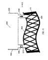
- FIG. 5 is a photograph of a micro-truss structure according to one embodiment of the present invention.
- FIG. 6 is a schematic cross-sectional diagram of a micro-truss structure according to one embodiment of the present invention.
- FIG. 7 is a schematic cross-sectional diagram of an apparatus for applying electroless deposition to a micro-truss structure according to one embodiment of the present invention.
- FIG. 8 is a schematic cross-sectional diagram of an apparatus for applying electrodeposition to a micro-truss structure according to one embodiment of the present invention.
- FIG. 9 is a schematic cross-sectional diagram of a micro-truss structure according to one embodiment of the present invention.
- FIG. 10 is a graph depicting data related to select embodiments of the present invention.
- FIG. 12 is a process flow diagram for forming a three-dimensional structure according to other embodiments of the present invention.
- a three-dimensional, curved (or “net-shape”), ordered micro-truss structure 10 is a self-supporting structure.
- the micro-truss structure 10 includes a plurality of angled struts (which may also be referred to as angled “truss elements,” “truss members,” or “polymer waveguides”) including first angled struts 12 , second angled struts 14 , and third angled struts 16 , which extend along a first direction A, a second direction B, and a third direction C, respectively.
- the micro-truss 10 may also include vertical struts 18 , which extend along a vertical direction D.
- the micro-truss further includes fourth angled struts 22 which extend along a fourth direction E and which also interpenetrate with the first, second, and third angled struts 12 , 14 , and 16 and the vertical struts 18 at nodes 20 .
- FIGS. 1 a , 1 b , 1 c , and 1 d depict a unit cell comprised of struts 12 , 14 , 16 , 18 , and 22 and node 20 .
- a plurality of ordered unit cells will comprise a micro-truss structure 10 .
- Unit cells are ordered when they are formed in repeating patterns within a micro-truss structure.
- These ordered unit cells are only some of many possible unit cell architectures that could be utilized for this application. Examples of additional possible ordered unit cell architectures include, but are not limited to, structures described in Jacobsen et al, Acta Materialia 56 (2008) 2540-254, the entire content of which is incorporated herein by reference.
- the struts 12 , 14 , 16 , and 18 may include a photo-polymer material.
- the struts 12 , 14 , 16 , and 18 may be polymer optical waveguides.
- the micro-truss 10 is formed by using a fixed light input (collimated UV light) to cure (polymerize) polymer optical waveguides, which can self-propagate in a 3D pattern. As such, the propagated polymer optical waveguides form the micro-truss structure 10 .
- some liquid polymers referred to as photopolymers, undergo a refractive index change during the polymerization process.
- the refractive index change can lead to a formation of polymer optical waveguides. If a monomer that is photo-sensitive is exposed to light (typically UV) under the right conditions, the initial area of polymerization, such as a small circular area, will “trap” the light and guide it to the tip of the polymerized region, further advancing that polymerized region. This process will continue, leading to the formation of a waveguide structure with substantially the same cross-sectional dimensions along its entire length.
- a mask with a two-dimensional pattern of apertures 340 (see FIGS. 4 a and 4 b ) is used with a light source and photo-monomer to create an ordered 3D polymer micro-truss structure (or an open-cell polymer micro-truss structure).
- FIG. 3 a is a schematic cross-sectional diagram of a system for forming a structure from multiple waveguides (or struts) created using a single collimated beam or multiple collimated beams passing through multiple apertures located at the bottom of the channel.
- a system for forming an ordered 3D polymer micro-truss structure includes one or more collimated light sources 300 , a channel/mold 310 having (or containing) photo-monomer 320 that will polymerize at a wavelength of collimated light beams provided by the light sources 300 , and a patterning apparatus, such as a mask 330 with one or more apertures (open areas) 340 .
- Each of the apertures 340 has a given shape and dimension substantially matching a cross-sectional geometry of a strut (e.g. waveguide 360 a ).
- the mask 330 rests on the transparent substrate (or transparent plate) 350 that includes the bottom of the channel/mold 310 .
- the mask 330 is made of a lightweight, flexible, and opaque material such as polyethylene terephthalate (PET) film.
- PET polyethylene terephthalate
- the transparent substrate 350 may be made of a material (such as quartz) that is transparent to the light emitted from the collimated light sources.
- the transparent substrate 350 acts as the mask 330 (e.g., portions of the transparent substrate 350 are opaque while other portions are transparent).
- the photo-monomer 320 fills the channel 310 above the mask 330 .
- different thicknesses of micro-truss structures can be achieved by filling the channel (or mold) 310 with photo-monomer 320 to the desired height. Once the collimated light source is applied, the intersecting polymer waveguides 360 a will grow upward from the surface of the mask 330 or the surface of the transparent substrate 350 , terminating at the free (e.g., upper) surface of the photo-monomer 320 in the channel 310 to form struts of the micro-truss structure.
- a 3D network (or micro-truss structure 360 ) can be formed because the intersecting polymer waveguides 360 a (or struts) will polymerize together, but will not interfere with waveguide propagation. Also, the spacing between the plurality of waveguides 360 a (or struts) corresponds with the pattern of the plurality of apertures 340 .
- the pattern of the apertures 340 may, for example, be in a square pattern as shown in FIG. 4 a and/or in a hexagonal pattern as shown in FIG. 4 b .
- the hole (aperture) spacing i.e., distance between apertures 340 in the mask 330 , and the number of waveguides 360 (or struts) formed from each of the apertures 340 will determine the open volume fraction (i.e. open space) of the formed ordered 3D micro-truss structure (or the formed open-cell polymer micro-truss structure).
- a three-dimensional, net-shape, ordered micro-truss structure 360 can be designed for various applications.
- the design parameters include: 1) the angle and pattern of the polymer struts with respect to one another, 2) the packing, or relative density of the resulting cell structure (or the open volume fraction), and 3) the cross-sectional shape and dimensions of the struts.
- the strut (or waveguide) diameter can range from 10 microns to 10 mm depending on the design criteria.
- the inclination at which the first, second, and third struts extend may be determined by an angle ⁇ (see, e.g., FIG. 3 a ) at which the collimated light sources 300 are oriented with respect to the mask 330 such that the collimated light passes through the apertures 340 of the mask 330 at an angle ⁇ . Due to the refractive index change between air and the mask and monomer, in many instances the angles of inclinations at the first, second, and third struts will not be the same as ⁇ .
- the struts further include vertical struts 360 b extending in a fourth direction with an inclination of substantially 90° (e.g., substantially perpendicular to the xz-plane).
- collimated light source 300 a is oriented to emit light in a direction substantially perpendicular with respect to the mask 330 .
- a single mask having a plurality of apertures which may have different sizes may be used, and collimated light aimed perpendicular to the plane of the mask or at an angle is selectively emitted through the apertures of the mask.
- At least one digital mask may be used in place of the mask 330 below, above, or to either side of the channel 370 , or in any combination of these locations between the collimated light sources and the photo-monomer 320 .
- a digital mask is a display device which can be controlled to become opaque at some locations and transparent at other locations to the wavelength of light used to polymerize the photo-monomer, such as a liquid crystal display (LCD).
- LCD liquid crystal display
- the digital mask is located between the collimated light sources 300 and the transparent substrate 350 .
- the digital mask can be configured on-the-fly to display any variation of aperture sizes and patterns to produce the desired micro-truss structure 360 , eliminating the need for stopping fabrication to change masks.
- the digital mask may be used to form differently sized apertures for the angled struts and the vertical struts.
- micro-truss structures have uses in a variety of fields, including advanced minor, heat exchange, light weight/high impact applications, etc. In many of these applications, it may be beneficial for the micro-truss structure to have a particular curvature that conforms to a surface where it will be used. For example in one embodiment, it may be beneficial for a micro-truss structure being used as armor to have a particular curvature that conforms to the outer surface of a military vehicle, or in another example, it may be beneficial for a micro-truss structure being used as a heat exchanger to comprise a particular curvature that conforms to the outside of an engine.
- the polymer micro-truss structure is first heated above its glass transition temperature (T g ).
- T g glass transition temperature
- the glass transition temperatures of various polymers are widely available and would be known to one having ordinary skill in the art.
- the micro-truss structure is elastically deformed into a desired curvature or shape.
- the deformed micro-truss structure is thermally post-cured such that the polymer is no longer elastically deformable.
- post-curing a micro-truss structure formed into a particular curvature may take approximately twenty-four hours at a temperature above 100° C.
- FIG. 5 is a photograph of a micro-truss structure that has been formed into a saddle shape and then thermally post-cured.
- the micro-truss structure 10 depicted in FIG. 6 includes two facesheets 402 , which have been attached to opposing sides of the micro-truss structure 10 .
- the facesheets 402 may be attached either before or after the micro-truss structure 10 is formed into a particular curvature.
- the attachment of the facesheets 402 to the micro-truss structure 10 creates a sandwich structure, which may have additional strength, stiffness, and thermal conductivity properties. Sandwich structures are well suited for applications that require high flexural stiffness at a minimal weight.
- either a single facesheet 402 or no facesheet 402 may be attached to the micro-truss structure 10 .
- FIG. 5 depicts a curved micro-truss structure without facesheets.
- the micro-truss structure 10 (i.e., the curved (or “net-shape”), ordered micro-truss structure) which has been formed into a particular curvature, is coated with another material to form a structure.
- the radius of the curvature may be as small as the thickness of the micro-truss structure 10 .
- a micro-truss structure 10 that is 2 cm thick may have a radius of curvature as small as 2 cm.
- FIG. 7 shows a schematic cross-sectional diagram of a micro-truss structure 10 being electroless plated according to one embodiment.
- This embodiment includes a heater 504 disposed within an electroless plating solution 516 contained within a reservoir 520 .
- the solution 516 is in communication with the micro-truss structure 10 through a first channel 506 and a second channel 510 .
- the second channel 510 includes a pump 508 , which functions to cycle the electroless plating solution 516 from the reservoir 520 into the micro-truss structure 10 .
- a catalyst for seeding electroless deposition onto the polymer micro-truss structure may be flowed through the micro-truss structure 10 using the same channels 506 , 510 and pump 508 as depicted in FIG. 7 .
- a metal coating 502 may be deposited upon the surface of the micro-truss structure 10 .
- the electroless plating process may initially coat the polymer truss with a metallic film and, if continued for a long period of time, may completely fill the void space with metal. In this way, the thickness of the metal coating can be controlled by adjusting the duration of the electroless plating process to be longer for thicker coatings or shorter for thinner coatings.
- FIG. 7 also includes a magnified view of a portion of the micro-truss structure 10 that is defined by a dotted square.
- the magnified portion depicts a connection point 512 between the micro-truss structure 10 and a faceplate 402 .
- the faceplate 402 may be comprised of a metal.
- the connection point 512 may include a polymer adhesive such as epoxy.
- a metal coating may be formed on the polymer adhesive during electroless plating. In some embodiments, this may be used to form a metallic bond between the faceplate 402 and the micro-truss structure 10 .
- a metallic bond between the faceplate 402 and the micro-truss structure 10 may increase the thermal exchange between the faceplate 402 and the micro-truss structure 10 allowing for a more efficient heat exchange device.
- FIG. 8 shows a schematic cross-sectional diagram of an embodiment of a micro-truss structure 10 being electroplated.
- the micro-truss structure 10 may first be electroless plated, as described above, to generate a sufficient conductive seed layer for electrodeposition to be applied.
- the apparatus for electrodeposition 612 depicted in FIG. 8 includes a pump 508 , a first channel 506 , a second channel 510 , and a reservoir 520 containing an electroplating solution 606 . Similar to the electroless plating apparatus depicted in FIG. 7 , the pump 508 in FIG.
- the apparatus for electrodeposition 612 includes a counter electrode 602 , a working electrode 604 , and an insulating facesheet 608 .
- the working electrode 604 has an electrical connection with the electroless plated micro-truss structure 10 causing the entire micro-truss structure 10 to function as a working electrode 604 .
- the electric field generated by the working electrode 604 and the counter electrode 602 may cause metal to deposit on the surface of the micro-truss structure 10 .
- each of the hollow metal struts may have an inner diameter in the range of 10 microns to 10 mm and the thickness of the metal (or the wall thickness) may be in the range of 1 micron to 1 mm.
- the resulting metal micro-truss structure may have a relative density in the range 0.5% to 30% with respect to a solid metal block.
- FIG. 9 shows a heat exchange device 802 including a metal-coated polymer micro-truss structure core 10 according to one embodiment of the present invention.
- the metal coating may have been applied to the micro-truss structure 10 through electroless deposition, electrodeposition, or some other coating method known in the art.
- the micro-truss structure 10 in this embodiment includes two facesheets 402 attached to the micro-truss structure 10 .
- the facesheets 402 may be comprised of a metal and have a metallic connection with the micro-truss structure 10 , which may increase the thermal conductivity of the overall heat exchange device 802 .
- the micro-truss structure 10 has been formed to have a particular curvature, which may allow the heat exchange device 802 to conform to a particular surface where it will be used.
- the micro-truss structure 10 may be formed to have a cylindrical shape to conform to the outside of a pipe.
- the micro-truss structure 10 may be formed to have a saddle shape to conform to a similarly shaped apparatus.
- the micro-truss structure 10 may be formed into any number of shapes to better conform to the surface where it will be applied.
- the heat exchange device 802 may contain a working fluid 804 , which is pumped from an attached apparatus (not shown) into the micro-truss structure 10 where it is cooled before being pumped back into the attached apparatus.
- the heat exchange device 802 may contain a working fluid 804 , which is pumped into the micro-truss structure 10 where it is heated before being pumped back into the attached apparatus (not shown).
- FIG. 10 shows a graph which compares the thermal resistance of two metal-coated polymer micro-truss structure based cold plates 704 , 706 to a polymer micro-truss structure based cold plate without a metal coating 702 .
- the micro-truss structure analyzed in the graph has a core thickness of 25 mm, a polymer truss diameter of 170 microns, and uses water as a working fluid.
- micro-truss structure with 13 microns of copper 704 or 35 microns of copper 706 would increase their average thermal conductivity from ⁇ 0.4 W/(m*K) to 100 and 200 W/(m*K) respectively, resulting in a decrease in thermal resistance by approximately an order of magnitude at constant pumping power per cooling area.
- the increase in thermal conductivity would greatly enhance the ability of the micro-truss structure to function as a heat exchange device.
- a micro-truss structure having a particular curvature could be used in a variety of different fields. Many of these uses may require that the micro-truss structure include particular materials.
- the micro-truss structure may be formed into a particular curvature and then left without a coating.
- the polymer from the micro-truss structure may be removed and replaced with another material. Examples of materials that may function as either a micro-truss structure material or as coatings include polymers, carbons/graphite, metals, and ceramics.
- micro-truss structure materials may be applied as a coating or incorporated into the micro-truss structure material after the structure has been formed to a particular curvature and cured to maintain that curvature.
- Methods of applying the coating to the structure or incorporating the material into the micro-truss structure include but are not limited to electrodeposition, electroless deposition, metal salt reduction, metal casting, gel casting, slip casting, sol-gel, chemical vapor deposition, carbide reactions, and preceramic polymers. Each of these methods is disclosed in Jacobsen et al., “Composite Structures With Ordered Three-Dimensional (3D) Continuous Interpenetrating Phases,” U.S. application Ser. No. 12/008,479, filed Jan. 11, 2008, now U.S. Pat. No. 8,320,727, which is incorporated by reference herein in its entirety.
- FIG. 11 shows a method of forming a three-dimensional, net-shape, ordered micro-truss structure according to an embodiment of the present invention.
- a volume photo-monomer is provided in block 902 .
- a mask is provided between at least one collimated light source and the volume of the photo-monomer, the mask having a plurality of apertures.
- a collimated light beam is directed onto the mask in block 906 such that a portion of the collimated light beam passes through the mask and is guided by the plurality of apertures into the photo-monomer to form a plurality of polymer waveguides.
- the uncured monomer is removed leaving behind the micro-truss structure (i.e., the partially cured, three-dimensional, ordered micro-truss structure).
- the micro-truss structure is heated above its glass transition temperature. Once above its glass transition temperature, the micro-truss structure may be elastically deformed into a curved structure as recited in block 912 . After the micro-truss structure is deformed into a desired curvature or shape, the micro-truss structure is thermally post-cured in block 914 (to thus form the curved (or (net-shape”), three-dimensional, ordered micro-truss structure). In some embodiments, an additional step of attaching a faceplate to a side of the micro-truss structure may be performed prior to block 910 , prior to block 912 , prior to block 914 , or after block 914 .
- FIG. 12 depicts additional embodiments of the method described in FIG. 11 .
- a coating may be applied to the micro-truss structure.
- the coating may be a metallic coating, and it may be applied through electroless deposition or electrodeposition.
- the polymer waveguide may be removed through etching, burning, or some other method known in the art.
- the micro-truss structure may comprise hollow tubes. As depicted in FIG. 12 the dotted line connecting block 1002 to block 1004 designates that in some embodiments the process described in block 1002 may be applied without applying the process described in block 1004 .
Abstract
Description
Claims (12)
Priority Applications (5)
| Application Number | Priority Date | Filing Date | Title |
|---|---|---|---|
| US13/312,952 US9539773B2 (en) | 2011-12-06 | 2011-12-06 | Net-shape structure with micro-truss core |
| CN201280060393.4A CN104114478B (en) | 2011-12-06 | 2012-03-23 | There is the reticulated structure of miniature truss core |
| EP12856497.8A EP2788278B1 (en) | 2011-12-06 | 2012-03-23 | Method of manufactoring a net-shape structure with micro-truss core |
| PCT/US2012/030414 WO2013085561A1 (en) | 2011-12-06 | 2012-03-23 | Net-shape structure with micro-truss core |
| US15/348,812 US10288359B2 (en) | 2011-12-06 | 2016-11-10 | Net-shape structure with micro-truss core |
Applications Claiming Priority (1)
| Application Number | Priority Date | Filing Date | Title |
|---|---|---|---|
| US13/312,952 US9539773B2 (en) | 2011-12-06 | 2011-12-06 | Net-shape structure with micro-truss core |
Related Child Applications (1)
| Application Number | Title | Priority Date | Filing Date |
|---|---|---|---|
| US15/348,812 Division US10288359B2 (en) | 2011-12-06 | 2016-11-10 | Net-shape structure with micro-truss core |
Publications (2)
| Publication Number | Publication Date |
|---|---|
| US20130143060A1 US20130143060A1 (en) | 2013-06-06 |
| US9539773B2 true US9539773B2 (en) | 2017-01-10 |
Family
ID=48524231
Family Applications (2)
| Application Number | Title | Priority Date | Filing Date |
|---|---|---|---|
| US13/312,952 Active 2032-12-30 US9539773B2 (en) | 2011-12-06 | 2011-12-06 | Net-shape structure with micro-truss core |
| US15/348,812 Active 2032-07-08 US10288359B2 (en) | 2011-12-06 | 2016-11-10 | Net-shape structure with micro-truss core |
Family Applications After (1)
| Application Number | Title | Priority Date | Filing Date |
|---|---|---|---|
| US15/348,812 Active 2032-07-08 US10288359B2 (en) | 2011-12-06 | 2016-11-10 | Net-shape structure with micro-truss core |
Country Status (4)
| Country | Link |
|---|---|
| US (2) | US9539773B2 (en) |
| EP (1) | EP2788278B1 (en) |
| CN (1) | CN104114478B (en) |
| WO (1) | WO2013085561A1 (en) |
Cited By (1)
| Publication number | Priority date | Publication date | Assignee | Title |
|---|---|---|---|---|
| US20180058770A1 (en) * | 2016-09-01 | 2018-03-01 | Additive Rocket Corporation | Structural heat exchanger |
Families Citing this family (64)
| Publication number | Priority date | Publication date | Assignee | Title |
|---|---|---|---|---|
| US9375864B2 (en) | 2007-05-10 | 2016-06-28 | Hrl Laboratories, Llc | Architected materials for enhanced energy absorption |
| US9017806B2 (en) * | 2012-03-23 | 2015-04-28 | Hrl Laboratories, Llc | High airflow micro-truss structural apparatus |
| US20150047463A1 (en) | 2012-06-26 | 2015-02-19 | California Institute Of Technology | Systems and methods for implementing bulk metallic glass-based macroscale gears |
| US9527261B1 (en) * | 2012-09-14 | 2016-12-27 | Hrl Laboratories, Llc | Hollow polymer micro-truss structures containing pressurized fluids |
| US20140342179A1 (en) | 2013-04-12 | 2014-11-20 | California Institute Of Technology | Systems and methods for shaping sheet materials that include metallic glass-based materials |
| WO2015006421A1 (en) | 2013-07-09 | 2015-01-15 | United Technologies Corporation | Metal-encapsulated polymeric article |
| WO2015006433A2 (en) | 2013-07-09 | 2015-01-15 | United Technologies Corporation | Plated polymer fan |
| US11267576B2 (en) | 2013-07-09 | 2022-03-08 | Raytheon Technologies Corporation | Plated polymer nosecone |
| EP3019723A4 (en) | 2013-07-09 | 2017-05-10 | United Technologies Corporation | Plated polymer compressor |
| WO2015073098A2 (en) * | 2013-08-27 | 2015-05-21 | University Of Virginia Patent Foundation | Three-dimensional space frames assembled from component pieces and methods for making the same |
| US10061078B1 (en) * | 2013-12-26 | 2018-08-28 | Hrl Laboratories, Llc | Polymer microlattice structures with multifunctional coatings for substrate bonding |
| US9884436B2 (en) * | 2014-04-17 | 2018-02-06 | GM Global Technology Operations LLC | Method for making a curved sandwich structure using a reconfigurable UV source mounting element |
| US9751287B2 (en) * | 2014-04-17 | 2017-09-05 | GM Global Technology Operations LLC | Low energy process for making curved sandwich structures with little or no residual stress |
| US10105941B2 (en) * | 2014-04-25 | 2018-10-23 | GM Global Technology Operations LLC | Stiffening and/or strengthening a structural member using a pre-made microtruss insert |
| US9925440B2 (en) | 2014-05-13 | 2018-03-27 | Bauer Hockey, Llc | Sporting goods including microlattice structures |
| US9511540B2 (en) * | 2014-08-07 | 2016-12-06 | GM Global Technology Operations LLC | Process for securing a micro-truss structure to a panel |
| US9733429B2 (en) * | 2014-08-18 | 2017-08-15 | Hrl Laboratories, Llc | Stacked microlattice materials and fabrication processes |
| US9783324B2 (en) * | 2014-08-26 | 2017-10-10 | The Boeing Company | Vessel insulation assembly |
| US10222144B2 (en) | 2014-09-23 | 2019-03-05 | The Boeing Company | Methods and apparatus for a microtruss heat exchanger |
| US9920429B2 (en) * | 2014-12-01 | 2018-03-20 | Raytheon Company | Method for manufacturing polymer-metal composite structural component |
| JP6856976B2 (en) * | 2014-12-15 | 2021-04-14 | ザ・ボーイング・カンパニーThe Boeing Company | Container insulation assembly |
| US10895015B1 (en) | 2014-12-16 | 2021-01-19 | Hrl Laboratories, Llc | Thin-walled high temperature alloy structures via multi-material additive manufacturing |
| WO2016100410A1 (en) * | 2014-12-16 | 2016-06-23 | Hrl Laboratories, Llc | Curved high temperature alloy sandwich panel with a truss core and fabrication method |
| US10408997B1 (en) | 2014-12-16 | 2019-09-10 | Hrl Laboratories, Llc | Net shape ceramic microtruss and ceramic microtruss with metal shell |
| US10487934B2 (en) | 2014-12-17 | 2019-11-26 | California Institute Of Technology | Systems and methods for implementing robust gearbox housings |
| US10358821B2 (en) * | 2015-03-02 | 2019-07-23 | The Boeing Company | Thermoplastic truss structure for use in wing and rotor blade structures and methods for manufacture |
| US10151377B2 (en) | 2015-03-05 | 2018-12-11 | California Institute Of Technology | Systems and methods for implementing tailored metallic glass-based strain wave gears and strain wave gear components |
| US10174780B2 (en) | 2015-03-11 | 2019-01-08 | California Institute Of Technology | Systems and methods for structurally interrelating components using inserts made from metallic glass-based materials |
| US10155412B2 (en) | 2015-03-12 | 2018-12-18 | California Institute Of Technology | Systems and methods for implementing flexible members including integrated tools made from metallic glass-based materials |
| US10502501B1 (en) * | 2015-04-01 | 2019-12-10 | Hrl Laboratories, Llc | Louvered elliptical tube micro-lattice heat exchangers |
| CN106042607A (en) * | 2015-04-17 | 2016-10-26 | 通用汽车环球科技运作有限责任公司 | Method for preparing bent sandwich structure by using reconfigurable UV-source installation element |
| US10399909B1 (en) | 2015-06-23 | 2019-09-03 | Hrl Laboratories, Llc | Ordered cellular structures and methods of manufacturing the same |
| US20180015684A1 (en) * | 2015-06-26 | 2018-01-18 | Steven D. Lieberman | Cell structure for composite sandwich core and method of making sandwich panels |
| US10232583B2 (en) | 2015-08-25 | 2019-03-19 | Hrl Laboratories, Llc | Sparse truss structures and methods of making the same |
| EP3341322B1 (en) * | 2015-08-25 | 2020-10-07 | HRL Laboratories LLC | Sparse truss structures and methods of making the same |
| US10968527B2 (en) * | 2015-11-12 | 2021-04-06 | California Institute Of Technology | Method for embedding inserts, fasteners and features into metal core truss panels |
| FR3047727B1 (en) * | 2016-02-17 | 2019-06-07 | Thales | MONOBLOC STRUCTURE FOR SATELLITE PANEL |
| US11135829B2 (en) * | 2016-09-30 | 2021-10-05 | The Boeing Company | System and method for making pin reinforced sandwich panel and resulting panel structure |
| US10061201B2 (en) * | 2016-10-24 | 2018-08-28 | Hrl Laboratories, Llc | Bottom up apparatus design for formation of self-propagating photopolymer waveguides |
| US11085708B2 (en) * | 2016-10-28 | 2021-08-10 | International Business Machines Corporation | Method for improved thermal performance of cold plates and heat sinks |
| US10179428B2 (en) | 2016-11-17 | 2019-01-15 | The Boeing Company | Mechanically reinforced foam insulation panel and methods of making the same |
| JP2020512482A (en) | 2017-03-10 | 2020-04-23 | カリフォルニア インスティチュート オブ テクノロジー | Manufacturing method of wave gear flexspline using metal additive manufacturing |
| US10384394B2 (en) * | 2017-03-15 | 2019-08-20 | Carbon, Inc. | Constant force compression lattice |
| EP3630395A4 (en) | 2017-05-24 | 2020-11-25 | California Institute of Technology | Hypoeutectic amorphous metal-based materials for additive manufacturing |
| WO2018223117A2 (en) | 2017-06-02 | 2018-12-06 | California Institute Of Technology | High toughness metallic glass-based composites for additive manufacturing |
| US11358350B1 (en) * | 2017-06-30 | 2022-06-14 | Hrl Laboratories, Llc | Lightweight sandwich structures and methods of manufacturing the same |
| US10744711B2 (en) * | 2017-07-10 | 2020-08-18 | Carbon, Inc. | Surface feature arrays for additively manufactured products |
| CN107473177B (en) * | 2017-07-14 | 2020-07-14 | 华中科技大学 | Manufacturing method of 3D (three-dimensional) micro-nano structure |
| JP2020528536A (en) * | 2017-07-27 | 2020-09-24 | オックスフォード ナノシステムズ リミテッド | Heat exchange element with microstructure coating and manufacturing method |
| TWI638129B (en) * | 2017-11-29 | 2018-10-11 | 財團法人工業技術研究院 | Flow channel structure for heat exchanger |
| US11393773B1 (en) | 2017-12-08 | 2022-07-19 | Hrl Laboratories, Llc | Stress isolating interposer and sensor package and method of manufacturing the same |
| US11426938B2 (en) | 2018-02-21 | 2022-08-30 | Carbon, Inc. | Rapid wash system for additive manufacturing |
| US11230050B2 (en) | 2018-02-27 | 2022-01-25 | Carbon, Inc. | Lattice base structures for additive manufacturing |
| US11541600B2 (en) | 2018-03-20 | 2023-01-03 | Carbon, Inc. | Rapid wash carrier platform for additive manufacturing of dental models |
| US11104096B2 (en) * | 2018-08-30 | 2021-08-31 | The Boeing Company | Integrated fastener insert for open cellular sandwich structure and method to install |
| CN109440089B (en) * | 2018-10-26 | 2021-02-02 | 东南大学 | Metal foil type strain gauge design and manufacturing method based on hybrid 3D printing technology |
| US11680629B2 (en) | 2019-02-28 | 2023-06-20 | California Institute Of Technology | Low cost wave generators for metal strain wave gears and methods of manufacture thereof |
| US11859705B2 (en) | 2019-02-28 | 2024-01-02 | California Institute Of Technology | Rounded strain wave gear flexspline utilizing bulk metallic glass-based materials and methods of manufacture thereof |
| US11400613B2 (en) | 2019-03-01 | 2022-08-02 | California Institute Of Technology | Self-hammering cutting tool |
| US11591906B2 (en) | 2019-03-07 | 2023-02-28 | California Institute Of Technology | Cutting tool with porous regions |
| WO2020232550A1 (en) | 2019-05-21 | 2020-11-26 | Bauer Hockey Ltd. | Helmets comprising additively-manufactured components |
| US11130131B2 (en) * | 2019-09-26 | 2021-09-28 | Lawrence Livermore National Security, Llc | Lattice microfluidics |
| US11688596B2 (en) | 2021-02-12 | 2023-06-27 | Lawrence Livermore National Security, Llc | Systems and methods lattice spray substrates for mass spectrometry |
| CN113720193B (en) * | 2021-08-12 | 2022-06-07 | 西安交通大学 | Material increase manufacturing-oriented alveolus bionic super heat exchanger structure and preparation method thereof |
Citations (80)
| Publication number | Priority date | Publication date | Assignee | Title |
|---|---|---|---|---|
| US4219597A (en) | 1978-05-05 | 1980-08-26 | Societe Europeene De Propulsion | Three-dimensional, multi-directional structure |
| JPS56169764A (en) * | 1980-05-28 | 1981-12-26 | Hitachi Chem Co Ltd | Device for electroless copper plating |
| US4399020A (en) * | 1981-07-24 | 1983-08-16 | Diamond Shamrock Corporation | Device for waste water treatment |
| US4400421A (en) | 1982-12-09 | 1983-08-23 | The United States Of America As Represented By The Secretary Of The Air Force | Four-directional structure for reinforcement |
| US4568595A (en) | 1984-04-26 | 1986-02-04 | Morris Jeffrey R | Coated ceramic structure and method of making same |
| US4575330A (en) | 1984-08-08 | 1986-03-11 | Uvp, Inc. | Apparatus for production of three-dimensional objects by stereolithography |
| US4722089A (en) | 1985-12-16 | 1988-01-26 | Lytel, Incorporated | Phase locked diode laser array |
| US4815386A (en) * | 1984-07-17 | 1989-03-28 | Alloy Surfaces Company, Inc. | Pyrophoric material with metal skeleton |
| US5006937A (en) | 1985-12-06 | 1991-04-09 | Canon Kabushiki Kaisha | Imaging data processing apparatus |
| US5185297A (en) | 1986-09-16 | 1993-02-09 | Lanxide Technology Company, Lp | Ceramic foams |
| US5265185A (en) | 1992-10-02 | 1993-11-23 | The United States Of America As Represented By The Secretary Of The Army | Optical waveguides in electro-optical polymers and method |
| US5394490A (en) | 1992-08-11 | 1995-02-28 | Hitachi, Ltd. | Semiconductor device having an optical waveguide interposed in the space between electrode members |
| US5401694A (en) | 1987-01-13 | 1995-03-28 | Lanxide Technology Company, Lp | Production of metal carbide articles |
| US5402514A (en) | 1988-01-15 | 1995-03-28 | E. I. Du Pont De Nemours And Company | Optical waveguide devices including dry photohardenable layers |
| US5932397A (en) | 1996-05-28 | 1999-08-03 | Rvm Scientific, Inc. | Multicolor lithography for control of three dimensional refractive index gradient processing |
| US5938845A (en) * | 1995-10-20 | 1999-08-17 | Aiwa Co., Ltd. | Uniform heat distribution apparatus and method for electroless nickel plating in fabrication of thin film head gaps |
| US5954898A (en) * | 1994-05-13 | 1999-09-21 | Lockheed Fort Worth Company | Method and system for fabricating parts from composite materials |
| US6176874B1 (en) | 1993-10-18 | 2001-01-23 | Masschusetts Institute Of Technology | Vascularized tissue regeneration matrices formed by solid free form fabrication techniques |
| US6274288B1 (en) | 1995-06-12 | 2001-08-14 | California Institute Of Technology | Self-trapping and self-focusing of optical beams in photopolymers |
| JP2001312044A (en) | 2000-05-01 | 2001-11-09 | Ricoh Opt Ind Co Ltd | Density distribution mask and method for manufacturing three-dimensional structure using the same |
| US6341190B1 (en) | 1993-10-01 | 2002-01-22 | Epigem Limited | Organic optical components and preparation thereof |
| US6379962B1 (en) | 1997-11-14 | 2002-04-30 | Bonetec Corporation | Polymer scaffold having microporous polymer struts defining interconnected macropores |
| US6472210B1 (en) | 1997-11-14 | 2002-10-29 | Bonetec Corporation | Polymer scaffold having microporous polymer struts defining interconnected macropores |
| US6500401B2 (en) | 2000-07-20 | 2002-12-31 | Cabot Corporation | Carbon foams and methods of making the same |
| US6510260B2 (en) | 2001-01-02 | 2003-01-21 | Finisar Corporation, Inc. | N×N optical switching device based on thermal optic induced internal reflection effect |
| US6592787B2 (en) | 1997-03-31 | 2003-07-15 | Porvair Corporation | Porous articles and method for the manufacture thereof |
| US6631231B2 (en) | 2000-03-21 | 2003-10-07 | Matsushita Electric Industrial Co., Ltd. | Optical waveguide elements, optical wavelength conversion elements, and process for producing optical waveguide elements |
| US6650817B2 (en) | 2000-12-29 | 2003-11-18 | Intel Corporation | Multi-level waveguide |
| US6660192B1 (en) | 1996-03-15 | 2003-12-09 | Harvard College | Molded waveguides |
| US6670039B1 (en) | 1996-07-11 | 2003-12-30 | Dennis C. Nagle | Carbonized wood and materials formed therefrom |
| CN1464934A (en) | 2000-07-28 | 2003-12-31 | 布莱阿姆青年大学 | Iso-truss structure |
| US6684007B2 (en) | 1998-10-09 | 2004-01-27 | Fujitsu Limited | Optical coupling structures and the fabrication processes |
| US20040021237A1 (en) | 2002-08-01 | 2004-02-05 | Fuji Xerox Co., Ltd. | Process for producing polymer optical waveguide |
| US20040145967A1 (en) | 2001-05-28 | 2004-07-29 | Yamatake Corporation | Micro-mixer |
| US20040154252A1 (en) | 2002-06-06 | 2004-08-12 | Sypeck David J. | Multifunctional periodic cellular solids and the method of making same |
| US20040200417A1 (en) | 2002-06-05 | 2004-10-14 | Applied Materials, Inc. | Very low temperature CVD process with independently variable conformality, stress and composition of the CVD layer |
| US6823116B2 (en) | 2001-08-13 | 2004-11-23 | Toyoda Gosei Co., Ltd. | Optical waveguide device manufacturing jig, method of manufacturing optical waveguide device by use of the same jig, and the same optical waveguide device |
| US20040253365A1 (en) | 2001-08-23 | 2004-12-16 | Warren William L. | Architecture tool and methods of use |
| US20040264863A1 (en) | 2001-02-08 | 2004-12-30 | Kouichi Suzuki | Optical coupler |
| WO2005014216A2 (en) | 2003-02-14 | 2005-02-17 | University Of Virginia Patent Foundation | Methods for manufacture of multilayered multifunctional truss structures and related structures there from |
| US6862393B2 (en) | 2000-03-15 | 2005-03-01 | Nozomi Photonics Co., Ltd. | Optical waveguide element, manufacturing method for optical waveguide element, optical deflecting element, and optical switching element |
| US6870976B2 (en) | 2001-03-13 | 2005-03-22 | Opnext, Inc. | Filter based multiplexer/demultiplexer component |
| US6879757B1 (en) | 2001-12-11 | 2005-04-12 | Phosistor Technologies, Inc. | Connection between a waveguide array and a fiber array |
| US6887809B1 (en) | 2000-09-04 | 2005-05-03 | Fraunhofer-Gesellschaft Zur Foerderung Der Angewandten Forschung E.V. | Open-celled silicon carbide foam ceramic and method for production thereof |
| US6898362B2 (en) | 2002-01-17 | 2005-05-24 | Micron Technology Inc. | Three-dimensional photonic crystal waveguide structure and method |
| US20050135745A1 (en) | 2003-03-10 | 2005-06-23 | Greiner Christoph M. | Optical structures distributed among multiple optical waveguides |
| US6932880B2 (en) | 2001-06-12 | 2005-08-23 | Toyoda Gosei Co., Ltd. | Method of manufacturing optical waveguide device |
| US6941888B2 (en) | 2003-12-16 | 2005-09-13 | Roshdy George S. Barsoum | Hybrid ship hull |
| US20050202206A1 (en) | 2002-05-30 | 2005-09-15 | Wadley Haydn N.G. | Method for manufacture of periodic cellular structure and resulting periodic cellular structure |
| US6952504B2 (en) | 2001-12-21 | 2005-10-04 | Neophotonics Corporation | Three dimensional engineering of planar optical structures |
| US20050221156A1 (en) * | 2004-04-06 | 2005-10-06 | Mclean Gerard F | Method for forming compact chemical reactors with reactor frames |
| US20050224449A1 (en) | 2002-03-05 | 2005-10-13 | Jerwei Hsieh | Corner compensation method for fabricating MEMS and structure thereof |
| US20050255289A1 (en) | 2002-07-25 | 2005-11-17 | Wadley Haydn N | Method for manufacture of cellular materials and structures for blast and impact mitigation and resulting structure |
| US20050287696A1 (en) | 2004-06-29 | 2005-12-29 | Patrick Dumais | Waveguiding structures with embedded microchannels and method for fabrication thereof |
| US6993235B2 (en) | 2004-02-23 | 2006-01-31 | Canon Kabushiki Kaisha | Three-dimensional periodic structure and functional element including the same |
| US6993406B1 (en) | 2003-04-24 | 2006-01-31 | Sandia Corporation | Method for making a bio-compatible scaffold |
| US20060029349A1 (en) | 2004-08-04 | 2006-02-09 | Canon Kabushiki Kaisha | Three-dimensional photonic crystal and optical element |
| US20060029348A1 (en) | 2002-02-19 | 2006-02-09 | Optinetrics, Inc. | Optical waveguide structure |
| US7006747B2 (en) | 2003-01-17 | 2006-02-28 | 3M Innovative Properties Company | Optical devices incorporating photo reactive polymers |
| US7014661B2 (en) | 2000-06-23 | 2006-03-21 | University College London | Transcutaneous prosthesis |
| US7020374B2 (en) | 2003-02-03 | 2006-03-28 | Freescale Semiconductor, Inc. | Optical waveguide structure and method for fabricating the same |
| US7022522B2 (en) | 1998-11-13 | 2006-04-04 | Limin Guan | Macroporous polymer scaffold containing calcium phosphate particles |
| US7024093B2 (en) | 2002-12-02 | 2006-04-04 | Shipley Company, Llc | Methods of forming waveguides and waveguides formed therefrom |
| US7085467B2 (en) | 2004-03-08 | 2006-08-01 | Canon Kabushiki Kaisha | Three-dimensional periodic structure, functional element including the same, and light-emitting device |
| US7209622B2 (en) | 2005-06-07 | 2007-04-24 | Canon Kabushiki Kaisha | Resonator and light emitting device using the same |
| US20070196066A1 (en) | 2006-02-21 | 2007-08-23 | Canon Kabushiki Kaisha | Process for formation of three-dimensional photonic crystal |
| US20070235170A1 (en) * | 2006-04-06 | 2007-10-11 | Brian Zinck | Method and apparatus for heat exchanging |
| US20070247714A1 (en) | 2004-08-05 | 2007-10-25 | Marc Schnieper | Security Device |
| US7382959B1 (en) | 2006-10-13 | 2008-06-03 | Hrl Laboratories, Llc | Optically oriented three-dimensional polymer microstructures |
| US7421159B2 (en) | 2005-12-13 | 2008-09-02 | Board of Supervisor of Louisiana State University and Agricultural and Mechanical College | Integral pre-aligned micro-optical systems |
| US7531120B2 (en) | 2000-12-02 | 2009-05-12 | Aquamarijn Holding B.V. | Method of making a product with a micro or nano sized structure and product |
| US7609922B2 (en) | 2006-03-27 | 2009-10-27 | Fujitsu Limited | Optical module, optical transmission system, and fabrication method for optical module |
| US7653276B1 (en) | 2008-03-06 | 2010-01-26 | Hrl Laboratories, Llc | Composite structures for storing thermal energy |
| US7687132B1 (en) | 2008-03-05 | 2010-03-30 | Hrl Laboratories, Llc | Ceramic microtruss |
| US20100124659A1 (en) * | 2008-11-19 | 2010-05-20 | The Boeing Company | Staged cocuring of composite structures |
| US20100159303A1 (en) * | 2008-12-22 | 2010-06-24 | Gm Global Technology Operations, Inc. | Fuel cell fabrication using photopolymer based processes |
| CN201580542U (en) | 2009-12-02 | 2010-09-15 | 中国海洋大学 | Single-pole platform of triangular truss |
| US20100300669A1 (en) * | 2009-06-01 | 2010-12-02 | Alan Jon Jacobsen | Methods and apparatus for a micro-truss based structural insulation layer |
| US7901462B2 (en) | 2005-06-23 | 2011-03-08 | Depuy Products, Inc. | Implants with textured surface and methods for producing the same |
| US8453717B1 (en) * | 2009-07-20 | 2013-06-04 | Hrl Laboratories, Llc | Micro-architected materials for heat sink applications |
Family Cites Families (1)
| Publication number | Priority date | Publication date | Assignee | Title |
|---|---|---|---|---|
| DE60138627D1 (en) * | 2000-07-14 | 2009-06-18 | Univ Virginia | FOAM FOR HEAT EXCHANGE |
-
2011
- 2011-12-06 US US13/312,952 patent/US9539773B2/en active Active
-
2012
- 2012-03-23 WO PCT/US2012/030414 patent/WO2013085561A1/en active Application Filing
- 2012-03-23 EP EP12856497.8A patent/EP2788278B1/en active Active
- 2012-03-23 CN CN201280060393.4A patent/CN104114478B/en active Active
-
2016
- 2016-11-10 US US15/348,812 patent/US10288359B2/en active Active
Patent Citations (91)
| Publication number | Priority date | Publication date | Assignee | Title |
|---|---|---|---|---|
| US4219597A (en) | 1978-05-05 | 1980-08-26 | Societe Europeene De Propulsion | Three-dimensional, multi-directional structure |
| JPS56169764A (en) * | 1980-05-28 | 1981-12-26 | Hitachi Chem Co Ltd | Device for electroless copper plating |
| US4399020A (en) * | 1981-07-24 | 1983-08-16 | Diamond Shamrock Corporation | Device for waste water treatment |
| US4400421A (en) | 1982-12-09 | 1983-08-23 | The United States Of America As Represented By The Secretary Of The Air Force | Four-directional structure for reinforcement |
| US4568595A (en) | 1984-04-26 | 1986-02-04 | Morris Jeffrey R | Coated ceramic structure and method of making same |
| US4815386A (en) * | 1984-07-17 | 1989-03-28 | Alloy Surfaces Company, Inc. | Pyrophoric material with metal skeleton |
| US4575330A (en) | 1984-08-08 | 1986-03-11 | Uvp, Inc. | Apparatus for production of three-dimensional objects by stereolithography |
| US4575330B1 (en) | 1984-08-08 | 1989-12-19 | ||
| US5006937A (en) | 1985-12-06 | 1991-04-09 | Canon Kabushiki Kaisha | Imaging data processing apparatus |
| US4722089A (en) | 1985-12-16 | 1988-01-26 | Lytel, Incorporated | Phase locked diode laser array |
| US5185297A (en) | 1986-09-16 | 1993-02-09 | Lanxide Technology Company, Lp | Ceramic foams |
| US5401694A (en) | 1987-01-13 | 1995-03-28 | Lanxide Technology Company, Lp | Production of metal carbide articles |
| US5402514A (en) | 1988-01-15 | 1995-03-28 | E. I. Du Pont De Nemours And Company | Optical waveguide devices including dry photohardenable layers |
| US5394490A (en) | 1992-08-11 | 1995-02-28 | Hitachi, Ltd. | Semiconductor device having an optical waveguide interposed in the space between electrode members |
| US5265185A (en) | 1992-10-02 | 1993-11-23 | The United States Of America As Represented By The Secretary Of The Army | Optical waveguides in electro-optical polymers and method |
| US6341190B1 (en) | 1993-10-01 | 2002-01-22 | Epigem Limited | Organic optical components and preparation thereof |
| US6176874B1 (en) | 1993-10-18 | 2001-01-23 | Masschusetts Institute Of Technology | Vascularized tissue regeneration matrices formed by solid free form fabrication techniques |
| US5954898A (en) * | 1994-05-13 | 1999-09-21 | Lockheed Fort Worth Company | Method and system for fabricating parts from composite materials |
| US6274288B1 (en) | 1995-06-12 | 2001-08-14 | California Institute Of Technology | Self-trapping and self-focusing of optical beams in photopolymers |
| US6387593B1 (en) | 1995-06-12 | 2002-05-14 | California Institute Of Technology | Self-trapping and self-focusing of optical beams in photopolymers |
| US5938845A (en) * | 1995-10-20 | 1999-08-17 | Aiwa Co., Ltd. | Uniform heat distribution apparatus and method for electroless nickel plating in fabrication of thin film head gaps |
| US6660192B1 (en) | 1996-03-15 | 2003-12-09 | Harvard College | Molded waveguides |
| US5932397A (en) | 1996-05-28 | 1999-08-03 | Rvm Scientific, Inc. | Multicolor lithography for control of three dimensional refractive index gradient processing |
| US6670039B1 (en) | 1996-07-11 | 2003-12-30 | Dennis C. Nagle | Carbonized wood and materials formed therefrom |
| US6592787B2 (en) | 1997-03-31 | 2003-07-15 | Porvair Corporation | Porous articles and method for the manufacture thereof |
| US6472210B1 (en) | 1997-11-14 | 2002-10-29 | Bonetec Corporation | Polymer scaffold having microporous polymer struts defining interconnected macropores |
| US6379962B1 (en) | 1997-11-14 | 2002-04-30 | Bonetec Corporation | Polymer scaffold having microporous polymer struts defining interconnected macropores |
| US6875442B2 (en) | 1997-11-14 | 2005-04-05 | Bonetec Corporation | Process for growing tissue in a biocompatible macroporous polymer scaffold and products therefrom |
| US6684007B2 (en) | 1998-10-09 | 2004-01-27 | Fujitsu Limited | Optical coupling structures and the fabrication processes |
| US7022522B2 (en) | 1998-11-13 | 2006-04-04 | Limin Guan | Macroporous polymer scaffold containing calcium phosphate particles |
| US6862393B2 (en) | 2000-03-15 | 2005-03-01 | Nozomi Photonics Co., Ltd. | Optical waveguide element, manufacturing method for optical waveguide element, optical deflecting element, and optical switching element |
| US6631231B2 (en) | 2000-03-21 | 2003-10-07 | Matsushita Electric Industrial Co., Ltd. | Optical waveguide elements, optical wavelength conversion elements, and process for producing optical waveguide elements |
| JP2001312044A (en) | 2000-05-01 | 2001-11-09 | Ricoh Opt Ind Co Ltd | Density distribution mask and method for manufacturing three-dimensional structure using the same |
| US7014661B2 (en) | 2000-06-23 | 2006-03-21 | University College London | Transcutaneous prosthesis |
| US6500401B2 (en) | 2000-07-20 | 2002-12-31 | Cabot Corporation | Carbon foams and methods of making the same |
| CN1464934A (en) | 2000-07-28 | 2003-12-31 | 布莱阿姆青年大学 | Iso-truss structure |
| US20050115186A1 (en) | 2000-07-28 | 2005-06-02 | Jensen David W. | Iso-truss structure |
| US6887809B1 (en) | 2000-09-04 | 2005-05-03 | Fraunhofer-Gesellschaft Zur Foerderung Der Angewandten Forschung E.V. | Open-celled silicon carbide foam ceramic and method for production thereof |
| US7531120B2 (en) | 2000-12-02 | 2009-05-12 | Aquamarijn Holding B.V. | Method of making a product with a micro or nano sized structure and product |
| US6650817B2 (en) | 2000-12-29 | 2003-11-18 | Intel Corporation | Multi-level waveguide |
| US6510260B2 (en) | 2001-01-02 | 2003-01-21 | Finisar Corporation, Inc. | N×N optical switching device based on thermal optic induced internal reflection effect |
| US20040264863A1 (en) | 2001-02-08 | 2004-12-30 | Kouichi Suzuki | Optical coupler |
| US6870976B2 (en) | 2001-03-13 | 2005-03-22 | Opnext, Inc. | Filter based multiplexer/demultiplexer component |
| US20040145967A1 (en) | 2001-05-28 | 2004-07-29 | Yamatake Corporation | Micro-mixer |
| US6932880B2 (en) | 2001-06-12 | 2005-08-23 | Toyoda Gosei Co., Ltd. | Method of manufacturing optical waveguide device |
| US6823116B2 (en) | 2001-08-13 | 2004-11-23 | Toyoda Gosei Co., Ltd. | Optical waveguide device manufacturing jig, method of manufacturing optical waveguide device by use of the same jig, and the same optical waveguide device |
| US6925233B2 (en) | 2001-08-13 | 2005-08-02 | Toyoda Gosei Co., Ltd. | Optical waveguide device manufacturing jig, method of manufacturing optical waveguide device by use of the same jig, and the same optical waveguide device |
| US20040253365A1 (en) | 2001-08-23 | 2004-12-16 | Warren William L. | Architecture tool and methods of use |
| US6879757B1 (en) | 2001-12-11 | 2005-04-12 | Phosistor Technologies, Inc. | Connection between a waveguide array and a fiber array |
| US6952504B2 (en) | 2001-12-21 | 2005-10-04 | Neophotonics Corporation | Three dimensional engineering of planar optical structures |
| US6898362B2 (en) | 2002-01-17 | 2005-05-24 | Micron Technology Inc. | Three-dimensional photonic crystal waveguide structure and method |
| US20060029348A1 (en) | 2002-02-19 | 2006-02-09 | Optinetrics, Inc. | Optical waveguide structure |
| US20050224449A1 (en) | 2002-03-05 | 2005-10-13 | Jerwei Hsieh | Corner compensation method for fabricating MEMS and structure thereof |
| US20050202206A1 (en) | 2002-05-30 | 2005-09-15 | Wadley Haydn N.G. | Method for manufacture of periodic cellular structure and resulting periodic cellular structure |
| US20040200417A1 (en) | 2002-06-05 | 2004-10-14 | Applied Materials, Inc. | Very low temperature CVD process with independently variable conformality, stress and composition of the CVD layer |
| US20040154252A1 (en) | 2002-06-06 | 2004-08-12 | Sypeck David J. | Multifunctional periodic cellular solids and the method of making same |
| US20050255289A1 (en) | 2002-07-25 | 2005-11-17 | Wadley Haydn N | Method for manufacture of cellular materials and structures for blast and impact mitigation and resulting structure |
| US20040021237A1 (en) | 2002-08-01 | 2004-02-05 | Fuji Xerox Co., Ltd. | Process for producing polymer optical waveguide |
| US7024093B2 (en) | 2002-12-02 | 2006-04-04 | Shipley Company, Llc | Methods of forming waveguides and waveguides formed therefrom |
| US7006747B2 (en) | 2003-01-17 | 2006-02-28 | 3M Innovative Properties Company | Optical devices incorporating photo reactive polymers |
| US7020374B2 (en) | 2003-02-03 | 2006-03-28 | Freescale Semiconductor, Inc. | Optical waveguide structure and method for fabricating the same |
| WO2005014216A2 (en) | 2003-02-14 | 2005-02-17 | University Of Virginia Patent Foundation | Methods for manufacture of multilayered multifunctional truss structures and related structures there from |
| US20060080835A1 (en) | 2003-02-14 | 2006-04-20 | Kooistra Gregory W | Methods for manufacture of multilayered multifunctional truss structures and related structures there from |
| US20050135745A1 (en) | 2003-03-10 | 2005-06-23 | Greiner Christoph M. | Optical structures distributed among multiple optical waveguides |
| US6993406B1 (en) | 2003-04-24 | 2006-01-31 | Sandia Corporation | Method for making a bio-compatible scaffold |
| US6941888B2 (en) | 2003-12-16 | 2005-09-13 | Roshdy George S. Barsoum | Hybrid ship hull |
| US6993235B2 (en) | 2004-02-23 | 2006-01-31 | Canon Kabushiki Kaisha | Three-dimensional periodic structure and functional element including the same |
| US7085467B2 (en) | 2004-03-08 | 2006-08-01 | Canon Kabushiki Kaisha | Three-dimensional periodic structure, functional element including the same, and light-emitting device |
| US20050221156A1 (en) * | 2004-04-06 | 2005-10-06 | Mclean Gerard F | Method for forming compact chemical reactors with reactor frames |
| US20050287696A1 (en) | 2004-06-29 | 2005-12-29 | Patrick Dumais | Waveguiding structures with embedded microchannels and method for fabrication thereof |
| US20060029349A1 (en) | 2004-08-04 | 2006-02-09 | Canon Kabushiki Kaisha | Three-dimensional photonic crystal and optical element |
| US20070247714A1 (en) | 2004-08-05 | 2007-10-25 | Marc Schnieper | Security Device |
| US7209622B2 (en) | 2005-06-07 | 2007-04-24 | Canon Kabushiki Kaisha | Resonator and light emitting device using the same |
| US7901462B2 (en) | 2005-06-23 | 2011-03-08 | Depuy Products, Inc. | Implants with textured surface and methods for producing the same |
| US7421159B2 (en) | 2005-12-13 | 2008-09-02 | Board of Supervisor of Louisiana State University and Agricultural and Mechanical College | Integral pre-aligned micro-optical systems |
| US20070196066A1 (en) | 2006-02-21 | 2007-08-23 | Canon Kabushiki Kaisha | Process for formation of three-dimensional photonic crystal |
| US7609922B2 (en) | 2006-03-27 | 2009-10-27 | Fujitsu Limited | Optical module, optical transmission system, and fabrication method for optical module |
| US20070235170A1 (en) * | 2006-04-06 | 2007-10-11 | Brian Zinck | Method and apparatus for heat exchanging |
| US7382959B1 (en) | 2006-10-13 | 2008-06-03 | Hrl Laboratories, Llc | Optically oriented three-dimensional polymer microstructures |
| US7653279B1 (en) | 2006-10-13 | 2010-01-26 | Hrl Laboratories, Llc | Optically oriented three-dimensional polymer microstructures |
| US7687132B1 (en) | 2008-03-05 | 2010-03-30 | Hrl Laboratories, Llc | Ceramic microtruss |
| US7653276B1 (en) | 2008-03-06 | 2010-01-26 | Hrl Laboratories, Llc | Composite structures for storing thermal energy |
| US7938989B1 (en) | 2008-03-06 | 2011-05-10 | Hrl Laboratories, Llc | Composite structures for storing thermal energy |
| US20100124659A1 (en) * | 2008-11-19 | 2010-05-20 | The Boeing Company | Staged cocuring of composite structures |
| US20100159303A1 (en) * | 2008-12-22 | 2010-06-24 | Gm Global Technology Operations, Inc. | Fuel cell fabrication using photopolymer based processes |
| CN101814614A (en) | 2008-12-22 | 2010-08-25 | 通用汽车环球科技运作公司 | Fuel cell fabrication using photopolymer based processes |
| US8268510B2 (en) | 2008-12-22 | 2012-09-18 | GM Global Technology Operations LLC | Fuel cell fabrication using photopolymer based processes |
| US20100300669A1 (en) * | 2009-06-01 | 2010-12-02 | Alan Jon Jacobsen | Methods and apparatus for a micro-truss based structural insulation layer |
| WO2010141176A2 (en) | 2009-06-01 | 2010-12-09 | The Boeing Company | Methods and apparatus for a micro-truss based structural insulation layer |
| US8453717B1 (en) * | 2009-07-20 | 2013-06-04 | Hrl Laboratories, Llc | Micro-architected materials for heat sink applications |
| CN201580542U (en) | 2009-12-02 | 2010-09-15 | 中国海洋大学 | Single-pole platform of triangular truss |
Non-Patent Citations (25)
| Title |
|---|
| Bertsch et al., "Microstereolithography: A Review", Materials Research Society Symposium Proceedings, 2003, 1-13, vol. 758, USA. |
| Chuang et al., "A New Method to Fabricate Polymer Waveguides", Progress in Electromagnetics Research Symposium, Aug. 22-26, 2005, 92-95, Hangzhou, China. |
| English translation of Chinese Office action for Chinese Patent Application No. 201280060393.4, mailed Jul. 3, 2015, 9 pages. |
| Evans, et al "Concepts for enhanced energy absorption using hollow micro-lattices", International Journal of Impact Engineering, 37 (2010) pp. 947-959. * |
| Extended European Search Report for Application No. 12856497.8, dated Jul. 6, 2015, 9 pages. |
| International Search Report and Written Opinion for PCT/US2012/030414 dated Jul. 9, 2012, 6 pages. |
| Jacobsen et al., "Micro-scale truss structures with three-filed and six-fold symmetry formed from self-propagating polymer waveguides," Acta Materialia, 56:2540-2548, 2008. |
| Jacobsen, et al "Interconnected Self-Propagating Photopolymer Waveguides: An Alternative to Stereolithography for Rapid Formation of Lattice-Based Open-Cellular Materials", Twenty First Annual International Solid Freeform Fabrication Symposium-An Additive Manufacturing Conference (Aug. 2010), pp. 846-853. * |
| Jang et al., "3D Polymer Microframes That Exploit Length-Scale-Dependent Mechanical Behavior", Advanced Materials, 2006, 2123-2127, vol. 18. |
| Kagami et al., "Light-Induced Self-Written Three-Dimensional Optical Waveguide", Applied Physics Letters, Aug. 20, 2001, 1079-1081, vol. 79 (No. 8), USA. |
| Kewitsch et al., "Nonlinear Optical Properties of Photoresists for Projection Lithography", Applied Physics Letters, Jan. 22, 1996, 455-457, vol. 68 (No. 4), USA. |
| Lian, et al "Catastrophic vs Gradual Collapse of Thin-Walled Nanocrystalline Ni Hollow Cylinders As Building Blocks of Microlattice Structures", Nano Letters, Aug. 2011, 11, pp. 4118-4125. * |
| Shoji et al., "Optically-Induced Growth of Fiber Patterns into a Photopolymerizable Resin", Applied Physics Letters, Aug. 2, 1999, 737-739, vol. 75 (No. 5), USA. |
| Sun et al., "Two-Photon Photo Polymerization and 3D Lithographic Microfabrication", APS, 2004, 169-273, vol. 170, USA. |
| U.S. Appl. No. 13/428,348, filed Mar. 23, 2012, entitled "High Airflow Micro-Truss Structural Apparatus," Application. |
| U.S. Pat. No. 7,382,959 B1, Issued Jun. 3, 2008, entitled "Optically Oriented Three-Dimensional Polymer Microstructures", Application, Office Actions and Notice of Allowance. |
| U.S. Pat. No. 7,653,276 B1; Issued Jan. 26, 2010; entitled "Composite Structures for Storing Thermal Energy", Application, Office Actions and Notice of Allowance. |
| U.S. Pat. No. 7,653,279 B1, Issued Jan. 26, 2010, entitled "Optically Oriented Three-Dimensional Polymer Microstructures", Application, Office Actions and Notice of Allowance. |
| U.S. Pat. No. 7,687,132 B1, Issued Mar. 30, 2010, entitled "Ceramic Microtruss", Application, Office Actions and Notice of Allowance. |
| U.S. Pat. No. 7,938,989 B1, Issued May 10, 2011, entitled "Composite Structures for Storing Thermal Energy", Application, Office Actions and Notice of Allowance. |
| U.S. Pat. No. 8,197,930, Issued Jun. 12, 2012, entitled "Three-Dimensional Ordered Open-Cellular Structures", Application, Office Actions and Notice of Allowance. |
| USPTO Notice of Allowance for related U.S. Appl. No. 12/109,262, filed Apr. 24, 2008, dated Dec. 28, 2011, 7 pages. |
| USPTO Notice of Allowance for related U.S. Appl. No. 12/109,262, filed Apr. 24, 2008, dated Jun. 21, 2012, 11 pages. |
| USPTO Office Action for related U.S. Appl. No. 12/109,262, filed Apr. 24, dated Jul. 6, 2011, 14 pages. |
| USPTO Restriction Requirement for related U.S. Appl. No. 12/109,262, filed Apr. 24, 2008, dated Mar. 21, 2011, 6 pages. |
Cited By (1)
| Publication number | Priority date | Publication date | Assignee | Title |
|---|---|---|---|---|
| US20180058770A1 (en) * | 2016-09-01 | 2018-03-01 | Additive Rocket Corporation | Structural heat exchanger |
Also Published As
| Publication number | Publication date |
|---|---|
| EP2788278A4 (en) | 2015-08-05 |
| EP2788278B1 (en) | 2016-07-06 |
| US10288359B2 (en) | 2019-05-14 |
| EP2788278A1 (en) | 2014-10-15 |
| CN104114478B (en) | 2016-06-01 |
| US20170059256A1 (en) | 2017-03-02 |
| CN104114478A (en) | 2014-10-22 |
| WO2013085561A1 (en) | 2013-06-13 |
| US20130143060A1 (en) | 2013-06-06 |
Similar Documents
| Publication | Publication Date | Title |
|---|---|---|
| US10288359B2 (en) | Net-shape structure with micro-truss core | |
| US10500811B1 (en) | Curved high temperature alloy sandwich panel with a truss core and fabrication method | |
| US8453717B1 (en) | Micro-architected materials for heat sink applications | |
| US11353269B2 (en) | Thermal ground plane | |
| US8573289B1 (en) | Micro-architected materials for heat exchanger applications | |
| US11753734B2 (en) | Method for embedding inserts, fasteners and features into metal core truss panels | |
| US9862151B1 (en) | Hollow porous materials with architected fluid interfaces for reduced overall pressure loss | |
| US10189226B1 (en) | Three-dimensional micro-truss structure | |
| JP6679597B2 (en) | Method for manufacturing reflective optical element, reflective optical element and use of reflective optical element | |
| US8061032B2 (en) | Fabrication of cooling and heat transfer systems by electroforming | |
| Song et al. | Microtube surfaces for the simultaneous enhancement of efficiency and critical heat flux during pool boiling | |
| US9229162B1 (en) | Three-dimensional ordered diamond cellular structures and method of making the same | |
| JP2017002397A (en) | Production of passive radiation cooling panel and module | |
| JP2009521637A (en) | Porous metal bodies used to attenuate aircraft turbine noise. | |
| KR102265227B1 (en) | Method for manufacturing hollow structure and hollow structure | |
| US11552308B2 (en) | Methods for making tailored permeability fuel cell bipolar plates | |
| US9758382B1 (en) | Three-dimensional ordered diamond cellular structures and method of making the same | |
| JP7208198B2 (en) | Fuel cell bipolar plate with flow uniformity | |
| US7820365B1 (en) | Method to fabricate a tilted logpile photonic crystal | |
| US11085708B2 (en) | Method for improved thermal performance of cold plates and heat sinks | |
| JP2011185781A (en) | Electromagnetic wave condensing sheet | |
| CN117190762A (en) | Liquid suction core, preparation method thereof and temperature equalization plate |
Legal Events
| Date | Code | Title | Description |
|---|---|---|---|
| AS | Assignment |
Owner name: HRL LABORATORIES, LLC, CALIFORNIA Free format text: ASSIGNMENT OF ASSIGNORS INTEREST;ASSIGNORS:JACOBSEN, ALAN J.;SCHAEDLER, TOBIAS A.;ROPER, CHRISTOPHER S.;SIGNING DATES FROM 20111129 TO 20111205;REEL/FRAME:027344/0895 |
|
| FEPP | Fee payment procedure |
Free format text: PAYOR NUMBER ASSIGNED (ORIGINAL EVENT CODE: ASPN); ENTITY STATUS OF PATENT OWNER: LARGE ENTITY |
|
| STCF | Information on status: patent grant |
Free format text: PATENTED CASE |
|
| MAFP | Maintenance fee payment |
Free format text: PAYMENT OF MAINTENANCE FEE, 4TH YEAR, LARGE ENTITY (ORIGINAL EVENT CODE: M1551); ENTITY STATUS OF PATENT OWNER: LARGE ENTITY Year of fee payment: 4 |