US9219080B2 - Liquid crystal display device and manufacturing method thereof - Google Patents
Liquid crystal display device and manufacturing method thereof Download PDFInfo
- Publication number
- US9219080B2 US9219080B2 US14/584,958 US201414584958A US9219080B2 US 9219080 B2 US9219080 B2 US 9219080B2 US 201414584958 A US201414584958 A US 201414584958A US 9219080 B2 US9219080 B2 US 9219080B2
- Authority
- US
- United States
- Prior art keywords
- electrode
- passivation layer
- layer
- common
- liquid crystal
- Prior art date
- Legal status (The legal status is an assumption and is not a legal conclusion. Google has not performed a legal analysis and makes no representation as to the accuracy of the status listed.)
- Active
Links
- 239000004973 liquid crystal related substance Substances 0.000 title claims abstract description 26
- 238000004519 manufacturing process Methods 0.000 title description 10
- 238000002161 passivation Methods 0.000 claims abstract description 102
- 239000004020 conductor Substances 0.000 claims description 8
- 229920002120 photoresistant polymer Polymers 0.000 description 25
- 239000000758 substrate Substances 0.000 description 21
- 238000005530 etching Methods 0.000 description 17
- 238000000034 method Methods 0.000 description 16
- 239000010409 thin film Substances 0.000 description 10
- 238000001312 dry etching Methods 0.000 description 9
- 239000010949 copper Substances 0.000 description 8
- 230000000903 blocking effect Effects 0.000 description 7
- 239000002184 metal Substances 0.000 description 7
- 229910052751 metal Inorganic materials 0.000 description 7
- 238000001039 wet etching Methods 0.000 description 7
- RYGMFSIKBFXOCR-UHFFFAOYSA-N Copper Chemical compound [Cu] RYGMFSIKBFXOCR-UHFFFAOYSA-N 0.000 description 6
- MUBZPKHOEPUJKR-UHFFFAOYSA-N Oxalic acid Chemical compound OC(=O)C(O)=O MUBZPKHOEPUJKR-UHFFFAOYSA-N 0.000 description 6
- 229910052802 copper Inorganic materials 0.000 description 6
- 230000008901 benefit Effects 0.000 description 5
- 239000004065 semiconductor Substances 0.000 description 5
- 239000000463 material Substances 0.000 description 4
- 230000001070 adhesive effect Effects 0.000 description 2
- 238000004380 ashing Methods 0.000 description 2
- 239000007769 metal material Substances 0.000 description 2
- 238000012986 modification Methods 0.000 description 2
- 230000004048 modification Effects 0.000 description 2
- 235000006408 oxalic acid Nutrition 0.000 description 2
- 229910021417 amorphous silicon Inorganic materials 0.000 description 1
- -1 for example Substances 0.000 description 1
- 229910021420 polycrystalline silicon Inorganic materials 0.000 description 1
- 229920005591 polysilicon Polymers 0.000 description 1
Images


Classifications
-
- G—PHYSICS
- G02—OPTICS
- G02F—OPTICAL DEVICES OR ARRANGEMENTS FOR THE CONTROL OF LIGHT BY MODIFICATION OF THE OPTICAL PROPERTIES OF THE MEDIA OF THE ELEMENTS INVOLVED THEREIN; NON-LINEAR OPTICS; FREQUENCY-CHANGING OF LIGHT; OPTICAL LOGIC ELEMENTS; OPTICAL ANALOGUE/DIGITAL CONVERTERS
- G02F1/00—Devices or arrangements for the control of the intensity, colour, phase, polarisation or direction of light arriving from an independent light source, e.g. switching, gating or modulating; Non-linear optics
- G02F1/01—Devices or arrangements for the control of the intensity, colour, phase, polarisation or direction of light arriving from an independent light source, e.g. switching, gating or modulating; Non-linear optics for the control of the intensity, phase, polarisation or colour
- G02F1/13—Devices or arrangements for the control of the intensity, colour, phase, polarisation or direction of light arriving from an independent light source, e.g. switching, gating or modulating; Non-linear optics for the control of the intensity, phase, polarisation or colour based on liquid crystals, e.g. single liquid crystal display cells
- G02F1/133—Constructional arrangements; Operation of liquid crystal cells; Circuit arrangements
- G02F1/136—Liquid crystal cells structurally associated with a semi-conducting layer or substrate, e.g. cells forming part of an integrated circuit
- G02F1/1362—Active matrix addressed cells
- G02F1/1368—Active matrix addressed cells in which the switching element is a three-electrode device
-
- H—ELECTRICITY
- H01—ELECTRIC ELEMENTS
- H01L—SEMICONDUCTOR DEVICES NOT COVERED BY CLASS H10
- H01L27/00—Devices consisting of a plurality of semiconductor or other solid-state components formed in or on a common substrate
- H01L27/02—Devices consisting of a plurality of semiconductor or other solid-state components formed in or on a common substrate including semiconductor components specially adapted for rectifying, oscillating, amplifying or switching and having at least one potential-jump barrier or surface barrier; including integrated passive circuit elements with at least one potential-jump barrier or surface barrier
- H01L27/12—Devices consisting of a plurality of semiconductor or other solid-state components formed in or on a common substrate including semiconductor components specially adapted for rectifying, oscillating, amplifying or switching and having at least one potential-jump barrier or surface barrier; including integrated passive circuit elements with at least one potential-jump barrier or surface barrier the substrate being other than a semiconductor body, e.g. an insulating body
- H01L27/1214—Devices consisting of a plurality of semiconductor or other solid-state components formed in or on a common substrate including semiconductor components specially adapted for rectifying, oscillating, amplifying or switching and having at least one potential-jump barrier or surface barrier; including integrated passive circuit elements with at least one potential-jump barrier or surface barrier the substrate being other than a semiconductor body, e.g. an insulating body comprising a plurality of TFTs formed on a non-semiconducting substrate, e.g. driving circuits for AMLCDs
-
- G—PHYSICS
- G02—OPTICS
- G02F—OPTICAL DEVICES OR ARRANGEMENTS FOR THE CONTROL OF LIGHT BY MODIFICATION OF THE OPTICAL PROPERTIES OF THE MEDIA OF THE ELEMENTS INVOLVED THEREIN; NON-LINEAR OPTICS; FREQUENCY-CHANGING OF LIGHT; OPTICAL LOGIC ELEMENTS; OPTICAL ANALOGUE/DIGITAL CONVERTERS
- G02F1/00—Devices or arrangements for the control of the intensity, colour, phase, polarisation or direction of light arriving from an independent light source, e.g. switching, gating or modulating; Non-linear optics
- G02F1/01—Devices or arrangements for the control of the intensity, colour, phase, polarisation or direction of light arriving from an independent light source, e.g. switching, gating or modulating; Non-linear optics for the control of the intensity, phase, polarisation or colour
- G02F1/13—Devices or arrangements for the control of the intensity, colour, phase, polarisation or direction of light arriving from an independent light source, e.g. switching, gating or modulating; Non-linear optics for the control of the intensity, phase, polarisation or colour based on liquid crystals, e.g. single liquid crystal display cells
- G02F1/133—Constructional arrangements; Operation of liquid crystal cells; Circuit arrangements
- G02F1/136—Liquid crystal cells structurally associated with a semi-conducting layer or substrate, e.g. cells forming part of an integrated circuit
- G02F1/1362—Active matrix addressed cells
- G02F1/136227—Through-hole connection of the pixel electrode to the active element through an insulation layer
-
- G—PHYSICS
- G02—OPTICS
- G02F—OPTICAL DEVICES OR ARRANGEMENTS FOR THE CONTROL OF LIGHT BY MODIFICATION OF THE OPTICAL PROPERTIES OF THE MEDIA OF THE ELEMENTS INVOLVED THEREIN; NON-LINEAR OPTICS; FREQUENCY-CHANGING OF LIGHT; OPTICAL LOGIC ELEMENTS; OPTICAL ANALOGUE/DIGITAL CONVERTERS
- G02F1/00—Devices or arrangements for the control of the intensity, colour, phase, polarisation or direction of light arriving from an independent light source, e.g. switching, gating or modulating; Non-linear optics
- G02F1/01—Devices or arrangements for the control of the intensity, colour, phase, polarisation or direction of light arriving from an independent light source, e.g. switching, gating or modulating; Non-linear optics for the control of the intensity, phase, polarisation or colour
- G02F1/13—Devices or arrangements for the control of the intensity, colour, phase, polarisation or direction of light arriving from an independent light source, e.g. switching, gating or modulating; Non-linear optics for the control of the intensity, phase, polarisation or colour based on liquid crystals, e.g. single liquid crystal display cells
- G02F1/133—Constructional arrangements; Operation of liquid crystal cells; Circuit arrangements
- G02F1/136—Liquid crystal cells structurally associated with a semi-conducting layer or substrate, e.g. cells forming part of an integrated circuit
-
- H—ELECTRICITY
- H01—ELECTRIC ELEMENTS
- H01L—SEMICONDUCTOR DEVICES NOT COVERED BY CLASS H10
- H01L27/00—Devices consisting of a plurality of semiconductor or other solid-state components formed in or on a common substrate
- H01L27/02—Devices consisting of a plurality of semiconductor or other solid-state components formed in or on a common substrate including semiconductor components specially adapted for rectifying, oscillating, amplifying or switching and having at least one potential-jump barrier or surface barrier; including integrated passive circuit elements with at least one potential-jump barrier or surface barrier
- H01L27/12—Devices consisting of a plurality of semiconductor or other solid-state components formed in or on a common substrate including semiconductor components specially adapted for rectifying, oscillating, amplifying or switching and having at least one potential-jump barrier or surface barrier; including integrated passive circuit elements with at least one potential-jump barrier or surface barrier the substrate being other than a semiconductor body, e.g. an insulating body
- H01L27/1214—Devices consisting of a plurality of semiconductor or other solid-state components formed in or on a common substrate including semiconductor components specially adapted for rectifying, oscillating, amplifying or switching and having at least one potential-jump barrier or surface barrier; including integrated passive circuit elements with at least one potential-jump barrier or surface barrier the substrate being other than a semiconductor body, e.g. an insulating body comprising a plurality of TFTs formed on a non-semiconducting substrate, e.g. driving circuits for AMLCDs
- H01L27/124—Devices consisting of a plurality of semiconductor or other solid-state components formed in or on a common substrate including semiconductor components specially adapted for rectifying, oscillating, amplifying or switching and having at least one potential-jump barrier or surface barrier; including integrated passive circuit elements with at least one potential-jump barrier or surface barrier the substrate being other than a semiconductor body, e.g. an insulating body comprising a plurality of TFTs formed on a non-semiconducting substrate, e.g. driving circuits for AMLCDs with a particular composition, shape or layout of the wiring layers specially adapted to the circuit arrangement, e.g. scanning lines in LCD pixel circuits
-
- H—ELECTRICITY
- H01—ELECTRIC ELEMENTS
- H01L—SEMICONDUCTOR DEVICES NOT COVERED BY CLASS H10
- H01L27/00—Devices consisting of a plurality of semiconductor or other solid-state components formed in or on a common substrate
- H01L27/02—Devices consisting of a plurality of semiconductor or other solid-state components formed in or on a common substrate including semiconductor components specially adapted for rectifying, oscillating, amplifying or switching and having at least one potential-jump barrier or surface barrier; including integrated passive circuit elements with at least one potential-jump barrier or surface barrier
- H01L27/12—Devices consisting of a plurality of semiconductor or other solid-state components formed in or on a common substrate including semiconductor components specially adapted for rectifying, oscillating, amplifying or switching and having at least one potential-jump barrier or surface barrier; including integrated passive circuit elements with at least one potential-jump barrier or surface barrier the substrate being other than a semiconductor body, e.g. an insulating body
- H01L27/1214—Devices consisting of a plurality of semiconductor or other solid-state components formed in or on a common substrate including semiconductor components specially adapted for rectifying, oscillating, amplifying or switching and having at least one potential-jump barrier or surface barrier; including integrated passive circuit elements with at least one potential-jump barrier or surface barrier the substrate being other than a semiconductor body, e.g. an insulating body comprising a plurality of TFTs formed on a non-semiconducting substrate, e.g. driving circuits for AMLCDs
- H01L27/1259—Multistep manufacturing methods
- H01L27/1288—Multistep manufacturing methods employing particular masking sequences or specially adapted masks, e.g. half-tone mask
-
- H—ELECTRICITY
- H01—ELECTRIC ELEMENTS
- H01L—SEMICONDUCTOR DEVICES NOT COVERED BY CLASS H10
- H01L29/00—Semiconductor devices adapted for rectifying, amplifying, oscillating or switching, or capacitors or resistors with at least one potential-jump barrier or surface barrier, e.g. PN junction depletion layer or carrier concentration layer; Details of semiconductor bodies or of electrodes thereof ; Multistep manufacturing processes therefor
- H01L29/66—Types of semiconductor device ; Multistep manufacturing processes therefor
- H01L29/66007—Multistep manufacturing processes
- H01L29/66075—Multistep manufacturing processes of devices having semiconductor bodies comprising group 14 or group 13/15 materials
- H01L29/66227—Multistep manufacturing processes of devices having semiconductor bodies comprising group 14 or group 13/15 materials the devices being controllable only by the electric current supplied or the electric potential applied, to an electrode which does not carry the current to be rectified, amplified or switched, e.g. three-terminal devices
- H01L29/66409—Unipolar field-effect transistors
- H01L29/66477—Unipolar field-effect transistors with an insulated gate, i.e. MISFET
- H01L29/66742—Thin film unipolar transistors
-
- H—ELECTRICITY
- H01—ELECTRIC ELEMENTS
- H01L—SEMICONDUCTOR DEVICES NOT COVERED BY CLASS H10
- H01L29/00—Semiconductor devices adapted for rectifying, amplifying, oscillating or switching, or capacitors or resistors with at least one potential-jump barrier or surface barrier, e.g. PN junction depletion layer or carrier concentration layer; Details of semiconductor bodies or of electrodes thereof ; Multistep manufacturing processes therefor
- H01L29/66—Types of semiconductor device ; Multistep manufacturing processes therefor
- H01L29/68—Types of semiconductor device ; Multistep manufacturing processes therefor controllable by only the electric current supplied, or only the electric potential applied, to an electrode which does not carry the current to be rectified, amplified or switched
- H01L29/76—Unipolar devices, e.g. field effect transistors
- H01L29/772—Field effect transistors
- H01L29/78—Field effect transistors with field effect produced by an insulated gate
- H01L29/786—Thin film transistors, i.e. transistors with a channel being at least partly a thin film
-
- G—PHYSICS
- G02—OPTICS
- G02F—OPTICAL DEVICES OR ARRANGEMENTS FOR THE CONTROL OF LIGHT BY MODIFICATION OF THE OPTICAL PROPERTIES OF THE MEDIA OF THE ELEMENTS INVOLVED THEREIN; NON-LINEAR OPTICS; FREQUENCY-CHANGING OF LIGHT; OPTICAL LOGIC ELEMENTS; OPTICAL ANALOGUE/DIGITAL CONVERTERS
- G02F1/00—Devices or arrangements for the control of the intensity, colour, phase, polarisation or direction of light arriving from an independent light source, e.g. switching, gating or modulating; Non-linear optics
- G02F1/01—Devices or arrangements for the control of the intensity, colour, phase, polarisation or direction of light arriving from an independent light source, e.g. switching, gating or modulating; Non-linear optics for the control of the intensity, phase, polarisation or colour
- G02F1/13—Devices or arrangements for the control of the intensity, colour, phase, polarisation or direction of light arriving from an independent light source, e.g. switching, gating or modulating; Non-linear optics for the control of the intensity, phase, polarisation or colour based on liquid crystals, e.g. single liquid crystal display cells
- G02F1/133—Constructional arrangements; Operation of liquid crystal cells; Circuit arrangements
- G02F1/1333—Constructional arrangements; Manufacturing methods
- G02F1/1343—Electrodes
- G02F1/134309—Electrodes characterised by their geometrical arrangement
- G02F1/134372—Electrodes characterised by their geometrical arrangement for fringe field switching [FFS] where the common electrode is not patterned
Definitions
- the present disclosure relates to an advanced horizontal in-plane switching (AH-IPS) type liquid crystal display device (LCD) and a manufacturing method thereof.
- AH-IPS advanced horizontal in-plane switching
- An LCD displays images using a liquid crystal panel and a backlight unit.
- TN twisted nematic
- VA vertical alignment
- IPS in-plane switching
- the AH-IPS type LCD provides a better viewing angle and contrast ratio than the IPS type LCD.
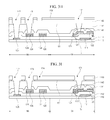
- FIG. 1 is a cross-sectional view illustrating an AH-IPS type LCD according to related art.
- the LCD includes an array substrate including a display region OA and a non-display region NA.
- a thin film transistor Tr In the array substrate, a thin film transistor Tr, a pixel electrode 52 connected to the thin film transistor Tr, and a common electrode 51 are formed on a substrate 10 .
- a gate line (not shown), a data line 20 , a gate pad 25 at an end of the gate line, and a data pad 26 at an end of the data line 20 are formed.
- the thin film transistor Tr includes a gate electrode 11 , a gate insulating layer 12 on the gate electrode 11 , an active layer 23 on the gate insulating layer 12 , and source and drain electrodes 22 and 21 on the active layer 23 .
- the thin film transistor Tr has an inverted staggered structure.
- the thin film transistor Tr may have a coplanar structure.
- First and second passivation layers 41 and 42 are formed on the thin film transistor Tr.
- the second passivation layer 42 functions as a planarization layer. When a planarization is not required, the second passivation layer 42 may be omitted.
- a common electrode 51 is formed on the second passivation layer 42 .
- a third passivation layer 43 is formed on the common electrode 51 and covers the common electrode 51 .
- a pixel electrode 52 is formed on the third passivation layer 43 .
- the array substrate for the LCD is manufactured with as many as 6 or 7 mask processes.
- the array substrate for the LCD is manufactured with one mask process to form the gate electrode 11 , one or two mask processes to form the active layer 23 and the source and drain electrodes 22 and 21 , one mask process to pattern the first and second passivation layers 41 and 42 , one mask process to form the common electrode 51 , one mask process to pattern the third passivation layer 43 , and one mask process to form the pixel electrode.
- the present invention is directed to a liquid crystal display device (LCD) that substantially obviates one or more of the problems due to limitations and disadvantages of the related art.
- LCD liquid crystal display device
- An advantage of the present invention is to provide an LCD that can reduce manufacturing processes and costs.
- a liquid crystal display device includes a gate electrode; a gate insulating layer on the gate electrode; an active layer on the gate insulating layer corresponding to the gate electrode; source and drain electrodes on the active layer; a first passivation layer on the source and drain electrodes; a common electrode on the first passivation layer; a second passivation layer on the common electrode, covering the common electrode, and having a separate region from the first passivation layer at a thickness of the common electrode; a pixel electrode on the second passivation layer and connected to the drain electrode through a drain contact hole; and a common line at a same layer as the pixel electrode and connected to the common electrode.
- a liquid crystal display device in another aspect, includes a gate electrode; a gate insulating layer on the gate electrode; an active layer on the gate insulating layer corresponding to the gate electrode; source and drain electrodes on the active layer; a first passivation layer on the source and drain electrodes; a second passivation layer on the first passivation layer; a common electrode on the second passivation layer and exposing a portion of the second passivation layer; a third passivation layer on the common electrode and having a separate region from the second passivation layer, wherein the common electrode is not located at the separate region; a pixel electrode on the third passivation layer and connected to the drain electrode through a drain contact hole; and a common line at a same layer as the pixel electrode and connected to the common electrode.
- a method of manufacturing a liquid crystal display device includes forming a gate line, a gate electrode and a gate pad on a substrate; forming a gate insulating layer on the gate line, the gate electrode and the gate pad; forming a data line, a source electrode, a drain electrode and a data pad on the gate insulating layer; forming a first passivation layer on the data line, the source electrode, the drain electrode and the data pad; forming a common layer on the first passivation layer; forming a second passivation layer on the common layer; first dry etching the second passivation layer; first wet etching the common layer exposed through the first dry-etched second passivation layer to form a common pattern; second dry etching the gate insulating layer, the first passivation layer and the second passivation layer; second wet etching the common pattern exposed through the second dry-etched second passivation layer to form a common electrode; and forming a pixel electrode and a common line on the second passivation
- FIG. 1 is a cross-sectional view illustrating an AH-IPS type LCD according to related art
- FIG. 2 is a cross-sectional view illustrating an AH-IPS type LCD according to an embodiment of the present invention.
- FIGS. 3A through 3K are cross-sectional views illustrating a method of manufacturing the LCD according to the embodiment of the present invention.
- FIG. 2 is a cross-sectional view illustrating an AH-IPS type LCD according to an embodiment of the present invention.
- the LCD includes an array substrate including a display region OA to display an image and a non-display region NA.
- the display region OA corresponds to a pixel region.
- a gate electrode 111 is formed in the pixel region on a substrate 110 , a gate insulating layer 112 is formed on the gate electrode 111 , and an active layer 123 is formed on the gate insulating layer 112 .
- a source electrode 122 and a drain electrode 121 are formed on the active layer 123 and spaced apart from each other.
- First and second passivation layers 141 and 142 are formed on the source and drain electrodes 122 and 121 .
- a common electrode 151 is formed on the second passivation layer 142 , and a third passivation layer 143 is formed on the common electrode 151 .
- a pixel electrode 152 is formed on the third passivation layer 143 .
- the gate electrode 111 , the active layer 123 , and the source and drain electrodes 122 and 121 form a thin film transistor Tr.
- a gate signal is applied to the gate electrode 111 , the thin film transistor Tr is turned on, and a data voltage supplied to the source electrode 122 is applied to the pixel electrode 152 through the thin film transistor Tr.
- the gate electrode 111 may extend from a gate line (not shown), and is supplied with a gate signal from a gate driver connected to a liquid crystal panel.
- the gate electrode 111 may be preferably made of an opaque material, thus may shield a channel of the active layer 123 from backlight.
- the source electrode 122 may extend from a data line 120 , and is supplied with a data voltage from a data driver connected to a liquid crystal panel.
- the drain electrode 121 is connected to the pixel electrode 152 .
- the source and drain electrodes 122 and 121 may be made of a single-layered structure using a metal material, for example, copper (Cu).
- the source and drain electrodes 122 and 121 may have a multiple-layered structure that includes a copper layer and other metal layer below the copper layer.
- the copper layer has a poor adhesive property to the active layer 123 , thus the other metal layer having a better adhesive property to the active layer 123 is formed below the copper layer.
- the active layer 123 may be made of amorphous silicon. Alternatively, poly silicon or oxide semiconductor may be used for the active layer 123 .
- the pixel electrode 152 may be made of a transparent conductive material, for example, ITO, IZO, ITZO or IGZO. Alternatively, the pixel electrode 152 may have a multiple-layered structure that uses different conductive materials. For example, the pixel electrode 152 may include a transparent conductive material layer and a metal material layer having a higher conductivity such as copper (Cu).
- a transparent conductive material for example, ITO, IZO, ITZO or IGZO.
- the pixel electrode 152 may have a multiple-layered structure that uses different conductive materials.
- the pixel electrode 152 may include a transparent conductive material layer and a metal material layer having a higher conductivity such as copper (Cu).
- the pixel electrode 152 may include a plurality of pixel patterns.
- the pixel electrode 152 may include a plurality of patterns in each pixel region.
- the pixel patterns may have a bar shape, and an opening may be formed between pixel patterns.
- a common line 153 is formed on the third passivation layer 143 .
- the common line 153 may be preferably formed at the same layer and of the same material as the pixel electrode 152 .
- the common line 153 is connected to the common electrode 151 and functions to transfer a common voltage to the common electrode 151 .
- the common electrode 151 faces the pixel electrode 152 with the third passivation layer 143 therebetween.
- the common electrode 151 has substantially a plate shape at the pixel region.
- the common electrode 151 may be made of a transparent conductive material, for example, ITO, IZO, ITZO or IGZO.
- the data line 120 In the non-display region NA, the data line 120 , the gate line, a data pad 126 at an end of the data line 120 , and a gate pad 125 at an end of the gate line are formed.
- a semiconductor pattern 124 formed of the same material as the active layer 123 may be formed below the data line 120 and the data pad 126 .
- a gate pad terminal 157 may be formed on the third passivation layer 143 and connected to the gate pad 125 through a gate pad contact hole 172 .
- a data pad terminal 158 may be formed on the third passivation layer 143 and connected to the data pad 126 through a data pad contact hole 173 .
- the gate pad terminal 157 and the data pad terminal 158 may be made of the same material as the pixel electrode 152 .
- FIGS. 3A through 3K are cross-sectional views illustrating a method of manufacturing the LCD according to the embodiment of the present invention.
- a first metal layer 111 a and a first photoresist layer are sequentially formed on a substrate 110 .
- a first photo mask M 1 including a transmissive portion O and a blocking portion C is located over the substrate 110 , and a light exposure is conducted to form a first photoresist pattern P 1 corresponding to the blocking portion C.
- the first photoresist pattern P 1 is formed on regions where a gate electrode, a gate line and a gate pad are formed.
- the first metal layer 111 a is etched using the first photoresist pattern P 1 as an etching mask to form the gate electrode 111 , the gate line, and the gate pad 125 .
- a gate insulating layer 112 is formed on the substrate 110 having the gate electrode 111 , the gate line and the gate pad 125 .
- a semiconductor layer 131 , a second metal layer 132 and a second photoresist layer are sequentially formed on the gate insulating layer 112 .
- a second photo mask M 2 including a transmissive portion O, a semi-transmissive portion H and a blocking portion C is located over the substrate 110 , and a light exposure is conducted to form a second photoresist pattern P 2 .
- the second photoresist pattern P 2 includes a first pattern P 2 a corresponding to the blocking portion C, and a second pattern P 2 b corresponding to the semi-transmissive portion H.
- the second pattern P 2 b has a thickness less than a thickness of the first pattern P 2 a.
- the first pattern P 2 a is formed at regions where a data line, source and drain electrodes and a data pad are formed.
- the second pattern P 2 b is formed at a region where a channel of an active layer between the source and drain electrodes is formed.
- the second metal layer 132 and the semiconductor layer 131 are etched using the second photoresist pattern P 2 as an etching mask to form a source-drain pattern, the data line 120 , the data pad 126 , and an active layer 123 below the source-drain pattern.
- a semiconductor pattern 124 is formed below the data line 120 and the data pad 126 .
- an ashing process is conducted for the second photoresist pattern P 2 to remove the second pattern P 2 b .
- the first pattern P 2 a remains after the ashing process.
- the source-drain pattern is etched using the ashed second photoresist pattern of the second pattern P 2 b as an etching mask to form the source and drain electrodes 122 and 121 spaced apart from each other. In this case, a portion of the active layer 123 between the source and drain electrodes 122 and 121 may be partially removed.
- a first passivation layer 141 , a second passivation layer 142 , a common metal layer 160 , and a third passivation layer 143 are sequentially formed on the substrate 110 having the source and drain electrodes 122 and 121 .
- the second passivation layer 142 functions as a planarization layer so that a top surface of the second passivation layer 142 is a substantially planar surface.
- the second passivation layer 142 may be omitted.
- the common layer 160 may be formed preferably at a thickness of about between 300 angstroms and 500 angstroms.
- a third photoresist layer (not shown) is formed on the third passivation layer 143 , and then a light exposure is conducted using a third photo mask M 3 including a transmissive portion O, a semi-transmissive portion H and a blocking portion C. Accordingly, a third photoresist pattern P 3 is formed.
- the third photoresist pattern P 3 includes a third pattern P 3 a corresponding to the blocking portion C, and a fourth pattern P 3 b corresponding to the semi-transmissive portion H.
- the fourth pattern P 3 b has a thickness less than a thickness of the third pattern P 3 a.
- the fourth pattern P 3 b is formed at a region where a common contact hole is formed.
- the removed portions of the third photoresist pattern i.e., openings
- the third pattern P 3 a is formed at regions other than the fourth pattern P 3 b and the removed portion of the third photoresist pattern P 3 .
- the third passivation layer 143 is etched using the third photoresist pattern P 3 as an etching mask to form holes in the third passivation layer 143 that expose the common layer 160 .
- This etching may be preferably a dry etching.
- the dry etching does not influence the common layer 160 .
- the dry etching is an anisotropic etching.
- the common layer 160 is etched using the third photoresist pattern P 3 as an etching mask to form a common pattern 161 .
- This etching may be preferably a wet etching, and the wet etching may preferably use an etching solution including an oxalic acid.
- the wet etching is an isotropic etching. Since the common layer 160 is wet etched, the common pattern 161 has an under cut shape such that the common pattern 161 has a recessed side surface with respect to a corresponding side surface of the third passivation layer 143 .
- the second passivation layer 142 , the first passivation layer 141 , and the gate insulating layer 112 are etched using the common pattern 161 as an etching mask.
- This etching may be preferably a dry etching, and the dry etching does not influence the common pattern 161 .
- the third passivation layer 143 may be also etched, and the third photoresist pattern may be ashed.
- an area of the common layer 160 exposed in the dry etching of the third passivation layer 143 is determined by a width of the etched portion (i.e., the opening) of the third passivation layer 143 , and a portion of the second passivation layer 142 exposed in the wet etching of the common layer 160 is dry etched. Accordingly, by adjusting the etched area of the common layer 160 (i.e., the area of the common pattern 161 ), the second passivation layer 142 is etched at a desired width.
- a drain contact hole 171 exposing the drain electrode 121 , a gate pad contact hole 172 exposing the gate pad 125 , and a data pad contact hole 173 exposing the data pad 126 are formed.
- the fourth pattern P 3 b is removed, and a portion of the third passivation layer 143 below the fourth pattern P 3 b is partially removed.
- the partially-removed portion of the third passivation layer 143 has a thickness less than a thickness of other portion of the third passivation layer 143 .
- a side surface of the third passivation layer 143 surrounding each of the contact holes 171 , 172 and 173 is recessed with respect to the corresponding side surface of the second passivation layer 142 .
- the side surface of the third passivation layer 143 is recessed by 2 ⁇ m or 3 ⁇ m with respect to the corresponding side surface of the second passivation layer 142 . This is because the etching of the second passivation layer 142 is restricted by the common pattern 161 .
- the common pattern 161 is exposed to outside through the third passivation layer 143 .
- the common pattern 161 protrudes with respect to the side surface of the third passivation layer 143 .
- the wet etching is conducted such that a side surface of the common electrode 151 is recessed with respect to the corresponding side surfaces of the third and second passivation layers 143 and 142 .
- the common electrode 151 has an under cut shape between the third passivation layer 143 and the second passivation layer 142 .
- a pixel layer 165 and a fourth photoresist layer are formed on the substrate 110 having the common electrode 151 .
- a fourth photo mask M 4 including a transmissive portion O and a blocking portion C is located over the substrate 110 , and a light exposure is conducted to form a fourth photoresist pattern P 4 .
- the pixel layer 165 is formed along the surfaces of the third passivation layer 143 and the second passivation layer 142 , and contacts the common electrode 151 , the drain electrode 121 , the gate pad 125 and the data pad 126 .
- the pixel layer 165 does not contact the common electrode 151 at the contact holes 171 , 172 and 173 and the pixel layer 165 and the common electrode 151 are separated from each other. In other words, the common electrode 151 and the pixel layer 165 are not short-circuited therebetween at the contact holes 171 , 172 and 173 .
- the common layer 160 i.e., common electrode 151 preferably has a thickness between 300 angstroms and 500 angstroms.
- the second passivation layer 142 and the third passivation layer 143 are separated over 500 angstroms.
- the pixel layer 165 might be disconnected at the separate portion between the second and third passivation layers 142 and 143 , thus electrical disconnections of a pixel electrode, a common line, a gate pad terminal and a data pad terminal may occur.
- the common electrode 151 has a thickness below 300 angstroms, the second passivation layer 142 and the third passivation layer 143 are separated below 300 angstroms. In this case, the pixel layer 165 might not be disconnected at the separate portion between the second and third passivation layers 142 and 143 . However, resistance of the common electrode 151 may increase. As a result, power consumption may increase, and electrical disconnection of the common electrode 151 may occur.
- the common layer 160 has the thickness of about between 300 angstroms and 500 angstroms.
- the pixel layer 165 is etched using the fourth photoresist pattern P 4 as an etching mask. Accordingly, the pixel electrode 152 contacting the drain electrode 121 through the drain contact hole 171 , the common line 153 contacting the common electrode 151 through the common contact hole 174 , the gate pad terminal 157 contacting the gate pad 125 through the gate pad contact hole 172 , and the data pad terminal 158 contacting the data pad 126 through the data pad contact hole 173 are formed. Then, the fourth photoresist pattern P 4 is removed.
- the array substrate for the LCD can be manufactured.
- the array substrate is coupled with an opposing substrate, for example, a color filter substrate with a liquid crystal layer therebetween, thus the LCD can be manufactured.
- the array substrate can be manufactured with four mask processes. Particularly, by forming the common electrode having an under cut shape, the processes after forming the thin film transistor are completed with two mask processes. Therefore, manufacturing processes of AH-IPS type LCD can be performed efficiently and manufacturing costs can be reduced.
Abstract
Description
Claims (14)
Priority Applications (1)
| Application Number | Priority Date | Filing Date | Title |
|---|---|---|---|
| US14/919,633 US9236399B1 (en) | 2013-12-31 | 2015-10-21 | Liquid crystal display device and manufacturing method thereof |
Applications Claiming Priority (2)
| Application Number | Priority Date | Filing Date | Title |
|---|---|---|---|
| KR1020130169083A KR102132445B1 (en) | 2013-12-31 | 2013-12-31 | Liquid Crystal Display Panel And Manufacturing Method Of The Same |
| KR10-2013-0169083 | 2013-12-31 |
Related Child Applications (1)
| Application Number | Title | Priority Date | Filing Date |
|---|---|---|---|
| US14/919,633 Division US9236399B1 (en) | 2013-12-31 | 2015-10-21 | Liquid crystal display device and manufacturing method thereof |
Publications (2)
| Publication Number | Publication Date |
|---|---|
| US20150187817A1 US20150187817A1 (en) | 2015-07-02 |
| US9219080B2 true US9219080B2 (en) | 2015-12-22 |
Family
ID=53482747
Family Applications (2)
| Application Number | Title | Priority Date | Filing Date |
|---|---|---|---|
| US14/584,958 Active US9219080B2 (en) | 2013-12-31 | 2014-12-29 | Liquid crystal display device and manufacturing method thereof |
| US14/919,633 Active US9236399B1 (en) | 2013-12-31 | 2015-10-21 | Liquid crystal display device and manufacturing method thereof |
Family Applications After (1)
| Application Number | Title | Priority Date | Filing Date |
|---|---|---|---|
| US14/919,633 Active US9236399B1 (en) | 2013-12-31 | 2015-10-21 | Liquid crystal display device and manufacturing method thereof |
Country Status (3)
| Country | Link |
|---|---|
| US (2) | US9219080B2 (en) |
| KR (1) | KR102132445B1 (en) |
| CN (1) | CN104749842B (en) |
Families Citing this family (12)
| Publication number | Priority date | Publication date | Assignee | Title |
|---|---|---|---|---|
| CN104766819B (en) * | 2014-01-06 | 2017-12-08 | 瀚宇彩晶股份有限公司 | Picture element substrate and its manufacture method |
| KR102322015B1 (en) * | 2015-04-07 | 2021-11-05 | 삼성디스플레이 주식회사 | Manufacturing method of thin-film transistor array substrate and thin-film transistor array substrate thereof |
| CN105116642B (en) * | 2015-09-24 | 2018-07-17 | 京东方科技集团股份有限公司 | Array substrate and preparation method thereof, display device |
| CN105448933B (en) * | 2015-11-24 | 2018-10-30 | 深圳市华星光电技术有限公司 | For the array substrate and preparation method thereof in liquid crystal display panel |
| KR102494779B1 (en) * | 2015-12-22 | 2023-02-02 | 엘지디스플레이 주식회사 | Liquid crystal display with touch |
| KR102454383B1 (en) * | 2015-12-28 | 2022-10-17 | 엘지디스플레이 주식회사 | Fringe Field Switching Type Liquid Crystal Dispaly |
| CN105487285B (en) * | 2016-02-01 | 2018-09-14 | 深圳市华星光电技术有限公司 | The preparation method of array substrate and array substrate |
| KR102555392B1 (en) * | 2016-03-18 | 2023-07-14 | 삼성디스플레이 주식회사 | Display device and fabricating method thereof |
| JP2019066719A (en) * | 2017-10-03 | 2019-04-25 | シャープ株式会社 | Display panel |
| CN110061058A (en) * | 2018-04-17 | 2019-07-26 | 京东方科技集团股份有限公司 | Array substrate and preparation method thereof, display device |
| CN110707047B (en) * | 2019-09-17 | 2022-07-01 | 昆山龙腾光电股份有限公司 | Array substrate, manufacturing method and display panel |
| CN111446260B (en) * | 2020-03-31 | 2023-07-21 | 京东方科技集团股份有限公司 | Array substrate, preparation method thereof and display device |
Citations (10)
| Publication number | Priority date | Publication date | Assignee | Title |
|---|---|---|---|---|
| US20060192906A1 (en) * | 2005-02-25 | 2006-08-31 | Samsung Electronics Co., Ltd. | Thin film transistor array panel and manufacturing method thereof |
| US20110157039A1 (en) * | 2009-12-28 | 2011-06-30 | Hee-Sun Shin | Liquid crystal display device and method of fabricating the same |
| US20120176561A1 (en) * | 2011-01-10 | 2012-07-12 | Gee-Bum Kim | Liquid crystal display |
| US20130309821A1 (en) * | 2009-06-03 | 2013-11-21 | Samsung Display Co., Ltd. | Thin film transistor array substrate for a display panel and a method for manufacturing a thin film transistor array substrate for a display panel |
| US20150062521A1 (en) * | 2013-09-02 | 2015-03-05 | Samsung Display Co., Ltd. | Liquid crystal display |
| US20150092136A1 (en) * | 2013-09-30 | 2015-04-02 | Lg Display Co., Ltd. | Liquid crystal display device and method for manufacturing the same |
| US20150155310A1 (en) * | 2013-12-02 | 2015-06-04 | Lg Display Co., Ltd. | Thin film transistor substrate having metal oxide semiconductor and manufacturing the same |
| US20150162251A1 (en) * | 2013-12-06 | 2015-06-11 | Samsung Display Co., Ltd. | Display device and manufacturing method thereof |
| US20150171111A1 (en) * | 2013-12-16 | 2015-06-18 | Samsung Display Co., Ltd. | Thin film transistor array panel and method of manufacturing the same |
| US20150214253A1 (en) * | 2013-05-23 | 2015-07-30 | Hefei Boe Optoelectronics Technology Co. Ltd | Array substrate, manufacturing method thereof and display device |
Family Cites Families (10)
| Publication number | Priority date | Publication date | Assignee | Title |
|---|---|---|---|---|
| US20050260804A1 (en) * | 2004-05-24 | 2005-11-24 | Tae-Wook Kang | Semiconductor device and method of fabricating the same |
| KR101090249B1 (en) * | 2004-10-06 | 2011-12-06 | 삼성전자주식회사 | Method for manufacturing thin film transistor array panel |
| KR101225440B1 (en) * | 2005-06-30 | 2013-01-25 | 엘지디스플레이 주식회사 | Liquid crystal display and fabricating method thereof |
| KR101250319B1 (en) * | 2009-10-06 | 2013-04-03 | 엘지디스플레이 주식회사 | Fringe field switching mode liquid crystal display device and Method of fabricating the same |
| JP5280988B2 (en) * | 2009-11-09 | 2013-09-04 | 株式会社ジャパンディスプレイ | Manufacturing method of liquid crystal display device |
| KR101333614B1 (en) * | 2010-06-25 | 2013-11-27 | 엘지디스플레이 주식회사 | Liquid crystal display device |
| KR101394938B1 (en) * | 2011-05-03 | 2014-05-14 | 엘지디스플레이 주식회사 | Thin film transistor substrate and method of fabricating the same |
| KR101870986B1 (en) * | 2011-09-19 | 2018-06-26 | 엘지디스플레이 주식회사 | Method for fabricating thin film transistor array substrate |
| KR101894328B1 (en) * | 2011-10-06 | 2018-09-03 | 엘지디스플레이 주식회사 | Thin film transistor substrate and method of fabricating the same |
| KR101923717B1 (en) * | 2012-05-24 | 2018-11-30 | 엘지디스플레이 주식회사 | Array substrate for liquid crystal display and manufacturing method of the same |
-
2013
- 2013-12-31 KR KR1020130169083A patent/KR102132445B1/en active IP Right Grant
-
2014
- 2014-12-24 CN CN201410858289.0A patent/CN104749842B/en active Active
- 2014-12-29 US US14/584,958 patent/US9219080B2/en active Active
-
2015
- 2015-10-21 US US14/919,633 patent/US9236399B1/en active Active
Patent Citations (10)
| Publication number | Priority date | Publication date | Assignee | Title |
|---|---|---|---|---|
| US20060192906A1 (en) * | 2005-02-25 | 2006-08-31 | Samsung Electronics Co., Ltd. | Thin film transistor array panel and manufacturing method thereof |
| US20130309821A1 (en) * | 2009-06-03 | 2013-11-21 | Samsung Display Co., Ltd. | Thin film transistor array substrate for a display panel and a method for manufacturing a thin film transistor array substrate for a display panel |
| US20110157039A1 (en) * | 2009-12-28 | 2011-06-30 | Hee-Sun Shin | Liquid crystal display device and method of fabricating the same |
| US20120176561A1 (en) * | 2011-01-10 | 2012-07-12 | Gee-Bum Kim | Liquid crystal display |
| US20150214253A1 (en) * | 2013-05-23 | 2015-07-30 | Hefei Boe Optoelectronics Technology Co. Ltd | Array substrate, manufacturing method thereof and display device |
| US20150062521A1 (en) * | 2013-09-02 | 2015-03-05 | Samsung Display Co., Ltd. | Liquid crystal display |
| US20150092136A1 (en) * | 2013-09-30 | 2015-04-02 | Lg Display Co., Ltd. | Liquid crystal display device and method for manufacturing the same |
| US20150155310A1 (en) * | 2013-12-02 | 2015-06-04 | Lg Display Co., Ltd. | Thin film transistor substrate having metal oxide semiconductor and manufacturing the same |
| US20150162251A1 (en) * | 2013-12-06 | 2015-06-11 | Samsung Display Co., Ltd. | Display device and manufacturing method thereof |
| US20150171111A1 (en) * | 2013-12-16 | 2015-06-18 | Samsung Display Co., Ltd. | Thin film transistor array panel and method of manufacturing the same |
Also Published As
| Publication number | Publication date |
|---|---|
| KR20150079089A (en) | 2015-07-08 |
| US9236399B1 (en) | 2016-01-12 |
| CN104749842B (en) | 2018-03-09 |
| US20150187817A1 (en) | 2015-07-02 |
| CN104749842A (en) | 2015-07-01 |
| KR102132445B1 (en) | 2020-07-09 |
Similar Documents
| Publication | Publication Date | Title |
|---|---|---|
| US9236399B1 (en) | Liquid crystal display device and manufacturing method thereof | |
| US8933460B2 (en) | Array substrate for fringe field switching mode liquid crystal display device | |
| US8895987B2 (en) | Array substrate for fringe field switching mode liquid crystal display device and method of fabricating the same | |
| US8045078B2 (en) | Array substrate for liquid crystal display device and method of fabricating the same | |
| US9768275B2 (en) | Array substrate for fringe field switching mode liquid crystal display device and method of fabricating the same | |
| US7830464B2 (en) | Array substrate for fringe field switching mode liquid crystal display device and method of fabricating the same | |
| US8379177B2 (en) | Array substrate for fringe field switching mode liquid crystal display device and method of fabricating the same | |
| US10809559B2 (en) | Liquid crystal display device and method of fabricating the same | |
| US8643799B2 (en) | TFT-LCD array substrate and manufacturing method thereof | |
| US7943937B2 (en) | Array substrate for liquid crystal display device and method of fabricating the same | |
| US8803147B2 (en) | Array substrate for fringe field switching mode liquid crystal display device and method of manufacturing the same | |
| KR101870986B1 (en) | Method for fabricating thin film transistor array substrate | |
| EP3091568B1 (en) | Array substrate, manufacturing method therefor, display device and electronic product | |
| US8502945B2 (en) | Array substrate of fringe field switching mode liquid crystal display panel and method of manufacturing the same | |
| KR20070000893A (en) | Liquid crystal display apparatus of horizontal electronic field applying type and fabricating method thereof | |
| US7884912B2 (en) | Liquid crystal display device | |
| US20070153206A1 (en) | Array substrate for in-plane switching mode liquid crystal display device and method of manufacturing the same | |
| KR20110118999A (en) | Fringe field switching mode liquid crystal display device and the method for fabricating the same | |
| JP2015031714A (en) | Thin film transistor array substrate and method for manufacturing the same | |
| KR20110053034A (en) | Liquid crystal display device for cot type and method for manufacturing the same | |
| KR20110072433A (en) | Method for fabricating liquid crystal display device | |
| US7961284B2 (en) | Liquid crystal display and method for manufacturing the same | |
| KR101374997B1 (en) | Liquid crystal display device and method of fabricating the same | |
| KR101953593B1 (en) | Liquid crystal display device and method of fabricating the same | |
| KR101852632B1 (en) | Thin film transistor array substrate and method for fabricating the same |
Legal Events
| Date | Code | Title | Description |
|---|---|---|---|
| AS | Assignment |
Owner name: LG DISPLAY CO., LTD., KOREA, REPUBLIC OF Free format text: ASSIGNMENT OF ASSIGNORS INTEREST;ASSIGNORS:KIM, YONG-IL;KIM, MIN-JOO;REEL/FRAME:035199/0042 Effective date: 20150310 |
|
| STCF | Information on status: patent grant |
Free format text: PATENTED CASE |
|
| MAFP | Maintenance fee payment |
Free format text: PAYMENT OF MAINTENANCE FEE, 4TH YEAR, LARGE ENTITY (ORIGINAL EVENT CODE: M1551); ENTITY STATUS OF PATENT OWNER: LARGE ENTITY Year of fee payment: 4 |
|
| MAFP | Maintenance fee payment |
Free format text: PAYMENT OF MAINTENANCE FEE, 8TH YEAR, LARGE ENTITY (ORIGINAL EVENT CODE: M1552); ENTITY STATUS OF PATENT OWNER: LARGE ENTITY Year of fee payment: 8 |