US9140895B2 - Imaging apparatus and imaging method for obtaining images fro electromagnetic waves - Google Patents
Imaging apparatus and imaging method for obtaining images fro electromagnetic waves Download PDFInfo
- Publication number
- US9140895B2 US9140895B2 US13/655,145 US201213655145A US9140895B2 US 9140895 B2 US9140895 B2 US 9140895B2 US 201213655145 A US201213655145 A US 201213655145A US 9140895 B2 US9140895 B2 US 9140895B2
- Authority
- US
- United States
- Prior art keywords
- transmission
- section
- imaging
- actuator
- moving slit
- Prior art date
- Legal status (The legal status is an assumption and is not a legal conclusion. Google has not performed a legal analysis and makes no representation as to the accuracy of the status listed.)
- Expired - Fee Related, expires
Links
- 238000003384 imaging method Methods 0.000 title claims abstract description 168
- 230000005540 biological transmission Effects 0.000 claims abstract description 176
- 230000003287 optical effect Effects 0.000 claims abstract description 69
- 230000000903 blocking effect Effects 0.000 claims abstract description 44
- 239000004020 conductor Substances 0.000 claims description 6
- 230000014759 maintenance of location Effects 0.000 claims description 6
- 239000011347 resin Substances 0.000 claims description 4
- 229920005989 resin Polymers 0.000 claims description 4
- 229920000642 polymer Polymers 0.000 claims description 3
- 230000011664 signaling Effects 0.000 abstract description 4
- 230000033001 locomotion Effects 0.000 description 21
- 238000001514 detection method Methods 0.000 description 16
- 238000010586 diagram Methods 0.000 description 16
- 230000008859 change Effects 0.000 description 13
- 239000007787 solid Substances 0.000 description 10
- 230000004907 flux Effects 0.000 description 9
- 238000003331 infrared imaging Methods 0.000 description 9
- 238000005549 size reduction Methods 0.000 description 9
- 238000001931 thermography Methods 0.000 description 9
- 230000008901 benefit Effects 0.000 description 8
- 230000000717 retained effect Effects 0.000 description 8
- 239000005083 Zinc sulfide Substances 0.000 description 6
- 238000000034 method Methods 0.000 description 6
- 230000004044 response Effects 0.000 description 6
- 229910052984 zinc sulfide Inorganic materials 0.000 description 6
- 239000006059 cover glass Substances 0.000 description 5
- 230000008569 process Effects 0.000 description 5
- 230000035945 sensitivity Effects 0.000 description 5
- 230000005684 electric field Effects 0.000 description 4
- 229910052751 metal Inorganic materials 0.000 description 4
- 239000002184 metal Substances 0.000 description 4
- 230000004048 modification Effects 0.000 description 4
- 238000012986 modification Methods 0.000 description 4
- 229910001935 vanadium oxide Inorganic materials 0.000 description 4
- 229910052782 aluminium Inorganic materials 0.000 description 3
- XAGFODPZIPBFFR-UHFFFAOYSA-N aluminium Chemical compound [Al] XAGFODPZIPBFFR-UHFFFAOYSA-N 0.000 description 3
- 238000005530 etching Methods 0.000 description 3
- 230000010287 polarization Effects 0.000 description 3
- 230000005855 radiation Effects 0.000 description 3
- 238000002834 transmittance Methods 0.000 description 3
- RYGMFSIKBFXOCR-UHFFFAOYSA-N Copper Chemical compound [Cu] RYGMFSIKBFXOCR-UHFFFAOYSA-N 0.000 description 2
- 229910052802 copper Inorganic materials 0.000 description 2
- 239000010949 copper Substances 0.000 description 2
- 230000000694 effects Effects 0.000 description 2
- 229910052732 germanium Inorganic materials 0.000 description 2
- GNPVGFCGXDBREM-UHFFFAOYSA-N germanium atom Chemical compound [Ge] GNPVGFCGXDBREM-UHFFFAOYSA-N 0.000 description 2
- 239000000463 material Substances 0.000 description 2
- 230000005499 meniscus Effects 0.000 description 2
- 239000004065 semiconductor Substances 0.000 description 2
- DRDVZXDWVBGGMH-UHFFFAOYSA-N zinc;sulfide Chemical compound [S-2].[Zn+2] DRDVZXDWVBGGMH-UHFFFAOYSA-N 0.000 description 2
- XHCLAFWTIXFWPH-UHFFFAOYSA-N [O-2].[O-2].[O-2].[O-2].[O-2].[V+5].[V+5] Chemical compound [O-2].[O-2].[O-2].[O-2].[O-2].[V+5].[V+5] XHCLAFWTIXFWPH-UHFFFAOYSA-N 0.000 description 1
- 230000004075 alteration Effects 0.000 description 1
- 238000003705 background correction Methods 0.000 description 1
- 230000036760 body temperature Effects 0.000 description 1
- 230000007547 defect Effects 0.000 description 1
- 230000003467 diminishing effect Effects 0.000 description 1
- 238000009826 distribution Methods 0.000 description 1
- 239000000428 dust Substances 0.000 description 1
- 239000011796 hollow space material Substances 0.000 description 1
- 238000009413 insulation Methods 0.000 description 1
- 230000005415 magnetization Effects 0.000 description 1
- 230000007257 malfunction Effects 0.000 description 1
- 238000004519 manufacturing process Methods 0.000 description 1
- 230000004297 night vision Effects 0.000 description 1
- 230000009467 reduction Effects 0.000 description 1
- 229910052710 silicon Inorganic materials 0.000 description 1
- 239000010703 silicon Substances 0.000 description 1
- 238000004544 sputter deposition Methods 0.000 description 1
- 238000007740 vapor deposition Methods 0.000 description 1
Images


Classifications
-
- G—PHYSICS
- G02—OPTICS
- G02B—OPTICAL ELEMENTS, SYSTEMS OR APPARATUS
- G02B26/00—Optical devices or arrangements for the control of light using movable or deformable optical elements
- G02B26/02—Optical devices or arrangements for the control of light using movable or deformable optical elements for controlling the intensity of light
- G02B26/04—Optical devices or arrangements for the control of light using movable or deformable optical elements for controlling the intensity of light by periodically varying the intensity of light, e.g. using choppers
-
- G—PHYSICS
- G01—MEASURING; TESTING
- G01J—MEASUREMENT OF INTENSITY, VELOCITY, SPECTRAL CONTENT, POLARISATION, PHASE OR PULSE CHARACTERISTICS OF INFRARED, VISIBLE OR ULTRAVIOLET LIGHT; COLORIMETRY; RADIATION PYROMETRY
- G01J5/00—Radiation pyrometry, e.g. infrared or optical thermometry
- G01J5/02—Constructional details
- G01J5/08—Optical arrangements
- G01J5/0803—Arrangements for time-dependent attenuation of radiation signals
- G01J5/0804—Shutters
-
- G—PHYSICS
- G01—MEASURING; TESTING
- G01J—MEASUREMENT OF INTENSITY, VELOCITY, SPECTRAL CONTENT, POLARISATION, PHASE OR PULSE CHARACTERISTICS OF INFRARED, VISIBLE OR ULTRAVIOLET LIGHT; COLORIMETRY; RADIATION PYROMETRY
- G01J5/00—Radiation pyrometry, e.g. infrared or optical thermometry
- G01J5/02—Constructional details
- G01J5/08—Optical arrangements
- G01J5/0803—Arrangements for time-dependent attenuation of radiation signals
- G01J5/0805—Means for chopping radiation
-
- G01J5/0834—
-
- G—PHYSICS
- G01—MEASURING; TESTING
- G01J—MEASUREMENT OF INTENSITY, VELOCITY, SPECTRAL CONTENT, POLARISATION, PHASE OR PULSE CHARACTERISTICS OF INFRARED, VISIBLE OR ULTRAVIOLET LIGHT; COLORIMETRY; RADIATION PYROMETRY
- G01J5/00—Radiation pyrometry, e.g. infrared or optical thermometry
- G01J5/10—Radiation pyrometry, e.g. infrared or optical thermometry using electric radiation detectors
- G01J5/34—Radiation pyrometry, e.g. infrared or optical thermometry using electric radiation detectors using capacitors, e.g. pyroelectric capacitors
-
- G01J5/62—
-
- G—PHYSICS
- G01—MEASURING; TESTING
- G01J—MEASUREMENT OF INTENSITY, VELOCITY, SPECTRAL CONTENT, POLARISATION, PHASE OR PULSE CHARACTERISTICS OF INFRARED, VISIBLE OR ULTRAVIOLET LIGHT; COLORIMETRY; RADIATION PYROMETRY
- G01J5/00—Radiation pyrometry, e.g. infrared or optical thermometry
- G01J2005/0077—Imaging
Definitions
- the present disclosure relates to an imaging apparatus suitable for obtaining images from electromagnetic waves such as infrared rays.
- infrared imaging apparatus e.g., thermal imaging apparatus, which images a target object using infrared sensors each being an infrared detection pixel, and measures the temperature of the object.
- thermal imaging apparatus which images a target object using infrared sensors each being an infrared detection pixel, and measures the temperature of the object.
- This infrared imaging apparatus is configured by a lens and an imaging element, which are each a very expensive device.
- the lens for use is expected to be a very expensive group of lenses made of Ge (germanium), ZnS (zinc sulfide), Si (silicon), or others with an excellent transmittance in the infrared wavelength region.
- a piece of Ge lens costs 10,000 to 50,000 yen, and the lens is used in a set of two to five pieces. Therefore, only the lenses cost 20,000 to 250,000 yen in total although the price is depending on the expected resolution.
- the current Ge lens uses germanium being a rare metal and hardly on the market, and thus the price of the material is very expensive like 50,000 to 180,000 yen/Kg.
- ZnS zinc sulfide
- ZnS is indeed cheaper in price, but is poor in productivity in terms of processing. This results in a higher processing cost, and the resulting ZnS lens costs almost the same as a Ge lens.
- the price is less expensive than a Ge lens, but is not suitable for use with thermography because of a reduced transmittance in the far infrared radiation area (8 to 14 ⁇ m).
- a lens not using a rare metal being low in cost, and having a transmittance remaining the same even in the far infrared radiation area is not yet on the market. That is, as described above, an inexpensive lens is not yet proposed for use in an imaging apparatus using general terahertz waves, i.e., typically far infrared thermography.
- the imaging element in use is called microbolometer, and is in the hollow structure of supporting each VOx (vanadium oxide)-made pixel in the hollow space.
- the infrared sensors are each of a thermal type, and VOx has a low temperature coefficient resistance (TCR) ⁇ .
- TCR temperature coefficient resistance
- S/N ratio Signal-to-Noise ratio
- the microbolometer has been the device being very poor in productivity, and being very expensive in price.
- the microbolometer is expected to be manufactured by sputtering, vapor deposition, or others in a process different from the semiconductor process of manufacturing wiring patterns and circuits. This is because the etching process for the hollow structure does not work well with the semiconductor process, thereby also causing the price increase of the microbolometer.
- the infrared imaging apparatus in the high-cost structure as such is priced for about 600,000 yen if it is low in resolution, and for about 9,000,000 yen if it is high in resolution. Therefore, the infrared imaging apparatus currently available on the market is only for industrial use, and the market is not yet created for the infrared imaging apparatus for consumer use.
- the imaging apparatus using terahertz waves not for far infrared thermography is under the circumstances similarly to the thermal imaging apparatus, and is sometimes more expensive than the thermal imaging apparatus.
- the current far infrared thermography has a limited range of use, e.g., temperature management for industrial-use facilities, temperature detection of objects for security/safety measures, night vision system equipped in luxury vehicles for night-time human detection, and the body temperature detection for medical use.
- the number of units of the imaging apparatus shipped globally has remained at about 10,000 to 20,000 per year.
- the fact is that the imaging apparatus using terahertz waves is barely produced.
- the use of a pyroelectric element is a possibility, for example.
- the examples of using the pyroelectric element for far-infrared detection include automatic doors, air conditioners, and human detection sensors for human detection in front of television.
- the issue here is that, in the previous infrared sensor using the pyroelectric element as such, the number of pyroelectric elements in use is one to four or so.
- the infrared sensor is thus a far cry from subject imaging, and is capable only of detecting if anyone cut across in front thereof.
- the output of the pyroelectric element shows a change depending on a change of temperature, and thus the pyroelectric element does not detect an object if the object is not moving.
- an optical chopper is expected to provide a chopper function, i.e., periodically releasing and blocking the entire surface of the imager.
- an optical chopper 101 is disposed as a light-shielding member in front of an imager (imaging element) 103 using a pyroelectric element.
- the optical chopper 101 is circular in shape, and is formed with apertures 102 .
- the optical chopper 101 is rotated about the optical axis, i.e., the center line indicated by alternate long and short dashed lines, so that light L is allowed to reach the imager 103 or is blocked before reaching the imager 103 .
- the optical axis i.e., the center line indicated by alternate long and short dashed lines
- the optical chopper 101 itself is large in size as is evident from FIG. 16 , and because the optical chopper 101 is to be rotated, a very large space is expected comparing to the area from which the light L comes for imaging.
- An imaging apparatus includes an imaging element section configured to include a plurality of pixels, an imaging optical system configured to form an image on the imaging element section, the image being formed by an electromagnetic wave from the outside, a transmission/block section configured to transmit and block the electromagnetic wave to/against the imaging element section, the transmission/block section being disposed at an aperture stop position in the imaging optical system, an actuator configured to drive the transmission/block section to move back and forth to be changed in state between transmission and blocking, and an output section configured to produce an image signal output, the image signal output being differential signaling between a pixel output from the imaging element section when the transmission/block section is in the state of transmission, and a pixel output from the imaging element section when the transmission/block section is in the state of blocking.
- An imaging method is for an imaging apparatus that includes an imaging element section configured to include a plurality of pixels, and an imaging optical system configured to form an image on the imaging element section, the image being formed by an electromagnetic wave from the outside.
- the method includes driving a transmission/block section to move back and forth to be changed in state between transmission and blocking, the transmission/block section being disposed at an aperture stop position in the imaging optical system, and the transmission/block section transmitting and blocking the electromagnetic wave to/against the pixels in the imaging element section, and producing an image signal output, the image signal output being differential signaling between a pixel output from the imaging element section when the transmission/block section is in the state of transmission, and a pixel output from the imaging element section when the transmission/block section is in the state of blocking.
- the transmission/block section configured to transmit and block the electromagnetic waves to/against the pixels in the imaging element section is provided at the aperture stop position in the imaging optical system.
- the aperture stop position is where incident luminous fluxes coming from each angle of view mainly gather.
- the aperture stop position is in the vicinity of the area where the aperture stops are formed in the imaging optical system, and is where incident luminous fluxes coming from each angle of view mainly gather.
- the expression of “disposed at the aperture stop position” means that the transmission/block section is disposed to be adjacent to the members each being the aperture stop not via any other optical element, or a part of the transmission/block section is integrated with the aperture-stop members.
- the small-sized transmission/block section can transmit/block electromagnetic waves to/against the imaging element section. This realizes the considerable size reduction of the imaging apparatus in which the imaging element section is a pyroelectric element, for example.
- FIGS. 1A and 1B are each a diagram illustrating an imaging optical system according to a first embodiment of the present disclosure
- FIG. 2 is a diagram illustrating a moving slit plate in the first embodiment
- FIGS. 3A to 3C are each a diagram illustrating the layout in which the moving slit plate in the first embodiment is disposed at an aperture stop position;
- FIG. 4 is a block diagram showing the configuration of an imaging apparatus in the first embodiment
- FIG. 5 is a diagram illustrating an output signal from a pyroelectric element in the first embodiment
- FIGS. 6A and 6B are each a diagram illustrating an imaging optical system in a second embodiment
- FIGS. 7A and 7B are each a diagram illustrating an imaging optical system in a third embodiment
- FIGS. 8A and 8B are each a diagram illustrating an imaging optical system in a fourth embodiment
- FIGS. 9A and 9B are each a diagram illustrating an imaging optical system in a fifth embodiment
- FIG. 10 is a diagram illustrating a bimorph piezo element
- FIG. 11 is a diagram illustrating actuators using the bimorph piezo elements
- FIG. 12 is a diagram illustrating the Lorentz force
- FIGS. 13A and 13B are each a diagram illustrating a Lorentz force actuator
- FIGS. 14A and 14B are each a diagram illustrating the chassis configuration in the embodiments.
- FIGS. 15A and 15B are each a diagram illustrating the layout of actuators in the chassis in the embodiments.
- FIG. 16 is a diagram illustrating a pervious imaging apparatus using an optical chopper.
- Imaging apparatuses according to the embodiments are each an infrared imaging apparatus using a pyroelectric sensor as an image sensor.
- FIGS. 1A and 1B An imaging apparatus in a first embodiment is described. First of all, an imaging optical system is described by referring to FIGS. 1A and 1B .
- three lenses of a first lens 11 , a second lens 12 , and a third lens 14 are provided from the object side to the image surface side.
- the first and third lenses 11 and 14 are each a plano-convex lens, and the second lens 12 is a meniscus lens.
- aperture stops 13 are provided between any two of the first to third lenses 11 to 14 .
- FIGS. 1A and 1B shows the configuration in which the aperture stops 13 are provided between the second and third lenses 12 and 14 .
- a fixed slit plate 20 and a moving slit plate 30 next thereto are provided at the position adjacent to the aperture stops 13 , i.e., aperture stop position.
- the fixed slit plate 20 and the moving slit plate 30 configure a transmission/block section SH.
- incoming light (electromagnetic waves) guided thereby is directed to an image sensor 16 via a cover glass 15 .
- the components in the imaging optical system i.e., the first, second, and third lenses 11 , 12 , and 14 , the aperture stops 13 , the fixed slit plate 20 , and the moving slit plate 30 , are all provided in the same lens barrel.
- FIGS. 1A and 1B show the incoming rays being infrared rays, and specifically, the infrared rays indicated by solid lines are those gathered at the image height of 0 mm, the infrared rays indicated by dashed lines are those gathered at the image height of 1.5 mm, and the infrared rays indicated by dotted lines are those gathered at the image height of 3.5 mm, for example.
- the infrared rays indicated by alternate long and short dashed lines are those gathered at the image height of 5.0 mm, e.g., at the end portion of the image sensor 16 , that is, those coming from the angle-view end portion. This is applicable also to FIGS. 6A to 9B that will be described later.
- the image sensor 16 detects the infrared rays gathered by the imaging optical system as such, thereby obtaining an infrared detection signal related to the infrared rays emitted by the subject.
- the image sensor 16 is expected to include an infrared detection element such as pyroelectric element.
- the image sensor 16 is provided with a shutter (transmission/block section SH) for periodically blocking the infrared rays entering thereto.
- the shutter periodically changes the state between transmission and blocking for the infrared rays entering the pyroelectric element so as to intentionally produce a temperature difference. This is to obtain an image with an appropriate temperature distribution image (infrared image) also for a not-moving object.
- the imaging apparatus provided with such an imaging optical system including at least the first and second lenses 11 and 12 , the aperture stops 13 , and the third lens 14 , and the image sensor 16 using the pyroelectric element, configured is an imaging apparatus corresponding mainly to the far-infrared radiation area (8 ⁇ m to 12 ⁇ m), and implementing the size reduction.
- the transmission/block section SH i.e., the fixed slit plate 20 and the moving slit plate 30 , is provided at the aperture stop position.
- FIGS. 1A and 1B show the configuration in which the slit plates, i.e., the fixed slit plate 20 and the moving slit plate 30 , are somewhat away from the aperture stops 13 , but are actually provided as close as possible to the aperture stops 13 .
- FIG. 2 shows a plan view of the moving slit plate 30 .
- the moving slit plate 30 is so configured that a flat-shaped body 31 is formed with slits SL.
- the slits SL form transmission sections 32 and block sections 33 .
- the transmission sections 32 and the block sections 33 are formed alternately with the same width, which is the length thereof in the perpendicular direction (vertical direction in the drawing) with respect to the direction of the slits (lateral direction in the drawing).
- This moving slit plate 30 is formed to have the slits by etching the flat-shaped body 31 made of aluminum or copper, for example.
- the flat-shaped body 31 is configured to be driven to move back and forth by an actuator by two portions thereof (upper right and lower left portions in FIG. 2 ) being connected to junction sections 55 of the actuator.
- the moving slit plate 30 is shown as the cross-sectional view of the slits SL.
- the block sections 33 are solid filled, and the transmission sections 32 are indicated by dashed lines.
- the fixed slit plate 20 is fixedly provided to be adjacent to the aperture stops 13 , and has the flat-shaped body formed with the slits SL similarly to the moving slit plate 30 . As such, as shown in FIGS. 1A and 1B , in the fixed slit plate 20 , the transmission sections 22 (dashed-line sections) and the block sections 23 (solid-filled sections) are alternately formed.
- W 2 W 1
- W 1 W 2
- FIGS. 1A and 1B show the fixed slit plate 20 and the moving slit plate 30 in the transmission state and the blocking state, respectively.
- FIG. 1A shows the transmission state.
- the moving slit plate 30 is positioned against the fixed slit plate 20 to have overlap between their block sections 23 and 33 , and their transmission sections 22 and 32 .
- the incoming light passes through the transmission sections 22 and 32 , and eventually reaches the image sensor 16 .
- FIG. 1B shows the blocking state.
- the moving slit plate 30 In the blocking state, the moving slit plate 30 is positioned against the fixed slit plate 20 to have overlap between the block sections 23 and the transmission sections 32 , and the transmission sections 22 and the block sections 33 . That is, the moving slit plate 30 in the state of FIG. 1A is moved in the direction of an arrow D by a slit width, and the block sections ( 23 and 33 ) entirely block the inner-diameter portion of each of the aperture stops 13 .
- the incoming light is entirely blocked by the block sections 33 and 23 , i.e., the incoming light is blocked against the image sensor 16 .
- the moving slit plate 30 is changed in position between the state of FIG. 1A and the state of FIG. 1B so that the incoming light is either passed or blocked before reaching the image sensor 16 .
- This is the shutter operation with respect to the image sensor 16 .
- FIG. 3A shows light rays (indicated by solid lines) entering pixels at the center portion of the image sensor 16 , i.e., at the image height of 0 mm, and light rays (indicated by alternate long and short dashed lines) entering pixels at the end portion thereof, e.g., at the image height of 5.0 mm.
- the light rays entering the center portion and those entering the end portion are all the same luminous fluxes, i.e., having the similar amount of light, but not at the remaining portions.
- FIG. 3B shows the transmission state when the transmission/block section SH is provided not at the aperture stop position PN.
- the light rays entering the center portion are allowed to mostly go through the transmission/block section SH by passing through the transmission sections 32 .
- the transmission/block section SH is in the transmission state, i.e., the shutter-open state, the light rays entering the end portion are not allowed to go through the transmission/block section SH as are mostly blocked by the block sections 33 .
- FIG. 3C shows the transmission state when the transmission/block section SH is provided at the aperture stop position PN.
- the light rays entering the center portion and those entering the end portion are all the same luminous fluxes, i.e., having the similar amount of light. That is, no matter at what angle of view, the loss of light by the block sections is about the same.
- the transmission/block section SH herein is a combination of the fixed slit plate 20 and the moving slit plate 30 each formed with the slits SL serving as the transmission sections 22 , and 32 and the block sections 23 and 33 .
- a shutter is expected to be provided including a large-sized transmission section to be ready for all light rays, e.g., the optical chopper 101 of FIG. 16 . If this is the configuration, the transmission/block section SH is inevitably increased in size.
- the transmission/block section SH is not necessarily increased in size to achieve amount-uniform light transmission to the image sensor 16 no matter at which portion, i.e., the center portion or the end portion. That is, the transmission/block section SH can be successfully reduced in size.
- FIG. 4 shows the configuration of an imaging apparatus of the first embodiment including the imaging optical system as above.
- an imaging apparatus 1 in this embodiment is configured to include the imaging optical system 2 , the image sensor 16 , an image signal obtain section 4 , an image signal processing section 5 , a control section 6 , an actuator driver 7 , and an actuator 8 .
- the imaging optical system 2 is configured to include the first, second, and third lenses 11 , 12 , and 14 , the aperture stops 13 , and the transmission/block section SH, i.e., the fixed slit plate 20 , and the moving slit plate 30 .
- the imaging optical system 2 gathers infrared light (infrared rays) on the imaging surface (image surface) of the image sensor 16 .
- the infrared light comes from a subject (object), which is denoted as incoming light Li in FIGS. 1A and 1B .
- the image sensor 16 detects the infrared rays gathered by the imaging optical block 2 as such, thereby obtaining an infrared detection signal related to the infrared rays emitted by the subject.
- the image sensor 16 in this example is configured by pyroelectric elements as described above.
- the incoming light Li forms an image on the pixels (pyroelectric elements) intermittently in response to the state change of the transmission/block section SH in the imaging optical system 2 , i.e., state change between the transmission state of FIG. 1A and the blocking state of FIG. 1B
- FIG. 5 shows an output signal from each of the pixels in the image sensor 16 .
- TA denotes a period when the transmission/block section SH is not in motion
- TB denotes a period when the transmission/block section SH shows the state change from blocking to transmission
- TC denotes a period when the transmission/block section SH shows the state change from transmission to blocking.
- the transmission/block section SH is not in motion, and as long as the subject does not move, the pixel output remains 0V.
- the output voltage shows an increase in a positive direction due to electromagnetic waves entering the pixels.
- the output voltage shows a decrease in a negative direction because the electromagnetic waves are blocked.
- the output repeatedly shows a change from/to the increase in the period TB to/from the decrease in the period TC.
- an output differential at the peak i.e., a voltage differential between the voltage value being the brightness with the incoming light and the voltage value being the brightness with the incoming light being blocked, is the real subject-temperature output of the pixels.
- the image sensor 16 functions for thermography.
- the image signal obtain section 4 obtains an infrared image signal with the input of an infrared detection signal coming from the image sensor 16 , i.e., an output signal from each of the pixels as shown in FIG. 5 (pixel herein is an infrared detection element as a pyroelectric element). That is, the value of an output differential at the peak of an output signal from a pixel is regarded as a subject-temperature detection signal from the pixel.
- the image signal obtain section 4 then outputs the subject-temperature detection signal from all of the pixels to the component subsequent thereto as the infrared image signal.
- the image signal processing section 5 performs various types of image signal processing on the infrared image signal obtained by the image signal obtain section 4 , e.g., black level correction, pixel defect correction, aberration correction, optical shading correction, lens distortion correction, temperature adjustment, calculation of a distance change, and coding.
- the output from the image signal processing section 5 is sent to a display (image display apparatus) and others on the outside of the imaging apparatus via an interface (not shown), for example.
- the control section 6 exerts control over the components in the imaging apparatus 1 , e.g., issues a command for process execution in the image signal processing section 5 , or makes coefficient settings.
- the control section 6 also exerts drive control over the moving slit plate 30 in the transmission/block section SH.
- the actuator 8 drives the moving slit plate 30 to move back and forth in the imaging optical system 2 .
- the actuator 8 driving the moving slit plate 30 as such is exemplified by a Lorentz force actuator, a polymer actuator, an electromagnetic actuator, and a piezo actuator.
- a description is given later about the configuration of a bimorph piezo actuator being one type of the piezo actuator using bimorph piezo elements, and that of the Lorentz force actuator.
- the actuator 8 is driven by an electric power applied by the actuator driver 7 .
- the actuator driver 7 applies the electric power to drive the actuator 8 in response to a command issued thereto by the control section 6 .
- the moving slit plate 30 is driven to be alternately changed in state between transmission and blocking.
- the first embodiment in which the fixed slit plate 20 and the moving slit plate 30 form the transmission/block section SH, and the transmission/block section SH is disposed at the aperture stop position.
- This accordingly allows size reduction of the transmission/block section SH, thereby favorably leading to size reduction also of the imaging apparatus using the image sensor 16 including pyroelectric elements.
- the fixed slit plate 20 and the moving slit plate 30 both formed with the slits SL may be disposed in the area where luminous fluxes come, i.e., at the aperture stop position.
- This realizes considerable size reduction compared with the optical chopper 101 of FIG. 16 , for example.
- the moving slit plate 30 is not long in stroke as is configured to move back and forth only by the slit width. As such, these contribute to the size reduction of the imaging apparatus.
- the configuration of the imaging optical system in second to fifth embodiments especially the configuration of the transmission/block section SH therein.
- the entire configuration of the imaging apparatus is assumed to be similar to that of FIG. 4 referred to in the above.
- FIGS. 6A and 6B each show the configuration of an imaging optical system in the second embodiment.
- FIG. 6A shows the transmission state
- FIG. 6B shows the blocking state.
- FIGS. 6A and 6B the components, i.e., the first, second, and third lenses 11 , 12 , and 14 , the aperture stops 13 , the cover glass 15 , and the image sensor 16 , are similar to those in FIGS. 1A and 1B .
- the transmission/block section SH is configured by the fixed slit plate 20 , and two moving slit plates 30 A and 30 B.
- the moving slit plates 30 A and 30 B are disposed to sandwich therebetween the fixed slit plate 20 .
- the fixed slit plate 20 is provided with the transmission sections 22 (dashed-line sections) and the block sections 23 (solid-filled sections).
- the moving slit plates 30 A and 30 B are each provided with the transmission sections 32 (dashed-line sections) and the block sections 33 (solid-filled sections).
- the ratio between the transmission-section width W 1 and the block-section width W 2 is 2:1.
- the moving slit plates 30 A and 30 B are driven separately by each corresponding actuator (not shown).
- the moving slit plate 30 A is driven to move back and forth between positions of FIGS. 6A and 6B , i.e., FIG. 6B shows the position thereof after movement in the direction of an arrow DA.
- the moving slit plate 30 B is driven to move back and forth between position of FIGS. 6A and 6B , i.e., FIG. 6B shows the position thereof after movement in the direction of an arrow DB.
- the fixed slit plate 20 and the moving slit plates 30 A and 30 B have overlap between their block sections 23 and 33 , and their transmission sections 22 and 32 . Therefore, the incoming light passes through the transmission sections 22 and 32 , and reaches the image sensor 16 .
- the moving slit plates 30 A and 30 B are positioned to have overlap between their block sections 33 and the transmission sections 22 of the fixed slit plate 20 .
- the block sections ( 23 and 33 ) thus entirely block the inner-diameter portion of each of the aperture stops 13 . As such, the incoming light is blocked against the image sensor 16 .
- the transmission/block section SH in the second embodiment as such is favorably reduced in size as is in the first embodiment, and the following effects are produced thereby.
- the ratio between the transmission-section width W 1 and the block-section width W 2 is 2:1. This is because, as is known from FIG. 6B , to be in the blocking state, the moving slit plates 30 A and 30 B operate in pairs to block, by their block sections 33 , each corresponding transmission section 22 of the fixed slit plate 20 . This thus allows, in the transmission state of FIG. 6A , the incoming light to pass through the area of about 2 ⁇ 3 of the inner-diameter surface of each of the aperture stops 13 . This means that the amount of light entering the image sensor 16 is increased compared with the transmission state of FIG.
- the imaging sensitivity is better than that in the first embodiment.
- the moving slit plates 30 A and 30 B are driven to move back and forth in the opposite directions as referred to as the directions of the arrows DA and DB. This favorably reduces the vibration noise that is generated by the continuous back-and-forth movement of the moving slit plates.
- the pyroelectric elements in the image sensor 16 have the piezoelectric characteristics, the addition of a vibration component thereto generates noise on any image detected by infrared rays. Therefore, any increase of vibration due to the movement of the moving slit plates is not considered desirable because that degrades the quality of the infrared image signal.
- the two moving slit plates 30 A and 30 B are driven to move in the opposite directions. That is, with the state change from transmission to blocking, the moving slit plate 30 A is moved in the DA direction, and the moving slit plate 30 B is moved in the DB direction. With the state change from blocking to transmission, the moving slit plate 30 A is moved in the DB direction, and the moving slit plate 30 B is moved in the DA direction.
- FIGS. 7A and 7B each show the configuration of an imaging optical system in the third embodiment.
- FIG. 7A shows the transmission state
- FIG. 7B shows the blocking state
- the components i.e., the first, second, and third lenses 11 , 12 , and 14 , the aperture stops 13 , the cover glass 15 , and the image sensor 16 , are similar to those in FIGS. 1A and 1B .
- the first and second lenses 11 and 12 are each a meniscus lens
- the aperture stops 13 are disposed between the first and second lenses 11 and 12 , for example.
- the lens configuration and layout are not restricted to those in the example of FIGS. 1A and 1B , and any other lens configuration and layout are also possible, e.g., those in FIGS. 7A and 7B .
- the shape and number of the lenses may be also varied.
- the transmission/block section SH is configured by the fixed slit plate 20 , and two moving slit plates 30 A and 30 B.
- the fixed slit plate 20 serves also as the aperture stops 13 . That is, an aperture/slit plate 40 is provided.
- the aperture/slit plate 40 In this aperture/slit plate 40 , the area around the circular aperture functions as an aperture stop.
- the aperture is not a simple aperture, and is formed with a large number of slits in the inner-diameter portion thereof.
- the aperture/slit plate 40 is provided with the transmission sections 22 (dashed-line sections), and the block section 23 (solid-filled sections).
- the aperture/slit plate 40 is provided to be adjacent to the moving slit plate 30 A, and the moving slit plate 30 B is provided next thereto.
- the moving slit plates 30 A and 30 B are also each provided with the transmission sections 32 (dashed-line sections), and the block sections 33 (solid-filled sections) similarly to the fixed slit plate 20 .
- the ratio between the transmission-section width W 1 and the block-section width W 2 is 2:1.
- the moving slit plates 30 A and 30 B are driven separately by each corresponding actuator (not shown).
- the moving slit plate 30 A is driven to move back and forth between positions of FIGS. 7A and 7B , i.e., FIG. 7B shows the position thereof after movement in the direction of the arrow DA.
- the moving slit plate 30 B is driven to move back and forth between positions of FIGS. 7A and 7B , i.e., FIG. 7B shows the position thereof after movement in the direction of the arrow DB.
- the fixed slit plate 20 and the moving slit plates 30 A and 30 B have overlap between their block sections 23 and 33 , and their transmission sections 22 and 32 . Therefore, the incoming light passes through the transmission sections 22 and 32 , and reaches the image sensor 16 .
- the moving slit plates 30 A and 30 B are positioned to have overlap between their block sections 33 and the transmission sections 22 of the fixed slit plate 20 .
- the block sections ( 23 and 33 ) thus entirely block the inner-diameter portion of each of the aperture stops 13 . As such, the incoming light is blocked against the image sensor 16 .
- the transmission/block section SH is provided at the aperture stop position similarly to the first embodiment, and thus is favorably reduced in size.
- the ratio between the transmission-section width W 1 and the block-section width W 2 is 2:1. This thus increases, in the transmission state, the amount of light entering the image sensor 16 so that the imaging sensitivity is accordingly improved.
- the moving slit plates 30 A and 30 B are driven to move back and forth in the opposite directions, thereby successfully preventing the vibration noise from being generated, and leading to the infrared image signal having better quality.
- the use of the aperture/slit plate 40 favorably simplifies the configuration.
- the aperture/slit plate 40 may be used also in the configuration of FIGS. 1A and 1B . That is, using the aperture/slit plate 40 as an alternative to the aperture stops 13 and the fixed slit plate 20 in FIGS. 1A and 1B is surely an option.
- FIGS. 8A and 8B described is the configuration of an imaging optical system in the fourth embodiment.
- FIG. 8A shows the transmission state
- FIG. 8B shows the blocking state
- FIGS. 8A and 8B the components, i.e., the first, second, and third lenses 11 , 12 , and 14 , the aperture stops 13 , the cover glass 15 , and the image sensor 16 , are similar to those in FIGS. 1A and 1B .
- the transmission/block section SH is configured by the fixed slit plate 20 , and three moving slit plates 30 A, 30 B, and 30 C.
- these slit plates are disposed in order to be adjacent to each other, i.e., in order of the moving slit plate 30 A, the fixed slit plate 20 , the moving slit plate 30 B, and the moving slit plate 30 C.
- the fixed slit plate 20 is provided with the transmission sections 22 (dashed-line sections), and the block sections 23 (solid-filled sections).
- the moving slit plates 30 A, 30 B, and 30 C are each provided with the transmission sections 32 (dashed-line sections), and the block sections 33 (solid-filled sections).
- the ratio between the transmission-section width W 1 and the block-section width W 2 is 3:1.
- the moving slit plates 30 A, 30 B, and 30 C are driven separately by each corresponding actuator (not shown).
- the moving slit plate 30 A is driven to move back and forth between positions of FIGS. 8A and 8B , i.e., FIG. 8B shows the position thereof after movement in the direction of the arrow DB by the block-section width W 2 .
- the moving slit plate 30 B is driven to move back and forth between positions of FIGS. 8A and 8B , i.e., FIG. 8B shows the position thereof after movement in the direction of the arrow DA by the block-section width W 2 .
- the moving slit plate 30 C is driven to move back and forth between positions of FIGS. 8A and 8B , i.e., FIG. 8B shows the position thereof after movement in the direction of the arrow DA by twice of the block-section width W 2 .
- the fixed slit plate 20 and the moving slit plates 30 A, 30 B, and 30 C have overlap between their block sections 23 and 33 , and their transmission sections 22 and 32 . Therefore, the incoming light passes through the transmission sections 22 and 32 , and reaches the image sensor 16 .
- the moving slit plates 30 A, 30 B, and 30 C are positioned to have overlap between their block sections 33 , and the transmission sections 22 of the fixed slit plate 20 . That is, the slit plates 30 A, 30 B, and 30 C operate in a set to block, by their block sections 33 , each corresponding transmission section 22 of the fixed slit plate 20 .
- the block sections ( 23 and 33 ) thus entirely block the inner-diameter portion of each of the aperture stops 13 . As such, the incoming light is blocked against the image sensor 16 .
- the imaging sensitivity can be improved compared with that in the second and third embodiments. This is thanks to the ratio being 3:1 between the transmission-section width W 1 and the block-section width W 2 . That is, in the transmission state of FIG. 8A , the amount of light entering the image sensor 16 is increased because the incoming light is allowed to pass through the area of about 3 ⁇ 4 of the inner-diameter surface of each of the aperture stops 13 .
- the moving slit plates 30 A, and 30 B and 30 C are driven to move back and forth in the opposite directions.
- the vibration is favorably reduced so that the vibration noise to be on the infrared image signal is accordingly reduced.
- a larger number of the moving slit plates 30 may be provided, e.g., four moving slit plates.
- the larger number of the moving slit plates 30 leads to the wider transmission-section width W 1 against the block-section width W 2 . This accordingly increases the amount of light passing therethrough in the transmission state, and thus is considered appropriate to improve the sensitivity.
- the larger number of the moving slit plates 30 results in the more complicated configuration.
- the aperture/slit plate 40 being a combination of the fixed slit plate 20 and the aperture stops 13 described in the fourth embodiment may be used. If this is the configuration, the components may be arranged in order of the aperture/slit plate 40 , the moving slit plate 30 A, the moving slit plate 30 B, and the moving slit plate 30 C.
- FIGS. 9A and 9B described next is the configuration of an imaging optical system as the fifth embodiment.
- FIG. 9A shows the transmission state
- FIG. 9B shows the blocking state
- FIGS. 9A and 9B the components, i.e., the first, second, and third lenses 11 , 12 , and 14 , the aperture stops 13 , the cover glass 15 , and the image sensor 16 , are similar to those in FIGS. 1A and 1B .
- the transmission/block section SH is configured by the two moving slit plates 30 A and 30 B.
- the fixed slit plate 20 is not provided.
- These two moving slit plates 30 A and 30 B are provided at the aperture stop position to be adjacent to each other.
- the moving slit plates 30 A and 30 B are each provided with the transmission sections 32 (dashed-line sections), and the block sections 33 (solid-filled sections).
- the ratio between the transmission-section width W 1 and the block-section width W 2 is 1:1.
- the moving slit plates 30 A and 30 B are driven separately by each corresponding actuator (not shown).
- the moving slit plate 30 A is driven to move back and forth between positions of FIGS. 9A and 9B , i.e., FIG. 9B shows the position thereof after movement in the direction of the arrow DA by a half of the block-section width W 2 .
- the moving slit plate 30 B is driven to move back and forth between positions of FIGS. 9A and 9B , i.e., FIG. 9B shows the position thereof after movement in the direction of the arrow DB by a half of the block-section width W 2 .
- the moving slit plates 30 A and 30 B have overlap between their block sections 33 , and their transmission sections 32 . Therefore, the incoming light passes through the transmission sections 32 , and reaches the image sensor 16 .
- the moving slit plates 30 A and 30 B are positioned to have overlap between their transmission sections 32 and the block sections 33 .
- the block sections 33 of the moving slit plates 30 A and 30 B entirely block the internal-diameter portion of each of the aperture stops 13 . As such, the incoming light is blocked against the image sensor 16 .
- the moving slit plates 30 A and 30 B are driven to move back and forth in the opposite directions.
- the vibration is favorably reduced so that the vibration noise to be on the infrared imaging signal is accordingly reduced.
- the moving slit plates 30 A and 30 B are to be each moved only by a half of the block-section width W 2 , thereby reducing the stroke of the back-and-forth movement thereof. This accordingly leads to a reduced drive-signal amplitude in the actuator 8 so that the power consumption is accordingly reduced.
- a larger number of the moving slit plates 30 may be provided, e.g., three moving slit plates.
- the larger number of the moving slit plates 30 leads to the wider transmission-section width W 1 against the block-section width W 2 . This accordingly increases the amount of light passing therethrough in the transmission state, and thus is considered appropriate to improve the sensitivity.
- FIG. 10 shows a bimorph piezo element 50 .
- the bimorph piezo element 50 in FIG. 10 example is of a so-called parallel type, and is configured to include a center electrode 51 , two piezoelectric elements 52 , and two surface electrodes 53 .
- the two piezoelectric elements 52 are of the same polarization direction (indicated by an arrow P).
- the center electrode 51 and the surface electrodes 53 are each formed by a plate-like flexible member that serves also as an electrode.
- the center electrode 51 is much longer than the remaining components, i.e., the piezoelectric elements 52 and the surface electrodes 53 , in the upper direction in the drawing.
- the two surface electrodes 53 are short-circuited to each other.
- the actuator 8 is configured by using two of the bimorph piezo elements 50 .
- the bimorph piezo elements 50 are each configured to include the center electrode 51 , the piezoelectric elements 52 , and the surface electrodes 53 .
- the surface electrodes 53 are each provided on the surface side with a shield plate 54 .
- This shield plate 54 is provided to cover the surface of the surface electrode 53 , and is insulated therefrom.
- the tip end portion of the center electrode 51 serves as the junction section 55 to keep hold of the slit plate, and this junction section 55 is connected to the moving slit plate 30 .
- the junction sections 55 are connected to the flat-shaped body 31 of the moving slit plate 30 at two portions diagonally opposite to each other.
- the moving slit plate 30 is retained by the actuator 8 configured by a pair of the bimorph piezo elements 50 as such.
- the two center electrodes 51 and the four shield plates 54 are all grounded.
- the four surface electrodes 53 are short-circuited to have a drive signal S 1 from the actuator driver 7 shown in FIG. 4 .
- the drive signal S 1 applied to the actuator 8 in the configuration of FIG. 11 is an alternating voltage whose polarity is repeatedly reversed at a predetermined cycle between +V 1 and ⁇ V 1 , e.g., a sine-wave signal.
- the piezoelectric elements 52 in response to a gradual increase in voltage level of the drive signal S 1 , i.e., increase to the +V 1 side, the piezoelectric elements 52 are changed in shape so that the center electrode 51 and the surface electrodes 53 each being a flexible member become gradually deformed in the left direction in the drawing.
- the movement amount of the moving slit plate 30 is adjusted based on the level of the drive signal S 1 .
- the power consumption can be reduced compared with a Lorentz force actuator that will be described later, for example.
- the bimorph piezo element is to be thinner than a multilayer piezo element or others so that the resulting apparatus can be prevented from increasing in size.
- the moving slit plate 30 is the one made of aluminum or copper formed with the slits by etching. Therefore, the moving slit plate 30 is electrically short-circuited to the center electrodes 51 . If a drive voltage is applied to the center electrodes 51 short-circuited as such, the moving slit plate 30 may generate electric-field noise.
- the electric-field noise generated as such causes distortion of video when the image sensor 16 in use is a high-sensitivity imaging element.
- the center electrodes 51 are grounded, and the drive signal S 1 is applied to the side of the surface electrodes 53 .
- the electric-field noise is generated also by application of a sine wave to the surface electrodes 53 . Therefore, the shield plate 54 being a grounded conductive plate is provided on the surface side of each of the surface electrodes 53 so that video is protected from the electric-field noise.
- the Lorentz force actuator has such an advantage of a lower cost than the piezo actuator.
- FIG. 12 shows the principle of how the Lorentz force is generated.
- FIGS. 13A and 13B show an example of driving the moving slit plate 30 using this thrust.
- FIGS. 13A and 13B are respectively schematic front and side views of the actuator 8 using the Lorentz force.
- This actuator 8 is configured by a pair of elastic plates 71 and 72 , which are disposed on a base section 73 .
- the elastic plates 71 and 72 each have a junction section 75 at the tip end, and to these junction sections 75 , the moving slit plate 30 is connected and thus is retained thereby.
- the elastic plate 72 is mounted with the magnet MG on the side surface.
- the base section 73 is provided thereon with a fixed plate 74 , and this fixed plate 74 is attached with the coil CL.
- the coil CL is disposed to oppose the magnet MG.
- the actuator driver 7 provides a drive current to the coil CL.
- the moving slit plate 30 is moved back and forth in the direction of the arrow dAC, and this back-and-forth movement realizes the states of transmission and blocking described in the embodiments above.
- the elastic plate 72 on the moving side is provided with the magnet MG, and the coil CL is provided at the position opposing on the fixed plate 74 side.
- the coil CL may be provided to the elastic plate 72 on the moving side, and the magnet MG may be provided to the fixed plate 74 .
- the advantages of including the coil CL on the fixed side are the ease of feeding to the coil CL. If the coil CL is provided on the moving side, a feeding cable is vibrated with the movement of the moving slit plate 30 . Therefore, a feeding cable for use is expected to be resistant to vibration. In this respect of not expecting such attention, providing the coil CL on the fixed side is thus desirable.
- the disadvantages are the weight increase on the moving side.
- the magnet MG is generally heavier than the coil CL. Therefore, if the magnet MG is provided on the moving side, the weight increase on the moving side causes the increase of a drive current.
- the imaging optical system 2 is provided with the lenses ( 11 , 12 , and 14 ), the aperture stops 13 , and the transmission/block section SH.
- chassis configuration of including such an imaging optical system 2 , and the image sensor 16 .
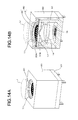
- FIG. 14A shows the outer appearance of a chassis in which the imaging optical system 2 is accommodated
- FIG. 14B is a cross-sectional view thereof.
- the optical system in the chassis is in the configuration of the third embodiment described by referring to FIGS. 7A and 7B .
- the chassis as a whole is a combination of a chassis body 60 and a base 61 .
- the first lens 11 As shown in FIG. 14B , on the chassis body 60 side in the chassis, incorporated are the first lens 11 , and the aperture/slit plate 40 (the aperture stops 13 and the fixed slit plate 20 ). On the base 61 side therein, the second and third lenses 12 and 14 are retained, and the image sensor 16 is disposed.
- the moving slit plates 30 A and 30 B are also provided at the aperture stop position, i.e., to be adjacent to the aperture/slit plate 40 .
- the chassis is made of metal such as aluminum or resin, and using a conductive material such as conductive metal or conductive resin is appropriate.
- a conductive material such as conductive metal or conductive resin
- chassis is desirably hermetically sealed not to attract dust and dirt that may cause malfunction of the moving slit plate 30 .
- FIGS. 15A and 15B The actuator 8 is disposed as shown in FIGS. 15A and 15B .
- FIG. 15A shows actuators 8 A and 8 B disposed on the base 61 .
- the actuators 8 A and 8 B are those using the bimorph piezo elements 50 described by referring to FIG. 11 .
- FIG. 15B shows only the actuators 8 A and 8 B, and the moving slit plates 30 A and 30 B.
- the moving slit plate 30 A is retained by the actuators 8 A. That is, the upper right and lower left end portions of the moving slit plate 30 A in the drawing are connected to junction sections 55 A (slit plate retention sections) of a pair of bimorph piezo elements 50 A in the actuators 8 A.
- the moving slit plate 30 B is retained by the actuators 8 B. That is, upper left and lower right end portions of the moving slit plate 30 B in the drawing are connected to junction sections 55 B (slit plate retention sections) of a pair of bimorph piezo elements 50 B in the actuators 8 B.
- the two actuators 8 A and 8 B are so disposed that their bimorph piezo elements 50 , i.e., the portions of the center electrodes 51 in FIG. 11 , are alternately provided.
- the actuators 8 A and 8 B are so disposed that a line segment connecting the junction sections 55 A of the actuator 8 A in charge of driving the moving slit plate 30 A, i.e., alternate long and short dashed lines a-a in FIG. 15B , is roughly orthogonal to a line segment connecting the junction sections 55 B of the actuator 8 B in charge of driving the remaining moving slit plate 30 B, i.e., alternate long and short dashed lines b-b in FIG. 15B .
- the actuators 8 A and 8 B By disposing the actuators 8 A and 8 B to have the alternate long and short dashed lines a-a and b-b being orthogonal to each other, the actuators 8 A and 8 B occupy a smaller space in the chassis. Moreover, with the configuration in which the moving slit plates 30 A and 30 B are respectively retained by the actuators 8 A and 8 B at their two diagonally-opposite portions, the moving slit plates 30 A and 30 B are retained and moved with stability, and what is more, the actuators 8 A and 8 B are not disposed one on the other.
- FIGS. 15A and 15B the layout of the actuators as shown in FIGS. 15A and 15B is suitable when a plurality of moving slit plates 30 are in use. Therefore, such an actuator layout is suitable not only in the case of FIGS. 7A and 7B but also in the case of FIGS. 6A and 6B or 9 A and 9 B, i.e., suitable for the actuators 8 A and 8 B with the two moving slit plates 30 A and 30 B.
- the actuator layout is also applicable to a case with a larger number of the moving slit plates 30 as shown in FIGS. 8A and 8B .
- the actuators 8 A and 8 B for the moving slit plates 30 A and 30 B in FIGS. 8A and 8B may be laid out as shown in FIGS. 15A and 15B
- the actuators for the moving slit plate 30 C may be so laid out that the two bimorph piezo elements are provided next to the actuator 8 A, for example.
- the slits may be formed differently, i.e., the shape and layout pattern of the transmission sections 22 and 32 , and those of the block sections 23 and 33 .
- the moving slit plate 30 described above is formed with the linear slits (precisely, the transmission sections 32 are rectangular), but the slits may be curved, bent, or crimped, for example. Still alternatively, the transmission sections 32 may be in a staggered arrangement to be in a checkered arrangement with the block sections 33 .
- the configuration of the transmission/block section SH is not restrictive as long as it includes a plurality of slit plates, and creates the states of transmission and blocking by the partial or entire movement of the slit plates.
- exemplified in the second to fourth embodiments is the case that a plurality of moving slit plates 30 are driven in the opposite directions. Alternatively, all of the moving slit plates 30 may be driven in the same direction.
- the optical system includes three lenses.
- the present disclosure is applicable also to an imaging optical system including four or more lenses, or two or less lenses, for example.
- the present disclosure is also in the following structures.
- An imaging apparatus including:
- an imaging element section configured to include a plurality of pixels
- an imaging optical system configured to form an image on the imaging element section, the image being formed by an electromagnetic wave from an outside;
- a transmission/block section configured to transmit and block the electromagnetic wave to/against the imaging element section, the transmission/block section being disposed at an aperture stop position in the imaging optical system;
- an actuator configured to drive the transmission/block section to move back and forth to be changed in state between transmission and blocking
- an output section configured to produce an image signal output, the image signal output being differential signaling between a pixel output from the imaging element section when the transmission/block section is in the state of transmission, and a pixel output from the imaging element section when the transmission/block section is in the state of blocking.
- the transmission/block section is formed to include a plurality of slit plates.
- the transmission/block section is formed to include a fixed slit plate and a moving slit plate, the moving slit plate being driven by the actuator to move back and forth.
- the moving slit plate includes a plurality of moving slit plates.
- the moving slit plate includes a plurality of moving slit plates, the plurality of moving slit plates being driven to move back and forth in opposite directions.
- the fixed slit plate is configured to serve also as an aperture stop in the imaging optical system.
- the plurality of slit plates in the transmission/block section are all moving slit plates, the moving slit plates being driven by the actuator to move back and forth.
- the actuator is any of a Lorentz force actuator, polymer actuator, an electromagnet actuator, and a piezo actuator.
- the actuator is a piezo actuator using a bimorph piezo element
- the bimorph piezo element is formed to include
- the transmission/block section includes a plurality of moving slit plates, the moving slit plates being driven by the actuator to move back and forth, the actuator includes a first actuator and a second actuator, and
- the first actuator and the second actuator are disposed to obtain an almost orthogonal relationship between a first line segment and a second line segment, the first line segment connecting a pair of slit plate retention sections in the first actuator in charge of driving one of the plurality of moving slit plates, the second line segment connecting a pair of slit plate retention sections in the second actuator in charge of driving another one of the plurality of moving slit plates.
- the imaging optical system, the imaging element section, and the transmission/block section are provided in a chassis, the chassis being made of a conductive material and being grounded.
- the conductive material is a conductive resin.
- the imaging optical system, the imaging element section, and the transmission/block section are hermetically sealed in the chassis.
Abstract
Description
-
- 1-1 Configuration of Imaging Optical System
- 1-2 Configuration of Imaging Apparatus
-
- a center electrode connected to the transmission/block section, the center electrode being grounded,
- a piezoelectric element provided on both surface sides of the center electrode,
- two surface electrodes each provided on a surface of the piezoelectric element, the surface not being on a side of the center electrode, the surface electrodes being short circuited to each other, and the surface electrodes being provided with an alternating drive voltage, and
- a conductive plate disposed to be insulated to each of the two surface electrodes, the conductive plate being grounded.
Claims (17)
Applications Claiming Priority (2)
| Application Number | Priority Date | Filing Date | Title |
|---|---|---|---|
| JP2011-233687 | 2011-10-25 | ||
| JP2011233687A JP2013093692A (en) | 2011-10-25 | 2011-10-25 | Imaging apparatus and imaging method |
Publications (2)
| Publication Number | Publication Date |
|---|---|
| US20130099097A1 US20130099097A1 (en) | 2013-04-25 |
| US9140895B2 true US9140895B2 (en) | 2015-09-22 |
Family
ID=48135210
Family Applications (1)
| Application Number | Title | Priority Date | Filing Date |
|---|---|---|---|
| US13/655,145 Expired - Fee Related US9140895B2 (en) | 2011-10-25 | 2012-10-18 | Imaging apparatus and imaging method for obtaining images fro electromagnetic waves |
Country Status (3)
| Country | Link |
|---|---|
| US (1) | US9140895B2 (en) |
| JP (1) | JP2013093692A (en) |
| CN (1) | CN103076100A (en) |
Families Citing this family (3)
| Publication number | Priority date | Publication date | Assignee | Title |
|---|---|---|---|---|
| US10270947B2 (en) * | 2016-09-15 | 2019-04-23 | Microsoft Technology Licensing, Llc | Flat digital image sensor |
| WO2019033349A1 (en) * | 2017-08-17 | 2019-02-21 | 深圳信炜科技有限公司 | Anti-aliasing imaging element, photosensitive module, display module and electronic device |
| US10571260B2 (en) * | 2017-09-06 | 2020-02-25 | The Boeing Company | Automated rivet measurement system |
Citations (8)
| Publication number | Priority date | Publication date | Assignee | Title |
|---|---|---|---|---|
| US4774564A (en) * | 1986-09-09 | 1988-09-27 | Fuji Photo Film Co., Ltd. | Electronic still camera for compensating color temperature dependency of color video signals |
| US20010041843A1 (en) * | 1999-02-02 | 2001-11-15 | Mark Modell | Spectral volume microprobe arrays |
| US6813046B1 (en) * | 2000-11-07 | 2004-11-02 | Eastman Kodak Company | Method and apparatus for exposure control for a sparsely sampled extended dynamic range image sensing device |
| JP2004317152A (en) | 2003-04-11 | 2004-11-11 | Mitsubishi Electric Corp | Thermal type infrared detector and infrared focal plane array |
| US20060127085A1 (en) * | 2003-08-21 | 2006-06-15 | Kaoru Matsuki | Electrostatic actuator, shutter device, imaging module, and camera |
| US20100061715A1 (en) * | 2008-09-11 | 2010-03-11 | Panasonic Corporation | Camera system and camera body |
| US20110176799A1 (en) * | 2010-01-15 | 2011-07-21 | Panasonic Corporation | Focal plane shutter device and imaging device |
| US20120194718A1 (en) * | 2011-02-01 | 2012-08-02 | Kabushiki Kaisha Toshiba | Solid state imaging device |
-
2011
- 2011-10-25 JP JP2011233687A patent/JP2013093692A/en active Pending
-
2012
- 2012-10-18 CN CN2012103981645A patent/CN103076100A/en active Pending
- 2012-10-18 US US13/655,145 patent/US9140895B2/en not_active Expired - Fee Related
Patent Citations (9)
| Publication number | Priority date | Publication date | Assignee | Title |
|---|---|---|---|---|
| US4774564A (en) * | 1986-09-09 | 1988-09-27 | Fuji Photo Film Co., Ltd. | Electronic still camera for compensating color temperature dependency of color video signals |
| US20010041843A1 (en) * | 1999-02-02 | 2001-11-15 | Mark Modell | Spectral volume microprobe arrays |
| US6813046B1 (en) * | 2000-11-07 | 2004-11-02 | Eastman Kodak Company | Method and apparatus for exposure control for a sparsely sampled extended dynamic range image sensing device |
| JP2004317152A (en) | 2003-04-11 | 2004-11-11 | Mitsubishi Electric Corp | Thermal type infrared detector and infrared focal plane array |
| US7005644B2 (en) | 2003-04-11 | 2006-02-28 | Mitsubishi Denki Kabushiki Kaisha | Thermal infrared detector and infrared focal plane array |
| US20060127085A1 (en) * | 2003-08-21 | 2006-06-15 | Kaoru Matsuki | Electrostatic actuator, shutter device, imaging module, and camera |
| US20100061715A1 (en) * | 2008-09-11 | 2010-03-11 | Panasonic Corporation | Camera system and camera body |
| US20110176799A1 (en) * | 2010-01-15 | 2011-07-21 | Panasonic Corporation | Focal plane shutter device and imaging device |
| US20120194718A1 (en) * | 2011-02-01 | 2012-08-02 | Kabushiki Kaisha Toshiba | Solid state imaging device |
Also Published As
| Publication number | Publication date |
|---|---|
| JP2013093692A (en) | 2013-05-16 |
| CN103076100A (en) | 2013-05-01 |
| US20130099097A1 (en) | 2013-04-25 |
Similar Documents
| Publication | Publication Date | Title |
|---|---|---|
| US11287515B2 (en) | Rotating compact light ranging system comprising a stator driver circuit imparting an electromagnetic force on a rotor assembly | |
| US8803976B2 (en) | Image pickup apparatus | |
| US8786861B2 (en) | Optical device with variable wavelength interference filter | |
| US10764484B2 (en) | Imaging system | |
| EP2870507B1 (en) | Camera module | |
| TWI567370B (en) | Pyroelectric infrared radiation sensor | |
| US9140895B2 (en) | Imaging apparatus and imaging method for obtaining images fro electromagnetic waves | |
| JP6081830B2 (en) | Position detection device using a reflective photosensor | |
| JP5325312B2 (en) | Viewing angle limiting cover and infrared sensor provided with the same | |
| CN112946857B (en) | Infrared detector module with automatic focusing and resetting correction functions | |
| US11082663B2 (en) | Imaging system | |
| JP2002064195A (en) | Photoelectric conversion element and photosensor array | |
| JP6601761B2 (en) | Infrared detector | |
| CN211406089U (en) | Imaging device and electronic apparatus | |
| WO2017163760A1 (en) | Infrared detection device | |
| US20170269235A1 (en) | Radiation detection apparatus and radiation imaging system | |
| CN112929536A (en) | Camera module, electronic equipment and vehicle | |
| JP2014191032A (en) | Camera module and portable terminal | |
| WO2019039498A1 (en) | Infrared detection device | |
| CN113132582A (en) | Imaging method, imaging device and electronic equipment |
Legal Events
| Date | Code | Title | Description |
|---|---|---|---|
| AS | Assignment |
Owner name: SONY CORPORATION, JAPAN Free format text: ASSIGNMENT OF ASSIGNORS INTEREST;ASSIGNORS:ISOBE, HIROSHI;KABASAWA, HIDETOSHI;SAITO, MASAHIRO;AND OTHERS;SIGNING DATES FROM 20121115 TO 20121129;REEL/FRAME:029420/0879 |
|
| STCF | Information on status: patent grant |
Free format text: PATENTED CASE |
|
| FEPP | Fee payment procedure |
Free format text: PAYOR NUMBER ASSIGNED (ORIGINAL EVENT CODE: ASPN); ENTITY STATUS OF PATENT OWNER: LARGE ENTITY |
|
| MAFP | Maintenance fee payment |
Free format text: PAYMENT OF MAINTENANCE FEE, 4TH YEAR, LARGE ENTITY (ORIGINAL EVENT CODE: M1551); ENTITY STATUS OF PATENT OWNER: LARGE ENTITY Year of fee payment: 4 |
|
| FEPP | Fee payment procedure |
Free format text: MAINTENANCE FEE REMINDER MAILED (ORIGINAL EVENT CODE: REM.); ENTITY STATUS OF PATENT OWNER: LARGE ENTITY |
|
| LAPS | Lapse for failure to pay maintenance fees |
Free format text: PATENT EXPIRED FOR FAILURE TO PAY MAINTENANCE FEES (ORIGINAL EVENT CODE: EXP.); ENTITY STATUS OF PATENT OWNER: LARGE ENTITY |
|
| STCH | Information on status: patent discontinuation |
Free format text: PATENT EXPIRED DUE TO NONPAYMENT OF MAINTENANCE FEES UNDER 37 CFR 1.362 |
|
| FP | Lapsed due to failure to pay maintenance fee |
Effective date: 20230922 |