US8770761B2 - Illumination unit, projection display unit, and direct view display unit - Google Patents
Illumination unit, projection display unit, and direct view display unit Download PDFInfo
- Publication number
- US8770761B2 US8770761B2 US13/276,818 US201113276818A US8770761B2 US 8770761 B2 US8770761 B2 US 8770761B2 US 201113276818 A US201113276818 A US 201113276818A US 8770761 B2 US8770761 B2 US 8770761B2
- Authority
- US
- United States
- Prior art keywords
- light
- emitting
- solid
- light source
- chips
- Prior art date
- Legal status (The legal status is an assumption and is not a legal conclusion. Google has not performed a legal analysis and makes no representation as to the accuracy of the status listed.)
- Active, expires
Links
Images


Classifications
-
- F—MECHANICAL ENGINEERING; LIGHTING; HEATING; WEAPONS; BLASTING
- F21—LIGHTING
- F21V—FUNCTIONAL FEATURES OR DETAILS OF LIGHTING DEVICES OR SYSTEMS THEREOF; STRUCTURAL COMBINATIONS OF LIGHTING DEVICES WITH OTHER ARTICLES, NOT OTHERWISE PROVIDED FOR
- F21V5/00—Refractors for light sources
- F21V5/007—Array of lenses or refractors for a cluster of light sources, e.g. for arrangement of multiple light sources in one plane
-
- F—MECHANICAL ENGINEERING; LIGHTING; HEATING; WEAPONS; BLASTING
- F21—LIGHTING
- F21V—FUNCTIONAL FEATURES OR DETAILS OF LIGHTING DEVICES OR SYSTEMS THEREOF; STRUCTURAL COMBINATIONS OF LIGHTING DEVICES WITH OTHER ARTICLES, NOT OTHERWISE PROVIDED FOR
- F21V29/00—Protecting lighting devices from thermal damage; Cooling or heating arrangements specially adapted for lighting devices or systems
- F21V29/85—Protecting lighting devices from thermal damage; Cooling or heating arrangements specially adapted for lighting devices or systems characterised by the material
-
- F—MECHANICAL ENGINEERING; LIGHTING; HEATING; WEAPONS; BLASTING
- F21—LIGHTING
- F21V—FUNCTIONAL FEATURES OR DETAILS OF LIGHTING DEVICES OR SYSTEMS THEREOF; STRUCTURAL COMBINATIONS OF LIGHTING DEVICES WITH OTHER ARTICLES, NOT OTHERWISE PROVIDED FOR
- F21V5/00—Refractors for light sources
- F21V5/008—Combination of two or more successive refractors along an optical axis
-
- F—MECHANICAL ENGINEERING; LIGHTING; HEATING; WEAPONS; BLASTING
- F21—LIGHTING
- F21V—FUNCTIONAL FEATURES OR DETAILS OF LIGHTING DEVICES OR SYSTEMS THEREOF; STRUCTURAL COMBINATIONS OF LIGHTING DEVICES WITH OTHER ARTICLES, NOT OTHERWISE PROVIDED FOR
- F21V5/00—Refractors for light sources
- F21V5/04—Refractors for light sources of lens shape
- F21V5/045—Refractors for light sources of lens shape the lens having discontinuous faces, e.g. Fresnel lenses
-
- F—MECHANICAL ENGINEERING; LIGHTING; HEATING; WEAPONS; BLASTING
- F21—LIGHTING
- F21V—FUNCTIONAL FEATURES OR DETAILS OF LIGHTING DEVICES OR SYSTEMS THEREOF; STRUCTURAL COMBINATIONS OF LIGHTING DEVICES WITH OTHER ARTICLES, NOT OTHERWISE PROVIDED FOR
- F21V9/00—Elements for modifying spectral properties, polarisation or intensity of the light emitted, e.g. filters
- F21V9/08—Elements for modifying spectral properties, polarisation or intensity of the light emitted, e.g. filters for producing coloured light, e.g. monochromatic; for reducing intensity of light
-
- G—PHYSICS
- G03—PHOTOGRAPHY; CINEMATOGRAPHY; ANALOGOUS TECHNIQUES USING WAVES OTHER THAN OPTICAL WAVES; ELECTROGRAPHY; HOLOGRAPHY
- G03B—APPARATUS OR ARRANGEMENTS FOR TAKING PHOTOGRAPHS OR FOR PROJECTING OR VIEWING THEM; APPARATUS OR ARRANGEMENTS EMPLOYING ANALOGOUS TECHNIQUES USING WAVES OTHER THAN OPTICAL WAVES; ACCESSORIES THEREFOR
- G03B21/00—Projectors or projection-type viewers; Accessories therefor
- G03B21/005—Projectors using an electronic spatial light modulator but not peculiar thereto
-
- G—PHYSICS
- G03—PHOTOGRAPHY; CINEMATOGRAPHY; ANALOGOUS TECHNIQUES USING WAVES OTHER THAN OPTICAL WAVES; ELECTROGRAPHY; HOLOGRAPHY
- G03B—APPARATUS OR ARRANGEMENTS FOR TAKING PHOTOGRAPHS OR FOR PROJECTING OR VIEWING THEM; APPARATUS OR ARRANGEMENTS EMPLOYING ANALOGOUS TECHNIQUES USING WAVES OTHER THAN OPTICAL WAVES; ACCESSORIES THEREFOR
- G03B21/00—Projectors or projection-type viewers; Accessories therefor
- G03B21/14—Details
- G03B21/20—Lamp housings
- G03B21/2006—Lamp housings characterised by the light source
- G03B21/2013—Plural light sources
-
- G—PHYSICS
- G03—PHOTOGRAPHY; CINEMATOGRAPHY; ANALOGOUS TECHNIQUES USING WAVES OTHER THAN OPTICAL WAVES; ELECTROGRAPHY; HOLOGRAPHY
- G03B—APPARATUS OR ARRANGEMENTS FOR TAKING PHOTOGRAPHS OR FOR PROJECTING OR VIEWING THEM; APPARATUS OR ARRANGEMENTS EMPLOYING ANALOGOUS TECHNIQUES USING WAVES OTHER THAN OPTICAL WAVES; ACCESSORIES THEREFOR
- G03B21/00—Projectors or projection-type viewers; Accessories therefor
- G03B21/14—Details
- G03B21/20—Lamp housings
- G03B21/2006—Lamp housings characterised by the light source
- G03B21/2033—LED or laser light sources
-
- H—ELECTRICITY
- H04—ELECTRIC COMMUNICATION TECHNIQUE
- H04N—PICTORIAL COMMUNICATION, e.g. TELEVISION
- H04N9/00—Details of colour television systems
- H04N9/12—Picture reproducers
- H04N9/31—Projection devices for colour picture display, e.g. using electronic spatial light modulators [ESLM]
- H04N9/3138—Projection devices for colour picture display, e.g. using electronic spatial light modulators [ESLM] using arrays of modulated light sources
-
- H—ELECTRICITY
- H04—ELECTRIC COMMUNICATION TECHNIQUE
- H04N—PICTORIAL COMMUNICATION, e.g. TELEVISION
- H04N9/00—Details of colour television systems
- H04N9/12—Picture reproducers
- H04N9/31—Projection devices for colour picture display, e.g. using electronic spatial light modulators [ESLM]
- H04N9/3141—Constructional details thereof
- H04N9/315—Modulator illumination systems
- H04N9/3161—Modulator illumination systems using laser light sources
Definitions
- the present disclosure relates to an illumination unit using a solid-state light-emitting device including laser diodes (LDs).
- LDs laser diodes
- the present disclosure is directed to a projection display unit and a direct view display unit which both are equipped with the illumination unit.
- a typical projector which are configured to project images to a screen, are widely used in offices as well as households.
- a typical projector is designed to generate optical images by modulating light from a light source using a light bulb and to project the optical images to a screen. As a result, the images are displayed on a screen.
- tiny or palm-size projectors and portable phones equipped with such a tiny projector are commercially available (for example, refer to Japanese Unexamined patent Application Publication No. 2008-134324).
- a projector mainly uses a high-intensity discharge lamp as a light source.
- a lamp of this type is relatively large in size and has high power consumption. Therefore, attempts to replace a high-intensity discharge lamp with a solid-state light-emitting device, including light emitting diodes (LEDs), laser diodes (LDs), and organic light emitting devices (OLEDs), are currently attracting interest.
- Solid-state light-emitting devices are advantageous over high-intensity discharge lamps in terms of compactness, power consumption, and reliability.
- a projector as described above displays color images by using individual light beams of three primary colors, that is, red (R), green (G), and blue (B) light beams.
- R red
- G green
- B blue
- intensities or luminance properties may be different for the respective colors among devices (or chips in a solid-state light-emitting device) which emit the light beams of the three primary colors, respectively. In this case, it is difficult to increase the luminance of illumination light as a whole output from the illumination system.
- an illumination unit which makes it possible to increase luminance of illumination light. Also, it is desirable to provide a projection display unit and a direct view display unit which both are equipped with the illumination unit.
- An illumination unit includes: one or more light sources each including a solid-state light-emitting device configured to emit light from a light emission region including a single or a plurality of light-emitting spots, the solid-state light-emitting device including a single chip or a plurality of chips each emitting a light beam, wherein three or more of the light-emitting spots are provided within the whole of one or more light sources, to allow the whole of one or more light sources to emit light beams in two or more wavelength bands different from one another, and the solid-state light emitting device in a first light source which is at least one of the one or more light sources, has a plurality of light-emitting spots which emit light in the same wavelength band.
- a projection display unit includes: an illumination optical system; a spatial modulation device modulating light from the illumination optical system based on an input picture signal to generate imaging light; and a projection optical system projecting the imaging light generated by the spatial modulation device, the illumination optical system including one or more light sources each including a solid-state light-emitting device configured to emit light from a light emission region including a single or a plurality of light-emitting spots, the solid-state light-emitting device including a single chip or a plurality of chips each emitting a light beam, wherein three or more of the light-emitting spots are provided within the whole of one or more light sources, to allow the whole of one or more light sources to emit light beams in two or more wavelength bands different from one another, and the solid-state light emitting device in a first light source which is at least one of the one or more light sources, has a plurality of light-emitting spots which emit light in the same wavelength band.
- a direct view display unit includes: an illumination optical system; a spatial modulation device modulating light from the illumination optical system based on an input picture signal to generate imaging light; a projection optical system projecting the imaging light generated by the spatial modulation device; and a transmissive screen displaying the imaging light projected from the projection optical system
- the illumination optical system including one or more light sources each including a solid-state light-emitting device configured to emit light from a light emission region including a single or a plurality of light-emitting spots, the solid-state light-emitting device including a single chip or a plurality of chips each emitting a light beam, wherein three or more of the light-emitting spots are provided within the whole of one or more light sources, to allow the whole of one or more light sources to emit light beams in two or more wavelength bands different from one another, and the solid-state light emitting device in a first light source which is at least one of the one or more light sources, has a plurality of light-emitting spots which emit
- the three or more of the light-emitting spots are provided within the whole of one or more light sources, to allow the whole of one or more light sources to emit the light beams in the two or more wavelength bands different from one another, and the solid-state light emitting device in at least one of the one or more light sources (for example, the first light source), has the plurality of light-emitting spots which emit the light in the same wavelength band.
- the illumination unit emits the light beams in two or more wavelength bands as illumination light.
- the illumination unit, the projection display unit, and the direct view display unit each further include one or more traveling-direction angle conversion device each converting a traveling-direction-angle of the light entering from the solid-state light-emitting device; and an integrator uniformalizing illumination distribution in a predetermined illumination region which is to be illuminated by light from the traveling-direction angle conversion device.
- the integrator includes a first fly-eye lens having cells which receive light from the traveling-direction angle conversion device, and a second fly-eye lens having cells which receive light from the first fly-eye lens, and an optical system configured with the traveling-direction angle conversion device and the first and second fly-eye lenses has an optical magnification which allows each of light source images to have a size not exceeding a size of the cell in the second fly-eye lens, the light source images being formed on the second fly-eye lens by the respective cells in the first fly-eye lens.
- the light incident on the second fly-eye lens reaches the illumination region efficiently. Thus, it is unlikely that one light source image is formed across a plurality of cells, making it possible to improve light use efficiency of the illumination unit.
- the three or more of the light-emitting spots are provided within the whole of one or more light sources, to allow the whole of one or more light sources to emit the light beams in the two or more wavelength bands different from one another, and the solid-state light emitting device in the first light source which is at least one of the one or more light sources, has the plurality of light-emitting spots which emit the light in the same wavelength band. This makes it possible to adjust relative light emission intensities between the light of the respective wavelength bands when the illumination unit emits the light beams in two or more wavelength bands as illumination light, and to increase the luminance of the illumination light.
- the plurality of light-emitting spots which emit the light in the same wavelength band are provided in at least one of the one or more light sources (for example, the first light source). This makes it possible to eliminate any optical unification or unifying members for unifying the light beams emitted from those light-emitting spots. It is thus possible to achieve compactness of the units, or to prevent the units from being enlarged as well.
- FIG. 1A shows a schematic structure of a projector according to a first embodiment of the technology as seen from the above.
- FIG. 1B shows the schematic structure of the projector as seen from one side.
- FIG. 2A shows exemplary optical paths in the projector of FIGS. 1A and 1B as seen from the above.
- FIG. 2B shows the optical paths in the projector of FIGS. 1A and 1B as seen from the side.
- FIG. 3A shows a top view of an exemplary structure of the light source, when a light source in the projector of FIGS. 1A and 1B has a chip of an upper surface emitting type.
- FIG. 3B shows a cross-section of the structure of the light source, taken along the line A-A of FIG. 3A .
- FIG. 4A shows a top view of another exemplary structure of the light source, when a light source in the projector of FIGS. 1A and 1B has a chip of an upper surface emitting type.
- FIG. 4B shows a cross-section of the structure of the light source, taken along the line A-A of FIG. 4A .
- FIG. 5A shows a top view of still another exemplary structure of the light source, when a light source in the projector of FIGS. 1A and 1B has a chip of an upper surface emitting type.
- FIG. 5B shows a cross-section of the structure of the light source, taken along the line A-A of FIG. 5A .
- FIG. 6A shows a top view of an exemplary arrangement of a light-emitting spot on the light source, when a chip in a light source in the projector of FIGS. 1A and 1B has an upper surface emitting type.
- FIG. 6B shows a top view of another exemplary arrangement of a light-emitting spot on the light source, when a chip in a light source in the projector of FIGS. 1A and 1B has an upper surface emitting type.
- FIG. 6C shows a top view of still another exemplary arrangement of a light-emitting spot on the light source, when a chip in a light source in the projector of FIGS. 1A and 1B has an upper surface emitting type.
- FIG. 7A shows a cross section of an exemplary structure of a light source in the projector of FIGS. 1A and 1B , when chips in the light source are of a side surface emitting type.
- FIG. 7B shows a solid-state light-emitting device in the light source as seen from its light emitting surface.
- FIG. 8A shows a cross section of another exemplary structure of a light source in the projector of FIGS. 1A and 1B , when chips in the light source are of a side surface emitting type.
- FIG. 8B shows a solid-state light-emitting device in the light source as seen from its light emitting surface.
- FIG. 9A shows a cross section of further another exemplary structure of a light source in the projector of FIGS. 1A and 1B , when chips in the light source are of a side surface emitting type.
- FIG. 9B shows a solid-state light-emitting device in the light source as seen from its light emitting surface.
- FIG. 9C shows a solid-state light-emitting device of a monolithic structure in the light source as seen from its light emitting surface.
- FIG. 10A shows a cross section of the structure of the light source of FIG. 7A , when it is angled 90 degrees on the XY plane.
- FIG. 10B shows the solid-state light-emitting device in the light source as seen from its light emitting surface.
- FIG. 11A shows a cross section of the structure of the light source of FIG. 8A , when it is angled 90 degrees on the XY plane.
- FIG. 11B shows the solid-state light-emitting device in the light source as seen from its light emitting surface.
- FIG. 12A shows a cross section of the structure of the light source of FIGS. 9A to 9C , when it is angled 90 degrees on the XY plane.
- FIG. 12B shows the solid-state light-emitting device in the light source as seen from its light emitting surface.
- FIG. 12C shows a solid-state light-emitting device of a monolithic structure in the light source as seen from its light emitting surface.
- FIG. 13A shows a schematic structure of a pre-fly-eye lens.
- FIG. 13B shows a schematic structure of a post-fly-eye lens.
- FIG. 14A schematically shows an exemplary arrangement of light-emitting spots formed on individual light sources in the projector of FIGS. 1A and 1B .
- FIG. 14B schematically shows another exemplary arrangement of light-emitting spots formed on individual light sources in the projector of FIGS. 1A and 1B .
- FIG. 14C schematically shows still another exemplary arrangement of light-emitting spots formed on individual light sources in the projector of FIGS. 1A and 1B .
- FIG. 15A shows an exemplary relationship of an arrangement and FFPs of light-emitting spots formed on a light source in the projector of FIGS. 1A and 1B .
- FIG. 15B shows another exemplary relationship of an arrangement and FFPS of light-emitting spots formed on a light source in the projector of FIGS. 1A and 1B .
- FIG. 16 schematically shows exemplary light source images on the cells of the post-fly-eye lens in the projector of FIGS. 1A and 1B .
- FIG. 17 schematically shows a size of an illumination region on a spatial modulation device in the projector of FIGS. 1A and 1B .
- FIG. 18A shows a schematic structure of a projector according to a second embodiment of the technology as seen from the above.
- FIG. 18B shows the schematic structure of the projector as seen from one side.
- FIG. 19A shows a schematic structure of a projector according to a third embodiment of the technology as seen from the above.
- FIG. 19B shows the schematic structure of the projector as seen from one side.
- FIG. 20A shows exemplary optical paths in the projector of FIGS. 19A and 19B as seen from the above.
- FIG. 20B shows the optical paths in the projector of FIGS. 19A and 19B as seen from the side.
- FIG. 21 schematically shows an exemplary arrangement of light-emitting spots formed on a light source in the projector of FIGS. 1A and 1B .
- FIG. 22A schematically shows an exemplary arrangement of light-emitting spots formed on individual light sources in the projector of modification 1.
- FIG. 22B schematically shows another exemplary arrangement of light-emitting spots formed on individual light sources in the projector of the modification 1.
- FIG. 22C schematically shows still another exemplary arrangement of light-emitting spots formed on individual light sources in the projector of the modification 1.
- FIG. 23 shows a cross section of an exemplary structure of a light source in the projector of modification 2.
- FIG. 24 shows an exemplary relationship of an arrangement and FFPs of light-emitting spots formed on a light source in the projector of FIG. 23 .
- FIG. 25A shows a schematic structure of a projector of modification 3 as seen from the above.
- FIG. 25B shows the schematic structure of the projector of the modification 3 as seen from one side.
- FIG. 26 shows a schematic structure of a rear projection display device equipped of the illumination optical system according to any one of the embodiments and the modifications.
- Second embodiment (an example of using a reflective device as a spatial modulation device)
- Modification 1 (another example of using multiple light sources provided in an illumination optical system)
- Modification 2 (an example of using chips arranged at angles with respect to a light axis in a light source)
- Modification 3 (an example of eliminating an integrator and a condenser lens from an illumination optical system)
- FIGS. 1A and 1B show a schematic structure of a projector according to a first embodiment of the technology (called a “projector 1 ” herein). Note that this projector 1 corresponds to a concrete example of a “projection display unit” according to one embodiment of the technology.
- FIG. 1A shows the structure of the projector 1 as seen from the above or on a Y axis, and FIG. 1B shows the same as seen from one side or on an X axis.
- FIGS. 2A and 2B show optical paths in the projector 1 of FIGS. 1A and 1B .
- FIG. 2A shows the optical paths as seen from the above or on the Y axis, and FIG. 2B shows those optical paths as seen from the side or on an X axis.
- the Y axis extends vertically and the X axis extends horizontally, but this embodiment is not limited to this orientation.
- the Y axis may extend horizontally and the X axis may extend vertically.
- an explanation will be given based on the premise that the Y and X axes are vertical and horizontal axes, respectively in the embodiments.
- a “horizontal direction” indicates a direction on the X axis
- a “vertical direction” indicates a direction on the Y axis.
- the projector 1 includes, but not limited to, an illumination optical system 1 A, a spatial modulation device 60 , and a projection optical system 70 .
- the spatial modulation device 60 generates optical images (imaging light) by modulating, based on input picture signals, light beams from the illumination optical system 1 A, and the projection optical system 70 projects the optical images from the spatial modulation device 60 to a reflection screen 2 .
- the illumination optical system 1 A corresponds to a concrete example of an “illumination unit” according to one embodiment of the technology.
- the illumination optical system 1 A has a function of delivering light beams for irradiating an illumination region 60 A on the spatial modulation device 60 .
- any optical device may be located within a region in which the light beams travel, as necessary.
- An example of the optical device is an optical filter for attenuating light other than the visible light of light output from the illumination optical system 1 A.
- the illumination optical system 1 A includes, but not limited to, light sources 10 A, 10 B, and 10 C, coupling lens (or traveling-direction angle conversion devices) 20 A, 20 B, and 20 C, an optical path unifying device 30 , an integrator 40 , and a condenser lens 50 .
- the optical path unifying device 30 has a function of unifying the respective light beams from the light sources 10 A, 10 B, and 10 C.
- This optical path unifying device 30 includes, but not limited to, two dichroic mirrors 30 A and 30 B.
- the integrator 40 has a function of allowing the illumination distribution of the light on the illumination region 60 A to be uniform, and it includes, but not limited to, a pair of fly-eye lenses 40 A and 40 B.
- the coupling lens 20 A, the optical path unifying device 30 , the integrator 40 , and the condenser lens 50 are aligned in this order from the location of the light source 10 A.
- the optical axis of the light source 10 B is perpendicular to that of the light source 10 A, and both axes intersects in the dichroic mirror 30 A.
- the coupling lens 20 B and the dichroic mirror 30 A are aligned in this order from the location of the light source 10 B.
- the optical axis of the light source 10 C is also perpendicular to that of the light source 10 A, and both axes intersect in the dichroic mirror 30 B.
- the coupling lens 20 C and the dichroic mirror 30 B are aligned in this order from the location of the light source 10 C.
- the combination of the coupling lens (or traveling-direction angle conversion devices) 20 A, 20 B, and 20 C and the integrator 40 correspond to a concrete example of an optical member according to one embodiment of the technology.
- This optical member has a function of receiving light beams from solid-state light-emitting devices (described later) and allowing the light beams to pass through.
- the components other than the light sources 10 B and 10 C and the coupling lenses 20 B and 20 C are aligned with a line parallel to the Z axis.
- this embodiment is not limited to this alignment.
- these components (or a part thereof) may be arranged in a line which is not parallel to the Z axis.
- the layout of all the components in the illumination optical system 1 A may be rotated 90 degrees with respect to that of FIGS. 1A and 1B , so that the optical axis of the illumination optical system 1 A is perpendicular to the Z axis.
- an additional optical device such as a mirror is necessary in order to lead the light beams from the illumination optical system 1 A to the spatial modulation device 60 .
- the layout of the light source 10 A, the coupling lens 20 A, and the optical path unifying device 30 may be angled 90 degrees with respect to that of FIGS. 1A and 1B , so that their optical axis is perpendicular to the Z axis. Even in this case, an additional optical device such as a mirror is also necessary in order to lead the light beams from the optical path unifying device 30 to the integrator 40 .
- each of the light sources 10 A, 10 B, and 10 C includes, but not limited to, a solid-state light-emitting device 11 , and a package 12 in which the solid-state light-emitting device 11 is supported on a substrate material.
- each of the light sources 10 A, 10 B, and 10 C may be implemented by a package in which the solid-state light-emitting device 11 is supported on a substrate material.
- the solid-state light-emitting device 11 has a function of emitting light beams from a light emission region, and this light emission region has one or more light-emitting spots of a dot or non-dot shape.
- the solid-state light-emitting device 11 may be composed of the single chip 11 A which emits a light beam of a predetermined wavelength (wavelength band), as shown in exemplary FIGS. 3A and 3B .
- the device 11 may be composed of the multiple chips 11 A which emit light beams of the same wavelength or different wavelengths, as shown in exemplary FIG. 4A , 4 B, 5 A and 5 B.
- the chips 11 A may be arranged laterally in a line as shown in FIGS. 4A and 4B or may be arranged in a matrix form as shown in FIGS. 5A and 5B .
- the light sources 10 A, 10 B, and 10 C may have a different number of chips 11 or the same number of chips 11 in the respective solid-state light-emitting devices 11 .
- the size (W V ⁇ W H ) of the device 11 may be the same as the size (W V1 ⁇ W H1 ) of the single chip 11 A, as shown in FIG. 3A .
- the size of the device 11 may be the same as that of an area defined by arranging all the chips 11 A adjacent to one another, as shown in FIGS. 4A and 5A .
- the size (W V ⁇ W H ) of the device 11 is equal to the size (W V1 ⁇ 2W H1 ). Meanwhile, when the multiple chips 11 A are arranged in a matrix form as shown in FIG. 5A , the size (W V ⁇ W H ) of the device 11 is equal to the size (2W V1 ⁇ 2W H1 ).
- the chip 11 A may be any of a light-emitting diode (LED), an organic light-emitting device (OLED), and a laser diode (LD). All the chips 11 A in the light sources 10 A, 10 B, and 10 C may be any of LEDs, OLEDs or LDs. Alternatively, the chip 11 A in at least one of the light sources 10 A, 10 B, and 10 C may be an LED, and the chips 11 A in the others may be OLEDs. Furthermore, the chip 11 A in at least one of the light sources 10 A, 10 B, and 10 C may be an LED, and the chips 11 A in the others may be LDs.
- LED light-emitting diode
- OLED organic light-emitting device
- LD laser diode
- the chip 11 A in at least one of the light sources 10 A, 10 B, and 10 C may be an OLED, and the chips 11 A in the others may be LDs. However, it is preferable that all the chips 11 A in the light sources 10 A, 10 B, and 10 C include at least one LD.
- the respective chips 11 A in the light sources 10 A, 10 B, and 10 C may be designed to emit light beams of different wavelengths.
- the chip 11 A of the light source 10 A emits a light beam having a wavelength of about 400 nm to 500 nm or a blue light beam.
- the chip 11 A of the light source 10 B emits a light beam having a wavelength of about 500 nm to 600 nm or a green light beam.
- the chip 11 A of the light source 10 C emits a light beam having a wavelength of about 600 nm to 700 nm or a red light beam.
- the chip 11 A of the light source 10 A emits a light beam other than a blue light beam, that is, a green or red light beam.
- the chip 11 A of the light source 10 B emits a light beam other than a green light beam, that is, a blue or red light beam.
- the chip 11 A of the light source 10 C emits a light beam other than a red light beam, that is, a green or blue light beam. Concrete examples will be given later of colors of light beams from the chips 11 A in the light sources 10 A, 10 B, and 10 C with reference to exemplary FIGS. 14A to 14C .
- each chip 11 A has a light-emitting spot 11 B, of which size (P V1 ⁇ P H1 ) is smaller than the size (W V ⁇ W H ) of the chip 11 A itself.
- This light-emitting spot 11 B corresponds to a light emission region, that is, a region from which a light beam is emitted while the chip 11 A is driven by supplying a current thereto.
- the chip 11 A is an LED or OLED
- the light-emitting spot 11 B thereon has a non-dot shape, that is, a square or rectangular shape.
- the light-emitting spot 11 B thereon has a dot shape, and this spot is smaller than the light-emitting spot 11 B when the chip 11 A is an LED or OLED.
- the number of light-emitting spots 11 B formed thereon is one, as shown in exemplary FIG. 6A .
- the number of spots 11 B is plural, as described in detail later.
- the solid-state light-emitting device 11 is composed of the multiple chips 11 A, the light-emitting spot 11 B formed thereon are equal in number to the chips 11 A, as shown in exemplary FIGS. 6B and 6C .
- the number of spots 11 B is greater than that of the chips 11 A.
- the size (P V ⁇ P H ) of the light emission region in the device 11 is equal to the size (P V1 ⁇ P H1 ) of the light-emitting spot 11 B, as shown in FIG. 6A .
- the solid-state light-emitting device 11 has a monolithic structure as described above is made an exception.
- the size (P V ⁇ P H ) of the light emission region in the device 11 is equal to the size of the region defined by the outer frame of the light-emitting spots 11 B of the chips 11 A when all the chips 11 A are tiled with a minimum area.
- the size (P V ⁇ P H ) of the light emission region is larger than the size (P V1 ⁇ 2P H1 ) and smaller than the size (W V ⁇ W H ).
- the size (P V ⁇ P H ) of the light emission region is larger than the size (2P V1 ⁇ 2P H1 ) and smaller than the size (W V ⁇ W H ).
- the description has been given by exemplifying the case where the chips 11 A are of an upper surface emitting type.
- the chip 11 A may be of a side surface emitting type.
- a description will be give by exemplifying a case where the chips 11 A are of a side surface emitting type.
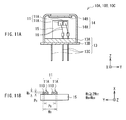
- each of the light sources 10 A, 10 B, and 10 C has a can type, and includes a stem 13 , a cap 14 , and the solid-state light-emitting device 11 composed of one or more side surface emitting type chips 11 A.
- the device 11 is placed within an inner space defined by the stem 13 and the cap 14 .
- each of the light sources 10 A, 10 B, and 10 C is implemented by a package that houses the solid-state light-emitting device 11 .
- the stem 13 and the cap 14 constitute the package in which the light sources 10 A, 10 B, 10 C, or 10 D (described later) is contained.
- This stem 13 includes, but not limited to, a support substrate 13 A supporting a sub-mount 15 , an outer-rim substrate 13 B located on the rear surface of the support substrate 13 A, and multiple connecting pins 13 C.
- the sub-mount 15 is made of conductive and heat dissipating material.
- Each of the support substrate 13 A and the outer-rim substrate 13 B is fabricated by forming one or more insulating through-holes and one or more conductive through-holes in a conductive and heat dissipating substrate.
- Each of the support substrate 13 A and the outer-rim substrate 13 B has, for example, a disc-shape, and both of them are stacked while being concentric with each other.
- the diameter of the outer-rim substrate 13 B is larger than that of the support substrate 13 A.
- the outer-rim substrate 13 B is a circular flange provided on a plane perpendicular to a central axis of the substrate 13 B, and is formed spreading out in the circumferential directions from the central axis. This circular flange serves as defining the reference position of the cap 14 with respect to the support substrate 13 A when the cap 14 is attached to the support substrate 13 during a fabrication process.
- the connecting pins 13 C pass through the support substrate 13 A and the like. All the connecting pins 13 C except at least one connecting pin, which are called “connecting pins ⁇ ” for convenience' sake, are electrically connected to the corresponding electrodes (not shown) on the chips 11 A, respectively.
- the connecting pins ⁇ extend both from the outer-rim substrate 13 B and from the support substrate 13 A.
- the portion of each connecting pin ⁇ which protrudes from the support substrate 13 A may be longer than that protruding from the outer-rim substrate 13 B.
- the connecting pin 13 C except the connecting pin ⁇ which is called a “connecting pin ⁇ ” for convenience' sake, is electrically connected to the other electrodes (not shown) on the chips 11 A.
- one end of the connecting pin ⁇ may protrude from the outer-rim substrate 13 B lengthwise, and the other end is embedded in the support substrate 13 A.
- the end of the connecting pin 13 C which protrudes far from the outer-rim substrate 13 B is to be inserted into, for example, a circuit board (not shown).
- the ends of the connecting pins 13 C which protrude a little from the support substrate 13 A are connected to the chips 11 A through wires 16 , respectively.
- the other ends of the connecting pin 13 C which are embedded in the support substrate 13 A are electrically connected to all the chips 11 A through the support substrate 13 A and the sub-mount 15 .
- the connecting pins ⁇ are supported by the insulating through holes formed in the support substrate 13 A and the outer-rim substrate 13 B. These through-holes make the connecting pins ⁇ be insulated from both the support substrate 13 A and the outer-rim substrate 13 B. Also, the through-holes make the connecting pins ⁇ be insulated from one another. Meanwhile, the connecting pins ⁇ are supported by through-holes formed in both the support substrate 13 A and the outer-rim substrate 13 B, and the pins ⁇ are electrically connected to these through-holes.
- the cap 14 has a function of sealing the solid-state light-emitting device 11 .
- This cap 14 includes, but not limited to, a cylinder portion 14 A provided with openings at the upper and lower edges. For example, the lower edge of the cylinder portion 14 A is in contact with the side of the support substrate 13 A, thereby defining an inner space in which the solid-state light-emitting device 11 is placed.
- the cap 14 further includes a light-emitting window 14 B adapted to cover the upper opening of the cylinder portion 14 A. The light-emitting window 14 B is placed facing the light emission region of solid-state light-emitting device 11 , and allows the light beams from the solid-state light-emitting device 11 to pass through.
- the solid-state light-emitting device 11 Even if the chip 11 A is of the side surface emitting type, the solid-state light-emitting device 11 also emits light beams from the light emission region composed of one or more light-emitting spots of a dot or non-dot shape.
- the solid-state light-emitting device 11 may be composed of the single chip 11 A for emitting a light beam of a predetermined wavelength.
- the device 11 may be composed of the multiple chips 11 A for emitting light beams of the same wavelength or different wavelengths.
- the chips 11 A may be arranged in a line laterally as shown in FIGS. 7A , 7 B, 8 A, and 8 B, or longitudinally as shown in FIGS. 10A , 10 B, 11 A, and 11 B.
- the individual solid-state light-emitting devices 11 in the light sources 10 A, 10 B, and 10 C may have a different number of chips 11 A or the same number of chips 11 A.
- the size (W V ⁇ W H ) of the device 11 is equal to the size (W V1 ⁇ W H1 ) of the single chip 11 A, as shown in exemplary FIGS. 9B and 12B .
- the size (W V ⁇ W H ) of the device 11 is as follows. Specifically, the size (W V ⁇ W H ) of the device 11 is larger than the size (W V1 ⁇ 2W H1 ) in the case shown in FIG. 9C , or the size (2W V1 ⁇ 2W H1 ) in the case shown in FIG. 12C .
- the size of the device 11 is equal to the size of an area defined by tiling all the chips 11 A, as shown in exemplary FIGS. 7B , 8 B, 10 B, and 11 B.
- the size (W V ⁇ W H ) of the device 11 is larger than the size (W V1 ⁇ 3W H1 ) in the case shown in FIG. 7B , or the size (W V1 ⁇ 2W H1 ) in the case shown in FIG. 8B .
- the size (W V ⁇ W H ) of the device 11 is larger than the size (3W V1 ⁇ W H1 ) in the case shown in FIG. 10B , or the size (2W V1 ⁇ W H1 ) in the case shown in FIG. 11B .
- the chip 11 A may be a laser diode (LD), and all the chips 11 A in the light sources 10 A, 10 B, and 10 C may be LDs.
- the chip 11 A in at least one of the light sources 10 A, 10 B, and 10 C may be an LD, and the chips 11 A in the other sources may be LEDs or OLEDs. Even in this case, it is preferable that the chips 11 A in the light sources 10 A, 10 B, and 10 C include at least one LD.
- Each chip 11 A has a light-emitting spot 11 B, of which size (P V1 ⁇ P H1 ) is smaller than the size (W V ⁇ W H ) of the chip 11 A itself, as shown in exemplary FIGS. 7A and 7B to 15 A, 15 B, and 15 C.
- This light-emitting spot 11 B corresponds to a light emission region, that is, a region from which a light beam is emitted while the chip 11 A is driven by supplying a current thereto. If the chip 11 A is an LD, then the light-emitting spot 11 B of the chip 11 has a dot-shape and is smaller than that of an LED or OLED.
- the number of light-emitting spots 11 B formed thereon is one, as shown in exemplary FIGS. 9B and 12B .
- the number of light-emitting spots 11 B is plural (two in the figures), as shown in exemplary FIGS. 9C and 12C .
- the number of light-emitting spots 11 B formed thereon is equal to that of the chips 11 A, as shown in exemplary FIGS. 7B , 8 B, 10 B, and 11 B.
- the size (P V ⁇ P H ) of the light emission region in the device 11 is equal to the size (P V1 ⁇ P H1 ) of the light-emitting spot 11 B.
- the size (P V ⁇ P H ) of the light emission region in the device 11 is as follows. Specifically, the size (P V ⁇ P H ) of the light emission region in the device 11 is larger than the size (P V1 ⁇ 2P H1 ) and smaller than the size (W V ⁇ W H ) in the case shown in FIG.
- the size (P V ⁇ P H ) of the light emission region in the device 11 is larger than the size (2P V1 ⁇ P H1 ) and smaller than the size (W V ⁇ W H ) in the case shown in FIG. 12C .
- the size (P V ⁇ P H ) of the light emission region in the device 11 is equal to the size of the region defined by the outer frame of the light-emitting spots 11 B of the chips 11 when all the chips 11 A are tiled with a minimum area.
- the size (P V ⁇ P H ) of the light emission region is larger than the size (P V1 ⁇ 3P H1 ) and smaller than the size (W V ⁇ W H ) in the case shown in FIG. 7B .
- the size (P V ⁇ P H ) of the light emission region is larger than the size (P V1 ⁇ 2P H1 ) and smaller than the size (W V ⁇ W H ) in the case shown in FIG. 8B .
- the size (P V ⁇ P H ) of the light emission region is larger than the size (3P V1 ⁇ P H1 ) and smaller than the size of (W V ⁇ W H ) in the case shown in FIG. 10B .
- the size (P V ⁇ P H ) of the light emission region is larger than the size (2P V1 ⁇ P H1 ) and smaller than the size of (W V ⁇ W H ) in the case shown in FIG. 11B .
- the coupling lens 20 A has a function of converting the light beam from the light source 10 A into a substantially collimated light beam.
- the coupling lens 20 A changes the traveling-direction-angles ( ⁇ H , ⁇ V ) of the light beam from the light source 10 A into those of a collimated or substantially collimated light beam.
- This coupling lens 20 A is positioned such that among all the light components in the light beam from the light source 10 A, only the light components of which spread angle is less than the traveling-direction-angles ( ⁇ H , ⁇ V ) are incident on the coupling lens 20 A.
- the coupling lens 20 B has a function of converting the light beam from the light source 10 B into a substantially collimated light beam.
- the coupling lens 20 B changes the traveling-direction-angles ( ⁇ H , ⁇ V ) of the light beam from the light source 10 B into those of a collimated or substantially collimated light beam.
- This coupling lens 20 B is positioned such that among all the light components in the light beam from the light source 10 B, only the light components of which spread angle is less than the traveling-direction-angles ( ⁇ H , ⁇ V ) are incident on the coupling lens 20 B.
- the coupling lens 20 C has a function of converting the light beam from the light source 10 C into a substantially collimated light beam.
- the coupling lens 20 B changes the traveling-direction-angles ( ⁇ H , ⁇ V ) of the light beam from the light source 10 C into those of a collimated or substantially collimated light beam.
- This coupling lens 20 C is positioned such that among all the light components in the light beam from the light source 10 C, only the light components of which spread angle is less than the traveling-direction-angles ( ⁇ H , ⁇ V ) are incident on the coupling lens 20 C.
- each of the coupling lenses 20 A, 20 B and 20 C is positioned corresponding to the light sources 10 A, 10 B, and 10 C (or their packages), respectively.
- each of the coupling lenses 20 A, 20 B and 20 C may be implemented by a single lens or a combination of multiple lenses.
- Each of the dichroic mirrors 30 A and 30 B includes a single mirror having a wavelength selective property. This mirror may be formed by depositing multiple-layered interference films on a mirror surface.
- the mirror allows the incident light to pass through and to output it from its front surface.
- the mirror reflects the incident light.
- the mirror allows the incident light to pass through and to output it from its front surface.
- the mirror reflects the incident light.
- the optical path unifying device 30 including the dichroic mirrors 30 A and 30 B is configured to unify the individual light beams from the light sources 10 A, 10 B, and 10 C into a single beam.
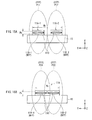
- the fly-eye lenses 40 A and 40 B which constitute the integrator 40 , each include multiple lens parts (or cells) arranged in a predetermined formation, which is a 4 ⁇ 3 (length ⁇ width) matrix form in this embodiment as shown in exemplary FIGS. 13A and 13B .
- the cells 42 in the fly-eye lens 40 B are positioned opposite the corresponding cells 41 in the fly-eye lens 40 A, respectively.
- the fly-eye lens 40 A is positioned at or around the focal positions of the fly-eye lens 40 B, while the fly-eye lens 40 B is positioned at or around the focal positions of the fly-eye lens 40 A.
- the fly-eye lens 40 A is 40 B which is located facing the projected image, thereby forming secondary light source surfaces or light source images.
- This secondary light source surfaces are positioned on a conjugate plane of the incident pupil in the projection optical system 70 .
- this secondary light source surfaces may not be positioned on the conjugate plane of the incident pupil in the projection optical system 70 precisely. Alternatively, it may be simply positioned within an allowable design range.
- the fly-eye lenses 40 A are 40 B may be integrated, that is, may be implemented by a single lens.
- any of the light beams from the light sources 10 A, 10 B, and 10 C exhibits non-uniform intensity distribution on a plane perpendicular to a travel direction thereof. If such a light beam is led to the illumination region 60 A (or the irradiated surface), then the illumination distribution thereon may also be non-uniform. As described above, the light beam from the light sources 10 A, 10 B, and 10 C is converted into the multiple light beams. Then, the light beams are led to the illumination region 60 A and overlapped thereon. This enables the illumination distribution on the illumination region 60 A to be made uniform.
- the condenser lens 50 has a function of converging the light beams from the integrator 40 , so that the illumination region 60 A is irradiated while the converged light beams are overlapped thereon.
- the spatial modulation device 60 has a function of subjecting the light beams from the illumination optical system 1 A to the two-dimensional modulation, based on color image signals corresponding to the wavelengths of the light beams from the light sources 10 A, 10 B, and 10 C. This makes it possible to create optical images.
- This spatial modulation device 60 may be a light-transmitting device as shown in FIGS. 2A and 2B .
- One example thereof is a light-transmitting type liquid crystal panel.
- the light sources 10 A, 10 B, and 10 C have total three or more light-emitting spots 11 B, the light sources emit the light beams of two or more wavelengths (R, G and B light beams in this embodiment). Moreover, at least one of the light sources 10 A, 10 B, and 10 C (called a “first light source” herein) is provided with the multiple light-emitting spots 11 B for emitting the light beams of the same wavelength (one of R, G, and B light beams in this embodiment) from the solid-state light-emitting device 11 .
- three or more of the light-emitting spots are provided within the whole of one or more light sources, to allow the whole of one or more light sources to emit light beams in two or more wavelength bands different from one another, and the solid-state light emitting device in a first light source which is at least one of the one or more light sources, has a plurality of light-emitting spots which emit light in the same wavelength band.
- red light-emitting spots 11 Br, green light-emitting spots 11 Bg, and blue light-emitting spots 11 Bb are placed on the light sources 10 A, 10 B, and 10 C.
- the light source 10 A has a single R light-emitting spot 11 Br on the solid-state light-emitting device 11 .
- the light source 10 B which corresponds to the first light source, has two green light-emitting spots 11 Bg thereon.
- the light source 10 C has a single B light-emitting spot 11 Bb thereon.
- the light source 10 A which corresponds to the first light source, has two R light-emitting spots 11 Br on the solid-state light-emitting device 11 .
- the light source 10 B which also correspond to the first light source, has two G light-emitting spots 11 Bg thereon.
- the light source 10 C which also correspond to the first light source, has two B light-emitting spots 11 Bb thereon.
- the light source 10 A has a single R light-emitting spot 11 Br on the solid-state light-emitting device 11 .
- the light source 10 B which corresponds to the first light source, has two G light-emitting spots 11 Bg thereon.
- the light source 10 C which also corresponds to the first light source, has two G light-emitting spots 11 Bg and a single B light-emitting spot 11 Bb thereon.
- the light source 10 C has, in addition to the multiple light-emitting spots for emitting light beams of the same wavelength (G light beams in this embodiment), the one or more light-emitting spots for emitting light beams of a wavelength different from the same wavelength on the device 11 (B light beam in this embodiment).
- the second light source may be the first light source or may be independent of it. In this case, it is preferable that the second light source have the following structure.
- the minor axes of the far field patterns (FFPs) of the light beams from the light-emitting spots 11 B are aligned or substantially aligned with the minor axis on a plane perpendicular to the optical axis of the optical member.
- the optical member is the integrator 40 of FIGS.
- the minor axes of the FFPs of the light beams from the light-emitting spots 11 B are aligned or substantially aligned with the Y axis (on the XY plane perpendicular to the Z axis) (i.e., the direction of the minor axis of the FFP in light emitted from each of the light-emitting spots substantially agrees with the direction of the minor axis of the optical member in a plane perpendicular to the optical axis of the optical member).
- the minor axes of the FFPs of the light beams from the light-emitting spot 11 B in the second light source are aligned or substantially aligned with the minor axis of the outer shape (or the rectangular case) of the projector 1 .
- the second light source emits light beams of different wavelengths, then it is preferable that the major axes of FFPs of the light beams having different wavelengths from the light-emitting spots 11 B be aligned or substantially aligned with each other.
- FIGS. 15A and 15B show exemplary second light sources.
- the second light source of FIG. 15A has two chips 11 A- 1 and 11 A- 2 that both are formed of LDs, and the chips are provided with light-emitting spots (or near field patterns (NFPs)) 11 B- 1 and 11 B- 2 including active layers 110 , respectively.
- NFPs near field patterns
- the second light source of FIG. 15B has a monolithic structure.
- This light source has the single chip 11 A formed of an LD, and the chip 11 A is provided with two light-emitting spots 11 B- 1 and 11 B- 2 thereon.
- the light-emitting spots 11 B- 1 and 11 B- 2 may emit light beams of the same wavelength or different wavelengths.
- the minor axes (parallel to the Y axes in this figure) of FFPs are aligned with the minor axis (parallel to the Y axis) on a plane perpendicular to the optical axis of the integrator 40 .
- the major axes (parallel to the X axes in this figure) of FFPs of the light beams from the light-emitting spots 11 B- 1 and 11 B- 2 are aligned with each other.
- the individual focal distances of the coupling lenses 20 A, 20 B, and 20 C and of the fly-eye lenses 40 A and 40 B be set such that the sizes of light source images S which the cells 41 of the fly-eye lens 40 A forms on the fly-eye lens 40 B are not larger than the sizes of the corresponding cells 42 of the fly-eye lens 40 B, respectively.
- each of the cells in fly-eye lenses 40 A and 40 B has a lateral/vertical length ratio (or an aspect ratio) other than 1, and this arrangement will be described in detail later.
- h 1 P 1 ⁇ ( f FEL /f CL1 ) ⁇ h FEL2
- h 2 P 2 ⁇ ( f FEL /f CL2 ) ⁇ h FEL2
- h 3 P 3 ⁇ ( f FEL /f CL3 ) ⁇ h FEL2 (3)
- h 1 denotes a size of a light source image S (light source image S 1 ) created by a light beam from the light source 10 A,
- h 2 denotes a size of a light source image S (light source image S 2 ) created by a light beam from the light source 10 B,
- h 3 denotes a size of a light source image S (light source image S 3 ) created by a light beam from the light source 10 C,
- P 1 denotes a size of a light emission region in the solid-state light-emitting device 11 contained in the light source 10 A
- P 2 denotes a size of a light emission region in the solid-state light-emitting device 11 contained in the light source 10 B,
- P 3 denotes a size of a light emission region in the solid-state light-emitting device 11 contained in the light source 10 C,
- f FEL denotes a focal distance of the fly-eye lenses 40 A and 40 B
- f CL1 denotes a focal distance of the coupling lens 20 A
- f CL2 denotes a focal distance of the coupling lens 20 B
- f CL3 denotes a focal distance of the coupling lens 20 C
- h FEL2 denotes a size of each cell 42 in the fly-eye lens 40 B.
- the P 1 is equal to the size of the light-emitting spot 11 B in the chip 11 A.
- the P 2 is equal to the size of the light-emitting spot 11 B in the chip 11 A.
- the P 3 is equal to the size of the light-emitting spot 11 B in the chip 11 A.
- the P 1 is equal to the size of the region defined by the outer frame of the light-emitting spots 11 B of the chips 11 A when all the chips 11 A are tiled with a minimum area.
- the P 2 is equal to the size of the region defined by the outer frame of the light-emitting spots 11 B of the chips 11 A when all the chips 11 A are tiled with a minimum area.
- the P 3 is equal to the size of the region defined by the outer frame of the light-emitting spots 11 B of the chips 11 A when all the chips 11 A are tiled with a minimum area.
- the coupling lens 20 A is formed by a combination of multiple lenses
- the f CL1 corresponds to a combined focal distance of these lenses.
- the coupling lens 20 B is formed by a combination of multiple lenses
- the f CL2 corresponds to a unified focal distance of these lenses.
- the coupling lens 20 C is formed by a combination of multiple lenses, then the f CL3 corresponds to a unified focal distance of these lenses.
- W 1 denotes a size of the solid-state light-emitting device 11 in the light source 10 A
- W 2 denotes a size of the solid-state light-emitting device 11 in the light source 10 B
- W 3 denotes a size of the solid-state light-emitting device 11 in the light source 10 C.
- the W is equal to the size of the chip 11 A itself. Meanwhile, the device 11 is composed of the multiple chips 11 A, the W is equal to the size of an area defined by tiling all the chips 11 A.
- the respective focal distances of the coupling lenses 20 A, 20 B and 20 C and of the fly-eye lenses 40 A and 40 B have the relationship defined by the following equations (7) to (12).
- ratios of vertical and horizontal focal distances (or anamorphic ratio) in the coupling lenses 20 A, 20 B and 20 C (f CL1H /f CL1V , f CL2H /f CL2V , and f CL3H /f CL3V ) be each equal to the reciprocal of a ratio of vertical and horizontal lengths of each cell 42 in the fly-eye lens 40 B (h FEL2V /h FEL2H ).
- the illumination optical system 1 A employ an anamorphic optical system. For example, consider that each cell 42 of the fly-eye lens 40 B has a rectangular shape, and its long side extends along a first direction such as a horizontal direction.
- the focal distances f CL1V , f CL2V , and f CL3V of the coupling lenses 20 A, 20 B and 20 C be longer than the focal distances f CL1H , f CL2H , and f CL3H thereof, respectively.
- the relationship represented by the equations (7) to (12) is illustrated in FIG. 16 .
- h 1H P 1H ⁇ ( f FELH /f CL1H ) ⁇ h FEL2H (7)
- h 2H P 2H ⁇ ( f FELH /f CL2H ) ⁇ h FEL2H (8)
- h 3H P 3H ⁇ ( f FELH /f CL3H ) ⁇ h FEL2H (9)
- h 1V P 1V ⁇ ( f FELV /f CL1V ) ⁇ h FEL2V (10)
- h 2V P 2V ⁇ ( f FELV /f CL2V ) ⁇ h FEL2V (11)
- h 3V P 3V ⁇ ( f FELV /f CL3V ) ⁇ h FEL2V (12) where
- h 1H denotes a size (width) of a light source image S (light source image S 1 ) along a first direction (for example, the horizontal direction), which is created by a light beam from the light source 10 A,
- h 2H denotes a size (width) of a light source image S (light source image S 2 ) along the first direction (for example, the horizontal direction), which is created by a light beam from the light source 10 B,
- h 3H denotes a size (width) of a light source image S (light source image S 3 ) along the first direction (for example, the horizontal direction), which is created by a light beam from the light source 10 C,
- h 1V denotes a size (width) of a light source image S (light source image S 2 ) along a second direction perpendicular to the first direction (for example, the vertical direction), which is created by a light beam from the light source 10 A,
- h 2V denotes a size (width) of a light source image S (light source image S 2 ) along the second direction (for example, the vertical direction), which is created by a light beam from the light source 10 B,
- h 3V denotes a size (width) of a light source image S (light source image S 3 ) along the second direction (for example, the vertical direction), which is created by a light beam from the light source 10 C,
- P 1H denotes a size (width) of the light emission region along the first direction or a direction corresponding thereto, which is located on the solid-state light-emitting device 11 contained in the light source 10 A,
- P 2H denotes a size (width) of the light emission region along the first direction or the direction corresponding thereto, which is located on the solid-state light-emitting device 11 contained in the light source 10 B,
- P 3H denotes a size (width) of the light emission region along the first direction or a direction corresponding thereto, which is located on the solid-state light-emitting device 11 contained in the light source 10 C,
- P 1V denotes a size (width) of the light emission region along the second direction or the direction corresponding thereto, which is located on the solid-state light-emitting device 11 contained in the light source 10 A,
- P 2V denotes a size (width) of the light emission region along the second direction or the direction corresponding thereto, which is located on the solid-state light-emitting device 11 contained in the light source 10 B,
- P 3V denotes a size (width) of the light emission region along the second direction or a direction corresponding thereto, which is located on the solid-state light-emitting device 11 contained in the light source 10 C,
- f FELH denotes a focal distance of the fly-eye lenses 40 A and 40 B in the first direction
- f FELV denotes a focal distance of the fly-eye lenses 40 A and 40 B in the second direction
- f CL1H denotes a focal distance of the coupling lens 20 A in the first direction or the direction corresponding thereto
- f CL2H denotes a focal distance of the coupling lens 20 B in the first direction or the direction corresponding thereto
- f CL3H denotes a focal distance of the coupling lens 20 C in the first direction or the direction thereto
- f CL1V denotes a focal distance of the coupling lens 20 A in the second direction or the direction corresponding thereto
- f CL2V denotes a focal distance of the coupling lens 20 B in the second direction or a direction corresponding thereto
- f CL3V denotes a focal distance of the coupling lens 20 C in the second direction or a direction corresponding thereto
- h FEL2H denotes a size (width) of one of the cells 42 in the fly-eye lens 40 B along the first direction
- h FEL2V denotes a size (width) of one of the cells 42 in the fly-eye lens 40 B along the second direction.
- the “first direction or a direction corresponding thereto” represents the first direction, if the light sources 10 A, 10 B, and 10 C, and the coupling lenses 20 A, 20 B and 20 C are aligned with the optical axis of the integrator 40 .
- the “first direction or a direction corresponding thereto” represents the direction corresponding to the first direction, if light sources 10 A, 10 B, and 10 C and the coupling lenses 20 A, 20 B and 20 C are not aligned with the optical axis of the integrator 40 .
- the direction corresponding to the first direction is determined based on the layout of the optical devices on the optical paths between the respective light sources 10 A, 10 B, and 10 C and the integrator 40 .
- the “second direction or a direction corresponding thereto” represents the second direction, if the light sources 10 A, 10 B, and 10 C, and the coupling lenses 20 A, 20 B and 20 C are aligned with the optical axis of the integrator 40 .
- the “second direction or a direction corresponding thereto” represents the direction corresponding to the second direction, if light sources 10 A, 10 B, and 10 C and the coupling lenses 20 A, 20 B and 20 C are not aligned with the optical axis of the integrator 40 .
- the direction corresponding to the second direction is determined based on the layout of the optical devices on the optical paths between the respective light sources 10 A, 10 B, and 10 C and the integrator 40 .
- the P 1H is equal to the size (width) of the light-emitting spot 11 B on the chip 11 A along the first direction or the direction corresponding thereto.
- the P 2H is equal to the size (width) of the light-emitting spot 11 B on the chip 11 A along the first direction or the direction corresponding thereto.
- the P 3H is equal to the size (width) of the light-emitting spot 11 B on the chip 11 A along the first direction or the direction corresponding thereto.
- the P 1H is equal to the size (width) of an area, along the first direction or the direction corresponding thereto, which is defined by the outer frame of the light-emitting spots 11 B of the chips 11 A when all the chips 11 A are tiled with a minimum area.
- the P 2H is equal to the size (width) of an area, along the first direction or the direction corresponding thereto, which is defined by the outer frame of the light-emitting spots 11 B of the chips 11 A when all the chips 11 A are tiled with a minimum area.
- the P 3H is equal to the size (width) of an area, along the first direction or the direction corresponding thereto, which is defined by the outer frame of the light-emitting spots 11 B of the chips 11 A when all the chips 11 A are tiled with a minimum area.
- the P 1V is equal to the size (width) of the light-emitting spot 11 B on the chip 11 A along the second direction or the direction corresponding thereto.
- the P 2V is equal to the size (width) of the light-emitting spot 11 B on the chip 11 A along the second direction or the direction corresponding thereto.
- the P 3V is equal to the size (width) of the light-emitting spot 11 B on the chip 11 A along the second direction or the direction corresponding thereto.
- the P 1V is equal to the size (width) of an area, along the second direction or the direction corresponding thereto, which is defined by the outer frame of the light-emitting spots 11 B of the chips 11 A when all the chips 11 A are tiled with a minimum area.
- the P 2V is equal to the size (width) of an area, along the second direction or the direction corresponding thereto, which is defined by the outer frame of the light-emitting spots 11 B of the chips 11 A when all the chips 11 A are tiled with a minimum area.
- the P 3V is equal to the size (width) of an area, along the second direction or the direction corresponding thereto, which is defined by the outer frame of the light-emitting spots 11 B of the chips 11 A when all the chips 11 A are tiled with a minimum area.
- each of the cells 41 and 42 in the fly-eye lenses 40 A and 40 B has an aspect ratio other than 1, then it is preferable that the aspect ratios of each cell 41 in the fly-eye lens 40 A and of the illumination region 60 A have a relationship defined by the following equation (13).
- the aspect ratio (H/V) (see FIG. 17 ) of the illumination region 60 A is correlated with the resolution of the spatial modulation device 60 .
- the resolution (VGA) of the spatial modulation device 60 is 640 ⁇ 480
- the aspect ratio (H/V) of the illumination region 60 A is 640/480.
- the resolution (WVGA) of the spatial modulation device 60 is 800 ⁇ 480
- the (H/V) of the illumination region 60 A is 800/480.
- h FEL1H /h FEL1V H/V (13) where
- h FEL1H denotes a size (width) of each cell in the fly-eye lens 40 A along the first direction
- h FEL1V denotes a size (width) of each cell in the fly-eye lens 40 A in the second direction
- H denotes a size (width) of the illumination region 60 A along the first direction
- V denotes a size (width) of the illumination region 60 A along the second direction.
- the focal distances and numerical apertures (NAs) of the coupling lenses 20 A, 20 B and 20 C be set such that the size of light beams incident on the coupling lenses 20 A, 20 B and 20 C is not larger than the size of these coupling lenses.
- ⁇ CL1 denotes a size of a light beam incident on the coupling lens 20 A
- ⁇ CL2 denotes a size of a light beam incident on the coupling lens 20 B
- ⁇ CL3 denotes a size of a light beam incident on the coupling lens 20 C
- NA 1 denotes an NA of the coupling lens 20 A
- NA 2 denotes an NA of the coupling lens 20 B
- NA 3 denotes an NA of the coupling lens 20 C
- h CL1 denotes a size of the coupling lens 20 A
- h CL2 denotes a size of the coupling lens 20 B
- h CL3 denotes a size of the coupling lens 20 C.
- the coupling lenses 20 A, 20 B and 20 C have the aspect ratio other than 1, then it is preferable that the focal distances and NAs of the coupling lenses 20 A, 20 B and 20 C have a relationship defined by the following equations (17) to (22).
- ⁇ CL1H denotes a size (width) of a light beam incident on the coupling lens 20 A along the first direction (for example, the horizontal direction) or the direction corresponding thereto,
- ⁇ CL2H denotes a size (width) of a light beam incident on the coupling lens 20 B along the first direction (for example, the horizontal direction) or the direction corresponding thereto,
- ⁇ CL3H denotes a size (width) of a light beam incident on the coupling lens 20 C along the first direction (for example, the horizontal direction) or the direction corresponding thereto,
- ⁇ CL1V denotes a size (width) of a light beam incident on the coupling lens 20 A along the second direction (for example, the vertical direction) or the direction corresponding thereto,
- ⁇ CL2V denotes a size (width) of a light beam incident on the coupling lens 20 B along the second direction (for example, the vertical direction) or the direction corresponding thereto,
- ⁇ CL3V denotes a size (width) of a light beam incident on the coupling lens 20 C along the second direction (for example, the vertical direction) or the direction corresponding thereto,
- NA 1H denotes an NA of the coupling lens 20 A along the first direction or the direction corresponding thereto
- NA 2H denotes an NA of the coupling lens 20 B along the first direction or the direction corresponding thereto
- NA 3H denotes an NA of the coupling lens 20 C along the first direction or the direction corresponding thereto
- NA 1V denotes an NA of the coupling lens 20 A along the second direction or the direction corresponding thereto
- NA 2V denotes an NA of the coupling lens 20 B along the second direction or the direction corresponding thereto
- NA 3V denotes an NA of the coupling lens 20 C along the second direction or the direction corresponding thereto
- h CL1H denotes a size (width) of the coupling lens 20 A along the first direction or the direction corresponding thereto,
- h CL2H denotes a size (width) of the coupling lens 20 B along the first direction or the direction corresponding thereto,
- h CL3H denotes a size (width) of the coupling lens 20 C along the first direction or the direction corresponding thereto,
- h CL1V denotes a size (width) of the coupling lens 20 A along the second direction or the direction corresponding thereto,
- h CL2V denotes a size (width) of the coupling lens 20 B along the second direction or the direction corresponding thereto, and
- h CL3V denotes a size (width) of the coupling lens 20 C along the second direction or the direction corresponding thereto.
- all the light sources 10 A, 10 B, and 10 C are provided with the solid-state light-emitting devices 11 on which the total three or more light-emitting spots 11 B are formed.
- the light beams of two or more different wavelengths red, green, and blue light beams in the embodiment
- the solid-state light-emitting device 11 has the multiple light-emitting spots 11 B from which the light beams of the same wavelength (any of red, green, and blue light beams in the embodiment) are emitted.
- the three or more of the light-emitting spots are provided within the whole of one or more light sources, to allow the whole of one or more light sources to emit the light beams in the two or more wavelength bands different from one another, and the solid-state light emitting device in the first light source which is at least one of the one or more light sources, has the plurality of light-emitting spots which emit the light in the same wavelength band.
- a typical projector is designed to display color images by using light beams of three primary colors, such as red, green, and blue light beams.
- three primary colors such as red, green, and blue light beams.
- intensities or luminance properties may be different for the respective colors among devices (or chips in a solid-state light-emitting device) which emit the light beams of the three primary colors, respectively.
- the light beam of the lower intensity needs to be used as a reference. For example, if the green light beam is darker than the red and blue light beams, then the luminance of the red and blue light beams needs to be adjusted or adapted to that of the green light upon white balance adjustment.
- the projector 1 has the light sources 10 A, 10 B, and 10 C configured above.
- the light beams in two or more wavelength bands here, red light, green light, and blue light
- the illumination optical system 1 A as the illumination light
- the plurality of light-emitting spots 11 B which emit the light in the same wavelength band are provided in at least one of the one or more light sources (for example, the first light source).
- At least one of the light sources 10 A, 10 B, and 10 C may be provided with the solid-state light-emitting devices 11 on which the multiple light-emitting spots 11 B are formed on the multiple chips 11 A composed of LDs.
- the projector 1 of this structure provides the following operations and effects.
- the minor axes of FFPs of the light beams from the light-emitting spots 11 B may be adjusted to be substantially aligned with the minor axis on a plane perpendicular to the optical axis of the integrator 40 . Because of this adjustment, the minor axes of FFPs of the light beams from the light-emitting spots 11 B are also substantially aligned with the minor axis of the outer case of the projector 1 . This contributes to further compactness of the projector 1 .
- the major axes of FFPs of the light beams from the light-emitting spots 11 B are adjusted to be substantially aligned with one another.
- using an I-cut lens makes it possible to decrease the loss of the light beam in the illumination optical system of the projector 1 .
- an optical effective range may be sacrificed in portions subjected to “I-cut”.
- the light loss is advantageously reduced by matching the one axes of FFPs of light beams from the LDs with a direction to which the “I-cut” is performed (a direction in which an effective diameter is wide).
- the focal distances (f CL1 , f CL2 , f CL3 , and f FEL ) of the coupling lenses 20 A, 20 B and 20 C and of the fly-eye lenses 40 A and 40 B may be set such that the sizes of the light source images which the cells 41 of the fly-eye lens 40 A forms on the fly-eye lens 40 B are not larger than the sizes of the corresponding cells 42 of the fly-eye lens 40 B.
- the projector 1 of this structure gives the following operations and effects.
- the solid-state light-emitting device 11 is adapted to emit one or more light beams from the light emission region including one or more light-emitting spots of a dot or non-dot shape, and this device 11 is formed by one or more LEDs, OELDs or LDs. Therefore, even if the fly-eye lens 40 B is positioned at the focal positions of the fly-eye lens 40 A, the light source images S which the cells of the fly-eye lens 40 A form on the fly-eye lens 40 B are not perfect dot-shape, and each of the images S has a considerable size (see FIG. 16 ).
- the projector 1 of this embodiment since it is unlikely that one light source image S is formed across the plurality of cells, the light incident on the fly-eye lens 40 B reaches the illumination region 60 A efficiently. It is thus possible to improve the light use efficiency of the illumination optical system 1 A.
- each of the cells 41 and 42 in the fly-eye lenses 40 A and 40 B has an aspect ratio other than 1, then the focal distances (f CL1H , f CL2H , f CL3H , f CL1V , f CL2V , f CL3V , f FELH , and f FELV ) of the coupling lenses 20 A, 20 B and 20 C and the focal distances (f FELH and f FELV ) of the fly-eye lenses 40 A and 40 B may be set in consideration of this aspect ratio. It is thus possible to further improve the light use efficiency of the illumination optical system 1 A.
- the coupling lenses 20 A, 20 B and 20 C have an aspect ratio other than 1, then the focal distances (f CL1H , f CL2H , f CL3H , f CL1V , f CL2V , and f CL3V ) and the NAs (NA 1H , NA 2H , NA 3H , NA 1V , NA 2V , and NA 3V ) of the coupling lenses 20 A, 20 B and 20 C may be set in consideration of this aspect ratio. It is thus possible to further improve the light use efficiency of the illumination optical system 1 A.
- the traveling-direction-angles of the light sources 10 A, 10 B, and 10 C differ from one another, then the focal distances (f CL1H , f CL2H , f CL3H , f CL1V , f CL2V , and f CL3V ) and the NAs (NA 1H , NA 2H , NA 3H , NA 1V , NA 2V , and NA 3V ) of the coupling lenses 20 A, 20 B and 20 C may be set in consideration on this difference. It is thus possible to further improve the light use efficiency of the illumination optical system 1 A.
- FIGS. 18A and 18B show a schematic structure of a projector according to a second embodiment of the technology (called a “projector 3 ” herein). Note that this projector 3 corresponds to a concrete example of the “projection display unit” according to one embodiment of the technology.
- FIG. 18A shows the schematic structure of the projector 3 as seen from the above or on a Y axis, and FIG. 18B shows it as seen from one side or on an X axis.
- a structure of the projector 3 differs from that of the projector 1 in the spatial modulation device and illumination optical system.
- the projector 3 includes a reflective spatial modulation device 60 and an illumination optical system 3 A. Accordingly, a description of the projector 3 will be mainly focused on different points from the projector 1 , and the same points will be omitted as deemed appropriate.
- the illumination optical system 3 A of the projector 3 includes a condenser lens 50 A instead of the condenser lens 50 of the illumination optical system 1 A in the projector 1 .
- This condenser lens 50 A has a function of converting the light beams from the integrator into collimated light beams and delivering the beams to a condenser lens 50 B through a polarization beam splitter 51 .
- the spatial modulation device 60 may be implemented by a reflective device such as a reflective liquid crystal panel. Therefore, the projector 3 further includes the condenser lens 50 B and the polarization beam splitter 51 in contrast to the projector 1 .
- the polarization beam splitter 51 is an optical device which has a function of selectively allowing incident light to pass through or be reflected. Specifically, once light is incident on the polarization beam splitter 51 , a specific polarized component, such as a P-polarized component, in the incident light passes through and the other polarized component, such as an S-polarized component, is reflected.
- the spatial modulation device 60 has a function of modulating the incident light beam and reflecting the incident light beam while changing the polarization thereof.
- the condenser lens 50 B has a function of focusing the light beams from the light sources through the integrator 40 , condenser lens 50 A, and polarization beam splitter 51 , so that the focused light beams are irradiated on the illumination region 60 A while being overlapped thereon.
- the projector 3 of this embodiment configured above has substantially the same behavior as the projector 1 of the first embodiment does. Therefore, the projector provides substantially the same effects as the projector does.
- the width along the X axis on a plane (XY plane) perpendicular to the optical axis of the integrator 40 is relatively long, in particular.
- the projector 3 as a whole is further advantageously made compact.
- FIGS. 19A and 19B show a schematic structure of a projector according to a third embodiment of the technology (called a “projector 4 ” herein). Note that this projector 4 corresponds to a concrete example of the “projection display unit” according to one embodiment of the technology.
- FIG. 19A shows the schematic structure of the projector 4 as seen from the above or the X axis
- FIG. 19B shows it as seen from one side or the Y axis.
- FIG. 20A shows the optical paths as seen from the top of the projector 4 or on the Y axis
- FIG. 20B shows the optical paths as seen from the side of the projector 4 or on the Y axis.
- a structure of the projector 4 of this embodiment differs from that of the projector 1 in the illumination optical system.
- the projector 4 includes an illumination optical system 4 A. Accordingly, a description of the projector 4 will be mainly focused on different points from the projector 1 , and the same points will be omitted as deemed appropriate.
- the illumination optical system 4 A of the projector 4 does not include the light sources 10 A, 10 B, and 10 C and the dichroic mirrors 30 A and 30 B, but includes a light source 10 D instead.
- This light source 10 D is placed on the optical axis of a coupling lens 20 D.
- the illumination optical system 4 A is configured such that a light beam from the light source 10 D directly enters the coupling lens 20 D.
- the light source 10 D includes, but not limited to, the solid-state light-emitting device 11 and a package 12 in which the device 11 mounted on a substrate material is supported and covered.
- the device 11 may be composed of the one or more chips 11 A of the upper surface emitting type.
- the light source 10 D may have a can shape.
- the light source 10 D may include the stem 13 , the cap 14 , and the solid-state light-emitting device 11 located within an inner space defined by the stem 13 and the cap 14 .
- the device 11 may be composed of the one or more chips 11 A of the side surface emitting type.
- the solid-state light-emitting device 11 in the light source 10 D has the light emission region composed of the one or more light-emitting spots of a dot or non-dot shape, and from this the light emission region, the light beam is emitted.
- the solid-state light-emitting device 11 in the light source 10 D may be composed of the single chip 11 A for emitting a light beam of a predetermined wavelength, or the multiple chips 11 A for emitting light beams of the same wavelength or different wavelengths. If the device 11 is composed of the multiple chips 11 A, then the chips 11 A may be arranged laterally in a line or arranged in a matrix form.
- the chip 11 A may be an LED, OLED, or LD. If the solid-state light-emitting device 11 in the light source 10 D is composed of the multiple chips 11 A, then all the chips 11 A may be LEDs, OLEDs, or LDs. Alternatively, the chips 11 A may be a combination of LEDs and OLEDs, LEDs and LDs, or OLEDs and LDs. In any case, however, it is preferable that the chips 11 A include at least one LD.
- the chips 11 A may be ones for emitting light beams of the same wavelength or different wavelengths. Moreover, all of the chips 11 A may be ones for emitting light beams having a wavelength of 400 nm to 500 nm (B), 500 nm to 600 nm (G), or 600 nm to 700 nm (R). Furthermore, the chips 11 A may be a combination of ones for emitting light beams having a wavelength of 400 nm to 500 nm (B), 500 nm to 600 nm (G), and 600 nm to 700 nm (R).
- the solid-state light-emitting device 11 in the light source 10 D has total three or more light-emitting spots from which light beam of two or more different wavelengths (R, G, and B light beams) are emitted, similarly to the light sources 10 A, 10 B, and 10 C of the first embodiment.
- the light source 10 D serves as the first light source.
- the solid-state light-emitting device 11 in the light source 10 D includes the multiple light-emitting spots from which light beams of the same wavelength (one of R, G, and B light beams) are emitted.
- the solid-state light-emitting device 11 in the light source 10 D has an R light-emitting spot 11 Br, two G light-emitting spots 11 Bg, and a B light-emitting spot 11 Bb.
- the device 11 in the light source 10 D (first light source) is provided with, in addition to the multiple light-emitting spots for emitting light beams of the same wavelength (G light-emitting spots 11 Bg in this embodiment), one or more light-emitting spots for emitting light beams of different wavelengths from the same wavelength (R light-emitting spot 11 Br and B light-emitting spot 11 Bb in this embodiment). Consequently, the projector 4 of this embodiment configured above has substantially the same behavior as the projector 1 of the first embodiment does. Therefore, the projector 4 provides substantially the same effects as the projector 1 does.
- FIGS. 22A to 22C schematically show exemplary arrangements of light-emitting spots (R light-emitting spots 11 Br, G light-emitting spots 11 Bg, and B light-emitting spots 11 Bb) formed on individual light sources in a projector of modification 1.
- the solid-state light-emitting device 11 in the light source 10 A has an R light-emitting spot 11 Br.
- the device 11 in the light source 10 B which serves as the first light source, has two G light-emitting spots 11 Bg and a B light-emitting spot 11 Bb.
- the device 11 in the light source 10 B (first light source) has, in addition to the light-emitting spots for emitting the light beams of the same wavelength (G light-emitting spots 11 Bg), the one or more light-emitting spots for emitting the light beams of different wavelengths from the same wavelength (B light-emitting spot 11 Bb).
- the solid-state light-emitting device 11 in the light source 10 A has an R light-emitting spot 11 Br.
- the device 11 in the light source 10 B which serves as the first light source, has two G light-emitting spots 11 Bg and two B light-emitting spots 11 Bb.
- the device 11 in the light source 10 B has, in addition to the light-emitting spots for emitting the light beams of the same wavelength (G light-emitting spots 11 Bg or B light-emitting spots 11 Bb), the one or more light-emitting spots for emitting the light beams of different wavelengths from the same wavelength (two B light-emitting spots 11 Bb or two G light-emitting spots 11 Bg).
- the solid-state light-emitting device 11 in the light source 10 A has an R light-emitting spot 11 Br.
- the device 11 in the light sources 10 B and 10 C, each of which serves as the first light source have two G light-emitting spots 11 Bg and two B light-emitting spots 11 Bb, respectively.
- the device 11 in the light source 10 D has a B light-emitting spot 11 Bb. Note that the plurality of first light sources (two light sources 10 B and 10 C in this modification) are provided in the case of FIG. 22A .
- the arrangement of the light-emitting spots which the light sources are provided with in the illumination optical system is not limited, and the colors or wavelengths of light beams from the light-emitting spots are not limited either. It is therefore possible to modify the arrangement of the light-emitting spots appropriately in accordance with an application or requirement. Even if the arrangement is modified, the behaviors of a projector having this arrangement are not changed. It is therefore possible for the projector to provide the same effects as the projectors of the embodiments do.
- FIG. 23 shows a cross section of an exemplary structure of a light source (one of the light sources 10 A, 10 B, 10 C, and 10 D) in a projector of modification 2.
- a light source of this modification differs from the light sources of the embodiments in that at least one of the chips 11 A is disposed in a slanting direction to an optical axis Z 1 in the second light source.
- the chips 11 A- 1 and 11 A- 2 are disposed in a slanting direction to the optical axis Z 1 .
- the chip 11 A- 2 is positioned parallel to the optical axis Z 1 . Accordingly, the light beam from the chip 11 A- 2 travels parallel to the optical axis Z 1 , while those from the chips 11 A- 1 and 11 A- 3 travel at any angles with respect thereto.
- the intensity of the single light beam is peaked on the optical axis Z 1 .
- the minor axes of FFPs of the laser beams from the light-emitting spots 11 B- 1 , 11 B- 2 , and 11 B- 3 on the chips 11 A- 1 , 11 A- 2 , and 11 A- 3 respectively be substantially aligned with the minor axis (Y axis in this modification) on a plane perpendicular to the optical axis of the integrator 40 .
- the light source of this modification serves as the second light source, that is, this light source emits light beams of two or more different wavelengths
- the major axes (X axis in this modification) of FFPs of the light beams having the different wavelengths among the light beams from all the light-emitting spots 11 B- 1 , 11 B- 2 , and 11 B- 3 be substantially aligned with each other.
- FIGS. 25A and 25B show a schematic structure of a projector of modification 3 (called a “projector 6 ” herein). Note that this projector 6 corresponds to a concrete example of the “projection display unit” according to one embodiment of the technology.
- FIG. 25A shows the schematic structure of the projector 6 as seen from the above or the Y axis, and FIG. 25B shows it as seen from one side or the X axis.
- the structure of the projector 6 differs from that of the projector 1 of the first embodiment in the illumination optical system.
- the projector 6 includes an illumination optical system 6 A. Accordingly, a description of the projector 6 will be mainly focused on different points from the projector 1 , and the same points will be omitted as deemed appropriate.
- the structure of the illumination optical system 6 A in the projector 6 is equivalent to that of the illumination optical system 1 A in the projector 1 , if the integrator 40 and the condenser lens 50 are removed from the projector 1 .
- the illumination optical system 6 A is constituted by the light sources 10 A, 10 B, and 10 C, the coupling lenses 20 A, 20 B and 20 C, and the optical path unifying device 30 .
- the integrator 40 and the condenser lens 50 are options and may be removed from the illumination optical system 1 A as necessary.
- any of the illumination optical systems 1 A, 3 A, 4 A, and 5 A employs an infinity optical system in which the collimated light beam is incident on the fly-eye lens 40 A.
- the illumination optical systems are not limited to this structure.
- any of the illumination optical systems 1 A, 3 A, 4 A, and 5 A may employ a finite optical system in which a convergent or divergent light beam is incident on the fly-eye lens 40 A, instead of the infinity optical system.
- traveling-direction angle conversion devices which have a function of converging or diverging the light beams from the light sources 10 A to 10 D may be provided in any of the illumination optical systems 1 A, 3 A, 4 A, and 5 A of the embodiments, instead of the coupling lens 20 A to 20 D, respectively.
- the optical magnification of an optical system including the traveling-direction angle conversion devices and the fly-eye lenses 40 A and 40 B be set such that the sizes of the light source images S which the cells 41 of the fly-eye lens 40 A forms on the fly-eye lens 40 B are not larger than the sizes of the corresponding cells 42 of the fly-eye lens 40 B.
- the optical magnification of the optical system including the traveling-direction angle conversion devices and the fly-eye lenses 40 A and 40 B have a relationship defined by the following equation.
- the cells 41 and 42 of the fly-eye lenses 40 A and 40 B have an aspect ratio other than 1, then the illumination optical system 1 A, 3 A, 4 A, and 5 A employ the anamorphotic optical system.
- h P ⁇ m ⁇ h FEL2
- m denotes optical magnification of an optical system including the traveling-direction angle conversion devices and the fly-eye lenses 40 A and 40 B.
- the illumination optical systems 1 A, 3 A, 4 A, 5 A and 6 A are applied to the projection display unit.
- the illumination optical systems 1 A, 3 A, 4 A, 5 A and 6 A are applicable to other display devices.
- any of the illumination optical systems 1 A, 3 A, 4 A, 5 A and 6 A is applicable to a rear-projection display device 7 .
- This rear-projection display device 7 includes any of the projectors 1 , 3 , 4 , 5 , and 6 having the illumination optical systems 1 A, 3 A, 4 A, 5 A, and 6 A, respectively and a transmissive screen 8 on which optical images to be projected by the projection optical system 70 are displayed.
- the luminance of the illumination light as a whole and the optical images is increased.
- the spatial modulation device 60 is implemented by a light-transmitting or reflective device.
- the spatial modulation device 60 may be a digital micro-mirror device.
- the illumination optical systems and the display devices do not need to include all the optical components or may further include one or more additional components.
- the illumination units are applied to the projection display units.
- the application of the illumination units is not limited to projection display units. Alternatively, it may be applied to exposure devices such as steppers.
Abstract
Description
h 1 =P 1×(f FEL /f CL1)≦h FEL2 (1)
h 2 =P 2×(f FEL /f CL2)≦h FEL2 (2)
h 3 =P 3×(f FEL /f CL3)≦h FEL2 (3)
where
h 1 =W 1×(f FEL /f CL1)≦h FEL2 (4)
h 2 =W 2×(f FEL /f CL2)≦h FEL2 (5)
h 3 =W 3×(f FEL /f CL3)≦h FEL2 (6)
where
h 1H =P 1H×(f FELH /f CL1H)≦h FEL2H (7)
h 2H =P 2H×(f FELH /f CL2H)≦h FEL2H (8)
h 3H =P 3H×(f FELH /f CL3H)≦h FEL2H (9)
h 1V =P 1V×(f FELV /f CL1V)≦h FEL2V (10)
h 2V =P 2V×(f FELV /f CL2V)≦h FEL2V (11)
h 3V =P 3V×(f FELV /f CL3V)≦h FEL2V (12)
where
h FEL1H /h FEL1V =H/V (13)
where
φCL1=2×f CL1×NA1 ≦h CL1 (14)
φCL2=2×f CL2×NA2 ≦h CL2 (15)
φCL3=2×f CL3×NA3 ≦h CL3 (16)
where
φCL1H=2×f CL1H×NA1H ≦h CL1H (17)
φCL2H=2×f CL2H×NA2H ≦h CL2H (18)
φCL3H=2×f CL3H×NA3H ≦h CL3H (19)
φCL1V=2×f CL1V×NA1V ≦h CL1V (20)
φCL2V=2×f CL2V×NA2V ≦h CL2V (21)
φCL3V=2×f CL3V×NA3V ≦h CL3V (22)
where
h=P×m≦h FEL2
where
Claims (13)
h=P×m≦h FEL2
Priority Applications (3)
| Application Number | Priority Date | Filing Date | Title |
|---|---|---|---|
| US14/296,986 US9374564B2 (en) | 2010-11-26 | 2014-06-05 | Illumination unit, projection display unit, and direct view display unit |
| US15/180,848 US9749602B2 (en) | 2010-11-26 | 2016-06-13 | Illumination unit, projection display unit, and direct view display unit |
| US15/668,277 US10162250B2 (en) | 2010-11-26 | 2017-08-03 | Illumination unit, projection display unit, and direct view display unit |
Applications Claiming Priority (2)
| Application Number | Priority Date | Filing Date | Title |
|---|---|---|---|
| JP2010263735A JP2012113223A (en) | 2010-11-26 | 2010-11-26 | Illuminating device, projection type display device, and direct-view type display device |
| JP2010-263735 | 2010-11-26 |
Related Child Applications (1)
| Application Number | Title | Priority Date | Filing Date |
|---|---|---|---|
| US14/296,986 Continuation US9374564B2 (en) | 2010-11-26 | 2014-06-05 | Illumination unit, projection display unit, and direct view display unit |
Publications (2)
| Publication Number | Publication Date |
|---|---|
| US20120133900A1 US20120133900A1 (en) | 2012-05-31 |
| US8770761B2 true US8770761B2 (en) | 2014-07-08 |
Family
ID=44970918
Family Applications (4)
| Application Number | Title | Priority Date | Filing Date |
|---|---|---|---|
| US13/276,818 Active 2032-06-12 US8770761B2 (en) | 2010-11-26 | 2011-10-19 | Illumination unit, projection display unit, and direct view display unit |
| US14/296,986 Active 2031-12-29 US9374564B2 (en) | 2010-11-26 | 2014-06-05 | Illumination unit, projection display unit, and direct view display unit |
| US15/180,848 Active US9749602B2 (en) | 2010-11-26 | 2016-06-13 | Illumination unit, projection display unit, and direct view display unit |
| US15/668,277 Active US10162250B2 (en) | 2010-11-26 | 2017-08-03 | Illumination unit, projection display unit, and direct view display unit |
Family Applications After (3)
| Application Number | Title | Priority Date | Filing Date |
|---|---|---|---|
| US14/296,986 Active 2031-12-29 US9374564B2 (en) | 2010-11-26 | 2014-06-05 | Illumination unit, projection display unit, and direct view display unit |
| US15/180,848 Active US9749602B2 (en) | 2010-11-26 | 2016-06-13 | Illumination unit, projection display unit, and direct view display unit |
| US15/668,277 Active US10162250B2 (en) | 2010-11-26 | 2017-08-03 | Illumination unit, projection display unit, and direct view display unit |
Country Status (4)
| Country | Link |
|---|---|
| US (4) | US8770761B2 (en) |
| EP (3) | EP2458875B1 (en) |
| JP (1) | JP2012113223A (en) |
| CN (1) | CN102566232B (en) |
Cited By (4)
| Publication number | Priority date | Publication date | Assignee | Title |
|---|---|---|---|---|
| US20140247591A1 (en) * | 2010-11-29 | 2014-09-04 | Sony Corporation | Illumination unit, projection display unit, and direct view display unit |
| US20140285773A1 (en) * | 2010-11-26 | 2014-09-25 | Sony Corporation | Illumination unit, projection display unit, and direct view display unit |
| US20150109773A1 (en) * | 2011-12-11 | 2015-04-23 | Appotronics Corporation Limited | Light source and illuminating device |
| US20210247678A1 (en) * | 2019-03-22 | 2021-08-12 | Nichia Corporation | Light source device and optical engine |
Families Citing this family (8)
| Publication number | Priority date | Publication date | Assignee | Title |
|---|---|---|---|---|
| JP5811807B2 (en) * | 2011-03-22 | 2015-11-11 | ソニー株式会社 | Illumination device, projection display device, direct view display device |
| JP5772143B2 (en) * | 2011-03-28 | 2015-09-02 | ソニー株式会社 | Illumination device, projection display device, and direct view display device |
| JP5648556B2 (en) * | 2011-03-28 | 2015-01-07 | ソニー株式会社 | Illumination device, projection display device, and direct view display device |
| US9116421B1 (en) * | 2012-01-07 | 2015-08-25 | Greenlight Optics, LLC | Projector with laser illumination elements offset along an offset axis |
| JP6108666B2 (en) * | 2012-02-13 | 2017-04-05 | キヤノン株式会社 | Image projection device |
| JP6380813B2 (en) * | 2015-12-24 | 2018-08-29 | カシオ計算機株式会社 | Light source device and projection device |
| JP2019138940A (en) * | 2018-02-06 | 2019-08-22 | セイコーエプソン株式会社 | Light source device, illumination device and projector |
| JP7311770B2 (en) * | 2018-12-12 | 2023-07-20 | 日亜化学工業株式会社 | Light-emitting module manufacturing method, light-emitting module, and projector |
Citations (14)
| Publication number | Priority date | Publication date | Assignee | Title |
|---|---|---|---|---|
| JPH11260144A (en) | 1998-03-12 | 1999-09-24 | Matsushita Electric Ind Co Ltd | Lens element, illumination optical system and projection-type display unit using the same |
| WO1999049358A1 (en) | 1998-03-26 | 1999-09-30 | Mitsubishi Denki Kabushiki Kaisha | Image display and light-emitting device |
| EP1184706A2 (en) | 2000-08-30 | 2002-03-06 | Dainippon Screen Mfg. Co., Ltd. | Illuminating apparatus |
| EP1347653A2 (en) | 2002-03-22 | 2003-09-24 | Seiko Epson Corporation | Image display device and projector |
| JP2004013021A (en) | 2002-06-10 | 2004-01-15 | Ricoh Co Ltd | Light source device, light source module, optical scanner, and image forming device |
| JP2004191735A (en) | 2002-12-12 | 2004-07-08 | Fuji Photo Film Co Ltd | Illumination optical system and exposure device |
| US20050018141A1 (en) | 2003-06-11 | 2005-01-27 | Toshiyuki Hosaka | Projector |
| US20050174775A1 (en) * | 2004-02-11 | 2005-08-11 | 3M Innovative Properties Company | Light-collecting illumination system |
| EP1816512A1 (en) | 2004-10-29 | 2007-08-08 | Sharp Kabushiki Kaisha | Optical integrator, illuminator, and projection image display |
| JP2008134324A (en) | 2006-11-27 | 2008-06-12 | Ricoh Co Ltd | Illuminating optical system, display device, and projection display device |
| US20080316439A1 (en) * | 2005-08-29 | 2008-12-25 | 3M Innovative Properties Company | Illumination system and projection system incorporating the same |
| JP2009044066A (en) | 2007-08-10 | 2009-02-26 | Sanyo Electric Co Ltd | Laser module, illumination device, and projector |
| JP2010166022A (en) | 2008-09-26 | 2010-07-29 | Sanyo Electric Co Ltd | Semiconductor laser device and display device |
| US20120133901A1 (en) * | 2010-11-29 | 2012-05-31 | Sony Corporation | Illumination unit, projection display unit, and direct view display unit |
Family Cites Families (15)
| Publication number | Priority date | Publication date | Assignee | Title |
|---|---|---|---|---|
| JP2823924B2 (en) * | 1990-02-21 | 1998-11-11 | 三菱電機株式会社 | Laser device |
| JP3976812B2 (en) | 1995-03-09 | 2007-09-19 | セイコーエプソン株式会社 | Polarized illumination device and projection display device |
| JP4050362B2 (en) | 1997-07-29 | 2008-02-20 | 三菱重工業株式会社 | Deterioration diagnosis device for pneumatic system |
| JP3641979B2 (en) * | 1999-06-07 | 2005-04-27 | セイコーエプソン株式会社 | Projection display |
| JP4148490B2 (en) * | 1999-06-25 | 2008-09-10 | フジノン株式会社 | Projection type display using polarization beam splitter |
| JP2004220016A (en) * | 2002-12-26 | 2004-08-05 | Sanyo Electric Co Ltd | Lighting system and projection-type image display |
| WO2004059366A1 (en) * | 2002-12-26 | 2004-07-15 | Sanyo Electric Co., Ltd. | Illuminating device and porjection type image display unit |
| JP2004341072A (en) * | 2003-05-13 | 2004-12-02 | Sony Corp | Illumination optical system and display device |
| JP2006098926A (en) * | 2004-09-30 | 2006-04-13 | Toshiba Corp | Light source unit and projector |
| US20060098451A1 (en) * | 2004-11-08 | 2006-05-11 | Global Fiberoptics Inc. | Illuminator for video display apparatus |
| TW200743223A (en) * | 2006-05-01 | 2007-11-16 | Coretronic Corp | Light-emitting diode light source system |
| JP4901656B2 (en) * | 2007-09-04 | 2012-03-21 | 三洋電機株式会社 | Illumination device and projection display device |
| JP2010166023A (en) * | 2008-09-30 | 2010-07-29 | Sanyo Electric Co Ltd | Semiconductor laser device and display device |
| JP2010263735A (en) | 2009-05-11 | 2010-11-18 | Toshiba Corp | Information processing apparatus and battery charging control method |
| JP2012113223A (en) * | 2010-11-26 | 2012-06-14 | Sony Corp | Illuminating device, projection type display device, and direct-view type display device |
-
2010
- 2010-11-26 JP JP2010263735A patent/JP2012113223A/en active Pending
-
2011
- 2011-10-13 EP EP11008277.3A patent/EP2458875B1/en active Active
- 2011-10-13 EP EP19170273.7A patent/EP3541069B1/en active Active
- 2011-10-13 EP EP12007938.9A patent/EP2587806B1/en active Active
- 2011-10-19 US US13/276,818 patent/US8770761B2/en active Active
- 2011-11-18 CN CN201110369274.4A patent/CN102566232B/en active Active
-
2014
- 2014-06-05 US US14/296,986 patent/US9374564B2/en active Active
-
2016
- 2016-06-13 US US15/180,848 patent/US9749602B2/en active Active
-
2017
- 2017-08-03 US US15/668,277 patent/US10162250B2/en active Active
Patent Citations (15)
| Publication number | Priority date | Publication date | Assignee | Title |
|---|---|---|---|---|
| JPH11260144A (en) | 1998-03-12 | 1999-09-24 | Matsushita Electric Ind Co Ltd | Lens element, illumination optical system and projection-type display unit using the same |
| WO1999049358A1 (en) | 1998-03-26 | 1999-09-30 | Mitsubishi Denki Kabushiki Kaisha | Image display and light-emitting device |
| EP1184706A2 (en) | 2000-08-30 | 2002-03-06 | Dainippon Screen Mfg. Co., Ltd. | Illuminating apparatus |
| JP2002072132A (en) | 2000-08-30 | 2002-03-12 | Dainippon Screen Mfg Co Ltd | Illuminating device |
| EP1347653A2 (en) | 2002-03-22 | 2003-09-24 | Seiko Epson Corporation | Image display device and projector |
| JP2004013021A (en) | 2002-06-10 | 2004-01-15 | Ricoh Co Ltd | Light source device, light source module, optical scanner, and image forming device |
| JP2004191735A (en) | 2002-12-12 | 2004-07-08 | Fuji Photo Film Co Ltd | Illumination optical system and exposure device |
| US20050018141A1 (en) | 2003-06-11 | 2005-01-27 | Toshiyuki Hosaka | Projector |
| US20050174775A1 (en) * | 2004-02-11 | 2005-08-11 | 3M Innovative Properties Company | Light-collecting illumination system |
| EP1816512A1 (en) | 2004-10-29 | 2007-08-08 | Sharp Kabushiki Kaisha | Optical integrator, illuminator, and projection image display |
| US20080316439A1 (en) * | 2005-08-29 | 2008-12-25 | 3M Innovative Properties Company | Illumination system and projection system incorporating the same |
| JP2008134324A (en) | 2006-11-27 | 2008-06-12 | Ricoh Co Ltd | Illuminating optical system, display device, and projection display device |
| JP2009044066A (en) | 2007-08-10 | 2009-02-26 | Sanyo Electric Co Ltd | Laser module, illumination device, and projector |
| JP2010166022A (en) | 2008-09-26 | 2010-07-29 | Sanyo Electric Co Ltd | Semiconductor laser device and display device |
| US20120133901A1 (en) * | 2010-11-29 | 2012-05-31 | Sony Corporation | Illumination unit, projection display unit, and direct view display unit |
Non-Patent Citations (2)
| Title |
|---|
| Extended European Search Report issued Apr. 4, 2013 in corresponding European Patent Application No. 12007938.9. |
| Japanese Office Action issued Apr. 1, 2014 in corresponding Japanese Patent Application No. 2010263735. |
Cited By (9)
| Publication number | Priority date | Publication date | Assignee | Title |
|---|---|---|---|---|
| US20140285773A1 (en) * | 2010-11-26 | 2014-09-25 | Sony Corporation | Illumination unit, projection display unit, and direct view display unit |
| US9374564B2 (en) * | 2010-11-26 | 2016-06-21 | Sony Corporation | Illumination unit, projection display unit, and direct view display unit |
| US9749602B2 (en) | 2010-11-26 | 2017-08-29 | Sony Corporation | Illumination unit, projection display unit, and direct view display unit |
| US10162250B2 (en) | 2010-11-26 | 2018-12-25 | Sony Corporation | Illumination unit, projection display unit, and direct view display unit |
| US20140247591A1 (en) * | 2010-11-29 | 2014-09-04 | Sony Corporation | Illumination unit, projection display unit, and direct view display unit |
| US8905554B2 (en) * | 2010-11-29 | 2014-12-09 | Sony Corporation | Illumination unit having a plurality of light sources including a light source emitting two or more different wavelengths |
| US20150109773A1 (en) * | 2011-12-11 | 2015-04-23 | Appotronics Corporation Limited | Light source and illuminating device |
| US9791132B2 (en) * | 2011-12-11 | 2017-10-17 | Appotronics Corporation Limited | Light source and illuminating device |
| US20210247678A1 (en) * | 2019-03-22 | 2021-08-12 | Nichia Corporation | Light source device and optical engine |
Also Published As
| Publication number | Publication date |
|---|---|
| EP2458875B1 (en) | 2019-06-12 |
| US9749602B2 (en) | 2017-08-29 |
| CN102566232A (en) | 2012-07-11 |
| US20170332058A1 (en) | 2017-11-16 |
| EP2587806A1 (en) | 2013-05-01 |
| EP2587806B1 (en) | 2019-02-27 |
| US20140285773A1 (en) | 2014-09-25 |
| US10162250B2 (en) | 2018-12-25 |
| CN102566232B (en) | 2015-10-21 |
| EP2458875A1 (en) | 2012-05-30 |
| EP3541069B1 (en) | 2023-05-31 |
| US9374564B2 (en) | 2016-06-21 |
| US20120133900A1 (en) | 2012-05-31 |
| EP3541069A1 (en) | 2019-09-18 |
| US20160301899A1 (en) | 2016-10-13 |
| JP2012113223A (en) | 2012-06-14 |
Similar Documents
| Publication | Publication Date | Title |
|---|---|---|
| US10162250B2 (en) | Illumination unit, projection display unit, and direct view display unit | |
| US8905554B2 (en) | Illumination unit having a plurality of light sources including a light source emitting two or more different wavelengths | |
| US10168019B2 (en) | Illumination unit, projection display unit, and direct-view display unit | |
| JP5648556B2 (en) | Illumination device, projection display device, and direct view display device | |
| US8894215B2 (en) | Illumination unit, projection display unit, and direct view display unit | |
| US9946145B2 (en) | Illumination unit, projection type display unit, and direct view type display unit | |
| JP5910324B2 (en) | Illumination device, projection display device, and direct view display device | |
| US20120242961A1 (en) | Illumination device, projection display, and direct-view display |
Legal Events
| Date | Code | Title | Description |
|---|---|---|---|
| AS | Assignment |
Owner name: SONY CORPORATION, JAPAN Free format text: ASSIGNMENT OF ASSIGNORS INTEREST;ASSIGNOR:MIURA, KOJI;REEL/FRAME:027114/0016 Effective date: 20111006 |
|
| FEPP | Fee payment procedure |
Free format text: PAYOR NUMBER ASSIGNED (ORIGINAL EVENT CODE: ASPN); ENTITY STATUS OF PATENT OWNER: LARGE ENTITY |
|
| STCF | Information on status: patent grant |
Free format text: PATENTED CASE |
|
| MAFP | Maintenance fee payment |
Free format text: PAYMENT OF MAINTENANCE FEE, 4TH YEAR, LARGE ENTITY (ORIGINAL EVENT CODE: M1551) Year of fee payment: 4 |
|
| MAFP | Maintenance fee payment |
Free format text: PAYMENT OF MAINTENANCE FEE, 8TH YEAR, LARGE ENTITY (ORIGINAL EVENT CODE: M1552); ENTITY STATUS OF PATENT OWNER: LARGE ENTITY Year of fee payment: 8 |