US8073099B2 - Differential interference phase contrast X-ray imaging system - Google Patents
Differential interference phase contrast X-ray imaging system Download PDFInfo
- Publication number
- US8073099B2 US8073099B2 US12/426,991 US42699109A US8073099B2 US 8073099 B2 US8073099 B2 US 8073099B2 US 42699109 A US42699109 A US 42699109A US 8073099 B2 US8073099 B2 US 8073099B2
- Authority
- US
- United States
- Prior art keywords
- ray
- detector
- insensitive
- grating
- phase
- Prior art date
- Legal status (The legal status is an assumption and is not a legal conclusion. Google has not performed a legal analysis and makes no representation as to the accuracy of the status listed.)
- Expired - Fee Related, expires
Links
Images


Classifications
-
- A—HUMAN NECESSITIES
- A61—MEDICAL OR VETERINARY SCIENCE; HYGIENE
- A61B—DIAGNOSIS; SURGERY; IDENTIFICATION
- A61B6/00—Apparatus for radiation diagnosis, e.g. combined with radiation therapy equipment
-
- A—HUMAN NECESSITIES
- A61—MEDICAL OR VETERINARY SCIENCE; HYGIENE
- A61B—DIAGNOSIS; SURGERY; IDENTIFICATION
- A61B6/00—Apparatus for radiation diagnosis, e.g. combined with radiation therapy equipment
- A61B6/40—Apparatus for radiation diagnosis, e.g. combined with radiation therapy equipment with arrangements for generating radiation specially adapted for radiation diagnosis
- A61B6/4035—Apparatus for radiation diagnosis, e.g. combined with radiation therapy equipment with arrangements for generating radiation specially adapted for radiation diagnosis the source being combined with a filter or grating
-
- A—HUMAN NECESSITIES
- A61—MEDICAL OR VETERINARY SCIENCE; HYGIENE
- A61B—DIAGNOSIS; SURGERY; IDENTIFICATION
- A61B6/00—Apparatus for radiation diagnosis, e.g. combined with radiation therapy equipment
- A61B6/42—Apparatus for radiation diagnosis, e.g. combined with radiation therapy equipment with arrangements for detecting radiation specially adapted for radiation diagnosis
- A61B6/4208—Apparatus for radiation diagnosis, e.g. combined with radiation therapy equipment with arrangements for detecting radiation specially adapted for radiation diagnosis characterised by using a particular type of detector
- A61B6/4233—Apparatus for radiation diagnosis, e.g. combined with radiation therapy equipment with arrangements for detecting radiation specially adapted for radiation diagnosis characterised by using a particular type of detector using matrix detectors
-
- A—HUMAN NECESSITIES
- A61—MEDICAL OR VETERINARY SCIENCE; HYGIENE
- A61B—DIAGNOSIS; SURGERY; IDENTIFICATION
- A61B6/00—Apparatus for radiation diagnosis, e.g. combined with radiation therapy equipment
- A61B6/42—Apparatus for radiation diagnosis, e.g. combined with radiation therapy equipment with arrangements for detecting radiation specially adapted for radiation diagnosis
- A61B6/4291—Apparatus for radiation diagnosis, e.g. combined with radiation therapy equipment with arrangements for detecting radiation specially adapted for radiation diagnosis the detector being combined with a grid or grating
-
- A—HUMAN NECESSITIES
- A61—MEDICAL OR VETERINARY SCIENCE; HYGIENE
- A61B—DIAGNOSIS; SURGERY; IDENTIFICATION
- A61B6/00—Apparatus for radiation diagnosis, e.g. combined with radiation therapy equipment
- A61B6/48—Diagnostic techniques
- A61B6/484—Diagnostic techniques involving phase contrast X-ray imaging
-
- H—ELECTRICITY
- H01—ELECTRIC ELEMENTS
- H01J—ELECTRIC DISCHARGE TUBES OR DISCHARGE LAMPS
- H01J35/00—X-ray tubes
- H01J35/02—Details
- H01J35/04—Electrodes ; Mutual position thereof; Constructional adaptations therefor
- H01J35/08—Anodes; Anti cathodes
-
- G—PHYSICS
- G21—NUCLEAR PHYSICS; NUCLEAR ENGINEERING
- G21K—TECHNIQUES FOR HANDLING PARTICLES OR IONISING RADIATION NOT OTHERWISE PROVIDED FOR; IRRADIATION DEVICES; GAMMA RAY OR X-RAY MICROSCOPES
- G21K2207/00—Particular details of imaging devices or methods using ionizing electromagnetic radiation such as X-rays or gamma rays
- G21K2207/005—Methods and devices obtaining contrast from non-absorbing interaction of the radiation with matter, e.g. phase contrast
-
- H—ELECTRICITY
- H01—ELECTRIC ELEMENTS
- H01J—ELECTRIC DISCHARGE TUBES OR DISCHARGE LAMPS
- H01J2235/00—X-ray tubes
- H01J2235/08—Targets (anodes) and X-ray converters
- H01J2235/086—Target geometry
Definitions
- This invention provides a differential interference phase-contrast X-ray imaging system.
- Noninvasive imaging plays an important role and has been widely applied in many fields like medicine, life science, material science, industrial application, and security inspection etc.
- X-ray imaging is one of the most important methods for noninvasive imaging.
- the contrast of conventional X-ray radiography based upon the attenuation of X-ray is obtained through difference in the absorption cross-section of the constituents of the object.
- a weakly absorbing object consisting of light elements which does not absorb X-ray so much is too transparent for X-ray to create a sufficient contrast detected by X-ray detector.
- most of tissues, such as blood vessel, breast hollow organ and tumor are weakly absorbing material made of light elements. The technique yields excellent results where highly absorbing structures containing heavy elements, such as bones. However, with respect to those soft tissues, the X-ray absorbing contrast is relatively poor.
- X-ray phase-contrast imaging is a method to records the contrast caused by phase shift of object.
- the phase factor causing phase shift is three orders of magnitude greater than the absorption factor causing intensity attenuation for light elements. Therefore, X-ray phase-contrast imaging is much more sensitive to soft tissues than attenuation-based imaging.
- phase-sensitive techniques are able to differentiate boundaries of tissue, whose density distribution is 0.0003-0.002 g/cm 3 , with spatial resolution of smaller than 1 ⁇ m.
- Magnetic Resonance Imaging can detect a density distribution of 0.01 g/cm 3 , whose spatial resolution is only 1-2 mm.
- the people imaged with X-ray benefit from not only the reduction of the applied X-ray dose, because of image of phase shift instead of absorbing image, but also sufficient contrast and higher spatial resolution.
- Synchrotron radiation source can meet the requirement to some extent, and most experiments and investigations of phase-contrast image are performed on synchrotron sources. Nevertheless, synchrotron radiation source is too large and too expensive in most practical applications. Moreover, the conventional synchrotron radiation source cannot provide 40-70 keV photon energy that is necessary to generate satisfying contrast for medical applications.
- X-ray tube based phase-contrast methods are still in stages of research and early development.
- Two technologies based on X-ray tube which are in-line phase-contrast imaging that uses a micro-focus X-ray tube as source and differential interference phase-contrast imaging system consisting of two gratings, respectively, are developed. It is usually difficult or even impossible to apply the micro-focus X-ray tube as source in hospitals or any real time examination facility because it cannot provide sufficient radiant flux due to some critical limitations, like difficulty in heat dissipation.
- Another technique under development is differential interference phase-contrast imaging that can adopt the conventional low luminance X-ray tube as emitter.
- an X-ray absorption grating In order to provide the one-dimensional spatial coherence, an X-ray absorption grating must be set close the X-ray tube. As an analyzer grating, second absorption grating downstream of the phase grating is adopt to reduce the requirement of spatial resolution for X-ray detector. Limited by state of the art of micro-fabrication, the absorption grating cannot be too thick, and the corresponding X-ray photon energy cannot be over 30-40 keV. All of these limitations make the differential interference phase-contrast imaging unfeasible in hospitals.
- a novel X-ray detector has been proposed and developed to play the role of analyzer grating.
- This novel X-ray detector has one-dimensional periodic structure and the same periodicity of conventional analyzer grating. The difference is that the absorption part which is usually made of gold in an analyzer grating is now the segment which is insensitive to x-rays, and the transmission part of grating is now sensitive to x-rays in this detector.
- the former is called insensitive segment and the latter insensitive one, which are together form the basic repeated unit of periodic structure.
- the sensitive segment is composed of an array of pixels along the groove line in grating.
- the sum width of sensitive and insensitive segment is exactly same as the period of the pattern of interference X-ray beams.
- This novel X-ray detector plays dual roles of conventional analyzer grating and conventional detector.
- an aperture mask typically an absorbing grating
- phase grating and analyzer grating should be parallel mutually.
- the present invention provides a novel differential interference phase-contrast X-ray imaging system containing a novel X-ray tube and X-ray detector.
- a novel X-ray tube and detector is adopted to provide one dimension spatial coherence x-rays, with high radiant flux, high photon energy and wide emission angle, and a novel X-ray detector is used to record the phase contrast images, in the present invention.
- This novel X-ray detector has one-dimensional periodic structure. The size of the periodic structure is the same as that of a conventional analyzer grating. The difference is that the absorption part which is usually made of gold in an analyzer grating is now the segment which is insensitive to x-rays, and the transmission part of grating is now sensitive to x-rays in this detector.
- the former is called insensitive segment and the latter insensitive one, which are together form the basic repeated unit of periodic structure.
- the sensitive segment is composed of an array of pixels along the groove line in grating.
- the sum width of sensitive and insensitive segment is exactly same as the period of the pattern of interference X-ray beams.
- This novel X-ray detector plays dual roles of conventional analyzer grating and conventional detector. Moiré effect or phase-shift method is used in prevent invention to readout the phase contribution.
- the whole system is composed of X-ray tube, filter, object stage, phase grating, X-ray detector, and means to coordinate the orientations of the X-ray tube, phase grating line and X-ray detector by system administration software and computer.
- the X-ray tube emits coherent, highly energetic X-ray beams, the focal spot of which has the shape of linear parallel-arranged with emission angle of 30-50 degrees.
- the novel x-ray detector adopted plays dual roles of conventional analyzer grating and conventional detector.
- the basic structure of the detector includes a set of parallel-arranged line arrays of x-ray scintillator screens, transmission optical system, area array detector or photoconductive x-ray detector.
- the structure and size of the x-ray scintillator screen or the photoconductive x-ray detector are matched to the x-ray tube and the phase grating described above.
- the first innovation is the novel x-ray tube.
- the focal spot of the x-ray tube is a parallel line array, which dispenses with the absorption grating.
- This tube can work in the voltage range of 40-120 kV.
- the x-ray photon energy of the central wavelength of the x-ray beam emitted from the tube can be adjusted in the range of 20-100 keV, with a bandwidth of ⁇ 20%.
- this novel X-ray tube has several advantages like one dimension spatial coherence, high radiant flux, high photon energy and wide emission angle.
- invention of the tube provides a practicable x-ray source for the x-ray differential interference phase-contrast imaging system.
- the second innovation is the x-ray detector.
- This novel x-ray detector has one-dimensional periodic structure that corresponds to the periodic parameters of the x-ray tube.
- the periodicity of the structure is equal to that of the analyzer grating in a standard differential interference x-ray imaging.
- the difference is that the absorption part which is usually made of gold in an analyzer grating is now the segment which is insensitive to x-rays, and the transmission part of grating is now sensitive to x-rays in this detector.
- the former is called insensitive segment and the latter insensitive one, which are together form the basic repeated unit of periodic structure.
- the sensitive segment is composed of an array of pixels along the groove line in grating. The sum width of sensitive and insensitive segment is exactly same as the period of interference pattern.
- This novel x-ray detector simultaneously plays dual roles of a conventional analyzer grating and a conventional detector.
- the application of this novel detector eliminates the insuperable disadvantages of a conventional x-ray detector where both very thick absorbing and analyzer gratings have to be involved. It is usually very difficult, or even impossible to produce very thick absorption grating and analyzer grating.
- the present invention provides a novel x-ray detector with a function of an analyzer grating.
- This novel X-ray detector has a one-dimensional periodic structure.
- the direction of the periodic structure corresponds to the interference fringes direction of the x-ray phase grating; and the periodic pitch of the structure corresponds to the interference fringes pitch.
- half of the cycle is insensitive to X-ray; this is equivalent to adding an absorption grating with 100% absorbing ratio.
- Another half cycle of the periodic structure is the effective part for detection.
- the structure of the detector and the grating interference fringes generates Moiré fringes.
- Combining the detector and the analyzer grating to a single optoelectronic device not only reduces the number of optical compartments in the whole system, but diminishes the system complexity also. Moreover, the difficult task in making the absorption grating is avoided. The higher the X-ray photon energy, the harder to make the absorption grating.
- the effective absorption thickness of the grating is usually over 300 ⁇ m, and the width of the interference pattern is only 1 ⁇ m, the aspect ratio is over 300; it is almost impossible to produce such an analyzer grating under present technology.
- the present invention provides a novel x-ray tube.
- the basic components of the x-ray tube include ionic/electronic emitter, grid electrode, electrostatic focusing electrode, and structure anode target.
- the structure anode is made from strip or block high Z elements metal like tungsten, molybdenum, and low Z elements like aluminum or beryllium arranged alternatively.
- the strip or block high Z and low Z materials are reprocessed to meet the structure design, and then the high and low Z objects are aligned alternately.
- the transverse inclination angles are inversely arranged.
- the effective area of the structure anode that faces the electron or ionic beam is determined by the cross section area of the electron or ionic beam. This area is usually less than 1 mm 2 .
- the basic components of the secondary x-ray tube provided in the present invention include ionic/electronic emitter, focus system, electrostatic deflection system, and conventional anode without any structure.
- the electron or ionic beam is focused on the anode, and formed into a microbeam.
- the focused electron or ionic beams pass through the deflection system and scan on the anode, which emit x-rays with microfocal spot whose shape is a parallel line beam with width equal to the diameter of the microbeams of electron or ion in the placement.
- the basic components of the third X-ray tube provided in the present invention include structured emitter, grid electrode, focus electrode, and conventional anode.
- the structured emitter uses electron or ionic source, and generates a set of parallel line array electron or ionic beam with a width of 0.005-0.1 mm.
- the basic components of the fourth X-ray tube provided in present invention include electron or ionic emitter, multiple-slit accelerating electrode, focus electrode, and anode.
- the electron or ionic beams pass through the multiple-slit accelerating electrode, and are transformed to parallel electron or ionic beam. These parallel electron or ionic beams take a shape of multiple-slit diaphragm at the anode.
- a grid electrode control circuit is provided in present invention to control the continuous or pulse regime of the electron or ion beam.
- This control circuit continuous or pulse radiation modes of x-ray can be alternately selected.
- the detector is made of a scintillator screen and signal readout device.
- the base material of the scintillator screen is silicon with the micropore array structure generated by etching methods.
- the micropore array is oxidized or processed by vapor deposition to generate a reflective coating.
- the whole array is then filled with x-ray scintillator material to convert x-rays into fluorescent signals.
- the fluorescent signal can be read out by CCD or CMOS sensor through optical coupling element.
- the second detector is a photoconductor x-ray detector.
- the geometry of this detector is similar as the scintillator screen in the first detector described above but with photoconductor material as the base material. X-rays are transformed to electric charge signals and can be readout by an electrical signal sensing device.
- the Present invention provides an X-ray differential interference phase-contrast imaging system.
- the system includes X-ray source, X-ray filter, object platform, X-ray phase grating and X-ray detector.
- the spectrum of X-ray tube in the present invention can be filtered to meet requirements of bandwidth and the central wavelength.
- the high of phase grating which is set on an alignment jig that can be adjusted in 5 dimensions, corresponds to the central wavelength and bandwidth.
- the object is set between the X-ray source and the X-ray phase grating but adjacent to the phase grating.
- the X-ray detector is the detector of the present invention.
- the strike directions of the X-ray source, phase grating, and X-ray detector coordinate with each other one dimensionally to meet the requirement of imaging.
- the second differential phase-contrast X-ray imaging system uses the alternative X-ray tube as the X-ray source; other components are same as the first differential phase-contrast X-ray imaging system.
- the third differential phase-contrast X-ray imaging system uses the alternative X-ray detector of the present invention, other components are same as the first differential phase-contrast X-ray imaging system.
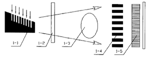
- FIG. 1 is the system schematic diagram of present invention.
- FIG. 2 is structure schematic diagram of a preferred embodiment of the interference fringes X-ray detector.
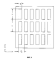
- FIG. 3 is the structure vertical view of the partial scintillator screen in the X-ray detector.
- FIG. 4 is the sectional three dimensional view of the partial scintillator screen in the X-ray detector.
- FIG. 5 is the schematic diagram of FIG. 4 after filling with X-ray sensitive material.
- FIG. 6 is the structure schematic diagram for an X-ray detector using techniques of optical fiber taper coupling.
- FIG. 1 is a systemic schematic diagram of the differential phase-contrast X-ray imaging system. Elements in the figure are represented by the numbers as follows; 1 - 1 the X-ray tube with linear arrayed structure; 1 - 2 X-ray filter, 1 - 3 object platform, 1 - 4 X-ray phase grating, 1 - 5 detector with one dimensional periodicity.
- FIG. 2 is a structure schematic diagram of a preferred embodiment of the X-ray detector composed with photon conductive material. Elements in the figure are represented by the numbers as follows; 2 - 1 glass base, 2 - 2 dielectric material, 2 - 3 the transparent electrode in the structure, 2 - 4 photoconductive material, 2 - 5 electrode. The T indicates the width of transparent electrode of 2 - 3 .
- FIG. 3 is the structure schematic diagram of partial scintillator screen in an alternative X-ray detector.
- X-ray fluorescent material is separated and forms a pixel unit array by the non-fluorescent material, the length and width of pixel unit are “a” and “b”, respectively.
- the period of the pixel unit array along X axis is P 2
- the period along Y axis is C.
- the range of C is 0.5-10 ⁇ m.
- FIG. 6 is the structure schematic diagram for an X-ray detector using techniques of optical fiber taper coupling, including 6 - 1 scintillator screen, 6 - 2 optical fiber taper, 6 - 3 array CCD or CMOS detector.
- the basic components of present system include 1 - 1 X-ray tube, 1 - 2 filter, 1 - 3 object platform, 1 - 4 X-ray phase grating, 1 - 5 detector.
- System administration software and computer control the system.
- the key factors are: 1) The coherent X-ray beam from source array whose focal spots are linearly parallel arranged, has high energy and wide angle of de angle of divergence with 30-50 degree 2)
- the novel X-ray detector adopted in present invention plays dual roles of conventional analyzer grating and conventional detector.
- the basic structure of the detector includes a set of parallel array of X-ray scintillator screen, optical coupling system, area array detector or photoconductive X-ray detector. The structure and size of the X-ray scintillator screen and the photoconductive X-ray detector are consistent with the parallel-arranged linear X-ray beam with good coherence and high energy.
- the novel X-ray tube described above is capable of generating an X-ray beam with good spatial coherence, high radiation flux, and wider emitting angles.
- a novel concept of parallel-arranged linear array of X ray emitter has been proposed by present inventor.
- the X-ray emitter is a parallel-arranged linear array consisting of many line emitters, which are considered as independent coherent sources. Proper ranges of the width and length of each line are 50-100 ⁇ m and 0.3-2 mm, and preferable are 10-20 ⁇ m and 0.6-1.2 mm respectively.
- the duty ratio of the parallel-arranged linear array of the X-ray emitter is 10-50%, the optimal ratio is 20-25%.
- each line emitter In contrast to the distance of object and source, the length of each line emitter is so small to insure the coherence of X-ray beam with shape of taper.
- Each cone of x-ray beam is individually coherent, but mutually incoherent.
- the invention of the novel X-ray tube lays the foundation for implementing the present differential phase-contrast X-ray imaging system. See CN patent 200610062487.1
- the novel X-ray tube described above can work with continuous or pulse mode.
- the X-ray tube By controlling the grid electrode located between the electronic or ionic emitter and the structured anode, the X-ray tube provides continuous or impulsive X-ray output.
- Basic components of the novel X-ray detector described above include: 6 - 1 scintillator screen, 6 - 2 light coupling system, 6 - 3 area array CCD or CMOS detector.
- the periodic structural parameters of the parallel line in the parallel-arranged linear array of X-ray scintillator screen are determined by diffraction theory.
- the loop cycle of the X-ray detector includes a banded sensitive area and a banded insensitive area. When being perpendicular to the periodic structure, the whole insensitive band, which is composed with non-fluorescent material, is insensitive to the incident X-ray. In the same direction, the whole sensitive band is divided into a rectangular array of pixels filled by x-ray fluorescent material, so every pixel is highly sensitive to the incident X-ray.
- the aggregate width of sensitive band and insensitive band is exactly same as the periodicity of the X-ray interference pattern.
- the area array detector of the X-ray detector described above is a photoconductive X-ray detector.
- the photoconductive detector is composed of independent unit made by X-ray photoconductive material. Multiple photoconductive units, which have the same structure parameters of the X-ray scintillator screen described above, are conformed together to generate an array structure.
- P 1 represents the period of phase grating
- L represents the distance from X-ray source to phase grating
- d n represents fractional Talbot imaging distance.
- the width of each independent pixel area “b” is no bigger than the one half of the period pitch (P 2 ).
- Length “a” is 0.5-10 times of period P 2 .
- non-fluorescent material such as semi-conductive material like silicon, germanium, or metal material like aluminum, or stainless steel, or glass can be selected as the non-fluorescent material described above.
- the pixel area that is separated by non-fluorescent material is filled with fluorescent material like CsI:Tl, CsI:Na or Gd 2 O 2 S:Tb that emit visible or infrared light.
- the light coupling system described above can be made of optical fiber taper, optical fiber panel, the combination of optical fiber taper and optical fiber panel, or optical lens.
- the photoconductive material is non-crystal selenium, mercury iodide, or lead iodide.
- the bases structure of the X-ray detector described above with dual functions of analyzer grating and detector is composed of 2 - 1 glass base, 2 - 2 dielectric material, 2 - 3 the transparent electrode, 2 - 4 photon conductive material, 2 - 5 electrode, wherein the photoconductive material is composed of non-crystal selenium, mercury iodide, or lead iodide.
- the “T” indicates the width of transparent electrode of 2 - 3 .
- the integrated width of 2 - 2 and 2 - 3 is equal to period length P of the grating inference fringes.
- the energy of X-ray coming from the X-ray tube adopted in present system changes from 50 to 120 keV.
- the thickness of the phase grating made of silicon, aluminum, or other material By changing the thickness of the phase grating made of silicon, aluminum, or other material, the corresponding photon energy of the central wavelength can be controlled in a range of 7-100 keV.
- the bandwidth of incident X-ray is allowed in the order of ⁇ 20% around designed center energy.
- the filter described above is made of molybdenum, tungsten, aluminum, or other material.
- the central wavelength and bandwidth of X-ray beam downstream of the filter will match the thickness of the phase grating.
- a controlling mechanism is designed to alignakily the position of the above described X-ray emitter, filter, object plate, phase grating, and X-ray detector along the coaxial or axial direction.
- a precise adjusting mechanism is designed to align extremelyly the above described X-ray source, phase grating, and array X-ray scintillator screen or photoconductive X-ray detector.
- the orientations of the parallel linear X-ray beam from the X-ray source, the direction of the phase grating line, and the one dimensional periodic structure of the X-ray array scintillator screen or photoconductive X-ray detector can be adjusted finely.
- the phase grating can also be adjusted.
- the scintillator screen structure of the first X-ray detector provided in present invention is designed as an array structure with one-dimensional period.
- the loop cycle includes banded sensitive and insensitive areas that are sensitive and insensitive to X-ray, respectively.
- the whole area of the insensitive band is insensitive to the incident X-ray, and the whole area of the sensitive band is divided into many pixels, every pixel is highly sensitive to the incident X-ray.
- the integrated width of sensitive band and insensitive band is exactly same as the periodicity of the X-ray interference pattern.
- the non-fluorescent material in the scintillator screen is semi-conductive material like silicon, germanium, or metal material like aluminum, or stainless steel, or glass.
- Array holes on the substrate are generated by etching methods like reactive ion etching, wet etching, photo-assisted electrochemical etching, or inductive coupling plasma reactive ion etching.
- the depth of the holes is usually 10-500 ⁇ m, and corresponds to the X-ray spectrum and the fluorescence material used.
- the array holes are filled with X-ray fluorescent material, which can emits visible or infrared light when being radiated by X-ray.
- multiple optical fiber tapers can be used to couple images of scintillator on the area array of CCD or CMOS detector.
- This system can be used in several fields like medical examination, non-destructive inspection, and other fields.
- the above description is only one of the preferred embodiments of the X-ray linear array of emitter, the X-ray detector with features of one dimensional spatial periodic structure, and these critical components are basis of X-ray differential interference contrast imaging system.
- X-ray source is not limited to X-ray tube using electron beam. When X-ray tube using ion beam is selected, except the ion source, other components are similar. It should be pointed out that the forms of the basic concept and basic methods of the present invention can be deduced.
Abstract
Description
Claims (2)
Applications Claiming Priority (3)
| Application Number | Priority Date | Filing Date | Title |
|---|---|---|---|
| CN200810216469 | 2008-10-10 | ||
| CN200810216469.3 | 2008-10-10 | ||
| CN2008102164693A CN101413905B (en) | 2008-10-10 | 2008-10-10 | X ray differentiation interference phase contrast imaging system |
Publications (2)
| Publication Number | Publication Date |
|---|---|
| US20100091947A1 US20100091947A1 (en) | 2010-04-15 |
| US8073099B2 true US8073099B2 (en) | 2011-12-06 |
Family
ID=40594541
Family Applications (1)
| Application Number | Title | Priority Date | Filing Date |
|---|---|---|---|
| US12/426,991 Expired - Fee Related US8073099B2 (en) | 2008-10-10 | 2009-04-21 | Differential interference phase contrast X-ray imaging system |
Country Status (2)
| Country | Link |
|---|---|
| US (1) | US8073099B2 (en) |
| CN (1) | CN101413905B (en) |
Cited By (59)
| Publication number | Priority date | Publication date | Assignee | Title |
|---|---|---|---|---|
| US20100208966A1 (en) * | 2009-02-13 | 2010-08-19 | Timothy Hughes | Method and apparatus for generating a tomographic image |
| US20120106705A1 (en) * | 2010-11-02 | 2012-05-03 | Fujifilm Corporation | Radiographic apparatus and radiographic system |
| WO2013116549A1 (en) * | 2012-02-03 | 2013-08-08 | Rapiscan Systems, Inc. | Combined scatter and transmission multi-view imaging system |
| US20130202081A1 (en) * | 2010-10-19 | 2013-08-08 | Koninklijke Philips Electronics N.V. | Differential phase-contrast imaging |
| WO2013119896A1 (en) * | 2012-02-08 | 2013-08-15 | Visuum, Llc | Multi-linear x-ray scanning systems and methods for x-ray scanning |
| US20140105353A1 (en) * | 2011-06-01 | 2014-04-17 | Universite De Pau Et Des Pays De L'adour | X-ray tomography device |
| US20140177801A1 (en) * | 2012-12-21 | 2014-06-26 | General Electric Company | Laboratory diffraction-based phase contrast imaging technique |
| US20140294148A1 (en) * | 2013-03-27 | 2014-10-02 | Siemens Aktiengesellschaft | X-ray recording system for x-ray imaging at high image frequencies of an object under examination by way of direct measurement of the interference pattern |
| US20140341347A1 (en) * | 2011-09-16 | 2014-11-20 | Siemens Aktiengesellschaft | X-ray detector of a grating-based phase contrast x-ray device and method for operating a grating-based phase contrast x-ray device |
| US20150036795A1 (en) * | 2012-01-24 | 2015-02-05 | Koninklijke Philips N.V. | Multi-directional phase contrast x-ray imaging |
| US20150241367A1 (en) * | 2012-08-30 | 2015-08-27 | Korea Atomic Energy Research Institute | Radiation imaging device capable of matter-element information acquisition and image based selection |
| US9121809B2 (en) | 2011-11-18 | 2015-09-01 | Visuum, Llc | Multi-linear X-ray scanning systems and methods for X-ray scanning |
| US20150248943A1 (en) * | 2014-03-03 | 2015-09-03 | Canon Kabushiki Kaisha | X-ray imaging system |
| US20160022235A1 (en) * | 2012-03-05 | 2016-01-28 | University Of Rochester | Methods and apparatus for differential phase-contrast cone-beam ct and hybrid cone-beam ct |
| US20160066870A1 (en) * | 2013-10-31 | 2016-03-10 | Sigray, Inc. | X-ray interferometric imaging system |
| US9513385B2 (en) | 2011-11-18 | 2016-12-06 | Visuum, Llc | Multi-linear x-ray scanning systems and methods for x-ray scanning |
| US9632206B2 (en) | 2011-09-07 | 2017-04-25 | Rapiscan Systems, Inc. | X-ray inspection system that integrates manifest data with imaging/detection processing |
| US9791590B2 (en) | 2013-01-31 | 2017-10-17 | Rapiscan Systems, Inc. | Portable security inspection system |
| US9841388B2 (en) | 2011-06-01 | 2017-12-12 | Total Sa | X-ray tomography device |
| US9880314B2 (en) | 2013-07-23 | 2018-01-30 | Rapiscan Systems, Inc. | Methods for improving processing speed for object inspection |
| US20180284298A1 (en) * | 2017-03-28 | 2018-10-04 | Konica Minolta, Inc. | Radiation conversion panel and talbot imaging device |
| US10207296B2 (en) | 2015-07-16 | 2019-02-19 | UHV Technologies, Inc. | Material sorting system |
| US10228487B2 (en) | 2014-06-30 | 2019-03-12 | American Science And Engineering, Inc. | Rapidly relocatable modular cargo container scanner |
| US10234402B2 (en) | 2017-01-05 | 2019-03-19 | Kla-Tencor Corporation | Systems and methods for defect material classification |
| US10247683B2 (en) | 2016-12-03 | 2019-04-02 | Sigray, Inc. | Material measurement techniques using multiple X-ray micro-beams |
| US10269528B2 (en) | 2013-09-19 | 2019-04-23 | Sigray, Inc. | Diverging X-ray sources using linear accumulation |
| US10297359B2 (en) | 2013-09-19 | 2019-05-21 | Sigray, Inc. | X-ray illumination system with multiple target microstructures |
| US10295485B2 (en) | 2013-12-05 | 2019-05-21 | Sigray, Inc. | X-ray transmission spectrometer system |
| US10295486B2 (en) | 2015-08-18 | 2019-05-21 | Sigray, Inc. | Detector for X-rays with high spatial and high spectral resolution |
| US10302807B2 (en) | 2016-02-22 | 2019-05-28 | Rapiscan Systems, Inc. | Systems and methods for detecting threats and contraband in cargo |
| US10304580B2 (en) | 2013-10-31 | 2019-05-28 | Sigray, Inc. | Talbot X-ray microscope |
| US10345479B2 (en) | 2015-09-16 | 2019-07-09 | Rapiscan Systems, Inc. | Portable X-ray scanner |
| US10352880B2 (en) | 2015-04-29 | 2019-07-16 | Sigray, Inc. | Method and apparatus for x-ray microscopy |
| US10401309B2 (en) | 2014-05-15 | 2019-09-03 | Sigray, Inc. | X-ray techniques using structured illumination |
| US10416099B2 (en) | 2013-09-19 | 2019-09-17 | Sigray, Inc. | Method of performing X-ray spectroscopy and X-ray absorption spectrometer system |
| US20190293573A1 (en) * | 2016-11-10 | 2019-09-26 | Koninklijke Philips N.V. | Grating-based phase contrast imaging |
| US10470721B2 (en) | 2014-11-24 | 2019-11-12 | Koninklijke Philips N.V. | Detector and imaging system for X-ray phase contrast tomo-synthesis imaging |
| US10578566B2 (en) | 2018-04-03 | 2020-03-03 | Sigray, Inc. | X-ray emission spectrometer system |
| US10600609B2 (en) | 2017-01-31 | 2020-03-24 | Rapiscan Systems, Inc. | High-power X-ray sources and methods of operation |
| US10625304B2 (en) | 2017-04-26 | 2020-04-21 | UHV Technologies, Inc. | Recycling coins from scrap |
| US10658145B2 (en) | 2018-07-26 | 2020-05-19 | Sigray, Inc. | High brightness x-ray reflection source |
| US10656105B2 (en) | 2018-08-06 | 2020-05-19 | Sigray, Inc. | Talbot-lau x-ray source and interferometric system |
| US10710119B2 (en) | 2016-07-18 | 2020-07-14 | UHV Technologies, Inc. | Material sorting using a vision system |
| US10722922B2 (en) | 2015-07-16 | 2020-07-28 | UHV Technologies, Inc. | Sorting cast and wrought aluminum |
| US10823687B2 (en) | 2015-08-03 | 2020-11-03 | UHV Technologies, Inc. | Metal analysis during pharmaceutical manufacturing |
| US10845491B2 (en) | 2018-06-04 | 2020-11-24 | Sigray, Inc. | Energy-resolving x-ray detection system |
| US10962491B2 (en) | 2018-09-04 | 2021-03-30 | Sigray, Inc. | System and method for x-ray fluorescence with filtering |
| USRE48612E1 (en) | 2013-10-31 | 2021-06-29 | Sigray, Inc. | X-ray interferometric imaging system |
| US11056308B2 (en) | 2018-09-07 | 2021-07-06 | Sigray, Inc. | System and method for depth-selectable x-ray analysis |
| US11143605B2 (en) | 2019-09-03 | 2021-10-12 | Sigray, Inc. | System and method for computed laminography x-ray fluorescence imaging |
| US11175243B1 (en) | 2020-02-06 | 2021-11-16 | Sigray, Inc. | X-ray dark-field in-line inspection for semiconductor samples |
| US11193898B1 (en) | 2020-06-01 | 2021-12-07 | American Science And Engineering, Inc. | Systems and methods for controlling image contrast in an X-ray system |
| US11212902B2 (en) | 2020-02-25 | 2021-12-28 | Rapiscan Systems, Inc. | Multiplexed drive systems and methods for a multi-emitter X-ray source |
| US11215572B2 (en) | 2020-05-18 | 2022-01-04 | Sigray, Inc. | System and method for x-ray absorption spectroscopy using a crystal analyzer and a plurality of detector elements |
| US11278937B2 (en) | 2015-07-16 | 2022-03-22 | Sortera Alloys, Inc. | Multiple stage sorting |
| US11549895B2 (en) | 2020-09-17 | 2023-01-10 | Sigray, Inc. | System and method using x-rays for depth-resolving metrology and analysis |
| US11686692B2 (en) | 2020-12-07 | 2023-06-27 | Sigray, Inc. | High throughput 3D x-ray imaging system using a transmission x-ray source |
| US11796489B2 (en) | 2021-02-23 | 2023-10-24 | Rapiscan Systems, Inc. | Systems and methods for eliminating cross-talk signals in one or more scanning systems having multiple X-ray sources |
| US11885755B2 (en) | 2022-05-02 | 2024-01-30 | Sigray, Inc. | X-ray sequential array wavelength dispersive spectrometer |
Families Citing this family (56)
| Publication number | Priority date | Publication date | Assignee | Title |
|---|---|---|---|---|
| US7949095B2 (en) * | 2009-03-02 | 2011-05-24 | University Of Rochester | Methods and apparatus for differential phase-contrast fan beam CT, cone-beam CT and hybrid cone-beam CT |
| JP5269041B2 (en) * | 2009-12-04 | 2013-08-21 | キヤノン株式会社 | X-ray imaging apparatus and X-ray imaging method |
| JP5796976B2 (en) * | 2010-05-27 | 2015-10-21 | キヤノン株式会社 | X-ray imaging device |
| CN103079469B (en) * | 2010-09-03 | 2016-02-24 | 皇家飞利浦电子股份有限公司 | Utilize differential phase contrast's imaging of the sampling improved |
| CN102353689B (en) * | 2011-06-03 | 2013-05-08 | 中国科学院上海光学精密机械研究所 | Noncoherent X ray diffraction imaging device |
| JP2013050441A (en) * | 2011-08-03 | 2013-03-14 | Canon Inc | Wavefront measuring apparatus, wavefront measuring method, program and x-ray imaging apparatus |
| WO2013030698A1 (en) * | 2011-08-31 | 2013-03-07 | Koninklijke Philips Electronics N.V. | Differential phase contrast imaging with energy sensitive detection |
| JP5920941B2 (en) | 2011-12-12 | 2016-05-18 | 株式会社日立メディコ | X-ray CT system |
| JP6177800B2 (en) * | 2012-01-12 | 2017-08-09 | コーニンクレッカ フィリップス エヌ ヴェKoninklijke Philips N.V. | Generation of attenuated image data and phase image data in an X-ray system |
| JP6076473B2 (en) | 2012-06-14 | 2017-02-08 | シーメンス アクチエンゲゼルシヤフトSiemens Aktiengesellschaft | X-ray source, use thereof and x-ray generation method |
| CN104582575B8 (en) * | 2012-08-17 | 2018-06-29 | 皇家飞利浦有限公司 | Dispose the misalignment in differential phase contrast imaging |
| US9364191B2 (en) * | 2013-02-11 | 2016-06-14 | University Of Rochester | Method and apparatus of spectral differential phase-contrast cone-beam CT and hybrid cone-beam CT |
| DE102013214393A1 (en) * | 2013-07-23 | 2014-11-20 | Siemens Aktiengesellschaft | X-ray system for differential phase-contrast imaging of an examination object with phase-stepping |
| WO2015122542A1 (en) * | 2014-02-14 | 2015-08-20 | Canon Kabushiki Kaisha | X-ray talbot interferometer and x-ray talbot interferometer system |
| CN104034741B (en) * | 2014-06-10 | 2016-10-05 | 深圳大学 | X-ray source for X-ray grating differential contrast imaging |
| EP3217879B1 (en) * | 2014-11-11 | 2020-01-08 | Koninklijke Philips N.V. | Source-detector arrangement |
| EP3265822B1 (en) | 2015-03-06 | 2021-04-28 | Micromass UK Limited | Tissue analysis by mass spectrometry or ion mobility spectrometry |
| GB2554206B (en) | 2015-03-06 | 2021-03-24 | Micromass Ltd | Spectrometric analysis of microbes |
| DE202016008460U1 (en) | 2015-03-06 | 2018-01-22 | Micromass Uk Limited | Cell population analysis |
| CN107580675B (en) | 2015-03-06 | 2020-12-08 | 英国质谱公司 | Rapid evaporative ionization mass spectrometry ("REIMS") and desorption electrospray ionization mass spectrometry ("DESI-MS") analysis of swab and biopsy samples |
| WO2016142692A1 (en) | 2015-03-06 | 2016-09-15 | Micromass Uk Limited | Spectrometric analysis |
| KR102017409B1 (en) | 2015-03-06 | 2019-10-21 | 마이크로매스 유케이 리미티드 | Improved Ionization Methods for Gaseous Samples |
| JP6858705B2 (en) | 2015-03-06 | 2021-04-14 | マイクロマス ユーケー リミテッド | Collision surface for improved ionization |
| EP3265818B1 (en) | 2015-03-06 | 2020-02-12 | Micromass UK Limited | Imaging guided ambient ionisation mass spectrometry |
| EP3265819B1 (en) | 2015-03-06 | 2020-10-14 | Micromass UK Limited | Chemically guided ambient ionisation mass spectrometry |
| CN107636794B (en) | 2015-03-06 | 2020-02-28 | 英国质谱公司 | Liquid trap or separator for electrosurgical applications |
| US10777397B2 (en) | 2015-03-06 | 2020-09-15 | Micromass Uk Limited | Inlet instrumentation for ion analyser coupled to rapid evaporative ionisation mass spectrometry (“REIMS”) device |
| US11367605B2 (en) | 2015-03-06 | 2022-06-21 | Micromass Uk Limited | Ambient ionization mass spectrometry imaging platform for direct mapping from bulk tissue |
| GB2556436B (en) | 2015-03-06 | 2022-01-26 | Micromass Ltd | Cell population analysis |
| US11139156B2 (en) | 2015-03-06 | 2021-10-05 | Micromass Uk Limited | In vivo endoscopic tissue identification tool |
| CN104833685B (en) * | 2015-04-21 | 2018-04-13 | 北京师范大学 | X-ray grating imaging system |
| GB201517195D0 (en) * | 2015-09-29 | 2015-11-11 | Micromass Ltd | Capacitively coupled reims technique and optically transparent counter electrode |
| CN105232068A (en) * | 2015-11-06 | 2016-01-13 | 深圳大学 | X-ray optical grating imaging system |
| EP3443354A1 (en) | 2016-04-14 | 2019-02-20 | Micromass UK Limited | Spectrometric analysis of plants |
| EP3469600B1 (en) | 2016-06-08 | 2019-10-02 | Koninklijke Philips N.V. | Analyzing grid for phase contrast imaging and/or dark-field imaging |
| JP6763205B2 (en) * | 2016-06-16 | 2020-09-30 | コニカミノルタ株式会社 | Laminated scintillator panel |
| JP2018146254A (en) * | 2017-03-01 | 2018-09-20 | コニカミノルタ株式会社 | Scintillator panel |
| EP3610247B1 (en) * | 2017-04-15 | 2023-08-30 | Sigray Inc. | Talbot x-ray microscope |
| US11086013B2 (en) | 2017-05-15 | 2021-08-10 | Ouster, Inc. | Micro-optics for imaging module with multiple converging lenses per channel |
| CN107621473B (en) * | 2017-08-10 | 2020-10-27 | 深圳大学 | Single X-ray differential phase contrast image detection system |
| EP3454051A1 (en) * | 2017-09-06 | 2019-03-13 | Koninklijke Philips N.V. | Diffraction grating for x-ray phase contrast and/or dark-field imaging |
| CN107703168A (en) * | 2017-10-13 | 2018-02-16 | 中国工程物理研究院材料研究所 | A kind of crystal diffraction signal acquiring method |
| EP3682229A4 (en) * | 2017-10-18 | 2021-06-09 | KA Imaging Inc. | Method and system for high-resolution x-ray detection for phase contrast x-ray imaging |
| KR102551354B1 (en) * | 2018-04-20 | 2023-07-04 | 삼성전자 주식회사 | Semiconductor light emitting devices and methods of manufacturing the same |
| CN108594344B (en) * | 2018-05-02 | 2020-06-23 | 四川大学 | Slit grating design method for weakening moire in LED naked eye 3D display |
| WO2020133531A1 (en) * | 2018-12-29 | 2020-07-02 | 深圳大学 | X-ray dual-phase grating phase-contrast imaging system |
| US11006912B2 (en) | 2019-03-25 | 2021-05-18 | Battelle Memorial Institute | Methods, systems, and computer-readable storage media for enhanced phase-contrast x-ray imaging |
| US11639903B2 (en) | 2019-03-25 | 2023-05-02 | Battelle Memorial Institute | Serial Moire scanning phase contrast x-ray imaging |
| CN111190217B (en) * | 2020-01-23 | 2022-08-02 | 中国工程物理研究院激光聚变研究中心 | Transmission band-pass type radiation flow detector |
| CN111190216B (en) * | 2020-01-23 | 2023-03-24 | 中国工程物理研究院激光聚变研究中心 | Radiation flow detector array |
| WO2021162947A1 (en) | 2020-02-10 | 2021-08-19 | Sigray, Inc. | X-ray mirror optics with multiple hyperboloidal / hyperbolic surface profiles |
| US11175245B1 (en) | 2020-06-15 | 2021-11-16 | American Science And Engineering, Inc. | Scatter X-ray imaging with adaptive scanning beam intensity |
| GB2610134A (en) * | 2020-06-15 | 2023-02-22 | American Science & Eng Inc | Scatter X-ray imaging with adaptive scanning beam intensity |
| CN112255718A (en) * | 2020-11-27 | 2021-01-22 | 深圳大学 | Large-view-field X-ray absorption grating and manufacturing method thereof |
| CN113029006B (en) * | 2021-04-27 | 2022-09-30 | 重庆理工大学 | Detection device and detection method based on moire fringes |
| CN116297578A (en) * | 2021-12-20 | 2023-06-23 | 中国科学院深圳先进技术研究院 | X-ray phase quantitative imaging technology and measuring method |
Citations (23)
| Publication number | Priority date | Publication date | Assignee | Title |
|---|---|---|---|---|
| US5354982A (en) * | 1992-07-22 | 1994-10-11 | Minnesota Mining And Manufacturing Company | Imaging system having optimized electrode geometry and processing |
| US5812629A (en) * | 1997-04-30 | 1998-09-22 | Clauser; John F. | Ultrahigh resolution interferometric x-ray imaging |
| US6078643A (en) * | 1998-05-07 | 2000-06-20 | Infimed, Inc. | Photoconductor-photocathode imager |
| US6326625B1 (en) * | 1999-01-20 | 2001-12-04 | Edge Medical Devices Ltd. | X-ray imaging system |
| US6552356B2 (en) * | 2000-03-22 | 2003-04-22 | Fuji Photo Film Co., Ltd. | Image recording medium |
| US6633627B2 (en) * | 2000-09-28 | 2003-10-14 | Ge Medical Systems Global Technology Company, Llc | X-ray CT system, gantry apparatus, console terminal, method of controlling them, and storage medium |
| CN1917135A (en) | 2006-09-07 | 2007-02-21 | 深圳大学 | New X ray tube, and fabricating method |
| WO2007074029A1 (en) * | 2005-12-27 | 2007-07-05 | Siemens Aktiengesellschaft | Focus detector arrangement for generating phase-contrast x-ray images and method for this |
| US7433444B2 (en) * | 2006-02-01 | 2008-10-07 | Siemens Aktiengesellschaft | Focus-detector arrangement of an X-ray apparatus for generating projective or tomographic phase contrast recordings |
| US7440542B2 (en) * | 2006-02-01 | 2008-10-21 | Siemens Aktiengesellschaft | Method and measuring arrangement for nondestructive analysis of an examination object by means of x-radiation |
| US7453981B2 (en) * | 2006-02-01 | 2008-11-18 | Siemens Aktiengesellschaft | Focus-detector arrangement with X-ray optical grating for phase contrast measurement |
| US7486770B2 (en) * | 2006-02-01 | 2009-02-03 | Siemens Aktiengesellschaft | Focus-detector arrangement of an X-ray apparatus for generating projective or tomographic phase contrast recordings |
| US7492871B2 (en) * | 2006-02-01 | 2009-02-17 | Siemens Aktiengesellschaft | Focus/detector system of an x-ray apparatus for generating phase contrast recordings |
| US7522708B2 (en) * | 2006-02-01 | 2009-04-21 | Siemens Aktiengesellschaft | Focus/detector system of an X-ray apparatus for generating phase contrast recordings |
| US7522698B2 (en) * | 2006-02-01 | 2009-04-21 | Siemens Aktiengesellschaft | Focus/detector system of an X-ray apparatus for generating phase contrast recordings |
| US7535986B2 (en) * | 2006-02-01 | 2009-05-19 | Siemens Aktiengesellschaft | Method and CT system for detecting and differentiating plaque in vessel structures of a patient |
| US7564941B2 (en) * | 2006-02-01 | 2009-07-21 | Siemens Aktiengesellschaft | Focus-detector arrangement for generating projective or tomographic phase contrast recordings with X-ray optical gratings |
| US7639786B2 (en) * | 2006-02-01 | 2009-12-29 | Siemens Aktiengesellschaft | X-ray optical transmission grating of a focus-detector arrangement of an X-ray apparatus for generating projective or tomographic phase contrast recordings of a subject |
| US7646843B2 (en) * | 2006-02-01 | 2010-01-12 | Siemens Aktiengesellschaft | Method for producing projective and tomographic phase contrast images with the aid of an X-ray system |
| US7746981B2 (en) * | 2007-10-31 | 2010-06-29 | Fujifilm Corporation | Radiation image detector and phase contrast radiation imaging apparatus |
| US7817777B2 (en) * | 2005-12-27 | 2010-10-19 | Siemens Aktiengesellschaft | Focus detector arrangement and method for generating contrast x-ray images |
| US7889838B2 (en) * | 2005-06-06 | 2011-02-15 | Paul Scherrer Institut | Interferometer for quantitative phase contrast imaging and tomography with an incoherent polychromatic x-ray source |
| US7924973B2 (en) * | 2007-11-15 | 2011-04-12 | Csem Centre Suisse D'electronique Et De Microtechnique Sa | Interferometer device and method |
Family Cites Families (1)
| Publication number | Priority date | Publication date | Assignee | Title |
|---|---|---|---|---|
| DE10151568A1 (en) * | 2001-10-23 | 2003-05-08 | Siemens Ag | Method for applying an anti-scatter grid to an X-ray detector |
-
2008
- 2008-10-10 CN CN2008102164693A patent/CN101413905B/en not_active Expired - Fee Related
-
2009
- 2009-04-21 US US12/426,991 patent/US8073099B2/en not_active Expired - Fee Related
Patent Citations (23)
| Publication number | Priority date | Publication date | Assignee | Title |
|---|---|---|---|---|
| US5354982A (en) * | 1992-07-22 | 1994-10-11 | Minnesota Mining And Manufacturing Company | Imaging system having optimized electrode geometry and processing |
| US5812629A (en) * | 1997-04-30 | 1998-09-22 | Clauser; John F. | Ultrahigh resolution interferometric x-ray imaging |
| US6078643A (en) * | 1998-05-07 | 2000-06-20 | Infimed, Inc. | Photoconductor-photocathode imager |
| US6326625B1 (en) * | 1999-01-20 | 2001-12-04 | Edge Medical Devices Ltd. | X-ray imaging system |
| US6552356B2 (en) * | 2000-03-22 | 2003-04-22 | Fuji Photo Film Co., Ltd. | Image recording medium |
| US6633627B2 (en) * | 2000-09-28 | 2003-10-14 | Ge Medical Systems Global Technology Company, Llc | X-ray CT system, gantry apparatus, console terminal, method of controlling them, and storage medium |
| US7889838B2 (en) * | 2005-06-06 | 2011-02-15 | Paul Scherrer Institut | Interferometer for quantitative phase contrast imaging and tomography with an incoherent polychromatic x-ray source |
| WO2007074029A1 (en) * | 2005-12-27 | 2007-07-05 | Siemens Aktiengesellschaft | Focus detector arrangement for generating phase-contrast x-ray images and method for this |
| US7817777B2 (en) * | 2005-12-27 | 2010-10-19 | Siemens Aktiengesellschaft | Focus detector arrangement and method for generating contrast x-ray images |
| US7453981B2 (en) * | 2006-02-01 | 2008-11-18 | Siemens Aktiengesellschaft | Focus-detector arrangement with X-ray optical grating for phase contrast measurement |
| US7564941B2 (en) * | 2006-02-01 | 2009-07-21 | Siemens Aktiengesellschaft | Focus-detector arrangement for generating projective or tomographic phase contrast recordings with X-ray optical gratings |
| US7486770B2 (en) * | 2006-02-01 | 2009-02-03 | Siemens Aktiengesellschaft | Focus-detector arrangement of an X-ray apparatus for generating projective or tomographic phase contrast recordings |
| US7492871B2 (en) * | 2006-02-01 | 2009-02-17 | Siemens Aktiengesellschaft | Focus/detector system of an x-ray apparatus for generating phase contrast recordings |
| US7522708B2 (en) * | 2006-02-01 | 2009-04-21 | Siemens Aktiengesellschaft | Focus/detector system of an X-ray apparatus for generating phase contrast recordings |
| US7522698B2 (en) * | 2006-02-01 | 2009-04-21 | Siemens Aktiengesellschaft | Focus/detector system of an X-ray apparatus for generating phase contrast recordings |
| US7535986B2 (en) * | 2006-02-01 | 2009-05-19 | Siemens Aktiengesellschaft | Method and CT system for detecting and differentiating plaque in vessel structures of a patient |
| US7440542B2 (en) * | 2006-02-01 | 2008-10-21 | Siemens Aktiengesellschaft | Method and measuring arrangement for nondestructive analysis of an examination object by means of x-radiation |
| US7639786B2 (en) * | 2006-02-01 | 2009-12-29 | Siemens Aktiengesellschaft | X-ray optical transmission grating of a focus-detector arrangement of an X-ray apparatus for generating projective or tomographic phase contrast recordings of a subject |
| US7646843B2 (en) * | 2006-02-01 | 2010-01-12 | Siemens Aktiengesellschaft | Method for producing projective and tomographic phase contrast images with the aid of an X-ray system |
| US7433444B2 (en) * | 2006-02-01 | 2008-10-07 | Siemens Aktiengesellschaft | Focus-detector arrangement of an X-ray apparatus for generating projective or tomographic phase contrast recordings |
| CN1917135A (en) | 2006-09-07 | 2007-02-21 | 深圳大学 | New X ray tube, and fabricating method |
| US7746981B2 (en) * | 2007-10-31 | 2010-06-29 | Fujifilm Corporation | Radiation image detector and phase contrast radiation imaging apparatus |
| US7924973B2 (en) * | 2007-11-15 | 2011-04-12 | Csem Centre Suisse D'electronique Et De Microtechnique Sa | Interferometer device and method |
Non-Patent Citations (1)
| Title |
|---|
| Engelhardt, et. al, High-Resolution Differential Phase Contrast Imaging Using Microfocus X-ray Sources, International Sumposium on Digital industrial Radiology, 2007, France. |
Cited By (95)
| Publication number | Priority date | Publication date | Assignee | Title |
|---|---|---|---|---|
| US9662036B2 (en) * | 2009-02-13 | 2017-05-30 | Siemens Aktiengesellschaft | Method and apparatus for generating a tomographic image |
| US20100208966A1 (en) * | 2009-02-13 | 2010-08-19 | Timothy Hughes | Method and apparatus for generating a tomographic image |
| US9861330B2 (en) * | 2010-10-19 | 2018-01-09 | Koninklijke Philips N.V. | Differential phase-contrast imaging |
| US20130202081A1 (en) * | 2010-10-19 | 2013-08-08 | Koninklijke Philips Electronics N.V. | Differential phase-contrast imaging |
| US20120106705A1 (en) * | 2010-11-02 | 2012-05-03 | Fujifilm Corporation | Radiographic apparatus and radiographic system |
| US9557280B2 (en) * | 2011-06-01 | 2017-01-31 | Total Sa | X-ray tomography device |
| US20140105353A1 (en) * | 2011-06-01 | 2014-04-17 | Universite De Pau Et Des Pays De L'adour | X-ray tomography device |
| US9841388B2 (en) | 2011-06-01 | 2017-12-12 | Total Sa | X-ray tomography device |
| US10830920B2 (en) | 2011-09-07 | 2020-11-10 | Rapiscan Systems, Inc. | Distributed analysis X-ray inspection methods and systems |
| US11099294B2 (en) | 2011-09-07 | 2021-08-24 | Rapiscan Systems, Inc. | Distributed analysis x-ray inspection methods and systems |
| US10509142B2 (en) | 2011-09-07 | 2019-12-17 | Rapiscan Systems, Inc. | Distributed analysis x-ray inspection methods and systems |
| US9632206B2 (en) | 2011-09-07 | 2017-04-25 | Rapiscan Systems, Inc. | X-ray inspection system that integrates manifest data with imaging/detection processing |
| US10422919B2 (en) | 2011-09-07 | 2019-09-24 | Rapiscan Systems, Inc. | X-ray inspection system that integrates manifest data with imaging/detection processing |
| US20140341347A1 (en) * | 2011-09-16 | 2014-11-20 | Siemens Aktiengesellschaft | X-ray detector of a grating-based phase contrast x-ray device and method for operating a grating-based phase contrast x-ray device |
| US9402594B2 (en) * | 2011-09-16 | 2016-08-02 | Siemens Aktiengesellschaft | X-ray detector of a grating-based phase contrast x-ray device and method for operating a grating-based phase contrast x-ray device |
| US8989348B2 (en) | 2011-11-18 | 2015-03-24 | Visuum, Llc | Multi-linear X-ray scanning systems and methods for X-ray scanning |
| US9513385B2 (en) | 2011-11-18 | 2016-12-06 | Visuum, Llc | Multi-linear x-ray scanning systems and methods for x-ray scanning |
| US9689811B2 (en) | 2011-11-18 | 2017-06-27 | Visuum, Llc | Multi-linear X-ray scanning systems and methods for X-ray scanning |
| US9121809B2 (en) | 2011-11-18 | 2015-09-01 | Visuum, Llc | Multi-linear X-ray scanning systems and methods for X-ray scanning |
| US20150036795A1 (en) * | 2012-01-24 | 2015-02-05 | Koninklijke Philips N.V. | Multi-directional phase contrast x-ray imaging |
| US9597050B2 (en) * | 2012-01-24 | 2017-03-21 | Koninklijke Philips N.V. | Multi-directional phase contrast X-ray imaging |
| US10746674B2 (en) | 2012-02-03 | 2020-08-18 | Rapiscan Systems, Inc. | Combined scatter and transmission multi-view imaging system |
| US9823201B2 (en) | 2012-02-03 | 2017-11-21 | Rapiscan Systems, Inc. | Combined scatter and transmission multi-view imaging system |
| GB2513073B (en) * | 2012-02-03 | 2018-03-21 | Rapiscan Systems Inc | Combined scatter and transmission multi-view imaging system |
| US9057679B2 (en) | 2012-02-03 | 2015-06-16 | Rapiscan Systems, Inc. | Combined scatter and transmission multi-view imaging system |
| US11371948B2 (en) | 2012-02-03 | 2022-06-28 | Rapiscan Systems, Inc. | Multi-view imaging system |
| GB2513073A (en) * | 2012-02-03 | 2014-10-15 | Rapiscan Systems Inc | Combined scatter and transmission multi-view imaging system |
| WO2013116549A1 (en) * | 2012-02-03 | 2013-08-08 | Rapiscan Systems, Inc. | Combined scatter and transmission multi-view imaging system |
| WO2013119896A1 (en) * | 2012-02-08 | 2013-08-15 | Visuum, Llc | Multi-linear x-ray scanning systems and methods for x-ray scanning |
| US9826949B2 (en) * | 2012-03-05 | 2017-11-28 | University Of Rochester | Methods and apparatus for differential phase-contrast cone-beam CT and hybrid cone-beam CT |
| US20160022235A1 (en) * | 2012-03-05 | 2016-01-28 | University Of Rochester | Methods and apparatus for differential phase-contrast cone-beam ct and hybrid cone-beam ct |
| US9784697B2 (en) * | 2012-08-30 | 2017-10-10 | Korea Atomic Energy Research Institute | Radiation imaging device capable of matter-element information acquisition and image based selection |
| US20150241367A1 (en) * | 2012-08-30 | 2015-08-27 | Korea Atomic Energy Research Institute | Radiation imaging device capable of matter-element information acquisition and image based selection |
| US9068927B2 (en) * | 2012-12-21 | 2015-06-30 | General Electric Company | Laboratory diffraction-based phase contrast imaging technique |
| US20140177801A1 (en) * | 2012-12-21 | 2014-06-26 | General Electric Company | Laboratory diffraction-based phase contrast imaging technique |
| US9791590B2 (en) | 2013-01-31 | 2017-10-17 | Rapiscan Systems, Inc. | Portable security inspection system |
| US11550077B2 (en) | 2013-01-31 | 2023-01-10 | Rapiscan Systems, Inc. | Portable vehicle inspection portal with accompanying workstation |
| US10317566B2 (en) | 2013-01-31 | 2019-06-11 | Rapiscan Systems, Inc. | Portable security inspection system |
| US20140294148A1 (en) * | 2013-03-27 | 2014-10-02 | Siemens Aktiengesellschaft | X-ray recording system for x-ray imaging at high image frequencies of an object under examination by way of direct measurement of the interference pattern |
| US9414796B2 (en) * | 2013-03-27 | 2016-08-16 | Siemens Aktiengesellschaft | X-ray recording system for x-ray imaging at high image frequencies of an object under examination by way of direct measurement of the interference pattern |
| US9880314B2 (en) | 2013-07-23 | 2018-01-30 | Rapiscan Systems, Inc. | Methods for improving processing speed for object inspection |
| US10297359B2 (en) | 2013-09-19 | 2019-05-21 | Sigray, Inc. | X-ray illumination system with multiple target microstructures |
| US10269528B2 (en) | 2013-09-19 | 2019-04-23 | Sigray, Inc. | Diverging X-ray sources using linear accumulation |
| US10416099B2 (en) | 2013-09-19 | 2019-09-17 | Sigray, Inc. | Method of performing X-ray spectroscopy and X-ray absorption spectrometer system |
| US10976273B2 (en) | 2013-09-19 | 2021-04-13 | Sigray, Inc. | X-ray spectrometer system |
| US10304580B2 (en) | 2013-10-31 | 2019-05-28 | Sigray, Inc. | Talbot X-ray microscope |
| USRE48612E1 (en) | 2013-10-31 | 2021-06-29 | Sigray, Inc. | X-ray interferometric imaging system |
| US10653376B2 (en) | 2013-10-31 | 2020-05-19 | Sigray, Inc. | X-ray imaging system |
| US10349908B2 (en) * | 2013-10-31 | 2019-07-16 | Sigray, Inc. | X-ray interferometric imaging system |
| US20160066870A1 (en) * | 2013-10-31 | 2016-03-10 | Sigray, Inc. | X-ray interferometric imaging system |
| US10295485B2 (en) | 2013-12-05 | 2019-05-21 | Sigray, Inc. | X-ray transmission spectrometer system |
| US20150248943A1 (en) * | 2014-03-03 | 2015-09-03 | Canon Kabushiki Kaisha | X-ray imaging system |
| US10401309B2 (en) | 2014-05-15 | 2019-09-03 | Sigray, Inc. | X-ray techniques using structured illumination |
| US10228487B2 (en) | 2014-06-30 | 2019-03-12 | American Science And Engineering, Inc. | Rapidly relocatable modular cargo container scanner |
| US10470721B2 (en) | 2014-11-24 | 2019-11-12 | Koninklijke Philips N.V. | Detector and imaging system for X-ray phase contrast tomo-synthesis imaging |
| US10352880B2 (en) | 2015-04-29 | 2019-07-16 | Sigray, Inc. | Method and apparatus for x-ray microscopy |
| US11278937B2 (en) | 2015-07-16 | 2022-03-22 | Sortera Alloys, Inc. | Multiple stage sorting |
| US10207296B2 (en) | 2015-07-16 | 2019-02-19 | UHV Technologies, Inc. | Material sorting system |
| US10722922B2 (en) | 2015-07-16 | 2020-07-28 | UHV Technologies, Inc. | Sorting cast and wrought aluminum |
| US11471916B2 (en) | 2015-07-16 | 2022-10-18 | Sortera Alloys, Inc. | Metal sorter |
| US10823687B2 (en) | 2015-08-03 | 2020-11-03 | UHV Technologies, Inc. | Metal analysis during pharmaceutical manufacturing |
| US10295486B2 (en) | 2015-08-18 | 2019-05-21 | Sigray, Inc. | Detector for X-rays with high spatial and high spectral resolution |
| US10345479B2 (en) | 2015-09-16 | 2019-07-09 | Rapiscan Systems, Inc. | Portable X-ray scanner |
| US10302807B2 (en) | 2016-02-22 | 2019-05-28 | Rapiscan Systems, Inc. | Systems and methods for detecting threats and contraband in cargo |
| US11287391B2 (en) | 2016-02-22 | 2022-03-29 | Rapiscan Systems, Inc. | Systems and methods for detecting threats and contraband in cargo |
| US10768338B2 (en) | 2016-02-22 | 2020-09-08 | Rapiscan Systems, Inc. | Systems and methods for detecting threats and contraband in cargo |
| US10710119B2 (en) | 2016-07-18 | 2020-07-14 | UHV Technologies, Inc. | Material sorting using a vision system |
| US11000249B2 (en) * | 2016-11-10 | 2021-05-11 | Koninklijke Philips N.V. | X-ray detector for grating-based phase-contrast imaging |
| US20190293573A1 (en) * | 2016-11-10 | 2019-09-26 | Koninklijke Philips N.V. | Grating-based phase contrast imaging |
| US10247683B2 (en) | 2016-12-03 | 2019-04-02 | Sigray, Inc. | Material measurement techniques using multiple X-ray micro-beams |
| US10466185B2 (en) | 2016-12-03 | 2019-11-05 | Sigray, Inc. | X-ray interrogation system using multiple x-ray beams |
| US10234402B2 (en) | 2017-01-05 | 2019-03-19 | Kla-Tencor Corporation | Systems and methods for defect material classification |
| US10670537B2 (en) | 2017-01-05 | 2020-06-02 | Kla-Tencor Corporation | Systems and methods for defect material classification |
| US10600609B2 (en) | 2017-01-31 | 2020-03-24 | Rapiscan Systems, Inc. | High-power X-ray sources and methods of operation |
| US20180284298A1 (en) * | 2017-03-28 | 2018-10-04 | Konica Minolta, Inc. | Radiation conversion panel and talbot imaging device |
| US10625304B2 (en) | 2017-04-26 | 2020-04-21 | UHV Technologies, Inc. | Recycling coins from scrap |
| US11260426B2 (en) | 2017-04-26 | 2022-03-01 | Sortera Alloys, hic. | Identifying coins from scrap |
| US10578566B2 (en) | 2018-04-03 | 2020-03-03 | Sigray, Inc. | X-ray emission spectrometer system |
| US10845491B2 (en) | 2018-06-04 | 2020-11-24 | Sigray, Inc. | Energy-resolving x-ray detection system |
| US10989822B2 (en) | 2018-06-04 | 2021-04-27 | Sigray, Inc. | Wavelength dispersive x-ray spectrometer |
| US10658145B2 (en) | 2018-07-26 | 2020-05-19 | Sigray, Inc. | High brightness x-ray reflection source |
| US10991538B2 (en) | 2018-07-26 | 2021-04-27 | Sigray, Inc. | High brightness x-ray reflection source |
| US10656105B2 (en) | 2018-08-06 | 2020-05-19 | Sigray, Inc. | Talbot-lau x-ray source and interferometric system |
| US10962491B2 (en) | 2018-09-04 | 2021-03-30 | Sigray, Inc. | System and method for x-ray fluorescence with filtering |
| US11056308B2 (en) | 2018-09-07 | 2021-07-06 | Sigray, Inc. | System and method for depth-selectable x-ray analysis |
| US11143605B2 (en) | 2019-09-03 | 2021-10-12 | Sigray, Inc. | System and method for computed laminography x-ray fluorescence imaging |
| US11175243B1 (en) | 2020-02-06 | 2021-11-16 | Sigray, Inc. | X-ray dark-field in-line inspection for semiconductor samples |
| US11212902B2 (en) | 2020-02-25 | 2021-12-28 | Rapiscan Systems, Inc. | Multiplexed drive systems and methods for a multi-emitter X-ray source |
| US11215572B2 (en) | 2020-05-18 | 2022-01-04 | Sigray, Inc. | System and method for x-ray absorption spectroscopy using a crystal analyzer and a plurality of detector elements |
| US11428651B2 (en) | 2020-05-18 | 2022-08-30 | Sigray, Inc. | System and method for x-ray absorption spectroscopy using a crystal analyzer and a plurality of detector elements |
| US11193898B1 (en) | 2020-06-01 | 2021-12-07 | American Science And Engineering, Inc. | Systems and methods for controlling image contrast in an X-ray system |
| US11549895B2 (en) | 2020-09-17 | 2023-01-10 | Sigray, Inc. | System and method using x-rays for depth-resolving metrology and analysis |
| US11686692B2 (en) | 2020-12-07 | 2023-06-27 | Sigray, Inc. | High throughput 3D x-ray imaging system using a transmission x-ray source |
| US11796489B2 (en) | 2021-02-23 | 2023-10-24 | Rapiscan Systems, Inc. | Systems and methods for eliminating cross-talk signals in one or more scanning systems having multiple X-ray sources |
| US11885755B2 (en) | 2022-05-02 | 2024-01-30 | Sigray, Inc. | X-ray sequential array wavelength dispersive spectrometer |
Also Published As
| Publication number | Publication date |
|---|---|
| CN101413905A (en) | 2009-04-22 |
| CN101413905B (en) | 2011-03-16 |
| US20100091947A1 (en) | 2010-04-15 |
Similar Documents
| Publication | Publication Date | Title |
|---|---|---|
| US8073099B2 (en) | Differential interference phase contrast X-ray imaging system | |
| JP6775035B2 (en) | Methods and equipment for X-ray microscopy | |
| US20150055745A1 (en) | Phase Contrast Imaging Using Patterned Illumination/Detector and Phase Mask | |
| US7342996B2 (en) | X-ray means for determining the location of malignant neoplasm and its radiotherapy | |
| US7583789B1 (en) | X-ray imaging systems employing point-focusing, curved monochromating optics | |
| CN1041237C (en) | X-ray detector for a low dosage scanning beam digital X-ray imaging system | |
| EP0061496B1 (en) | X-ray intensifier detector system for x-ray electronic radiography | |
| US20180261350A1 (en) | Talbot x-ray microscope | |
| Tommasini et al. | Short pulse, high resolution, backlighters for point projection high-energy radiography at the National Ignition Facility | |
| CN111166363A (en) | X-ray interference imaging system | |
| EP1188165A1 (en) | Parallel x-ray nanotomography | |
| JPS58118733A (en) | Radiography apparatus | |
| JP2008268105A (en) | X-ray beam source, x-ray beam irradiator, x-ray beam radiographic device, x-ray beam computer tomography device, x-ray element mapping examination apparatus and x-ray beam forming method | |
| JP7252938B2 (en) | Focused X-ray Imaging Apparatus and Method | |
| US11000249B2 (en) | X-ray detector for grating-based phase-contrast imaging | |
| JP7066739B2 (en) | Talbot X-ray microscope | |
| RU2164081C2 (en) | Limited-angle x-ray tomograph | |
| JPS62106352A (en) | Scanning type x-ray microscope | |
| JP4623879B2 (en) | Beam evaluation method and apparatus | |
| Portillo et al. | Time-resolved spot size measurements from various radiographic diodes on the RITS-3 accelerator | |
| Kumakhov | State and perspectives of capillary Roentgen optics | |
| Tsipenyuk | Poly-capillary X-ray and neutron optics (Kumakhov optics) | |
| CN110520716A (en) | TALBOT X-ray microscope | |
| GB2133611A (en) | Radiographic magnifying device | |
| Rich | Laser etch monitoring system |
Legal Events
| Date | Code | Title | Description |
|---|---|---|---|
| AS | Assignment |
Owner name: SHENZHEN UNIVERSITY,CHINA Free format text: ASSIGNMENT OF ASSIGNORS INTEREST;ASSIGNORS:NIU, HAN-BEN;GUO, JIN-CHUAN;LIU, XIN;REEL/FRAME:022811/0127 Effective date: 20090521 Owner name: SHENZHEN UNIVERSITY, CHINA Free format text: ASSIGNMENT OF ASSIGNORS INTEREST;ASSIGNORS:NIU, HAN-BEN;GUO, JIN-CHUAN;LIU, XIN;REEL/FRAME:022811/0127 Effective date: 20090521 |
|
| FEPP | Fee payment procedure |
Free format text: PAYOR NUMBER ASSIGNED (ORIGINAL EVENT CODE: ASPN); ENTITY STATUS OF PATENT OWNER: SMALL ENTITY |
|
| STCF | Information on status: patent grant |
Free format text: PATENTED CASE |
|
| FEPP | Fee payment procedure |
Free format text: PAYER NUMBER DE-ASSIGNED (ORIGINAL EVENT CODE: RMPN); ENTITY STATUS OF PATENT OWNER: SMALL ENTITY Free format text: PAYOR NUMBER ASSIGNED (ORIGINAL EVENT CODE: ASPN); ENTITY STATUS OF PATENT OWNER: SMALL ENTITY |
|
| REMI | Maintenance fee reminder mailed | ||
| FPAY | Fee payment |
Year of fee payment: 4 |
|
| SULP | Surcharge for late payment | ||
| FEPP | Fee payment procedure |
Free format text: MAINTENANCE FEE REMINDER MAILED (ORIGINAL EVENT CODE: REM.); ENTITY STATUS OF PATENT OWNER: SMALL ENTITY |
|
| LAPS | Lapse for failure to pay maintenance fees |
Free format text: PATENT EXPIRED FOR FAILURE TO PAY MAINTENANCE FEES (ORIGINAL EVENT CODE: EXP.); ENTITY STATUS OF PATENT OWNER: SMALL ENTITY |
|
| STCH | Information on status: patent discontinuation |
Free format text: PATENT EXPIRED DUE TO NONPAYMENT OF MAINTENANCE FEES UNDER 37 CFR 1.362 |
|
| FP | Lapsed due to failure to pay maintenance fee |
Effective date: 20191206 |