US7436449B2 - Electronic imaging system - Google Patents
Electronic imaging system Download PDFInfo
- Publication number
- US7436449B2 US7436449B2 US10/618,675 US61867503A US7436449B2 US 7436449 B2 US7436449 B2 US 7436449B2 US 61867503 A US61867503 A US 61867503A US 7436449 B2 US7436449 B2 US 7436449B2
- Authority
- US
- United States
- Prior art keywords
- image pickup
- pickup device
- electronic
- zoom lens
- electronic image
- Prior art date
- Legal status (The legal status is an assumption and is not a legal conclusion. Google has not performed a legal analysis and makes no representation as to the accuracy of the status listed.)
- Expired - Fee Related, expires
Links
Images


Classifications
-
- G—PHYSICS
- G02—OPTICS
- G02B—OPTICAL ELEMENTS, SYSTEMS OR APPARATUS
- G02B15/00—Optical objectives with means for varying the magnification
- G02B15/14—Optical objectives with means for varying the magnification by axial movement of one or more lenses or groups of lenses relative to the image plane for continuously varying the equivalent focal length of the objective
- G02B15/144—Optical objectives with means for varying the magnification by axial movement of one or more lenses or groups of lenses relative to the image plane for continuously varying the equivalent focal length of the objective having four groups only
- G02B15/1445—Optical objectives with means for varying the magnification by axial movement of one or more lenses or groups of lenses relative to the image plane for continuously varying the equivalent focal length of the objective having four groups only the first group being negative
Definitions
- the primary object of the present invention is to provide the technology for implementing video or digital cameras whose depth dimension is reduced while high image quality is ensured, and which are easy to handle.
- the gravest bottleneck in diminishing the depth dimension of cameras is the thickness of an optical system, especially a zoom lens system from the surface located nearest to its object side to an image pickup plane.
- Recent technologies for slimming down cameras rely primarily on a collapsible lens mount that allows the optical system to be taken out of a camera body for phototaking and received therein for carrying.
- Typical examples of the zoom lens system so far known to be well fit for electronic image pickup devices and have satisfactory image-formation performance inclusive of zoom ratio, angle of view and F-number are disclosed in JP-A's 11-287953, 2000-267009 and 2000-275520.
- an electronic imaging system comprising a zoom lens system and an electronic image pickup device located on its image side so that the image of a subject can be formed on the photoreceptive surface of the electronic image pickup device for conversion into electric signals, wherein:
- an electronic imaging system comprising a zoom lens system and an electronic image pickup device located on its image side so that the image of a subject can be formed on the photoreceptive surface of the electronic image pickup device for conversion into electric signals, wherein:
- a so-called optical low-pass filter is located between a subject and an image pickup device and on the optical path of an optical system, so that a subject image formed by a lens is displaced roughly by a pixel pitch using the double-refraction action of a uniaxial crystal such as rock crystal into a double image, thereby reducing contrast in the vicinity of the Nyquist frequency component.
- the resolution limit of an image pickup device having a plurality of pixels is given by 1 ⁇ 2a where a is the horizontal pixel pitch.
- a is the horizontal pixel pitch.
- the maximum F-number upon stopping-down is defined by (maximum F-number at the wide-angle end+maximum F-number at the telephoto end)/2 This value is hereinafter called F′. It is then preferable to satisfy 2.0 ⁇ 10 3 ⁇ a/ 1 mm ⁇ F′ ⁇ 4.5 ⁇ 10 3 ⁇ a/ 1 mm (3)
- the aperture shape of the stop should preferably be limited to two types, i.e., a full aperture state and a state where the F-number (F′) satisfying the aforesaid condition is obtained.
- the ratio between the maximum F-number and the minimum F-number should be in the range of 1.4 to 3 inclusive.
- lens surfaces adjacent to the aperture stop are configured in such a way that at least one thereof is convex toward the aperture stop and another passes through the aperture stop, further size reductions are then achievable because any extra space taken up by the aperture stop is completely eliminated.
- the mode of reading signals from the image pickup device has a sequential reading function.
- the sequential reading of signals should preferably be performed using only one of odd-number fields or even-number fields.
- signals at the n line and n+1 line at a certain row should be read in a mixed fashion.
- control of light quantity is preferably performed by control of shutter speed.
- the interlaced scanning mode is favorable for practical image pickup devices with an increasing number of pixels, and so a mechanical shutter is used in such a way that two fields, i.e., an odd-number field and an even-number field are simultaneously phototaken and signals are separately read.
- the mechanical shutter cannot be used for extremely bright subjects. It is thus preferable to make use of a method for using only one field or mixing two fields together for phototaking and reading, although there is a drop of vertical resolution. According to this method, it is unnecessary to read both the odd-number and even-number fields separately, i.e., use the mechanical shutter. In other words, it is possible to use a shutter that enables the potential of an image pickup device to be controlled at a very fast speed (hereinafter called a device shutter), thereby achieving a shutter speed faster than 1/10,000 second.
- a device shutter a very fast speed
- the zoom lens system of the present invention comprises, in order from its object side, a lens group Ax having negative refracting power and a lens group Bx having positive refracting power, and consists of up to 5 lenses in all.
- the lens groups Ax and Bx move.
- the lens group Bx should preferably consist of up to two lens components (provided that a cemented lens is counted as one component). More preferably, the zoom lens system should consist of only two movable lens groups, i.e., the lens group Ax having negative refracting power and the lens group Bx having positive refracting power.
- an infrared absorption filter having a certain thickness is usually inserted between an image pickup device and the object side of a zoom lens, so that the incidence of infrared light on the image pickup plane is prevented.
- this filter is replaced by a coating devoid of thickness so as to reduce the length and thickness of the optical system.
- this filter is replaced by a coating devoid of thickness so as to reduce the length and thickness of the optical system.
- Another defect of the CCD or other solid-state image pickup device is that the sensitivity to the wavelength of 550 nm in the near ultraviolet range is considerably higher than that of the human eye. This, too, makes noticeable chromatic blurring at the edges of an image due to chromatic aberrations in the near-ultraviolet range. Such color blurring is fatal to a compact optical system.
- an absorber or reflector is inserted onto the optical path, which is designed such that the ratio of the transmittance ( ⁇ 400 ) at 400 nm wavelength to that ( ⁇ 550 ) at 550 nm wavelength is less than 0.08 and the ratio of the transmittance ( ⁇ 440 ) at 440 nm wavelength to that ( ⁇ 550 ) at 550 nm wavelength is greater than 0.4, it is then possible to considerably reduce noises such as chromatic blurring while the wavelength range necessary for color reproduction (satisfactory color reproduction) is kept intact.
- condition (9)′′ and (10)′′ should be satisfied.
- these filters should preferably be located between the image-formation optical system and the image pickup device.
- a complementary colors filter is higher in substantial sensitivity and more favorable in resolution than a primary colors filter-inserted CCD due to its high transmitted light energy, and provides a great merit when used in combination with a small-size CCD. It is also desirable to locate an optical element having a transmittance of up to 90% (where possible, the entrance and exit surfaces of the optical element should preferably be defined by planar surfaces) in a space including the optical axis at least one lens away from the aperture stop or use means for replacing that optical element by another element having a different transmittance.
- the electronic imaging system is designed in such a way as to have a plurality of apertures each of fixed aperture size, one of which can be inserted into any one of optical paths between the lens surface located nearest to the image side of the first lens group and the lens surface located nearest to the object side of the third lens group and can be replaced with another as well, so that the illuminance on the image plane can be adjusted. Then, media whose transmittances with respect to 550 nm are different but less than 80% are filled in some of the plurality of apertures for light quantity control.
- any medium is not used or dummy media having a transmittance of at least 91% with respect to 550 nm are used.
- the medium on the optical path between the zoom lens system and the electronic image pickup device is all composed only of air or a non-crystalline medium showing anisotropy.
- glasses or plastics may be used.
- FIGS. 1( a ), 1 ( b ) and 1 ( c ) are illustrative in section of Example 1 of the zoom lens according to the invention at the wide-angle end (a), in an intermediate state (b) and at the telephoto end (c), respectively, when the zoom lens is focused on an object point at infinity.
- FIG. 2 is illustrative in section of Example 1 of the zoom lens of the invention upon bending at the wide-angle end when the zoom lens is focused on an infinite object point.
- FIGS. 3( a ), 3 ( b ) and 3 ( c ) are aberration diagrams for Example 1 when it is focused on an infinite object point.
- FIG. 4 is illustrative of horizontal wave optics MTF characteristics at a central area of the screen upon a full aperture at the wide-angle end.
- FIG. 5 is illustrative of horizontal wave optics MTF characteristics at a central area of the screen upon a full aperture at an intermediate distance.
- FIG. 6 is illustrative of horizontal wave optics MTF characteristics at a central area of the screen upon a full aperture at the telephoto end.
- FIG. 7 is illustrative of horizontal wave optics MTF characteristics at a central area of the screen upon a two-stop aperture at the wide-angle end.
- FIG. 8 is illustrative of horizontal wave optics MTF characteristics at a central area of the screen upon a two-stop aperture at an intermediate distance.
- FIG. 9 is illustrative of horizontal wave optics MTF characteristics at a central area of the screen upon a two-stop aperture at the telephoto end.
- FIG. 10 is a characteristic diagram for an example where the horizontal wave optics MTF is high.
- FIG. 11 is illustrative of the stop whose aperture shape is in a full-aperture state.
- FIG. 12 is illustrative of the stop whose aperture shape is in a two-stop state.
- FIG. 13 is illustrative of the diagonal length of the effective image pickup plane of an electronic image pickup device upon phototaking.
- FIG. 14 is a diagram indicative of the transmittance characteristics of one example of the near-infrared sharp cut coat.
- FIG. 15 is a schematic illustrative of how the color filter elements are arranged in the complementary colors mosaic filter.
- FIG. 16 is a diagram indicative of one example of the wavelength characteristics of the complementary colors mosaic filter.
- FIG. 17 is a perspective view of details of one example of the aperture stop portion used in the example.
- FIG. 18 is illustrative in detail of another example of the aperture stop portion used in the example.
- FIG. 19 is illustrative of the interlaced scanning mode of CCD image pickup operation.
- FIG. 20 is illustrative of the progressive mode of CCD image pickup operation.
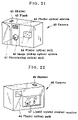
- FIG. 21 is a front perspective schematic illustrative of the outside shape of a digital camera in which the optical path-bending zoom optical system of the invention is built.
- FIG. 22 is a rear perspective schematic of the digital camera of FIG. 21 .
- FIG. 23 is a sectional schematic of the digital camera of FIG. 21 .
- FIG. 24 is a front perspective view of a personal computer in use, in which the optical path-bending zoom optical system of the invention is built as an objective optical system.
- FIG. 25 is a sectional view of a phototaking optical system in the personal computer.
- FIG. 26 is a side view of the state of FIG. 25 .
- FIGS. 27( a ) and 27 ( b ) are a front and a side view of a cellular phone in which the optical path-bending zoom optical system of the 7 invention is built as an objective optical system
- FIG. 20( c ) is a sectional view of a phototaking optical system in the same.
- Example 1 of the zoom lens according to the invention is now explained. Sectional lens configurations of Example 1 at the wide-angle end (a), in the intermediate state (b) and at the telephoto end (c) upon focused on an object point at infinity are shown in FIGS. 1( a ), 1 ( b ) and 1 ( c ).
- the first lens group is indicated by G 1
- the second lens group by G 2
- a stop by S the third lens group by G 3
- the fourth lens group by G 4 a cover glass for an electronic image pickup device CCD by CG
- the image plane of CCD by I the image plane of CCD by I.
- a plane-parallel plate or the taken-apart optical path-bending prism in the first lens group G 1 is indicated by P. It is noted that in addition to the near-infrared sharp cut coat, it is acceptable to use an infrared cut absorption filter or a transparent plane plate with a near-infrared sharp cut coat applied on its entrance surface. As shown typically in FIG. 2 that is an optical path diagram for Example 1 of the zoom lens upon focused on an infinite object point at the wide-angle end, the optical path-bending prism P is configured as a reflecting prism for bending the optical path through 90°.
- Example 1 is directed to a zoom lens made up of a first lens group G 1 composed of a negative meniscus lens element convex on its object side, an optical path-bending prism P, a double-concave negative lens and a positive meniscus lens convex on its object side, an aperture stop S, a second lens group G 2 composed of a doublet consisting of a positive meniscus lens convex on its object side and a negative meniscus lens convex on its object side and a double-convex positive lens, a third lens group G 3 composed of one positive meniscus lens convex on its object side and a fourth lens group G 4 composed of one positive meniscus lens convex on its object side.
- a zoom lens made up of a first lens group G 1 composed of a negative meniscus lens element convex on its object side, an optical path-bending prism P, a double-concave negative lens and a positive meniscus lens convex on its object side, an aperture stop S, a second lens group G 2 composed of a
- the first lens group G 1 and the fourth lens group G 4 remain fixed, and the aperture stop S, the second lens group G 2 and the third lens group G 3 move toward the object side.
- the third lens group G 3 moves toward the object side.
- Five aspheric surfaces are used; one at the image side-surface of the negative meniscus lens convex on its object side in the first lens group G 1 , two at both the surfaces of the double-concave lens in the first lens group G 1 , one at the surface located nearest to the object side in the second lens group G 2 , and one at the surface facing the object side in the fourth lens group G 4 .
- x be an optical axis on condition that the direction of propagation of light is positive and y be a direction orthogonal to the optical axis.
- r is a paraxial radius of curvature
- K is a conical coefficient
- a 4 , A 6 , A 8 and A 10 are the fourth, sixth, eighth and tenth aspheric coefficients, respectively.
- FIGS. 3( a ), 3 ( b ) and 3 ( c ) are aberration diagrams for Example 1 upon focused on an infinite object point, wherein (a), (b) and (c) represent spherical aberrations SA, astigmatism AS, distortion DT and chromatic aberration of magnification CC at the wide-angle end, in the intermediate state and at the telephoto end, respectively.
- FIGS. 4-10 are illustrative of the horizontal wave optics MTF (modulation transfer function) characteristics of the central areas of the respective screens.
- the F-number at the wide-angle end is 2.80
- the horizontal pixel pitch of the image pickup device used is 2.5 ⁇ m (Nyquist frequency 200 cycles/mm).
- FIG. 4 is indicative of MTF at full aperture at the wide-angle end (F/2.80).
- FIG. 5 is illustrative of MTF at full aperture at an intermediate distance (F/3.56).
- FIG. 6 is illustrative of MTF at full aperture at the telephoto end (F/4.55).
- FIG. 7 is illustrative of MTF at a two-stop aperture at the wide-angle end (F/5.60).
- FIG. 8 is illustrative of MTF at a two-stop aperture at an intermediate distance (F/7.12).
- FIG. 9 is illustrative of MTF at a two-stop aperture at the telephoto end (F/9.10).
- FIG. 10 is illustrative of the case where the horizontal wave optics MTF is high.
- the solid line (a) indicates horizontal MTF for the zoom lens system itself.
- the one-dotted line (b) indicates horizontal MTF when the zoom lens system is provided with the optical LPF.
- the dotted line (c) indicates horizontal alias components upon removal of the optical LPF.
- a white weight as mentioned below was used at the respective wavelengths in nm.
- the solid line and the one-dotted line show much the same tendency, as shown in FIGS. 4-10 .
- the optical low-pass filter is generally inserted between an image-formation lens system and an image pickup device to remove low-frequency components from the alias components.
- FIG. 11 is illustrative of the shape of the stop at full aperture
- FIG. 12 is illustrative of the shape of the stop at a two-stop aperture.
- OP stands for an optical axis
- Da six stop plates and Xa and Xb apertures.
- the stop has only two aperture shapes, i.e., those defined by a full-aperture state ( FIG. 11 ) and an f-stop number that is the F-number that satisfies a given condition (two-stop; FIG. 12 ).
- the aperture shape of the stop that determines the F-number can remain constantly fixed. With such an arrangement using the stop of fixed shape, the thickness of the stop mechanism can be reduced. It is thus possible to make the lens-to-lens spacing with the stop interposed therein shorter than ever before and, hence, cut down the length of the zoom lens system.
- a detachable ND filter may be interposed between other lens groups.
- FIG. 13 is illustrative of one exemplary pixel array for the electronic image pickup device, wherein R (red), G (green) and B (blue) pixels or four pixels, i.e., cyan, magenta, yellow and green (G) pixels (see FIG. 15 ) are mosaically arranged at the pixel spacing a.
- the “effective image pickup plane” used herein is understood to mean a certain area in the photoelectric conversion surface on an image pickup device used for the reproduction of a phototaken image (on a personal computer or by a printer).
- the diagonal length L of an effective image pickup plane is thus defined by that of the effective image pickup plane.
- the image pickup range used for image reproduction may be variable, it is noted that when the zoom lens of the present invention is used on an image pickup apparatus having such functions, the diagonal length L of its effective image pickup plane varies. In that case, the diagonal length L of the effective image pickup plane according to the present invention is defined by the maximum value in the widest possible range for L.
- a near-infrared cut filter or a near-infrared cut coat surface on the image side of the final lens group there is provided a near-infrared cut filter or a near-infrared cut coat surface.
- This near-infrared cut filter or near-infrared cut coat surface is designed to have a transmittance of at least 80% at 600 nm wavelength and a transmittance of up to 10% at 700 nm wavelength. More specifically, the near-infrared cut filter or the near-infrared sharp cut coat has a multilayer structure made up of such 27 layers as mentioned below; however, the design wavelength is 780 nm.
- Substrate Material Physical Thickness (nm) ⁇ /4 1st layer Al 2 O 3 58.96 0.50 2nd layer TiO 2 84.19 1.00 3rd layer SiO 2 134.14 1.00 4th layer TiO 2 84.19 1.00 5th layer SiO 2 134.14 1.00 6th layer TiO 2 84.19 1.00 7th layer SiO 2 134.14 1.00 8th layer TiO 2 84.19 1.00 9th layer SiO 2 134.14 1.00 10th layer TiO 2 84.19 1.00 11th layer SiO 2 134.14 1.00 12th layer TiO 2 84.19 1.00 13th layer SiO 2 134.14 1.00 14th layer TiO 2 84.19 1.00 15th layer SiO 2 178.41 1.33 16th layer TiO 2 101.03 1.21 17th layer SiO 2 167.67 1.25 18th layer TiO 2 96.82 1.15 19th layer SiO 2 147.55 1.05 20th layer TiO 2 84
- the aforesaid near-infrared sharp cut coat has such transmittance characteristics as shown in FIG. 14 .
- that filter or coat should preferably be designed such that the ratio of the transmittance of 420 nm wavelength with respect to the transmittance of a wavelength in the range of 400 nm to 700 nm at which the highest transmittance is found is at least 15% and that the ratio of 400 nm wavelength with respect to the highest wavelength transmittance is up to 6%. It is thus possible to reduce a discernible difference between the colors perceived by the human eyes and the colors of the image to be picked up and reproduced. In other words, it is possible to prevent image degradation due to the fact that a color of short wavelength less likely to be perceived through the human sense of sight can be readily seen by the human eyes.
- the image pickup plane I of a CCD is provided thereon with a complementary colors mosaic filter wherein, as shown in FIG. 15 , color filter elements of four colors, cyan, magenta, yellow and green are arranged in a mosaic fashion corresponding to image pickup pixels. More specifically, these four different color filter elements, used in almost equal numbers, are arranged in such a mosaic fashion that neighboring pixels do not correspond to the same type of color filter elements, thereby ensuring more faithful color reproduction.
- the complementary colors mosaic filter is composed of at least four different color filter elements as shown in FIG. 15 , which should preferably have such characteristics as given below.
- the green, yellow and cyan filter elements have a strength of at least 80% at 530 nm wavelength with respect to their respective spectral strength peaks, and the magenta filter elements have a strength of 10% to 50% at 530 nm wavelength with their spectral strength peak.
- the green filter element G has a spectral strength peak at 525 nm.
- the yellow filter element Y e has a spectral strength peak at 555 nm.
- the cyan filter element C has a spectral strength peak at 510 nm.
- the magenta filter element M has peaks at 445 nm and 620 nm.
- the respective color filter elements have, with respect to their respective spectral strength peaks, strengths of 99% for G, 95% for Y e , 97% for C and 38% for M.
- Such signal processing as mentioned below is electrically carried out by means of a controller (not shown) (or a controller used with digital cameras).
- FIG. 17 Details of the aperture stop portion in each example are shown in perspective in FIG. 17 in conjunction with a four-group arrangement, wherein the first lens group G 1 excepting the optical path-bending prism P is shown.
- a turret 10 capable of brightness control at 0 stage, ⁇ 1 stage, ⁇ 2 stage, ⁇ 3 stage and ⁇ 4 stage.
- the turret 10 is composed of an aperture 1 A for 0 stage control, which is defined by a circular fixed space of about 4 mm in diameter (with a transmittance of 100% with respect to 550 nm wavelength), an aperture 1 B for ⁇ 1 stage correction, which is defined by a transparent plane-parallel plate having a fixed aperture shape with an aperture area nearly half that of the aperture 1 A (with a transmittance of 99% with respect to 550 nm wavelength), and circular apertures 1 C, 1 D and 1 E for ⁇ 2, ⁇ 3 and ⁇ 4 stage corrections, which have the same aperture area as that of the aperture 1 B and are provided with ND filters having the respective transmittances of 50%, 25% and 13% with respect to 550 nm wavelength.
- turret 10 ′ shown in the front view of FIG. 18 .
- This turret 10 ′ capable of brightness control at 0 stage, ⁇ 1 stage, ⁇ 2 stage, ⁇ 3 stage and ⁇ 4 stage is located at the aperture stop position on the optical axis between the first lens group G 1 and the second lens group G 2 in the image pickup optical system.
- the turret 10 ′ is composed of an aperture 1 A′ for 0 stage control, which is defined by a circular fixed space of about 4 mm in diameter, an aperture 1 B′ for ⁇ 1 stage correction, which is of a fixed aperture shape with an aperture area nearly half that of the aperture 1 A′, and apertures 1 C′, 1 D′ and 1 E′ for ⁇ 2, ⁇ 3 and ⁇ 4 stage corrections, which are of fixed shape with decreasing areas in this order.
- FIG. 19 is illustrative of CCD image pickup operation wherein signals are sequentially read in the interlaced scanning mode.
- Pa, Pb and Pc are photosensitive blocks using photodiodes
- Va, Vb and Vc are CCD vertical transfer blocks
- Ha is a CCD horizontal transfer block.
- the A field is an odd-number field and the B field is an even-number field.
- the basic operation takes place in the following order: (1) accumulation of signal charges by light at the photosensitive block (photoelectric conversion), (2) shift of signal charges from the photosensitive block to the vertical transfer block (field shift), (3) transfer of signal charges at the vertical transfer block (vertical transfer), (4) transfer of signal charges from the vertical transfer block to the horizontal transfer block (line shift), (5) transfer of signal charges at the horizontal transfer block (horizontal transfer), and (6) detection of signal charges at the output end of the horizontal transfer block (detection).
- Such sequential reading may be carried out using either one of the A field (odd-number field) and the B field (even-number field).
- the timing of accumulation at the A field and the B field lags by 1/60.
- a frame image is constructed as a DSC (digital spectrum compatible) image, there is blurring such as a double image in the case of a subject in motion.
- the A field and B field are simultaneously exposed to light to mix signals at adjacent fields. After processed by a mechanical shutter upon the completion of exposure, signals are independently read from the A field and the B field for signal synthesis.
- FIG. 20 is illustrative of CCD image pickup operation wherein the sequential reading of signals is performed in the progressive mode.
- Vd, Ve and Vf are CCD vertical transfer blocks and Hb is a CCD horizontal transfer block.
- signals are read in order of the arranged pixels, so that charge accumulation reading operation can be all electronically controlled. Accordingly, exposure time can be cut down to about ( 1/10,000 second).
- the arrangement of FIG. 20 has the demerit of making it more difficult to achieve size reductions because of an increased number of vertical CCDs as compared with the arrangement of FIG. 19 .
- the invention is applicable to the mode of FIG. 19 as well as to the mode of FIG. 20 because of such merits as mentioned above.
- the present electronic imaging system constructed as described above may be applied to phototaking systems where object images formed through zoom lenses are received at image pickup devices such as CCDs or silver-halide films, inter alia, digital cameras or video cameras as well as PCs and telephone sets which are typical information processors, in particular, easy-to-carry cellular phones. Given below are some such embodiments.
- image pickup devices such as CCDs or silver-halide films, inter alia, digital cameras or video cameras as well as PCs and telephone sets which are typical information processors, in particular, easy-to-carry cellular phones. Given below are some such embodiments.
- FIGS. 21 , 22 and 23 are conceptual illustrations of a phototaking optical system 41 for digital cameras, in which the image-formation optical system of the invention is built.
- FIG. 21 is a front perspective view of the outside shape of a digital camera 40
- FIG. 22 is a rear perspective view of the same.
- FIG. 23 is a horizontally sectional view of the construction of the digital camera 40 .
- the digital camera 40 comprises a phototaking optical system 41 including a phototaking optical path 42 , a finder optical system 43 including a finder optical path 44 , a shutter 45 , a flash 46 , a liquid crystal monitor 47 and so on.
- a phototaking optical system 41 including a phototaking optical path 42
- a finder optical system 43 including a finder optical path 44
- a shutter 45 a flash 46
- a liquid crystal monitor 47 and so on.
- the optical path-bending zoom lens according to Example 1 the optical path is bent by an optical path-bending prism P in the longitudinal direction of the digital camera 40 , i.e., in the lateral direction so that the camera can be slimmed down.
- An object image formed by the phototaking optical system 41 is formed on the image pickup plane of a CCD 49 via a near-infrared cut filter.
- the object image received at CCD 49 is shown as an electronic image on the liquid crystal monitor 47 via processing means 51 , which monitor is mounted on the back of the camera.
- This processing means 51 is connected with recording means 52 in which the phototaken electronic image may be recorded.
- the recording means 52 may be provided separately from the processing means 51 or, alternatively, it may be constructed in such a way that images are electronically recorded and written therein by means of floppy discs, memory cards, MOs or the like.
- This camera may also be constructed in the form of a silver halide camera using a silver halide film in place of CCD 49 .
- a finder objective optical system 53 is located on the finder optical path 44 .
- An object image formed by the finder objective optical system 53 is in turn formed on the field frame 57 of a Porro prism 55 that is an image-erecting member.
- an eyepiece optical system 59 for guiding an erected image into the eyeball E of an observer. It is here noted that cover members 50 are provided on the entrance sides of the phototaking optical system 41 and finder objective optical system 53 as well as on the exit side of the eyepiece optical system 59 .
- the phototaking optical system 41 is constructed of a fast zoom lens having a high zoom ratio at the wide-angle end with satisfactory aberrations and a back focus large enough to receive a filter, etc. therein.
- the camera can be slimmed down because, as described above, the optical path of the zoom lens is selectively bent in the longitudinal direction of the digital camera 40 . With the optical path bent in the thus selected direction, the flash 46 is positioned above the entrance surface of the phototaking optical system 42 , so that the influences of shadows on strobe shots of figures can be slackened.
- plane-parallel plates are used as the cover members 50 ; however, it is acceptable to use powered lenses. It is understood that depending on ease of camera's layout, the optical path can be bent in either one of the longitudinal and lateral directions.
- FIGS. 24 , 25 and 26 are illustrative of a personal computer that is one example of the information processor in which the image-formation optical system of the invention is built as an objective optical system.
- FIG. 24 is a front perspective view of a personal computer 300 in use
- FIG. 25 is a sectional view of a phototaking optical system 303 in the personal computer 300
- FIG. 26 is a side view of the state of FIG. 24 .
- the personal computer 300 comprises a keyboard 301 via which an operator enters information therein from outside, information processing or recording means (not shown), a monitor 302 on which the information is shown for the operator, and a phototaking optical system 303 for taking an image of the operator and surrounding images.
- the monitor 302 use may be made of a transmission type liquid crystal display device illuminated by backlight (not shown) from the back surface, a reflection type liquid crystal display device in which light from the front is reflected to show images, or a CRT display device.
- the phototaking optical system 303 is shown as being built in the right upper portion of the monitor 302 , it may be located somewhere around the monitor 302 or keyboard 301 .
- This phototaking optical system 303 comprises on a phototaking optical path 304 an objective lens 112 such as one represented by Example 1 of the optical path-bending zoom lens according to the invention and an image pickup device chip 162 for receiving an image. These are built in the personal computer 300 .
- an imaging unit 162 is provided with an image pickup device chip 160 , which can be fitted into the rear end of a lens barrel 113 of the objective lens 112 in one-touch operation.
- the lens barrel 113 is provided at its end (not shown) with a cover glass 114 for protection of the objective lens 112 . It is here noted that driving mechanisms for the zoom lens, etc. contained in the lens barrel 113 are not shown.
- An object image received at the image pickup device chip 162 is entered via a terminal 166 in the processing means of the personal computer 300, and displayed as an electronic image on the monitor 302 .
- an image 305 taken of the operator is shown in FIG. 21 . This image 305 may be displayed on a personal computer on the other end via suitable processing means and the Internet or telephone line.
- FIGS. 27( a ), 27 ( b ) and 27 ( c ) are illustrative of a telephone set that is one example of the information processor in which the image-formation optical system of the invention is built in the form of a phototaking optical system, especially a convenient-to-carry cellular phone.
- FIG. 27( a ) and FIG. 27( b ) are a front and a side view of a cellular phone 400 , respectively
- FIG. 20( c ) is a sectional view of a phototaking optical system 405 .
- the cellular phone 400 comprises a microphone 401 for entering the voice of an operator therein as information, a speaker 402 for producing the voice of the person on the other end, an input dial 403 via which the operator enters information therein, a monitor 404 for displaying an image taken of the operator or the person on the other end and indicating information such as telephone numbers, a phototaking optical system 405 , an antenna 406 for transmitting and receiving communication waves, and processing means (not shown) for processing image information, communication information, input signals, etc.
- the monitor 404 is a liquid crystal display device. It is noted that the components are not necessarily arranged as shown.
- the phototaking optical system 405 comprises on a phototaking optical path 407 an objective lens 112 such as one represented by Example 1 of the optical path-bending zoom lens according to the invention and an image pickup device chip 162 for receiving an object image. These are built in the cellular phone 400 .
- an imaging unit 160 is provided with the image pickup device chip 162 , which can be fitted into the rear end of a lens barrel 113 of the objective lens 112 in one-touch operation.
- the lens barrel 113 is provided at its end (not shown) with a cover glass 114 for protection of the objective lens 112 . It is here noted that driving mechanisms for the zoom lens, etc. contained in the lens barrel 113 are not shown.
- An object image received at the image pickup device chip 162 is entered via a terminal 166 in processing means (not shown), so that the object image can be displayed as an electronic image on the monitor 404 and/or a monitor at the other end.
- the processing means also include a signal processing function for converting information about the object image received at the image pickup device chip 162 into transmittable signals, thereby sending the image to the person at the other end.
Abstract
a≦4 μm (1)
F>a (2)
Here a is the horizontal pixel pitch in μm of the electronic image pickup device and F is the F-number of the zoom lens system at its wide-angle end.
Description
-
- a stop has a constantly fixed aperture shape, and the following conditions (1) and (2) are satisfied:
a≦4 μm (1)
F>a (2) - where a is the horizontal pixel pitch in μm of the electronic image pickup device and F is the F-number of the zoom lens system at its wide-angle end.
- a stop has a constantly fixed aperture shape, and the following conditions (1) and (2) are satisfied:
-
- the following conditions (1) and (2) are satisfied:
a≦4 μm (1)
F>a (2) - where a is the horizontal pixel pitch in μm of the electronic image pickup device and F is the F-number of the zoom lens system at its wide-angle end, and
- the mode of reading signals from the electronic image pickup device has a sequential reading function.
- the following conditions (1) and (2) are satisfied:
1/1.22Fλ
1.22Fλ<2a (a),
i.e., F<1.64a/λ (b)
F<3.0×10³×a/1 mm (c)
3.0×10³×a/1 mm (d)
it is possible to reduce the influence of diffraction and make the range of light quantity control wide. Here, the maximum F-number upon stopping-down is defined by
(maximum F-number at the wide-angle end+maximum F-number at the telephoto end)/2
This value is hereinafter called F′. It is then preferable to satisfy
2.0×10³ ×a/1 mm<F′<4.5×10³ ×a/1 mm (3)
F′=(5.60+9.10)/2=7.35 (4)
F′/(a/1 mm)=[7.35/(2.5 μm/1 mm)]=2.94×10³ (5)
The ratio between the maximum F-number at the wide-angle end (maximum F-number) and the minimum F-number at the telephoto end is set at
Max. F w/Min. F w=5.60/2.80=2.00 (6)
τ600/τ550≧0.8 (7)
τ700/τ550≦0.08 (8)
where τ550 is the transmittance at 550 nm wavelength.
τ600/τ550≧0.85 (7)′
τ700/τ550≦0.05 (8)′
τ600/τ550≧0.9 (7)″
τ700/τ550≦0.03 (8)″
τ400/τ550≦0.08 (9)
τ440/τ550≧0.4 (10)
τ400/τ550≦0.06 (9)′
τ440/τ550≧0.5 (10)′
τ400/τ550≦0.04 (9)″
τ440/τ550≧0.6 (10)″
- f: focal length of the zoom lens system
- FNO: F-number
- ω: half angle of view
- WE: wide-angle end
- ST: intermediate state
- TE: telephoto end
- r1, r2, . . . : radius of curvature of each lens surface
- d1, d2, . . . : spacing between the adjacent lens surfaces
- nd1, nd2, . . . : d-line refractive index of each lens
- νd1, νd2, . . . : Abbe number of each lens
x=(y 2 /r)/[1+{1−(K+1)(y/r)2}1/2 ]+A 4 y 4 +A 6 y 6 +A 8 y 8 +A 10 y 10
where r is a paraxial radius of curvature, K is a conical coefficient, and A4, A6, A8 and A10 are the fourth, sixth, eighth and tenth aspheric coefficients, respectively.
| r1 = | 20.9756 | d1 = | 1.1000 | nd = | 1.69350 | νd1 = | 53.21 |
| r2 = | 9.4120 | d2 = | 3.0000 | ||||
| (Aspheric) | |||||||
| r3 = | ∞ | d3 = | 12.5000 | nd = | 1.80610 | νd1 = | 40.92 |
| r4 = | ∞ | d4 = | 0.4000 | ||||
| r5 = | −24.1584 | d5 = | 0.9000 | nd = | 1.69350 | νd1 = | 53.21 |
| (Aspheric) | |||||||
| r6 = | 19.1724 | d6 = | 0.4000 | ||||
| (Aspheric) | |||||||
| r7 = | 7.6644 | d7 = | 1.9000 | nd = | 1.84666 | νd1 = | 23.78 |
| r8 = | 10.3296 | d8 = | (Variable) | ||||
| r9 = | ∞ (Stop) | d9 = | 1.0000 | ||||
| r10 = | 7.2754 | d10 = | 3.9827 | nd = | 1.74320 | νd1 = | 49.34 |
| (Aspheric) | |||||||
| r11 = | 21.4424 | d11 = | 0.7000 | nd = | 1.84666 | νd1 = | 23.78 |
| r12 = | 6.8156 | d12 = | 0.8000 | ||||
| r13 = | 20.8730 | d13 = | 1.5000 | nd = | 1.72916 | νd1 = | 54.68 |
| r14 = | −30.7312 | d14 = | (Variable) | ||||
| r15 = | 14.1761 | d15 = | 1.4000 | nd = | 1.48749 | νd1 = | 70.23 |
| r16 = | 206.1638 | d16 = | (Variable) | ||||
| r17 = | 17.4404 | d17 = | 1.2000 | nd = | 1.49236 | νd1 = | 57.86 |
| (Aspheric) | |||||||
| r18 = | 37.3185 | d18 = | 2.3900 | ||||
| r19 = | ∞ | d19 = | 0.6000 | nd = | 1.51633 | νd1 = | 64.14 |
| r20 = | ∞ | d20 = | 1.3596 | ||||
| r21 = | ∞ | ||||||
| (Image Plane) | |||||||
| Aspherical Coefficients |
| Second surface | |||
| K = | 0 | ||
| A4 = | −7.0154 × 10⁻⁵ | ||
| A6 = | −7.0164 × 10⁻⁷ | ||
| A8 = | −1.4330 × 10⁻⁸ | ||
| A10 = | 0.0000 | ||
| 5th surface | |||
| K = | 0 | ||
| A4 = | −1.2550 × 10⁻³ | ||
| A6 = | −1.8493 × 10⁻⁵ | ||
| A8 = | 1.8668 × 10⁻⁷ | ||
| A10 = | 0.0000 | ||
| 6th surface | |||
| K = | 0 | ||
| A4 = | 1.4852 × 10⁻³ | ||
| A6 = | −1.1617 × 10⁻⁵ | ||
| A8 = | 2.8181 × 10⁻⁷ | ||
| A10 = | 0.0000 | ||
| 10th surface | |||
| K = | 0 | ||
| A4 = | −1.6552 × 10⁻⁴ | ||
| A6 = | 2.4503 × 10⁻⁶ | ||
| A8 = | −2.3665 × 10⁻⁷ | ||
| A10 = | 0.0000 | ||
| 17th surface | |||
| K = | 0 | ||
| A4 = | −2.6614 × 10⁻⁴ | ||
| A6 = | 7.0171 × 10⁻⁶ | ||
| A8 = | −3.8288 × 10⁻⁷ | ||
| A10 = | 0.0000 | ||
| Zooming Data (∞) |
| WE | ST | TE | |||
| f (mm) | 6.00332 | 10.39732 | 17.99812 | ||
| FNO | 2.8012 | 3.5601 | 4.5471 | ||
| 2ω (°) | 32.6 | 19.4 | 11.3 | ||
| d8 | 17.12225 | 8.06116 | 1.49972 | ||
| d14 | 1.39980 | 6.51338 | 2.30699 | ||
| d16 | 8.84122 | 12.79373 | 23.55661 | ||
| Wavelength | 656.28 | 587.56 | 546.07 | 486.13 | 435.84 | 404.66 |
| (nm) | ||||||
| White Weight | 0.3 | 0.6 | 1.0 | 0.6 | 0.3 | 0.02 |
| Substrate | Material | Physical Thickness (nm) | λ/4 | ||
| 1st layer | Al2O3 | 58.96 | 0.50 | ||
| 2nd layer | TiO2 | 84.19 | 1.00 | ||
| 3rd layer | SiO2 | 134.14 | 1.00 | ||
| 4th layer | TiO2 | 84.19 | 1.00 | ||
| 5th layer | SiO2 | 134.14 | 1.00 | ||
| 6th layer | TiO2 | 84.19 | 1.00 | ||
| 7th layer | SiO2 | 134.14 | 1.00 | ||
| 8th layer | TiO2 | 84.19 | 1.00 | ||
| 9th layer | SiO2 | 134.14 | 1.00 | ||
| 10th layer | TiO2 | 84.19 | 1.00 | ||
| 11th layer | SiO2 | 134.14 | 1.00 | ||
| 12th layer | TiO2 | 84.19 | 1.00 | ||
| 13th layer | SiO2 | 134.14 | 1.00 | ||
| 14th layer | TiO2 | 84.19 | 1.00 | ||
| 15th layer | SiO2 | 178.41 | 1.33 | ||
| 16th layer | TiO2 | 101.03 | 1.21 | ||
| 17th layer | SiO2 | 167.67 | 1.25 | ||
| 18th layer | TiO2 | 96.82 | 1.15 | ||
| 19th layer | SiO2 | 147.55 | 1.05 | ||
| 20th layer | TiO2 | 84.19 | 1.00 | ||
| 21st layer | SiO2 | 160.97 | 1.20 | ||
| 22nd layer | TiO2 | 84.19 | 1.00 | ||
| 23rd layer | SiO2 | 154.26 | 1.15 | ||
| 24th layer | TiO2 | 95.13 | 1.13 | ||
| 25th layer | SiO2 | 160.97 | 1.20 | ||
| 26th layer | TiO2 | 99.34 | 1.18 | ||
| 27th layer | SiO2 | 87.19 | 0.65 | ||
| Air | |||||
-
- Each green color filter element G has a spectral strength peak at a wavelength Gp,
- each yellow filter element Ye has a spectral strength peak at a wavelength Yp,
- each cyan filter element C has a spectral strength peak at a wavelength Cp, and
- each magenta filter element M has spectral strength peaks at wavelengths MP1 and MP2, and these wavelengths satisfy the following conditions.
510 nm<GP<540 nm
5 nm<Y P −G P<35 nm
−100 nm<C P −G P<−5 nm
430 nm<M P1<480 nm
580 nm<MP2<640 nm
Y=|G+M+Y e +C|×¼
For chromatic signals,
R−Y=|(M+Y e)−(G+C)|
B−Y=|(M+C)−(G+Y e)|
Through this signal processing, the signals from the complementary colors filter are converted into R (red), G (green) and B (blue) signals. In this regard, it is noted that the aforesaid near-infrared sharp cut coat may be located anywhere on the optical path
Claims (10)
a≦4 μm (1)
F>a (2)
a≦2.5 μm (1′)
F>a (2)
a≦4 μm (1)
F>a (2)
τ600/τ550≧0.8 (7)
τ700/τ550≦0.08 (8)
a≦4 μm (1)
F>a (2)
τ600/τ550≧0.8 (7)
τ700/τ550≦0.08 (8)
a≦2.5 μm (1′)
F>a (2)
Applications Claiming Priority (2)
| Application Number | Priority Date | Filing Date | Title |
|---|---|---|---|
| JP2002209560A JP4290935B2 (en) | 2002-07-18 | 2002-07-18 | Electronic imaging device |
| JP2002-209560 | 2002-07-18 |
Publications (2)
| Publication Number | Publication Date |
|---|---|
| US20040021783A1 US20040021783A1 (en) | 2004-02-05 |
| US7436449B2 true US7436449B2 (en) | 2008-10-14 |
Family
ID=31184348
Family Applications (1)
| Application Number | Title | Priority Date | Filing Date |
|---|---|---|---|
| US10/618,675 Expired - Fee Related US7436449B2 (en) | 2002-07-18 | 2003-07-15 | Electronic imaging system |
Country Status (2)
| Country | Link |
|---|---|
| US (1) | US7436449B2 (en) |
| JP (1) | JP4290935B2 (en) |
Cited By (8)
| Publication number | Priority date | Publication date | Assignee | Title |
|---|---|---|---|---|
| US20070052834A1 (en) * | 2005-09-02 | 2007-03-08 | Konica Minolta Photo Imaging, Inc. | Image-taking apparatus, magnification variation control method, and lens unit |
| US20090195646A1 (en) * | 2006-05-11 | 2009-08-06 | Michael Ganser | Microscope comprising a camera connection and a camera adapter |
| US20090322928A1 (en) * | 2008-06-27 | 2009-12-31 | Robinson M Dirk | Electro-optic imaging system with aberrated triplet lens compensated by digital image processing |
| US20100128360A1 (en) * | 2008-11-27 | 2010-05-27 | Canon Kabushiki Kaisha | Zoom lens and image pickup apparatus having the same |
| US20100259667A1 (en) * | 2009-04-08 | 2010-10-14 | Hon Hai Precision Industry Co., Ltd. | Camera module for taking wide angle images and portable electronic device having same |
| US20110164298A1 (en) * | 2008-10-14 | 2011-07-07 | Seiko Precision Inc. | Blade drive device and optical device |
| US8331048B1 (en) * | 2009-12-18 | 2012-12-11 | Bausch & Lomb Incorporated | Methods of designing lenses having selected depths of field |
| US20130250160A1 (en) * | 2012-03-25 | 2013-09-26 | Iain A. Neil | Zoom lens with forward-located aperture stop |
Families Citing this family (24)
| Publication number | Priority date | Publication date | Assignee | Title |
|---|---|---|---|---|
| US7490774B2 (en) * | 2003-11-13 | 2009-02-17 | Metrologic Instruments, Inc. | Hand-supportable imaging based bar code symbol reader employing automatic light exposure measurement and illumination control subsystem integrated therein |
| US7128266B2 (en) * | 2003-11-13 | 2006-10-31 | Metrologic Instruments. Inc. | Hand-supportable digital imaging-based bar code symbol reader supporting narrow-area and wide-area modes of illumination and image capture |
| US7594609B2 (en) * | 2003-11-13 | 2009-09-29 | Metrologic Instruments, Inc. | Automatic digital video image capture and processing system supporting image-processing based code symbol reading during a pass-through mode of system operation at a retail point of sale (POS) station |
| TWI268397B (en) * | 2002-08-23 | 2006-12-11 | Pentax Corp | Digital camera |
| JP3896988B2 (en) * | 2003-05-12 | 2007-03-22 | コニカミノルタフォトイメージング株式会社 | Imaging lens device |
| US7841533B2 (en) | 2003-11-13 | 2010-11-30 | Metrologic Instruments, Inc. | Method of capturing and processing digital images of an object within the field of view (FOV) of a hand-supportable digitial image capture and processing system |
| JP4806943B2 (en) * | 2005-03-11 | 2011-11-02 | 株式会社ニコン | Zoom lens |
| JP4670300B2 (en) * | 2004-09-30 | 2011-04-13 | 株式会社ニコン | Zoom lens |
| US7568628B2 (en) | 2005-03-11 | 2009-08-04 | Hand Held Products, Inc. | Bar code reading device with global electronic shutter control |
| JP2006267391A (en) * | 2005-03-23 | 2006-10-05 | Mitsubishi Electric Corp | Imaging apparatus |
| JP2006293200A (en) * | 2005-04-14 | 2006-10-26 | Nikon Corp | Lens barrel of camera |
| JP4844012B2 (en) * | 2005-05-26 | 2011-12-21 | コニカミノルタオプト株式会社 | Variable magnification optical system and imaging apparatus |
| US7770799B2 (en) | 2005-06-03 | 2010-08-10 | Hand Held Products, Inc. | Optical reader having reduced specular reflection read failures |
| JP4951915B2 (en) * | 2005-09-28 | 2012-06-13 | 株式会社ニコン | Zoom lens |
| JP4823666B2 (en) | 2005-12-05 | 2011-11-24 | Hoya株式会社 | Zoom lens system |
| JP2007193194A (en) * | 2006-01-20 | 2007-08-02 | Canon Inc | Imaging apparatus |
| US7626768B2 (en) | 2006-02-13 | 2009-12-01 | Casio Computer Co., Ltd. | Zoom lens and camera with zoom lens |
| US7453651B2 (en) | 2006-02-28 | 2008-11-18 | Casio Computer Co., Ltd. | Zoom lens and camera with zoom lens |
| JP5282314B2 (en) * | 2010-05-19 | 2013-09-04 | コニカミノルタ株式会社 | Zoom lens and imaging device |
| JP5240323B2 (en) * | 2010-09-30 | 2013-07-17 | 株式会社ニコン | Interchangeable lens and camera body |
| CN102445818B (en) * | 2010-09-30 | 2016-09-14 | 株式会社尼康 | Change camera lens and camera body |
| US9030597B2 (en) | 2010-09-30 | 2015-05-12 | Nikon Corporation | Interchangeable lens and camera body |
| EP3370410B1 (en) * | 2015-10-26 | 2020-11-25 | Kyocera Corporation | Imaging device |
| CN107230232B (en) * | 2017-04-27 | 2020-06-30 | 东南大学 | F number matching method of focusing light field camera |
Citations (27)
| Publication number | Priority date | Publication date | Assignee | Title |
|---|---|---|---|---|
| US3971065A (en) * | 1975-03-05 | 1976-07-20 | Eastman Kodak Company | Color imaging array |
| US4290675A (en) * | 1978-12-04 | 1981-09-22 | Leo Beiser | Anaglyph stereoscopy |
| US4759347A (en) * | 1981-09-12 | 1988-07-26 | Fuji Photo Optical Company, Ltd. | Endoscope apparatus using solid state image pickup device |
| JPS63292106A (en) | 1987-05-26 | 1988-11-29 | Olympus Optical Co Ltd | Variable power lens |
| JPH03139607A (en) | 1989-10-26 | 1991-06-13 | Olympus Optical Co Ltd | Power varying lens |
| JPH03158817A (en) | 1989-11-17 | 1991-07-08 | Olympus Optical Co Ltd | Variable power lens |
| JPH09211287A (en) | 1996-01-31 | 1997-08-15 | Canon Inc | Image pickup device |
| US5668668A (en) | 1995-03-08 | 1997-09-16 | Nikon Corporation | Zoom lens with five lens groups |
| JPH11194274A (en) | 1998-01-05 | 1999-07-21 | Ricoh Co Ltd | Zoom lens |
| JP2000137164A (en) | 1998-10-30 | 2000-05-16 | Nikon Corp | Zoom lens |
| US6088059A (en) * | 1995-12-26 | 2000-07-11 | Olympus Optical Co., Ltd. | Electronic imaging apparatus having image quality-improving means |
| US6088169A (en) | 1998-02-27 | 2000-07-11 | Fuji Photo Optical Co., Ltd. | Wide-angle zoom lens |
| JP2000244799A (en) | 1999-02-22 | 2000-09-08 | Olympus Optical Co Ltd | Image pickup device |
| US6124987A (en) | 1998-06-26 | 2000-09-26 | Fuji Photo Film Co., Ltd. | Zoom Lens |
| JP2000275520A (en) | 1999-03-24 | 2000-10-06 | Minolta Co Ltd | Zoom lens |
| US6178046B1 (en) * | 1999-04-21 | 2001-01-23 | Intel Corporation | Anti-aliasing diffractive aperture and method of using same |
| US6229655B1 (en) | 1998-12-22 | 2001-05-08 | Minolta Co., Ltd. | Zoom lens system |
| US6308011B1 (en) | 1998-03-31 | 2001-10-23 | Canon Kabushiki Kaisha | Zoom lens and photographic apparatus having the same |
| US20020027721A1 (en) * | 2000-07-10 | 2002-03-07 | Shinichi Mihara | Electronic picture taking apparatus having a zoom lens system |
| US6417973B2 (en) * | 2000-05-23 | 2002-07-09 | Olympus Optical Co., Ltd. | Electronic image pickup equipment |
| US6741760B2 (en) * | 1997-03-17 | 2004-05-25 | Minaltacco., Ltd. | Image sensing apparatus which intentionally retains longitudinal chromatic aberration |
| US6905462B1 (en) * | 1999-09-08 | 2005-06-14 | Olympus Corporation | Endoscope image pickup optical system |
| US6992720B2 (en) * | 2000-12-08 | 2006-01-31 | Canon Kabushiki Kaisha | Optical apparatus including image pick-up device and interchangeable lens with controller for controlling change of aperture |
| US7038722B2 (en) * | 2001-03-19 | 2006-05-02 | Canon Kabushiki Kaisha | Optical imaging system for suppressing the generation of red-toned ghosting particularly when there is background light |
| US7098955B2 (en) * | 2000-10-26 | 2006-08-29 | Canon Kabushiki Kaisha | Optical apparatus operable in static and dynamic image taking modes |
| US7136230B2 (en) * | 2001-01-18 | 2006-11-14 | Olympus Corporation | Image pickup system |
| US7151570B2 (en) * | 2000-12-21 | 2006-12-19 | Canon Kabushiki Kaisha | Imaging apparatus with interchangeable lens apparatus, the lens apparatus having a memory for storing optical performance data of the lens apparatus |
-
2002
- 2002-07-18 JP JP2002209560A patent/JP4290935B2/en not_active Expired - Fee Related
-
2003
- 2003-07-15 US US10/618,675 patent/US7436449B2/en not_active Expired - Fee Related
Patent Citations (29)
| Publication number | Priority date | Publication date | Assignee | Title |
|---|---|---|---|---|
| US3971065A (en) * | 1975-03-05 | 1976-07-20 | Eastman Kodak Company | Color imaging array |
| US4290675A (en) * | 1978-12-04 | 1981-09-22 | Leo Beiser | Anaglyph stereoscopy |
| US4759347A (en) * | 1981-09-12 | 1988-07-26 | Fuji Photo Optical Company, Ltd. | Endoscope apparatus using solid state image pickup device |
| JPS63292106A (en) | 1987-05-26 | 1988-11-29 | Olympus Optical Co Ltd | Variable power lens |
| JPH03139607A (en) | 1989-10-26 | 1991-06-13 | Olympus Optical Co Ltd | Power varying lens |
| JPH03158817A (en) | 1989-11-17 | 1991-07-08 | Olympus Optical Co Ltd | Variable power lens |
| US5721642A (en) | 1995-03-08 | 1998-02-24 | Nikon Corporation | Zoom lens |
| US5668668A (en) | 1995-03-08 | 1997-09-16 | Nikon Corporation | Zoom lens with five lens groups |
| US5798871A (en) | 1995-03-08 | 1998-08-25 | Nikon Corporation | Zoom lens |
| US6088059A (en) * | 1995-12-26 | 2000-07-11 | Olympus Optical Co., Ltd. | Electronic imaging apparatus having image quality-improving means |
| JPH09211287A (en) | 1996-01-31 | 1997-08-15 | Canon Inc | Image pickup device |
| US6741760B2 (en) * | 1997-03-17 | 2004-05-25 | Minaltacco., Ltd. | Image sensing apparatus which intentionally retains longitudinal chromatic aberration |
| JPH11194274A (en) | 1998-01-05 | 1999-07-21 | Ricoh Co Ltd | Zoom lens |
| US6088169A (en) | 1998-02-27 | 2000-07-11 | Fuji Photo Optical Co., Ltd. | Wide-angle zoom lens |
| US6308011B1 (en) | 1998-03-31 | 2001-10-23 | Canon Kabushiki Kaisha | Zoom lens and photographic apparatus having the same |
| US6124987A (en) | 1998-06-26 | 2000-09-26 | Fuji Photo Film Co., Ltd. | Zoom Lens |
| JP2000137164A (en) | 1998-10-30 | 2000-05-16 | Nikon Corp | Zoom lens |
| US6229655B1 (en) | 1998-12-22 | 2001-05-08 | Minolta Co., Ltd. | Zoom lens system |
| JP2000244799A (en) | 1999-02-22 | 2000-09-08 | Olympus Optical Co Ltd | Image pickup device |
| JP2000275520A (en) | 1999-03-24 | 2000-10-06 | Minolta Co Ltd | Zoom lens |
| US6178046B1 (en) * | 1999-04-21 | 2001-01-23 | Intel Corporation | Anti-aliasing diffractive aperture and method of using same |
| US6905462B1 (en) * | 1999-09-08 | 2005-06-14 | Olympus Corporation | Endoscope image pickup optical system |
| US6417973B2 (en) * | 2000-05-23 | 2002-07-09 | Olympus Optical Co., Ltd. | Electronic image pickup equipment |
| US20020027721A1 (en) * | 2000-07-10 | 2002-03-07 | Shinichi Mihara | Electronic picture taking apparatus having a zoom lens system |
| US7098955B2 (en) * | 2000-10-26 | 2006-08-29 | Canon Kabushiki Kaisha | Optical apparatus operable in static and dynamic image taking modes |
| US6992720B2 (en) * | 2000-12-08 | 2006-01-31 | Canon Kabushiki Kaisha | Optical apparatus including image pick-up device and interchangeable lens with controller for controlling change of aperture |
| US7151570B2 (en) * | 2000-12-21 | 2006-12-19 | Canon Kabushiki Kaisha | Imaging apparatus with interchangeable lens apparatus, the lens apparatus having a memory for storing optical performance data of the lens apparatus |
| US7136230B2 (en) * | 2001-01-18 | 2006-11-14 | Olympus Corporation | Image pickup system |
| US7038722B2 (en) * | 2001-03-19 | 2006-05-02 | Canon Kabushiki Kaisha | Optical imaging system for suppressing the generation of red-toned ghosting particularly when there is background light |
Cited By (15)
| Publication number | Priority date | Publication date | Assignee | Title |
|---|---|---|---|---|
| US7557852B2 (en) * | 2005-09-02 | 2009-07-07 | Konica Minolta Photo Imaging, Inc. | Image-taking apparatus, magnification variation control method, and lens unit |
| US20070052834A1 (en) * | 2005-09-02 | 2007-03-08 | Konica Minolta Photo Imaging, Inc. | Image-taking apparatus, magnification variation control method, and lens unit |
| US20090195646A1 (en) * | 2006-05-11 | 2009-08-06 | Michael Ganser | Microscope comprising a camera connection and a camera adapter |
| US8643711B2 (en) * | 2006-05-11 | 2014-02-04 | Leica Microsystems Cms Gmbh | Microscope comprising a camera connection and a camera adapter |
| US7948550B2 (en) * | 2008-06-27 | 2011-05-24 | Ricoh Co., Ltd. | Electro-optic imaging system with aberrated triplet lens compensated by digital image processing |
| US20090322928A1 (en) * | 2008-06-27 | 2009-12-31 | Robinson M Dirk | Electro-optic imaging system with aberrated triplet lens compensated by digital image processing |
| US8254008B2 (en) * | 2008-10-14 | 2012-08-28 | Seiko Precision Inc. | Blade drive device and optical device |
| US20110164298A1 (en) * | 2008-10-14 | 2011-07-07 | Seiko Precision Inc. | Blade drive device and optical device |
| US7869135B2 (en) * | 2008-11-27 | 2011-01-11 | Canon Kabushiki Kaisha | Zoom lens and image pickup apparatus having the same |
| US20100128360A1 (en) * | 2008-11-27 | 2010-05-27 | Canon Kabushiki Kaisha | Zoom lens and image pickup apparatus having the same |
| US20100259667A1 (en) * | 2009-04-08 | 2010-10-14 | Hon Hai Precision Industry Co., Ltd. | Camera module for taking wide angle images and portable electronic device having same |
| CN101859021B (en) * | 2009-04-08 | 2013-02-13 | 鸿富锦精密工业(深圳)有限公司 | Optical imaging system |
| US8331048B1 (en) * | 2009-12-18 | 2012-12-11 | Bausch & Lomb Incorporated | Methods of designing lenses having selected depths of field |
| US20130250160A1 (en) * | 2012-03-25 | 2013-09-26 | Iain A. Neil | Zoom lens with forward-located aperture stop |
| US9250422B2 (en) * | 2012-03-25 | 2016-02-02 | Iain A. Neil | Zoom lens with forward-located aperture stop |
Also Published As
| Publication number | Publication date |
|---|---|
| US20040021783A1 (en) | 2004-02-05 |
| JP2004056362A (en) | 2004-02-19 |
| JP4290935B2 (en) | 2009-07-08 |
Similar Documents
| Publication | Publication Date | Title |
|---|---|---|
| US7436449B2 (en) | Electronic imaging system | |
| US10031322B2 (en) | Electronic image pickup system | |
| US6771432B2 (en) | Zoom lens, and electronic imaging system using the same | |
| US7414665B2 (en) | Imaging system | |
| US7420611B2 (en) | Electronic image pickup system | |
| US7046460B2 (en) | Image-formation optical system, and imaging system | |
| US7177094B2 (en) | Zoom lens, and electronic imaging system using the same | |
| US7142371B2 (en) | Zoom lens, and electronic imaging system using the same | |
| US6865026B2 (en) | Zoom lens, and electronic imaging system using the same | |
| US7102830B2 (en) | Electronic imaging system |
Legal Events
| Date | Code | Title | Description |
|---|---|---|---|
| AS | Assignment |
Owner name: OLYMPUS OPTICAL CO., LTD., JAPAN Free format text: ASSIGNMENT OF ASSIGNORS INTEREST;ASSIGNOR:MIHARA, SHINICHI;REEL/FRAME:014299/0141 Effective date: 20030708 |
|
| STCF | Information on status: patent grant |
Free format text: PATENTED CASE |
|
| FEPP | Fee payment procedure |
Free format text: PAYOR NUMBER ASSIGNED (ORIGINAL EVENT CODE: ASPN); ENTITY STATUS OF PATENT OWNER: LARGE ENTITY |
|
| FPAY | Fee payment |
Year of fee payment: 4 |
|
| FPAY | Fee payment |
Year of fee payment: 8 |
|
| AS | Assignment |
Owner name: OLYMPUS CORPORATION, JAPAN Free format text: CHANGE OF ADDRESS;ASSIGNOR:OLYMPUS CORPORATION;REEL/FRAME:039344/0502 Effective date: 20160401 |
|
| FEPP | Fee payment procedure |
Free format text: MAINTENANCE FEE REMINDER MAILED (ORIGINAL EVENT CODE: REM.); ENTITY STATUS OF PATENT OWNER: LARGE ENTITY |
|
| LAPS | Lapse for failure to pay maintenance fees |
Free format text: PATENT EXPIRED FOR FAILURE TO PAY MAINTENANCE FEES (ORIGINAL EVENT CODE: EXP.); ENTITY STATUS OF PATENT OWNER: LARGE ENTITY |
|
| STCH | Information on status: patent discontinuation |
Free format text: PATENT EXPIRED DUE TO NONPAYMENT OF MAINTENANCE FEES UNDER 37 CFR 1.362 |
|
| FP | Lapsed due to failure to pay maintenance fee |
Effective date: 20201014 |