US7326589B2 - Method for producing a TFA image sensor and one such TFA image sensor - Google Patents
Method for producing a TFA image sensor and one such TFA image sensor Download PDFInfo
- Publication number
- US7326589B2 US7326589B2 US11/271,492 US27149205A US7326589B2 US 7326589 B2 US7326589 B2 US 7326589B2 US 27149205 A US27149205 A US 27149205A US 7326589 B2 US7326589 B2 US 7326589B2
- Authority
- US
- United States
- Prior art keywords
- pixel
- image sensor
- layer
- electronics
- matrix
- Prior art date
- Legal status (The legal status is an assumption and is not a legal conclusion. Google has not performed a legal analysis and makes no representation as to the accuracy of the status listed.)
- Expired - Lifetime, expires
Links
- 238000004519 manufacturing process Methods 0.000 title claims abstract description 7
- 239000010410 layer Substances 0.000 claims abstract description 57
- 239000011159 matrix material Substances 0.000 claims abstract description 35
- 238000000034 method Methods 0.000 claims abstract description 22
- 239000011241 protective layer Substances 0.000 claims abstract description 19
- 238000002161 passivation Methods 0.000 claims abstract description 16
- 230000002093 peripheral effect Effects 0.000 claims abstract description 13
- 238000001465 metallisation Methods 0.000 claims abstract description 11
- 230000001419 dependent effect Effects 0.000 claims abstract description 6
- 230000005670 electromagnetic radiation Effects 0.000 claims abstract description 6
- 230000015572 biosynthetic process Effects 0.000 claims abstract description 4
- 238000006243 chemical reaction Methods 0.000 claims abstract description 4
- 229910052751 metal Inorganic materials 0.000 claims description 28
- 239000002184 metal Substances 0.000 claims description 28
- VYZAMTAEIAYCRO-UHFFFAOYSA-N Chromium Chemical compound [Cr] VYZAMTAEIAYCRO-UHFFFAOYSA-N 0.000 claims description 5
- 229910052804 chromium Inorganic materials 0.000 claims description 5
- 239000011651 chromium Substances 0.000 claims description 5
- 230000008569 process Effects 0.000 claims description 4
- 238000000151 deposition Methods 0.000 claims description 3
- 230000000694 effects Effects 0.000 claims description 3
- 229920000052 poly(p-xylylene) Polymers 0.000 claims description 3
- 210000005098 blood-cerebrospinal fluid barrier Anatomy 0.000 claims description 2
- 239000012780 transparent material Substances 0.000 claims description 2
- CFAKWWQIUFSQFU-UHFFFAOYSA-N 2-hydroxy-3-methylcyclopent-2-en-1-one Chemical compound CC1=C(O)C(=O)CC1 CFAKWWQIUFSQFU-UHFFFAOYSA-N 0.000 claims 2
- 239000001837 2-hydroxy-3-methylcyclopent-2-en-1-one Substances 0.000 claims 1
- 238000012876 topography Methods 0.000 abstract description 5
- 230000009471 action Effects 0.000 abstract description 2
- 238000005516 engineering process Methods 0.000 description 5
- 230000007613 environmental effect Effects 0.000 description 4
- 238000012216 screening Methods 0.000 description 4
- 229910021417 amorphous silicon Inorganic materials 0.000 description 3
- 238000005530 etching Methods 0.000 description 3
- 229920000642 polymer Polymers 0.000 description 3
- 230000003595 spectral effect Effects 0.000 description 3
- 239000010409 thin film Substances 0.000 description 3
- 230000004075 alteration Effects 0.000 description 2
- 230000004888 barrier function Effects 0.000 description 2
- UMIVXZPTRXBADB-UHFFFAOYSA-N benzocyclobutene Chemical compound C1=CC=C2CCC2=C1 UMIVXZPTRXBADB-UHFFFAOYSA-N 0.000 description 2
- 230000006872 improvement Effects 0.000 description 2
- 238000012986 modification Methods 0.000 description 2
- 230000004048 modification Effects 0.000 description 2
- 230000001681 protective effect Effects 0.000 description 2
- XUIMIQQOPSSXEZ-UHFFFAOYSA-N Silicon Chemical compound [Si] XUIMIQQOPSSXEZ-UHFFFAOYSA-N 0.000 description 1
- 229910045601 alloy Inorganic materials 0.000 description 1
- 239000000956 alloy Substances 0.000 description 1
- 230000008901 benefit Effects 0.000 description 1
- 238000004737 colorimetric analysis Methods 0.000 description 1
- 230000008021 deposition Effects 0.000 description 1
- 238000011161 development Methods 0.000 description 1
- 239000003989 dielectric material Substances 0.000 description 1
- 238000001914 filtration Methods 0.000 description 1
- 238000005286 illumination Methods 0.000 description 1
- 229910021424 microcrystalline silicon Inorganic materials 0.000 description 1
- 230000003287 optical effect Effects 0.000 description 1
- 230000005693 optoelectronics Effects 0.000 description 1
- 230000000149 penetrating effect Effects 0.000 description 1
- 230000035515 penetration Effects 0.000 description 1
- 238000012545 processing Methods 0.000 description 1
- 230000035945 sensitivity Effects 0.000 description 1
- 229910052710 silicon Inorganic materials 0.000 description 1
- 239000010703 silicon Substances 0.000 description 1
- 239000007787 solid Substances 0.000 description 1
- 239000000758 substrate Substances 0.000 description 1
Images


Classifications
-
- H—ELECTRICITY
- H01—ELECTRIC ELEMENTS
- H01L—SEMICONDUCTOR DEVICES NOT COVERED BY CLASS H10
- H01L27/00—Devices consisting of a plurality of semiconductor or other solid-state components formed in or on a common substrate
- H01L27/14—Devices consisting of a plurality of semiconductor or other solid-state components formed in or on a common substrate including semiconductor components sensitive to infrared radiation, light, electromagnetic radiation of shorter wavelength or corpuscular radiation and specially adapted either for the conversion of the energy of such radiation into electrical energy or for the control of electrical energy by such radiation
- H01L27/144—Devices controlled by radiation
- H01L27/146—Imager structures
- H01L27/14643—Photodiode arrays; MOS imagers
-
- H—ELECTRICITY
- H01—ELECTRIC ELEMENTS
- H01L—SEMICONDUCTOR DEVICES NOT COVERED BY CLASS H10
- H01L27/00—Devices consisting of a plurality of semiconductor or other solid-state components formed in or on a common substrate
- H01L27/14—Devices consisting of a plurality of semiconductor or other solid-state components formed in or on a common substrate including semiconductor components sensitive to infrared radiation, light, electromagnetic radiation of shorter wavelength or corpuscular radiation and specially adapted either for the conversion of the energy of such radiation into electrical energy or for the control of electrical energy by such radiation
- H01L27/144—Devices controlled by radiation
- H01L27/146—Imager structures
- H01L27/14601—Structural or functional details thereof
- H01L27/14603—Special geometry or disposition of pixel-elements, address-lines or gate-electrodes
-
- H—ELECTRICITY
- H01—ELECTRIC ELEMENTS
- H01L—SEMICONDUCTOR DEVICES NOT COVERED BY CLASS H10
- H01L27/00—Devices consisting of a plurality of semiconductor or other solid-state components formed in or on a common substrate
- H01L27/14—Devices consisting of a plurality of semiconductor or other solid-state components formed in or on a common substrate including semiconductor components sensitive to infrared radiation, light, electromagnetic radiation of shorter wavelength or corpuscular radiation and specially adapted either for the conversion of the energy of such radiation into electrical energy or for the control of electrical energy by such radiation
- H01L27/144—Devices controlled by radiation
- H01L27/146—Imager structures
- H01L27/14601—Structural or functional details thereof
- H01L27/14609—Pixel-elements with integrated switching, control, storage or amplification elements
-
- H—ELECTRICITY
- H01—ELECTRIC ELEMENTS
- H01L—SEMICONDUCTOR DEVICES NOT COVERED BY CLASS H10
- H01L31/00—Semiconductor devices sensitive to infrared radiation, light, electromagnetic radiation of shorter wavelength or corpuscular radiation and specially adapted either for the conversion of the energy of such radiation into electrical energy or for the control of electrical energy by such radiation; Processes or apparatus specially adapted for the manufacture or treatment thereof or of parts thereof; Details thereof
- H01L31/02—Details
- H01L31/0216—Coatings
- H01L31/02161—Coatings for devices characterised by at least one potential jump barrier or surface barrier
- H01L31/02162—Coatings for devices characterised by at least one potential jump barrier or surface barrier for filtering or shielding light, e.g. multicolour filters for photodetectors
-
- H—ELECTRICITY
- H01—ELECTRIC ELEMENTS
- H01L—SEMICONDUCTOR DEVICES NOT COVERED BY CLASS H10
- H01L31/00—Semiconductor devices sensitive to infrared radiation, light, electromagnetic radiation of shorter wavelength or corpuscular radiation and specially adapted either for the conversion of the energy of such radiation into electrical energy or for the control of electrical energy by such radiation; Processes or apparatus specially adapted for the manufacture or treatment thereof or of parts thereof; Details thereof
- H01L31/0248—Semiconductor devices sensitive to infrared radiation, light, electromagnetic radiation of shorter wavelength or corpuscular radiation and specially adapted either for the conversion of the energy of such radiation into electrical energy or for the control of electrical energy by such radiation; Processes or apparatus specially adapted for the manufacture or treatment thereof or of parts thereof; Details thereof characterised by their semiconductor bodies
- H01L31/036—Semiconductor devices sensitive to infrared radiation, light, electromagnetic radiation of shorter wavelength or corpuscular radiation and specially adapted either for the conversion of the energy of such radiation into electrical energy or for the control of electrical energy by such radiation; Processes or apparatus specially adapted for the manufacture or treatment thereof or of parts thereof; Details thereof characterised by their semiconductor bodies characterised by their crystalline structure or particular orientation of the crystalline planes
- H01L31/0376—Semiconductor devices sensitive to infrared radiation, light, electromagnetic radiation of shorter wavelength or corpuscular radiation and specially adapted either for the conversion of the energy of such radiation into electrical energy or for the control of electrical energy by such radiation; Processes or apparatus specially adapted for the manufacture or treatment thereof or of parts thereof; Details thereof characterised by their semiconductor bodies characterised by their crystalline structure or particular orientation of the crystalline planes including amorphous semiconductors
-
- Y—GENERAL TAGGING OF NEW TECHNOLOGICAL DEVELOPMENTS; GENERAL TAGGING OF CROSS-SECTIONAL TECHNOLOGIES SPANNING OVER SEVERAL SECTIONS OF THE IPC; TECHNICAL SUBJECTS COVERED BY FORMER USPC CROSS-REFERENCE ART COLLECTIONS [XRACs] AND DIGESTS
- Y02—TECHNOLOGIES OR APPLICATIONS FOR MITIGATION OR ADAPTATION AGAINST CLIMATE CHANGE
- Y02E—REDUCTION OF GREENHOUSE GAS [GHG] EMISSIONS, RELATED TO ENERGY GENERATION, TRANSMISSION OR DISTRIBUTION
- Y02E10/00—Energy generation through renewable energy sources
- Y02E10/50—Photovoltaic [PV] energy
Definitions
- the invention relates to a method for producing a TFA image sensor in which a multi-layer arrangement of adjacent photodiodes is arranged on an ASIC provided with electronic circuits for operating the TFA image sensor, such as pixel electronics, peripheral electronics and system electronics, for the pixel-wise conversion of electromagnetic radiation into an intensity-dependent photocurrent, wherein the pixels are connected to contacts of the underlying pixel electronics.
- the invention further relates to a TFA image sensor.
- Image sensors are optoelectronic components for converting electromagnetic radiation into an intensity-dependent photocurrent in conjunction with an optical sensor using thin film on ASIC (TFA) technology, i.e., a thin-film technology on an application-specific integrated circuit (ASIC).
- TFA thin film on ASIC
- ASIC application-specific integrated circuit
- Such a TFA image sensor consists of a matrix-organized or linear arrangement of image points (pixels).
- the electronic circuits for operating the sensor e.g., pixel electronics, peripheral electronics, system electronics
- CMOS-based silicon technology and comprise the ASIC circuit.
- the ASIC circuit accommodates a multi-layer arrangement with a photodiode matrix, which converts electromagnetic radiation into an intensity-dependent photocurrent. This photocurrent is transferred to specific contacts in each pixel of the underlying pixel electronics of the ASIC circuit (B. Schneider, P. Rieve, M. Bohm, Image Sensors in TFA (Thin Film on ASIC) Technology, ed. B. Jähne, H. Kracker, P. Gei ⁇ ler, Handbook of Computer Vision and Applications, pp. 237-270, Academic Press, San Diego, 1999).
- the photodiode is applied to a flat ASIC circuit, as disclosed in DE 100 63 837.6 (German patent application: TFA Image Sensor with Extremely Low Dark Current).
- the photodiode can be designed as a Schottky diode or pin diode, or even assume the form of other diode structures, e.g., with a controllable spectral sensitivity (P. Rieve, M. Sommer, M. Wagner, K. Seibel, M. Böhm, a-Si:H Color Imagers and Colorimetry, Journal of Non-Crystalline Solids, vol. 266-269, pp. 1168-1172, 2000), and be made out of amorphous or microcrystalline silicon or its alloys.
- the photodiode matrix is located on a substrate having a flat topography in comparison to the diode thickness is crucial for a low dark current, and hence to ensure that the image sensor will function even at low illumination intensities.
- the object of the invention is thus to provide a method for producing a TFA image sensor that enables the use of conventionally produced, passivated ASIC circuits without impairing the topography of the photoactive sensor surface.
- an improved TFA image sensor is to be fabricated.
- the object of the invention is achieved in a method of the kind mentioned at the outset by virtue of the fact that the CMOS passivation layer in the photoactive region and then the uppermost CMOS metallization is removed and replaced by a metal layer, which is structured in the pixel raster, for the formation of back electrodes and then subsequently the multilayer arrangement of a photodiode, wherein the photodiode matrix is designed as a pixel matrix.
- This method ensures a completely planar surface in the area of the pixel matrix as a precondition for a good functionality of the TFA image sensor with low dark current.
- the metal layer structured in the pixel raster can advantageously be fabricated by depositing chromium.
- this protective layer should exhibit a high transparency in the relevant spectral region.
- the passivating protective layer to also cover this region.
- the protective layer should be applied in a low-temperature process, e.g., at a temperature of approx. 200° C.
- BCB Benzocyclobutene based polymer dielectrics (cyclotenes), parylene (a clear polymer) or another suitable polymeric transparent material that is sufficiently moisture resistant are suitable for the protective layer.
- a TFA image sensor comprised of an ASIC circuit that accommodates a multilayer arrangement with adjacent photodiodes for the pixel-wise conversion of electromagnetic radiation into an intensity-dependent photocurrent, wherein the pixels are connected with contacts of the underlying pixel electronics
- the object of the invention is further achieved by arranging a photodiode matrix with back contacts in the photoactive region directly on the surface of the ASIC, and covering the photodiode matrix including the peripheral electronics located on the ASIC with a transparent protective layer, wherein the bond pads are recessed on the ASIC circuit.
- a mosaic-structured multicolor filter layer covers at least the area of the photodiode matrix as the protective layer.
- the protective and/or filter layer covers the periphery of the TFA image sensor, including the switching components located in this area, which provides these areas with a light screen, so that disturbing photodiode effects can be avoided.
- the advantage to the method and the TFA image sensor produced with the method lies in the fact that the conventionally prepared CMOS passivation layer can be used without impairing the topography over the photoactive sensor surface as a result.
- CMOS passivating layer selectively removing the CMOS passivating layer according to the method then exposes the uppermost CMOS metallization layer in this region. Since this metal layer is generally required as an etching stop for removing the passivation layer, the uppermost metal layer must lie flat under the mentioned passivation opening in the area of the photoactive sensor surface, and cannot be structured in the pixel raster as in the configuration described in prior art. In other words, the back electrodes of all image points are first interconnected via the uppermost CMOS metal layer, so that, before the photodiodes are applied, this uppermost CMOS metallization of the ASIC circuit must be removed and replaced by a matrix structured in the pixel raster and comprised of metal electrodes which form the back electrodes of the image points.
- CMOS metallization e.g., chromium
- additional layers e.g., local light screening, color filter matrix
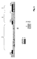
- FIG. 1 A TFA image sensor produced according to prior art
- FIG. 2 A TFA image sensor according to the invention after opening the CMOS passivation layer
- FIG. 3 The TFA image sensor according to FIG. 2 after back-etching the uppermost CMOS metallization
- FIG. 4 The TFA image sensor after applying the back electrodes of the photodiodes
- FIG. 5 The finished TFA image sensor based on the method according to the invention.
- FIG. 6 The TFA image sensor according to FIG. 5 with additional passivating transparent polymer layer;
- FIG. 7 The TFA image sensor according to FIG. 5 with additional color filter layers for passivation.
- a new metal layer 4 e.g., chromium
- the metal layer 4 can consist of chromium or another suitable metal.
- TFA image sensor involves the use of another passivating protective layer 10 , which, in addition to the peripheral electronics 9 , covers primarily the photodiode matrix 6 of the image sensor and passivates it against environmental influences. It can also be used in particular to protect the edge of the photodiode matrix 6 against environmental influences (e.g., penetrating moisture, which can increase the dark current).
- another passivating protective layer 10 which, in addition to the peripheral electronics 9 , covers primarily the photodiode matrix 6 of the image sensor and passivates it against environmental influences. It can also be used in particular to protect the edge of the photodiode matrix 6 against environmental influences (e.g., penetrating moisture, which can increase the dark current).
- This additional passivating protective layer 10 should exhibit a high transparency in the relevant spectral region, and lend itself to application in a low-temperature process (e.g., up to approx. 200° C. for amorphous silicon) so as not to impair the underlying structures.
- BCBs cyclotenes
- parylene or other polymeric transparent layers are suitable for this purpose.
- This passivating protective layer 10 must be structured in such a way as to expose only the bond pads 11 located in the area of the peripheral electronics 9 .
- the mosaic-structured color filter layers 8 normally used in color image sensors (e.g., Bayer pattern, U.S. Pat. No. 3,971,065), which also exert a passivating protective effect over the photodiode matrix 6 , are also provided at the edge of the photodiode matrix 6 and in the area of the peripheral electronics 9 of the image sensor.
- several color filter layers 8 can be stacked one on top of the other, thereby enabling a light screening of the switching components located in this area in addition to the passivation of peripheral electronics 9 .
- FIG. 2-7 only show the uppermost layers of the ASIC circuit 12 of relevance for the interface to the TFA layers of the TFA image sensor.
- FIG. 1 shows a cross section of a TFA image sensor according to prior art, i.e., without a passivation layer.
- the uppermost layer of the ASIC circuit 12 consists of an intermediate metal dielectric 13 , through which vias 14 extend in the pixel raster and connect the back electrodes 5 (metal 3 ) of the photodiode matrix 6 located on the ASIC circuit 12 with the contacts 15 (metal 1 ) of the ASIC circuit 12 .
- the photodiode matrix 6 is covered by the protective layer 10 .
- the peripheral electronics 9 required for operating the TFA image sensor are only shown diagrammatically.
- FIG. 1 shows one of numerous bond pads 11 (metal 2 ) in the peripheral region of the TFA image sensor for realizing external contacts. The bond pad 11 is connected with another contact 16 of the ASIC circuit through the intermediate metal dielectric 13 by means of vias.
- FIG. 2 shows an image sensor according to the invention after opening the CMOS passivation layer 1 (procedural step 1 per above list), FIG. 3 after back-etching the uppermost CMOS metallization 2 (metal 2 , procedural step 2 ), FIG. 4 after applying and structuring the back electrodes 5 (metal 3 ) of the photodiode matrix 6 (after procedural step 4 ).
- FIG. 5 presents a sketch of a complete image sensor realized in TFA technology.
- the other figures illustrate the TFA image sensors with passivating transparent protective layer 10 ( FIG. 6 ) or with the use of color filter layers 8 for passivation ( FIG. 7 ).
Abstract
Description
Claims (11)
Priority Applications (1)
| Application Number | Priority Date | Filing Date | Title |
|---|---|---|---|
| US11/271,492 US7326589B2 (en) | 2001-10-26 | 2005-11-11 | Method for producing a TFA image sensor and one such TFA image sensor |
Applications Claiming Priority (5)
| Application Number | Priority Date | Filing Date | Title |
|---|---|---|---|
| DE10152325 | 2001-10-26 | ||
| DE101523254.4 | 2001-10-26 | ||
| PCT/DE2002/003964 WO2003038901A1 (en) | 2001-10-26 | 2002-10-21 | Method for producing a tfa image sensor and one such tfa image sensor |
| US8239905A | 2005-03-10 | 2005-03-10 | |
| US11/271,492 US7326589B2 (en) | 2001-10-26 | 2005-11-11 | Method for producing a TFA image sensor and one such TFA image sensor |
Related Parent Applications (1)
| Application Number | Title | Priority Date | Filing Date |
|---|---|---|---|
| US8239905A Continuation | 2001-10-26 | 2005-03-10 |
Publications (2)
| Publication Number | Publication Date |
|---|---|
| US20060102829A1 US20060102829A1 (en) | 2006-05-18 |
| US7326589B2 true US7326589B2 (en) | 2008-02-05 |
Family
ID=7703474
Family Applications (1)
| Application Number | Title | Priority Date | Filing Date |
|---|---|---|---|
| US11/271,492 Expired - Lifetime US7326589B2 (en) | 2001-10-26 | 2005-11-11 | Method for producing a TFA image sensor and one such TFA image sensor |
Country Status (3)
| Country | Link |
|---|---|
| US (1) | US7326589B2 (en) |
| EP (1) | EP1438750A1 (en) |
| WO (1) | WO2003038901A1 (en) |
Cited By (2)
| Publication number | Priority date | Publication date | Assignee | Title |
|---|---|---|---|---|
| US20080128697A1 (en) * | 2002-07-16 | 2008-06-05 | Stmicroelectronics N.V. | Tfa image sensor with stability-optimized photodiode |
| US20130001597A1 (en) * | 2011-06-28 | 2013-01-03 | Osram Sylvania Inc. | Lighting Device Having a Color Tunable Wavelength Converter |
Families Citing this family (2)
| Publication number | Priority date | Publication date | Assignee | Title |
|---|---|---|---|---|
| DE102006046314A1 (en) * | 2006-09-29 | 2008-04-03 | Siemens Ag | Radiation direct converter module, has protecting layer made of parylene, which is provided partly on outer surface of metal layer and on radiation direct converter layer |
| US11589464B2 (en) * | 2020-12-22 | 2023-02-21 | Hamilton Sundstrand Corporation | Protective coating for electrical components and method of making the protective coating |
Citations (7)
| Publication number | Priority date | Publication date | Assignee | Title |
|---|---|---|---|---|
| US3971065A (en) | 1975-03-05 | 1976-07-20 | Eastman Kodak Company | Color imaging array |
| US4285007A (en) | 1979-02-26 | 1981-08-18 | Hitachi, Ltd. | Color solid-state imager and method of making the same |
| US6111247A (en) | 1997-12-08 | 2000-08-29 | Intel Corporation | Passivation protection of sensor devices having a color filter on non-sensor portion |
| EP1113499A2 (en) | 1999-12-28 | 2001-07-04 | Xerox Corporation | High fill factor image array having a continuous amorphous silicon sensor layer and a doped poly-silicon back contact |
| US6373117B1 (en) * | 1999-05-03 | 2002-04-16 | Agilent Technologies, Inc. | Stacked multiple photosensor structure including independent electrical connections to each photosensor |
| WO2002050921A1 (en) | 2000-12-21 | 2002-06-27 | Stmicroelectronics N.V. | Optoelectronic component for conversion of electromagnetic radiation into an intensity-dependent photocurrent |
| US6586812B1 (en) * | 1999-04-13 | 2003-07-01 | Agilent Technologies, Inc. | Isolation of alpha silicon diode sensors through ion implantation |
-
2002
- 2002-10-21 EP EP02782737A patent/EP1438750A1/en not_active Withdrawn
- 2002-10-21 WO PCT/DE2002/003964 patent/WO2003038901A1/en not_active Application Discontinuation
-
2005
- 2005-11-11 US US11/271,492 patent/US7326589B2/en not_active Expired - Lifetime
Patent Citations (7)
| Publication number | Priority date | Publication date | Assignee | Title |
|---|---|---|---|---|
| US3971065A (en) | 1975-03-05 | 1976-07-20 | Eastman Kodak Company | Color imaging array |
| US4285007A (en) | 1979-02-26 | 1981-08-18 | Hitachi, Ltd. | Color solid-state imager and method of making the same |
| US6111247A (en) | 1997-12-08 | 2000-08-29 | Intel Corporation | Passivation protection of sensor devices having a color filter on non-sensor portion |
| US6586812B1 (en) * | 1999-04-13 | 2003-07-01 | Agilent Technologies, Inc. | Isolation of alpha silicon diode sensors through ion implantation |
| US6373117B1 (en) * | 1999-05-03 | 2002-04-16 | Agilent Technologies, Inc. | Stacked multiple photosensor structure including independent electrical connections to each photosensor |
| EP1113499A2 (en) | 1999-12-28 | 2001-07-04 | Xerox Corporation | High fill factor image array having a continuous amorphous silicon sensor layer and a doped poly-silicon back contact |
| WO2002050921A1 (en) | 2000-12-21 | 2002-06-27 | Stmicroelectronics N.V. | Optoelectronic component for conversion of electromagnetic radiation into an intensity-dependent photocurrent |
Non-Patent Citations (6)
| Title |
|---|
| International Search Report from International application No. PCT/DE02/03964, filed Oct. 10, 2002. |
| International Search Report from International application No. PCT/DE02/04008, filed Oct. 24, 2002. |
| P. Rieve et al., a-Si:H Color Imagers and Colorimetry, Journal of Non-Crystalline Solids, vol. 266 to 269, pp. 1168 to 1172, (2000). |
| Schneider et al., Image Sensors In TFA (Thin Film on ASIC) Technology, Handbook of Computer Vision and Applications pp. 237 to 270, Academic Press, San Diego, 1999. |
| Schulte et al., Intelligent Image Sensor For On-Chip Contour Extraction, Proceedings of the SPIE, SPIE, Bellingham, VA, vol. 2247, Jun. 22, 1994, pp. 292-300, XP002080272. |
| Theil et al., Hydrogenated Amorphous Silicon Photodiode Technology for Advanced CMOS Active Pixel Sensor Imagers, Mat. Res. Soc. Symp. vol. 609, 2000 Materials Research Society pp. A14.31-A14.36. |
Cited By (3)
| Publication number | Priority date | Publication date | Assignee | Title |
|---|---|---|---|---|
| US20080128697A1 (en) * | 2002-07-16 | 2008-06-05 | Stmicroelectronics N.V. | Tfa image sensor with stability-optimized photodiode |
| US7701023B2 (en) * | 2002-07-16 | 2010-04-20 | Stmicroelectronics N.V. | TFA image sensor with stability-optimized photodiode |
| US20130001597A1 (en) * | 2011-06-28 | 2013-01-03 | Osram Sylvania Inc. | Lighting Device Having a Color Tunable Wavelength Converter |
Also Published As
| Publication number | Publication date |
|---|---|
| WO2003038901A1 (en) | 2003-05-08 |
| US20060102829A1 (en) | 2006-05-18 |
| EP1438750A1 (en) | 2004-07-21 |
Similar Documents
| Publication | Publication Date | Title |
|---|---|---|
| US7701023B2 (en) | TFA image sensor with stability-optimized photodiode | |
| US7382011B2 (en) | Solid-state image sensing device equipped with inner lens | |
| US6379979B1 (en) | Method of making infrared and visible light detector | |
| US6352876B1 (en) | Integrated semiconductor optic sensor device and corresponding manufacturing process | |
| US8963272B2 (en) | Photoelectric converter having chalcopyrite compound semiconductor layer partitioned into pixels and shielding layer arranged around each pixel | |
| EP1414077A2 (en) | Method for making and packaging image sensor die using protective coating | |
| US8242548B2 (en) | Solid-state imaging device, manufacturing method for the same, and imaging apparatus | |
| US20110228150A1 (en) | Photoelectric conversion film stack-type solid-state imaging device and imaging apparatus | |
| US7326589B2 (en) | Method for producing a TFA image sensor and one such TFA image sensor | |
| US20170117318A1 (en) | Rear-face illuminated solid state image sensors | |
| US8659687B2 (en) | Photoelectric conversion film stack-type solid-state imaging device and imaging apparatus | |
| JP2011171328A (en) | Solid-state image pickup element and method of manufacturing the same | |
| US7282382B2 (en) | Method for producing a photodiode contact for a TFA image sensor | |
| EP1344259B1 (en) | Optoelectronic component for conversion of electromagnetic radiation into an intensity-dependent photocurrent | |
| US7382034B2 (en) | Optoelectronic component having a conductive contact structure | |
| US10672811B2 (en) | Image sensing device | |
| EP1414074A2 (en) | Image sensor having reduced stress color filters and method of making | |
| US10998371B1 (en) | Film-based image sensor with suppressed light reflection and flare artifact | |
| JPH02166769A (en) | Laminated solid state image sensor and manufacture thereof | |
| EP1414076A2 (en) | Method of forming planar color filters in an image sensor | |
| JP7357262B2 (en) | Imaging device | |
| JP2014120629A (en) | Photoelectric conversion device and method of manufacturing the same | |
| EP4145514A1 (en) | Solid-state image sensor | |
| JP4090221B2 (en) | Solid-state imaging device and manufacturing method thereof | |
| EP1440476B1 (en) | Method for producing a photodiode contact for a tfa image sensor |
Legal Events
| Date | Code | Title | Description |
|---|---|---|---|
| AS | Assignment |
Owner name: STMICROELECTRONICS NV, NETHERLANDS Free format text: ASSIGNMENT OF ASSIGNORS INTEREST;ASSIGNORS:RIEVE, PETER;SEIBEL, KONSTANTIN;PRIMA, JENS;AND OTHERS;REEL/FRAME:017834/0251;SIGNING DATES FROM 20050826 TO 20051026 |
|
| STCF | Information on status: patent grant |
Free format text: PATENTED CASE |
|
| FPAY | Fee payment |
Year of fee payment: 4 |
|
| FPAY | Fee payment |
Year of fee payment: 8 |
|
| MAFP | Maintenance fee payment |
Free format text: PAYMENT OF MAINTENANCE FEE, 12TH YEAR, LARGE ENTITY (ORIGINAL EVENT CODE: M1553); ENTITY STATUS OF PATENT OWNER: LARGE ENTITY Year of fee payment: 12 |