US6369869B2 - Optical component and method of manufacture - Google Patents
Optical component and method of manufacture Download PDFInfo
- Publication number
- US6369869B2 US6369869B2 US09/779,611 US77961101A US6369869B2 US 6369869 B2 US6369869 B2 US 6369869B2 US 77961101 A US77961101 A US 77961101A US 6369869 B2 US6369869 B2 US 6369869B2
- Authority
- US
- United States
- Prior art keywords
- layer
- optical component
- orientating
- component according
- optical
- Prior art date
- Legal status (The legal status is an assumption and is not a legal conclusion. Google has not performed a legal analysis and makes no representation as to the accuracy of the status listed.)
- Expired - Lifetime
Links
- BFPQSQCXMUWCLV-UHFFFAOYSA-N C=CC(=O)OCCCCCCOC1=CC=C(C(=O)OC2=CC(C(=O)OCCCCC)=C(OC(=O)C3=CC=C(OCCCCCCOC(=O)C=C)C=C3)C=C2)C=C1.C=CC(=O)OCCCCCCOC1=CC=C(C(=O)OC2=CC(C)=C(OC(=O)C3=CC=C(OCCCCCCOC(=O)C=C)C=C3)C=C2)C=C1.C=CC(=O)OCCCCCCOC1=CC=C(C(=O)OC2=CC(Cl)=C(OC(=O)C3=CC=C(OCCCCCCOC(=O)C=C)C=C3)C=C2)C=C1 Chemical compound C=CC(=O)OCCCCCCOC1=CC=C(C(=O)OC2=CC(C(=O)OCCCCC)=C(OC(=O)C3=CC=C(OCCCCCCOC(=O)C=C)C=C3)C=C2)C=C1.C=CC(=O)OCCCCCCOC1=CC=C(C(=O)OC2=CC(C)=C(OC(=O)C3=CC=C(OCCCCCCOC(=O)C=C)C=C3)C=C2)C=C1.C=CC(=O)OCCCCCCOC1=CC=C(C(=O)OC2=CC(Cl)=C(OC(=O)C3=CC=C(OCCCCCCOC(=O)C=C)C=C3)C=C2)C=C1 BFPQSQCXMUWCLV-UHFFFAOYSA-N 0.000 description 1
- WJEHKDBYVDVFJO-OVCLIPMQSA-N C=NC1=CC=C(C2=CC=C(/C=C/C(=O)OCCOC(=O)C(C)(C)CC)C=C2)C=C1 Chemical compound C=NC1=CC=C(C2=CC=C(/C=C/C(=O)OCCOC(=O)C(C)(C)CC)C=C2)C=C1 WJEHKDBYVDVFJO-OVCLIPMQSA-N 0.000 description 1
- PLYPLAUCKLLNLL-UHFFFAOYSA-N CC1=CC=C(OC2=CC(N)=C3C(=C2N)C(=O)=C2C(N)=C(OC4=CC=C(C)C=C4)C=C(N)C2=C3=O)C=C1 Chemical compound CC1=CC=C(OC2=CC(N)=C3C(=C2N)C(=O)=C2C(N)=C(OC4=CC=C(C)C=C4)C=C(N)C2=C3=O)C=C1 PLYPLAUCKLLNLL-UHFFFAOYSA-N 0.000 description 1
Images


Classifications
-
- C—CHEMISTRY; METALLURGY
- C08—ORGANIC MACROMOLECULAR COMPOUNDS; THEIR PREPARATION OR CHEMICAL WORKING-UP; COMPOSITIONS BASED THEREON
- C08F—MACROMOLECULAR COMPOUNDS OBTAINED BY REACTIONS ONLY INVOLVING CARBON-TO-CARBON UNSATURATED BONDS
- C08F246/00—Copolymers in which the nature of only the monomers in minority is defined
-
- C—CHEMISTRY; METALLURGY
- C08—ORGANIC MACROMOLECULAR COMPOUNDS; THEIR PREPARATION OR CHEMICAL WORKING-UP; COMPOSITIONS BASED THEREON
- C08G—MACROMOLECULAR COMPOUNDS OBTAINED OTHERWISE THAN BY REACTIONS ONLY INVOLVING UNSATURATED CARBON-TO-CARBON BONDS
- C08G77/00—Macromolecular compounds obtained by reactions forming a linkage containing silicon with or without sulfur, nitrogen, oxygen or carbon in the main chain of the macromolecule
- C08G77/04—Polysiloxanes
- C08G77/38—Polysiloxanes modified by chemical after-treatment
-
- G—PHYSICS
- G02—OPTICS
- G02B—OPTICAL ELEMENTS, SYSTEMS OR APPARATUS
- G02B5/00—Optical elements other than lenses
- G02B5/30—Polarising elements
- G02B5/3016—Polarising elements involving passive liquid crystal elements
-
- G—PHYSICS
- G02—OPTICS
- G02F—OPTICAL DEVICES OR ARRANGEMENTS FOR THE CONTROL OF LIGHT BY MODIFICATION OF THE OPTICAL PROPERTIES OF THE MEDIA OF THE ELEMENTS INVOLVED THEREIN; NON-LINEAR OPTICS; FREQUENCY-CHANGING OF LIGHT; OPTICAL LOGIC ELEMENTS; OPTICAL ANALOGUE/DIGITAL CONVERTERS
- G02F1/00—Devices or arrangements for the control of the intensity, colour, phase, polarisation or direction of light arriving from an independent light source, e.g. switching, gating or modulating; Non-linear optics
- G02F1/01—Devices or arrangements for the control of the intensity, colour, phase, polarisation or direction of light arriving from an independent light source, e.g. switching, gating or modulating; Non-linear optics for the control of the intensity, phase, polarisation or colour
- G02F1/13—Devices or arrangements for the control of the intensity, colour, phase, polarisation or direction of light arriving from an independent light source, e.g. switching, gating or modulating; Non-linear optics for the control of the intensity, phase, polarisation or colour based on liquid crystals, e.g. single liquid crystal display cells
- G02F1/133—Constructional arrangements; Operation of liquid crystal cells; Circuit arrangements
- G02F1/1333—Constructional arrangements; Manufacturing methods
- G02F1/133365—Cells in which the active layer comprises a liquid crystalline polymer
-
- G—PHYSICS
- G02—OPTICS
- G02F—OPTICAL DEVICES OR ARRANGEMENTS FOR THE CONTROL OF LIGHT BY MODIFICATION OF THE OPTICAL PROPERTIES OF THE MEDIA OF THE ELEMENTS INVOLVED THEREIN; NON-LINEAR OPTICS; FREQUENCY-CHANGING OF LIGHT; OPTICAL LOGIC ELEMENTS; OPTICAL ANALOGUE/DIGITAL CONVERTERS
- G02F1/00—Devices or arrangements for the control of the intensity, colour, phase, polarisation or direction of light arriving from an independent light source, e.g. switching, gating or modulating; Non-linear optics
- G02F1/01—Devices or arrangements for the control of the intensity, colour, phase, polarisation or direction of light arriving from an independent light source, e.g. switching, gating or modulating; Non-linear optics for the control of the intensity, phase, polarisation or colour
- G02F1/13—Devices or arrangements for the control of the intensity, colour, phase, polarisation or direction of light arriving from an independent light source, e.g. switching, gating or modulating; Non-linear optics for the control of the intensity, phase, polarisation or colour based on liquid crystals, e.g. single liquid crystal display cells
- G02F1/133—Constructional arrangements; Operation of liquid crystal cells; Circuit arrangements
- G02F1/1333—Constructional arrangements; Manufacturing methods
- G02F1/1335—Structural association of cells with optical devices, e.g. polarisers or reflectors
- G02F1/13363—Birefringent elements, e.g. for optical compensation
- G02F1/133636—Birefringent elements, e.g. for optical compensation with twisted orientation, e.g. comprising helically oriented LC-molecules or a plurality of twisted birefringent sublayers
-
- G—PHYSICS
- G02—OPTICS
- G02F—OPTICAL DEVICES OR ARRANGEMENTS FOR THE CONTROL OF LIGHT BY MODIFICATION OF THE OPTICAL PROPERTIES OF THE MEDIA OF THE ELEMENTS INVOLVED THEREIN; NON-LINEAR OPTICS; FREQUENCY-CHANGING OF LIGHT; OPTICAL LOGIC ELEMENTS; OPTICAL ANALOGUE/DIGITAL CONVERTERS
- G02F1/00—Devices or arrangements for the control of the intensity, colour, phase, polarisation or direction of light arriving from an independent light source, e.g. switching, gating or modulating; Non-linear optics
- G02F1/01—Devices or arrangements for the control of the intensity, colour, phase, polarisation or direction of light arriving from an independent light source, e.g. switching, gating or modulating; Non-linear optics for the control of the intensity, phase, polarisation or colour
- G02F1/13—Devices or arrangements for the control of the intensity, colour, phase, polarisation or direction of light arriving from an independent light source, e.g. switching, gating or modulating; Non-linear optics for the control of the intensity, phase, polarisation or colour based on liquid crystals, e.g. single liquid crystal display cells
- G02F1/133—Constructional arrangements; Operation of liquid crystal cells; Circuit arrangements
- G02F1/1333—Constructional arrangements; Manufacturing methods
- G02F1/1337—Surface-induced orientation of the liquid crystal molecules, e.g. by alignment layers
- G02F1/133711—Surface-induced orientation of the liquid crystal molecules, e.g. by alignment layers by organic films, e.g. polymeric films
-
- G—PHYSICS
- G02—OPTICS
- G02F—OPTICAL DEVICES OR ARRANGEMENTS FOR THE CONTROL OF LIGHT BY MODIFICATION OF THE OPTICAL PROPERTIES OF THE MEDIA OF THE ELEMENTS INVOLVED THEREIN; NON-LINEAR OPTICS; FREQUENCY-CHANGING OF LIGHT; OPTICAL LOGIC ELEMENTS; OPTICAL ANALOGUE/DIGITAL CONVERTERS
- G02F1/00—Devices or arrangements for the control of the intensity, colour, phase, polarisation or direction of light arriving from an independent light source, e.g. switching, gating or modulating; Non-linear optics
- G02F1/01—Devices or arrangements for the control of the intensity, colour, phase, polarisation or direction of light arriving from an independent light source, e.g. switching, gating or modulating; Non-linear optics for the control of the intensity, phase, polarisation or colour
- G02F1/13—Devices or arrangements for the control of the intensity, colour, phase, polarisation or direction of light arriving from an independent light source, e.g. switching, gating or modulating; Non-linear optics for the control of the intensity, phase, polarisation or colour based on liquid crystals, e.g. single liquid crystal display cells
- G02F1/133—Constructional arrangements; Operation of liquid crystal cells; Circuit arrangements
- G02F1/1333—Constructional arrangements; Manufacturing methods
- G02F1/1337—Surface-induced orientation of the liquid crystal molecules, e.g. by alignment layers
- G02F1/133753—Surface-induced orientation of the liquid crystal molecules, e.g. by alignment layers with different alignment orientations or pretilt angles on a same surface, e.g. for grey scale or improved viewing angle
-
- G—PHYSICS
- G02—OPTICS
- G02F—OPTICAL DEVICES OR ARRANGEMENTS FOR THE CONTROL OF LIGHT BY MODIFICATION OF THE OPTICAL PROPERTIES OF THE MEDIA OF THE ELEMENTS INVOLVED THEREIN; NON-LINEAR OPTICS; FREQUENCY-CHANGING OF LIGHT; OPTICAL LOGIC ELEMENTS; OPTICAL ANALOGUE/DIGITAL CONVERTERS
- G02F1/00—Devices or arrangements for the control of the intensity, colour, phase, polarisation or direction of light arriving from an independent light source, e.g. switching, gating or modulating; Non-linear optics
- G02F1/01—Devices or arrangements for the control of the intensity, colour, phase, polarisation or direction of light arriving from an independent light source, e.g. switching, gating or modulating; Non-linear optics for the control of the intensity, phase, polarisation or colour
- G02F1/13—Devices or arrangements for the control of the intensity, colour, phase, polarisation or direction of light arriving from an independent light source, e.g. switching, gating or modulating; Non-linear optics for the control of the intensity, phase, polarisation or colour based on liquid crystals, e.g. single liquid crystal display cells
- G02F1/133—Constructional arrangements; Operation of liquid crystal cells; Circuit arrangements
- G02F1/1333—Constructional arrangements; Manufacturing methods
- G02F1/1337—Surface-induced orientation of the liquid crystal molecules, e.g. by alignment layers
- G02F1/133765—Surface-induced orientation of the liquid crystal molecules, e.g. by alignment layers without a surface treatment
-
- G—PHYSICS
- G02—OPTICS
- G02F—OPTICAL DEVICES OR ARRANGEMENTS FOR THE CONTROL OF LIGHT BY MODIFICATION OF THE OPTICAL PROPERTIES OF THE MEDIA OF THE ELEMENTS INVOLVED THEREIN; NON-LINEAR OPTICS; FREQUENCY-CHANGING OF LIGHT; OPTICAL LOGIC ELEMENTS; OPTICAL ANALOGUE/DIGITAL CONVERTERS
- G02F1/00—Devices or arrangements for the control of the intensity, colour, phase, polarisation or direction of light arriving from an independent light source, e.g. switching, gating or modulating; Non-linear optics
- G02F1/01—Devices or arrangements for the control of the intensity, colour, phase, polarisation or direction of light arriving from an independent light source, e.g. switching, gating or modulating; Non-linear optics for the control of the intensity, phase, polarisation or colour
- G02F1/13—Devices or arrangements for the control of the intensity, colour, phase, polarisation or direction of light arriving from an independent light source, e.g. switching, gating or modulating; Non-linear optics for the control of the intensity, phase, polarisation or colour based on liquid crystals, e.g. single liquid crystal display cells
- G02F1/133—Constructional arrangements; Operation of liquid crystal cells; Circuit arrangements
- G02F1/1333—Constructional arrangements; Manufacturing methods
- G02F1/1337—Surface-induced orientation of the liquid crystal molecules, e.g. by alignment layers
- G02F1/13378—Surface-induced orientation of the liquid crystal molecules, e.g. by alignment layers by treatment of the surface, e.g. embossing, rubbing or light irradiation
- G02F1/133788—Surface-induced orientation of the liquid crystal molecules, e.g. by alignment layers by treatment of the surface, e.g. embossing, rubbing or light irradiation by light irradiation, e.g. linearly polarised light photo-polymerisation
Definitions
- the invention is concerned with the manufacture of an anisotropic layer of cross-linked liquid crystalline monomers (LCP) in contact with an orientating layer on a single substrate, and with optical components having a layered structure comprising an orientating layer, a LCP layer, and at least one additional orientating layer over the LCP layer on a single substrate and their preferred use.
- LCP liquid crystalline monomers
- Anisotropic transparent or colored cross-linked polymer layers with three-dimensional orientation of the optical axis, either uniform or preset at individual places, are of great interest in many sectors of display technology, integrated optics, etc.
- Layer structures of liquid crystalline polymers are known, see EP-A-331 233. They are manufactured by orientating a monomer layer in a cell with a voltage applied to the cell plates and then irradiating in a partial region through a mask. By so doing, cross-linking is initiated in the irradiated region only. Subsequently, the direction of the external field is changed and the monomer regions which have not yet been cross-linked are re-orientated with respect to the new field direction. Thereupon, the latter region is also illuminated and thus cross-linked. Clearly, this method cannot yield an orientating structure with high local resolution, since the radical cross-linking reaction, owing to the shading of the mask, does not have sharp boundaries. Further, this method is invariably limited to the use of sandwich cells for orientating the layer structure in an electric field.
- optical strongly anisotropic layers consisting of orientated liquid crystal polymers in cells is also known from Research Disclosure No. 337, May 1992, Emsworth, GB, pages 410-411. There, the manufacture of such layers by placing the liquid crystal monomer in the cell, orientating by means of the two cell walls via rubbed polyimide surfaces of the cell and subsequent conventional photopolymerization in the cell is described. Further, it is mentioned that one of the two glass plates can be removed after the polymerization step in order to thereby obtain a single glass substrate coated with LC polymer. This orientated substrate can, moreover, be provided with a polyimide layer having a new direction of orientation (by rubbing).
- optical retarder layers are required on a single substrate, the manufacture requires, as described in Shannon et al., dismantling the cell. In so doing, the retarder layer must not be damaged. This complicates the manufacturing process rendering it impractical, especially in the case of large substrate areas as are required for high-information computers and TV-LCDs.
- Layer structures comprising a film of cross-linked liquid crystalline monomers in contact with an orientating layer of a photo-orientable polymer network (PPN) are described in European Application No. 0 611 981, published Aug. 24, 1994. The manufacture of these layer structures is effected by planar orientation of the liquid crystalline monomers by interaction with the PPN layer and fixing the orientation in a subsequent cross-linking step.
- Cross-linked liquid crystalline monomers are also referred to as LCPs (liquid crystal polymers) in the following text.
- liquid crystalline monomer layers can also be applied to and cross-linked on single substrate surfaces which already contain a LCP layer.
- a further orientating counter-substrate of a sandwich cell is required nor are magnetic fields or electric fields necessary for the orientation.
- EP-A-0 397 263 in which magnetic field orientation of dichroic dyes in a single LC monomer layer for the manufacture of a polarizing film is indicated as being preferred and is actually the sole exemplified process (field-free orientation is, indeed, claimed, but not demonstrated).
- the present invention provides and opens up new possibilities for optical and electro-optical components and devices using layer structures of the aforementioned kind.
- the invention provides a process for making an isotropic layer of cross-linked liquid crystalline monomers in contact with an orientating layer on a single substrate.
- This process comprises applying an orientating layer onto a single substrate, then applying a layer of a non-cross-linked liquid crystalline monomer, and subsequently cross-linking the monomer.
- an optical component having a layer structure.
- the component comprises a substrate, a first orientating layer, a liquid crystalline monomer layer, and a second orientating layer.
- the first and second orientating layers are located on opposite sides of the crystalline monomer layer. At least one of the orientating layers includes a photo-orientating polymer network.
- the manufacture in accordance with the invention of an anisotropic layer of cross-linked liquid crystalline monomers (LCP) in contact with an orientating layer comprises applying an orientating layer on a single substrate and applying to this a layer of a non-cross- linked liquid crystalline monomer and subsequently cross-linking the monomer.
- additional orientating and liquid crystal layers can be applied in further steps and these layers can be cross-linked.
- optically isotropic de-coupling layers or electrically conducting layers can be inserted or applied between individual LCP layers under the following orientating layers.
- the optical component according to the invention is characterized in that at least one of the orientating layers is a layer of a photo-orientating polymer network (PPN) or has a local varying orientating pattern.
- PPN photo-orientating polymer network
- nematic, cholesteric, ferroelectric or non-linear optical (NLO) activity at room temperature Preferably, use is made of monomer mixtures which have nematic, cholesteric, ferroelectric or non-linear optical (NLO) activity at room temperature.
- NLO non-linear optical
- the second and other LCP layers can also be applied directly, i.e. without intermediate PPN layers, to the first.LCP layer and subsequently cross-linked. Thereby, the monomers in the second and subsequent layers take over the preferred orientation of the first or respective underlying LCP layers.
- the PPN and LCP layers need not cover the entire surface of the substrate, but can cover all or part of the surface in individual and varying manner.
- multi-layer structures are used in optical and electro-optical devices, particularly in the manufacture of liquid crystal cells in which the various LCP layers serve different optical and orientating purposes. They are also used in integrated optical devices, e.g. in strip waveguides, Mach-Zender interferometers and frequency-doubling waveguide arrangements. Finally, these layer structures can be used as a safeguard against counterfeiting and copying.
- FIG. 1 shows a layer structure of an optical component according to the invention
- FIG. 2 shows a layer structure of an optical component with an additional layer
- FIG. 3 shows an alternative layer structure with an additional de-coupling layer
- FIG. 4 shows another layer structure with locally varying orientation of component regions
- FIG. 5 shows another layer structure as in FIG. 4, but with an additional de-coupling layer
- FIG. 6 shows a supertwisted nematic (STN) liquid crystal display cell with a layer structure according to FIG. 3;
- FIG. 7 shows a diagram of the directions of the nematic director, the optical retarder layer and the polarizers in the cell according to FIG. 6;
- FIG. 8 shows an alternative liquid crystal cell with a layer structure according to FIG. 2, but with an additional ITO layer.
- the invention provides a process for making an isotropic layer of cross-linked liquid crystalline monomers in contact with an orientating layer on a single substrate.
- This process comprises applying an orientating layer onto a single substrate, then applying a layer of a non-cross-linked liquid crystalline monomer, and subsequently cross-linking the monomer.
- an optical component having a layer structure.
- the component comprises a substrate, a first orientating layer, a liquid crystalline monomer layer, and a second orientating layer.
- the first and second orientating layers are located on opposite sides of the crystalline monomer layer. At least one of the orientating layers includes a photo-orientating polymer network.
- FIG. 1 is a diagrammatic section through a layer structure in one embodiment of the invention, showing a substrate 1 of transparent or reflecting material such as glass, polymer, metal, paper, etc.
- a layer 2 of a photo-orientated polymer network is disposed on the substrate and either covers the entire substrate uniformly or has varying local planar orientation.
- the layer can be made, for example, of cinnamic acid derivatives which are described and published in European Patent Applications Nos. 0 525 477 and 0 525 478.
- the layer is orientated and simultaneously cross-linked by selective irradiation with linear polarized UV light.
- the layer 2 can also be a conventional orientating layer, for example a polyimide layer rubbed in one direction or a layer having an orientating effect and obtained by oblique sputtering with SiO x .
- the orientating layer will usually have uniform orientation over the entire substrate surface. In applications where uniform orientation over the entire surface is desired, this mechanical alternative may be less expensive to manufacture than a PPN layer.
- the PPN layer 2 can, in turn, be applied to a conventionally orientated layer previously deposited on the substrate 1 , e.g. an obliquely sputtered SiO x layer or a uniformly rubbed polymer layer.
- the layer 2 is adjacent an anisotropic layer 3 of orientated cross-linked liquid crystal monomers.
- the layer 3 has an arrangement of molecules having an orientation determined by the orientation of the underlying layer 2 or transferred therefrom to the liquid crystal layer.
- the LCP layer 3 is photo cross-linked by the action of light of suitable wavelength and retains the orientation of molecules predetermined by the layer 2 .
- the photo cross-linking fixes the orientation of the LCP layer 3 so that it is unaffected by extreme external influences such as light or high temperatures. Even optical or thermal instabilities occurring in the course of time in the PPN layer 2 will not adversely influence the orientating properties of the LCP layer 3 after cross-linking.
- the LCP layer 3 is adjacent another orientating layer which, as before, is either a PPN layer or a conventional orientating layer depending on whether locally varying orientation patterns or a uniform orientation for an adjacent second LCP layer 5 according to FIG. 2 is desired.
- the LCP layer 5 is produced in the same manner and has the same properties as the layer 3 , but the two LCP layers are usually differently orientated.
- FIG. 3 shows an embodiment of a component in which, as in the previously described case, two LCP layers with respective orientation layers are disposed on a substrate 1 .
- an optically isotropic or weakly anisotropic de-coupling layer 6 is disposed between the lower LCP layer 3 and the upper orientating layer 4 to prevent the LCP layer 3 exerting an orientating influence, which it of course also can have as a retarder layer, on the, upper hybrid layers 4 , 5 and consequently on a liquid crystal disposed above the layer 5 .
- the de-coupling layer 6 can be made, for example, of silicon oxides (SiO x ) or isotropic polymers such as polyvinyl alcohol (PVA) or nylon.
- FIG. 4 shows a layer structure which, like FIG. 2, consists of four layers superposed on a substrate 1 , i.e. a first PPN layer 2 , a first LCP layer 3 , an additional PPN layer and an additional LCP layer.
- a substrate 1 i.e. a first PPN layer 2 , a first LCP layer 3 , an additional PPN layer and an additional LCP layer.
- the two upper layers have different local orientations.
- the PPN layer has regions 7 with a first orientation and regions 8 with a second orientation different from the first. Since the orientation is transmitted to the LCP layer before cross-linking thereof, the LCP layer has regions 9 with the first orientation and regions 10 with the second orientation.
- the layer structure shown in FIG. 5 corresponds to that of FIG. 3, i.e. with a decoupling layer, except that the upper PPN layer as before contains differently oriented regions 7 and 8 and the upper LCP layer contains regions 9 and 10 with correspondingly different orientation.
- the layer 3 can serve as a retarder and layer 5 or 9 , 10 can serve as the orientating layer for the liquid crystal.
- the optical path difference of the LCP layer 3 is usually given a high value, i.e. above 100 nm.
- FIG. 6 is a diagrammatic section through a liquid crystal cell constructed using a layer structure of this kind.
- a liquid crystal layer 15 lies between two glass plates 1 and 12 coated with a number of layers on their surfaces facing the liquid crystal.
- the plate 1 is firstly provided with an electrode layer 11 , preferably of indium tin oxide (ITO) for applying a voltage.
- ITO indium tin oxide
- the ITO layer 11 may alternatively be applied over the layer 3 or 6 .
- the layer structure has the configuration shown in FIG. 3, i.e. two PPN-LCP combinations 2 , 3 and 4 , 5 with an alternately interposed de-coupling layer 6 .
- the LCP layer 3 serves as a retarder, whereas the LCP layer 5 orients the liquid crystal 15 .
- the substrate can also be provided with a reflective layer.
- the other glass plate 12 is likewise coated with an ITO electrode layer 13 underneath an orientation layer 14 , e.g. of unidirectionally ground PVA.
- FIG. 7 shows the arrangement of polarizers P 1 and P 2 , the direction of the slow optical axis c e of the optical retarder 3 , and the wall orientation directions ⁇ circumflex over (n) ⁇ i and ⁇ circumflex over (n) ⁇ 2 of the liquid crystal layer 15 adjacent the two orientation layers 5 and 14 .
- ⁇ circumflex over (n) ⁇ 1 and P 1 are on the retarder side.
- This cell is opaque when no voltage is applied, but becomes transparent when actuated with a suitable voltage. Because of the incorporated retarder 3 , the usual interference colors in STN cells do not occur, i.e. the cell is white as regards optical visibility.
- the retarder layer 3 can also consist of a liquid crystal mixed with chiral dopants.
- An angle of twist between 0° and 360° can be obtained by varying the concentration of dopant.
- the twisting can be levorotatory or dextrorotatory.
- Twisted retarders of this kind are particularly suitable for color compensation of STN display cells.
- a twisted optical retarder is used in the STN cell of FIG. 6, the following conditions must be met:
- the sense of rotation of the optical retarder is opposite to the sense of rotation of the liquid crystal layer 15 , the angle of rotation ( ⁇ ) of the optical retarder being the same as that of the liquid crystal layer.
- the slow optical axis of the optical retarder on the side facing the liquid crystal, is at right angles to the orientation direction ⁇ circumflex over (n) ⁇ 1 of the liquid crystal 15 , and
- the optical path difference of the optical retarder is equal to the optical path difference of the liquid crystal layer 15 .
- a helically twisted retarder can be constructed if a multi-layer system of alternate successive orientation layers and LCP layers, optionally with interposition of de-coupling layers, is so constructed that the planar optical axes of the layers vary in azimuth, resulting in a helical structure.
- Layers with high twist serving as cholesteric optical filters, are obtained by increasing the concentration of chiral dopants in twisted retarder layers. Owing to the thermal stability of the layers, these filters can be used at temperatures far above 100° C.
- the wavelength of selective reflection of these cholesteric filters can be varied by varying the chiral dopants.
- the bandwidth of selective reflection of the filter combination can be varied by superposing at least two cholesteric layers, each with different selective reflection.
- Retarder or orientation layers with an integrated linear polarizer, or absorptive optical filters can be obtained by adding dichroic dyes, which are oriented by the liquid crystal molecules in the LCP layer.
- the PPN material can comprise, for example, cinnamic acid-derivatives.
- a glass plate was spin-coated with a 5% solution of the PPN material in NMP at 2000 rpm for 1 minute.
- the layer was then dried at 130° C. for 2 hours on a heating bench and for a further 4 hours at 130° C. in vacuo.
- the layer was then illuminated with the linear polarized light from a 200 W Hg very high pressure lamp at room temperature for 5 minutes.
- the layer could then be used as an orientating layer for liquid crystals.
- the thermal stability of the orientation capacity is too low for many applications. For example the orientation capacity disappeared e.g. after 15 minutes at 120° C.
- the diacrylate monomers were present in the mixture in the following proportions:
- the M LCP mixture was then dissolved in anisole.
- the thickness of the LCP layer can be adjusted over a wide range by varying the concentration of M LCP in anisole.
- the layers, after orientation, were irradiated with isotropic light from a 150 W xenon lamp for about 30 minutes, thus fixing the orientation.
- a PPN-coated glass plate was irradiated with polarized UV light for 5 minutes.
- a 40% solution of M LCP in anisole was deposited by centrifuging on to the illuminated layer. Spin parameter: 2 minutes at 2000 rpm.
- the resulting cross-linkable LCP layer was orientated in accordance with the direction of polarization of the UV light. After cross-linking the LCP layer had a thickness of 2.2 ⁇ m.
- the coated glass plate is disposed under crossed polarizers so that the polarizers are parallel or at right angles to the direction of polarization during illumination of the PPN layer, the plate is dark. If, however, the plate is rotated through 45° in the plate plane, the plate becomes light, i.e. it has double refraction.
- the optical delay is about 300 nm.
- An isotropic SiO x de-coupling layer 50 nm thick was deposited by sputtering on to the hybrid layer with an optical delay of 300 nm.
- a PPN layer was then constructed on the de-coupling layer as described in Example 1.
- the PPN layer was divided into two regions illuminated in different directions of polarization, the direction of polarization of the light in one half being parallel to and in the other half at right angles to the optical axis of the underlying retarder layer. One half was covered during illumination of the other half. The result was two regions with directions of planar orientation at right angles to one another.
- a 5% solution of M LCP in anisole was prepared.
- the solution was deposited by centrifuging on to the locally variously illuminated PPN layer. Spin parameter: 2 minutes at 2000 rpm.
- the layer was then cooled at 0.1° C./min to a few degrees below the clearing point and then photochemically cross-linked.
- this hybrid substrate and a second ground PVA-coated substrate are used to construct an LC cell and the cell is filled with a liquid crystal, the result is a twisted cell (TN) configuration in one half of the cell and a homogeneous planar arrangement of the LC molecules in the other half.
- the hybrid substrate serves on the one hand as an optical retarder and on the other hand as an orientation layer for the liquid crystal.
- the optical axis of the retarder can be different from the direction in which the LC molecules are oriented.
- the multilayer layer is thermally and optically stable, as a result of the two cross-linked LCP layers.
- isotropic decoupling layers of nylon were made.
- 0.1% nylon was dissolved in trifluoroethanol and deposited by spin-coating on to the first LCP layer.
- a PPN layer was applied to an ITO-coated glass plate and irradiated with linear-polarized light.
- a 53% solution of M LCP in anisole was deposited by centrifugation and cross-linked (spin parameter: 2 minutes at 2000 rpm).
- the optical delay of this retarder layer was 530 nm.
- a second PPN layer was applied, de-coupled from the retarder by an isotropic SiO2 layer.
- the direction of the polarizer for illuminating the second PPN layer was rotated through 75° relatively to the direction of polarization of illumination of PPN1.
- a thin LCP layer was deposited on the PPN2 layer after illumination, as in Example 3.
- the second plate was disposed so that the angle between its direction of rubbing and the direction of orientation of the hybrid layer was 240°.
- the transmission directions of the two polarizers required were adjusted as in FIG. 7.
- the doped mixture was then dissolved to a 40% in anisole and centrifugally applied to an illuminated PPN layer (2 minutes at 2000 rpm). After cross-linking, the thickness of the LCP layer was about 2.2 ⁇ m.
- the coated plate is observed under crossed polarizers, the direction of transmission on the substrate side being parallel to the direction of polarization of the light illuminating the PPN, the layer does not appear dark as would be the case with a linear retarder. However, the layer is darkest when the analyzer is rotated through 30°. Accordingly, the plane of polarization of the linear polarized light is rotated through 30° in transit through the retarder, corresponding to the twist in the LCP layer.
- the twist can be adjusted between 0° and 360° by varying the concentration of the chiral dopant.
- a dextrorotatory chiral dopant can be used instead of a levorotatory dopant.
- These twisted retarders are also of interest e.g. for color compensation of STN displays.
- the first PPN-LCP layer combination can be a twisted retarder, thus further increasing the contrast. Consequently, the M LCP mixture for the first LCP layer was doped with a dextrorotatory chiral dopant.
- the spin parameters were so chosen that the optical delay of the LCP layer was equal to that of the liquid crystal 15 in FIG. 6 .
- the pitch of the LCP layer could then be adjusted via the concentration of dopant such that the angle of rotation of the retarder was equal to the angle of rotation of the liquid crystal.
- the orientation layer above the twisted retarder was illuminated such that its direction of orientation was at right angles to the slow axis of the retarder on the side facing the orientating layer. In a similar manner to Example 4, this substrate was used to construct an STN cell and filled with a levorotatory liquid crystal.
- Example 3 A 50% solution of M LCP in anisole was applied by centrifugation at room temperature on to a PPN layer irradiated with linear polarized light, and was cross-linked. The resulting optical retarder had a delay of 470 nm. Under cross-polarizers, the plate was orange-colored.
- a 50 nm thick isotropic decoupling layer of SiO x was deposited by sputtering, followed by a second PPN layer. Layer PPN2 was then divided into three regions, which were illuminated with different directions of polarization. The directions of polarization were parallel in region 1 , perpendicular in region 2 and 45° to the direction of polarization of the illumination of PPN1 in region 3 . During illumination of each region the other regions were covered.
- hybrid layer was disposed under cross-polarizers in such a manner that the direction of polarization of PPN1 illumination lay at 45° to the polarizers, three colors were recognized:
- optical delays of the two LCP layers are added in region 1 and substrate in region 2 .
- the illumination of the individual layers can also be effected by varying the polarization directions with angles between 0° and 90° compared with the first illumination.
- Lyot/Oehman or olc interference filters can also be realized, the transmission range of which being adjustable by the number of layers, their thickness and the direction of their optical axes.
- the transmission range can be variously adjusted pixel-wise by the structuring.
- the M LCP mixture was doped with 12% of the chiral levo-rotatory dopant in Example 5.
- the resulting cholesteric mixture had a pitch of about 360 nm.
- the doped mixture was dissolved to 40% in anisole, applied centrifugally to a PPN layer illuminated with linear polarized light and cross-linked.
- the width of the reflection bands was 70 nm.
Abstract
An optical component having a hybrid layer structure includes an orienting layer, a further layer in contact with the orienting layer and incorporating a cross-linked liquid crystalline monomer and at least one additional orienting layer on top of the liquid crystalline layer, and preferably includes one additional cross-linked liquid crystalline monomer. The layers have different functions, such as orienting or retarding. At least one of the orienting layers should be a photo-orientating polymer network layer, or have locally varying orienting pattern. These optical components are useful in transmittance and reflective liquid crystal displays, such as rotation cells, STN cells, ferroelectric cells, and cells having an addressable active matrix. Such cells are useful in optical and integrated optical devices, and may be used for safeguarding against counterfeiting and copying in transmission.
Description
This is a continuation of application Ser. No. 09/550,111, filed on Apr. 14, 2000 now abandoned (which is incorporated by reference herein), which is a continuation of application Ser. No. 08/721,509, filed on Sep. 26, 1996, now U.S. Pat. No. 6,160,597 where application Ser. No. 08/721,509 is a continuation of application Ser. No. 08/489,865, filed on Jun. 13, 1995, now abandoned and is also a continuation in part of application Ser. No. 08/194,234, filed on Feb. 10, 1994 now U.S. Pat. No. 5,602,661.
1. Field
The invention is concerned with the manufacture of an anisotropic layer of cross-linked liquid crystalline monomers (LCP) in contact with an orientating layer on a single substrate, and with optical components having a layered structure comprising an orientating layer, a LCP layer, and at least one additional orientating layer over the LCP layer on a single substrate and their preferred use.
2. Description
Anisotropic transparent or colored cross-linked polymer layers with three-dimensional orientation of the optical axis, either uniform or preset at individual places, are of great interest in many sectors of display technology, integrated optics, etc.
For some years, substances having this property have become known, namely certain cross-linkable liquid crystalline diacrylates and diepoxides. These substances as monomers, that is before cross-linking, can be orientated in the liquid crystalline phase in sandwich cells consisting of, for example, glass plates having an interposed monomer layer with the aid of conventional orientating layers on the two glass plate surfaces or under the influence of external fields, such as strong magnetic or electric fields. In a second phase, the monomer layer can be photo-cross-linked in the cells such that the wall forces acting on the two sides of the monomer layer, or the applied fields, preserve the preset orientation during the cross-linking process.
These external mechanical, electrical or magnetic forces prevent thermodynamic orientation relaxation inherent in liquid crystals and counteract the de-orientating forces of conventional cross-linking processes. In the absence of these external forces a de-orientation or a re-orientation of the liquid crystals usually takes place. The re-orientation from planar to perpendicular at the interface to the atmosphere opposite the substrate surface has been shown in the case of single substrates, see Hikmet and de Witz, J. Appl. Phy. 70:1265-1269 (1991). (Throughout the specification, documents have been identified. The contents of each of these documents are herein incorporated by reference).
Layer structures of liquid crystalline polymers are known, see EP-A-331 233. They are manufactured by orientating a monomer layer in a cell with a voltage applied to the cell plates and then irradiating in a partial region through a mask. By so doing, cross-linking is initiated in the irradiated region only. Subsequently, the direction of the external field is changed and the monomer regions which have not yet been cross-linked are re-orientated with respect to the new field direction. Thereupon, the latter region is also illuminated and thus cross-linked. Clearly, this method cannot yield an orientating structure with high local resolution, since the radical cross-linking reaction, owing to the shading of the mask, does not have sharp boundaries. Further, this method is invariably limited to the use of sandwich cells for orientating the layer structure in an electric field.
Recently, there have become known methods which permit the production of orientating layers with locally variable orientating properties. The orientation of dichroic dye molecules incorporated in the polymer with the aid of photolithographic methods is described in U.S. Pat. No. 4,974,941, the contents of which are herein incorporated by reference.
The orientability and photo-structurability of a liquid crystalline monomer layer in a sandwich cell, the two surfaces of which have been photo-orientated by the laser orientation process described in U.S. Pat. No. 4,974,941, has also recently become known. This process is also limited to orientation of the monomer layer in a cell. The orientation impressed by the cell surfaces is frozen by subsequent conventional photopolymerization of the liquid crystalline monomer layer in the cell. In order to obtain a coated single substrate, the cell must be dismantled after the polymerization (P. J. Shannon, W. M. Gibbons, S. T. Sun, Nature, 368:532 (1994)).
The production of optical strongly anisotropic layers consisting of orientated liquid crystal polymers in cells is also known from Research Disclosure No. 337, May 1992, Emsworth, GB, pages 410-411. There, the manufacture of such layers by placing the liquid crystal monomer in the cell, orientating by means of the two cell walls via rubbed polyimide surfaces of the cell and subsequent conventional photopolymerization in the cell is described. Further, it is mentioned that one of the two glass plates can be removed after the polymerization step in order to thereby obtain a single glass substrate coated with LC polymer. This orientated substrate can, moreover, be provided with a polyimide layer having a new direction of orientation (by rubbing).
After again assembling the thus-prepared polymer substrate in a second orientated sandwich cell, filling this cell with a further monomer layer and subsequent conventional photopolymerization, the optical pitch differences of the two differently oriented LC polymer layers in the cell are added or subtracted.
Since the rubbing of the polyimide layers on the cell surfaces is a macroscopic process, no orientation pattern can be produced with this process, the cells being uniformly orientated over the entire surface. Further, it is extremely time consuming and expensive for the manufacturer of cells having precise plate separations for the realization of uniform optical pitch differences (in the ten nanometer range).
Where, optical retarder layers are required on a single substrate, the manufacture requires, as described in Shannon et al., dismantling the cell. In so doing, the retarder layer must not be damaged. This complicates the manufacturing process rendering it impractical, especially in the case of large substrate areas as are required for high-information computers and TV-LCDs.
Layer structures comprising a film of cross-linked liquid crystalline monomers in contact with an orientating layer of a photo-orientable polymer network (PPN) are described in European Application No. 0 611 981, published Aug. 24, 1994. The manufacture of these layer structures is effected by planar orientation of the liquid crystalline monomers by interaction with the PPN layer and fixing the orientation in a subsequent cross-linking step. Cross-linked liquid crystalline monomers are also referred to as LCPs (liquid crystal polymers) in the following text.
It has now surprisingly been found that liquid crystalline monomer layers can also be applied to and cross-linked on single substrate surfaces which already contain a LCP layer. For this purpose, neither a further orientating counter-substrate of a sandwich cell is required nor are magnetic fields or electric fields necessary for the orientation. This contrasts with EP-A-0 397 263, in which magnetic field orientation of dichroic dyes in a single LC monomer layer for the manufacture of a polarizing film is indicated as being preferred and is actually the sole exemplified process (field-free orientation is, indeed, claimed, but not demonstrated).
Furthermore, it has surprisingly been found that the orientation of these monomer layers on a single substrate is not influenced or destroyed by subsequent polymerization or photo-cross linking. Thus, it is for the first time possible to manufacture on single LCP-orientated substrate surfaces in a simple sequential manner solid films consisting of several orientated liquid crystalline polymer layers. Further, additional layers having different optical and/or electrical functions can be integrated in these complex hybrid layers. This offers for the first time the possibility of realizing not only known but also novel optical components such as polarization-interference filters, optical retarders, polarizers, etc. on single substrates by means of LCPs and to combine and to integrate these components in hybrid layers. Further, additional functional layers such as orientating layers for liquid crystals can be integrated in the hybrid layers.
The present invention provides and opens up new possibilities for optical and electro-optical components and devices using layer structures of the aforementioned kind.
The invention provides a process for making an isotropic layer of cross-linked liquid crystalline monomers in contact with an orientating layer on a single substrate. This process comprises applying an orientating layer onto a single substrate, then applying a layer of a non-cross-linked liquid crystalline monomer, and subsequently cross-linking the monomer. Also provided is an optical component having a layer structure. The component comprises a substrate, a first orientating layer, a liquid crystalline monomer layer, and a second orientating layer. The first and second orientating layers are located on opposite sides of the crystalline monomer layer. At least one of the orientating layers includes a photo-orientating polymer network.
The manufacture in accordance with the invention of an anisotropic layer of cross-linked liquid crystalline monomers (LCP) in contact with an orientating layer comprises applying an orientating layer on a single substrate and applying to this a layer of a non-cross- linked liquid crystalline monomer and subsequently cross-linking the monomer. For the manufacture of more complex layer structures, additional orientating and liquid crystal layers can be applied in further steps and these layers can be cross-linked. Moreover, if desired, optically isotropic de-coupling layers or electrically conducting layers can be inserted or applied between individual LCP layers under the following orientating layers.
The optical component according to the invention is characterized in that at least one of the orientating layers is a layer of a photo-orientating polymer network (PPN) or has a local varying orientating pattern.
Preferably, use is made of monomer mixtures which have nematic, cholesteric, ferroelectric or non-linear optical (NLO) activity at room temperature.
The second and other LCP layers can also be applied directly, i.e. without intermediate PPN layers, to the first.LCP layer and subsequently cross-linked. Thereby, the monomers in the second and subsequent layers take over the preferred orientation of the first or respective underlying LCP layers.
It will be appreciated that the PPN and LCP layers need not cover the entire surface of the substrate, but can cover all or part of the surface in individual and varying manner.
These multi-layer structures are used in optical and electro-optical devices, particularly in the manufacture of liquid crystal cells in which the various LCP layers serve different optical and orientating purposes. They are also used in integrated optical devices, e.g. in strip waveguides, Mach-Zender interferometers and frequency-doubling waveguide arrangements. Finally, these layer structures can be used as a safeguard against counterfeiting and copying.
Embodiments of the invention will be described hereinafter with reference to the accompanying simplified diagrammatic drawings in which:
FIG. 1 shows a layer structure of an optical component according to the invention;
FIG. 2 shows a layer structure of an optical component with an additional layer;
FIG. 3 shows an alternative layer structure with an additional de-coupling layer;
FIG. 4 shows another layer structure with locally varying orientation of component regions;
FIG. 5 shows another layer structure as in FIG. 4, but with an additional de-coupling layer;
FIG. 6 shows a supertwisted nematic (STN) liquid crystal display cell with a layer structure according to FIG. 3;
FIG. 7 shows a diagram of the directions of the nematic director, the optical retarder layer and the polarizers in the cell according to FIG. 6; and
FIG. 8 shows an alternative liquid crystal cell with a layer structure according to FIG. 2, but with an additional ITO layer.
The subject invention will now be described in terms of its preferred embodiments. These embodiments are set forth to aid in understanding the invention, but are not to be construed as limiting.
The invention provides a process for making an isotropic layer of cross-linked liquid crystalline monomers in contact with an orientating layer on a single substrate. This process comprises applying an orientating layer onto a single substrate, then applying a layer of a non-cross-linked liquid crystalline monomer, and subsequently cross-linking the monomer. Also provided is an optical component having a layer structure. The component comprises a substrate, a first orientating layer, a liquid crystalline monomer layer, and a second orientating layer. The first and second orientating layers are located on opposite sides of the crystalline monomer layer. At least one of the orientating layers includes a photo-orientating polymer network.
FIG. 1 is a diagrammatic section through a layer structure in one embodiment of the invention, showing a substrate 1 of transparent or reflecting material such as glass, polymer, metal, paper, etc. A layer 2 of a photo-orientated polymer network is disposed on the substrate and either covers the entire substrate uniformly or has varying local planar orientation. The layer can be made, for example, of cinnamic acid derivatives which are described and published in European Patent Applications Nos. 0 525 477 and 0 525 478.
The layer is orientated and simultaneously cross-linked by selective irradiation with linear polarized UV light.
Instead of the PPN layer, the layer 2 can also be a conventional orientating layer, for example a polyimide layer rubbed in one direction or a layer having an orientating effect and obtained by oblique sputtering with SiOx. In this case, the orientating layer will usually have uniform orientation over the entire substrate surface. In applications where uniform orientation over the entire surface is desired, this mechanical alternative may be less expensive to manufacture than a PPN layer.
The PPN layer 2 can, in turn, be applied to a conventionally orientated layer previously deposited on the substrate 1, e.g. an obliquely sputtered SiOx layer or a uniformly rubbed polymer layer.
The layer 2 is adjacent an anisotropic layer 3 of orientated cross-linked liquid crystal monomers. The layer 3 has an arrangement of molecules having an orientation determined by the orientation of the underlying layer 2 or transferred therefrom to the liquid crystal layer. The LCP layer 3 is photo cross-linked by the action of light of suitable wavelength and retains the orientation of molecules predetermined by the layer 2. The photo cross-linking fixes the orientation of the LCP layer 3 so that it is unaffected by extreme external influences such as light or high temperatures. Even optical or thermal instabilities occurring in the course of time in the PPN layer 2 will not adversely influence the orientating properties of the LCP layer 3 after cross-linking.
The LCP layer 3 is adjacent another orientating layer which, as before, is either a PPN layer or a conventional orientating layer depending on whether locally varying orientation patterns or a uniform orientation for an adjacent second LCP layer 5 according to FIG. 2 is desired. The LCP layer 5 is produced in the same manner and has the same properties as the layer 3, but the two LCP layers are usually differently orientated.
FIG. 3 shows an embodiment of a component in which, as in the previously described case, two LCP layers with respective orientation layers are disposed on a substrate 1. In contrast to the embodiment in FIG. 2, however, an optically isotropic or weakly anisotropic de-coupling layer 6 is disposed between the lower LCP layer 3 and the upper orientating layer 4 to prevent the LCP layer 3 exerting an orientating influence, which it of course also can have as a retarder layer, on the, upper hybrid layers 4, 5 and consequently on a liquid crystal disposed above the layer 5. The de-coupling layer 6 can be made, for example, of silicon oxides (SiOx) or isotropic polymers such as polyvinyl alcohol (PVA) or nylon.
FIG. 4 shows a layer structure which, like FIG. 2, consists of four layers superposed on a substrate 1, i.e. a first PPN layer 2, a first LCP layer 3, an additional PPN layer and an additional LCP layer. In contrast to the arrangement according to FIG. 2, however, the two upper layers have different local orientations. The PPN layer has regions 7 with a first orientation and regions 8 with a second orientation different from the first. Since the orientation is transmitted to the LCP layer before cross-linking thereof, the LCP layer has regions 9 with the first orientation and regions 10 with the second orientation.
Similarly, the layer structure shown in FIG. 5 corresponds to that of FIG. 3, i.e. with a decoupling layer, except that the upper PPN layer as before contains differently oriented regions 7 and 8 and the upper LCP layer contains regions 9 and 10 with correspondingly different orientation.
When a layer structure shown in FIGS. 1-5 and with two individually oriented LCP layers is used to produce a liquid crystal cell, the layer 3 can serve as a retarder and layer 5 or 9, 10 can serve as the orientating layer for the liquid crystal. To obtain a retarder effect, the optical path difference of the LCP layer 3 is usually given a high value, i.e. above 100 nm.
FIG. 6 is a diagrammatic section through a liquid crystal cell constructed using a layer structure of this kind. A liquid crystal layer 15 lies between two glass plates 1 and 12 coated with a number of layers on their surfaces facing the liquid crystal. The plate 1 is firstly provided with an electrode layer 11, preferably of indium tin oxide (ITO) for applying a voltage. In order to avoid voltage drops across the polymer layers, the ITO layer 11 may alternatively be applied over the layer 3 or 6. In other respects the layer structure has the configuration shown in FIG. 3, i.e. two PPN- LCP combinations 2, 3 and 4, 5 with an alternately interposed de-coupling layer 6. The LCP layer 3 serves as a retarder, whereas the LCP layer 5 orients the liquid crystal 15. The substrate can also be provided with a reflective layer.
The other glass plate 12 is likewise coated with an ITO electrode layer 13 underneath an orientation layer 14, e.g. of unidirectionally ground PVA.
In order to obtain an STN cell with an angle of rotation φ=240°, the orientation directions of the PVA layer 14 and of the top LCP layer 5 are at an angle of 60° to one another. The result, if the liquid crystal has suitable chiral doping, is a twist of 240° C. in the liquid crystal 15. FIG. 7 shows the arrangement of polarizers P1 and P2, the direction of the slow optical axis ce of the optical retarder 3, and the wall orientation directions {circumflex over (n)}i and {circumflex over (n)}2 of the liquid crystal layer 15 adjacent the two orientation layers 5 and 14. {circumflex over (n)}1 and P1 are on the retarder side.
This cell is opaque when no voltage is applied, but becomes transparent when actuated with a suitable voltage. Because of the incorporated retarder 3, the usual interference colors in STN cells do not occur, i.e. the cell is white as regards optical visibility.
The retarder layer 3 can also consist of a liquid crystal mixed with chiral dopants. An angle of twist between 0° and 360° can be obtained by varying the concentration of dopant. The twisting can be levorotatory or dextrorotatory.
Twisted retarders of this kind are particularly suitable for color compensation of STN display cells. Preferably retarder layers with large optical path differences of Δn·d ≈900 nm are used for this purpose. When a twisted optical retarder is used in the STN cell of FIG. 6, the following conditions must be met:
The sense of rotation of the optical retarder is opposite to the sense of rotation of the liquid crystal layer 15, the angle of rotation (φ) of the optical retarder being the same as that of the liquid crystal layer.
The slow optical axis of the optical retarder, on the side facing the liquid crystal, is at right angles to the orientation direction {circumflex over (n)}1 of the liquid crystal 15, and
The optical path difference of the optical retarder is equal to the optical path difference of the liquid crystal layer 15.
Alternatively, a helically twisted retarder can be constructed if a multi-layer system of alternate successive orientation layers and LCP layers, optionally with interposition of de-coupling layers, is so constructed that the planar optical axes of the layers vary in azimuth, resulting in a helical structure.
Layers with high twist, serving as cholesteric optical filters, are obtained by increasing the concentration of chiral dopants in twisted retarder layers. Owing to the thermal stability of the layers, these filters can be used at temperatures far above 100° C. The wavelength of selective reflection of these cholesteric filters can be varied by varying the chiral dopants. The bandwidth of selective reflection of the filter combination can be varied by superposing at least two cholesteric layers, each with different selective reflection.
Retarder or orientation layers with an integrated linear polarizer, or absorptive optical filters, can be obtained by adding dichroic dyes, which are oriented by the liquid crystal molecules in the LCP layer.
Other details are given in the following Examples.
Production of a PPN layer.
The PPN material can comprise, for example, cinnamic acid-derivatives. In the Examples, the chosen material was a PPN with a high glass point (Tg=133° C.). 
A glass plate was spin-coated with a 5% solution of the PPN material in NMP at 2000 rpm for 1 minute. The layer was then dried at 130° C. for 2 hours on a heating bench and for a further 4 hours at 130° C. in vacuo. The layer was then illuminated with the linear polarized light from a 200 W Hg very high pressure lamp at room temperature for 5 minutes. The layer could then be used as an orientating layer for liquid crystals. However, the thermal stability of the orientation capacity is too low for many applications. For example the orientation capacity disappeared e.g. after 15 minutes at 120° C.
Mixture of cross-linkable LC monomers for the LCP layers
The following diacrylate components were used as cross-linkable LC monomers in the Examples: 
These components were used to develop a super-coolable nematic mixture MLCP having a particularly low melting point (Tm≈35° C.), such that the LCP layer could be prepared at room temperature.
The diacrylate monomers were present in the mixture in the following proportions:
| |
80 | ||
| Mon | |||
| 2 | 15 | ||
| Mon | |||
| 3 | 5% | ||
2% of Ciba-Geigy IRGACURE 369 photoinitiator was added to the mixture.
The MLCP mixture was then dissolved in anisole. The thickness of the LCP layer can be adjusted over a wide range by varying the concentration of MLCP in anisole.
For photo-induced cross-linking of the LC monomers, the layers, after orientation, were irradiated with isotropic light from a 150 W xenon lamp for about 30 minutes, thus fixing the orientation.
Combination of retarder and orientation layer
A PPN-coated glass plate was irradiated with polarized UV light for 5 minutes. A 40% solution of MLCP in anisole was deposited by centrifuging on to the illuminated layer. Spin parameter: 2 minutes at 2000 rpm. The resulting cross-linkable LCP layer was orientated in accordance with the direction of polarization of the UV light. After cross-linking the LCP layer had a thickness of 2.2 μm.
If the coated glass plate is disposed under crossed polarizers so that the polarizers are parallel or at right angles to the direction of polarization during illumination of the PPN layer, the plate is dark. If, however, the plate is rotated through 45° in the plate plane, the plate becomes light, i.e. it has double refraction. The optical delay is about 300 nm.
An isotropic SiOx de-coupling layer 50 nm thick was deposited by sputtering on to the hybrid layer with an optical delay of 300 nm. A PPN layer was then constructed on the de-coupling layer as described in Example 1. The PPN layer was divided into two regions illuminated in different directions of polarization, the direction of polarization of the light in one half being parallel to and in the other half at right angles to the optical axis of the underlying retarder layer. One half was covered during illumination of the other half. The result was two regions with directions of planar orientation at right angles to one another.
A 5% solution of MLCP in anisole was prepared. The solution was deposited by centrifuging on to the locally variously illuminated PPN layer. Spin parameter: 2 minutes at 2000 rpm. In order to optimize the orientation of the LC monomers, the coated substrate was then heated to just above the clearing point (Tc=67° C.). The layer was then cooled at 0.1° C./min to a few degrees below the clearing point and then photochemically cross-linked.
If this hybrid substrate and a second ground PVA-coated substrate are used to construct an LC cell and the cell is filled with a liquid crystal, the result is a twisted cell (TN) configuration in one half of the cell and a homogeneous planar arrangement of the LC molecules in the other half. The hybrid substrate serves on the one hand as an optical retarder and on the other hand as an orientation layer for the liquid crystal. The optical axis of the retarder can be different from the direction in which the LC molecules are oriented.
The multilayer layer is thermally and optically stable, as a result of the two cross-linked LCP layers. In place of the SiOx layer, isotropic decoupling layers of nylon were made. To this end, 0.1% nylon was dissolved in trifluoroethanol and deposited by spin-coating on to the first LCP layer.
STN cell compensated in situ and with uniaxial retarder
A PPN layer was applied to an ITO-coated glass plate and irradiated with linear-polarized light. Next, a 53% solution of MLCP in anisole was deposited by centrifugation and cross-linked (spin parameter: 2 minutes at 2000 rpm). The optical delay of this retarder layer was 530 nm. As in Example 3, a second PPN layer was applied, de-coupled from the retarder by an isotropic SiO2 layer. The direction of the polarizer for illuminating the second PPN layer was rotated through 75° relatively to the direction of polarization of illumination of PPN1. A thin LCP layer was deposited on the PPN2 layer after illumination, as in Example 3.
This substrate and a second, rubbed PVA-ITO glass substrate were used to construct an LC cell with a plate separation of d=5 μm. The second plate was disposed so that the angle between its direction of rubbing and the direction of orientation of the hybrid layer was 240°. The transmission directions of the two polarizers required were adjusted as in FIG. 7. A liquid crystal mixture was first doped with a chiral dopant so as to obtain a d/p ratio of 0.51 (p=pitch). This mixture was poured into the LC cell.
As long as no voltage is applied to the cell, it appears dark. If, however, a sufficient voltage is applied, the cell changes from black to white. The normal interference colors in STN cells are thus compensated by the retarder layer, avoiding the need for an externally applied compensation foil.
Hybrid layer as twisted retarder
The MLCP mixture was doped with 0.16% of a levorotatory chiral dopant with a high twisting power [helical twisting power (HTP)=0.26 μm−1]. The doped mixture was then dissolved to a 40% in anisole and centrifugally applied to an illuminated PPN layer (2 minutes at 2000 rpm). After cross-linking, the thickness of the LCP layer was about 2.2 μm. When the coated plate is observed under crossed polarizers, the direction of transmission on the substrate side being parallel to the direction of polarization of the light illuminating the PPN, the layer does not appear dark as would be the case with a linear retarder. However, the layer is darkest when the analyzer is rotated through 30°. Accordingly, the plane of polarization of the linear polarized light is rotated through 30° in transit through the retarder, corresponding to the twist in the LCP layer.
The twist can be adjusted between 0° and 360° by varying the concentration of the chiral dopant. A dextrorotatory chiral dopant can be used instead of a levorotatory dopant. These twisted retarders are also of interest e.g. for color compensation of STN displays.
STN cell compensated in situ and with twisted retarder
Instead of a linear retarder, the first PPN-LCP layer combination can be a twisted retarder, thus further increasing the contrast. Consequently, the MLCP mixture for the first LCP layer was doped with a dextrorotatory chiral dopant. The spin parameters were so chosen that the optical delay of the LCP layer was equal to that of the liquid crystal 15 in FIG. 6. The pitch of the LCP layer could then be adjusted via the concentration of dopant such that the angle of rotation of the retarder was equal to the angle of rotation of the liquid crystal. The orientation layer above the twisted retarder was illuminated such that its direction of orientation was at right angles to the slow axis of the retarder on the side facing the orientating layer. In a similar manner to Example 4, this substrate was used to construct an STN cell and filled with a levorotatory liquid crystal.
Hybrid layers with locally different colors
A 50% solution of MLCP in anisole was applied by centrifugation at room temperature on to a PPN layer irradiated with linear polarized light, and was cross-linked. The resulting optical retarder had a delay of 470 nm. Under cross-polarizers, the plate was orange-colored. As in Example 3, a 50 nm thick isotropic decoupling layer of SiOx was deposited by sputtering, followed by a second PPN layer. Layer PPN2 was then divided into three regions, which were illuminated with different directions of polarization. The directions of polarization were parallel in region 1, perpendicular in region 2 and 45° to the direction of polarization of the illumination of PPN1 in region 3. During illumination of each region the other regions were covered.
A 30% solution of MLCP in anisole was applied by centrifuging on to the thus-illuminated PPN2 layer and cross-linked. The resulting LCP layer had an optical delay of Δnd=140 nm.
If the hybrid layer was disposed under cross-polarizers in such a manner that the direction of polarization of PPN1 illumination lay at 45° to the polarizers, three colors were recognized:
| Region | Δnd [nm] | |
||
| 1 | 610 | |
||
| 2 | 330 | |
||
| 3 | 470 | Orange | ||
The optical delays of the two LCP layers are added in region 1 and substrate in region 2.
Other colors can be produced by applying further PPN-LCP combinations in an analogous manner to each of these three colors. The illumination of the individual layers can also be effected by varying the polarization directions with angles between 0° and 90° compared with the first illumination. Thereby, Lyot/Oehman or olc interference filters can also be realized, the transmission range of which being adjustable by the number of layers, their thickness and the direction of their optical axes. The transmission range can be variously adjusted pixel-wise by the structuring.
Cholesteric LCP layer for optical filters/polarizers circular polarizers)
The MLCP mixture was doped with 12% of the chiral levo-rotatory dopant in Example 5. The resulting cholesteric mixture had a pitch of about 360 nm. The doped mixture was dissolved to 40% in anisole, applied centrifugally to a PPN layer illuminated with linear polarized light and cross-linked. The resulting layer acted as a cholesteric filter with a selective reflected wavelength of λo=580 nm. The width of the reflection bands was 70 nm.
Dichroic LCP layers as linear polarizers
2% of a dichroic dye with the following structure: 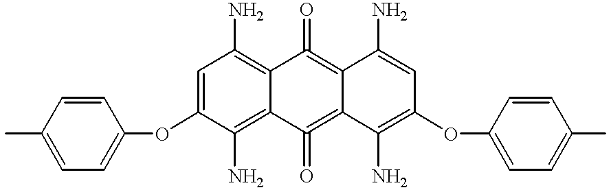
were added to the MLCP mixture. This mixture was dissolved to 30% in anisole, centrifugally applied to a PPN layer illuminated with linear polarized light and cross-linked. If a polarizer was held with its transmission direction parallel or perpendicular to the direction of polarization of the PPN illumination, the white light was transmitted in one case, but at right angles thereto the layer was colored depending on the absorption spectrum of the dye. The dichroic ratio was 8:1. If in place of this a black mixture of dichroic dye molecules is used, the hybrid layer serves as a wide-band polarizer. As a result of the local irradiation of the PPN layer with different directions of, linear polarizing layers can be produced with azimuthally varying directions of polarization. These can be used in LC displays, e.g. in conjunction with the structured retarders and orientating layers in the Examples hereinbefore.
Upon reading the present specification, various alternative embodiments will become obvious to those skilled in the art. These embodiments are to be considered within the scope and spirit of the invention which is only to be limited by the claims which follow and their equivalents.
Claims (18)
1. An optical component having a layer structure, which comprises only one substrate, a first orientating layer, a cross-linked liquid crystalline monomer layer, and a second orientating layer, the first orientating layer and the second orientating layer being located on opposite sides of the liquid crystalline monomer layer, with at least one of the orientating layers comprising a photo-oriented material.
2. The optical component according to claim 1 , wherein at least one of the orientating layers has a locally varying orientation pattern.
3. The optical component according to claim 1 further comprising an additional anisotropic layer of oriented cross-linked liquid crystal monomers located adjacent the second orientating layer.
4. The optical component according to claim 3 , wherein one of the cross-linked liquid crystal monomer layers is an optical retarder.
5. The optical component according to claim 4 further comprising a plurality of liquid crystal monomer layers functioning as optical retarders.
6. The optical component according to claim 4 wherein one of the cross-linked liquid crystalline monomer layer is constructed as a twisted optical retarder, and incorporates a cholesteric liquid crystal material.
7. The optical component according to claim 3 , wherein one or more of the liquid crystalline monomers layers comprises a highly twisted cholesteric liquid crystal material so as to act as an optical filter or circular polarizer in predetermined light wavelength ranges.
8. The optical component according to claim 1 , wherein the second orientating layer has a surface orientation structure produced by rubbing or oblique sputtering.
9. The optical component according to claim 1 , wherein an isotropic de-coupling layer is provided between the liquid crystalline monomer layer and the second orientation layer.
10. The optical component of claim 1 , wherein one or more of the first orientating layer, the second orientating layer, and the cross-linked liquid crystal monomer layer cover only a portion of the substrate.
11. The optical component according to claim 1 , wherein the liquid crystalline monomer layer comprises a highly twisted cholesteric liquid crystal material so as to act as an optical filter or circular polarizer in certain light wavelength ranges.
12. The optical component according to claim 1 further comprising an absorptive color filter layer.
13. The optical component of claim 1 , wherein the liquid crystalline monomer layer is ferroelectric.
14. The optical component according to claim 1 , wherein the liquid crystalline monomer layer has non-linear optical activity.
15. The optical component according to claim 1 further comprising a second cross-linked liquid crystal monomer layer and a second photo-oriented material, which is a photo-orientating polymer network layer, wherein the uppermost monomer layer is constructed as an orientating layer.
16. The optical component according to claim 1 , wherein the liquid crystalline monomer layer contains dichroic dye molecules.
17.The optical component according to claim 1 , wherein the liquid crystalline monomer layer consists essentially of a cross-linked monomer or a monomer mixture which in the monomeric state is liquid crystalline between a temperature range of about 15° C. and about 80° C., at least while being processed.
18. The optical component according to claim 17 , wherein the temperature range is from about 15° C. to about 50° C.
19. The optical component according to claim 1 , wherein the photo-oriented material is a photo-oriented polymer network.
Priority Applications (2)
| Application Number | Priority Date | Filing Date | Title |
|---|---|---|---|
| US09/779,611 US6369869B2 (en) | 1993-02-17 | 2001-02-09 | Optical component and method of manufacture |
| US10/076,565 US6717644B2 (en) | 1993-02-17 | 2002-02-19 | Optical component and method of manufacture |
Applications Claiming Priority (9)
| Application Number | Priority Date | Filing Date | Title |
|---|---|---|---|
| CH488/93 | 1993-02-17 | ||
| CH48893 | 1993-02-17 | ||
| US08/194,234 US5602661A (en) | 1993-02-17 | 1994-02-10 | Optical component |
| CH201694 | 1994-06-24 | ||
| CH2016/94 | 1994-06-24 | ||
| US48986595A | 1995-06-13 | 1995-06-13 | |
| US08/721,509 US6160597A (en) | 1993-02-17 | 1996-09-26 | Optical component and method of manufacture |
| US55011100A | 2000-04-14 | 2000-04-14 | |
| US09/779,611 US6369869B2 (en) | 1993-02-17 | 2001-02-09 | Optical component and method of manufacture |
Related Parent Applications (1)
| Application Number | Title | Priority Date | Filing Date |
|---|---|---|---|
| US55011100A Continuation | 1993-02-17 | 2000-04-14 |
Related Child Applications (1)
| Application Number | Title | Priority Date | Filing Date |
|---|---|---|---|
| US10/076,565 Continuation US6717644B2 (en) | 1993-02-17 | 2002-02-19 | Optical component and method of manufacture |
Publications (2)
| Publication Number | Publication Date |
|---|---|
| US20010030727A1 US20010030727A1 (en) | 2001-10-18 |
| US6369869B2 true US6369869B2 (en) | 2002-04-09 |
Family
ID=27172145
Family Applications (3)
| Application Number | Title | Priority Date | Filing Date |
|---|---|---|---|
| US08/721,509 Expired - Lifetime US6160597A (en) | 1993-02-17 | 1996-09-26 | Optical component and method of manufacture |
| US09/779,611 Expired - Lifetime US6369869B2 (en) | 1993-02-17 | 2001-02-09 | Optical component and method of manufacture |
| US10/076,565 Expired - Fee Related US6717644B2 (en) | 1993-02-17 | 2002-02-19 | Optical component and method of manufacture |
Family Applications Before (1)
| Application Number | Title | Priority Date | Filing Date |
|---|---|---|---|
| US08/721,509 Expired - Lifetime US6160597A (en) | 1993-02-17 | 1996-09-26 | Optical component and method of manufacture |
Family Applications After (1)
| Application Number | Title | Priority Date | Filing Date |
|---|---|---|---|
| US10/076,565 Expired - Fee Related US6717644B2 (en) | 1993-02-17 | 2002-02-19 | Optical component and method of manufacture |
Country Status (1)
| Country | Link |
|---|---|
| US (3) | US6160597A (en) |
Cited By (32)
| Publication number | Priority date | Publication date | Assignee | Title |
|---|---|---|---|---|
| US20030178609A1 (en) * | 2002-02-06 | 2003-09-25 | Merck Patent Gmbh | Birefringent film and its use |
| US6646703B1 (en) * | 1999-02-03 | 2003-11-11 | Rolic Ag | Method of making an element of liquid crystal polymer using alignment induced by unpolarized or circularly polarized radiation |
| US6693689B1 (en) * | 1999-03-31 | 2004-02-17 | Lg Philips Lcd Co., Ltd. | Reflective liquid crystal display device |
| US6717644B2 (en) | 1993-02-17 | 2004-04-06 | Rolic Ag | Optical component and method of manufacture |
| US6734936B1 (en) * | 1997-05-09 | 2004-05-11 | Rolic, Ag | Optical element containing an optically anisotropic layer having at least two regions with different molecular orientations |
| US20050004361A1 (en) * | 2003-07-01 | 2005-01-06 | Anil Kumar | Photochromic compounds |
| US20050003107A1 (en) * | 2003-07-01 | 2005-01-06 | Anil Kumar | Alignment facilities for optical dyes |
| US20050012998A1 (en) * | 2003-07-01 | 2005-01-20 | Anil Kumar | Polarizing, photochromic devices and methods of making the same |
| US6847457B2 (en) | 2002-10-29 | 2005-01-25 | Mitutoyo Corporation | Interferometer using integrated imaging array and high-density phase-shifting array |
| US20050083464A1 (en) * | 2002-04-16 | 2005-04-21 | 3M Innovative Properties Company And Rolic Ag | Compensators for liquid crystal displays and the use and manufacture of the compensators |
| US20050151926A1 (en) * | 2004-01-14 | 2005-07-14 | Anil Kumar | Polarizing devices and methods of making the same |
| US20050195479A1 (en) * | 2003-11-28 | 2005-09-08 | Dai Nippon Printing Co., Ltd. | Optical element, process for producing the same, substrate for liquid crystal alignment, liquid crystal display device, and birefringent material |
| US20060197068A1 (en) * | 1998-06-11 | 2006-09-07 | Rolic Ag | Optical component, orientation layer, and layerable polymerisable mixture |
| US20070041073A1 (en) * | 2004-05-17 | 2007-02-22 | Anil Kumar | Polarizing, photochromic devices and methods of making the same |
| US20080129928A1 (en) * | 2006-12-01 | 2008-06-05 | Taiwan Tft Lcd Association | Optical film and manufacturing method thereof and substrate structure and display panel using the optical film |
| US20080246894A1 (en) * | 2004-01-12 | 2008-10-09 | Securency Pty Limited | Security Document Incorporating Optical Component |
| US20080274304A1 (en) * | 2005-09-20 | 2008-11-06 | Mohammed Zoubair Cherkaoui | Functionalized Photoreactive Compounds |
| US20100073604A1 (en) * | 2008-09-22 | 2010-03-25 | Sony Corporation | Retardation film, method of manufacturing the same, and display |
| US20100266821A1 (en) * | 2007-12-21 | 2010-10-21 | Rolic Ag | Functionalized photoreactive compounds |
| US20100266814A1 (en) * | 2007-12-21 | 2010-10-21 | Rolic Ag | Photoalignment composition |
| US20110080628A1 (en) * | 2003-07-01 | 2011-04-07 | Transitions Optical, Inc. | Clear to circular polarizing photochromic devices |
| US8211338B2 (en) | 2003-07-01 | 2012-07-03 | Transitions Optical, Inc | Photochromic compounds |
| US8518546B2 (en) | 2003-07-01 | 2013-08-27 | Transitions Optical, Inc. | Photochromic compounds and compositions |
| US8545015B2 (en) | 2003-07-01 | 2013-10-01 | Transitions Optical, Inc. | Polarizing photochromic articles |
| US8545984B2 (en) | 2003-07-01 | 2013-10-01 | Transitions Optical, Inc. | Photochromic compounds and compositions |
| US8582192B2 (en) | 2003-07-01 | 2013-11-12 | Transitions Optical, Inc. | Polarizing photochromic articles |
| US8698117B2 (en) | 2003-07-01 | 2014-04-15 | Transitions Optical, Inc. | Indeno-fused ring compounds |
| US9096014B2 (en) | 2003-07-01 | 2015-08-04 | Transitions Optical, Inc. | Oriented polymeric sheets exhibiting dichroism and articles containing the same |
| WO2018158254A2 (en) | 2017-03-03 | 2018-09-07 | Rolic Technologies AG | New photoalignment composition for the stabilization of the pre-tilt angle in liquid crystal layers |
| US10866455B2 (en) | 2017-10-19 | 2020-12-15 | Ppg Industries Ohio, Inc. | Display devices including photochromic-dichroic compounds and dichroic compounds |
| US11439433B2 (en) * | 2016-06-10 | 2022-09-13 | University of Pittsburgh—of the Commonwealth System of Higher Education | Optically transparent polymeric actuator and display apparatus employing same |
| US11739268B2 (en) | 2016-06-10 | 2023-08-29 | University Of Pittsburgh-Of The Commonwealth System Of Higher Education | Optically transparent polymeric actuator and display apparatus employing same |
Families Citing this family (134)
| Publication number | Priority date | Publication date | Assignee | Title |
|---|---|---|---|---|
| KR100208970B1 (en) | 1995-12-29 | 1999-07-15 | 구자홍 | A lc cell and a fabrication method thereof |
| US6496287B1 (en) * | 1998-04-09 | 2002-12-17 | Rolic Ag | Optical identification element |
| US6376467B1 (en) * | 1998-10-09 | 2002-04-23 | The Regents Of The University Of California | Use of inhibitors of protein kinase C epsilon to treat pain |
| US6897073B2 (en) * | 1998-07-14 | 2005-05-24 | Zyomyx, Inc. | Non-specific binding resistant protein arrays and methods for making the same |
| US20040120040A1 (en) * | 1998-11-13 | 2004-06-24 | Rolic Ag | Optical component |
| US6643001B1 (en) * | 1998-11-20 | 2003-11-04 | Revco, Inc. | Patterned platelets |
| JP2000162581A (en) * | 1998-12-01 | 2000-06-16 | Sharp Corp | Reflection type liquid crystal display device and its production |
| AUPQ125999A0 (en) | 1999-06-28 | 1999-07-22 | Securency Pty Ltd | Method of producing a diffractive structure in security documents |
| US6939587B1 (en) * | 1999-09-03 | 2005-09-06 | Kent State University | Fabrication of aligned crystal cell/film by simultaneous alignment and phase separation |
| EP1120737A1 (en) * | 2000-01-27 | 2001-08-01 | Rolic AG | Optical security device |
| US6783814B2 (en) | 2000-08-21 | 2004-08-31 | Massachusetts Institute Of Technology | Polymers with high internal free volume |
| WO2002050581A1 (en) * | 2000-12-20 | 2002-06-27 | Dai Nippon Printing Co., Ltd. | Circularly polarized light extraction optical element and method of manufacturing the optical element |
| EP1219651A1 (en) * | 2000-12-29 | 2002-07-03 | Rolic AG | Photoactive copolymer |
| US6490076B2 (en) * | 2001-01-11 | 2002-12-03 | Hrl Laboratories, Llc | Optical phased array for depolarized optical beam control |
| EP1227347A1 (en) * | 2001-01-29 | 2002-07-31 | Rolic AG | Optical device and method for manufacturing same |
| US20030090012A1 (en) * | 2001-09-27 | 2003-05-15 | Allen Richard Charles | Methods of making polarization rotators and articles containing the polarization rotators |
| US6985291B2 (en) * | 2001-10-01 | 2006-01-10 | 3M Innovative Properties Company | Non-inverting transflective assembly |
| US7193670B2 (en) * | 2002-04-17 | 2007-03-20 | Nitto Denko Corporation | Compensator for liquid crystal display with two compensation sheets |
| AUPS301902A0 (en) * | 2002-06-18 | 2002-07-11 | Securency Pty Ltd | Polarising liquid crystal device for security documents |
| US20040008306A1 (en) * | 2002-07-12 | 2004-01-15 | Eastman Kodak Company | Optical compensator with surfactant addenda and process |
| US6582775B1 (en) * | 2002-07-12 | 2003-06-24 | Eastman Kodak Company | Process for making an optical compensator film comprising photo-aligned orientation layer |
| US6894751B2 (en) * | 2002-07-12 | 2005-05-17 | Eastman Kodak Company | Process for making an optical compensator film comprising an anisotropic nematic liquid crystal |
| US6874899B2 (en) * | 2002-07-12 | 2005-04-05 | Eastman Kodak Company | Apparatus and method for irradiating a substrate |
| US20040008307A1 (en) * | 2002-07-12 | 2004-01-15 | Eastman Kodak Company | Optical compensator with solvent and process |
| US20040008303A1 (en) * | 2002-07-12 | 2004-01-15 | Eastman Kodak Company | Nematic liquid crystal compensator with barrier layer and process |
| US6943930B2 (en) * | 2002-09-12 | 2005-09-13 | Eastman Kodak Company | Method and system for fabricating optical film using an exposure source and reflecting surface |
| EP1462485A1 (en) * | 2003-03-26 | 2004-09-29 | Rolic AG | Polymerizable dichroic azo dyes |
| WO2004090627A1 (en) * | 2003-04-08 | 2004-10-21 | Merck Patent Gmbh | Compensated lcd of the ips mode |
| US6844913B2 (en) * | 2003-04-24 | 2005-01-18 | Eastman Kodak Company | Optical exposure apparatus for forming an alignment layer |
| US20040263974A1 (en) * | 2003-06-26 | 2004-12-30 | Optical Coating Laboratory Inc., A Jds Unipahse Company And A Corporation Of The State Of Delware | Flat polarization conversion system with patterned retarder |
| WO2005081779A2 (en) * | 2004-02-19 | 2005-09-09 | Kent Displays Incorporated | Staked display with shared electrode addressing |
| US7075606B2 (en) * | 2003-07-29 | 2006-07-11 | Eastman Kodak Company | Method for manufacturing an optical compensator on a transitional substrate |
| JP2005049493A (en) * | 2003-07-31 | 2005-02-24 | Dainippon Printing Co Ltd | Film with alignment layer for optical element |
| US7626661B2 (en) * | 2003-12-11 | 2009-12-01 | Jds Uniphase Corporation | Polarization controlling elements |
| US7097888B2 (en) * | 2003-12-15 | 2006-08-29 | Eastman Kodak Company | Aligned liquid crystal layer containing azolium salts and process for increasing the tilt |
| US20050129875A1 (en) * | 2003-12-15 | 2005-06-16 | Eastman Kodak Company | Aligned liquid crystal layer containing onium salts and process for increasing the tilt |
| JP4530256B2 (en) * | 2004-01-19 | 2010-08-25 | 日東電工株式会社 | Retardation film, method for producing the same, and optical film using the same |
| US7553521B2 (en) * | 2004-01-22 | 2009-06-30 | Dai Nippon Printing Co., Ltd. | Liquid crystal displays |
| JP4537718B2 (en) * | 2004-01-22 | 2010-09-08 | 大日本印刷株式会社 | Liquid crystal display element |
| US7553525B2 (en) * | 2004-01-22 | 2009-06-30 | Dai Nippon Printing Co., Ltd. | Liquid crystal display |
| US20080166528A1 (en) * | 2004-02-05 | 2008-07-10 | Securency Pty Limited | Method and Apparatus for Manufacturing an Optical Component |
| US7088510B2 (en) * | 2004-02-23 | 2006-08-08 | Jds Uniphase Corporation | Anti-aliasing optical filter for image sensors |
| US7087965B2 (en) * | 2004-04-22 | 2006-08-08 | International Business Machines Corporation | Strained silicon CMOS on hybrid crystal orientations |
| JP4797468B2 (en) | 2004-07-07 | 2011-10-19 | 大日本印刷株式会社 | Phase difference control member, manufacturing method thereof, and liquid crystal display device |
| US7527836B2 (en) * | 2004-12-28 | 2009-05-05 | Dai Nippon Printing Co., Ltd. | Optical element and method for manufacturing the same |
| KR101212135B1 (en) * | 2005-06-14 | 2012-12-14 | 엘지디스플레이 주식회사 | Liquid Crystal Display Device, and method of fabricating the same |
| JP5154418B2 (en) | 2005-08-19 | 2013-02-27 | リアルディー インコーポレイテッド | Stereoscopic eyewear |
| TWI406061B (en) * | 2005-11-10 | 2013-08-21 | Dainippon Ink & Chemicals | Composition for photoalignment film, optically anisotropic body and method of producing same |
| TWI331688B (en) * | 2005-11-11 | 2010-10-11 | Ind Tech Res Inst | Reflective liquid crystal display assembly |
| US20070141244A1 (en) * | 2005-12-19 | 2007-06-21 | Eastman Kodak Company | Method of making a polarizer plate |
| US7732007B2 (en) * | 2005-12-19 | 2010-06-08 | Eastman Kodak Company | Method of making a polarizer plate |
| DE102006023084B4 (en) * | 2006-05-16 | 2019-07-18 | Leonhard Kurz Stiftung & Co. Kg | Value document with security element |
| WO2007137334A1 (en) * | 2006-05-31 | 2007-12-06 | Securency International Pty Ltd | Security document incorporating optical component |
| EP1892706B1 (en) * | 2006-08-23 | 2012-06-13 | JDS Uniphase Corporation | Optical pick-up unit |
| JP4740091B2 (en) * | 2006-11-07 | 2011-08-03 | Jx日鉱日石エネルギー株式会社 | Latent image forming film, latent image identification kit, and latent image identification method |
| JP4978995B2 (en) * | 2006-11-08 | 2012-07-18 | 株式会社ジャパンディスプレイイースト | Liquid crystal display |
| WO2008092038A1 (en) | 2007-01-24 | 2008-07-31 | Ravenbrick, Llc | Thermally switched optical downconverting filter |
| US7906214B2 (en) * | 2007-01-26 | 2011-03-15 | Transitions Optical, Inc. | Optical elements comprising compatiblizing coatings and methods of making the same |
| DE102007022264A1 (en) * | 2007-05-09 | 2008-11-13 | Leonhard Kurz Gmbh & Co. Kg | Foil element with polymer layer |
| EP2171520A4 (en) | 2007-07-11 | 2011-09-07 | Ravenbrick Llc | Thermally switched reflective optical shutter |
| KR101303981B1 (en) | 2007-09-19 | 2013-09-04 | 라벤브릭 엘엘씨 | Low-emissivity window films and coatings incorporating nanoscale wire grids |
| DE102008056221A1 (en) | 2007-11-30 | 2009-06-04 | Merck Patent Gmbh | Polymerizable compounds |
| US8169685B2 (en) | 2007-12-20 | 2012-05-01 | Ravenbrick, Llc | Thermally switched absorptive window shutter |
| CA2754619C (en) | 2008-04-23 | 2014-04-01 | Ravenbrick, Llc | Glare management of reflective and thermoreflective surfaces |
| US9116302B2 (en) | 2008-06-19 | 2015-08-25 | Ravenbrick Llc | Optical metapolarizer device |
| CA2737041C (en) | 2008-08-20 | 2013-10-15 | Ravenbrick, Llc | Methods for fabricating thermochromic filters |
| US8531627B2 (en) * | 2008-12-25 | 2013-09-10 | Dai Nippon Printing Co., Ltd. | Optical rotation plate and liquid crystal display device using the same |
| EP2218764B1 (en) | 2009-02-13 | 2012-01-18 | Merck Patent GmbH | Chiral reactive mesogen mixture |
| US8284336B2 (en) | 2009-04-10 | 2012-10-09 | Ravenbrick Llc | Thermally switched optical filter incorporating a guest-host architecture |
| US8947760B2 (en) | 2009-04-23 | 2015-02-03 | Ravenbrick Llc | Thermotropic optical shutter incorporating coatable polarizers |
| EP2494004B1 (en) | 2009-10-30 | 2013-09-25 | Merck Patent GmbH | Polymerisable lc material and polymer film with negative optical dispersion |
| US8867132B2 (en) * | 2009-10-30 | 2014-10-21 | Ravenbrick Llc | Thermochromic filters and stopband filters for use with same |
| WO2011062708A2 (en) | 2009-11-17 | 2011-05-26 | Ravenbrick Llc | Thermally switched optical filter incorporating a refractive optical structure |
| KR101476899B1 (en) * | 2010-03-29 | 2014-12-26 | 라벤브릭 엘엘씨 | Polymer-stabilized thermotropic liquid crystal device |
| CA2801399C (en) | 2010-06-01 | 2016-03-29 | Ravenbrick, Llc | Multifunctional building component |
| US10254453B2 (en) * | 2010-11-02 | 2019-04-09 | Arizona Board Of Regents On Behalf Of The University Of Arizona | Thin-film broadband and wide-angle devices for generating and sampling polarization states |
| WO2015002708A2 (en) * | 2013-05-28 | 2015-01-08 | The Arizona Board Of Regents On Behalf Of The University Of Arizona | Thin-film broadband and wide-angle devices for generating and sampling polarization states |
| TWI437332B (en) | 2011-10-27 | 2014-05-11 | Far Eastern New Century Corp | A method for preparing composite phase difference plate |
| KR102093832B1 (en) | 2012-02-08 | 2020-03-26 | 메르크 파텐트 게엠베하 | Reactive mesogen formulation with conductive additive |
| US9671538B2 (en) * | 2012-11-19 | 2017-06-06 | The Arizona Board Of Regents On Behalf Of The University Of Arizona | Optical elements comprising cholesteric liquid crystal polymers |
| US9644145B2 (en) | 2012-12-14 | 2017-05-09 | Merck Patent Gmbh | Birefringent RM lens |
| CN104870609A (en) | 2012-12-21 | 2015-08-26 | 默克专利股份有限公司 | Reactive mesogens |
| US10286616B2 (en) * | 2013-08-19 | 2019-05-14 | Rolic Ag | Photo-alignable object |
| WO2015124483A1 (en) | 2014-02-19 | 2015-08-27 | Rolic Ag | Liquid crystal alignment composition, liquid crystal alignment film and liquid crystal display element |
| JP2017518413A (en) | 2014-05-21 | 2017-07-06 | ロリク アーゲーRolic Ag | Polymerizable dichroic dye |
| WO2016016156A1 (en) | 2014-07-31 | 2016-02-04 | Rolic Ag | Encapsulation structure for an oled display incorporating antireflection properties |
| EP3308201A1 (en) | 2015-06-15 | 2018-04-18 | 3M Innovative Properties Company | Optical stack including reflecting-absorbing polarizer |
| JP6494751B2 (en) | 2015-09-03 | 2019-04-03 | スリーエム イノベイティブ プロパティズ カンパニー | Head mounted display |
| CN108349177B (en) * | 2015-10-30 | 2021-02-09 | 光学转变公司 | Method of making an optical article having gradient light influencing properties |
| WO2017074434A1 (en) * | 2015-10-30 | 2017-05-04 | Transitions Optical, Inc. | Optical articles and method of preparing the same |
| KR102480724B1 (en) | 2015-10-30 | 2022-12-22 | 트랜지션즈 옵티칼 인코포레이티드 | Optical product having gradient light response and method for manufacturing the same |
| EP3368926B1 (en) * | 2015-10-30 | 2024-03-06 | Transitions Optical Ltd. | A method of making an optical article with an inkjet printing device |
| JP7284581B2 (en) | 2016-05-17 | 2023-05-31 | メルク パテント ゲゼルシャフト ミット ベシュレンクテル ハフツング | Polymerizable liquid crystal materials and polymerized liquid crystal films |
| EP3246378B1 (en) | 2016-05-17 | 2019-03-20 | Merck Patent GmbH | Polymerisable liquid crystal material and polymerised liquid crystal film |
| CN109477930A (en) | 2016-07-29 | 2019-03-15 | 罗利克技术有限公司 | The method of orientation is generated on liquid crystal polymer material |
| WO2018060110A1 (en) | 2016-09-28 | 2018-04-05 | Merck Patent Gmbh | Polymerisable liquid crystal material and polymerised liquid crystal film |
| JP7101182B2 (en) | 2016-11-15 | 2022-07-14 | スリーエム イノベイティブ プロパティズ カンパニー | Optical lenses and eyewear including optical lenses |
| US20200071618A1 (en) | 2016-12-01 | 2020-03-05 | Merck Patent Gmbh | Polymerisable liquid crystal material and polymerised liquid crystal film |
| CN110088672A (en) | 2016-12-20 | 2019-08-02 | 3M创新有限公司 | Optical system |
| US11156757B2 (en) | 2017-03-06 | 2021-10-26 | 3M Innovative Properties Company | High contrast optical film and devices including the same |
| WO2018163009A1 (en) | 2017-03-06 | 2018-09-13 | 3M Innovative Properties Company | High contrast optical film and devices including the same |
| WO2018178817A2 (en) | 2017-03-31 | 2018-10-04 | 3M Innovative Properties Company | Optical system |
| KR20200041922A (en) | 2017-08-15 | 2020-04-22 | 메르크 파텐트 게엠베하 | Polymerizable liquid crystal material and polymerized liquid crystal film |
| CN111344613B (en) | 2017-10-09 | 2022-09-27 | 3M创新有限公司 | Optical component and optical system |
| CN111316146B (en) | 2017-10-10 | 2022-06-03 | 3M创新有限公司 | Curved reflective polarizing film and method of forming the same |
| CN114296173A (en) | 2017-10-25 | 2022-04-08 | 3M创新有限公司 | Optical system |
| KR20200074181A (en) | 2017-10-27 | 2020-06-24 | 쓰리엠 이노베이티브 프로퍼티즈 컴파니 | Optical system |
| JP7257394B2 (en) | 2017-10-27 | 2023-04-13 | スリーエム イノベイティブ プロパティズ カンパニー | Patterned optical retarder and manufacturing method thereof |
| CN112041414A (en) | 2018-04-27 | 2020-12-04 | 默克专利股份有限公司 | Polymerizable liquid crystal material and polymerized liquid crystal film |
| WO2019206925A1 (en) | 2018-04-27 | 2019-10-31 | Merck Patent Gmbh | Polymerisable liquid crystal material and polymerised liquid crystal film |
| CN112400125B (en) | 2018-07-13 | 2024-03-12 | 3M创新有限公司 | Optical system and optical film |
| CN112739801A (en) | 2018-08-13 | 2021-04-30 | 默克专利股份有限公司 | Polymerizable liquid crystal material and polymerized liquid crystal film |
| CN112534023A (en) | 2018-08-13 | 2021-03-19 | 默克专利股份有限公司 | Polymerizable liquid crystal material and polymerized liquid crystal film |
| US20210294012A1 (en) | 2018-08-14 | 2021-09-23 | 3M Innovative Properties Company | Optical system |
| JP2022510013A (en) | 2018-12-03 | 2022-01-25 | メルク・パテント・ゲゼルシヤフト・ミツト・ベシユレンクテル・ハフツング | Polymerizable liquid crystal materials and polymerized liquid crystal films |
| KR20210102363A (en) | 2018-12-12 | 2021-08-19 | 메르크 파텐트 게엠베하 | Polymerizable Liquid Crystal Ink Formulations |
| KR20210142672A (en) | 2019-03-18 | 2021-11-25 | 메르크 파텐트 게엠베하 | Polymeric liquid crystal material and polymerized liquid crystal film |
| CN113785032A (en) | 2019-04-30 | 2021-12-10 | 默克专利股份有限公司 | Reactive mesogen |
| WO2021013780A1 (en) | 2019-07-24 | 2021-01-28 | Rolic Technologies AG | Photo-alignable positive c-plate retarder |
| CN114556194A (en) * | 2019-09-27 | 2022-05-27 | 3M创新有限公司 | Color neutral emitting display with notched reflective polarizer |
| KR20220123003A (en) | 2019-12-26 | 2022-09-05 | 쓰리엠 이노베이티브 프로퍼티즈 컴파니 | Film stacks for thin circular polarizers |
| TW202200630A (en) | 2020-04-30 | 2022-01-01 | 德商馬克專利公司 | Polymerizable liquid crystal material and polymerized liquid crystal film |
| WO2021259825A1 (en) | 2020-06-23 | 2021-12-30 | Merck Patent Gmbh | Polymerisable liquid crystal material and polymerised liquid crystal film |
| WO2022063902A1 (en) | 2020-09-24 | 2022-03-31 | Merck Patent Gmbh | Polymerizable liquid crystal material and polymerized liquid crystal film |
| EP4039776A3 (en) | 2020-11-20 | 2022-08-24 | Merck Patent GmbH | Polymerisable lc material and polymer film |
| EP4008759A1 (en) | 2020-11-20 | 2022-06-08 | Merck Patent GmbH | Polymerisable liquid crystal material and polymerised liquid crystal film |
| GB2603274A (en) | 2020-12-04 | 2022-08-03 | Merck Patent Gmbh | Polymerizable liquid crystal material and polymerized liquid crystal film |
| CN117280011A (en) | 2021-05-07 | 2023-12-22 | 默克专利股份有限公司 | Reactive mesogen |
| WO2023237572A1 (en) | 2022-06-10 | 2023-12-14 | Merck Patent Gmbh | Polymerisable liquid crystal medium and polymerised liquid crystal film |
| US11745420B1 (en) | 2022-06-23 | 2023-09-05 | Lawrence Livermore National Security, Llc | Stereolithography additive manufacturing of magnetically aligned liquid crystal elastomers |
| US11794406B1 (en) * | 2022-06-23 | 2023-10-24 | Lawrence Livermore National Security, Llc | Stereolithography additive manufacturing of photoaligned liquid crystal elastomers |
| WO2024042008A1 (en) | 2022-08-23 | 2024-02-29 | Merck Patent Gmbh | Polymerizable liquid crystal material and polymerized liquid crystal film |
| WO2024052363A1 (en) | 2022-09-08 | 2024-03-14 | Merck Patent Gmbh | Polymerizable liquid crystal material and polymerized liquid crystal film |
| WO2024061796A1 (en) | 2022-09-21 | 2024-03-28 | Merck Patent Gmbh | Polymerisable liquid crystal medium and polymerised liquid crystal film |
Citations (19)
| Publication number | Priority date | Publication date | Assignee | Title |
|---|---|---|---|---|
| US4615962A (en) | 1979-06-25 | 1986-10-07 | University Patents, Inc. | Diacetylenes having liquid crystal phases |
| US4617371A (en) | 1982-11-29 | 1986-10-14 | Alexandre Blumstein | Novel polymeric liquid crystals and methods for their preparation |
| US4637896A (en) | 1982-12-15 | 1987-01-20 | Armstrong World Industries, Inc. | Polymeric liquid crystals |
| US4696990A (en) | 1986-03-31 | 1987-09-29 | Eastman Kodak Company | Novel photocrosslinkable liquid crystalline polymers |
| EP0331233A2 (en) | 1988-02-29 | 1989-09-06 | Koninklijke Philips Electronics N.V. | Method of manufacturing a laminated element and the element thus obtained |
| EP0336321A2 (en) | 1988-04-04 | 1989-10-11 | Idemitsu Kosan Company Limited | Process for producing liquid crystal optical device |
| EP0397263A1 (en) | 1989-05-10 | 1990-11-14 | Koninklijke Philips Electronics N.V. | Method of manufacturing a polarisation filter, a polarisation filter thus obtained and a display having such a polarisation filter |
| US4974941A (en) | 1989-03-08 | 1990-12-04 | Hercules Incorporated | Process of aligning and realigning liquid crystal media |
| US5073294A (en) | 1990-03-07 | 1991-12-17 | Hercules Incorporated | Process of preparing compositions having multiple oriented mesogens |
| US5138010A (en) | 1990-06-25 | 1992-08-11 | University Of Colorado Foundation, Inc. | Fast switching polysiloxane ferroelectric liquid crystals |
| EP0525473A2 (en) | 1991-07-26 | 1993-02-03 | F. Hoffmann-La Roche Ag | Display device with liquid crystal cell |
| EP0525478A2 (en) | 1991-07-26 | 1993-02-03 | F. Hoffmann-La Roche Ag | Liquid crystal display cell |
| US5202053A (en) | 1991-02-22 | 1993-04-13 | Hercules Incorporated | Polymerizable nematic monomer compositions |
| EP0543678A1 (en) | 1991-11-22 | 1993-05-26 | Nippon Oil Company, Limited | Process for producing heat-resistant optical elements |
| EP0569809A1 (en) | 1992-05-13 | 1993-11-18 | F. Hoffmann-La Roche Ag | Process and means for disinclination-free planar orientation of chiral liquid cristalline side chain polymers |
| US5325218A (en) | 1992-12-31 | 1994-06-28 | Minnesota Mining And Manufacturing Company | Cholesteric polarizer for liquid crystal display and overhead projector |
| EP0611981A1 (en) | 1993-02-17 | 1994-08-24 | F. Hoffmann-La Roche Ag | Optical device |
| US5389698A (en) | 1991-07-26 | 1995-02-14 | Hoffmann-La Roche Inc. | Process for making photopolymers having varying molecular orientation using light to orient and polymerize |
| US5464669A (en) | 1993-09-18 | 1995-11-07 | Goldstar Co., Ltd. | Method for forming an orientation film of photopolymer in a liquid crystal display |
Family Cites Families (1)
| Publication number | Priority date | Publication date | Assignee | Title |
|---|---|---|---|---|
| US6160597A (en) | 1993-02-17 | 2000-12-12 | Rolic Ag | Optical component and method of manufacture |
-
1996
- 1996-09-26 US US08/721,509 patent/US6160597A/en not_active Expired - Lifetime
-
2001
- 2001-02-09 US US09/779,611 patent/US6369869B2/en not_active Expired - Lifetime
-
2002
- 2002-02-19 US US10/076,565 patent/US6717644B2/en not_active Expired - Fee Related
Patent Citations (20)
| Publication number | Priority date | Publication date | Assignee | Title |
|---|---|---|---|---|
| US4615962A (en) | 1979-06-25 | 1986-10-07 | University Patents, Inc. | Diacetylenes having liquid crystal phases |
| US4617371A (en) | 1982-11-29 | 1986-10-14 | Alexandre Blumstein | Novel polymeric liquid crystals and methods for their preparation |
| US4637896A (en) | 1982-12-15 | 1987-01-20 | Armstrong World Industries, Inc. | Polymeric liquid crystals |
| US4696990A (en) | 1986-03-31 | 1987-09-29 | Eastman Kodak Company | Novel photocrosslinkable liquid crystalline polymers |
| EP0331233A2 (en) | 1988-02-29 | 1989-09-06 | Koninklijke Philips Electronics N.V. | Method of manufacturing a laminated element and the element thus obtained |
| EP0336321A2 (en) | 1988-04-04 | 1989-10-11 | Idemitsu Kosan Company Limited | Process for producing liquid crystal optical device |
| US4974941A (en) | 1989-03-08 | 1990-12-04 | Hercules Incorporated | Process of aligning and realigning liquid crystal media |
| EP0397263A1 (en) | 1989-05-10 | 1990-11-14 | Koninklijke Philips Electronics N.V. | Method of manufacturing a polarisation filter, a polarisation filter thus obtained and a display having such a polarisation filter |
| US5024850A (en) | 1989-05-10 | 1991-06-18 | U.S. Philips Corporation | Method of manufacturing a polarization filter and a polarization filter so obtained |
| US5073294A (en) | 1990-03-07 | 1991-12-17 | Hercules Incorporated | Process of preparing compositions having multiple oriented mesogens |
| US5138010A (en) | 1990-06-25 | 1992-08-11 | University Of Colorado Foundation, Inc. | Fast switching polysiloxane ferroelectric liquid crystals |
| US5202053A (en) | 1991-02-22 | 1993-04-13 | Hercules Incorporated | Polymerizable nematic monomer compositions |
| EP0525473A2 (en) | 1991-07-26 | 1993-02-03 | F. Hoffmann-La Roche Ag | Display device with liquid crystal cell |
| EP0525478A2 (en) | 1991-07-26 | 1993-02-03 | F. Hoffmann-La Roche Ag | Liquid crystal display cell |
| US5389698A (en) | 1991-07-26 | 1995-02-14 | Hoffmann-La Roche Inc. | Process for making photopolymers having varying molecular orientation using light to orient and polymerize |
| EP0543678A1 (en) | 1991-11-22 | 1993-05-26 | Nippon Oil Company, Limited | Process for producing heat-resistant optical elements |
| EP0569809A1 (en) | 1992-05-13 | 1993-11-18 | F. Hoffmann-La Roche Ag | Process and means for disinclination-free planar orientation of chiral liquid cristalline side chain polymers |
| US5325218A (en) | 1992-12-31 | 1994-06-28 | Minnesota Mining And Manufacturing Company | Cholesteric polarizer for liquid crystal display and overhead projector |
| EP0611981A1 (en) | 1993-02-17 | 1994-08-24 | F. Hoffmann-La Roche Ag | Optical device |
| US5464669A (en) | 1993-09-18 | 1995-11-07 | Goldstar Co., Ltd. | Method for forming an orientation film of photopolymer in a liquid crystal display |
Non-Patent Citations (8)
| Title |
|---|
| Derwent Abstract No. AN-93-037877/05. |
| Derwent Abstract No. AN-93-073882/05. |
| Derwent Abstract No. AN-93-36107/46. |
| Derwent Abstract No. AN-94-265517/33. |
| Geibel, K. et al., Advanced Materials, 5(2):107-109 (1993). |
| Hikmet, R.A.M., J. Appl. Phys., 70(3):1265-1269 (1991). |
| Research Disclosure No. 337. Emsworth. GB, pgs. 410-411 (May 1992). |
| Shannon, P.J. et al., Nature, 368:532-533 (1994). |
Cited By (92)
| Publication number | Priority date | Publication date | Assignee | Title |
|---|---|---|---|---|
| US6717644B2 (en) | 1993-02-17 | 2004-04-06 | Rolic Ag | Optical component and method of manufacture |
| US7679701B2 (en) | 1997-05-09 | 2010-03-16 | Rolic Ltd C/O Rolic Technologies Ltd | Optical element |
| US20080098488A1 (en) * | 1997-05-09 | 2008-04-24 | Rolic Ltd C/O Rolic Technologies Ltd | Optical element |
| US20060232734A1 (en) * | 1997-05-09 | 2006-10-19 | Rolic Ag | Element for protection against forgery or copying containing a structured retarder and a polarizer layer |
| US6734936B1 (en) * | 1997-05-09 | 2004-05-11 | Rolic, Ag | Optical element containing an optically anisotropic layer having at least two regions with different molecular orientations |
| US9643445B2 (en) | 1997-05-09 | 2017-05-09 | Rolic Ag | Optical element |
| US8830425B2 (en) | 1997-05-09 | 2014-09-09 | Rolic Ag | Optical element |
| US8553196B2 (en) | 1997-05-09 | 2013-10-08 | Rolic Ag | Optical element |
| US7292292B2 (en) | 1997-05-09 | 2007-11-06 | Rolic Ltd C/O Rolic Technologies Ltd. | Element for protection against forgery or copying containing a structured retarder and a polarizer layer |
| US7364671B2 (en) | 1998-06-11 | 2008-04-29 | Rolic Ltd C/O Rolic Technologies Ltd | Optical component, orientation layer, and layerable polymerisable mixture |
| US20060197068A1 (en) * | 1998-06-11 | 2006-09-07 | Rolic Ag | Optical component, orientation layer, and layerable polymerisable mixture |
| US6646703B1 (en) * | 1999-02-03 | 2003-11-11 | Rolic Ag | Method of making an element of liquid crystal polymer using alignment induced by unpolarized or circularly polarized radiation |
| US6693689B1 (en) * | 1999-03-31 | 2004-02-17 | Lg Philips Lcd Co., Ltd. | Reflective liquid crystal display device |
| US6924861B2 (en) * | 2002-02-06 | 2005-08-02 | Merck Patent Gmbh | Birefringement film containing liquid crystal material having multi domains with splayed structure |
| US20030178609A1 (en) * | 2002-02-06 | 2003-09-25 | Merck Patent Gmbh | Birefringent film and its use |
| US20060221286A1 (en) * | 2002-04-16 | 2006-10-05 | 3M Innovative Properties Company | Compensators For Liquid Crystal Displays and the Use and Manufacture of the Compensators |
| US6919946B2 (en) | 2002-04-16 | 2005-07-19 | 3M Innovative Properties Company | Compensators for liquid crystal displays and the use and manufacture of the compensators |
| US7088411B2 (en) | 2002-04-16 | 2006-08-08 | 3M Innovative Properties Company | Liquid crystal displays including two o-plates and two c-plates, with helical arrangement of azimuthal orientations |
| US20050083464A1 (en) * | 2002-04-16 | 2005-04-21 | 3M Innovative Properties Company And Rolic Ag | Compensators for liquid crystal displays and the use and manufacture of the compensators |
| US6847457B2 (en) | 2002-10-29 | 2005-01-25 | Mitutoyo Corporation | Interferometer using integrated imaging array and high-density phase-shifting array |
| US7466469B2 (en) | 2003-07-01 | 2008-12-16 | Ppg Industries Ohio, Inc. | Polarizing, photochromic devices and methods of making the same |
| US20050003107A1 (en) * | 2003-07-01 | 2005-01-06 | Anil Kumar | Alignment facilities for optical dyes |
| US10619018B2 (en) | 2003-07-01 | 2020-04-14 | Transitions Optical, Inc. | Oriented polymeric sheets exhibiting dichroism and articles containing the same |
| US10532997B2 (en) | 2003-07-01 | 2020-01-14 | Transitions Optical, Inc. | Photochromic compounds |
| US20070041071A1 (en) * | 2003-07-01 | 2007-02-22 | Anil Kumar | Polarizing, photochromic devices and methods of making the same |
| US20070047054A1 (en) * | 2003-07-01 | 2007-03-01 | Anil Kumar | Polarizing, photochromic devices and methods of making the same |
| US20070047055A1 (en) * | 2003-07-01 | 2007-03-01 | Anil Kumar | Polarizing, photochromic devices and methods of making the same |
| US20070053047A1 (en) * | 2003-07-01 | 2007-03-08 | Anil Kumar | Polarizing, photochromic devices and methods of making the same |
| US20070053049A1 (en) * | 2003-07-01 | 2007-03-08 | Anil Kumar | Polarizing, photochromic devices and methods of making the same |
| US20070053050A1 (en) * | 2003-07-01 | 2007-03-08 | Anil Kumar | Polarizing, photochromic devices and methods of making the same |
| US20070053048A1 (en) * | 2003-07-01 | 2007-03-08 | Anil Kumar | Polirizing, photochromic devices and methods of making the same |
| US20070075388A1 (en) * | 2003-07-01 | 2007-04-05 | Anil Kumar | Polarizing, photochromic devices and methods of making the same |
| US7256921B2 (en) | 2003-07-01 | 2007-08-14 | Transitions Optical, Inc. | Polarizing, photochromic devices and methods of making the same |
| US7286275B2 (en) | 2003-07-01 | 2007-10-23 | Transitions Optical, Inc. | Polarizing, photochromic devices and methods of making the same |
| US10532998B2 (en) | 2003-07-01 | 2020-01-14 | Transitions Optical, Inc. | Photochromic compounds |
| US7342112B2 (en) | 2003-07-01 | 2008-03-11 | Ppg Industries Ohio, Inc. | Photochromic compounds |
| US7349137B2 (en) | 2003-07-01 | 2008-03-25 | Ppg Industries Ohio, Inc. | Polarizing, photochromic devices and methods of making the same |
| US7349138B2 (en) | 2003-07-01 | 2008-03-25 | Ppg Industries Ohio, Inc. | Polarizing, photochromic devices and methods of making the same |
| US7359104B2 (en) | 2003-07-01 | 2008-04-15 | Ppg Industries Ohio, Inc. | Polarizing, photochromic devices and methods of making the same |
| US10501446B2 (en) | 2003-07-01 | 2019-12-10 | Transitions Optical, Inc. | Photochromic compounds |
| US10007038B2 (en) | 2003-07-01 | 2018-06-26 | Transitions Optical, Inc. | Optical elements with alignment facilities for optical dyes |
| US10005763B2 (en) | 2003-07-01 | 2018-06-26 | Transitions Optical, Inc. | Photochromic compounds |
| US7394585B2 (en) | 2003-07-01 | 2008-07-01 | Ppg Industries Ohio, Inc. | Polarizing, photochromic devices and methods of making the same |
| US7429105B2 (en) | 2003-07-01 | 2008-09-30 | Ppg Industries Ohio, Inc. | Polarizing, photochromic devices and methods of making the same |
| US10000472B2 (en) | 2003-07-01 | 2018-06-19 | Transitions Optical, Inc. | Photochromic compounds |
| US20050004361A1 (en) * | 2003-07-01 | 2005-01-06 | Anil Kumar | Photochromic compounds |
| US7457025B2 (en) | 2003-07-01 | 2008-11-25 | Transitions Optical, Inc. | Polarizing, photochromic devices and methods of making the same |
| US9309455B2 (en) | 2003-07-01 | 2016-04-12 | Transitions Optical, Inc. | Indeno-fused ring compounds |
| US7471436B2 (en) | 2003-07-01 | 2008-12-30 | Transitions Optical, Inc. | Polarizing, photochromic devices and methods of making the same |
| US7505189B2 (en) | 2003-07-01 | 2009-03-17 | Transitions Optical, Inc. | Polarizing, photochromic devices and methods of making the same |
| US9096014B2 (en) | 2003-07-01 | 2015-08-04 | Transitions Optical, Inc. | Oriented polymeric sheets exhibiting dichroism and articles containing the same |
| US7632540B2 (en) | 2003-07-01 | 2009-12-15 | Transitions Optical, Inc. | Alignment facilities for optical dyes |
| US8926091B2 (en) | 2003-07-01 | 2015-01-06 | Transitions Optical, Inc. | Optical elements with alignment facilities for optical dyes |
| US8705160B2 (en) | 2003-07-01 | 2014-04-22 | Transitions Optical, Inc. | Photochromic compounds |
| US8698117B2 (en) | 2003-07-01 | 2014-04-15 | Transitions Optical, Inc. | Indeno-fused ring compounds |
| US8582192B2 (en) | 2003-07-01 | 2013-11-12 | Transitions Optical, Inc. | Polarizing photochromic articles |
| US7847998B2 (en) | 2003-07-01 | 2010-12-07 | Transitions Optical, Inc. | Polarizing, photochromic devices and methods of making the same |
| US20110080628A1 (en) * | 2003-07-01 | 2011-04-07 | Transitions Optical, Inc. | Clear to circular polarizing photochromic devices |
| US20050012998A1 (en) * | 2003-07-01 | 2005-01-20 | Anil Kumar | Polarizing, photochromic devices and methods of making the same |
| US8545984B2 (en) | 2003-07-01 | 2013-10-01 | Transitions Optical, Inc. | Photochromic compounds and compositions |
| US8545015B2 (en) | 2003-07-01 | 2013-10-01 | Transitions Optical, Inc. | Polarizing photochromic articles |
| US8003005B2 (en) | 2003-07-01 | 2011-08-23 | Transitions Optical, Inc. | Alignment facilities for optical dyes |
| US8077373B2 (en) | 2003-07-01 | 2011-12-13 | Transitions Optical, Inc. | Clear to circular polarizing photochromic devices |
| US8089678B2 (en) | 2003-07-01 | 2012-01-03 | Transitions Optical, Inc | Clear to circular polarizing photochromic devices and methods of making the same |
| US8211338B2 (en) | 2003-07-01 | 2012-07-03 | Transitions Optical, Inc | Photochromic compounds |
| US8518546B2 (en) | 2003-07-01 | 2013-08-27 | Transitions Optical, Inc. | Photochromic compounds and compositions |
| US7622166B2 (en) * | 2003-11-28 | 2009-11-24 | Dai Nippon Printing Co., Ltd. | Optical element, process for producing the same, substrate for liquid crystal alignment, liquid crystal display device, and birefringent material |
| US20050195479A1 (en) * | 2003-11-28 | 2005-09-08 | Dai Nippon Printing Co., Ltd. | Optical element, process for producing the same, substrate for liquid crystal alignment, liquid crystal display device, and birefringent material |
| US20080246894A1 (en) * | 2004-01-12 | 2008-10-09 | Securency Pty Limited | Security Document Incorporating Optical Component |
| US7044600B2 (en) | 2004-01-14 | 2006-05-16 | Ppg Industries Ohio, Inc. | Polarizing devices and methods of making the same |
| US20060028614A1 (en) * | 2004-01-14 | 2006-02-09 | Anil Kumar | Polarizing devices and methods of making the same |
| US7097304B2 (en) | 2004-01-14 | 2006-08-29 | Transitions Optical Inc. | Polarizing devices and methods of making the same |
| US7097303B2 (en) | 2004-01-14 | 2006-08-29 | Ppg Industries Ohio, Inc. | Polarizing devices and methods of making the same |
| US20050151926A1 (en) * | 2004-01-14 | 2005-07-14 | Anil Kumar | Polarizing devices and methods of making the same |
| US20060028615A1 (en) * | 2004-01-14 | 2006-02-09 | Anil Kumar | Polarizing devices and methods of making the same |
| US20070041073A1 (en) * | 2004-05-17 | 2007-02-22 | Anil Kumar | Polarizing, photochromic devices and methods of making the same |
| US7978391B2 (en) | 2004-05-17 | 2011-07-12 | Transitions Optical, Inc. | Polarizing, photochromic devices and methods of making the same |
| US7959990B2 (en) | 2005-09-20 | 2011-06-14 | Rolic Ag | Functionalized photoreactive compounds |
| US20080274304A1 (en) * | 2005-09-20 | 2008-11-06 | Mohammed Zoubair Cherkaoui | Functionalized Photoreactive Compounds |
| US20080129928A1 (en) * | 2006-12-01 | 2008-06-05 | Taiwan Tft Lcd Association | Optical film and manufacturing method thereof and substrate structure and display panel using the optical film |
| US20100266821A1 (en) * | 2007-12-21 | 2010-10-21 | Rolic Ag | Functionalized photoreactive compounds |
| US9499649B2 (en) | 2007-12-21 | 2016-11-22 | Rolic Ag | Functionalized photoreactive compounds |
| US9715144B2 (en) | 2007-12-21 | 2017-07-25 | Rolic Ag | Photoalignment composition |
| US20100266814A1 (en) * | 2007-12-21 | 2010-10-21 | Rolic Ag | Photoalignment composition |
| US10558089B2 (en) | 2007-12-21 | 2020-02-11 | Rolic Ag | Photoalignment composition |
| US7969541B2 (en) | 2008-09-22 | 2011-06-28 | Sony Corporation | Retardation film, method of manufacturing the same, and display |
| US20100073604A1 (en) * | 2008-09-22 | 2010-03-25 | Sony Corporation | Retardation film, method of manufacturing the same, and display |
| US11439433B2 (en) * | 2016-06-10 | 2022-09-13 | University of Pittsburgh—of the Commonwealth System of Higher Education | Optically transparent polymeric actuator and display apparatus employing same |
| US11739268B2 (en) | 2016-06-10 | 2023-08-29 | University Of Pittsburgh-Of The Commonwealth System Of Higher Education | Optically transparent polymeric actuator and display apparatus employing same |
| WO2018158254A2 (en) | 2017-03-03 | 2018-09-07 | Rolic Technologies AG | New photoalignment composition for the stabilization of the pre-tilt angle in liquid crystal layers |
| US11561440B2 (en) | 2017-03-03 | 2023-01-24 | Rolic Technologies AG | Photoalignment composition for the stabilization of the pre-tilt angle in liquid crystal layers |
| US10866455B2 (en) | 2017-10-19 | 2020-12-15 | Ppg Industries Ohio, Inc. | Display devices including photochromic-dichroic compounds and dichroic compounds |
Also Published As
| Publication number | Publication date |
|---|---|
| US20010030727A1 (en) | 2001-10-18 |
| US20020180916A1 (en) | 2002-12-05 |
| US6160597A (en) | 2000-12-12 |
| US6717644B2 (en) | 2004-04-06 |
Similar Documents
| Publication | Publication Date | Title |
|---|---|---|
| US6369869B2 (en) | Optical component and method of manufacture | |
| KR100436616B1 (en) | A method for the manufacture of an anisotropic layer of photo cross-linked liquid crystalline monomers | |
| US5602661A (en) | Optical component | |
| US6300991B1 (en) | Photo-oriented polymer network material having desired azimuthal orientation and tilt angle and method for its production | |
| KR100260569B1 (en) | Liquid crystal optical device and lcd | |
| US5767994A (en) | Orientation film of photopolymer in a liquid crystal display and a method of forming the film | |
| US6157427A (en) | Optical device with combined alignment and anisotropic layers | |
| JP2004514934A (en) | Liquid crystal display laminate and method of manufacturing the same | |
| JP2011076120A (en) | Method of imparting preferred alignment in liquid crystal cell | |
| KR100376387B1 (en) | Liquid Crystal Display and Inhibition Foil | |
| KR100684182B1 (en) | A method of making an element of a liquid crystal polymer, an element of a liquid crystal polymer made by the method and an optical device comprising the element | |
| US6608661B1 (en) | Photo-oriented polymer network material having desired azimuthal orientation and tilt angle and method for its production | |
| US6043860A (en) | Method for reducing stabilization time for an LCD using voltage and radiation | |
| GB2324881A (en) | Patterned optical elements | |
| JPH08106087A (en) | Reflection type liquid crystal display device | |
| JPH11258638A (en) | Guest/host type liquid crystal display device | |
| RU1824621C (en) | Optical radiation modulator | |
| JPH11352519A (en) | Liquid crystal display device |
Legal Events
| Date | Code | Title | Description |
|---|---|---|---|
| STCF | Information on status: patent grant |
Free format text: PATENTED CASE |
|
| FPAY | Fee payment |
Year of fee payment: 4 |
|
| FEPP | Fee payment procedure |
Free format text: PAYER NUMBER DE-ASSIGNED (ORIGINAL EVENT CODE: RMPN); ENTITY STATUS OF PATENT OWNER: LARGE ENTITY Free format text: PAYOR NUMBER ASSIGNED (ORIGINAL EVENT CODE: ASPN); ENTITY STATUS OF PATENT OWNER: LARGE ENTITY |
|
| FPAY | Fee payment |
Year of fee payment: 8 |
|
| FPAY | Fee payment |
Year of fee payment: 12 |