EP0957384A2 - Optical image forming method and device, image forming apparatus and aligner for lithography - Google Patents
Optical image forming method and device, image forming apparatus and aligner for lithography Download PDFInfo
- Publication number
- EP0957384A2 EP0957384A2 EP99108639A EP99108639A EP0957384A2 EP 0957384 A2 EP0957384 A2 EP 0957384A2 EP 99108639 A EP99108639 A EP 99108639A EP 99108639 A EP99108639 A EP 99108639A EP 0957384 A2 EP0957384 A2 EP 0957384A2
- Authority
- EP
- European Patent Office
- Prior art keywords
- mirrors
- light
- reflected light
- light modulator
- spatial light
- Prior art date
- Legal status (The legal status is an assumption and is not a legal conclusion. Google has not performed a legal analysis and makes no representation as to the accuracy of the status listed.)
- Withdrawn
Links
Images


Classifications
-
- G—PHYSICS
- G03—PHOTOGRAPHY; CINEMATOGRAPHY; ANALOGOUS TECHNIQUES USING WAVES OTHER THAN OPTICAL WAVES; ELECTROGRAPHY; HOLOGRAPHY
- G03F—PHOTOMECHANICAL PRODUCTION OF TEXTURED OR PATTERNED SURFACES, e.g. FOR PRINTING, FOR PROCESSING OF SEMICONDUCTOR DEVICES; MATERIALS THEREFOR; ORIGINALS THEREFOR; APPARATUS SPECIALLY ADAPTED THEREFOR
- G03F7/00—Photomechanical, e.g. photolithographic, production of textured or patterned surfaces, e.g. printing surfaces; Materials therefor, e.g. comprising photoresists; Apparatus specially adapted therefor
- G03F7/70—Microphotolithographic exposure; Apparatus therefor
- G03F7/70216—Mask projection systems
- G03F7/70283—Mask effects on the imaging process
- G03F7/70291—Addressable masks, e.g. spatial light modulators [SLMs], digital micro-mirror devices [DMDs] or liquid crystal display [LCD] patterning devices
-
- B—PERFORMING OPERATIONS; TRANSPORTING
- B41—PRINTING; LINING MACHINES; TYPEWRITERS; STAMPS
- B41J—TYPEWRITERS; SELECTIVE PRINTING MECHANISMS, i.e. MECHANISMS PRINTING OTHERWISE THAN FROM A FORME; CORRECTION OF TYPOGRAPHICAL ERRORS
- B41J2/00—Typewriters or selective printing mechanisms characterised by the printing or marking process for which they are designed
- B41J2/435—Typewriters or selective printing mechanisms characterised by the printing or marking process for which they are designed characterised by selective application of radiation to a printing material or impression-transfer material
- B41J2/465—Typewriters or selective printing mechanisms characterised by the printing or marking process for which they are designed characterised by selective application of radiation to a printing material or impression-transfer material using masks, e.g. light-switching masks
-
- G—PHYSICS
- G02—OPTICS
- G02B—OPTICAL ELEMENTS, SYSTEMS OR APPARATUS
- G02B26/00—Optical devices or arrangements for the control of light using movable or deformable optical elements
- G02B26/08—Optical devices or arrangements for the control of light using movable or deformable optical elements for controlling the direction of light
- G02B26/0816—Optical devices or arrangements for the control of light using movable or deformable optical elements for controlling the direction of light by means of one or more reflecting elements
- G02B26/0833—Optical devices or arrangements for the control of light using movable or deformable optical elements for controlling the direction of light by means of one or more reflecting elements the reflecting element being a micromechanical device, e.g. a MEMS mirror, DMD
- G02B26/0841—Optical devices or arrangements for the control of light using movable or deformable optical elements for controlling the direction of light by means of one or more reflecting elements the reflecting element being a micromechanical device, e.g. a MEMS mirror, DMD the reflecting element being moved or deformed by electrostatic means
Definitions
- the present invention relates generally to an optical image forming method and device for forming a light image on an object, and more particularly to an optical image forming method and device for forming a light image on an object which moves in one direction relative to reflected light irradiated thereto from a spatial light modulator including a plurality of mirrors each capable of independently controlling the inclination of its reflecting surface, as well as to a printer, an image forming apparatus such as a copying machine, and an aligner for lithography, all of which may utilize the device.
- a spatial light modulator including a plurality of mirrors each capable of independently controlling the inclination of its reflecting surface, as well as to a printer, an image forming apparatus such as a copying machine, and an aligner for lithography, all of which may utilize the device.
- a device named a digital micromirror device (hereinafter referred to as the "DMD") is known as a spatial light modulator of the type mentioned above.
- the DMD has a multiplicity of micromirrors, referred to as micromirrors, each rotatable about a fixed axis, formed on a semiconductor substrate of Si or the like.
- the DMD is irradiated with light from a light source which is deflected by each of the micromirrors, the rotation of which is controlled by an electrostatic action or the like.
- Each of the micromirrors is selectively rotated to change the inclination of its reflecting surface to selectively irradiate an object with reflected light from each of the micromirrors to form a light image on the object.
- the DMD has been proposed for applications in a display such as a digital large screen projector or the like. Recently, however, applications proposed for the DMD have been increasingly directed to an optical writing system for writing a laser beam onto a photosensitive material in an image forming apparatus such as an electrophotographic printer, as described in, for example, Laid-open Japanese Patent Applications Nos. 8-318641, 7-232458 and 9-300701. Particularly, the Application No. 8-318641 describes a method of forming all pixels in the axial direction of a photosensitive material using a DMD having a small number of mirrors and a reduced device length in the axial direction (longitudinal direction).
- the DMD is composed of a plurality of mirror columns arranged in a direction in which the surface of a photosensitive material, as an object, is moved, wherein each of the mirror columns includes a plurality of mirrors arranged in an axial direction, orthogonal to the surface moving direction, and effective reflecting surfaces of mirrors in each mirror column are shifted in the axial direction, so that one line portion of a light image on a photosensitive material is formed using the plurality of mirror columns of the DMD.
- the object is irradiated only with a portion of reflected light from each mirror in order to prevent reflected light images of the respective mirrors from overlapping with each other in the direction orthogonal to the direction of the relative movement of the object, so that the irradiating light having only a reduced intensity reaches each of pixels on the object (photosensitive material).
- This also leads to a requirement for a technique of irradiating respective pixels with reflected light from the mirrors a plurality of times.
- the present inventors have found that the pixel density can be significantly improved in the formation of a light image on an object such as a photosensitive material even without the need for increasing the number of mirrors in the direction orthogonal to the direction of the relative movement of the object in a spatial light modulator such as the above-mentioned DMD.
- the present invention provides an optical image forming method for forming a light image on an object which includes the steps of irradiating light from a light source to a spatial light modulator including a plurality of mirrors, wherein each of the mirrors is capable of independently controlling the inclination of a reflecting surface thereof, irradiating reflected light from the spatial light modulator to an object which moves in one direction relative to the reflected light, arranging the respective mirrors of the spatial light modulator to reflect light therefrom such that reflected light images from the mirrors of the spatial light modulator are aligned on the object in a direction orthogonal to the direction of the relatively movement with a pitch smaller than the pitch p of the mirrors, and converging reflected light from the respective mirrors of the spatial light modulator onto the object.
- reflected light images from the mirrors of the spatial light modulator are aligned on the object in the direction orthogonal to the direction of the relative movement with a pitch smaller than the pitch p of the mirrors, and reflected light from each of the mirrors of the spatial light modulator is converged onto the object, thereby forming a light image at a high pixel density on the object.
- the reflected light from the respective mirrors of the spatial light modulator is converged onto the object to effectively utilize the reflected light from the respective mirrors, thereby enhancing the intensity of irradiated light in respective pixels.
- the present invention provides an optical image forming device for forming a light image on an object, which includes a light source, a spatial light modulator including a plurality of mirrors, each of which is capable of independently controlling the inclination of a reflecting surface thereof for reflecting light from the light source, wherein reflected light from the spatial light modulator is irradiated to an object which moves in one direction relative to the reflected light, a controller which controls the inclination of the reflecting surface of each of the mirrors such that reflected light images from the respective mirrors of the spatial light modulator are aligned on the object in a direction orthogonal to the direction of the relative movement with a pitch smaller than the pitch p of the mirrors, and a plurality of lenses each for converging reflected light from a corresponding mirror of the spatial light modulator onto the object.
- the respective mirrors are arranged at predetermined positions, and the controller controls the inclination of the reflecting surface of each of the mirrors such that reflected light images from the respective mirrors of the spatial light modulator are aligned on the object in a direction orthogonal to the direction of the relative movement with a pitch smaller than the pitch p of the mirrors. Then, the reflected light from the respective mirrors is converged onto the object by the plurality of lenses to form a light image at a high pixel density on the object. In this event, the reflected light from the respective mirrors is converged by the lenses to effectively utilize the reflected light from the respective mirrors, thereby enhancing the intensity of irradiated light in respective pixels.
- the reflected light from the respective mirrors may be converged on the object in such a degree to prevent overlapping, or may be converged to permit slight overlapping.
- the spatial light modulator may include n mirror columns arranged in the direction of the relative movement, wherein each of the mirror columns is composed of m mirrors arranged with the pitch p in the direction orthogonal to the direction of the relative movement, and the mirror columns are arranged with an offset in the direction orthogonal to the direction of the relative movement.
- the controller may control the inclination of the reflecting surface of each of the mirrors, such that reflected light images from the respective mirrors are aligned in the direction orthogonal to the direction of the relative movement.
- mirror columns arranged in the direction of the relative movement, are each composed of m mirrors arranged with the pitch p in the direction orthogonal to the direction of the relative movement, wherein the mirror columns are arranged with an offset in the direction orthogonal to the direction of the relative movement, such that the reflected light image from the respective mirrors are arranged in the direction orthogonal to the direction of the relative movement.
- the controller controls the inclination of the reflecting surface of each of the mirrors, such that reflected light images from the respective mirrors are aligned in the direction orthogonal to the direction of the relative movement.
- the controller may control the inclination of the reflecting surface of each of the mirrors such that reflected light images from the respective mirrors are aligned in the direction orthogonal to the direction of the relative movement.
- the controller controls the inclination of the reflecting surface of each of the mirrors such that reflected light images from the respective mirrors are aligned in the direction orthogonal to the direction of the relative movement.
- the pitch with which the reflected light images from the respective mirrors are arranged in the direction orthogonal to the direction of the relative movement may be set at the value of (p/n). Alternatively, the pitch may be set at any appropriate value.
- the present invention provides an image forming apparatus including a latent image forming mechanism which irradiates a light image to a uniformly charged image carrier to form a latent image, a developing mechanism which develops the latent image on the image carrier to form an actual image, and a transfer mechanism which transfers the actual image on the image carrier onto a transfer material, wherein the aforementioned optical image forming device is used as the latent image forming mechanism.
- reflected light from the respective mirrors of the spatial light modulator is converged by the lenses to irradiate the uniformly charged image carrier with the converged light, thereby making it possible to enhance the intensity of the irradiated light to each pixel and to form a latent image at a high pixel density on the image carrier.
- the present invention provides an aligner for lithography for irradiating a light image to a substrate having a photoresist layer formed on a surface thereof, including the aforementioned optical image forming device for irradiating the substrate with a light image.
- reflected light from the respective mirrors of the spatial light modulator is converged by the lenses to irradiate the converged light to the surface of the substrate having the photoresist layer formed thereon, thereby making it possible to enhance the intensity of the irradiated light to each pixel and to form a resist pattern at a high pixel density on the substrate.
- Fig. 1A schematically illustrates the structure of an optical image forming device which can embody an optical image forming method according to the present invention.
- the illustrated device includes a light source 1; a digital micromirror device (DMD) 2 including a plurality of mirrors each capable of independently controlling the inclination of its reflecting surface and serving as a spatial light modulator; a microlens 3 including a plurality of miniature lenses for converging reflected light from respective mirrors of the DMD 2 onto a light image forming object (hereinafter referred to as the "object") 5 which moves in a direction indicated by an arrow A; and a controller 4 which controls the inclination of the reflecting surface of each mirror in the DMD 2 based on image data.
- DMD digital micromirror device
- a microlens 3 including a plurality of miniature lenses for converging reflected light from respective mirrors of the DMD 2 onto a light image forming object (hereinafter referred to as the "object") 5 which moves in a direction
- the light source 1 may be implemented by a light emitting diode, a laser or the like, other than an ordinary lamp.
- light from the light source 1 is transformed into substantially a parallel beam through a collimator lens 6, and is irradiated to a mirror surface of the DMD 2.
- a slit may be inserted between the light source 1 and the DMD 2 as required.
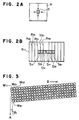
- the DMD 2 includes, as illustrated in Fig. 1B, a multiplicity of mirrors M each formed in a square having a side length L which is 16 ⁇ m in the present embodiment. Respective adjacent mirrors are spaced by a gap set at 1 ⁇ m.
- Each mirror M is structured such that a movable end Mb swings about the diagonal connecting two fixed ends Ma to incline the reflecting surface. In the example illustrated in Fig. 1B, the movable end Mb swings upon receiving an electrostatic force induced by an electric field generated at an electrode on a substrate, not shown.
- Fig. 1C illustrates an array of mirrors M of the DMD 2 viewed through from the rear side of the DMD 2.
- n 6
- the respective mirror columns are shifted by p/n (approximately 2.8 ⁇ m) from the preceding and/or subsequent ones in the orthogonal direction.
- the microlens 3 includes a plurality of lenses, each of which converges reflected light from a reflecting surface R of a corresponding one of the mirrors M to irradiate the object 5 with a reflected light image in the form of a spot S having the size of one pixel.
- the characteristic of the microlens 3 is set such that the spot S has one side equal to the above-mentioned shift amount p/n (approximately 2.8 ⁇ m) and an area approximately 1/36 the reflecting surface.
- the microlens 3 may be implemented, for example, by an equivalent of a microlens used to converge light onto each of light receiving elements on a sensing surface of an imaging device such as CCD or the like.
- the controller 4 includes an image data processing unit and a mirror drive control unit.
- the image data processing unit generates time-series drive control data for controlling and driving the respective mirrors of the DMD 2 based on image data sent thereto from an external computer, image data generated by reading an original through a scanner, or the like.
- the mirror drive control unit of the controller controls the inclination of the reflecting surface of each mirror in the DMD 2 in the following manner based on the drive control data generated by the image data processing unit.
- description is made on how to control pixels in the first line of a light image formed on an object.
- reflected light from a second mirror column M2i ( i 1 to m ) in Fig.
- the DMD 2 is controlled to repeat the foregoing irradiation for the remaining mirror columns to form the object with pixels Sl1 - S61, S12 - S62, and so on, aligned in the orthogonal direction B, as illustrated in Fig. 2B (illustration of pixels S12 - S62, and so on are omitted in Fig. 2B).
- the second and subsequent lines are formed by similarly controlling the DMD 2.
- the optical image forming device can significantly enhance the pixel density of a light image formed on the object 5 without increasing the number of mirrors in the orthogonal direction.
- the pixel density in the example illustrated in Figs. 1 and 2 is enhanced at a stretch six (equal to the number of mirror columns) times as high as that of a light image which may be formed by irradiating an object with reflected light from one mirror column without changing its area.
- reflected light from the respective mirrors M can be effectively utilized to enhance the intensity of irradiated light at each pixel, as compared with the use of only a portion of reflecting surfaces of the respective mirrors in the DMD 2.
- the DMD 2 may be formed of an array of mirrors, each of which has the longitudinal direction inclined by a predetermined angle ⁇ 1 with respect to the orthogonal direction B as illustrated in Fig. 3.
- a DMD 2 includes n mirror columns arranged in the direction orthogonal to the longitudinal direction, each of which includes m mirrors arranged in the longitudinal direction with a pitch p, thus configuring the mirrors in the form of (mxn) array.
- the respective mirrors in the DMD 2 are controlled such that reflected light images therefrom are aligned in the orthogonal direction B.
- the mirrors constituting the DMD 2 used in this embodiment are not limited in shape and size to a square having a side length of 16 ⁇ m, as mentioned above, but may be varied depending on restrictions possibly imposed by a manufacturing process of the DMD 2, the whole configuration of the optical image forming device, or the like.
- a light image irradiated to the object 5 may be optionally enlarged or reduced in general depending on the size of the object 5.
- the angle ⁇ 2 formed by the optical axis of incident light to the DMD 2 and the optical axis of light emitted from the DMD 2 is preferably as small as possible, as illustrated in Eig. 4, to reduce variations in the distance between each of the mirrors and a corresponding lens in the microlens 3 in order to prevent the light image from each mirror from being out of focus on the object. Also, as illustrated in Fig.
- the DMD 2, the microlens 3 and the irradiated surface of the object 5 may be arranged in parallel with each other with the angle ⁇ 2 maintained at approximately 90°, so as to eliminate variations in the distance between each mirror and a corresponding lens in the microlens 3 and in the distance between each lens and the irradiated surface of the object 5. Furthermore, the configurations illustrated in Figs. 4 and 5 may be combined.
- FIG. 6 schematically illustrates the configuration of a printer according to this embodiment, wherein parts similar to those in Fig. 1A of the foregoing Embodiment 1 are designated the same reference numerals, and explanation thereon is omitted.
- a drum-shaped photosensitive material 10 serving as an image carrier rotated in a direction indicated by an arrow C, is uniformly charged by a charger 11, and exposed to a light image from the DMD 2 which is controlled on the basis of image data sent from an external device such as a personal computer.
- an electrostatic latent image is formed on the photosensitive material 10.
- the electrostatic latent image on the photosensitive material 10 is developed into a toner image as supplied toner particles selectively attach thereto in a developer 12.
- the toner image on the photosensitive material 10 is transferred to a transfer sheet 14 as a transfer material by a transfer unit 13.
- the axial direction of the photosensitive material corresponds to the orthogonal direction B.
- the size, number and so on of mirrors M in the DMD 2 are set based on the width of an image in the axial direction of the photosensitive material 10, and an intended pixel density. Assuming for example that an image having a width of 200 mm in the axial direction of the photosensitive material 10 is formed at an intended pixel density of 1200 dpi (dot per inch), the DMD 2 will have approximately 9,450 pixels in the width direction of the image.
- the microlens 3 it is possible, by use of the microlens 3, to enhance the intensity of irradiated light on each of pixels of a light image irradiated to the photosensitive material 10, increase a speed at which an electrostatic latent image is formed on the photosensitive material 10, and transfer an image having a high image density to the transfer sheet 14 to form the image thereon.
- FIG. 7 schematically illustrates the configuration of an aligner according to this embodiment, where parts similar to those in the aforementioned Embodiment 1 illustrated in Fig. 1A are designated the same reference numerals, and explanation thereon is omitted.
- a substrate 15 having a photoresist layer 15a formed on the surface thereof is supported on a stage 16 which is driven in a direction indicated by an arrow D.
- the DMD 2 is controlled to form a target pattern based on digital information data, while the stage 16 is driven in the direction indicated by the arrow D, thereby fully exposing the photoresist layer 15a on the substrate 15.
- the photoresist pattern 15a on the substrate 15 is developed to form a predetermined resist pattern on the substrate 15.
- the microlens 3 it is possible, by use of the microlens 3, to enhance the intensity of irradiated light on each of pixels on the photoresist layer 15a, increase a speed at which the photoresist layer 15a is exposed, and form a resist pattern having a high line density on the substrate 15.
- the optical image forming device is applied to the formation of a resist pattern on a substrate, it can also be applied to an aligner such as a so-called stepper for use in the formation of a resist pattern for forming a large number of integrated circuit devices on a semiconductor wafer serving as a substrate.
Abstract
Description
- The present invention relates generally to an optical image forming method and device for forming a light image on an object, and more particularly to an optical image forming method and device for forming a light image on an object which moves in one direction relative to reflected light irradiated thereto from a spatial light modulator including a plurality of mirrors each capable of independently controlling the inclination of its reflecting surface, as well as to a printer, an image forming apparatus such as a copying machine, and an aligner for lithography, all of which may utilize the device.
- Conventionally, a device named a digital micromirror device (hereinafter referred to as the "DMD") is known as a spatial light modulator of the type mentioned above. Specifically, the DMD has a multiplicity of micromirrors, referred to as micromirrors, each rotatable about a fixed axis, formed on a semiconductor substrate of Si or the like. The DMD is irradiated with light from a light source which is deflected by each of the micromirrors, the rotation of which is controlled by an electrostatic action or the like. Each of the micromirrors is selectively rotated to change the inclination of its reflecting surface to selectively irradiate an object with reflected light from each of the micromirrors to form a light image on the object.
- Originally, the DMD has been proposed for applications in a display such as a digital large screen projector or the like. Recently, however, applications proposed for the DMD have been increasingly directed to an optical writing system for writing a laser beam onto a photosensitive material in an image forming apparatus such as an electrophotographic printer, as described in, for example, Laid-open Japanese Patent Applications Nos. 8-318641, 7-232458 and 9-300701. Particularly, the Application No. 8-318641 describes a method of forming all pixels in the axial direction of a photosensitive material using a DMD having a small number of mirrors and a reduced device length in the axial direction (longitudinal direction). Specifically, the DMD is composed of a plurality of mirror columns arranged in a direction in which the surface of a photosensitive material, as an object, is moved, wherein each of the mirror columns includes a plurality of mirrors arranged in an axial direction, orthogonal to the surface moving direction, and effective reflecting surfaces of mirrors in each mirror column are shifted in the axial direction, so that one line portion of a light image on a photosensitive material is formed using the plurality of mirror columns of the DMD.
- In the method disclosed in the above-mentioned Laid-open Japanese Patent Application No. 8-318641, the object is irradiated only with a portion of reflected light from each mirror in order to prevent reflected light images of the respective mirrors from overlapping with each other in the direction orthogonal to the direction of the relative movement of the object, so that the irradiating light having only a reduced intensity reaches each of pixels on the object (photosensitive material). This also leads to a requirement for a technique of irradiating respective pixels with reflected light from the mirrors a plurality of times.
- On the other hand, while the pixel density tends to be higher in the field of modern image forming apparatus or the like, the present inventors have found that the pixel density can be significantly improved in the formation of a light image on an object such as a photosensitive material even without the need for increasing the number of mirrors in the direction orthogonal to the direction of the relative movement of the object in a spatial light modulator such as the above-mentioned DMD.
- The present invention has been made in view of the problems mentioned above, and its object is to provide an optical image forming method and device which are capable of forming a light image in a high pixel density and of enhancing the intensity of light irradiated to each pixel by effectively utilizing reflected light from respective mirrors of a spatial light modulator. Another object of the present invention is to provide an image forming apparatus and an aligner for lithography using the device.
- To achieve the above objects, in a first aspect, the present invention provides an optical image forming method for forming a light image on an object which includes the steps of irradiating light from a light source to a spatial light modulator including a plurality of mirrors, wherein each of the mirrors is capable of independently controlling the inclination of a reflecting surface thereof, irradiating reflected light from the spatial light modulator to an object which moves in one direction relative to the reflected light, arranging the respective mirrors of the spatial light modulator to reflect light therefrom such that reflected light images from the mirrors of the spatial light modulator are aligned on the object in a direction orthogonal to the direction of the relatively movement with a pitch smaller than the pitch p of the mirrors, and converging reflected light from the respective mirrors of the spatial light modulator onto the object.
- In this optical image forming method, reflected light images from the mirrors of the spatial light modulator are aligned on the object in the direction orthogonal to the direction of the relative movement with a pitch smaller than the pitch p of the mirrors, and reflected light from each of the mirrors of the spatial light modulator is converged onto the object, thereby forming a light image at a high pixel density on the object. Here, the reflected light from the respective mirrors of the spatial light modulator is converged onto the object to effectively utilize the reflected light from the respective mirrors, thereby enhancing the intensity of irradiated light in respective pixels.
- In a second aspect, the present invention provides an optical image forming device for forming a light image on an object, which includes a light source, a spatial light modulator including a plurality of mirrors, each of which is capable of independently controlling the inclination of a reflecting surface thereof for reflecting light from the light source, wherein reflected light from the spatial light modulator is irradiated to an object which moves in one direction relative to the reflected light, a controller which controls the inclination of the reflecting surface of each of the mirrors such that reflected light images from the respective mirrors of the spatial light modulator are aligned on the object in a direction orthogonal to the direction of the relative movement with a pitch smaller than the pitch p of the mirrors, and a plurality of lenses each for converging reflected light from a corresponding mirror of the spatial light modulator onto the object.
- In the optical image forming device, the respective mirrors are arranged at predetermined positions, and the controller controls the inclination of the reflecting surface of each of the mirrors such that reflected light images from the respective mirrors of the spatial light modulator are aligned on the object in a direction orthogonal to the direction of the relative movement with a pitch smaller than the pitch p of the mirrors. Then, the reflected light from the respective mirrors is converged onto the object by the plurality of lenses to form a light image at a high pixel density on the object. In this event, the reflected light from the respective mirrors is converged by the lenses to effectively utilize the reflected light from the respective mirrors, thereby enhancing the intensity of irradiated light in respective pixels.
- The reflected light from the respective mirrors may be converged on the object in such a degree to prevent overlapping, or may be converged to permit slight overlapping.
- The spatial light modulator may include n mirror columns arranged in the direction of the relative movement, wherein each of the mirror columns is composed of m mirrors arranged with the pitch p in the direction orthogonal to the direction of the relative movement, and the mirror columns are arranged with an offset in the direction orthogonal to the direction of the relative movement. In this embodiment, the controller may control the inclination of the reflecting surface of each of the mirrors, such that reflected light images from the respective mirrors are aligned in the direction orthogonal to the direction of the relative movement.
- The n mirror columns, arranged in the direction of the relative movement, are each composed of m mirrors arranged with the pitch p in the direction orthogonal to the direction of the relative movement, wherein the mirror columns are arranged with an offset in the direction orthogonal to the direction of the relative movement, such that the reflected light image from the respective mirrors are arranged in the direction orthogonal to the direction of the relative movement. Then, the controller controls the inclination of the reflecting surface of each of the mirrors, such that reflected light images from the respective mirrors are aligned in the direction orthogonal to the direction of the relative movement.
- Also, the spatial light modulator may include n mirror columns arranged in a longitudinal direction of the spatial light modulator, wherein each of the mirror columns includes m mirrors arranged with the pitch p in the longitudinal direction, to form an array of (mxn) mirrors which constitute the spatial light modulator, and the longitudinal direction of the spatial light modulator is inclined with respect to the direction orthogonal to the direction of the relative movement, so as to sequentially shift the position at which a reflected light image reflected off an ith mirror (
- Each of the n mirror columns, arranged in the longitudinal direction of the spatial light modulator, includes m mirrors arranged with the pitch p in a longitudinal direction of the spatial light modulator, to form an array of (mxn) mirrors constituting the spatial light modulator, wherein the longitudinal direction of the spatial light modulator is inclined with respect to the direction orthogonal to the direction of the relative movement, so as to sequentially shift the position at which a reflected light image reflected off an ith mirror (
- The pitch with which the reflected light images from the respective mirrors are arranged in the direction orthogonal to the direction of the relative movement may be set at the value of (p/n). Alternatively, the pitch may be set at any appropriate value.
- In a third aspect, the present invention provides an image forming apparatus including a latent image forming mechanism which irradiates a light image to a uniformly charged image carrier to form a latent image, a developing mechanism which develops the latent image on the image carrier to form an actual image, and a transfer mechanism which transfers the actual image on the image carrier onto a transfer material, wherein the aforementioned optical image forming device is used as the latent image forming mechanism.
- In the image forming apparatus, reflected light from the respective mirrors of the spatial light modulator is converged by the lenses to irradiate the uniformly charged image carrier with the converged light, thereby making it possible to enhance the intensity of the irradiated light to each pixel and to form a latent image at a high pixel density on the image carrier.
- In a fourth aspect, the present invention provides an aligner for lithography for irradiating a light image to a substrate having a photoresist layer formed on a surface thereof, including the aforementioned optical image forming device for irradiating the substrate with a light image.
- In the aligner for lithography, reflected light from the respective mirrors of the spatial light modulator is converged by the lenses to irradiate the converged light to the surface of the substrate having the photoresist layer formed thereon, thereby making it possible to enhance the intensity of the irradiated light to each pixel and to form a resist pattern at a high pixel density on the substrate.
- Other objects, features, and advantages of the present invention will become apparent from the following detailed description when read in conjunction with the accompanying drawings.
- A more complete appreciation of the present invention and many of the attendant advantages thereof will be readily obtained as the same becomes better understood by reference to the following detailed description when considered in connection with the accompanying drawings, wherein:
- Fig. 1A is a schematic diagram illustrating an optical image forming device according to a first embodiment of the present invention;
- Fig. 1B is a schematic diagram illustrating the shape of mirrors constituting a DMD in the optical image forming device of Fig. 1A;
- Fig. 1C is a diagram illustrating the arrangement of mirrors in the DMD;
- Fig. 2A is a schematic diagram illustrating the relationship between a reflecting surface R of a mirror in the DMD and a pixel spot S on an object;
- Fig. 2B is a schematic diagram illustrating columns of pixels formed on an object;
- Fig. 3 is a schematic diagram illustrating the arrangement of mirrors in the DMD according to a modified example;
- Fig. 4 is a schematic diagram illustrating positioning of a microlens and an object according to a modified example;
- Fig. 5 is a schematic diagram illustrating positioning of a microlens and an object according to another modified example;
- Fig. 6 is a schematic diagram illustrating the configuration of a printer according to a second embodiment; and
- Fig. 7 is a schematic diagram illustrating the configuration of an aligner for lithography according to a third embodiment.
-
- Several embodiments of the present invention will hereinafter be described with reference to the accompanying drawings.
- Fig. 1A schematically illustrates the structure of an optical image forming device which can embody an optical image forming method according to the present invention. The illustrated device includes a light source 1; a digital micromirror device (DMD) 2 including a plurality of mirrors each capable of independently controlling the inclination of its reflecting surface and serving as a spatial light modulator; a
microlens 3 including a plurality of miniature lenses for converging reflected light from respective mirrors of theDMD 2 onto a light image forming object (hereinafter referred to as the "object") 5 which moves in a direction indicated by an arrow A; and acontroller 4 which controls the inclination of the reflecting surface of each mirror in theDMD 2 based on image data. - The light source 1 may be implemented by a light emitting diode, a laser or the like, other than an ordinary lamp. In the example illustrated in Fig. 1A, light from the light source 1 is transformed into substantially a parallel beam through a
collimator lens 6, and is irradiated to a mirror surface of theDMD 2. A slit may be inserted between the light source 1 and theDMD 2 as required. - The
DMD 2 includes, as illustrated in Fig. 1B, a multiplicity of mirrors M each formed in a square having a side length L which is 16 µm in the present embodiment. Respective adjacent mirrors are spaced by a gap set at 1 µm. Each mirror M is structured such that a movable end Mb swings about the diagonal connecting two fixed ends Ma to incline the reflecting surface. In the example illustrated in Fig. 1B, the movable end Mb swings upon receiving an electrostatic force induced by an electric field generated at an electrode on a substrate, not shown. - Fig. 1C illustrates an array of mirrors M of the
DMD 2 viewed through from the rear side of theDMD 2. Referring specifically to Fig. 1C, there are n mirror columns (here n=6) arranged in a direction in which theobject 5 is moved. Each mirror column includes m (representing the range of several hundreds) mirrors arranged with a pitch p (=17 µm) in the direction orthogonal to the moving direction of the object 5 (hereinafter referred to as the "orthogonal direction" and indicated by an arrow B in Fig. 1C). Also, the respective mirror columns are shifted by p/n (approximately 2.8 µm) from the preceding and/or subsequent ones in the orthogonal direction. - The
microlens 3 includes a plurality of lenses, each of which converges reflected light from a reflecting surface R of a corresponding one of the mirrors M to irradiate theobject 5 with a reflected light image in the form of a spot S having the size of one pixel. The characteristic of themicrolens 3 is set such that the spot S has one side equal to the above-mentioned shift amount p/n (approximately 2.8 µm) and an area approximately 1/36 the reflecting surface. Themicrolens 3 may be implemented, for example, by an equivalent of a microlens used to converge light onto each of light receiving elements on a sensing surface of an imaging device such as CCD or the like. - The
controller 4 includes an image data processing unit and a mirror drive control unit. The image data processing unit generates time-series drive control data for controlling and driving the respective mirrors of theDMD 2 based on image data sent thereto from an external computer, image data generated by reading an original through a scanner, or the like. - The mirror drive control unit of the
controller 4, in turn, controls the inclination of the reflecting surface of each mirror in theDMD 2 in the following manner based on the drive control data generated by the image data processing unit. In the following, description is made on how to control pixels in the first line of a light image formed on an object. First, reflected light from a first mirror column M1i (object 5. Next, reflected light from a second mirror column M2i (object 5 in a similar manner at timing after a time equal to the pitch p' of pixels on theobject 5 divided by a moving speed V of the object 5 (p'/V). TheDMD 2 is controlled to repeat the foregoing irradiation for the remaining mirror columns to form the object with pixels Sl1 - S61, S12 - S62, and so on, aligned in the orthogonal direction B, as illustrated in Fig. 2B (illustration of pixels S12 - S62, and so on are omitted in Fig. 2B). The second and subsequent lines are formed by similarly controlling theDMD 2. - In this way, the optical image forming device according to Embodiment 1 can significantly enhance the pixel density of a light image formed on the
object 5 without increasing the number of mirrors in the orthogonal direction. The pixel density in the example illustrated in Figs. 1 and 2 is enhanced at a stretch six (equal to the number of mirror columns) times as high as that of a light image which may be formed by irradiating an object with reflected light from one mirror column without changing its area. - In addition, reflected light from the respective mirrors M can be effectively utilized to enhance the intensity of irradiated light at each pixel, as compared with the use of only a portion of reflecting surfaces of the respective mirrors in the
DMD 2. - It should be noted that while this embodiment employs the
DMD 2 which is formed of the mirror columns sequentially shifted in the orthogonal direction, theDMD 2 may be formed of an array of mirrors, each of which has the longitudinal direction inclined by a predetermined angle 1 with respect to the orthogonal direction B as illustrated in Fig. 3. Referring specifically to Fig. 3, aDMD 2 includes n mirror columns arranged in the direction orthogonal to the longitudinal direction, each of which includes m mirrors arranged in the longitudinal direction with a pitch p, thus configuring the mirrors in the form of (mxn) array. Then, the inclination angle 1 of theDMD 2 is set such that the position at which a reflected light image reflected off an ith mirror (DMD 2 are controlled such that reflected light images therefrom are aligned in the orthogonal direction B. - Also, the mirrors constituting the
DMD 2 used in this embodiment are not limited in shape and size to a square having a side length of 16 µm, as mentioned above, but may be varied depending on restrictions possibly imposed by a manufacturing process of theDMD 2, the whole configuration of the optical image forming device, or the like. - Further, in this embodiment, a light image irradiated to the
object 5 may be optionally enlarged or reduced in general depending on the size of theobject 5. - Further, in this embodiment, the angle 2 formed by the optical axis of incident light to the
DMD 2 and the optical axis of light emitted from theDMD 2 is preferably as small as possible, as illustrated in Eig. 4, to reduce variations in the distance between each of the mirrors and a corresponding lens in themicrolens 3 in order to prevent the light image from each mirror from being out of focus on the object. Also, as illustrated in Fig. 5, theDMD 2, themicrolens 3 and the irradiated surface of theobject 5 may be arranged in parallel with each other with the angle 2 maintained at approximately 90°, so as to eliminate variations in the distance between each mirror and a corresponding lens in themicrolens 3 and in the distance between each lens and the irradiated surface of theobject 5. Furthermore, the configurations illustrated in Figs. 4 and 5 may be combined. - Next, description will be made on an exemplary application for the
DMD 2 which is employed in a printer serving as an image forming device. Fig. 6 schematically illustrates the configuration of a printer according to this embodiment, wherein parts similar to those in Fig. 1A of the foregoing Embodiment 1 are designated the same reference numerals, and explanation thereon is omitted. - Referring specifically to Fig. 6, the surface of a drum-shaped
photosensitive material 10, serving as an image carrier rotated in a direction indicated by an arrow C, is uniformly charged by acharger 11, and exposed to a light image from theDMD 2 which is controlled on the basis of image data sent from an external device such as a personal computer. In this way, an electrostatic latent image is formed on thephotosensitive material 10. The electrostatic latent image on thephotosensitive material 10 is developed into a toner image as supplied toner particles selectively attach thereto in adeveloper 12. The toner image on thephotosensitive material 10 is transferred to atransfer sheet 14 as a transfer material by atransfer unit 13. - Thus, when the
aforementioned DMD 2 is applied to a printer for forming an image on atransfer sheet 14, the axial direction of the photosensitive material corresponds to the orthogonal direction B. The size, number and so on of mirrors M in theDMD 2 are set based on the width of an image in the axial direction of thephotosensitive material 10, and an intended pixel density. Assuming for example that an image having a width of 200 mm in the axial direction of thephotosensitive material 10 is formed at an intended pixel density of 1200 dpi (dot per inch), theDMD 2 will have approximately 9,450 pixels in the width direction of the image. Thus, employing theDMD 2 illustrated in Fig. 1C, a required number of mirrors m in each mirror column is approximately 788 when theDMD 2 has 12 mirror columns (n=12), and a required number of mirrors m in each mirror column is approximately 148 when theDMD 2 has 64 mirror columns (n=64). If the length of theDMD 2 in the longitudinal direction does not match the width of an image, a light image irradiated from theDMD 2 may be enlarged or reduced as the case may be. - According to this embodiment, it is possible, by use of the
microlens 3, to enhance the intensity of irradiated light on each of pixels of a light image irradiated to thephotosensitive material 10, increase a speed at which an electrostatic latent image is formed on thephotosensitive material 10, and transfer an image having a high image density to thetransfer sheet 14 to form the image thereon. - Next, description will be made on an exemplary application for the
DMD 2 which is applied to an aligner for lithography. Fig. 7 schematically illustrates the configuration of an aligner according to this embodiment, where parts similar to those in the aforementioned Embodiment 1 illustrated in Fig. 1A are designated the same reference numerals, and explanation thereon is omitted. - Referring specifically to Fig. 7, a
substrate 15 having aphotoresist layer 15a formed on the surface thereof is supported on astage 16 which is driven in a direction indicated by an arrow D. TheDMD 2 is controlled to form a target pattern based on digital information data, while thestage 16 is driven in the direction indicated by the arrow D, thereby fully exposing thephotoresist layer 15a on thesubstrate 15. Subsequently, thephotoresist pattern 15a on thesubstrate 15 is developed to form a predetermined resist pattern on thesubstrate 15. - According to this embodiment, it is possible, by use of the
microlens 3, to enhance the intensity of irradiated light on each of pixels on thephotoresist layer 15a, increase a speed at which thephotoresist layer 15a is exposed, and form a resist pattern having a high line density on thesubstrate 15. - While in this embodiment, the optical image forming device is applied to the formation of a resist pattern on a substrate, it can also be applied to an aligner such as a so-called stepper for use in the formation of a resist pattern for forming a large number of integrated circuit devices on a semiconductor wafer serving as a substrate.
- In describing preferred embodiments of the present invention illustrated in the drawings, specific terminology is employed for the sake of clarity. However, the present invention is not intended to be limited to the specific terminology so selected and it is to be understood that each specific element includes all technical equivalents which operate in a similar manner.
Claims (6)
- An optical image forming method for forming a light image on an object, comprising the steps of:irradiating light from a light source to a spatial light modulator including a plurality of mirrors, each of said mirrors capable of independently controlling the inclination of a reflecting surface thereof;irradiating reflected light from said spatial light modulator to an object which moves in one direction relative to said reflected light;arranging said respective mirrors of said spatial light modulator to reflect light therefrom such that reflected light images from said mirrors of said spatial light modulator are aligned on said object in a direction orthogonal to the direction of the relative movement of said object with a pitch smaller than the pitch p of said mirrors; andconverging said reflected light from said respective mirrors of said spatial light modulator onto said object.
- An optical image forming device for forming a light image on an object, said device comprising:a light source;a spatial light modulator including a plurality of mirrors, each of said mirrors capable of independently controlling the inclination of a reflecting surface thereof for reflecting light from said light source, wherein reflected light from said spatial light modulator is irradiated to an object which moves in one direction relative to said reflected light;a controller which controls the inclination of the reflecting surface of each of said mirrors such that reflected light images from said respective mirrors of said spatial light modulator are aligned on said object in a direction orthogonal to the direction of the relative movement with a pitch smaller than the pitch p of said mirrors; anda plurality of lenses each for converging reflected light from a corresponding mirror of said spatial light modulator onto said object.
- An optical image forming device according to claim 2, wherein:said spatial light modulator includes n mirror columns arranged in the direction of the relative movement, each of said mirror columns including m mirrors arranged with the pitch p in the direction orthogonal to the direction of the relative movement, said mirror columns being arranged with an offset in the direction orthogonal to the direction of the relative movement; andsaid controller controls the inclination of the reflecting surface of each of said mirrors, such that reflected light images from said respective mirrors are aligned in the direction orthogonal to the direction of the relative movement.
- An optical image forming device according to claim 2, wherein:said spatial light modulator includes n mirror columns arranged in a longitudinal direction of said spatial light modulator, each of said mirror columns including m mirrors arranged with the pitch p in the longitudinal direction, to form an array of (mxn) mirrors which constitute said spatial light modulator;the longitudinal direction of said spatial light modulator is inclined with respect to the direction orthogonal to the direction of the relative movement, so as to sequentially shift the position at which a reflected light image reflected off an ith mirror, wherein i varies 1 to m, in each of said mirror columns is formed in the direction orthogonal to the direction of the relative movement; andsaid controller controls the inclination of the reflecting surface of each of said mirrors such that reflected light images from said respective mirrors are aligned in the direction orthogonal to the direction of the relative movement.
- An image forming apparatus, comprising:a latent image forming mechanism which irradiates a light image to a uniformly charged image carrier to form a latent image;Xa developing mechanism which develops the latent image on said image carrier to form an actual image; anda transfer mechanism which transfers the actual image on said image carrier onto a transfer material,an optical image forming device which comprises:a light source;a spatial light modulator including a plurality of mirrors, each of said mirrors capable of independently controlling the inclination of a reflecting surface thereof for reflecting light from said light source, wherein reflected light from said spatial light modulator is irradiated to an object which moves in one direction relative to said reflected light;a controller which controls the inclination of the reflecting surface of each of said mirrors such that reflected light images from said respective mirrors of said spatial light modulator are aligned on said object in a direction orthogonal to the direction of the relative movement with a pitch smaller than the pitch p of said mirrors; anda plurality of lenses each for converging reflected light from a corresponding mirror of said spatial light modulator onto said object.
- An aligner for lithography for irradiating a light image to a substrate having a photoresist layer formed on a surface thereof, said aligner comprising an optical image forming device which comprises:a light source;a spatial light modulator including a plurality of mirrors, each of said mirrors capable of independently controlling the inclination of a reflecting surface thereof for reflecting light from said light source, wherein reflected light from said spatial light modulator is irradiated to an object which moves in one direction relative to said reflected light;a controller which controls the inclination of the reflecting surface of each of said mirrors such that reflected light images from said respective mirrors of said spatial light modulator are aligned on said object in a direction orthogonal to the direction of the relative movement with a pitch smaller than the pitch p of said mirrors; anda plurality of lenses each for converging reflected light from a corresponding mirror of said spatial light modulator onto said object.
Applications Claiming Priority (2)
| Application Number | Priority Date | Filing Date | Title |
|---|---|---|---|
| JP14844998A JPH11320968A (en) | 1998-05-13 | 1998-05-13 | Optical image forming method and apparatus, imaging system and exposing unit for lithography |
| JP14844998 | 1998-05-13 |
Publications (2)
| Publication Number | Publication Date |
|---|---|
| EP0957384A2 true EP0957384A2 (en) | 1999-11-17 |
| EP0957384A3 EP0957384A3 (en) | 2000-10-04 |
Family
ID=15453042
Family Applications (1)
| Application Number | Title | Priority Date | Filing Date |
|---|---|---|---|
| EP99108639A Withdrawn EP0957384A3 (en) | 1998-05-13 | 1999-05-12 | Optical image forming method and device, image forming apparatus and aligner for lithography |
Country Status (3)
| Country | Link |
|---|---|
| US (1) | US6288830B1 (en) |
| EP (1) | EP0957384A3 (en) |
| JP (1) | JPH11320968A (en) |
Cited By (7)
| Publication number | Priority date | Publication date | Assignee | Title |
|---|---|---|---|---|
| EP2561992A3 (en) * | 2011-08-24 | 2014-01-22 | Palo Alto Research Center Incorporated | Single-Pass Imaging System Using Spatial Light Modulator and Anamorphic Projection Optics |
| EP2561993A3 (en) * | 2011-08-24 | 2014-01-22 | Palo Alto Research Center Incorporated | Single-pass imaging system using spatial light modulator and anamorphic projection optics |
| US8767270B2 (en) | 2011-08-24 | 2014-07-01 | Palo Alto Research Center Incorporated | Single-pass imaging apparatus with image data scrolling for improved resolution contrast and exposure extent |
| US8791972B2 (en) | 2012-02-13 | 2014-07-29 | Xerox Corporation | Reflex-type digital offset printing system with serially arranged single-pass, single-color imaging systems |
| US8872875B2 (en) | 2011-08-24 | 2014-10-28 | Palo Alto Research Center Incorporated | Single-pass imaging system with anamorphic optical system |
| US9354379B2 (en) | 2014-09-29 | 2016-05-31 | Palo Alto Research Center Incorporated | Light guide based optical system for laser line generator |
| US9630424B2 (en) | 2011-08-24 | 2017-04-25 | Palo Alto Research Center Incorporated | VCSEL-based variable image optical line generator |
Families Citing this family (28)
| Publication number | Priority date | Publication date | Assignee | Title |
|---|---|---|---|---|
| US6969635B2 (en) * | 2000-12-07 | 2005-11-29 | Reflectivity, Inc. | Methods for depositing, releasing and packaging micro-electromechanical devices on wafer substrates |
| JP2001188354A (en) * | 1999-12-28 | 2001-07-10 | Asahi Kasei Corp | Method for manufacturing photosensitive resin letterpress and apparatus for manufacturing the same |
| JP2001330912A (en) * | 2000-05-18 | 2001-11-30 | Fuji Photo Film Co Ltd | Image recording device |
| US7172296B2 (en) * | 2000-08-30 | 2007-02-06 | Reflectivity, Inc | Projection display |
| JP2002072491A (en) * | 2000-09-01 | 2002-03-12 | Airex Inc | Printed circuit board manufacturing apparatus |
| JP5144863B2 (en) * | 2001-06-29 | 2013-02-13 | 株式会社オーク製作所 | Multiple exposure drawing method and multiple exposure drawing apparatus |
| JP4728536B2 (en) * | 2001-07-05 | 2011-07-20 | 株式会社オーク製作所 | Multiple exposure drawing method and multiple exposure drawing apparatus |
| KR20030059705A (en) * | 2002-01-04 | 2003-07-10 | 엘지전자 주식회사 | A photo maskless facing exposure |
| KR100452852B1 (en) * | 2002-01-09 | 2004-10-14 | 삼성전자주식회사 | imaging optical system and image forming apparatus having the same |
| KR20040102089A (en) * | 2002-04-15 | 2004-12-03 | 코닌클리케 필립스 일렉트로닉스 엔.브이. | Imaging method |
| JP3938714B2 (en) * | 2002-05-16 | 2007-06-27 | 大日本スクリーン製造株式会社 | Exposure equipment |
| JP4201178B2 (en) | 2002-05-30 | 2008-12-24 | 大日本スクリーン製造株式会社 | Image recording device |
| EP1573366B1 (en) * | 2002-08-24 | 2016-11-09 | Chime Ball Technology Co., Ltd. | Continuous direct-write optical lithography |
| KR100480620B1 (en) * | 2002-09-19 | 2005-03-31 | 삼성전자주식회사 | Exposing equipment including a Micro Mirror Array and exposing method using the exposing equipment |
| JP2004287082A (en) * | 2003-03-20 | 2004-10-14 | Tadahiro Omi | Mask drawing apparatus |
| JP2004264337A (en) * | 2003-01-28 | 2004-09-24 | Tadahiro Omi | Method for forming mask and mask forming apparatus |
| JP2005056995A (en) * | 2003-08-01 | 2005-03-03 | Tadahiro Omi | Pattern drawing method and apparatus |
| ATE404907T1 (en) * | 2003-08-27 | 2008-08-15 | Koninkl Philips Electronics Nv | METHOD FOR GENERATING OPTICAL IMAGES, DEVICE FOR CARRYING OUT THE METHOD AND PROCESS FOR PRODUCING A COMPONENT USING THE METHOD |
| US7218336B2 (en) * | 2003-09-26 | 2007-05-15 | Silicon Light Machines Corporation | Methods and apparatus for driving illuminators in printing applications |
| JP4638826B2 (en) * | 2005-02-04 | 2011-02-23 | 富士フイルム株式会社 | Drawing apparatus and drawing method |
| JP4410134B2 (en) * | 2005-03-24 | 2010-02-03 | 日立ビアメカニクス株式会社 | Pattern exposure method and apparatus |
| JP2007025394A (en) * | 2005-07-19 | 2007-02-01 | Fujifilm Holdings Corp | Pattern forming method |
| JP2007086373A (en) * | 2005-09-21 | 2007-04-05 | Fujifilm Corp | Permanent pattern forming method |
| US7782524B2 (en) * | 2007-10-02 | 2010-08-24 | Silicon Quest Kabushiki-Kaisha | System configurations and methods for controlling image projection apparatuses |
| US20090111062A1 (en) * | 2007-10-30 | 2009-04-30 | Hitachi Via Mechanics, Ltd. | Pattern Formation Method |
| JP5219982B2 (en) * | 2009-11-20 | 2013-06-26 | 株式会社日立ハイテクノロジーズ | Exposure apparatus, exposure method, and manufacturing method of display panel substrate |
| JP6146646B2 (en) * | 2012-12-27 | 2017-06-14 | 大日本印刷株式会社 | Illumination device, projection device, scanner and exposure device |
| CN112838018B (en) * | 2019-11-25 | 2023-09-15 | 致茂电子(苏州)有限公司 | Optical measuring method |
Citations (3)
| Publication number | Priority date | Publication date | Assignee | Title |
|---|---|---|---|---|
| JPH07232458A (en) | 1993-08-30 | 1995-09-05 | Texas Instr Inc <Ti> | Method and device for printing stroke data with continuous gradation data |
| JPH08318641A (en) | 1995-04-19 | 1996-12-03 | Texas Instr Inc <Ti> | Method and system for independently illuminating more than one area of object |
| JPH09300701A (en) | 1995-10-25 | 1997-11-25 | Texas Instr Inc <Ti> | Illumination system for hard copy device |
Family Cites Families (20)
| Publication number | Priority date | Publication date | Assignee | Title |
|---|---|---|---|---|
| US4393387A (en) * | 1979-09-14 | 1983-07-12 | Canon Kabushiki Kaisha | Beam recording apparatus effecting the recording by a plurality of beams |
| GB2123247B (en) * | 1982-07-02 | 1986-01-22 | Xerox Corp | Facsimile reproduction scanner |
| US4842396A (en) | 1984-06-29 | 1989-06-27 | Canon Kabushiki Kaisha | Light modulation element and light modulation apparatus |
| US5061049A (en) * | 1984-08-31 | 1991-10-29 | Texas Instruments Incorporated | Spatial light modulator and method |
| US4940314A (en) * | 1985-05-13 | 1990-07-10 | Xerox Corporation | Variable wavelength discrete optical image bars having passively enhanced spatial addressing capacity |
| US5028939A (en) * | 1988-08-23 | 1991-07-02 | Texas Instruments Incorporated | Spatial light modulator system |
| US5041851A (en) * | 1989-12-21 | 1991-08-20 | Texas Instruments Incorporated | Spatial light modulator printer and method of operation |
| US5083857A (en) * | 1990-06-29 | 1992-01-28 | Texas Instruments Incorporated | Multi-level deformable mirror device |
| US5499138A (en) * | 1992-05-26 | 1996-03-12 | Olympus Optical Co., Ltd. | Image display apparatus |
| US5510824A (en) * | 1993-07-26 | 1996-04-23 | Texas Instruments, Inc. | Spatial light modulator array |
| JP2942129B2 (en) * | 1993-12-24 | 1999-08-30 | シャープ株式会社 | Projection type color liquid crystal display |
| JP3060357B2 (en) * | 1994-06-22 | 2000-07-10 | キヤノン株式会社 | Scanning exposure apparatus and device manufacturing method using the scanning exposure apparatus |
| JPH08129138A (en) * | 1994-11-01 | 1996-05-21 | Matsushita Electric Ind Co Ltd | Projection type image display device |
| JPH08313842A (en) * | 1995-05-15 | 1996-11-29 | Nikon Corp | Lighting optical system and aligner provided with the optical system |
| US5684566A (en) * | 1995-05-24 | 1997-11-04 | Svg Lithography Systems, Inc. | Illumination system and method employing a deformable mirror and diffractive optical elements |
| US5936774A (en) * | 1995-08-29 | 1999-08-10 | Street; Graham S. B. | Autostereoscopic display |
| TW357271B (en) * | 1996-02-26 | 1999-05-01 | Seiko Epson Corp | Light regulator, display and the electronic machine |
| US5880887A (en) * | 1996-08-16 | 1999-03-09 | Dai Nippon Printing Co., Ltd. | Lenticular lens sheet, display front plate and transmission type projection screen |
| US5963305A (en) * | 1996-09-12 | 1999-10-05 | Canon Kabushiki Kaisha | Illumination system and exposure apparatus |
| US5990992A (en) * | 1997-03-18 | 1999-11-23 | Nippon Sheet Glass Co., Ltd. | Image display device with plural planar microlens arrays |
-
1998
- 1998-05-13 JP JP14844998A patent/JPH11320968A/en active Pending
-
1999
- 1999-05-12 US US09/310,131 patent/US6288830B1/en not_active Expired - Fee Related
- 1999-05-12 EP EP99108639A patent/EP0957384A3/en not_active Withdrawn
Patent Citations (3)
| Publication number | Priority date | Publication date | Assignee | Title |
|---|---|---|---|---|
| JPH07232458A (en) | 1993-08-30 | 1995-09-05 | Texas Instr Inc <Ti> | Method and device for printing stroke data with continuous gradation data |
| JPH08318641A (en) | 1995-04-19 | 1996-12-03 | Texas Instr Inc <Ti> | Method and system for independently illuminating more than one area of object |
| JPH09300701A (en) | 1995-10-25 | 1997-11-25 | Texas Instr Inc <Ti> | Illumination system for hard copy device |
Cited By (8)
| Publication number | Priority date | Publication date | Assignee | Title |
|---|---|---|---|---|
| EP2561992A3 (en) * | 2011-08-24 | 2014-01-22 | Palo Alto Research Center Incorporated | Single-Pass Imaging System Using Spatial Light Modulator and Anamorphic Projection Optics |
| EP2561993A3 (en) * | 2011-08-24 | 2014-01-22 | Palo Alto Research Center Incorporated | Single-pass imaging system using spatial light modulator and anamorphic projection optics |
| US8767270B2 (en) | 2011-08-24 | 2014-07-01 | Palo Alto Research Center Incorporated | Single-pass imaging apparatus with image data scrolling for improved resolution contrast and exposure extent |
| US8872875B2 (en) | 2011-08-24 | 2014-10-28 | Palo Alto Research Center Incorporated | Single-pass imaging system with anamorphic optical system |
| US9030515B2 (en) | 2011-08-24 | 2015-05-12 | Palo Alto Research Center Incorporated | Single-pass imaging method using spatial light modulator and anamorphic projection optics |
| US9630424B2 (en) | 2011-08-24 | 2017-04-25 | Palo Alto Research Center Incorporated | VCSEL-based variable image optical line generator |
| US8791972B2 (en) | 2012-02-13 | 2014-07-29 | Xerox Corporation | Reflex-type digital offset printing system with serially arranged single-pass, single-color imaging systems |
| US9354379B2 (en) | 2014-09-29 | 2016-05-31 | Palo Alto Research Center Incorporated | Light guide based optical system for laser line generator |
Also Published As
| Publication number | Publication date |
|---|---|
| JPH11320968A (en) | 1999-11-24 |
| EP0957384A3 (en) | 2000-10-04 |
| US6288830B1 (en) | 2001-09-11 |
Similar Documents
| Publication | Publication Date | Title |
|---|---|---|
| US6288830B1 (en) | Optical image forming method and device, image forming apparatus and aligner for lithography | |
| US5754217A (en) | Printing system and method using a staggered array spatial light modulator having masked mirror elements | |
| EP1363166A2 (en) | Apparatus and method for writing a lithographic pattern | |
| JP2009514015A (en) | Apparatus and method for scanning light using an array of light sources | |
| EP0658857B1 (en) | An image forming apparatus | |
| JP2001305664A (en) | Printer | |
| JP2007164061A (en) | Optical apparatus and imaging method | |
| US4755013A (en) | Light scanning optical system of an image output scanner using an electro mechanical light modulator | |
| JP2005049509A (en) | Optical scanner and image forming apparatus | |
| JP2003320706A (en) | System for scanning recording thin line | |
| JP2834220B2 (en) | Variable magnification recording optical printer | |
| JPH0421876A (en) | Electrophotographic printer | |
| JP2001310500A (en) | Optical writing unit and imaging apparatus | |
| JP2004109782A (en) | Optical scanning device and image forming apparatus | |
| JPH11174320A (en) | Optical projection system and image forming device | |
| JPH11208019A (en) | Image forming apparatus | |
| JPS58117569A (en) | Recording method | |
| JPS61243478A (en) | Recording device | |
| JPS61243480A (en) | Projecting device | |
| JPH10138563A (en) | Image-forming apparatus | |
| JPH0437777A (en) | Image forming device | |
| JP2002225345A (en) | Imaging apparatus and imaging method | |
| JP2001180040A (en) | Image recorder | |
| JPH03274070A (en) | Electrophotographic printer | |
| JPH01179176A (en) | Image forming device |
Legal Events
| Date | Code | Title | Description |
|---|---|---|---|
| PUAI | Public reference made under article 153(3) epc to a published international application that has entered the european phase |
Free format text: ORIGINAL CODE: 0009012 |
|
| AK | Designated contracting states |
Kind code of ref document: A2 Designated state(s): AT BE CH CY DE DK ES FI FR GB GR IE IT LI LU MC NL PT SE |
|
| AX | Request for extension of the european patent |
Free format text: AL;LT;LV;MK;RO;SI |
|
| PUAL | Search report despatched |
Free format text: ORIGINAL CODE: 0009013 |
|
| AK | Designated contracting states |
Kind code of ref document: A3 Designated state(s): AT BE CH CY DE DK ES FI FR GB GR IE IT LI LU MC NL PT SE |
|
| AX | Request for extension of the european patent |
Free format text: AL;LT;LV;MK;RO;SI |
|
| RIC1 | Information provided on ipc code assigned before grant |
Free format text: 7G 02B 26/08 A, 7H 04N 1/193 B, 7G 06K 15/12 B |
|
| 17P | Request for examination filed |
Effective date: 20001206 |
|
| AKX | Designation fees paid |
Free format text: AT BE CH CY DE DK ES FI FR GB GR IE IT LI LU MC NL PT SE |
|
| 17Q | First examination report despatched |
Effective date: 20050324 |
|
| STAA | Information on the status of an ep patent application or granted ep patent |
Free format text: STATUS: THE APPLICATION IS DEEMED TO BE WITHDRAWN |
|
| 18D | Application deemed to be withdrawn |
Effective date: 20051004 |