EP0950168B1 - Optoelectronic system using spatiochromatic triangulation - Google Patents
Optoelectronic system using spatiochromatic triangulation Download PDFInfo
- Publication number
- EP0950168B1 EP0950168B1 EP97910573A EP97910573A EP0950168B1 EP 0950168 B1 EP0950168 B1 EP 0950168B1 EP 97910573 A EP97910573 A EP 97910573A EP 97910573 A EP97910573 A EP 97910573A EP 0950168 B1 EP0950168 B1 EP 0950168B1
- Authority
- EP
- European Patent Office
- Prior art keywords
- image
- slit
- plane
- optoelectronic system
- spectrograph
- Prior art date
- Legal status (The legal status is an assumption and is not a legal conclusion. Google has not performed a legal analysis and makes no representation as to the accuracy of the status listed.)
- Expired - Lifetime
Links
Images


Classifications
-
- G—PHYSICS
- G01—MEASURING; TESTING
- G01B—MEASURING LENGTH, THICKNESS OR SIMILAR LINEAR DIMENSIONS; MEASURING ANGLES; MEASURING AREAS; MEASURING IRREGULARITIES OF SURFACES OR CONTOURS
- G01B11/00—Measuring arrangements characterised by the use of optical techniques
- G01B11/24—Measuring arrangements characterised by the use of optical techniques for measuring contours or curvatures
- G01B11/25—Measuring arrangements characterised by the use of optical techniques for measuring contours or curvatures by projecting a pattern, e.g. one or more lines, moiré fringes on the object
- G01B11/2518—Projection by scanning of the object
- G01B11/2522—Projection by scanning of the object the position of the object changing and being recorded
-
- G—PHYSICS
- G01—MEASURING; TESTING
- G01B—MEASURING LENGTH, THICKNESS OR SIMILAR LINEAR DIMENSIONS; MEASURING ANGLES; MEASURING AREAS; MEASURING IRREGULARITIES OF SURFACES OR CONTOURS
- G01B11/00—Measuring arrangements characterised by the use of optical techniques
- G01B11/24—Measuring arrangements characterised by the use of optical techniques for measuring contours or curvatures
- G01B11/25—Measuring arrangements characterised by the use of optical techniques for measuring contours or curvatures by projecting a pattern, e.g. one or more lines, moiré fringes on the object
- G01B11/2509—Color coding
-
- G—PHYSICS
- G01—MEASURING; TESTING
- G01B—MEASURING LENGTH, THICKNESS OR SIMILAR LINEAR DIMENSIONS; MEASURING ANGLES; MEASURING AREAS; MEASURING IRREGULARITIES OF SURFACES OR CONTOURS
- G01B11/00—Measuring arrangements characterised by the use of optical techniques
- G01B11/30—Measuring arrangements characterised by the use of optical techniques for measuring roughness or irregularity of surfaces
- G01B11/303—Measuring arrangements characterised by the use of optical techniques for measuring roughness or irregularity of surfaces using photoelectric detection means
-
- G—PHYSICS
- G01—MEASURING; TESTING
- G01B—MEASURING LENGTH, THICKNESS OR SIMILAR LINEAR DIMENSIONS; MEASURING ANGLES; MEASURING AREAS; MEASURING IRREGULARITIES OF SURFACES OR CONTOURS
- G01B11/00—Measuring arrangements characterised by the use of optical techniques
- G01B11/30—Measuring arrangements characterised by the use of optical techniques for measuring roughness or irregularity of surfaces
- G01B11/306—Measuring arrangements characterised by the use of optical techniques for measuring roughness or irregularity of surfaces for measuring evenness
-
- G—PHYSICS
- G06—COMPUTING; CALCULATING OR COUNTING
- G06T—IMAGE DATA PROCESSING OR GENERATION, IN GENERAL
- G06T7/00—Image analysis
- G06T7/50—Depth or shape recovery
- G06T7/521—Depth or shape recovery from laser ranging, e.g. using interferometry; from the projection of structured light
-
- G—PHYSICS
- G01—MEASURING; TESTING
- G01B—MEASURING LENGTH, THICKNESS OR SIMILAR LINEAR DIMENSIONS; MEASURING ANGLES; MEASURING AREAS; MEASURING IRREGULARITIES OF SURFACES OR CONTOURS
- G01B2210/00—Aspects not specifically covered by any group under G01B, e.g. of wheel alignment, caliper-like sensors
- G01B2210/50—Using chromatic effects to achieve wavelength-dependent depth resolution
Definitions
- This invention relates to an optoelectronic system, and more particularly to an optoelectronic device that provides non-contact, real time surface digitization of an object using spatiochromatic triangulation.
- Optoelectronic devices using monochromatic triangulation techniques are a generally well known means for generating a non-contact surface digitization. These techniques often employ coherent light sources that are able to obtain resolutions up to 1 part in 10 4 depth of field on most types of material. However, systems using coherent sources are susceptible to interference which may create optical noise in the digitization process. In addition, monochromatic triangulation techniques are sensitive to variations in light intensity due to interference effects and surface conditions.
- WO9641123 describes an apparatus and method for the determination of surface profile and depth reading.
- Light projected onto a sample target is focused according to wavelength due to the longitudinal chromatic aberration. While light from across the spectrum will be reflected, the light returning from the sample target will be most strongly reflected in a wavelength that is focused on a reflective point in the sample.
- the means for detecting the light passes through a substantially pinhole aperture before the light is detected according to wavelength.
- the purpose of the pinhole aperture is resolution.
- the pinhole aperture ensures that other beams do not focus on the aperture. Thus, the resolution of wavelength intensity peaks is greatly increased.
- the technique is very slow because only one point at a time is measured.
- EP0890822 Another technique which uses the different wavelengths of light is also described in EP0890822. There is described a triangulation optical system and method for determining at least one coordinate of a surface of an object, along at least one coordinate axis which is substantially transverse to the surface.
- An optoelectronic system using spatiochromatic triangulation provides non-contact, real time surface digitization of an object. Furthermore, it is desirable to provide a system with a noncoherent light source that results in a measurement technique that is primarily independent of light intensity.
- Two basic triangulation configurations of the optoelectronic system may be implemented. An "in plane” and a "v-shape” configuration, where the latter configuration decreases the triangulation angle between the light source and viewing plane of the spectrograph and thus avoids occlusion problems associated with conventional triangulation measurement techniques.
- a surface microstructure compensation technique incorporated into the present optoelectronic system corrects measurement errors caused by surface imperfections.
- an optoelectronic system for surface digitization of an object using spatiochromatic triangulation.
- the optoelectronic system includes an illuminating subsystem for illuminating a measuring space that contains an object to be measured, as well as a viewing subsystem for collecting the light reflected by this object and for generating a three-dimensional topography of the object using in depth chromatic coding of the object. More specifically, relay optics are used to image a polychromatic light source onto a source slit which in turn passes the slit image onto a dispersing element.
- the object to be measured is illuminated with a continuum of monochromatic images along a cutting plane (x,z) within the measuring space.
- a color coded (x, ⁇ ) representation generated by the intersection of the cutting plane and the surface of the measured object, is imaged onto a viewing slit of an imaging spectrograph.
- a relay lens may be used for projecting this image onto the viewing slit.
- An imaging array located in the image plane of the spectrograph registers the color coded representation, and by using spectrophotometric analysis, an image processor translates this representation into a plane section of the three-dimensional topography of the measured object.
- An optoelectronic system 10 including an illuminating subsystem 12 for illuminating an object 16 across a cutting plane 32 and a viewing subsystem 14 for collecting the light reflected by the object 16 and for generating a three-dimensional topography of the object 16, is illustrated in Figure 1.
- the components of optoelectronic system 10 are shown in an "in plane" configuration.
- Illuminating subsystem 12 comprises a polychromatic light source 20 that illuminates a continuous spectrum through relay optics 22 which focus the source onto a first slit 24 oriented along the y-axis.
- Polychromatic light source 20 may be an incandescent light source, an Arc lamp (i.e., Xenon Arc) having a continuous spectrum and functioning in either a continuous or a flash mode, or other light sources optically coupled together in order to provide a large spectral bandwidth (i.e., superradiant diodes or light emitting diodes LEDs).
- Light source 20 may also be located remotely from illuminating subsystem 12 and delivered through a fiber optic medium or other medium to illuminating subsystem 12.
- Dispersing element 26 may comprise a prism, concave diffraction grating, diffraction lens, or other dispersing optics that function to illuminate a three-dimensional measuring space 30 with a continuum of monochromatic images oriented in the y-dimension.
- Cutting plane 32 is a measuring plane defined by the x-axis and z-axis of a coordinate system located in measuring space 30. Dispersing element 26 may also focus these images at nominal focus points in measuring space 30.
- wavelengths from ⁇ 1 to ⁇ n are shown extending across cutting plane 32 in Figure 2, and thus providing in depth chromatic coding of the surface of a measured object.
- the wavelength range of the light beams corresponds to the spread of impinging polychromatic light beam being delivered by light source 20.
- a pinhole may be used in place of slit 24 , resulting in a continuum of monochromatic point images together forming a plane in measuring space 30.
- This approach illuminates only that part of the object 16 visible to the viewing subsystem 14, placing higher tolerances on mutual alignment of illuminating subsystem 12 and viewing subsystem 16, while reducing optical power required of light source 20 and reducing possible interference effects from light not directly viewed by 16.
- Object 16 to be measured may be partially or completely located inside measuring space 30.
- the object in the preferred embodiment is firmly fastened to a motorized mechanical means 34.
- Mechanical means 34 then operates to translate object 16 along the y-axis and/or to rotate object 16 about any given axis in order to acquire successively all of the views of the surface of object 16 necessary to complete its examination/representation.
- mechanical means may include a variety of drive assemblies and motors, for example, the ATS100 series manufactured by Aerotech, Inc. of Pittsburgh, Pennsylvania.
- An encoder/control module 36 is also coupled to mechanical means 34 for electronically driving and synchronizing mechanical means 34.
- Viewing subsystem 14 comprises an imaging spectrograph 40 having a viewing slit 42 in parallel alignment with the x-axis of measuring space 30.
- the image plane of spectrograph 40 aligns with an image created by the intersection of cutting plane 32 and the measuring surface of object 16.
- a relay lens 50 having a large depth of field serves to demagnify this image onto viewing slit 42 of spectrograph 40.
- a dispersing element 44 projects this image onto a grayscale imaging array 46 which is located in the image plane of spectrograph 40.
- imaging array 46 should map the height of its array to the full spectrum of wavelengths used in the system.
- a charge coupled device (CCD) or other similar device known in the art may be employed as the imaging array 46.
- An image data processor 48 such as a digital signal processor or a general purpose computer, is coupled to spectrograph 40 for recording, processing and visualizing measurements of object 16 as registered by imaging array 46.
- Classic relay lens or other non-telecentric optics may replace telecentric optics in the present invention provided a complementary pupil transport is added in front of viewing slit 42. Since telecentric optics are used to ensure a constant magnification over the entire depth of field, a software implemented correction is preferably used in conjunction with non-telecentric optics.
- measured object 16 is placed into measuring space 30 which is illuminated with a continuum of monochromatic images from light source 20 that has passed through dispersing element 26.
- an in depth chromatic coding of the surface of measuring object 16 occurs and the wavelength of the light reflected by measured object 16 will translate into an z-axis measurement.
- a color coded (x, ⁇ ) representation of cutting plane (x,z) is imaged onto slit 42 of spectrograph 40 and then registered by grayscale imaging array 46. Due to perspective and optical distortion, the image is only representative of the surface of the measured object 16.
- image processor 48 can reconstruct a digitized contour line equivalent to the surface of object 16 along cutting plane 32.
- the signal on imaging array 46 appears as a curved line with a transverse gaussian profile whose position along imaging array 46 depends on the spectral content of the corresponding point on the surface of object 16.
- Various signal processing techniques may be employed by image processor 48 to determine the barycenter of the gaussian profile and thus determine a corresponding z measurement.
- optoelectronic system 10 is referred to as an "in plane" configuration.
- the resolution of the left side of measuring space 30 is limited to the wavelengths from ⁇ 1 to ⁇ i
- the right side of measuring space 30 is limited to the wavelengths from ⁇ j to ⁇ n .
- a broad range of wavelengths should correlate to z measurements along the x-axis. Although increasing the triangulation angle will increase the resolution for this z-axis measurement, it also contributes to an occlusion problem caused by the object relief obstructing the illuminating image.
- a second preferred embodiment, in Figure 4 utilizes a "v-shape" configuration to reduce the triangulation angle in the optoelectronic system 100 of the present invention.
- a source slit 101 and viewing slit 103 are both in parallel alignment with the y-axis of measuring space 30.
- the resolution of z measurements takes advantage of the entire spectrum of wavelengths in the system.
- triangulation angle 110 can be significantly reduced without loosing the full advantage of the entire spectrum of wavelengths from ⁇ 1 to ⁇ n .
- Optoelectronic system 100 can otherwise include all of the basic system components (or variations) as discussed in Figure 1.
- v-shape configuration correction for perspective distortions can be made by orienting the grayscale imaging array 46 in such a manner as to have the wavelength oriented along the columns and the x-axis oriented along the rows.
- Polynomials of the above form can solve the perspective problem in a non-telecentric system. Positioning a calibration target in front of a sensor at n positions will provide samples of Z 1 ...Z n , Y 1 ...Y n , R 1 ...R n and C 1 ...C n , and thus provide sufficient information to provide a least-squares solution to identify the a i and b i coefficients. Additional nonlinear components, such as a i R j C k and/or b i R j C k , may be added to the above equation to compensate for other optical/geometric distortions.
- Optoelectronic system 100 of the preferred embodiment has been realized in a 267mm ⁇ 172mm ⁇ 68mm sensor weighing 3 kg.
- the sensor uses a 50W Tungsten Halogen lamp as its light source and a 1 ⁇ 2 " hyper HAD type CCD from Sony having 646 (spectral direction)*484 pixel resolution.
- the viewing slit is 20 micrometers wide and 5 millimeters high and is made of a chromium plated thin glass plate (1.5mm ⁇ 15mm).
- the slit is imaged through the spectrograph onto the CCD by a telecentric combination of two achromatic doublets (73mm focal length and 17mm in diameter).
- the mean dispersion is 0.62 nanometer per pixel on the CCD thus allowing 400 nanometers spectral range (comprised between 500 and 900 nanometers) to be imaged on the CCD.
- optoelectronic system 100 Using a "v-shape" configuration, optoelectronic system 100 achieves spatial resolution of 100*130 ⁇ m for x,y and less than 10 ⁇ m for z measurements.
- the entrance slit width is assumed to be homogeneously illuminated, and when illuminated by a light source having a small spectral width ( ⁇ ) its image on a monochromatic imaging array will have a gaussian profile as seen in Figure 5.
- ⁇ spectral width
- the performance of an optoelectronic system based on spatiochromatic triangulation is affected by the width of the spectrograph slit and the surface imperfections on the measured surface. If the slit is too narrow, the signal passed is too low; whereas if the slit is made wider, more light passes through the slit, but the image becomes increasingly "lumpy".
- the light reflected from the target surface includes "lumpy" distortions caused by surface imperfection in the measured object.
- the location of the mean (barycenter) of the light distribution within the slit varies along the slit, and thus leads to misinterpretation of the signal when imaged through the spectrograph.
- the top profile from Figure 6 is centered as the light is distributed evenly on the slit; whereas the bottom three profiles each exhibit asymmetrical offsets due to a variation in the light intensity imaged at the slit.
- a flat target surface should result in an image with the same wavelength (i.e., same color).
- the presence of surface imperfections can cause an apparent red shift or blue shift in the imaged signal which is incorrectly interpreted as depth variations in the flat target surface.
- the optoelectronic system according to the present invention preferably uses a surface microstructure compensation technique to overcome this problem.
- the optoelectronic system of the present invention further includes a set of beam splitters interposed into the image plane of a spectrograph 122.
- a first spliner 126 is located between a viewing slit 124 of spectrograph 122 and dispersing elements 130; whereas a second splitter 128 is positioned between dispersing elements 130 and a monochromatic imaging array 132.
- First splitter 126 and second splitter 128 are used to generate a slit image 140 directly from the light intensities on viewing slit 124.
- Relay lens 134 may also be incorporated into viewing subsystem 120.
- a random spectrophotometric microstructure from the measured surface results in a random shift of gaussian profiles as registered by the imaging array of a spectrograph.
- measurements of the light intensity from viewing slit 124 as captured in slit image 140 are then used to reconstruct the actual spectral composition of each point along viewing slit 124.
- an image processor 150 may be used to read the centers of light intensities from slit image 140 and then to use this information to remove the apparent red and blue shifts that occur in spectrograph image 142.
- image processor 150 can produce a corrected image 144.
- a second imaging array (not shown) may be placed before the second splitter 128 for registering split image 140.
- a method for surface digitization of an object using spatiochromatic triangulation will now be described.
- a polychromatic light source that may also pass through a relay lens, is imaged onto a source slit.
- the slit image passes through a dispersing element, and thus providing in depth chromatic coding of the object by illuminating a measuring space (containing the object) with a continuum of monochromatic images.
- the image plane of an imaging spectrograph aligns with the surface of the object and an imaging array located in the image plane registers an image of the object.
- an image processor generates a digitized contour line from the object.
Abstract
Description
- This invention relates to an optoelectronic system, and more particularly to an optoelectronic device that provides non-contact, real time surface digitization of an object using spatiochromatic triangulation.
- An increased development of digitization of mock-ups and models for further treatment on CAD systems has led to a need for more effective surface sensing capability in optoelectronic systems. Other measuring and gauging applications, such as scanning machine parts, also requires improved surface digitization. Optoelectronic devices using monochromatic triangulation techniques are a generally well known means for generating a non-contact surface digitization. These techniques often employ coherent light sources that are able to obtain resolutions up to 1 part in 104 depth of field on most types of material. However, systems using coherent sources are susceptible to interference which may create optical noise in the digitization process. In addition, monochromatic triangulation techniques are sensitive to variations in light intensity due to interference effects and surface conditions.
- WO9641123 describes an apparatus and method for the determination of surface profile and depth reading. Light projected onto a sample target is focused according to wavelength due to the longitudinal chromatic aberration. While light from across the spectrum will be reflected, the light returning from the sample target will be most strongly reflected in a wavelength that is focused on a reflective point in the sample. The means for detecting the light passes through a substantially pinhole aperture before the light is detected according to wavelength. The purpose of the pinhole aperture is resolution. The pinhole aperture ensures that other beams do not focus on the aperture. Thus, the resolution of wavelength intensity peaks is greatly increased. However, the technique is very slow because only one point at a time is measured.
- Another technique which uses the different wavelengths of light is also described in EP0890822. There is described a triangulation optical system and method for determining at least one coordinate of a surface of an object, along at least one coordinate axis which is substantially transverse to the surface.
- Therefore, it is desirable to provide a high resolution and cost effective optoelectronic system for use with conventional light sources. An optoelectronic system using spatiochromatic triangulation provides non-contact, real time surface digitization of an object. Furthermore, it is desirable to provide a system with a noncoherent light source that results in a measurement technique that is primarily independent of light intensity. Two basic triangulation configurations of the optoelectronic system may be implemented. An "in plane" and a "v-shape" configuration, where the latter configuration decreases the triangulation angle between the light source and viewing plane of the spectrograph and thus avoids occlusion problems associated with conventional triangulation measurement techniques.
- Additionally, a surface microstructure compensation technique incorporated into the present optoelectronic system corrects measurement errors caused by surface imperfections.
- In accordance with the teachings of the present invention, an optoelectronic system is provided for surface digitization of an object using spatiochromatic triangulation. The optoelectronic system includes an illuminating subsystem for illuminating a measuring space that contains an object to be measured, as well as a viewing subsystem for collecting the light reflected by this object and for generating a three-dimensional topography of the object using in depth chromatic coding of the object. More specifically, relay optics are used to image a polychromatic light source onto a source slit which in turn passes the slit image onto a dispersing element. The object to be measured is illuminated with a continuum of monochromatic images along a cutting plane (x,z) within the measuring space. A color coded (x,λ) representation, generated by the intersection of the cutting plane and the surface of the measured object, is imaged onto a viewing slit of an imaging spectrograph. A relay lens may be used for projecting this image onto the viewing slit. An imaging array located in the image plane of the spectrograph registers the color coded representation, and by using spectrophotometric analysis, an image processor translates this representation into a plane section of the three-dimensional topography of the measured object.
- Other objects and advantages of the present invention will be apparent to those skilled in the art upon reading the following detailed description and upon reference to the drawings in which:
- Figure 1 is a block diagram showing a first embodiment of an optoelectronic system employing an "in plane" configuration of the present invention;
- Figure 2 illustrates the continuum of monochromatic projections across a measuring space in the first embodiment of the present invention;
- Figure 3 shows a three dimensional reconstruction of the surface of a measured object with successive parallel cutting planes defined across its y-axis.
- Figure 4 is a diagram showing a second preferred embodiment of an optoelectronic system employing a "v-shape" configuration of the present invention;
- Figure 5 illustrates the spectrophotometric profile and gaussian profile from a homogeneously illuminated viewing slit in an imaging spectrograph;
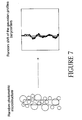
- Figure 6 illustrates the effect of microscopic reflectance irregularities (as imaged on a viewing slit) on the spectrophotometric profile and the corresponding measurement errors as registered by an imaging array in a spectrograph;
- Figure 7 illustrates the random shift of the gaussian profiles (light intensity profiles) caused by surface irregularities in the measured.object;
- Figure 8 is a diagram showing a surface microstructure compensation technique incorporated into the viewing subsystem of the optoelectronic device in the present invention; and
- Figure 9 illustrates the reconstruction of the real spectral composition from a slit image captured directly from the light intensities on the viewing slit of a spectrograph.
-
- The following description of the present invention is merely exemplary in nature and is in no way intended to limit the invention or its uses. Moreover, the following description, while depicting an optoelectronic system using spatiochromatic triangulation for determining a three-dimensional topography of an object, is intended to adequately teach one skilled in the art to make and use an optoelectronic system for a variety of measurement applications using in depth chromatic coding of an object surface.
- An
optoelectronic system 10, including anilluminating subsystem 12 for illuminating anobject 16 across acutting plane 32 and aviewing subsystem 14 for collecting the light reflected by theobject 16 and for generating a three-dimensional topography of theobject 16, is illustrated in Figure 1. In this first embodiment of the present invention, the components ofoptoelectronic system 10 are shown in an "in plane" configuration. -
Illuminating subsystem 12 comprises apolychromatic light source 20 that illuminates a continuous spectrum throughrelay optics 22 which focus the source onto afirst slit 24 oriented along the y-axis.Polychromatic light source 20 may be an incandescent light source, an Arc lamp (i.e., Xenon Arc) having a continuous spectrum and functioning in either a continuous or a flash mode, or other light sources optically coupled together in order to provide a large spectral bandwidth (i.e., superradiant diodes or light emitting diodes LEDs).Light source 20 may also be located remotely fromilluminating subsystem 12 and delivered through a fiber optic medium or other medium to illuminatingsubsystem 12. - The image from
source slit 24 passes through a dispersingelement 26 prior to illuminating ameasuring space 30. Dispersingelement 26 may comprise a prism, concave diffraction grating, diffraction lens, or other dispersing optics that function to illuminate a three-dimensional measuring space 30 with a continuum of monochromatic images oriented in the y-dimension.Cutting plane 32 is a measuring plane defined by the x-axis and z-axis of a coordinate system located in measuringspace 30. Dispersingelement 26 may also focus these images at nominal focus points in measuringspace 30. - Generic wavelengths from λ1 to λn are shown extending across
cutting plane 32 in Figure 2, and thus providing in depth chromatic coding of the surface of a measured object. The wavelength range of the light beams corresponds to the spread of impinging polychromatic light beam being delivered bylight source 20. - Referring to Figure 1, for the "in plane" configuration a pinhole may be used in place of
slit 24 , resulting in a continuum of monochromatic point images together forming a plane in measuringspace 30. This approach illuminates only that part of theobject 16 visible to theviewing subsystem 14, placing higher tolerances on mutual alignment ofilluminating subsystem 12 and viewingsubsystem 16, while reducing optical power required oflight source 20 and reducing possible interference effects from light not directly viewed by 16. -
Object 16 to be measured may be partially or completely located inside measuringspace 30. To displacecutting plane 32 along the surface ofobject 16, the object in the preferred embodiment is firmly fastened to a motorizedmechanical means 34.Mechanical means 34 then operates to translateobject 16 along the y-axis and/or to rotateobject 16 about any given axis in order to acquire successively all of the views of the surface ofobject 16 necessary to complete its examination/representation. Those skilled in the art will appreciate that mechanical means may include a variety of drive assemblies and motors, for example, the ATS100 series manufactured by Aerotech, Inc. of Pittsburgh, Pennsylvania. An encoder/control module 36 is also coupled tomechanical means 34 for electronically driving and synchronizingmechanical means 34. -
Viewing subsystem 14 comprises animaging spectrograph 40 having a viewing slit 42 in parallel alignment with the x-axis of measuringspace 30. The image plane ofspectrograph 40 aligns with an image created by the intersection of cuttingplane 32 and the measuring surface ofobject 16. Arelay lens 50 having a large depth of field serves to demagnify this image onto viewing slit 42 ofspectrograph 40. Internal to spectrograph 40, a dispersingelement 44 projects this image onto agrayscale imaging array 46 which is located in the image plane ofspectrograph 40. To improve resolution,imaging array 46 should map the height of its array to the full spectrum of wavelengths used in the system. A charge coupled device (CCD) or other similar device known in the art may be employed as theimaging array 46. Animage data processor 48, such as a digital signal processor or a general purpose computer, is coupled tospectrograph 40 for recording, processing and visualizing measurements ofobject 16 as registered byimaging array 46. -
Imaging optics 50 may be positioned inside and/or outside ofspectrograph 40. Since telecentric optics are not practical for imaging large measuring spaces (e.g., high quality lens > 1 inch (= 25,6 mm) in size are expensive to manufacture),viewing subsystem 14 may be configured without telecentric optics. Classic relay lens or other non-telecentric optics may replace telecentric optics in the present invention provided a complementary pupil transport is added in front of viewing slit 42. Since telecentric optics are used to ensure a constant magnification over the entire depth of field, a software implemented correction is preferably used in conjunction with non-telecentric optics. - In operation, measured
object 16 is placed into measuringspace 30 which is illuminated with a continuum of monochromatic images fromlight source 20 that has passed through dispersingelement 26. As a result, an in depth chromatic coding of the surface of measuringobject 16 occurs and the wavelength of the light reflected by measuredobject 16 will translate into an z-axis measurement. In other words, a color coded (x,λ) representation of cutting plane (x,z) is imaged ontoslit 42 ofspectrograph 40 and then registered bygrayscale imaging array 46. Due to perspective and optical distortion, the image is only representative of the surface of the measuredobject 16. However, through the use of a mathematical mapping generated during a calibration process ofoptoelectronic system 10,image processor 48 can reconstruct a digitized contour line equivalent to the surface ofobject 16 along cuttingplane 32. For a given contour line the signal onimaging array 46 appears as a curved line with a transverse gaussian profile whose position alongimaging array 46 depends on the spectral content of the corresponding point on the surface ofobject 16. Various signal processing techniques may be employed byimage processor 48 to determine the barycenter of the gaussian profile and thus determine a corresponding z measurement. - Although some applications of
optoelectronic system 10 may only utilize a single contour line from the surface of an object, other applications will need a digitized reconstruction of its entire surface area. As best seen in Figure 3, since only one cuttingplane 70 aligns with theimage plane 72 of spectrograph (not shown), additional measurements along successive parallel cutting planes will be needed to reconstruct the surface ofobject 16. Therefore, in order to measure the entire surface area, mechanical means 34 must translate object 16 (along the y-axis) with respect to the image plane of a fixed spectrograph. In an alternate approach to measuring this surface area, measuredobject 16 may be fastened to an immovable holding member so that viewingsubsystem 14 is translated (along the y-axis) with respect to fixedobject 16. In either case, spectrophotometric analysis of each successive cutting plane image leads to the three dimensional topography ofobject 16. - In the first embodiment of the present invention,
optoelectronic system 10 is referred to as an "in plane" configuration. In this "in plane" configuration, referring back to Figure 2, the resolution of the left side of measuringspace 30 is limited to the wavelengths from λ1 to λi, and similarly the right side of measuringspace 30 is limited to the wavelengths from λj to λn. To improve resolution in the present invention, a broad range of wavelengths should correlate to z measurements along the x-axis. Although increasing the triangulation angle will increase the resolution for this z-axis measurement, it also contributes to an occlusion problem caused by the object relief obstructing the illuminating image. - A second preferred embodiment, in Figure 4, utilizes a "v-shape" configuration to reduce the triangulation angle in the
optoelectronic system 100 of the present invention. In this preferred embodiment, a source slit 101 and viewing slit 103 are both in parallel alignment with the y-axis of measuringspace 30. By turning theviewing subsystem triangulation angle 110 can be significantly reduced without loosing the full advantage of the entire spectrum of wavelengths from λ1 to λn.Optoelectronic system 100 can otherwise include all of the basic system components (or variations) as discussed in Figure 1. - For the "v-shape" configuration correction for perspective distortions can be made by orienting the
grayscale imaging array 46 in such a manner as to have the wavelength oriented along the columns and the x-axis oriented along the rows. If telecentric optics were used, the measured position of z is a function of row number R and the measured points along the x-axis are approximately a linear function of the column number C. That is,
x and z = measured points in the field-of-view
R and C = row and column of a point in image array - These equations are only strictly true for telecentric optics. For an embodiment of the present invention using non-telecentric imaging optics, perspective distortions must be compensated for by adding some x-dependence into the calculation of fz, as well as adding some z-dependence into the calculation of fx. Therefore, the general modelling of this problem is represented by:
- Polynomials of the above form can solve the perspective problem in a non-telecentric system. Positioning a calibration target in front of a sensor at n positions will provide samples of Z1...Zn, Y1...Yn, R1...Rn and C1...Cn, and thus provide sufficient information to provide a least-squares solution to identify the ai and bi coefficients. Additional nonlinear components, such as aiRjCk and/or biRjCk, may be added to the above equation to compensate for other optical/geometric distortions. Accordingly, as will readily be recognized by those skilled in the art, a software-implemented correction modelled from the above equations can be used to resolve the perspective problem in the absence of telescopic optics in the present invention. A similar process may be implemented to correct for distortions in the "in-plane" configuration.
-
Optoelectronic system 100 of the preferred embodiment has been realized in a 267mm × 172mm × 68mm sensor weighing 3 kg. The sensor uses a 50W Tungsten Halogen lamp as its light source and a ½ " hyper HAD type CCD from Sony having 646 (spectral direction)*484 pixel resolution. The viewing slit is 20 micrometers wide and 5 millimeters high and is made of a chromium plated thin glass plate (1.5mm × 15mm). The slit is imaged through the spectrograph onto the CCD by a telecentric combination of two achromatic doublets (73mm focal length and 17mm in diameter). The mean dispersion is 0.62 nanometer per pixel on the CCD thus allowing 400 nanometers spectral range (comprised between 500 and 900 nanometers) to be imaged on the CCD. Using a "v-shape" configuration,optoelectronic system 100 achieves spatial resolution of 100*130 µm for x,y and less than 10 µm for z measurements. - In an imaging spectrograph, the entrance slit width is assumed to be homogeneously illuminated, and when illuminated by a light source having a small spectral width (Δλ) its image on a monochromatic imaging array will have a gaussian profile as seen in Figure 5. Unlike monochromatic triangulation methods, the performance of an optoelectronic system based on spatiochromatic triangulation is affected by the width of the spectrograph slit and the surface imperfections on the measured surface. If the slit is too narrow, the signal passed is too low; whereas if the slit is made wider, more light passes through the slit, but the image becomes increasingly "lumpy". The light reflected from the target surface includes "lumpy" distortions caused by surface imperfection in the measured object. To illustrate this problem, consider a flat target, with a checkerboard pattern as shown in Figure 6, as viewed by a spectrograph. The location of the mean (barycenter) of the light distribution within the slit varies along the slit, and thus leads to misinterpretation of the signal when imaged through the spectrograph. The top profile from Figure 6 is centered as the light is distributed evenly on the slit; whereas the bottom three profiles each exhibit asymmetrical offsets due to a variation in the light intensity imaged at the slit. The position of the light requires centering in the slit for an accurate mapping of the light onto the spectrograph, otherwise these offset variations will be translated into measurement errors. Similarly, measuring a surface with microscopic reflectance irregularities will create measurement errors when digitizing the topography of an object. For example, in the "v-plane" configuration of the presents invention, a flat target surface should result in an image with the same wavelength (i.e., same color). However, the presence of surface imperfections can cause an apparent red shift or blue shift in the imaged signal which is incorrectly interpreted as depth variations in the flat target surface.
- The optoelectronic system according to the present invention preferably uses a surface microstructure compensation technique to overcome this problem. In particular, as shown in Figure 8, the optoelectronic system of the present invention further includes a set of beam splitters interposed into the image plane of a
spectrograph 122. Afirst spliner 126 is located between aviewing slit 124 ofspectrograph 122 and dispersingelements 130; whereas asecond splitter 128 is positioned between dispersingelements 130 and amonochromatic imaging array 132.First splitter 126 andsecond splitter 128 are used to generate aslit image 140 directly from the light intensities onviewing slit 124. By allocating part ofimaging array 132 toslit image 140, one single imaging array can be used for profiling slitimage 140 and theimage 142 passed throughspectrograph 122.Relay lens 134 may also be incorporated intoviewing subsystem 120. - Referring to Figure 7, a random spectrophotometric microstructure from the measured surface results in a random shift of gaussian profiles as registered by the imaging array of a spectrograph. In Figure 9, measurements of the light intensity from viewing
slit 124 as captured inslit image 140 are then used to reconstruct the actual spectral composition of each point alongviewing slit 124. As will be apparent to one skilled in the art, animage processor 150 may be used to read the centers of light intensities fromslit image 140 and then to use this information to remove the apparent red and blue shifts that occur inspectrograph image 142. As a result of this surface microstructure compensation technique,image processor 150 can produce a correctedimage 144. In an alternative approach, a second imaging array (not shown) may be placed before thesecond splitter 128 for registering splitimage 140. - A method for surface digitization of an object using spatiochromatic triangulation will now be described. First, a polychromatic light source, that may also pass through a relay lens, is imaged onto a source slit. Next, the slit image passes through a dispersing element, and thus providing in depth chromatic coding of the object by illuminating a measuring space (containing the object) with a continuum of monochromatic images. The image plane of an imaging spectrograph aligns with the surface of the object and an imaging array located in the image plane registers an image of the object. Finally, an image processor generates a digitized contour line from the object.
- The foregoing discloses and describes merely exemplary embodiments of the present invention. One skilled in the art will readily recognize from such discussion, and from the accompanying drawings and claims, that various changes, modifications and variations can be made therein without departing from the scope of the present invention as defined in the claims.
Claims (13)
- An optoelectronic device for the digitization of an object using spatiochromatic triangulation, said device comprising:a polychromatic light source (20);relay optics (22) positioned in an illuminating plane of said light source (20) for imaging said light source onto a source slit or pinhole (24, 101);a dispersing element (26, 102) in the form of a prism (102) or a concave diffraction grating (26) for illuminating a measuring space (30) with a continuum of monochromatic images along a measuring cutting plane (32) providing in depth chromatic coding of said object (16), wherein said object (16) is located in said measuring space (30);an imaging spectrograph (40) having a viewing slit (42, 103) whose image plane aligns with an image generated by the intersection of said cutting plane (32) and the surface of said object (16); andan imaging array (46) located in said image plane of said spectrograph for registering said image.
- The optoelectronic system of claim 1, wherein said source slit or pinhole (24, 101) is further defined as a pinhole for forming point images.
- The optoelectronic system of claim 1 or 2, further comprising a telecentric relay lens (50) for projecting said image onto said viewing slit (42, 103).
- The optoelectronic system of claim 1 or 2, further comprising a relay lens (50) for projecting said image onto said viewing slit (42) and an image processor for correcting perspective distortion.
- The optoelectronic system of any of claims 1 to 3, further comprising an image processor (48) coupled to said imaging array (46) for processing said registered image using spectrophotometric analysis and generating a digitized contour line from said object (16).
- The optoelectronic system of any of claims 1 to 5, further comprising a mechanical means (34) for translating said object (16) within said measuring space (30) and an electronic controller (36) for driving and synchronizing said mechanical means (34), wherein said object (16) is fastened to said mechanical means (34) and by translating said object (16), a plurality of images are registered along successive parallel cutting planes to reconstruct a topography of said object (16).
- The optoelectronic system of any of claims 1 to 6, wherein the imaging spectrograph (40) further includes a further dispersing element (44) for projecting said image onto an imaging array (46).
- The optoelectronic system cf claim 7, further including a first beam splitter (126) interposed between said viewing slit (42, 103, 124) and said further dispersing element (44) for generating a direct slit image (144), wherein said imaging array (46) views both, a dispersed image (142) having passed through said further dispersing element (44) and said direct slit image (144), whereby said direct slit image (144) is used to compensate for apparent wavelength shifts in said dispersed image (142).
- The optoelectronic system of any of claims 1 to 8, wherein said image array (46) is a greyscale imaging array (46).
- A method for surface digitization of an object (16) using spatiochromatic triangulation, comprising steps of:imaging a light source (20) onto a source slit or pinhole (24, 101);illuminating a measuring space (30) with a continuum of monochromatic images along a cutting plane (32) by passing said slit or pinhole image through a dispersing element (26, 102), thus providing in depth chromatic coding of said object (16), where said object is located in said measuring space (30);imaging an image of said object on a spectrograph (44) through a viewing slit (42, 103) whose image plane aligns with an image generated by the intersection of said cutting plane (32) and the surface of said object (16); andregistering said image on an imaging array (46) located in the image plane of said spectrograph (44).
- The method of claim 10, further comprising the step of generating a digitized contour line from said object (16) using spectrophotometric analysis.
- The method of claim 11, wherein an image processor (48) is coupled to said imaging array (46) for processing said image into a digitized contour line.
- The method of claim 10, further comprising the step of transiating said object (16) within the measuring space (30) using a mechanical means (34), whereby by translating said object (16), a plurality of images are registered along successive parallel cutting planes to reconstruct a topography of said object (16).
Applications Claiming Priority (1)
| Application Number | Priority Date | Filing Date | Title |
|---|---|---|---|
| PCT/IB1997/001406 WO1999024786A1 (en) | 1997-11-06 | 1997-11-06 | Optoelectronic system using spatiochromatic triangulation |
Publications (2)
| Publication Number | Publication Date |
|---|---|
| EP0950168A1 EP0950168A1 (en) | 1999-10-20 |
| EP0950168B1 true EP0950168B1 (en) | 2005-08-17 |
Family
ID=11004628
Family Applications (1)
| Application Number | Title | Priority Date | Filing Date |
|---|---|---|---|
| EP97910573A Expired - Lifetime EP0950168B1 (en) | 1997-11-06 | 1997-11-06 | Optoelectronic system using spatiochromatic triangulation |
Country Status (9)
| Country | Link |
|---|---|
| US (1) | US6573998B2 (en) |
| EP (1) | EP0950168B1 (en) |
| JP (1) | JP2001507808A (en) |
| AT (1) | ATE302401T1 (en) |
| AU (1) | AU4791397A (en) |
| CA (1) | CA2278332C (en) |
| DE (1) | DE69734010T2 (en) |
| IL (1) | IL130780A (en) |
| WO (1) | WO1999024786A1 (en) |
Cited By (3)
| Publication number | Priority date | Publication date | Assignee | Title |
|---|---|---|---|---|
| WO2013174826A1 (en) | 2012-05-21 | 2013-11-28 | Sysmelec Sa | Chromatic converter for altimetry |
| WO2023046770A1 (en) * | 2021-09-22 | 2023-03-30 | WICKON HIGHTECH GmbH | Inspection system and method for analyzing faults |
| WO2023046769A1 (en) * | 2021-09-22 | 2023-03-30 | WICKON HIGHTECH GmbH | Inspection system and method for analyzing faults |
Families Citing this family (87)
| Publication number | Priority date | Publication date | Assignee | Title |
|---|---|---|---|---|
| US11026768B2 (en) | 1998-10-08 | 2021-06-08 | Align Technology, Inc. | Dental appliance reinforcement |
| KR100729290B1 (en) * | 2000-01-07 | 2007-06-25 | 사이버옵틱스 코포레이션 | Phase profilometry system with telecentric projector |
| US6549647B1 (en) | 2000-01-07 | 2003-04-15 | Cyberoptics Corporation | Inspection system with vibration resistant video capture |
| US6593705B1 (en) | 2000-01-07 | 2003-07-15 | Cyberoptics Corporation | Rapid-firing flashlamp discharge circuit |
| CA2301822A1 (en) | 2000-03-24 | 2001-09-24 | 9071 9410 Quebec Inc. | Simultaneous projection of several patterns with simultaneous acquisition for inspection of objects in three-dimensions |
| CA2306515A1 (en) * | 2000-04-25 | 2001-10-25 | Inspeck Inc. | Internet stereo vision, 3d digitizing, and motion capture camera |
| DE10324934A1 (en) * | 2003-06-03 | 2004-12-23 | Carl Zeiss Jena Gmbh | Arrangement and a method for recognizing layers that are arranged on surfaces of components and determining their properties |
| US9492245B2 (en) | 2004-02-27 | 2016-11-15 | Align Technology, Inc. | Method and system for providing dynamic orthodontic assessment and treatment profiles |
| FI20040315A (en) * | 2004-02-27 | 2005-08-28 | Tameye Ky | Material error detection using a spectrum camera |
| JP2007101399A (en) * | 2005-10-05 | 2007-04-19 | Nikon Corp | Height measuring apparatus and method |
| US7878805B2 (en) | 2007-05-25 | 2011-02-01 | Align Technology, Inc. | Tabbed dental appliance |
| DE102007044530B4 (en) * | 2007-09-18 | 2009-06-10 | VMA Gesellschaft für visuelle Meßtechnik und Automatisierung mbH | Arrangement for measuring the thickness and the distance of transparent objects |
| US8738394B2 (en) | 2007-11-08 | 2014-05-27 | Eric E. Kuo | Clinical data file |
| JP2011509812A (en) | 2008-01-23 | 2011-03-31 | センサブル テクノロジーズ インコーポレイテッド | Tactile controllable dental modeling system |
| US8059280B2 (en) | 2008-01-31 | 2011-11-15 | Cyberoptics Corporation | Method for three-dimensional imaging using multi-phase structured light |
| US8108189B2 (en) | 2008-03-25 | 2012-01-31 | Align Technologies, Inc. | Reconstruction of non-visible part of tooth |
| US9492243B2 (en) | 2008-05-23 | 2016-11-15 | Align Technology, Inc. | Dental implant positioning |
| US8092215B2 (en) | 2008-05-23 | 2012-01-10 | Align Technology, Inc. | Smile designer |
| US8172569B2 (en) | 2008-06-12 | 2012-05-08 | Align Technology, Inc. | Dental appliance |
| US8152518B2 (en) | 2008-10-08 | 2012-04-10 | Align Technology, Inc. | Dental positioning appliance having metallic portion |
| US8292617B2 (en) | 2009-03-19 | 2012-10-23 | Align Technology, Inc. | Dental wire attachment |
| US8765031B2 (en) | 2009-08-13 | 2014-07-01 | Align Technology, Inc. | Method of forming a dental appliance |
| US8134719B2 (en) * | 2010-03-19 | 2012-03-13 | Carestream Health, Inc. | 3-D imaging using telecentric defocus |
| FR2958298B1 (en) * | 2010-04-06 | 2014-10-17 | Commissariat Energie Atomique | METHOD FOR DETECTING AMAS FROM BIOLOGICAL PARTICLES |
| US9241774B2 (en) | 2010-04-30 | 2016-01-26 | Align Technology, Inc. | Patterned dental positioning appliance |
| US9211166B2 (en) | 2010-04-30 | 2015-12-15 | Align Technology, Inc. | Individualized orthodontic treatment index |
| US9403238B2 (en) | 2011-09-21 | 2016-08-02 | Align Technology, Inc. | Laser cutting |
| DE102011117523B3 (en) * | 2011-11-03 | 2013-04-18 | Fraunhofer-Gesellschaft zur Förderung der angewandten Forschung e.V. | Device for optically determining the surface geometry of a three-dimensional sample |
| US9375300B2 (en) | 2012-02-02 | 2016-06-28 | Align Technology, Inc. | Identifying forces on a tooth |
| US9220580B2 (en) | 2012-03-01 | 2015-12-29 | Align Technology, Inc. | Determining a dental treatment difficulty |
| US9414897B2 (en) | 2012-05-22 | 2016-08-16 | Align Technology, Inc. | Adjustment of tooth position in a virtual dental model |
| US9947813B2 (en) | 2012-07-27 | 2018-04-17 | Zfx Gmbh | System and method for illuminating a sample and collecting light reflected from the sample |
| FI125408B (en) * | 2012-09-17 | 2015-09-30 | Focalspec Oy | Method and gauge for measuring surface distance, target thickness and optical properties |
| US10126252B2 (en) | 2013-04-29 | 2018-11-13 | Cyberoptics Corporation | Enhanced illumination control for three-dimensional imaging |
| US9261358B2 (en) | 2014-07-03 | 2016-02-16 | Align Technology, Inc. | Chromatic confocal system |
| US9439568B2 (en) | 2014-07-03 | 2016-09-13 | Align Technology, Inc. | Apparatus and method for measuring surface topography optically |
| US9261356B2 (en) | 2014-07-03 | 2016-02-16 | Align Technology, Inc. | Confocal surface topography measurement with fixed focal positions |
| US10772506B2 (en) | 2014-07-07 | 2020-09-15 | Align Technology, Inc. | Apparatus for dental confocal imaging |
| US11006828B2 (en) | 2014-07-17 | 2021-05-18 | 1 Sonic Medical Corporation, S.A.S. | Measurement of ocular parameters using vibrations induced in the eye |
| US9693839B2 (en) | 2014-07-17 | 2017-07-04 | Align Technology, Inc. | Probe head and apparatus for intraoral confocal imaging using polarization-retarding coatings |
| US9675430B2 (en) | 2014-08-15 | 2017-06-13 | Align Technology, Inc. | Confocal imaging apparatus with curved focal surface |
| US9660418B2 (en) | 2014-08-27 | 2017-05-23 | Align Technology, Inc. | VCSEL based low coherence emitter for confocal 3D scanner |
| US9610141B2 (en) | 2014-09-19 | 2017-04-04 | Align Technology, Inc. | Arch expanding appliance |
| US10449016B2 (en) | 2014-09-19 | 2019-10-22 | Align Technology, Inc. | Arch adjustment appliance |
| US9744001B2 (en) | 2014-11-13 | 2017-08-29 | Align Technology, Inc. | Dental appliance with cavity for an unerupted or erupting tooth |
| US10504386B2 (en) | 2015-01-27 | 2019-12-10 | Align Technology, Inc. | Training method and system for oral-cavity-imaging-and-modeling equipment |
| US10248883B2 (en) | 2015-08-20 | 2019-04-02 | Align Technology, Inc. | Photograph-based assessment of dental treatments and procedures |
| FI127908B (en) * | 2015-09-22 | 2019-05-15 | Teknologian Tutkimuskeskus Vtt Oy | Method and apparatus for measuring the height of a surface |
| US11931222B2 (en) | 2015-11-12 | 2024-03-19 | Align Technology, Inc. | Dental attachment formation structures |
| US11554000B2 (en) | 2015-11-12 | 2023-01-17 | Align Technology, Inc. | Dental attachment formation structure |
| US11596502B2 (en) | 2015-12-09 | 2023-03-07 | Align Technology, Inc. | Dental attachment placement structure |
| US11103330B2 (en) | 2015-12-09 | 2021-08-31 | Align Technology, Inc. | Dental attachment placement structure |
| WO2017218947A1 (en) | 2016-06-17 | 2017-12-21 | Align Technology, Inc. | Intraoral appliances with sensing |
| US10383705B2 (en) | 2016-06-17 | 2019-08-20 | Align Technology, Inc. | Orthodontic appliance performance monitor |
| US10507087B2 (en) | 2016-07-27 | 2019-12-17 | Align Technology, Inc. | Methods and apparatuses for forming a three-dimensional volumetric model of a subject's teeth |
| DK3578131T3 (en) | 2016-07-27 | 2020-12-21 | Align Technology Inc | Intraoral scanner with dental diagnostic features |
| WO2018085718A2 (en) | 2016-11-04 | 2018-05-11 | Align Technology, Inc. | Methods and apparatuses for dental images |
| AU2017366755B2 (en) | 2016-12-02 | 2022-07-28 | Align Technology, Inc. | Methods and apparatuses for customizing rapid palatal expanders using digital models |
| WO2018102702A1 (en) | 2016-12-02 | 2018-06-07 | Align Technology, Inc. | Dental appliance features for speech enhancement |
| WO2018102770A1 (en) | 2016-12-02 | 2018-06-07 | Align Technology, Inc. | Force control, stop mechanism, regulating structure of removable arch adjustment appliance |
| CN110035708B (en) | 2016-12-02 | 2021-11-05 | 阿莱恩技术有限公司 | Palatal expander and method of expanding a palate |
| US10548700B2 (en) | 2016-12-16 | 2020-02-04 | Align Technology, Inc. | Dental appliance etch template |
| US10456043B2 (en) | 2017-01-12 | 2019-10-29 | Align Technology, Inc. | Compact confocal dental scanning apparatus |
| US10779718B2 (en) | 2017-02-13 | 2020-09-22 | Align Technology, Inc. | Cheek retractor and mobile device holder |
| US10613515B2 (en) | 2017-03-31 | 2020-04-07 | Align Technology, Inc. | Orthodontic appliances including at least partially un-erupted teeth and method of forming them |
| US11045283B2 (en) | 2017-06-09 | 2021-06-29 | Align Technology, Inc. | Palatal expander with skeletal anchorage devices |
| WO2019005808A1 (en) | 2017-06-26 | 2019-01-03 | Align Technology, Inc. | Biosensor performance indicator for intraoral appliances |
| US10885521B2 (en) | 2017-07-17 | 2021-01-05 | Align Technology, Inc. | Method and apparatuses for interactive ordering of dental aligners |
| CN111107806B (en) | 2017-07-21 | 2022-04-19 | 阿莱恩技术有限公司 | Jaw profile anchoring |
| WO2019023461A1 (en) | 2017-07-27 | 2019-01-31 | Align Technology, Inc. | Tooth shading, transparency and glazing |
| EP4278957A3 (en) | 2017-07-27 | 2024-01-24 | Align Technology, Inc. | System and methods for processing an orthodontic aligner by means of an optical coherence tomography |
| WO2019035979A1 (en) | 2017-08-15 | 2019-02-21 | Align Technology, Inc. | Buccal corridor assessment and computation |
| WO2019036677A1 (en) | 2017-08-17 | 2019-02-21 | Align Technology, Inc. | Dental appliance compliance monitoring |
| US10813720B2 (en) | 2017-10-05 | 2020-10-27 | Align Technology, Inc. | Interproximal reduction templates |
| EP3700458B1 (en) | 2017-10-27 | 2023-06-07 | Align Technology, Inc. | Alternative bite adjustment structures |
| CN111295153B (en) | 2017-10-31 | 2023-06-16 | 阿莱恩技术有限公司 | Dental appliance with selective bite loading and controlled tip staggering |
| EP3703607A2 (en) | 2017-11-01 | 2020-09-09 | Align Technology, Inc. | Automatic treatment planning |
| WO2019100022A1 (en) | 2017-11-17 | 2019-05-23 | Align Technology, Inc. | Orthodontic retainers |
| EP3716885B1 (en) | 2017-11-30 | 2023-08-30 | Align Technology, Inc. | Orthodontic intraoral appliances comprising sensors |
| WO2019118876A1 (en) | 2017-12-15 | 2019-06-20 | Align Technology, Inc. | Closed loop adaptive orthodontic treatment methods and apparatuses |
| US10980613B2 (en) | 2017-12-29 | 2021-04-20 | Align Technology, Inc. | Augmented reality enhancements for dental practitioners |
| AU2019212649A1 (en) | 2018-01-26 | 2020-07-02 | Align Technology, Inc. | Diagnostic intraoral scanning and tracking |
| US11937991B2 (en) | 2018-03-27 | 2024-03-26 | Align Technology, Inc. | Dental attachment placement structure |
| CN116211501A (en) | 2018-04-11 | 2023-06-06 | 阿莱恩技术有限公司 | Palate expander, palate expander device and system, and method for forming palate expander |
| JP7410969B2 (en) | 2020-06-11 | 2024-01-10 | 東莞市神州視覚科技有限公司 | Spectral confocal measurement device and measurement method |
| DE102021124507A1 (en) | 2021-09-22 | 2023-03-23 | WICKON HIGHTECH GmbH | Inspection system and procedures for failure analysis |
| CN114111626B (en) * | 2021-11-26 | 2023-08-22 | 深圳技术大学 | Light field camera three-dimensional measurement device and system based on coaxial projection |
Citations (1)
| Publication number | Priority date | Publication date | Assignee | Title |
|---|---|---|---|---|
| EP0890822A2 (en) * | 1997-07-09 | 1999-01-13 | YEDA RESEARCH AND DEVELOPMENT Co. LTD. | A triangulation method and system for color-coded optical profilometry |
Family Cites Families (3)
| Publication number | Priority date | Publication date | Assignee | Title |
|---|---|---|---|---|
| CA1316590C (en) * | 1989-04-17 | 1993-04-20 | Marc Rioux | Three-dimensional imaging device |
| JPH07128027A (en) * | 1993-11-02 | 1995-05-19 | Toshiba Corp | Solder-paste inspection device |
| US5785651A (en) * | 1995-06-07 | 1998-07-28 | Keravision, Inc. | Distance measuring confocal microscope |
-
1997
- 1997-06-11 US US09/341,197 patent/US6573998B2/en not_active Expired - Fee Related
- 1997-11-06 CA CA002278332A patent/CA2278332C/en not_active Expired - Lifetime
- 1997-11-06 EP EP97910573A patent/EP0950168B1/en not_active Expired - Lifetime
- 1997-11-06 JP JP52576799A patent/JP2001507808A/en not_active Ceased
- 1997-11-06 DE DE69734010T patent/DE69734010T2/en not_active Expired - Lifetime
- 1997-11-06 WO PCT/IB1997/001406 patent/WO1999024786A1/en active IP Right Grant
- 1997-11-06 IL IL13078097A patent/IL130780A/en not_active IP Right Cessation
- 1997-11-06 AU AU47913/97A patent/AU4791397A/en not_active Abandoned
- 1997-11-06 AT AT97910573T patent/ATE302401T1/en not_active IP Right Cessation
Patent Citations (1)
| Publication number | Priority date | Publication date | Assignee | Title |
|---|---|---|---|---|
| EP0890822A2 (en) * | 1997-07-09 | 1999-01-13 | YEDA RESEARCH AND DEVELOPMENT Co. LTD. | A triangulation method and system for color-coded optical profilometry |
Cited By (4)
| Publication number | Priority date | Publication date | Assignee | Title |
|---|---|---|---|---|
| WO2013174826A1 (en) | 2012-05-21 | 2013-11-28 | Sysmelec Sa | Chromatic converter for altimetry |
| US9261352B2 (en) | 2012-05-21 | 2016-02-16 | Unitechnologies Sa | Chromatic converter for altimetry |
| WO2023046770A1 (en) * | 2021-09-22 | 2023-03-30 | WICKON HIGHTECH GmbH | Inspection system and method for analyzing faults |
| WO2023046769A1 (en) * | 2021-09-22 | 2023-03-30 | WICKON HIGHTECH GmbH | Inspection system and method for analyzing faults |
Also Published As
| Publication number | Publication date |
|---|---|
| JP2001507808A (en) | 2001-06-12 |
| US20020075484A1 (en) | 2002-06-20 |
| CA2278332C (en) | 2009-01-27 |
| DE69734010T2 (en) | 2006-06-14 |
| CA2278332A1 (en) | 1999-05-20 |
| IL130780A (en) | 2003-04-10 |
| ATE302401T1 (en) | 2005-09-15 |
| WO1999024786A1 (en) | 1999-05-20 |
| AU4791397A (en) | 1999-05-31 |
| DE69734010D1 (en) | 2005-09-22 |
| US6573998B2 (en) | 2003-06-03 |
| IL130780A0 (en) | 2001-01-28 |
| EP0950168A1 (en) | 1999-10-20 |
Similar Documents
| Publication | Publication Date | Title |
|---|---|---|
| EP0950168B1 (en) | Optoelectronic system using spatiochromatic triangulation | |
| US6538751B2 (en) | Image capturing apparatus and distance measuring method | |
| US6268923B1 (en) | Optical method and system for measuring three-dimensional surface topography of an object having a surface contour | |
| US7532333B2 (en) | Method and apparatus for determining the shape and the local surface normals of specular surfaces | |
| US6611344B1 (en) | Apparatus and method to measure three dimensional data | |
| USRE46012E1 (en) | Non-contact probe | |
| US5546189A (en) | Triangulation-based 3D imaging and processing method and system | |
| US6714308B2 (en) | Rapid in-situ mastering of an aspheric fizeau | |
| US5085502A (en) | Method and apparatus for digital morie profilometry calibrated for accurate conversion of phase information into distance measurements in a plurality of directions | |
| KR100815283B1 (en) | System for simultaneous projections of multiple phase-shifted patterns for the three-dimensional inspection of an object | |
| US6549288B1 (en) | Structured-light, triangulation-based three-dimensional digitizer | |
| US6771375B2 (en) | Apparatus and method for measuring aspherical optical surfaces and wavefronts | |
| US20080117438A1 (en) | System and method for object inspection using relief determination | |
| JPH0792372B2 (en) | Method for measuring an optical surface feature of a mirror and apparatus for determining the feature | |
| CA2334225C (en) | Method and device for opto-electrical acquisition of shapes by axial illumination | |
| TW202011124A (en) | Chromatic confocal area sensor | |
| EP0985133B1 (en) | Apparatus for position determination | |
| CN111406197A (en) | Transparent or translucent material curved surface contour detection system | |
| JP2533514B2 (en) | Depth / thickness measuring device | |
| CA2607822C (en) | Optoelectronic system using spatiochromatic triangulation | |
| US20050226533A1 (en) | Method for measuring the location of an object by phase detection | |
| KR100641885B1 (en) | light phase interferrometry method and system for horizontal scanning type | |
| EP1139090A2 (en) | Leaded integrated circuit inspection system | |
| KR20000069937A (en) | Optoelectronic system using spatiochromatic triangulation | |
| CN110296666B (en) | Three-dimensional measuring device |
Legal Events
| Date | Code | Title | Description |
|---|---|---|---|
| PUAI | Public reference made under article 153(3) epc to a published international application that has entered the european phase |
Free format text: ORIGINAL CODE: 0009012 |
|
| 17P | Request for examination filed |
Effective date: 19990720 |
|
| AK | Designated contracting states |
Kind code of ref document: A1 Designated state(s): AT BE CH DE DK ES FI FR GB GR IE IT LI LU MC NL PT SE |
|
| 17Q | First examination report despatched |
Effective date: 20040121 |
|
| GRAP | Despatch of communication of intention to grant a patent |
Free format text: ORIGINAL CODE: EPIDOSNIGR1 |
|
| GRAS | Grant fee paid |
Free format text: ORIGINAL CODE: EPIDOSNIGR3 |
|
| GRAA | (expected) grant |
Free format text: ORIGINAL CODE: 0009210 |
|
| AK | Designated contracting states |
Kind code of ref document: B1 Designated state(s): AT BE CH DE DK ES FI FR GB GR IE IT LI LU MC NL PT SE |
|
| PG25 | Lapsed in a contracting state [announced via postgrant information from national office to epo] |
Ref country code: NL Free format text: LAPSE BECAUSE OF FAILURE TO SUBMIT A TRANSLATION OF THE DESCRIPTION OR TO PAY THE FEE WITHIN THE PRESCRIBED TIME-LIMIT Effective date: 20050817 Ref country code: LI Free format text: LAPSE BECAUSE OF FAILURE TO SUBMIT A TRANSLATION OF THE DESCRIPTION OR TO PAY THE FEE WITHIN THE PRESCRIBED TIME-LIMIT Effective date: 20050817 Ref country code: FI Free format text: LAPSE BECAUSE OF FAILURE TO SUBMIT A TRANSLATION OF THE DESCRIPTION OR TO PAY THE FEE WITHIN THE PRESCRIBED TIME-LIMIT Effective date: 20050817 Ref country code: CH Free format text: LAPSE BECAUSE OF FAILURE TO SUBMIT A TRANSLATION OF THE DESCRIPTION OR TO PAY THE FEE WITHIN THE PRESCRIBED TIME-LIMIT Effective date: 20050817 Ref country code: BE Free format text: LAPSE BECAUSE OF FAILURE TO SUBMIT A TRANSLATION OF THE DESCRIPTION OR TO PAY THE FEE WITHIN THE PRESCRIBED TIME-LIMIT Effective date: 20050817 Ref country code: AT Free format text: LAPSE BECAUSE OF FAILURE TO SUBMIT A TRANSLATION OF THE DESCRIPTION OR TO PAY THE FEE WITHIN THE PRESCRIBED TIME-LIMIT Effective date: 20050817 |
|
| REG | Reference to a national code |
Ref country code: GB Ref legal event code: FG4D |
|
| REG | Reference to a national code |
Ref country code: CH Ref legal event code: EP |
|
| REG | Reference to a national code |
Ref country code: IE Ref legal event code: FG4D |
|
| REF | Corresponds to: |
Ref document number: 69734010 Country of ref document: DE Date of ref document: 20050922 Kind code of ref document: P |
|
| PG25 | Lapsed in a contracting state [announced via postgrant information from national office to epo] |
Ref country code: IE Free format text: LAPSE BECAUSE OF NON-PAYMENT OF DUE FEES Effective date: 20051107 |
|
| PG25 | Lapsed in a contracting state [announced via postgrant information from national office to epo] |
Ref country code: SE Free format text: LAPSE BECAUSE OF FAILURE TO SUBMIT A TRANSLATION OF THE DESCRIPTION OR TO PAY THE FEE WITHIN THE PRESCRIBED TIME-LIMIT Effective date: 20051117 Ref country code: GR Free format text: LAPSE BECAUSE OF FAILURE TO SUBMIT A TRANSLATION OF THE DESCRIPTION OR TO PAY THE FEE WITHIN THE PRESCRIBED TIME-LIMIT Effective date: 20051117 Ref country code: DK Free format text: LAPSE BECAUSE OF FAILURE TO SUBMIT A TRANSLATION OF THE DESCRIPTION OR TO PAY THE FEE WITHIN THE PRESCRIBED TIME-LIMIT Effective date: 20051117 |
|
| PG25 | Lapsed in a contracting state [announced via postgrant information from national office to epo] |
Ref country code: ES Free format text: LAPSE BECAUSE OF FAILURE TO SUBMIT A TRANSLATION OF THE DESCRIPTION OR TO PAY THE FEE WITHIN THE PRESCRIBED TIME-LIMIT Effective date: 20051128 |
|
| PG25 | Lapsed in a contracting state [announced via postgrant information from national office to epo] |
Ref country code: MC Free format text: LAPSE BECAUSE OF NON-PAYMENT OF DUE FEES Effective date: 20051130 Ref country code: LU Free format text: LAPSE BECAUSE OF NON-PAYMENT OF DUE FEES Effective date: 20051130 |
|
| PG25 | Lapsed in a contracting state [announced via postgrant information from national office to epo] |
Ref country code: PT Free format text: LAPSE BECAUSE OF FAILURE TO SUBMIT A TRANSLATION OF THE DESCRIPTION OR TO PAY THE FEE WITHIN THE PRESCRIBED TIME-LIMIT Effective date: 20060117 |
|
| NLV1 | Nl: lapsed or annulled due to failure to fulfill the requirements of art. 29p and 29m of the patents act | ||
| REG | Reference to a national code |
Ref country code: CH Ref legal event code: PL |
|
| ET | Fr: translation filed | ||
| PLBE | No opposition filed within time limit |
Free format text: ORIGINAL CODE: 0009261 |
|
| STAA | Information on the status of an ep patent application or granted ep patent |
Free format text: STATUS: NO OPPOSITION FILED WITHIN TIME LIMIT |
|
| 26N | No opposition filed |
Effective date: 20060518 |
|
| REG | Reference to a national code |
Ref country code: IE Ref legal event code: MM4A |
|
| PGFP | Annual fee paid to national office [announced via postgrant information from national office to epo] |
Ref country code: GB Payment date: 20081204 Year of fee payment: 12 |
|
| PGFP | Annual fee paid to national office [announced via postgrant information from national office to epo] |
Ref country code: FR Payment date: 20081215 Year of fee payment: 12 |
|
| GBPC | Gb: european patent ceased through non-payment of renewal fee |
Effective date: 20091106 |
|
| REG | Reference to a national code |
Ref country code: FR Ref legal event code: ST Effective date: 20100730 |
|
| PG25 | Lapsed in a contracting state [announced via postgrant information from national office to epo] |
Ref country code: FR Free format text: LAPSE BECAUSE OF NON-PAYMENT OF DUE FEES Effective date: 20091130 |
|
| PG25 | Lapsed in a contracting state [announced via postgrant information from national office to epo] |
Ref country code: GB Free format text: LAPSE BECAUSE OF NON-PAYMENT OF DUE FEES Effective date: 20091106 |
|
| PGFP | Annual fee paid to national office [announced via postgrant information from national office to epo] |
Ref country code: IT Payment date: 20151127 Year of fee payment: 19 |
|
| PGFP | Annual fee paid to national office [announced via postgrant information from national office to epo] |
Ref country code: DE Payment date: 20170530 Year of fee payment: 20 |
|
| PG25 | Lapsed in a contracting state [announced via postgrant information from national office to epo] |
Ref country code: IT Free format text: LAPSE BECAUSE OF NON-PAYMENT OF DUE FEES Effective date: 20161106 |
|
| REG | Reference to a national code |
Ref country code: DE Ref legal event code: R071 Ref document number: 69734010 Country of ref document: DE |