EP0762143B1 - Chromatic optical ranging sensor - Google Patents
Chromatic optical ranging sensor Download PDFInfo
- Publication number
- EP0762143B1 EP0762143B1 EP96111721A EP96111721A EP0762143B1 EP 0762143 B1 EP0762143 B1 EP 0762143B1 EP 96111721 A EP96111721 A EP 96111721A EP 96111721 A EP96111721 A EP 96111721A EP 0762143 B1 EP0762143 B1 EP 0762143B1
- Authority
- EP
- European Patent Office
- Prior art keywords
- wavelength
- target
- sensor according
- reflected
- incident beam
- Prior art date
- Legal status (The legal status is an assumption and is not a legal conclusion. Google has not performed a legal analysis and makes no representation as to the accuracy of the status listed.)
- Expired - Lifetime
Links
Images


Classifications
-
- G—PHYSICS
- G01—MEASURING; TESTING
- G01S—RADIO DIRECTION-FINDING; RADIO NAVIGATION; DETERMINING DISTANCE OR VELOCITY BY USE OF RADIO WAVES; LOCATING OR PRESENCE-DETECTING BY USE OF THE REFLECTION OR RERADIATION OF RADIO WAVES; ANALOGOUS ARRANGEMENTS USING OTHER WAVES
- G01S17/00—Systems using the reflection or reradiation of electromagnetic waves other than radio waves, e.g. lidar systems
- G01S17/02—Systems using the reflection of electromagnetic waves other than radio waves
- G01S17/06—Systems determining position data of a target
- G01S17/08—Systems determining position data of a target for measuring distance only
-
- G—PHYSICS
- G01—MEASURING; TESTING
- G01S—RADIO DIRECTION-FINDING; RADIO NAVIGATION; DETERMINING DISTANCE OR VELOCITY BY USE OF RADIO WAVES; LOCATING OR PRESENCE-DETECTING BY USE OF THE REFLECTION OR RERADIATION OF RADIO WAVES; ANALOGOUS ARRANGEMENTS USING OTHER WAVES
- G01S17/00—Systems using the reflection or reradiation of electromagnetic waves other than radio waves, e.g. lidar systems
- G01S17/02—Systems using the reflection of electromagnetic waves other than radio waves
- G01S17/06—Systems determining position data of a target
- G01S17/46—Indirect determination of position data
-
- G—PHYSICS
- G01—MEASURING; TESTING
- G01S—RADIO DIRECTION-FINDING; RADIO NAVIGATION; DETERMINING DISTANCE OR VELOCITY BY USE OF RADIO WAVES; LOCATING OR PRESENCE-DETECTING BY USE OF THE REFLECTION OR RERADIATION OF RADIO WAVES; ANALOGOUS ARRANGEMENTS USING OTHER WAVES
- G01S17/00—Systems using the reflection or reradiation of electromagnetic waves other than radio waves, e.g. lidar systems
- G01S17/88—Lidar systems specially adapted for specific applications
- G01S17/89—Lidar systems specially adapted for specific applications for mapping or imaging
-
- G—PHYSICS
- G01—MEASURING; TESTING
- G01S—RADIO DIRECTION-FINDING; RADIO NAVIGATION; DETERMINING DISTANCE OR VELOCITY BY USE OF RADIO WAVES; LOCATING OR PRESENCE-DETECTING BY USE OF THE REFLECTION OR RERADIATION OF RADIO WAVES; ANALOGOUS ARRANGEMENTS USING OTHER WAVES
- G01S17/00—Systems using the reflection or reradiation of electromagnetic waves other than radio waves, e.g. lidar systems
- G01S17/02—Systems using the reflection of electromagnetic waves other than radio waves
-
- G—PHYSICS
- G01—MEASURING; TESTING
- G01S—RADIO DIRECTION-FINDING; RADIO NAVIGATION; DETERMINING DISTANCE OR VELOCITY BY USE OF RADIO WAVES; LOCATING OR PRESENCE-DETECTING BY USE OF THE REFLECTION OR RERADIATION OF RADIO WAVES; ANALOGOUS ARRANGEMENTS USING OTHER WAVES
- G01S17/00—Systems using the reflection or reradiation of electromagnetic waves other than radio waves, e.g. lidar systems
- G01S17/87—Combinations of systems using electromagnetic waves other than radio waves
-
- G—PHYSICS
- G01—MEASURING; TESTING
- G01S—RADIO DIRECTION-FINDING; RADIO NAVIGATION; DETERMINING DISTANCE OR VELOCITY BY USE OF RADIO WAVES; LOCATING OR PRESENCE-DETECTING BY USE OF THE REFLECTION OR RERADIATION OF RADIO WAVES; ANALOGOUS ARRANGEMENTS USING OTHER WAVES
- G01S7/00—Details of systems according to groups G01S13/00, G01S15/00, G01S17/00
- G01S7/48—Details of systems according to groups G01S13/00, G01S15/00, G01S17/00 of systems according to group G01S17/00
- G01S7/491—Details of non-pulse systems
Definitions
- This invention relates to an apparatus and method for three dimensional (3-D) vision sensing and measurement.
- this invention relates to an apparatus and method for measuring a distance an object is from a known location by using chromatic range discrimination techniques.
- Monochromatic light beams are reflected off of a target to produce a reflected beam which includes focused and unfocused portions.
- the ratio of focused to unfocused light from each monochromatic beam is used to determine the true distance of the target from the known location.
- SMT surface mount technology
- QFP quad flat packs
- BGA ball grid array
- a device's ensemble of SMT leads, BGA solder balls, or flip chip connection bumps is a 3-D structure which may exhibit monostable or bistable seating on a board.
- the ensemble may or may not be within acceptable tolerances for successful soldering during board assembly.
- Typical inspections of SMT devices with peripheral leads include checks of coplanarity, pin spread, pin width, gap width, true position spread, true position span, and lead angle.
- a typical inspection of a BGA device includes checks of coplanarity, true position error, pitch, ball diameter, and board warpage.
- the evolving requirements for flip chip devices are expected to include similar geometric requirements with substantially higher accuracies required than are needed for today's BGA's.
- the accuracies required by manufacturers are between 5 ⁇ m (.0002") and 12.5 ⁇ m (.0005") for measurement of SMT device coplanarity, pin spread, pin width, pin gap, true position spread, and true position span.
- Current BGA technology demands similar accuracies.
- Near-term trends in BGA technology (mini BGA and micro BGA packages) and flip chip technology will inevitably demand accuracies of 1 ⁇ m or better. This requirement calls for an order of magnitude improvement in accuracy over current capabilities.
- a number of commercial lead inspection systems use 2-D machine vision technology. Rather than measure the 3-D lead geometry directly, 2-D systems infer the 3-D shape from 2-D shadows. Because 2-D systems can only infer the true 3-D geometry from projections of that geometry, they are limited in their ability to characterize adequately the critical parameters of SMT leads. In addition, 2-D systems often seek to achieve adequate throughput by using multiple cameras. However, multiple cameras are susceptible to consequential calibration drift and accuracy degradation. Finally, all 2-D systems require extensive device handling that reduces throughput and damages the devices.
- 3-D machine vision sensors are based on the well-established principle of structured-light optical triangulation.
- the object e.g., SMT lead or BGA ball
- the reflected energy is captured by an offset camera.
- the known spatial relationship between the illumination source and the camera enables an accurate 3-D measurement to be computed.
- the combination of camera and structured light projector is a 3-D sensor.
- optical triangulation method It is desirable to enhance the familiar optical triangulation method to accommodate the impending high-resolution, high-throughput requirements.
- One technique for improving the resolution of optical triangulation is to increase the angular separation between transmitter and receiver. However, this improvement is incremental at best, only applies to one dimension (range resolution), and is achieved at the penalty of increased susceptibility to occlusion of the viewed surface by neighboring surfaces.
- Another potential enhancement is to improve both the range resolution and lateral resolution by reducing a focused spot size of a transmitted laser beam.
- the spot size is directly proportional to the product of the f-number of the projection optics (as viewed from the target) and the laser wavelength.
- the projection optics may be improved incrementally, but not by an order of magnitude while maintaining depth-of-field.
- UV ultraviolet
- a recently popular technique for high-accuracy optical measurement on semiconductor wafer surfaces utilizes a diffraction-limited, monochromatic spot of light projected on a target surface.
- a pinhole in the focal plane of the receiver optics is mechanically translated in range.
- the returned energy through the pinhole is maximum when the focal plane coincides with the target surface image, thus enabling measurement of the target range.
- This technique is capable of submicron range resolution.
- it is a very slow process due to the mechanical servoing of a minimal depth-of-focus across the total depth-of-field where the target is to be found.
- Microscope calibration is difficult. The moving parts can wear with use, causing maintenance downtime.
- MFL diffractive micro-Fresnel lens
- spectrometer Optical Engineering Vol. 34 No. 2, pp. 584-588 (February 1995).
- MFL's generally have large chromatic aberration. MFL's therefore transform the incident light spectrum into an intensity distribution along the optical axis. Different colors (wavelengths) have different focal lengths.
- a movable pinhole is positioned between a photodetector and a MFL. The light that passes through the pinhole is detected by the photodetector, which outputs a current corresponding to the light intensity of the light focused at the pinhole. An intensity distribution is obtained by moving the pinhole. The distances between the MFL and the pinhole passing focused light directly correspond to the wavelengths of the incident light. The spectrum of the incident light is thus obtained.
- Another technique uses three chromatic filters in order to determine distance as outlined in "Three-dimensional image sensing by chromatic confocal microscopy, Applied Optics, Vol. 33, No. 10, pp. 1838-1843 (April 1994).
- Light is reflected off of a target through a chromatically aberrated objective lens. Multiple wavelengths of light are simultaneously reflected off of the targets surface and directed to three different chromatic filters which function similar to the human eye. Each chromatic filter is used to discriminate a different color.
- the distance of the target from a known location is deduced from the relative amount of light received through each of three chromatic filters.
- a chirped frequency modulated sound wave can be passed through a dispersive lens that has varying focal lengths with frequency. Each frequency is focused at a different depth to the object. A time delay is measured from the transmission of the sound wave until a reception of a reflected sound wave into a transducer. The time delay corresponds to a particular depth to the object.
- a system projector includes a polychromatic incoherent illumination source.
- the system projector also includes an illumination modulator which establishes a time-varying illumination wavelength.
- the system projector further includes a diffractive lens which establishes a continuum of focal planes corresponding to the wavelengths in the illumination spectrum.
- the present invention retains the high resolution capabilities of the confocal microscope and overcomes the deficiencies that prohibit the use of this technique in high-throughput, high duty-cycle industrial applications by replacing the mechanical scanning of a single focal plane with an illumination technique in which a continuum of focal planes encompasses a large depth-of-field.
- Signal processing electronics detect a location of a target surface with an accuracy exceeding a depth-of-focus of any individual focal plane. This technique results in rapid measurement that is configured to satisfy a wide range of high accuracy measurement requirements.
- the present invention is based on the principle of chromatic range discrimination.
- Conventional laser-based 3-D sensors use coherent monochromatic illumination.
- the present invention uses broadband incoherent or broadband coherent illumination.
- Conventional laser-based 3-D sensors illuminate the depth-of-field via mechanical motion.
- the present invention uses a chromatic range scanner to illuminate the depth-of-field electronically.
- Conventional laser-based 3-D triangulation sensors rely on the geometry of the entire sensor (transmitter and receiver) to achieve range resolution.
- the present invention is readily reconfigured using interchangeable objective lenses.
- Conventional laser-based 3-D triangulation sensors require that both transmitted and received rays be totally unimpeded, thus necessitating a large angular region between the sensor and the object remaining totally unobstructed.
- the present invention significantly reduces the occlusion limitations of high-accuracy optical triangulation sensors. Partial occlusion only slightly reduces the returned energy (i.e., slightly decreases the signal-to-noise ratio) and does not cause the sensor to fail to detect the object surface.
- a three dimensional sensor includes an illumination source that produces broadband, high intensity optical energy.
- This optical energy includes a number of individual wavelength components.
- the individual wavelength components are impinged in a spot on a target.
- Dispersion is applied to the light reflected from the spot, either before target impingement, after target impingement, or both, whereby light of different colors is focused at different distances from the target.
- a maximum reflected wavelength, dependent on target range is detected to determine the target range.
- temporal modulation is applied to the light before target impingement.
- a stationary detector determines the target range by relating the maximum light received to the time it is received in order to determine the color received at that time.
- a detector array, or a linear position sensor is employed to determine the transverse position of the maximum amplitude of the transversely dispersed beam. The transverse position, being related to a particular color, contains information from which the range to the target is determinable.
- the invention is defined in claim 1.
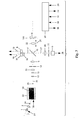
- Fig. 1 is an exploded top view of a 3-D sensor.
- Fig. 2 is an exploded top view of a 3-D sensor.
- Fig. 3 is an exploded top view of a 3-D sensor.
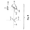
- Fig. 4 is an exploded top view of an alternative embodiment for projecting optical energy onto a target being sensed.
- Fig. 5a is an exploded top view of an embodiment of the present invention for detecting an output from a target being sensed that removes wavelength dependent reflectivity from the depth calculation.
- Fig.5b is an exploded top view of an alternative embodiment for detecting an output from a target being sensed that removes wavelength dependent reflectivity from the depth calculation.
- Fig. 5c is an exploded top view of an alternative embodiment for detecting an output from a target being sensed that removes wavelength dependent reflectivity from the depth calculation.
- Illumination source 1 produces broadband, high intensity optical energy.
- Illumination source 1 is, for example, a solid state superluminescent LED such as Model 861 30E-15 manufactured by EG&G Optoelectronics Division, a high intensity xenon short arc lamp, a tunable laser, or a pulsed laser having a broadband wavelength distribution.
- Illumination source 1 preferably is super bright and has approximately a 30 nm wavelength spread.
- the Model 861 30E-15 superluminescent LED has a center wavelength of 850 nm and ranges from 840 nm to 860 nm.
- An output of illumination source 1 is corrected for astigmatism and collimated by a lens 2.
- illumination source 1 is a superluminescent LED
- the output of source 1 in the absence of lens 2 is divergent, asymmetrical (with an elliptical cross-section), and quasi-diffraction-limited with a beam divergence that is greatest across the narrowest dimension of a cross-section of the LED emitter normal to an optical axis 7.
- the collimated output of lens 2 is passed through a quarter wave plate 3 to convert the highly linearly polarized output of illumination source 1 to circularly polarized light.
- All optics in this specification are preferably achromatic with the exception of an objective lens 22.
- the prepared beam emerging from quarter wave plate 3 is collimated, with the beam cross section filling an input window of an acousto-optic (AO) modulator 4.
- Modulator 4 contains a photoelastic crystal 10.
- An acoustic wave propagating in crystal 10 varies the index of refraction of crystal 10.
- Crystal 10 then acts as a diffraction grating, causing the incident beam to deflect as a function of the acoustic wavelength.
- the acoustic wavelength is determined by a radio frequency (RF) drive signal 11.
- RF radio frequency
- Crystal 10 is also wavelength dispersive. That is, in addition to its deflection angle being controlled by RF drive signal 11, the deflection angle of an incident beam is also directly proportional to an optical wavelength of the incident beam.
- the beam emerging from modulator 4 is shaped by a lens 12 and a lens 13.
- lens 12 and lens 13 are cylindrical lenses or have cylindrical elements.
- the shaped beam is focused onto a pinhole 14 by a lens 23.
- the dispersion of the beam focuses different wavelengths on pinhole 14 at different times.
- the beam that emerges from pinhole 14 contains a sequence of wavelengths as a function of time.
- pinhole 14 acts as a gate for the modulated beam, letting a particular wavelength, or color, through the gate at a particular time.
- the sequence of wavelengths is collimated by a lens 9.
- the collimated beam is incident on a beamsplitter 15. Beamsplitter 15 is wavelength and polarization insensitive. A first portion of the beam is transmitted through beamsplitter 15 to an objective lens 22.
- a second portion of the beam is reflected upward in the figure by beam splitter 15 onto an optical axis 17.
- Optical axis 17 leads to side by side detectors 8 and 31.
- a filter 16 is interposed in optical axis 17 in front of detector 31, but not in front of detector 8.
- Filter 16 is a bandpass filter matched to the optical spectrum of illumination source 1.
- Filter 16 produces a sharp pulse when the optical energy incident on filter 16 matches a particular synchronization point, thereby allowing two-point calibration.
- Detector 31 outputs a beam edge calibration signal 18.
- Signal 18 is used by signal processing electronics 20 to establish a precise time base for analysis of the received target energy.
- Detector 8 outputs a beam amplitude calibration signal 19 that describes an amplitude of received light as a function of time.
- Signal 19 is used by signal processing electronics 20 to monitor, and therefore minimize via feedback, combined effects of the variable energy level emitted by illumination source 1 as a function of wavelength, variable diffractive efficiency of modulator 4 as a function of wavelength, and any non-uniformity of transmissive wavelength response in collimation lens 2, quarter wave plate 3, modulator 4, lens 12, lens 13, lens 23, and lens 9.
- one objective is to keep the intensity of the light constant. If the distribution of the intensity of the light versus the wavelength produced by illumination source 1 is Gaussian, increasing the current to illumination source 1 at either end of the scanning range evens out the intensity at all wavelengths.
- Signal 19 is used by signal processing electronics 20 to normalize the response of the sensor to achieve uniform sensitivity across the optical bandwidth of illumination source 1. Signal 19 is also used by signal processing electronics 20 to regulate a drive signal 24 for illumination source 1, thereby minimizing temporal variation in the output of illumination source 1.
- Objective lens 22 projects the first portion of the beam onto a target 6.
- objective lens 22 is a diffractive objective lens to establish a distinct focal plane 100 for each illumination wavelength. If, for example, objective lens 22 has a focal length of 100 mm, the total depth of focus across the wavelengths varies by 3.5 mm.
- objective lens 22 establishes a temporally scanned focal point for which each range corresponds to a different transmitted wavelength. Longer wavelengths are focused closer to objective lens 22 and shorter wavelengths are focused farther away.
- Objective lens 22 is preferably fabricated by etching a surface of the lens to create a surface relief hologram (binary optic), by exposing an emulsion to create a volume hologram, or by manufacturing a micro-Fresnel lens (MFL).
- a suitable objective lens 22 is custom-manufactured by companies such as Teledyne Brown Engineering using techniques such as ion milling or reactive ion etching.
- a positioner 25 establishes a coarse location in range of the scanned depth-of-field by mechanically positioning objective lens 22.
- the focused light reflected from target 6 is collimated since it is reflected from a point.
- the reflected light is returned through objective lens 22 and reflected by beamsplitter 15 along an optical axis 21.
- the light is then focused onto a pinhole 27 by a lens 26.
- the light passing through pinhole 27 is incident on a detector 5.
- Lens 26 has negligible chromatic dispersion.
- Lenses 9, 22, and 26 preferably are approximately the same size.
- Pinhole 27 passes only the reflected light from the central maximum of the diffraction pattern of objective lens 22.
- the light that passes through pinhole 27 exhibits a high degree of wavelength dispersion. This wavelength dispersion is a function of the distance from objective lens 22 of the particular point on the target from which the light is being reflected.
- Detector 5 is preferably a high gain avalanche photodiode (APD) or a silicon PIN diode in a current integrating mode. Detector 5 outputs a signal 28 which consists of a pulse whose temporal centroid corresponds to the distance between objective lens 22 and the point on target 6. The temporal width of this pulse is approximately proportional to the depth-of-focus of objective lens 22.
- APD avalanche photodiode
- silicon PIN diode in a current integrating mode.
- Detector 5 outputs a signal 28 which consists of a pulse whose temporal centroid corresponds to the distance between objective lens 22 and the point on target 6. The temporal width of this pulse is approximately proportional to the depth-of-focus of objective lens 22.
- An example of the calculation to determine the height of the peak of a pulse includes:
- FIG. 2 an alternative embodiment is shown which differs from the embodiment of Fig. 1 by the addition of a diffraction grating 29 between photoelastic crystal 10 and lens 12 to improve the resolution of the sensor shown in Fig. 1.
- Diffraction grating 29 spatially disperses the broadband optical wavelengths produced by illumination source 1.
- the spatial dispersion from diffraction grating 29 is in addition to the spatial dispersion from modulator 4.
- Combining modulator 4 and diffraction grating 29 increases a range of beam deflection angles for the optical bandwidth of illumination source 1.
- the light that passes through pinhole 14 therefore exhibits increased temporal wavelength resolution.
- the increased temporal wavelength resolution results in increased measurement resolution of the target range by signal processing electronics 20.
- a wavelength-dispersing prism (not shown) is optionally used in place of diffraction grating 29.
- FIG. 3 an alternative embodiment is shown which differs from the embodiment of Fig. 2 by the substitution of a tunable filter 32, a crystal 33, and a signal 36 in place of modulator 4, crystal 10, and signal 11, respectively.
- two polarizers 34 and 35 are added and diffraction grating 29 is removed.
- the collimated output of lens 2 passes through polarizer 34, thereby refining the strongly linearly polarized output of LED illumination source 1 to a uniform linear polarization for all wavelengths.
- all optics are achromatic.
- the prepared beam emerging from polarizer 34 is incident upon tunable filter 32.
- Tunable filter 32 contains an anisotropic, birefringent acousto-optic (AO) crystal 33.
- AO acousto-optic
- an optical wavelength transmitted by crystal 33 varies as a function of a frequency of the acoustic wave.
- Uniformly polarized broadband incident illumination emerges from tunable filter 32 with a range of polarizations corresponding to a range of optical wavelengths.
- Polarizer 35 also known as an analyzer, selectively transmits only that light with a correctly oriented polarization. In practice, the light transmitted by the polarizer 35 is effectively monochromatic.
- Signal 36 establishes the frequency of the acoustic wave, thereby permitting tunable control of the wavelength passed by polarizer 35.
- the output of polarizer 35 contains a sequence of wavelengths as a function of time.
- pinhole 14 serves the dual function of wavelength selection and spatial filtering.
- pinhole 14 serves only as a spatial filter while tunable filter 32 accomplishes wavelength selection.
- an alternative to objective lens 22 in each embodiment includes a lens element 22a which is a Fresnel or diffractive mirror which changes its focal length depending on the wavelength.
- the light beam is deflected according to an angle between the illuminating beam and the normal to the mirror surface of lens element 22a.
- a positioner 25 moves along a normal to a target 6 to establish a coarse range location of the scanned depth-of field by mechanically positioning lens element 22a.
- lens element 22a is rotatable along axis 30, thereby causing the sampling beam to scan across the surface of target 6.
- lens element 22a is rotated instead of moving the sensor or the target.
- target 6 has wavelength sensitive reflectivity in the energy band used to perform the depth measurement. It is therefore desirable to use a means for compensating that removes the wavelength sensitive reflectivity from the depth calculation.
- a beamsplitter 102 diverts some of the optical energy, preferably half, to a central stop 101.
- Central stop 101 acts as an inverse pinhole, blocking that portion of the optical energy that is precisely focused on it.
- the optical energy blocked by central stop 101 equals the optical energy passed through pinhole 27.
- a detector 105 detects that optical energy that passes central stop 101, which equals the optical energy not passed by pinhole 27.
- Detector 105 outputs a signal 128 to signal processing electronics 20.
- Signal processing electronics 20 finds an instant of time within the sweep when a ratio of the amplitude of the output of detector 5 to the amplitude of the output of detector 105 is at its maximum.
- the energy passed through pinhole 27 is a result of the light being reflected off target 6 due to target 6 being at the focal point of objective lens 22 rather than being a result of the light reflected off target 6 due to a particular wavelength sensitive reflectivity.
- a calibrated depth for the wavelength transmitted at this instant of time therefore corresponds to the depth of the surface of target 6 since the ratio depends only upon the focus to pinhole 27 and is independent of the reflectivity of target 6.
- detectors 5 and 105 optionally are reduced by adding field lenses (not shown) between pinhole 27 and detector 5 and between central stop 101 and detector 105.
- an alternative embodiment for removing the wavelength reflectivity from the depth calculation replaces pinhole 27 with a detector 115 with a pinhole in it.
- This embodiment avoids the energy lost by beamsplitter 102 shown in Fig. 5a.
- Detector 115 directly detects and outputs signal 128 representing the energy not passing through the pinhole.
- Signal 128 is used in this embodiment the same as previously described for the embodiment of Fig. 5a.
- Fig. 5c an alternative embodiment is shown which also avoids beamsplitter losses while removing the wavelength reflectivity from the depth calculation.
- Pinhole 27 of Fig. 5a is replaced by a mirrored pinhole 127 which reflects that portion of optical energy not passing through the pinhole.
- Detector 105 and signal 128 are used as previously described in the embodiment of Fig. 5a.
- the peaking of the ratio of the signal from detector 5 divided by the signal from detectors 105 or 115 corresponds to the range of the surface of target 6 as indicated by the best focus of the light incident on target 6.
- a ratio of focused color light to unfocused color light is obtained.
- the unfocused color light is detected by detectors 105 or 115. Comparing the ratio of the focused light to the unfocused light prevents obtaining false readings from some color sensitive characteristic of target 6.
- the principle embodied in the separation methods of the embodiments of Figs. 5a, 5b, and 5c is used to remove sensitivity to target color vs. reflectivity variations from the embodiments of Figs. 1-3 by separating the light leaving lens 26 into two paths.
- One path includes only light passing through pinhole 27.
- the other path includes only light passing around pinhole 27.
Description
- This invention relates to an apparatus and method for three dimensional (3-D) vision sensing and measurement. In particular, this invention relates to an apparatus and method for measuring a distance an object is from a known location by using chromatic range discrimination techniques. Monochromatic light beams are reflected off of a target to produce a reflected beam which includes focused and unfocused portions. The ratio of focused to unfocused light from each monochromatic beam is used to determine the true distance of the target from the known location.
- High technology industries are in the midst of a manufacturing revolution. Established industries such as integrated circuit (IC) manufacturing, electronics assembly, and precision metrology are facing unrelenting customer requirements for increasing and unprecedented levels of precision and speed. Emerging technologies such as precision mechanical assembly, opto-electronics assembly, and micro electromechanical systems (MEMS) will demand new capabilities that are a generation ahead of current and near-term commercial technology. While the discussion that follows focuses on a case study of semiconductor industry requirements, the technology that is described is suitable for a broad range of applications in both established and emerging industries.
- The semiconductor industry has experienced a decade of unprecedented growth and technological advancements. Continual advances in circuit complexity and feature miniaturization have resulted in a requirement for substantially increased densities of input/output (I/O) leads. As a result, surface mount technology (SMT) packaging has largely replaced the traditional through-hole IC package. SMT leads, such as those on quad flat packs (QFP's), are soldered directly to connection pads on a surface of a circuit board, thereby permitting increased density of leads and a smaller device footprint. Recently, the new ball grid array (BGA) package has expanded the SMT class of devices. BGA replaces the peripheral SMT leads with a matrix of solder balls on the underside of the device. Future trends will extend the SMT concept to direct-attach methods such as flip chips, in which the connection bumps are integral to the wafer.
- These new packaging technologies present significant challenges to device manufacturers. For SMT devices, the increased density of connections means that SMT leads must be significantly smaller than the leads of through hole devices. The physical fragility of the leads is a major concern. Any lead deformation can result in an inability to solder correctly the device to the board. Since test probes can temporarily deflect a bad lead and make a device test electrically good when it is physically bad, lead deformations are not always discovered by automated electrical test equipment. For BGA and flip chip devices, the solder balls and connection bumps must be precisely sized and located in order to mate properly with the corresponding pads on the printed circuit (PC) board.
- A device's ensemble of SMT leads, BGA solder balls, or flip chip connection bumps is a 3-D structure which may exhibit monostable or bistable seating on a board. The ensemble may or may not be within acceptable tolerances for successful soldering during board assembly. Typical inspections of SMT devices with peripheral leads include checks of coplanarity, pin spread, pin width, gap width, true position spread, true position span, and lead angle. A typical inspection of a BGA device includes checks of coplanarity, true position error, pitch, ball diameter, and board warpage. The evolving requirements for flip chip devices are expected to include similar geometric requirements with substantially higher accuracies required than are needed for today's BGA's.
- The accuracies required by manufacturers are between 5 µm (.0002") and 12.5 µm (.0005") for measurement of SMT device coplanarity, pin spread, pin width, pin gap, true position spread, and true position span. Current BGA technology demands similar accuracies. Near-term trends in BGA technology (mini BGA and micro BGA packages) and flip chip technology will inevitably demand accuracies of 1 µm or better. This requirement calls for an order of magnitude improvement in accuracy over current capabilities.
- A number of commercial lead inspection systems use 2-D machine vision technology. Rather than measure the 3-D lead geometry directly, 2-D systems infer the 3-D shape from 2-D shadows. Because 2-D systems can only infer the true 3-D geometry from projections of that geometry, they are limited in their ability to characterize adequately the critical parameters of SMT leads. In addition, 2-D systems often seek to achieve adequate throughput by using multiple cameras. However, multiple cameras are susceptible to consequential calibration drift and accuracy degradation. Finally, all 2-D systems require extensive device handling that reduces throughput and damages the devices.
- Other commercial systems use 3-D machine vision such as disclosed in U.S. Patents 4,238,147, 4,590,367, 4,529,316, 4,594,001 and 4,991,968. Typical 3-D machine vision sensors are based on the well-established principle of structured-light optical triangulation. The object (e.g., SMT lead or BGA ball) is illuminated by a scanned, focused laser source. The reflected energy is captured by an offset camera. The known spatial relationship between the illumination source and the camera enables an accurate 3-D measurement to be computed. The combination of camera and structured light projector is a 3-D sensor.
- It is desirable to enhance the familiar optical triangulation method to accommodate the impending high-resolution, high-throughput requirements. One technique for improving the resolution of optical triangulation is to increase the angular separation between transmitter and receiver. However, this improvement is incremental at best, only applies to one dimension (range resolution), and is achieved at the penalty of increased susceptibility to occlusion of the viewed surface by neighboring surfaces.
- Another potential enhancement is to improve both the range resolution and lateral resolution by reducing a focused spot size of a transmitted laser beam. The spot size is directly proportional to the product of the f-number of the projection optics (as viewed from the target) and the laser wavelength. The projection optics may be improved incrementally, but not by an order of magnitude while maintaining depth-of-field.
- Achieving shorter wavelengths and higher resolution is possible using higher frequency illumination sources. Current optical triangulation systems operate in the near infrared (800-900 nm wavelength). The shorter wavelengths of interest are in the deep ultraviolet (<300 nm). Unfortunately, the ultraviolet (UV) region is characterized by a lack of low-cost, solid-state illumination sources, very low photodetector sensitivity, and the degradation of optical components with use. UV wavelengths present major practical problems for a commercial, high duty-cycle inspection system.
- A recently popular technique for high-accuracy optical measurement on semiconductor wafer surfaces, known as laser confocal microscopy, utilizes a diffraction-limited, monochromatic spot of light projected on a target surface. A pinhole in the focal plane of the receiver optics is mechanically translated in range. The returned energy through the pinhole is maximum when the focal plane coincides with the target surface image, thus enabling measurement of the target range. This technique is capable of submicron range resolution. However, it is a very slow process due to the mechanical servoing of a minimal depth-of-focus across the total depth-of-field where the target is to be found. Microscope calibration is difficult. The moving parts can wear with use, causing maintenance downtime.
- Another recent technique uses the dispersion characteristics of a diffractive micro-Fresnel lens (MFL) in a spectrometer as outlined in "Spectrometer Employing a Micro-Fresnel Lens", Optical Engineering Vol. 34 No. 2, pp. 584-588 (February 1995). MFL's generally have large chromatic aberration. MFL's therefore transform the incident light spectrum into an intensity distribution along the optical axis. Different colors (wavelengths) have different focal lengths. A movable pinhole is positioned between a photodetector and a MFL. The light that passes through the pinhole is detected by the photodetector, which outputs a current corresponding to the light intensity of the light focused at the pinhole. An intensity distribution is obtained by moving the pinhole. The distances between the MFL and the pinhole passing focused light directly correspond to the wavelengths of the incident light. The spectrum of the incident light is thus obtained.
- The above technique of dispersing a beam (i.e. with a Fresnel lens) and measuring range based upon a detection of a peak in the returned light is also discussed in a publication entitled "Longitudinally Dispersive Profilometer", Pure and Applied Optics, Vol. 4, No. 3, pp. 219-228 (May 1995). A similar optical surface profiler is disclosed in "Optical Surface Profiler Transducer", Optical Engineering, Vol. 27, No. 2, pp. 135-142 (Feb. 1988).
- Another technique uses three chromatic filters in order to determine distance as outlined in "Three-dimensional image sensing by chromatic confocal microscopy, Applied Optics, Vol. 33, No. 10, pp. 1838-1843 (April 1994). Light is reflected off of a target through a chromatically aberrated objective lens. Multiple wavelengths of light are simultaneously reflected off of the targets surface and directed to three different chromatic filters which function similar to the human eye. Each chromatic filter is used to discriminate a different color. The distance of the target from a known location is deduced from the relative amount of light received through each of three chromatic filters.
- Another way of determining a range calculation is outlined in U.S. Patent No. 3,815,409. According to the disclosure, a chirped frequency modulated sound wave can be passed through a dispersive lens that has varying focal lengths with frequency. Each frequency is focused at a different depth to the object. A time delay is measured from the transmission of the sound wave until a reception of a reflected sound wave into a transducer. The time delay corresponds to a particular depth to the object.
- Conversely, if the wavelength of the incident light (and its attendant focal length) is known, the distance between the pinhole and the MFL is readily determined. An adaptation of this principle is used in the present invention.
- It is an object of the present invention to overcome the drawbacks and limitations of the prior art.
- It is another object of the present invention to provide a non-triangulation approach to optical 3-D measurement.
- It is a further object of the present invention to provide a fast, efficient method and apparatus for sensing and measuring ranges on the order of a micron.
- It is a still further object of the present invention to provide an optical ranging sensor that compensates for wavelength dependent reflectivity of a target.
- The above and other objectives are realized by an apparatus and method in which a system projector includes a polychromatic incoherent illumination source. The system projector also includes an illumination modulator which establishes a time-varying illumination wavelength. The system projector further includes a diffractive lens which establishes a continuum of focal planes corresponding to the wavelengths in the illumination spectrum.
- The present invention retains the high resolution capabilities of the confocal microscope and overcomes the deficiencies that prohibit the use of this technique in high-throughput, high duty-cycle industrial applications by replacing the mechanical scanning of a single focal plane with an illumination technique in which a continuum of focal planes encompasses a large depth-of-field. Signal processing electronics detect a location of a target surface with an accuracy exceeding a depth-of-focus of any individual focal plane. This technique results in rapid measurement that is configured to satisfy a wide range of high accuracy measurement requirements.
- The present invention is based on the principle of chromatic range discrimination. Conventional laser-based 3-D sensors use coherent monochromatic illumination. In contrast, the present invention uses broadband incoherent or broadband coherent illumination. Conventional laser-based 3-D sensors illuminate the depth-of-field via mechanical motion. In contrast, the present invention uses a chromatic range scanner to illuminate the depth-of-field electronically. Conventional laser-based 3-D triangulation sensors rely on the geometry of the entire sensor (transmitter and receiver) to achieve range resolution.
- Reconfiguring the sensor for different applications requiring different performance parameters often requires significant redesign. In contrast, the present invention is readily reconfigured using interchangeable objective lenses. Conventional laser-based 3-D triangulation sensors require that both transmitted and received rays be totally unimpeded, thus necessitating a large angular region between the sensor and the object remaining totally unobstructed. The present invention significantly reduces the occlusion limitations of high-accuracy optical triangulation sensors. Partial occlusion only slightly reduces the returned energy (i.e., slightly decreases the signal-to-noise ratio) and does not cause the sensor to fail to detect the object surface.
- Briefly stated, a three dimensional sensor includes an illumination source that produces broadband, high intensity optical energy. This optical energy includes a number of individual wavelength components. The individual wavelength components are impinged in a spot on a target. Dispersion is applied to the light reflected from the spot, either before target impingement, after target impingement, or both, whereby light of different colors is focused at different distances from the target. A maximum reflected wavelength, dependent on target range, is detected to determine the target range. In one embodiment, temporal modulation is applied to the light before target impingement. A stationary detector determines the target range by relating the maximum light received to the time it is received in order to determine the color received at that time. A detector array, or a linear position sensor, is employed to determine the transverse position of the maximum amplitude of the transversely dispersed beam. The transverse position, being related to a particular color, contains information from which the range to the target is determinable.
- The invention is defined in
claim 1. - Preferred aspects are referred to in claims 2-10.
- The above, and other objects, features and advantages of the present invention will become apparent from the following description read in conjunction with the accompanying drawings, in which like reference numerals designate the same elements.
- Fig. 1 is an exploded top view of a 3-D sensor.
- Fig. 2 is an exploded top view of a 3-D sensor.
- Fig. 3 is an exploded top view of a 3-D sensor.
- Fig. 4 is an exploded top view of an alternative embodiment for projecting optical energy onto a target being sensed.
- Fig. 5a is an exploded top view of an embodiment of the present invention for detecting an output from a target being sensed that removes wavelength dependent reflectivity from the depth calculation.
- Fig.5b is an exploded top view of an alternative embodiment for detecting an output from a target being sensed that removes wavelength dependent reflectivity from the depth calculation.
- Fig. 5c is an exploded top view of an alternative embodiment for detecting an output from a target being sensed that removes wavelength dependent reflectivity from the depth calculation.
- Referring to Fig. 1, a basic 3-D sensor is shown. The sensor uses acousto-optical beam deflection. An
illumination source 1 produces broadband, high intensity optical energy.Illumination source 1 is, for example, a solid state superluminescent LED such as Model 861 30E-15 manufactured by EG&G Optoelectronics Division, a high intensity xenon short arc lamp, a tunable laser, or a pulsed laser having a broadband wavelength distribution.Illumination source 1 preferably is super bright and has approximately a 30 nm wavelength spread. The Model 861 30E-15 superluminescent LED has a center wavelength of 850 nm and ranges from 840 nm to 860 nm. - An output of
illumination source 1 is corrected for astigmatism and collimated by alens 2. For example, ifillumination source 1 is a superluminescent LED, the output ofsource 1 in the absence oflens 2 is divergent, asymmetrical (with an elliptical cross-section), and quasi-diffraction-limited with a beam divergence that is greatest across the narrowest dimension of a cross-section of the LED emitter normal to an optical axis 7. Since the output of the superluminescent LED is highly linearly polarized, the collimated output oflens 2 is passed through aquarter wave plate 3 to convert the highly linearly polarized output ofillumination source 1 to circularly polarized light. Using circularly polarized light avoids potential uneven effects of linearly polarized light in the optics used in the invention. All optics in this specification (unless otherwise stated) are preferably achromatic with the exception of anobjective lens 22. - The prepared beam emerging from
quarter wave plate 3 is collimated, with the beam cross section filling an input window of an acousto-optic (AO)modulator 4.Modulator 4 contains aphotoelastic crystal 10. An acoustic wave propagating incrystal 10 varies the index of refraction ofcrystal 10.Crystal 10 then acts as a diffraction grating, causing the incident beam to deflect as a function of the acoustic wavelength. The acoustic wavelength is determined by a radio frequency (RF) drivesignal 11. The incident beam deflects to a direction around anoptical axis 30. -
Crystal 10 is also wavelength dispersive. That is, in addition to its deflection angle being controlled byRF drive signal 11, the deflection angle of an incident beam is also directly proportional to an optical wavelength of the incident beam.Modulator 4 both disperses the individual wavelength components ofbroadband illumination source 1 and deflects the dispersed wavelengths. If denotes the diffraction angle ofmodulator 4 measured in radians, λ denotes the optical wavelength measured in meters, F denotes the frequency ofRF drive signal 11 measured in Hertz, and v denotes the acoustic velocity ofcrystal 10 measured in meters per second, then for any λ and F, = λ * F ÷ v . - The beam emerging from
modulator 4 is shaped by alens 12 and alens 13. In some cases,lens 12 andlens 13 are cylindrical lenses or have cylindrical elements. The shaped beam is focused onto apinhole 14 by alens 23. With a swept or stepped RF wavelength ofRF drive signal 11, the dispersion of the beam focuses different wavelengths onpinhole 14 at different times. Asmodulator 4 deflects the dispersed wavelengths acrosspinhole 14, the beam that emerges frompinhole 14 contains a sequence of wavelengths as a function of time. In other words, pinhole 14 acts as a gate for the modulated beam, letting a particular wavelength, or color, through the gate at a particular time. The sequence of wavelengths is collimated by alens 9. The collimated beam is incident on abeamsplitter 15.Beamsplitter 15 is wavelength and polarization insensitive. A first portion of the beam is transmitted throughbeamsplitter 15 to anobjective lens 22. - A second portion of the beam is reflected upward in the figure by
beam splitter 15 onto anoptical axis 17.Optical axis 17 leads to side byside detectors filter 16 is interposed inoptical axis 17 in front ofdetector 31, but not in front ofdetector 8.Filter 16 is a bandpass filter matched to the optical spectrum ofillumination source 1.Filter 16 produces a sharp pulse when the optical energy incident onfilter 16 matches a particular synchronization point, thereby allowing two-point calibration.Detector 31 outputs a beamedge calibration signal 18.Signal 18 is used bysignal processing electronics 20 to establish a precise time base for analysis of the received target energy. -
Detector 8 outputs a beamamplitude calibration signal 19 that describes an amplitude of received light as a function of time.Signal 19 is used bysignal processing electronics 20 to monitor, and therefore minimize via feedback, combined effects of the variable energy level emitted byillumination source 1 as a function of wavelength, variable diffractive efficiency ofmodulator 4 as a function of wavelength, and any non-uniformity of transmissive wavelength response incollimation lens 2,quarter wave plate 3,modulator 4,lens 12,lens 13,lens 23, andlens 9. For example, one objective is to keep the intensity of the light constant. If the distribution of the intensity of the light versus the wavelength produced byillumination source 1 is Gaussian, increasing the current toillumination source 1 at either end of the scanning range evens out the intensity at all wavelengths.Signal 19 is used bysignal processing electronics 20 to normalize the response of the sensor to achieve uniform sensitivity across the optical bandwidth ofillumination source 1.Signal 19 is also used bysignal processing electronics 20 to regulate adrive signal 24 forillumination source 1, thereby minimizing temporal variation in the output ofillumination source 1. -
Objective lens 22 projects the first portion of the beam onto atarget 6. Preferablyobjective lens 22 is a diffractive objective lens to establish a distinctfocal plane 100 for each illumination wavelength. If, for example,objective lens 22 has a focal length of 100 mm, the total depth of focus across the wavelengths varies by 3.5 mm. In conjunction with the previously discussed optical elements,objective lens 22 establishes a temporally scanned focal point for which each range corresponds to a different transmitted wavelength. Longer wavelengths are focused closer toobjective lens 22 and shorter wavelengths are focused farther away.Objective lens 22 is preferably fabricated by etching a surface of the lens to create a surface relief hologram (binary optic), by exposing an emulsion to create a volume hologram, or by manufacturing a micro-Fresnel lens (MFL). A suitableobjective lens 22 is custom-manufactured by companies such as Teledyne Brown Engineering using techniques such as ion milling or reactive ion etching. Apositioner 25 establishes a coarse location in range of the scanned depth-of-field by mechanically positioningobjective lens 22. - The focused light reflected from
target 6 is collimated since it is reflected from a point. The reflected light is returned throughobjective lens 22 and reflected bybeamsplitter 15 along anoptical axis 21. The light is then focused onto apinhole 27 by alens 26. The light passing throughpinhole 27 is incident on adetector 5.Lens 26 has negligible chromatic dispersion.Lenses Pinhole 27 passes only the reflected light from the central maximum of the diffraction pattern ofobjective lens 22. The light that passes throughpinhole 27 exhibits a high degree of wavelength dispersion. This wavelength dispersion is a function of the distance fromobjective lens 22 of the particular point on the target from which the light is being reflected.Detector 5 is preferably a high gain avalanche photodiode (APD) or a silicon PIN diode in a current integrating mode.Detector 5 outputs asignal 28 which consists of a pulse whose temporal centroid corresponds to the distance betweenobjective lens 22 and the point ontarget 6. The temporal width of this pulse is approximately proportional to the depth-of-focus ofobjective lens 22. - An example of the calculation to determine the height of the peak of a pulse includes:
- 1) Compute an amplitude that is 70% of the height of the peak.
- 2) Find the 70% amplitude at the beginning and end of the pulse to obtain two times.
- 3) Average these two times to obtain the centroid.
- 4) Use standard interpolation techniques in
signal processing electronics 20 to locate the pulse centroid to a small fraction of the wavelength resolution. -
- Referring to Fig. 2, an alternative embodiment is shown which differs from the embodiment of Fig. 1 by the addition of a
diffraction grating 29 betweenphotoelastic crystal 10 andlens 12 to improve the resolution of the sensor shown in Fig. 1. -
Diffraction grating 29 spatially disperses the broadband optical wavelengths produced byillumination source 1. The spatial dispersion fromdiffraction grating 29 is in addition to the spatial dispersion frommodulator 4. Combiningmodulator 4 anddiffraction grating 29 increases a range of beam deflection angles for the optical bandwidth ofillumination source 1. The light that passes throughpinhole 14 therefore exhibits increased temporal wavelength resolution. The increased temporal wavelength resolution results in increased measurement resolution of the target range bysignal processing electronics 20. A wavelength-dispersing prism (not shown) is optionally used in place ofdiffraction grating 29. - Referring to Fig. 3, an alternative embodiment is shown which differs from the embodiment of Fig. 2 by the substitution of a
tunable filter 32, acrystal 33, and asignal 36 in place ofmodulator 4,crystal 10, and signal 11, respectively. In addition, twopolarizers diffraction grating 29 is removed. The collimated output oflens 2 passes throughpolarizer 34, thereby refining the strongly linearly polarized output ofLED illumination source 1 to a uniform linear polarization for all wavelengths. With the exception ofobjective lens 22, all optics are achromatic. The prepared beam emerging frompolarizer 34 is incident upontunable filter 32.Tunable filter 32 contains an anisotropic, birefringent acousto-optic (AO)crystal 33. When an acoustic wave is propagated inAO crystal 33, an optical wavelength transmitted bycrystal 33 varies as a function of a frequency of the acoustic wave. Uniformly polarized broadband incident illumination emerges fromtunable filter 32 with a range of polarizations corresponding to a range of optical wavelengths.Polarizer 35, also known as an analyzer, selectively transmits only that light with a correctly oriented polarization. In practice, the light transmitted by thepolarizer 35 is effectively monochromatic.Signal 36 establishes the frequency of the acoustic wave, thereby permitting tunable control of the wavelength passed bypolarizer 35. Therefore, the output ofpolarizer 35 contains a sequence of wavelengths as a function of time. With the exception ofpinhole 14, all other elements function as previously described. In Figs. 1 and 2,pinhole 14 serves the dual function of wavelength selection and spatial filtering. In Fig. 3,pinhole 14 serves only as a spatial filter whiletunable filter 32 accomplishes wavelength selection. - Referring to Fig.4, an alternative to
objective lens 22 in each embodiment includes alens element 22a which is a Fresnel or diffractive mirror which changes its focal length depending on the wavelength. In such a case, the light beam is deflected according to an angle between the illuminating beam and the normal to the mirror surface oflens element 22a. Apositioner 25 moves along a normal to atarget 6 to establish a coarse range location of the scanned depth-of field by mechanically positioninglens element 22a. - In an alternative embodiment,
lens element 22a is rotatable alongaxis 30, thereby causing the sampling beam to scan across the surface oftarget 6. Thus,lens element 22a is rotated instead of moving the sensor or the target. - In certain applications target 6 has wavelength sensitive reflectivity in the energy band used to perform the depth measurement. It is therefore desirable to use a means for compensating that removes the wavelength sensitive reflectivity from the depth calculation.
- The present invention will now be discussed with reference to Figs. 5a - 5c.
- Referring to Fig. 5a, an arrangement for compensating for wavelength sensitive reflectivity of
target 6 is shown. After the light reflected fromtarget 6 is focused bylens 26 as shown in Figs. 1, 2, or 3, abeamsplitter 102 diverts some of the optical energy, preferably half, to acentral stop 101. Central stop 101 acts as an inverse pinhole, blocking that portion of the optical energy that is precisely focused on it. The optical energy blocked bycentral stop 101 equals the optical energy passed throughpinhole 27. Adetector 105 detects that optical energy that passescentral stop 101, which equals the optical energy not passed bypinhole 27.Detector 105 outputs asignal 128 to signalprocessing electronics 20.Signal processing electronics 20 finds an instant of time within the sweep when a ratio of the amplitude of the output ofdetector 5 to the amplitude of the output ofdetector 105 is at its maximum. - At this instant of time, the energy passed through
pinhole 27 is a result of the light being reflected offtarget 6 due totarget 6 being at the focal point ofobjective lens 22 rather than being a result of the light reflected offtarget 6 due to a particular wavelength sensitive reflectivity. A calibrated depth for the wavelength transmitted at this instant of time therefore corresponds to the depth of the surface oftarget 6 since the ratio depends only upon the focus to pinhole 27 and is independent of the reflectivity oftarget 6. - The sizes of
detectors pinhole 27 anddetector 5 and betweencentral stop 101 anddetector 105. - Referring to Fig. 5b, an alternative embodiment for removing the wavelength reflectivity from the depth calculation replaces
pinhole 27 with adetector 115 with a pinhole in it. This embodiment avoids the energy lost bybeamsplitter 102 shown in Fig. 5a.Detector 115 directly detects and outputs signal 128 representing the energy not passing through the pinhole.Signal 128 is used in this embodiment the same as previously described for the embodiment of Fig. 5a. - Referring to Fig. 5c, an alternative embodiment is shown which also avoids beamsplitter losses while removing the wavelength reflectivity from the depth calculation.
Pinhole 27 of Fig. 5a is replaced by a mirroredpinhole 127 which reflects that portion of optical energy not passing through the pinhole.Detector 105 and signal 128 are used as previously described in the embodiment of Fig. 5a. - In each embodiment shown in Figs. 5a-5c, the peaking of the ratio of the signal from
detector 5 divided by the signal fromdetectors target 6 as indicated by the best focus of the light incident ontarget 6. In other words, a ratio of focused color light to unfocused color light is obtained. The unfocused color light is detected bydetectors target 6. - The principle embodied in the separation methods of the embodiments of Figs. 5a, 5b, and 5c is used to remove sensitivity to target color vs. reflectivity variations from the embodiments of Figs. 1-3 by separating the
light leaving lens 26 into two paths. One path includes only light passing throughpinhole 27. The other path includes only light passing aroundpinhole 27.
Claims (10)
- A sensor, comprising:characterised by:a source beam (30) from a polychromatic electromagnetic radiation source (1);first means for processing said source beam to produce an incident beam;said incident beam being projected on a target;a reflected beam (21) reflected from a surface of said target; andmeans for collecting said reflected beam;said first means for processing including means (4, 32) for modulating said source beam by wavelength over time, to produce said incident beam;said incident beam is projected along an incident beam axis (30);said incident beam being a time-modulated beam such that said incident beam has a first wavelength at a first time and a second wavelength at a second time;means for focusing said incident beam onto said target, whereby said first wavelength and said second wavelength are wavelengths which are focused at different distances along said incident beam axis from a known location;means for detecting said reflected beam at said first and second time;said reflected beam having a focused portion and a unfocused portion; andsecond means for processing said reflected beam to determine a distance of said target (6) from said known location by comparing ratios of said focused to unfocused portions at each said time.
- A sensor according to claim 1, said first means for processing further comprising:
means for establishing a precise time base (16,31) of said incident beam. - A sensor according to claim 1, wherein said means for focusing includes one of a diffraction-limited lens (22), an objective lens, a diffractive mirror (22a), and a micro-Fresnel lens (22a).
- A sensor according to claim 1, wherein said means for modulating includes an acousto-optic modulator (4).
- A sensor according to claim 1, wherein said means for modulating includes a photoelastic crystal (10) and a diffraction grating (29).
- A sensor according to claim 1, wherein said means for modulating includes a tunable filter (32) and a birefringent acousto-optic crystal (33).
- A sensor according to claim 1, wherein said means for detecting and said second means for processing said reflected beam includes means for dispersing said reflected beam.
- A sensor according to claim 1, further comprising means (8) for determining an amplitude of said incident beam as a function of time.
- A sensor according to claim 1, further comprising:said means (5a - 5c) for detecting said reflected beam being effective to detect said focused portion and said unfocused portion to produce signal amplitudes (28, 128) of said focused portion and said unfocused portion respectively; andmeans for determining the ratio of signal amplitudes.
- A sensor according to claim 1, wherein said means for detecting and interpolating said reflected beam includes one of a high-gain avalanche photodiode (5), a silicon PIN diode (5), a charge coupled device (5).
Priority Applications (1)
| Application Number | Priority Date | Filing Date | Title |
|---|---|---|---|
| EP99126196A EP0997748B1 (en) | 1995-07-31 | 1996-07-20 | Chromatic optical ranging sensor |
Applications Claiming Priority (2)
| Application Number | Priority Date | Filing Date | Title |
|---|---|---|---|
| US509534 | 1995-07-31 | ||
| US08/509,534 US5790242A (en) | 1995-07-31 | 1995-07-31 | Chromatic optical ranging sensor |
Related Child Applications (1)
| Application Number | Title | Priority Date | Filing Date |
|---|---|---|---|
| EP99126196A Division EP0997748B1 (en) | 1995-07-31 | 1996-07-20 | Chromatic optical ranging sensor |
Publications (2)
| Publication Number | Publication Date |
|---|---|
| EP0762143A1 EP0762143A1 (en) | 1997-03-12 |
| EP0762143B1 true EP0762143B1 (en) | 2000-10-04 |
Family
ID=24027029
Family Applications (2)
| Application Number | Title | Priority Date | Filing Date |
|---|---|---|---|
| EP96111721A Expired - Lifetime EP0762143B1 (en) | 1995-07-31 | 1996-07-20 | Chromatic optical ranging sensor |
| EP99126196A Expired - Lifetime EP0997748B1 (en) | 1995-07-31 | 1996-07-20 | Chromatic optical ranging sensor |
Family Applications After (1)
| Application Number | Title | Priority Date | Filing Date |
|---|---|---|---|
| EP99126196A Expired - Lifetime EP0997748B1 (en) | 1995-07-31 | 1996-07-20 | Chromatic optical ranging sensor |
Country Status (4)
| Country | Link |
|---|---|
| US (1) | US5790242A (en) |
| EP (2) | EP0762143B1 (en) |
| DE (2) | DE69610540T2 (en) |
| DK (1) | DK0762143T3 (en) |
Cited By (2)
| Publication number | Priority date | Publication date | Assignee | Title |
|---|---|---|---|---|
| DE102009001086A1 (en) * | 2009-02-23 | 2010-09-02 | Sirona Dental Systems Gmbh | Hand-held dental camera and method for 3D optical measurement |
| DE102008011057B4 (en) * | 2007-02-27 | 2020-12-10 | Disco Corp. | Measuring device for a workpiece held on a clamping table and a laser processing machine |
Families Citing this family (104)
| Publication number | Priority date | Publication date | Assignee | Title |
|---|---|---|---|---|
| US6073846A (en) * | 1994-08-17 | 2000-06-13 | Metrologic Instruments, Inc. | Holographic laser scanning system and process and apparatus and method |
| FR2761151B1 (en) * | 1997-03-21 | 1999-07-16 | Samuel Bucourt | OPTRONIC SYSTEM FOR NON-CONTACT DISTANCE MEASUREMENT OF A LIGHT SOURCE BY ANALYSIS OF THE WAVE POINT CURVATURE FROM IT |
| US6052190A (en) * | 1997-09-09 | 2000-04-18 | Utoptics, Inc. | Highly accurate three-dimensional surface digitizing system and methods |
| FR2780163B1 (en) * | 1998-06-18 | 2000-08-11 | Agence Spatiale Europeenne | INCOHERENT LASER DOPPLER TELESCOPY SYSTEM |
| US6518997B1 (en) * | 1998-08-05 | 2003-02-11 | National Semiconductor Corporation | Grid array inspection system and method |
| US11026768B2 (en) | 1998-10-08 | 2021-06-08 | Align Technology, Inc. | Dental appliance reinforcement |
| US6490027B1 (en) * | 1999-07-27 | 2002-12-03 | Suzanne K. Rajchel | Reduced noise optical system and method for measuring distance |
| US6400447B1 (en) * | 2000-03-11 | 2002-06-04 | Trimble Navigation, Ltd | Differentiation of targets in optical station based on the strength of the reflected signal |
| DE10018256A1 (en) * | 2000-04-13 | 2001-10-25 | Leica Microsystems | Double confocal scanning microscope |
| US6597712B2 (en) * | 2001-02-26 | 2003-07-22 | Hitachi, Ltd. | Laser diode module |
| JP2002252413A (en) * | 2001-02-26 | 2002-09-06 | Hitachi Ltd | Semiconductor laser module and optical system using the same |
| FR2824903B1 (en) * | 2001-05-21 | 2004-01-16 | Sciences Tech Ind De La Lumier | IMPROVEMENT OF METHODS AND DEVICES FOR MEASURING BY CONFOCAL IMAGING WITH EXTENDED CHROMATISM |
| US7081978B2 (en) * | 2003-03-17 | 2006-07-25 | Raytheon Company | Beam combining device for multi-spectral laser diodes |
| US9492245B2 (en) | 2004-02-27 | 2016-11-15 | Align Technology, Inc. | Method and system for providing dynamic orthodontic assessment and treatment profiles |
| US7317513B2 (en) * | 2004-07-15 | 2008-01-08 | Mitutoyo Corporation | Absolute distance measuring device |
| US7477401B2 (en) * | 2004-11-24 | 2009-01-13 | Tamar Technology, Inc. | Trench measurement system employing a chromatic confocal height sensor and a microscope |
| DE102005013076A1 (en) * | 2005-03-18 | 2006-10-05 | TRüTZSCHLER GMBH & CO. KG | Apparatus for removing the fiber material of textile fiber bales from spun goods, z. As cotton, chemical fibers and the like. |
| US7672527B2 (en) * | 2006-03-06 | 2010-03-02 | Northrop Grumman Corporation | Method and apparatus for chromatic correction of Fresnel lenses |
| DE102006026775B4 (en) * | 2006-06-07 | 2008-04-30 | Stiftung Für Lasertechnologien In Der Medizin Und Messtechnik An Der Universität Ulm | Method and device for characterizing moving surfaces |
| WO2008012706A2 (en) * | 2006-07-20 | 2008-01-31 | Koninklijke Philips Electronics N.V. | Multi-color biosensor |
| JP2010510485A (en) * | 2006-11-17 | 2010-04-02 | コーニンクレッカ フィリップス エレクトロニクス エヌ ヴィ | Self-mixing optical coherence detector without external beam splitter |
| WO2008124397A1 (en) | 2007-04-03 | 2008-10-16 | David Fishbaine | Inspection system and method |
| DE102007024075B4 (en) * | 2007-05-22 | 2022-06-09 | Leica Microsystems Cms Gmbh | Tunable acousto-optic filter element, adjustable light source, microscope and acousto-optic beam splitter |
| US7878805B2 (en) | 2007-05-25 | 2011-02-01 | Align Technology, Inc. | Tabbed dental appliance |
| US7812971B2 (en) * | 2007-06-28 | 2010-10-12 | Quality Vision International, Inc. | Multi color autofocus apparatus and method |
| US7808617B2 (en) * | 2007-09-17 | 2010-10-05 | Quality Vision International, Inc. | Dual resolution, dual range sensor system and method |
| US8738394B2 (en) | 2007-11-08 | 2014-05-27 | Eric E. Kuo | Clinical data file |
| US7554652B1 (en) * | 2008-02-29 | 2009-06-30 | Institut National D'optique | Light-integrating rangefinding device and method |
| US8108189B2 (en) | 2008-03-25 | 2012-01-31 | Align Technologies, Inc. | Reconstruction of non-visible part of tooth |
| US8092215B2 (en) | 2008-05-23 | 2012-01-10 | Align Technology, Inc. | Smile designer |
| US9492243B2 (en) | 2008-05-23 | 2016-11-15 | Align Technology, Inc. | Dental implant positioning |
| US8172569B2 (en) | 2008-06-12 | 2012-05-08 | Align Technology, Inc. | Dental appliance |
| US8152518B2 (en) | 2008-10-08 | 2012-04-10 | Align Technology, Inc. | Dental positioning appliance having metallic portion |
| US20100226114A1 (en) * | 2009-03-03 | 2010-09-09 | David Fishbaine | Illumination and imaging system |
| US8292617B2 (en) | 2009-03-19 | 2012-10-23 | Align Technology, Inc. | Dental wire attachment |
| US8765031B2 (en) | 2009-08-13 | 2014-07-01 | Align Technology, Inc. | Method of forming a dental appliance |
| US20110188116A1 (en) * | 2010-02-02 | 2011-08-04 | Nikolay Ledentsov Ledentsov | Device for generation of three-demensional images |
| US9211166B2 (en) | 2010-04-30 | 2015-12-15 | Align Technology, Inc. | Individualized orthodontic treatment index |
| US9241774B2 (en) | 2010-04-30 | 2016-01-26 | Align Technology, Inc. | Patterned dental positioning appliance |
| US9557574B2 (en) * | 2010-06-08 | 2017-01-31 | Microsoft Technology Licensing, Llc | Depth illumination and detection optics |
| CN102985788B (en) * | 2010-07-23 | 2015-02-11 | 丰田自动车株式会社 | Distance measurement device and distance measurement method |
| US9403238B2 (en) | 2011-09-21 | 2016-08-02 | Align Technology, Inc. | Laser cutting |
| US8587789B2 (en) | 2011-12-21 | 2013-11-19 | Mitutoyo Corporation | Chromatic point sensor compensation including workpiece material effects |
| US8587772B2 (en) | 2011-12-21 | 2013-11-19 | Mitutoyo Corporation | Chromatic point sensor configuration including real time spectrum compensation |
| US9375300B2 (en) | 2012-02-02 | 2016-06-28 | Align Technology, Inc. | Identifying forces on a tooth |
| US9220580B2 (en) | 2012-03-01 | 2015-12-29 | Align Technology, Inc. | Determining a dental treatment difficulty |
| US9414897B2 (en) | 2012-05-22 | 2016-08-16 | Align Technology, Inc. | Adjustment of tooth position in a virtual dental model |
| JP6044315B2 (en) * | 2012-12-12 | 2016-12-14 | オムロン株式会社 | Displacement measuring method and displacement measuring apparatus |
| US9261356B2 (en) | 2014-07-03 | 2016-02-16 | Align Technology, Inc. | Confocal surface topography measurement with fixed focal positions |
| US9439568B2 (en) | 2014-07-03 | 2016-09-13 | Align Technology, Inc. | Apparatus and method for measuring surface topography optically |
| US9261358B2 (en) | 2014-07-03 | 2016-02-16 | Align Technology, Inc. | Chromatic confocal system |
| US10772506B2 (en) | 2014-07-07 | 2020-09-15 | Align Technology, Inc. | Apparatus for dental confocal imaging |
| US9693839B2 (en) | 2014-07-17 | 2017-07-04 | Align Technology, Inc. | Probe head and apparatus for intraoral confocal imaging using polarization-retarding coatings |
| US9675430B2 (en) | 2014-08-15 | 2017-06-13 | Align Technology, Inc. | Confocal imaging apparatus with curved focal surface |
| US9660418B2 (en) | 2014-08-27 | 2017-05-23 | Align Technology, Inc. | VCSEL based low coherence emitter for confocal 3D scanner |
| US10449016B2 (en) | 2014-09-19 | 2019-10-22 | Align Technology, Inc. | Arch adjustment appliance |
| US9610141B2 (en) | 2014-09-19 | 2017-04-04 | Align Technology, Inc. | Arch expanding appliance |
| US9744001B2 (en) | 2014-11-13 | 2017-08-29 | Align Technology, Inc. | Dental appliance with cavity for an unerupted or erupting tooth |
| US9706094B2 (en) | 2014-12-05 | 2017-07-11 | National Security Technologies, Llc | Hyperchromatic lens for recording time-resolved phenomena |
| US10504386B2 (en) | 2015-01-27 | 2019-12-10 | Align Technology, Inc. | Training method and system for oral-cavity-imaging-and-modeling equipment |
| US10248883B2 (en) | 2015-08-20 | 2019-04-02 | Align Technology, Inc. | Photograph-based assessment of dental treatments and procedures |
| US9903757B1 (en) * | 2015-09-25 | 2018-02-27 | Hrl Laboratories, Llc | Active multi-spectral sensor |
| US10408676B2 (en) | 2015-10-01 | 2019-09-10 | Mission Support and Test Services, LLC | Long-pulse-width variable-wavelength chirped pulse generator and method |
| US11931222B2 (en) | 2015-11-12 | 2024-03-19 | Align Technology, Inc. | Dental attachment formation structures |
| US11554000B2 (en) | 2015-11-12 | 2023-01-17 | Align Technology, Inc. | Dental attachment formation structure |
| US11596502B2 (en) | 2015-12-09 | 2023-03-07 | Align Technology, Inc. | Dental attachment placement structure |
| US11103330B2 (en) | 2015-12-09 | 2021-08-31 | Align Technology, Inc. | Dental attachment placement structure |
| US10295462B1 (en) | 2016-03-02 | 2019-05-21 | Hrl Laboratories, Llc | Detection by active spatially and spectrally structured sensing and learning (DAS4L) |
| WO2017218947A1 (en) | 2016-06-17 | 2017-12-21 | Align Technology, Inc. | Intraoral appliances with sensing |
| US10383705B2 (en) | 2016-06-17 | 2019-08-20 | Align Technology, Inc. | Orthodontic appliance performance monitor |
| US10507087B2 (en) | 2016-07-27 | 2019-12-17 | Align Technology, Inc. | Methods and apparatuses for forming a three-dimensional volumetric model of a subject's teeth |
| KR102546050B1 (en) | 2016-07-27 | 2023-06-22 | 얼라인 테크널러지, 인크. | Intraoral scanner with dental diagnostics capabilities |
| CN109922754B (en) | 2016-11-04 | 2021-10-01 | 阿莱恩技术有限公司 | Method and apparatus for dental images |
| EP3824843A1 (en) | 2016-12-02 | 2021-05-26 | Align Technology, Inc. | Palatal expanders and methods of expanding a palate |
| US11376101B2 (en) | 2016-12-02 | 2022-07-05 | Align Technology, Inc. | Force control, stop mechanism, regulating structure of removable arch adjustment appliance |
| AU2017366755B2 (en) | 2016-12-02 | 2022-07-28 | Align Technology, Inc. | Methods and apparatuses for customizing rapid palatal expanders using digital models |
| WO2018102702A1 (en) | 2016-12-02 | 2018-06-07 | Align Technology, Inc. | Dental appliance features for speech enhancement |
| US10548700B2 (en) | 2016-12-16 | 2020-02-04 | Align Technology, Inc. | Dental appliance etch template |
| US10456043B2 (en) | 2017-01-12 | 2019-10-29 | Align Technology, Inc. | Compact confocal dental scanning apparatus |
| US10779718B2 (en) | 2017-02-13 | 2020-09-22 | Align Technology, Inc. | Cheek retractor and mobile device holder |
| US10613515B2 (en) | 2017-03-31 | 2020-04-07 | Align Technology, Inc. | Orthodontic appliances including at least partially un-erupted teeth and method of forming them |
| US11045283B2 (en) | 2017-06-09 | 2021-06-29 | Align Technology, Inc. | Palatal expander with skeletal anchorage devices |
| US10639134B2 (en) | 2017-06-26 | 2020-05-05 | Align Technology, Inc. | Biosensor performance indicator for intraoral appliances |
| US10885521B2 (en) | 2017-07-17 | 2021-01-05 | Align Technology, Inc. | Method and apparatuses for interactive ordering of dental aligners |
| WO2019018784A1 (en) | 2017-07-21 | 2019-01-24 | Align Technology, Inc. | Palatal contour anchorage |
| US11633268B2 (en) | 2017-07-27 | 2023-04-25 | Align Technology, Inc. | Tooth shading, transparency and glazing |
| EP3658067B1 (en) | 2017-07-27 | 2023-10-25 | Align Technology, Inc. | System and methods for processing an orthodontic aligner by means of an optical coherence tomography |
| US11116605B2 (en) | 2017-08-15 | 2021-09-14 | Align Technology, Inc. | Buccal corridor assessment and computation |
| WO2019036677A1 (en) | 2017-08-17 | 2019-02-21 | Align Technology, Inc. | Dental appliance compliance monitoring |
| US10813720B2 (en) | 2017-10-05 | 2020-10-27 | Align Technology, Inc. | Interproximal reduction templates |
| CN111565668B (en) | 2017-10-27 | 2022-06-07 | 阿莱恩技术有限公司 | Substitute occlusion adjusting structure |
| EP3703608B1 (en) | 2017-10-31 | 2023-08-30 | Align Technology, Inc. | Determination of a dental appliance having selective occlusal loading and controlled intercuspation |
| CN111315315B (en) | 2017-11-01 | 2022-08-23 | 阿莱恩技术有限公司 | Automated therapy planning |
| WO2019100022A1 (en) | 2017-11-17 | 2019-05-23 | Align Technology, Inc. | Orthodontic retainers |
| EP3716885B1 (en) | 2017-11-30 | 2023-08-30 | Align Technology, Inc. | Orthodontic intraoral appliances comprising sensors |
| WO2019118876A1 (en) | 2017-12-15 | 2019-06-20 | Align Technology, Inc. | Closed loop adaptive orthodontic treatment methods and apparatuses |
| EP3502744B1 (en) * | 2017-12-20 | 2020-04-22 | Leica Geosystems AG | Near-field pulse detection |
| US10980613B2 (en) | 2017-12-29 | 2021-04-20 | Align Technology, Inc. | Augmented reality enhancements for dental practitioners |
| CA3086553A1 (en) | 2018-01-26 | 2019-08-01 | Align Technology, Inc. | Diagnostic intraoral scanning and tracking |
| US11937991B2 (en) | 2018-03-27 | 2024-03-26 | Align Technology, Inc. | Dental attachment placement structure |
| KR20200141498A (en) | 2018-04-11 | 2020-12-18 | 얼라인 테크널러지, 인크. | Releasable palate dilator |
| CN108957479A (en) * | 2018-07-24 | 2018-12-07 | 航天恒星科技有限公司 | A kind of remote-sensing monitoring method for border infrastructure |
| KR20210088631A (en) * | 2018-11-05 | 2021-07-14 | 트리나미엑스 게엠베하 | Detector and method for determining the position of at least one object |
| US11754680B2 (en) * | 2020-04-20 | 2023-09-12 | Raytheon Company | Optical system that detects and blocks backscatter |
Family Cites Families (7)
| Publication number | Priority date | Publication date | Assignee | Title |
|---|---|---|---|---|
| US3567320A (en) * | 1968-12-23 | 1971-03-02 | Optomechanisms Inc | Non-contact optical measuring probe |
| US3741654A (en) * | 1972-03-01 | 1973-06-26 | Farrand Optical Co Inc | Measuring apparatus |
| US3788741A (en) * | 1972-07-26 | 1974-01-29 | Syst Res Labor Inc | Distance indicating optical probe |
| US3815409A (en) * | 1973-02-15 | 1974-06-11 | A Macovski | Focused sonic imaging system |
| EP0116753B1 (en) * | 1982-12-07 | 1987-06-24 | Secretary of State for Trade and Industry in Her Britannic Majesty's Gov. of the U.K. of Great Britain and Northern Ireland | Improvements in or relating to apparatus to focus light on a surface |
| US4798951A (en) * | 1987-12-14 | 1989-01-17 | Consolidated Controls Corporation | Fiber optic displacement transducer with dichroic target |
| EP0746746B1 (en) * | 1992-12-28 | 2001-10-17 | HINNRICHS, Michele | Image multispectral sensing |
-
1995
- 1995-07-31 US US08/509,534 patent/US5790242A/en not_active Expired - Lifetime
-
1996
- 1996-07-20 DK DK96111721T patent/DK0762143T3/en active
- 1996-07-20 EP EP96111721A patent/EP0762143B1/en not_active Expired - Lifetime
- 1996-07-20 DE DE69610540T patent/DE69610540T2/en not_active Expired - Fee Related
- 1996-07-20 EP EP99126196A patent/EP0997748B1/en not_active Expired - Lifetime
- 1996-07-20 DE DE1996632274 patent/DE69632274T2/en not_active Expired - Lifetime
Cited By (4)
| Publication number | Priority date | Publication date | Assignee | Title |
|---|---|---|---|---|
| DE102008011057B4 (en) * | 2007-02-27 | 2020-12-10 | Disco Corp. | Measuring device for a workpiece held on a clamping table and a laser processing machine |
| DE102009001086A1 (en) * | 2009-02-23 | 2010-09-02 | Sirona Dental Systems Gmbh | Hand-held dental camera and method for 3D optical measurement |
| US8577212B2 (en) | 2009-02-23 | 2013-11-05 | Sirona Dental Systems Gmbh | Handheld dental camera and method for carrying out optical 3D measurement |
| DE102009001086B4 (en) * | 2009-02-23 | 2014-03-27 | Sirona Dental Systems Gmbh | Hand-held dental camera and method for 3D optical measurement |
Also Published As
| Publication number | Publication date |
|---|---|
| DE69610540D1 (en) | 2000-11-09 |
| EP0997748B1 (en) | 2004-04-21 |
| DE69632274T2 (en) | 2005-01-13 |
| DK0762143T3 (en) | 2001-02-05 |
| DE69610540T2 (en) | 2001-06-07 |
| US5790242A (en) | 1998-08-04 |
| EP0762143A1 (en) | 1997-03-12 |
| DE69632274D1 (en) | 2004-05-27 |
| EP0997748A2 (en) | 2000-05-03 |
| EP0997748A3 (en) | 2001-02-21 |
Similar Documents
| Publication | Publication Date | Title |
|---|---|---|
| EP0762143B1 (en) | Chromatic optical ranging sensor | |
| US6181472B1 (en) | Method and system for imaging an object with a plurality of optical beams | |
| EP0652415B1 (en) | A device for measuring the thickness of thin films | |
| EP0708918B1 (en) | Multiple angle spectroscopic analyzer | |
| US7616328B2 (en) | Method and system for providing a high definition triangulation system | |
| US4900940A (en) | Optical system for measuring a surface profile of an object using a converged, inclined light beam and movable converging lens | |
| US4131365A (en) | Method and apparatus for determining object position and dimension using a diffraction wave | |
| US20110013186A1 (en) | Optical displacement meter | |
| US11175221B2 (en) | Instantaneous ellipsometer or scatterometer and associated measuring method | |
| US10634487B2 (en) | Method and system for optical three dimensional topography measurement | |
| EP0458354B1 (en) | A compact reticle/wafer alignment system | |
| CA1302700C (en) | Method and apparatus for optical distance measurement | |
| JP2533514B2 (en) | Depth / thickness measuring device | |
| US4425041A (en) | Measuring apparatus | |
| US20040196460A1 (en) | Scatterometric measuring arrangement and measuring method | |
| US11204234B1 (en) | High speed wide field autocollimator | |
| JPH0661115A (en) | Gap detection and setting device | |
| JPS63256836A (en) | Measuring instrument for fine deviation angle of laser luminous flux | |
| JPH01203918A (en) | Optical distance measurement between measuring apparatus and object | |
| JPH0534121A (en) | Three-dimensional measuring apparatus | |
| JPH0690010B2 (en) | Method and apparatus for measuring line width or line spacing |
Legal Events
| Date | Code | Title | Description |
|---|---|---|---|
| PUAI | Public reference made under article 153(3) epc to a published international application that has entered the european phase |
Free format text: ORIGINAL CODE: 0009012 |
|
| AK | Designated contracting states |
Kind code of ref document: A1 Designated state(s): DE DK FR GB IT NL SE |
|
| 17P | Request for examination filed |
Effective date: 19970911 |
|
| 17Q | First examination report despatched |
Effective date: 19980303 |
|
| GRAG | Despatch of communication of intention to grant |
Free format text: ORIGINAL CODE: EPIDOS AGRA |
|
| GRAG | Despatch of communication of intention to grant |
Free format text: ORIGINAL CODE: EPIDOS AGRA |
|
| GRAH | Despatch of communication of intention to grant a patent |
Free format text: ORIGINAL CODE: EPIDOS IGRA |
|
| GRAH | Despatch of communication of intention to grant a patent |
Free format text: ORIGINAL CODE: EPIDOS IGRA |
|
| GRAA | (expected) grant |
Free format text: ORIGINAL CODE: 0009210 |
|
| AK | Designated contracting states |
Kind code of ref document: B1 Designated state(s): DE DK FR GB IT NL SE |
|
| REF | Corresponds to: |
Ref document number: 69610540 Country of ref document: DE Date of ref document: 20001109 |
|
| ITF | It: translation for a ep patent filed |
Owner name: ING. C. CORRADINI & C. S.R.L. |
|
| ET | Fr: translation filed | ||
| REG | Reference to a national code |
Ref country code: DK Ref legal event code: T3 |
|
| PLBE | No opposition filed within time limit |
Free format text: ORIGINAL CODE: 0009261 |
|
| STAA | Information on the status of an ep patent application or granted ep patent |
Free format text: STATUS: NO OPPOSITION FILED WITHIN TIME LIMIT |
|
| 26N | No opposition filed | ||
| PG25 | Lapsed in a contracting state [announced via postgrant information from national office to epo] |
Ref country code: SE Free format text: LAPSE BECAUSE OF FAILURE TO SUBMIT A TRANSLATION OF THE DESCRIPTION OR TO PAY THE FEE WITHIN THE PRESCRIBED TIME-LIMIT Effective date: 20011004 |
|
| REG | Reference to a national code |
Ref country code: GB Ref legal event code: IF02 |
|
| PGFP | Annual fee paid to national office [announced via postgrant information from national office to epo] |
Ref country code: SE Payment date: 20040109 Year of fee payment: 8 |
|
| PGFP | Annual fee paid to national office [announced via postgrant information from national office to epo] |
Ref country code: GB Payment date: 20040112 Year of fee payment: 8 |
|
| PG25 | Lapsed in a contracting state [announced via postgrant information from national office to epo] |
Ref country code: GB Free format text: LAPSE BECAUSE OF NON-PAYMENT OF DUE FEES Effective date: 20040720 |
|
| GBPC | Gb: european patent ceased through non-payment of renewal fee |
Effective date: 20040720 |
|
| PGFP | Annual fee paid to national office [announced via postgrant information from national office to epo] |
Ref country code: DK Payment date: 20070620 Year of fee payment: 12 |
|
| PGFP | Annual fee paid to national office [announced via postgrant information from national office to epo] |
Ref country code: DE Payment date: 20070731 Year of fee payment: 12 |
|
| PGFP | Annual fee paid to national office [announced via postgrant information from national office to epo] |
Ref country code: IT Payment date: 20070627 Year of fee payment: 12 |
|
| PGFP | Annual fee paid to national office [announced via postgrant information from national office to epo] |
Ref country code: FR Payment date: 20070706 Year of fee payment: 12 |
|
| PGFP | Annual fee paid to national office [announced via postgrant information from national office to epo] |
Ref country code: NL Payment date: 20080731 Year of fee payment: 13 |
|
| REG | Reference to a national code |
Ref country code: DK Ref legal event code: EBP |
|
| PG25 | Lapsed in a contracting state [announced via postgrant information from national office to epo] |
Ref country code: DE Free format text: LAPSE BECAUSE OF NON-PAYMENT OF DUE FEES Effective date: 20090203 |
|
| REG | Reference to a national code |
Ref country code: FR Ref legal event code: ST Effective date: 20090331 |
|
| PG25 | Lapsed in a contracting state [announced via postgrant information from national office to epo] |
Ref country code: DK Free format text: LAPSE BECAUSE OF NON-PAYMENT OF DUE FEES Effective date: 20080731 |
|
| PG25 | Lapsed in a contracting state [announced via postgrant information from national office to epo] |
Ref country code: IT Free format text: LAPSE BECAUSE OF NON-PAYMENT OF DUE FEES Effective date: 20080720 Ref country code: FR Free format text: LAPSE BECAUSE OF NON-PAYMENT OF DUE FEES Effective date: 20080731 |
|
| NLV4 | Nl: lapsed or anulled due to non-payment of the annual fee |
Effective date: 20100201 |
|
| PG25 | Lapsed in a contracting state [announced via postgrant information from national office to epo] |
Ref country code: NL Free format text: LAPSE BECAUSE OF NON-PAYMENT OF DUE FEES Effective date: 20100201 |