EP0679864A1 - Confocal optical apparatus - Google Patents
Confocal optical apparatus Download PDFInfo
- Publication number
- EP0679864A1 EP0679864A1 EP94927819A EP94927819A EP0679864A1 EP 0679864 A1 EP0679864 A1 EP 0679864A1 EP 94927819 A EP94927819 A EP 94927819A EP 94927819 A EP94927819 A EP 94927819A EP 0679864 A1 EP0679864 A1 EP 0679864A1
- Authority
- EP
- European Patent Office
- Prior art keywords
- light
- array
- pinhole
- aperture
- optical element
- Prior art date
- Legal status (The legal status is an assumption and is not a legal conclusion. Google has not performed a legal analysis and makes no representation as to the accuracy of the status listed.)
- Withdrawn
Links
Images


Classifications
-
- G—PHYSICS
- G01—MEASURING; TESTING
- G01B—MEASURING LENGTH, THICKNESS OR SIMILAR LINEAR DIMENSIONS; MEASURING ANGLES; MEASURING AREAS; MEASURING IRREGULARITIES OF SURFACES OR CONTOURS
- G01B11/00—Measuring arrangements characterised by the use of optical techniques
- G01B11/24—Measuring arrangements characterised by the use of optical techniques for measuring contours or curvatures
-
- G—PHYSICS
- G01—MEASURING; TESTING
- G01B—MEASURING LENGTH, THICKNESS OR SIMILAR LINEAR DIMENSIONS; MEASURING ANGLES; MEASURING AREAS; MEASURING IRREGULARITIES OF SURFACES OR CONTOURS
- G01B11/00—Measuring arrangements characterised by the use of optical techniques
- G01B11/02—Measuring arrangements characterised by the use of optical techniques for measuring length, width or thickness
- G01B11/026—Measuring arrangements characterised by the use of optical techniques for measuring length, width or thickness by measuring distance between sensor and object
-
- G—PHYSICS
- G02—OPTICS
- G02B—OPTICAL ELEMENTS, SYSTEMS OR APPARATUS
- G02B5/00—Optical elements other than lenses
- G02B5/32—Holograms used as optical elements
Definitions
- This invention relates to a three-dimensional shape measuring apparatus in which a confocal optical system is employed, and in particular relates to a confocal optical apparatus for performing three-dimensional measurements using a hologram or a diffraction grating-type half-mirror.
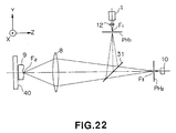
- Figure 22 illustrates the principle of a confocal optical system.
- light from a light source 1 is condensed by a lens 12 and then directed toward a half-mirror 31 via a pinhole PH1 located at a focal point F1 .
- the light from the light source 1 is transformed by the pinhole PH1 located at the focal point F1 into light equivalent to the a point source.
- Light reflected from the half-mirror 31 is condensed by a lens 8 and projected onto the surface of an object 9 . Shown here is a case in which the surface of the object 9 is in the focal position F2 of the lens 8 , and the object 9 is moved and scanned in the X-Y-Z direction by a three-dimensional moving stage 40 .
- Light scattered on the surface of the object 9 passes through the lens 8 , travels through the half-mirror 31 , and converges toward a point F3 conjugate with the focal position of the light source 1 .
- a pinhole PH2 is located in the position of this focal point F3 , and transmitted light is detected by a light sensor 10 .
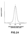
- the focal point F3 on the conjugate point side moves when the object surface Z0 is shifted to the front or back ( Z1 or Z2 ) of the focal position F2 , as shown in Figures 23a and 23b, and the output of the light sensor 10 is markedly reduced by the action of the pinhole.
- Figure 24 illustrates the relation between the position of the object surface and the output of the light sensor 10 .
- This structure makes it possible to shift the measurement object 9 by the three-dimensional moving stage 40 in the direction of the Z axis (in the direction of the optical axis) for each X-Y coordinate position, to sample the output of the light sensor 10 in the course of this displacement, and to designate the detected Z position corresponding to the maximum sampling output as the surface position of the object 9 . It is therefore possible to subject the measurement object 9 to three-dimensional measurements by sequentially changing the X-Y coordinate position and performing the same measurements.
- a disadvantage of this conventional apparatus is that each measurement instant yields information about a single point in space, making it necessary to spend much time to detect the surface shape.
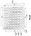
- the pinhole array PHA1 consists of pinholes arranged in a matrix.
- the light that has passed through the pinhole array PHA1 is transmitted through a half-mirror 31 , condensed by lenses 8a and 8b, and projected onto a measurement object 9 .
- the measurement object 9 is placed on top of a moving stage 35 capable of displacement in the direction of the Z axis.
- the light reflected by the measurement object 9 is condensed by the lenses 8a and 8b , reflected by the half-mirror 31 , and imaged at a position conjugate with the pinhole array PHA1 .
- a pinhole array PHA2 is located in the imaging position, and the light passing through the pinholes is detected by the individual light sensors 10 of a light sensor array.
- This conventional structure makes it possible to separately sample the outputs of the individual light sensors 10 of the light sensor array while displacing the moving stage 35 in the direction of the Z axis, and to designate the detected Z-direction position corresponding to the maximum output of the individual light sensors as the surface position of the object 9 .
- the moving stage 35 must be moved at a higher speed to further reduce the shape measurement time, but because the moving stage 35 must carry a measurement object, there is a limit to the high-speed movement. In other words, it is very difficult, for example, to use a high-speed moving stage to move a measurement object that is very heavy, a measurement object that has a very fine structure and thus cannot withstand the inertial force created by high-speed displacement, and the like.
- a prismatic device was usually used as the half-mirror 31 in Figure 25, and because this prismatic device requires a cubic space, the focal position of the light source (pinhole array PHA1 ) and the light-receiving. focal point (pinhole array PHA2 ) have to be located outside of the cubic space containing the half-mirror 31 , so it is impossible to make the distance between the lens 8a and each of the focal points smaller than the length of the cube of the half-mirror 31 .
- the focal point of the light source of a confocal unit and the light-receiving focal point are located with respect to the half-mirror 31 at geometric distances that vary with each confocal unit.
- the conventional mechanism illustrated in Figure 25 has limits as to the reductions in size and weight, and requires precise alignment between the focal point of the light source and the light-receiving focal point.
- An object of this invention which was devised in view of the foregoing, is to provide a confocal optical apparatus in which the size and weight can be reduced, which allows three-dimensional shape measurements to be performed rapidly and accurately, and in which the alignment of each portion is facilitated.
- a distinctive feature is that the first and second aperture portions are located in the same position and are conjointly used as identical aperture portions, and the detection surfaces of the light detectors are located substantially on the same surfaces as the conjointly used identical aperture portions.
- This invention involves conjointly using the first and second apertures as identical apertures and positioning the detection surfaces of the light detectors on substantially the same surfaces with these identical apertures, thereby making it possible to facilitate accurate alignment of the first and second apertures and the light detectors, and to render the structures of these portions thin, compact, and sturdy.
- a confocal optical apparatus comprises a light source, an optical element for receiving light from this light source and acting as a half-mirror and a diffraction grating, a first condensing device which is positioned in contact with or close to this optical element and which is designed for condensing zero-order light from the optical element, a pinhole for passing light condensed by this first condensing device, and a second condensing device for condensing the light that has passed through this pinhole and causing the light to converge toward a measurement object, and for causing the light scattered on the measurement object to converge toward the pinhole; in which the optical element directs toward the first condensing device the first-order diffracted light of the light reintroduced via the pinhole and the first condensing device; and which further comprises a light detector for receiving the first-order diffracted light condensed by the first condensing device.
- the structure of this invention is such that the light-receiving focal point and the focal point of the light source of the confocal optical system are in the same position, it is sufficient to form a common pinhole at the two focal points in this position, making it possible to obtain a stable confocal effect, dispensing with the alignment of the two focal points, and allowing the apparatus to be made small and lightweight.
- the confocal optical system can be accommodated within a very thin region because the arrangement is aimed at obtaining the effect of a half-mirror and a diffraction grating using a flat-plate hologram, a flat-plate, diffraction grate-type half-mirror, or some other optical element.
- a confocal optical apparatus comprises a parallel slit light generating device for generating parallel slit light undergoing sequential movable scanning, an aperture array in which a plurality of apertures for light passage are arranged in two dimensions and which is designed to direct the parallel slit light from the parallel light generating device, an optical element for receiving light that has passed through the aperture array and acting as a half-mirror and a diffraction grating, a lens array which is positioned close to this optical element and which is composed of a plurality of two-dimensionally arranged lenses for condensing zero-order light from the optical element, a pinhole array comprising a plurality of two-dimensionally arranged pinholes for passing light condensed by each of the lenses of the lens array, and a condensing device for condensing the light that has passed through each pinhole and projecting the light onto a measurement object, and for causing the light scattered on the measurement object to converge toward each pinhole; in which the optical element
- This invention involves directing parallel slit light toward a confocal optical system comprising two-dimensionally arranged apertures, lenses, pinholes, and light detectors, and receiving light reflected from a measurement object with the aid of the light detectors.
- the measurement object undergoes three-dimensional distance measurements based on the output of each light detector in accordance with the movable scanning of the parallel slit light and with the movable scanning of the movement control device.
- a confocal optical apparatus comprises a surface light ray generating device for generating surface light rays, an aperture array in which a plurality of apertures for light passage are arranged in two dimensions and which is designed to direct the surface light rays from the surface light ray generating device, an optical element for receiving light that has passed through the aperture array and acting as a half-mirror and a diffraction grating, a lens array positioned close to this optical element and comprising a plurality of two-dimensionally arranged lenses designed for condensing zero-order light from the optical element, a pinhole array comprising a plurality of two-dimensionally arranged pinholes for passing light condensed by each of the lenses of the lens array, and a condensing device for condensing the light that has passed through each pinhole and projecting the light onto a measurement object, and for causing the light scattered on the measurement object to converge toward each pinhole; in which the optical element directs toward the lens array the first
- This invention involves directing surface light rays toward a confocal optical system comprising two-dimensionally arranged apertures, lenses, pinholes, and light detectors, and receiving light reflected from a measurement object with the aid of the light detectors.
- the measurement object undergoes three-dimensional distance measurements based on the output of each light detector in accordance with movable scanning by the movement control device.
- the structure pertaining to this invention is thus aimed at obtaining results using pinholes that are in the same position as the light-receiving focal point and the light-source focal point of the confocal optical system, thus rendering the measuring device small, lightweight, and sturdy; adopting a structure in which all or part of the measurement device is movable results in rapid measurements, alignment, stability, measurement accuracy, and many other outstanding advantages.
- Figure 1 is a diagram illustrating a first embodiment of this invention.
- Figure 2 is a diagram illustrating this invention in principle.
- Figures 3a through 3c are diagrams illustrating the manner in which a hologram is exposed and the like.
- Figure 4 is a perspective cross section illustrating the structures of a hologram, lens array, light detector array, and other components.
- Figure 5 is a cross section illustrating the structures of a hologram, lens array, light detector array, and other components.
- Figures 6a through 6j are a flow chart illustrating an example of a manufacturing sequence for a light detector array and a pinhole array.
- Figures 7a through 7k are a flow chart illustrating another manufacturing sequence for a light detector array and a pinhole array.
- Figures 8a through 8j are a flow chart illustrating another manufacturing sequence for a light detector array and a pinhole array.
- Figure 9 is a diagram illustrating an example of a drive circuit for a light detector array.
- Figure 10 is a time chart showing each of the signals of the drive circuit.
- Figure 11 is a diagram illustrating a second embodiment of this invention.
- Figure 12 is a diagram illustrating a third embodiment of this invention.
- Figure 13 is a diagram illustrating a fourth embodiment of this invention.
- Figure 14 is a diagram illustrating the diffraction grating-type half-mirror used in the fourth embodiment.
- Figure 15 is a cross section illustrating other structures adopted for a hologram, lens array, light detector array, and other components.
- Figures 16a through 16m are a flow chart illustrating an example of a manufacturing sequence for the structure of Figure 15.
- Figure 17 is a cross section illustrating other structures adopted for a hologram, lens array, light detector array, and other components.
- Figure 18 is a cross section illustrating other structures adopted for a hologram, lens array, light detector array, and other components.
- Figures 19a and 19b are diagrams illustrating a fifth embodiment of this invention.
- Figure 20 is a diagram illustrating an example of another structure of a drive circuit for the light detector array.
- Figure 21 is a diagram illustrating an example of another structure of a drive circuit for the light detector array.
- Figure 22 is a diagram illustrating the principle of a confocal optical system.
- Figures 23a and 23b are diagrams illustrating the manner in which the focal point of a confocal optical system is shifted.
- Figure 24 is a diagram illustrating the output of a light sensor in relation to the distance between the object surface and the lens.
- Figure 25 is a diagram illustrating an example of a conventional three-dimensional shape measuring instrument using a confocal optical system.
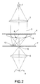
- FIG. 2 illustrates the basic structure of this invention.
- laser light (or monochromatic light based on the laser light) emitted from a light source 1 is transformed into parallel light 3 by a lens 2 and directed toward a reflection hologram 4 .
- the reflection hologram 4 which acts as a half-mirror and a diffraction grating, is exposed to the parallel light that forms an angle ⁇ with the direction of the optical axis, as shown in Figure 3a.
- parallel light which is shown by the solid lines in Figure 3b
- the hologram 4 developed, for example, to a diffraction efficiency of 40%
- the respective intensities of zero-order light (chain line) and first-order light (broken line) will be 60% and 40% of the incident light.
- the respective intensities of zero-order light and first-order light will be 60% and 40% of the incident light when, as shown in Figure 3c, this hologram is irradiated with parallel light opposite in direction to that shown in Figure 3b.
- the hologram 4 is irradiated with parallel light in the same direction as in Figure 3b, and the resulting zero-order light is made to converge toward the focal position 6 by a lens 5 adjacent to the reflection hologram 4 .
- a pinhole 7 is located in this focal position 6 , and light passes through the hole of the pinhole 7 .
- the light that has passed through the pinhole 7 is again condensed by a lens 8 and is directed toward a measurement object 9 .
- Light reflected from the measurement object 9 is again condensed by the lens 8 and again passed through the pinhole 7 .
- the light that has passed through the pinhole 7 is condensed by the lens 5 and is directed toward the hologram 4 assuming the form of parallel light opposite in direction to that of the parallel light 3 emitted from the light source.
- the first-order diffracted light of the parallel light incident on the hologram 4 is reflected at an angle ⁇ and condensed by the lens 5 .
- a light detector 10 is installed in this convergence position, and the luminous energy of the incident light is detected by the light detector 10 .
- the focal position on the light source side of the confocal optical system and the focal position on the light-receiving side are one and the same position 6 , and a common pinhole 7 can be used.
- a stable confocal effect can therefore be obtained, and the conventional alignment between the focal point of the light source and the light-receiving focal point becomes unnecessary.
- the reflection hologram 4 functions as a half-mirror makes it possible to implement the miniaturization (flattening) and weight reduction unattainable with conventional structures.
- Figure 1 illustrates a first embodiment of this invention
- the apparatus comprises a fixed portion 20 and a movable portion 30 that travels in the direction of the optical axis (Z direction).
- Laser light emitted from a laser light source 1 is transformed into slit parallel light by lenses 11 and 12 , and is deflected by a polyhedral rotating mirror 13 .
- the deflected slit parallel light is directed toward a telecentrically located cylindrical lens 2 , is deflected in the direction of the optical axis, and is sequentially scanned in the direction shown by the arrow A in the figure by the rotation of the polyhedral rotating mirror 13 .
- the polyhedral rotating mirror 13 is rotated and scanned by a movement controller 50 .
- Parallel slit light La scanned in the A direction is thus sequentially introduced from the fixed portion 20 into the movable portion 30 .
- An aperture array 14 in which apertures 14a for effectively directing light toward the individual lens 5a of a lens array 5 are formed at positions corresponding to the individual lenses is installed at the entrance pupil of the movable portion 30 , and a reflection hologram 4 acting as a half-mirror and diffraction grating is installed underneath.
- the reflection hologram 4 functions in the same manner as the holograms shown in Figures 2 and 3 above. The physical relationship between the upper and lower reflection hologram 4 and aperture array 14 may be reversed.
- the lens array 5 is positioned close to or in contact with the reflection hologram 4 underneath the reflection hologram 4 , and the zero-order light of the light incident on the hologram 4 is made to converge toward the focal position of each lens 5a .
- the pinholes 7a of a pinhole array 7 are located in the focal positions of the lenses 5a , and each of these condensed light rays passes through the pinholes 7a .
- the parallel slit light rays are made narrower than the pitch of the lenses 5a comprising the lens array 5 .
- Lenses 8a and 8b form a so-called telecentric system, and all the images of the pinhole array 7 are imaged in parallel in the direction of the optical axis. Therefore, the X-Y positions of the light spots imaged on a measurement object 9 do not change even when the movable portion 30 has been moved in the direction of the optical axis (Z axis).
- Light scattered on the measurement object 9 is condensed by the lenses 8b and 8a , passed through the pinhole array 7 having a confocal effect, directed toward the lens array 5 , and forced by the lenses 5a of the lens array 5 to strike the reflection hologram 4 in the direction coinciding with that shown in Figure 3c, assuming the form of parallel light opposite in direction to the slit parallel light exiting from the lens 2 .
- the first-order diffracted light rays of the reflection hologram 4 again strike the individual lenses 5a of the lens array 5 and converge at the respective angles ⁇ .
- a light detector array 10 is installed in such a way that individual light detectors 10a are located in each of these convergence positions.
- This structure involves fixedly installing a measurement object 9 on a suitable table 33 . Meanwhile, the movable portion 30 is moved by a movement controller 50 in the direction of the optical axis (Z axis) in synchronism with the rotational scanning performed by the polyhedral rotating mirror 13 .
- a three-dimensional measurement unit 60 sequentially samples the outputs of individual detectors 10a of the light detector array 10 during the movement of the movable portion 30 , and the Z position detected when each of the outputs reaches a maximum is designated as the position of the object surface.
- aperture array 14 In addition, the aperture array 14 , reflection hologram 4 , lens array 5 , light detector array 10 , and pinhole array 7 of this structure are formed into a flat assembly by a semiconductor process, as shown in Figures 4 and 5.
- the aperture array 14 in Figures 4 and 5 consists of a shielding plate, and apertures 14a are formed in this plate at positions corresponding to each of the lenses 5a .
- the shielding film of the aperture array 14 is formed, for example, by sputtering a three-layer Cr2O3/Cr/Cr2O3 film. Light reflected by the chromium contained in the intermediate layer of the three-layer film is subjected to multiple reflection and decay by the Cr2O3 film.
- a planar microlens may be used in this case as the lens array 5 .
- multiple lens 5a portions are fabricated by creating a refractive index distribution through the selective dispersion of ions within a flat glass substrate 5 .
- a nonreflective coating is applied to the light-admitting portion of each lens portion 5a of the lens array 5 .
- An exposed and developed hologram 4 is bonded along the section shown in Figure 3a to the glass substrate 5 of the lens array thus fabricated, and an aperture array 14 is then formed on top of this. If heat resistance is a problem during the manufacture of the hologram 4 , it is permissible to form the aperture array 14 on the glass substrate of the lens array 5 and then to bond the exposed and developed hologram 4 on top of this.
- a light detector array 10 and pinhole array 7 are formed at a pitch corresponding to the lens pitch of the lens array 5 on a planar glass substrate 15 in which a nonreflective coating is formed on the surface bonded to the glass substrate 5 .
- This portion is formed by aligning and bonding the planar glass substrate 15 (in which the light detector array 10 and pinhole array 7 have been formed) with the glass substrate 5 (in which the aperture array 14 , hologram 4 , and lens array 5 have been formed).
- the space between the two is filled with a transparent refractive liquid that has substantially the same refractive index as glass, making it possible to prevent irregular reflection from occurring at the interface between these substrates.
- the space between the two is filled with a transparent refractive liquid that has substantially the same refractive index as glass, making it possible to prevent irregular reflection from occurring at the interface between these substrates.
- FIGS. 6a through 6j illustrate the process for manufacturing the pinhole array 7 and light detector array 10 .
- the details of the process will now be described in accordance with the manufacturing sequence.
- Light detection elements comprising amorphous silicon 19 , transparent anode electrodes 17 , and metal cathode electrodes 22 are formed by this series of treatments, and pinhole shielding portions are formed from the nickel films 23 and 25 .
- FIGS 7a through 7k illustrate another manufacturing method. The details of this method will now be described in accordance with the manufacturing sequence.
- Light detection elements comprising amorphous silicon 19 , transparent anode electrodes 17 , and metal cathode electrodes 22 are formed by this series of treatments, and a pinhole shielding portion is formed from the nickel film 25 .
- FIGS 8a through 8j illustrate yet another manufacturing method. The details of this method will now be described in accordance with the manufacturing sequence.
- Light detection elements comprising amorphous silicon 19 , transparent anode electrodes 17 , and metal cathode electrodes 22 are formed by this series of treatments, and a pinhole shielding portion is formed from the nickel film 25 .
- this manufacturing method allows the pinhole portions of the nickel film 25 and amorphous silicon 19 to be removed simultaneously by the process (j) etching.
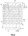
- Figure 9 illustrates a light detector array 10 composed of n ⁇ m light detectors S11 through Snm , and a circuit structure for reading the signals from these light detectors S11 through Snm .
- the light detectors in each row are connected to an analog multiplexer M1 by a common connecting line, and for even columns, the light detectors in each row are connected to an analog multiplexer M2 by a common line.
- the hatched light detectors E1 through Em are designed to generate read timing signals VD1 and VD2 for column units, and a light detector F is designed to output timing signals FD for starting a read scan cycle.
- the area inside the broken line in Figure 9 is irradiated at a certain point in time by the parallel slit light La in Figure 1, and the irradiated area is movably scanned in the direction of arrow A by performing a scanning procedure using a polyhedral rotating mirror.
- parallel slit light is alternately and movably scanned in the direction from the odd columns toward the even columns; signals detected by the light detectors of the odd columns are successively read by the multiplexer M1 for each row, and signals detected by the light detectors of the even columns are successively read by the multiplexer M2 for each row.
- This structure allows the two types of signals to be read independently for each column even when irradiation is performed using incident parallel slit light that covers both the odd and even columns. It is therefore possible to position light detectors close to each other, to reduce the surface area of the shielding portion of the aperture array 14 , and to miniaturize the structure of this portion.
- the hatched light detectors E1 through Em for generating timing signals are located in the matrix positions designated for the pinholes 7 at the ends of the light detector matrix, and are directly irradiated by the parallel slit light La from the fixed portion 20 .
- Signals VD1 are designed to determine the read timing of the odd columns
- signals VD2 are designed to determine the read timing of the even columns.
- a light detector F for generating read start timing signals FD is located, for example, in a matrix position designated for the pinhole 7 at the opposite end with respect to the light detector E1 of the first column.
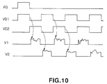
- Figure 10 illustrates the timing signals FD , VD1 , and VD2 , as well as the timing of the output signals V1 and V2 from the multiplexer M1 and M2 .
- the light detectors S11 through Smn function as a charge storage device, acting in such a way that the detector output of an odd column is read based on the fall of VD1 , and the detector output of an even column is read based on the fall of DV2 .
- This circuit structure therefore operates in such a way that while light is incident on the detectors of an odd column, the operation alternates between reading the detector output of an even column that contains an already stored charge and performing a reverse procedure.
- this circuit It is also possible with this circuit to read the detector output of an even column by delaying the signal VD1 and using this delayed signal as a trigger, and to read the detector output of an odd column by delaying the signal VD2 and using this delayed signal as a trigger. Another alternative is to delay the respective rises of the signals VD1 and VD2 , and to read the output of each detector with the aid of these delayed signals.
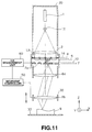
- Figure 11 illustrates another embodiment of this invention.
- parallel-plane light rays Lb of a nonscanning type are used instead of slit parallel light of the scanning type, as in the embodiment in Figure 1 above.
- the movable portion 30 consists of a lens 8a alone, and all the other parts are located in the fixed portion 20 .
- the other structures are the same as in the embodiment shown in Figure 1, and structural elements performing the same functions are assigned identical symbols.
- laser light emitted from a laser light source 1 is transformed into parallel-plane light rays Lb by cylindrical lenses 12 and 2 , and is directed toward an aperture array 14 .
- Light that has passed through the apertures of the aperture array 14 is caused to converge toward a measurement object 9 in the same manner as above via a hologram 4 , lens array 5 , a pinhole array 7 , and lenses 8a and 8b .
- Light scattered on the measurement object 9 passes through the lenses 8a and 8b , pinhole array 7 , and lens array 5 , strikes the hologram 4 , and enters the detectors of a light detector array 10 after being diffracted by the hologram 4 .
- this embodiment involves constructing the movable portion 30 from the lens 8b alone, the weight of moving parts can be reduced, and the structure for performing movable scanning can be simplified.
- the portion underneath the aperture array 14 may be constructed as a movable portion, as shown in Figure 1 above. It is also possible to configure all the structural elements (except for the measurement object 9 ) in Figure 11 in the form of a movable portion 30 .
- Figure 12 shows yet another embodiment of this invention.
- the entire apparatus is configured as a movable portion 30 in this case.
- a laser light source array 40 in which a plurality of laser elements are arranged in a matrix is used as the light source for generating surface light rays.
- This laser light source array is known as the array-type surface light generation semiconductor laser of Photonics Research Incorporated.
- a lens array 50 is used as the lens for converting into parallel light the light rays that are output by the array-type surface light generation semiconductor laser 40 .
- the other structures are the same as in the embodiment of Figure 1 or 11, and structural elements performing the same functions are assigned identical symbols.
- laser light emitted from the laser light source 40 is transformed into parallel-plane light rays by the lens array 50 , and is directed toward an aperture array 14 .
- Light that has passed through the apertures of the aperture array 14 is caused to converge toward a measurement object 9 in the same manner as above via a hologram 4 , lens array 5 , pinhole array 7 , and lenses 8a and 8b .
- Light scattered on the measurement object 9 passes through the lenses 8a and 8b , pinhole array 7 , and lens array 5 , strikes the hologram 4 , and enters the detectors of a light detector array 10 after being diffracted by the hologram 4 .
- This embodiment also allows the array-type surface light generation laser 40 to emit light sequentially in column units and to function as slit light, as in the embodiment illustrated in Figure 1 above.
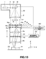
- Figure 13 illustrates still another embodiment of this invention.
- a diffraction grating-type half-mirror 41 such as that shown in Figure 14 is used instead of the reflection hologram 4 used in the aforementioned embodiments, and a quarter-wave plate 42 is interposed between the lenses 8a and 8b .
- the quarter-wave plate 42 in Figure 13 can be located in any position as long as it is in the optical path of the confocal optical system.
- the diffraction grating-type half-mirror 41 acts as a half-mirror and a diffraction grating in the same manner as the aforementioned reflection hologram 4 , and is described in Japanese Laid-Open Patent Application 61-17103.
- transparent members 43 and 44 of substantially the same refractive index are provided with a plurality of inclined surfaces, a polarization-dependent reflective film 45 is formed on these inclined surfaces, yielding a relief-type diffraction grating, and the assembly is supported by two parallel flat plates 46 and 47 on both sides.
- the reflective film 45 is configured in such a way that its transmittance is approximately 100% with respect to P polarized light and its reflectivity is approximately 100% with respect to S polarized light.
- a P polarized wave When, therefore, a P polarized wave is emitted from the light source 1 using a laser with linear polarization characteristics, the P polarized wave strikes the diffraction grating-type half-mirror 41 , and almost all the wave passes through. This P polarized wave then passes through the quarter-wave plate 42 , becomes circularly polarized light, and is caused to converge on the measurement object 9 by an object lens 8b .
- Light reflected from the measurement object 9 becomes an S polarized wave as a result of passing through the quarter-wave plate 42 , strikes the diffraction grating-type half-mirror 41 via a lens 8a and pinhole 7 , reflects from the reflective film 45 of the half-mirror 41 , and enters a light detector 10 .
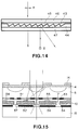
- Figure 15 illustrates a modified embodiment of the sheet-shape optical instrument portion shown in Figure 5 above.
- the microlens array 5 and light detector array 10 are bonded instead of the microlens array 5 and glass substrate 15 , as was the case in Figure 5 above.
- the function of the light detector array 10 and the function of the pinhole array 7 are performed with the aid of a structure comprising an upper shielding film 51 , a lower shielding film 52 , and upper insulating film 53 , a lower insulating film 54 , an upper electrode 55 , a lower electrode 56 , and a light detector portion 57 .
- These structural portions are bonded to the microlens array 5 by a refractive index adjusting solution 58 or the like.
- FIGs 16a through 16m illustrate the process for manufacturing the pinhole array 7 and light detector array 10 of the structure shown in Figure 15. The details of the process will now be described in accordance with the manufacturing sequence.
- Figure 17 illustrates an embodiment in which the light detector portion 57 is made not of amorphous silicon but of a single crystal silicon semiconductor, and the structural elements performing the same functions as in Figure 15 are assigned identical symbols.
- an SiO2 film is formed in this case on both surfaces of a silicon substrate using thermal oxidation or CVD, and a pn junction is formed by thermal diffusion or ion implantation using this SiO2 film as a mask, yielding a light detector array portion.
- an SiO2 film is again formed, patterning is performed, and a pinhole array is formed by RIE or other such etching technology.
- the light detector array having pinholes thus fabricated is then bonded to the microlens array 5 with the aid of a refractive index adjusting solution 58 .
- Silicon and a microlens array may also be directly joined using a lamination SOI technique during bonding with the microlens.
- the upper electrode 55 and the lower electrode 56 may be sandwiched, as in the embodiment shown in Figure 15 or 17, or they may be formed within the same plane, as shown in Figure 18.
- Figure 19a illustrates yet another modified example of the sheet-shape optical instrument portion shown in Figure 5 or 15;
- Figure 19b is a plan view of an annular light detector 10a .
- Figures 19a and 19b show a case in which the function of the half-mirror can be performed by a half-mirror coating film 59 and in which light reflected by the half-mirror film 59 can be detected by making the light detector array 10 annular in shape.
- the annular light detector 10 and the pinhole array 7 are formed on the glass substrate 15 by a semiconductor process.
- FIG 20 illustrates a modified embodiment of a circuit structure for reading the signals of each of the detectors of the light detector array 10 shown in Figure 9 above.
- each of the detectors is divided into four blocks.
- light detectors in the (4n - 3) column are connected to an analog multiplexer M1 ; light detectors in the (4n - 2) column, to an analog multiplexer M2 ; light detectors in the (4n - 1) column, to an analog multiplexer M3 ; and light detectors in the 4n column, to an analog multiplexer M4 .
- the number of divisions is increased in comparison with the previous embodiment involving division into two parts, making it possible to increase the speed at which signals are read.
- the analog multiplexers may be connected to the light detector array by wire bonding or the like, or they may be made into a monolith together with the light detector array inside the same substrate. It is also possible to divide the assembly into a plurality of blocks not only in the column direction but also in the row direction.
- Figure 21 illustrates a circuit for reading signals from a light detector array irradiated with surface light rays, as shown in Figure 11 or 12. It is possible in this case to adopt an X-Y address system in which transistors and other switching elements are incorporated into the light detector array. A charge transfer system may be adopted for the read mode.
- the measurement object 9 was fixed in the embodiments shown in Figures 1, 11, and 12, although it is also possible to adopt a movable structure in which the measurement object 9 is placed on an X-Y moving stage, and measurements are conducted by suitably varying the measurement object field.
- higher-resolution measurements can be performed by adopting a structure in which this X-Y moving stage or movable portion 30 can be microscopically displaced in the X-Y direction.
- inventions shown in Figures 1, 11, and 12 also allow all the measurement instruments to be fixed and three-dimensional measurements to be performed by movably scanning the measurement object 9 in three-dimensional directions.
- This invention can be used as a three-dimensional measurement apparatus for measuring the shape of a measurement object in three dimensions.
Abstract
Description
- This invention relates to a three-dimensional shape measuring apparatus in which a confocal optical system is employed, and in particular relates to a confocal optical apparatus for performing three-dimensional measurements using a hologram or a diffraction grating-type half-mirror.
- So-called confocal optical systems are apparatus for measuring distances. Figure 22 illustrates the principle of a confocal optical system.
- In Figure 22, light from a
light source 1 is condensed by alens 12 and then directed toward a half-mirror 31 via a pinhole PH1 located at a focal point F1. The light from thelight source 1 is transformed by the pinhole PH1 located at the focal point F1 into light equivalent to the a point source. Light reflected from the half-mirror 31 is condensed by alens 8 and projected onto the surface of anobject 9. Shown here is a case in which the surface of theobject 9 is in the focal position F2 of thelens 8, and theobject 9 is moved and scanned in the X-Y-Z direction by a three-dimensional movingstage 40. Light scattered on the surface of theobject 9 passes through thelens 8, travels through the half-mirror 31, and converges toward a point F3 conjugate with the focal position of thelight source 1. A pinhole PH2 is located in the position of this focal point F3, and transmitted light is detected by alight sensor 10. - With this structure, the focal point F3 on the conjugate point side moves when the object surface Z0 is shifted to the front or back (Z1 or Z2) of the focal position F2, as shown in Figures 23a and 23b, and the output of the
light sensor 10 is markedly reduced by the action of the pinhole. Figure 24 illustrates the relation between the position of the object surface and the output of thelight sensor 10. - This structure makes it possible to shift the
measurement object 9 by the three-dimensional movingstage 40 in the direction of the Z axis (in the direction of the optical axis) for each X-Y coordinate position, to sample the output of thelight sensor 10 in the course of this displacement, and to designate the detected Z position corresponding to the maximum sampling output as the surface position of theobject 9. It is therefore possible to subject themeasurement object 9 to three-dimensional measurements by sequentially changing the X-Y coordinate position and performing the same measurements. - A disadvantage of this conventional apparatus, however, is that each measurement instant yields information about a single point in space, making it necessary to spend much time to detect the surface shape.
- In view of this, an attempt was made in Japanese Laid-Open Patent Application 4-265918 to arrange the confocal optical system in two dimensions and to detect each object position in parallel; the corresponding structure is illustrated in Figure 25.
- Specifically, with the apparatus illustrated in Figure 25 above, light from a
light source 1 passes throughlenses mirror 31, condensed bylenses measurement object 9. Themeasurement object 9 is placed on top of a movingstage 35 capable of displacement in the direction of the Z axis. The light reflected by themeasurement object 9 is condensed by thelenses mirror 31, and imaged at a position conjugate with the pinhole array PHA1. A pinhole array PHA2 is located in the imaging position, and the light passing through the pinholes is detected by theindividual light sensors 10 of a light sensor array. - This conventional structure makes it possible to separately sample the outputs of the
individual light sensors 10 of the light sensor array while displacing themoving stage 35 in the direction of the Z axis, and to designate the detected Z-direction position corresponding to the maximum output of the individual light sensors as the surface position of theobject 9. - Because this conventional technique dispenses with the need to move the moving stage in the XY direction, the measuring time can be reduced in comparison with the conventional mechanism illustrated in Figure 22 above.
- Even with the apparatus illustrated in Figure 25, the moving
stage 35 must be moved at a higher speed to further reduce the shape measurement time, but because the movingstage 35 must carry a measurement object, there is a limit to the high-speed movement. In other words, it is very difficult, for example, to use a high-speed moving stage to move a measurement object that is very heavy, a measurement object that has a very fine structure and thus cannot withstand the inertial force created by high-speed displacement, and the like. - Fixing the
measurement object 9 and moving and displacing the measuring instrument itself in the Z direction was suggested as a way of overcoming this shortcoming. To be able to be displaced at a high speed, however, the measuring instrument itself must be small and lightweight, have a sturdy structure, and withstand the inertial force created by high-speed displacement. With the conventional technique illustrated in Figure 25, however, no measures related to high-speed movement have been adopted, thus making it likely that the confocal optical system will break or that other undesirable phenomena will occur during high-speed movement. In particular, it is important for a confocal optical system that the pinhole arrays PHA1 and PHA2 always remain in exact conjugate positions with respect to the half-mirror 31 so that the confocal optical system is always effective, but in the past there has been a limit to reconciling this requirement with a need for a reduction in size and weight. - In addition, a prismatic device was usually used as the half-
mirror 31 in Figure 25, and because this prismatic device requires a cubic space, the focal position of the light source (pinhole array PHA1) and the light-receiving. focal point (pinhole array PHA2) have to be located outside of the cubic space containing the half-mirror 31, so it is impossible to make the distance between thelens 8a and each of the focal points smaller than the length of the cube of the half-mirror 31. In addition, the focal point of the light source of a confocal unit and the light-receiving focal point are located with respect to the half-mirror 31 at geometric distances that vary with each confocal unit. Thus, the conventional mechanism illustrated in Figure 25 has limits as to the reductions in size and weight, and requires precise alignment between the focal point of the light source and the light-receiving focal point. - An object of this invention, which was devised in view of the foregoing, is to provide a confocal optical apparatus in which the size and weight can be reduced, which allows three-dimensional shape measurements to be performed rapidly and accurately, and in which the alignment of each portion is facilitated.
- According to this invention, in a confocal optical apparatus comprising a light source, a first aperture portion for passing light emitted from this light source and obtaining a point source, an objective lens for causing the light that has passed through this first aperture portion to converge on a measurement object, a second aperture portion located on a plane conjugate with the convergence surface on this measurement object, and light detectors for detecting light that has passed through the second aperture portion, a distinctive feature is that the first and second aperture portions are located in the same position and are conjointly used as identical aperture portions, and the detection surfaces of the light detectors are located substantially on the same surfaces as the conjointly used identical aperture portions.
- This invention involves conjointly using the first and second apertures as identical apertures and positioning the detection surfaces of the light detectors on substantially the same surfaces with these identical apertures, thereby making it possible to facilitate accurate alignment of the first and second apertures and the light detectors, and to render the structures of these portions thin, compact, and sturdy.
- In addition, according to this invention, a confocal optical apparatus comprises a light source, an optical element for receiving light from this light source and acting as a half-mirror and a diffraction grating, a first condensing device which is positioned in contact with or close to this optical element and which is designed for condensing zero-order light from the optical element, a pinhole for passing light condensed by this first condensing device, and a second condensing device for condensing the light that has passed through this pinhole and causing the light to converge toward a measurement object, and for causing the light scattered on the measurement object to converge toward the pinhole; in which the optical element directs toward the first condensing device the first-order diffracted light of the light reintroduced via the pinhole and the first condensing device; and which further comprises a light detector for receiving the first-order diffracted light condensed by the first condensing device.
- Specifically, since the structure of this invention is such that the light-receiving focal point and the focal point of the light source of the confocal optical system are in the same position, it is sufficient to form a common pinhole at the two focal points in this position, making it possible to obtain a stable confocal effect, dispensing with the alignment of the two focal points, and allowing the apparatus to be made small and lightweight. In addition, the confocal optical system can be accommodated within a very thin region because the arrangement is aimed at obtaining the effect of a half-mirror and a diffraction grating using a flat-plate hologram, a flat-plate, diffraction grate-type half-mirror, or some other optical element.
- Furthermore, according to this invention, a confocal optical apparatus comprises a parallel slit light generating device for generating parallel slit light undergoing sequential movable scanning, an aperture array in which a plurality of apertures for light passage are arranged in two dimensions and which is designed to direct the parallel slit light from the parallel light generating device, an optical element for receiving light that has passed through the aperture array and acting as a half-mirror and a diffraction grating, a lens array which is positioned close to this optical element and which is composed of a plurality of two-dimensionally arranged lenses for condensing zero-order light from the optical element, a pinhole array comprising a plurality of two-dimensionally arranged pinholes for passing light condensed by each of the lenses of the lens array, and a condensing device for condensing the light that has passed through each pinhole and projecting the light onto a measurement object, and for causing the light scattered on the measurement object to converge toward each pinhole; in which the optical element directs toward the lens array the first-order diffracted light of the light reintroduced via each of the pinholes and the lens array; and which further comprises a light detector array comprising a plurality of two-dimensionally arranged light detectors for receiving the first-order diffracted light condensed by each of the lenses of the lens array, a movement control device for moving in the direction of the optical axis at least some of the parallel slit light generating device, aperture array, optical element, lens array, pinhole array, condensing device, and light detector array, and a three-dimensional distance measuring device for measuring the measurement object in three dimensions based on the output of each light detector in accordance with the movable scanning of the parallel slit light and with the movement control of the movement control device.
- This invention involves directing parallel slit light toward a confocal optical system comprising two-dimensionally arranged apertures, lenses, pinholes, and light detectors, and receiving light reflected from a measurement object with the aid of the light detectors. The measurement object undergoes three-dimensional distance measurements based on the output of each light detector in accordance with the movable scanning of the parallel slit light and with the movable scanning of the movement control device.
- Moreover, according to this invention, a confocal optical apparatus comprises a surface light ray generating device for generating surface light rays, an aperture array in which a plurality of apertures for light passage are arranged in two dimensions and which is designed to direct the surface light rays from the surface light ray generating device, an optical element for receiving light that has passed through the aperture array and acting as a half-mirror and a diffraction grating, a lens array positioned close to this optical element and comprising a plurality of two-dimensionally arranged lenses designed for condensing zero-order light from the optical element, a pinhole array comprising a plurality of two-dimensionally arranged pinholes for passing light condensed by each of the lenses of the lens array, and a condensing device for condensing the light that has passed through each pinhole and projecting the light onto a measurement object, and for causing the light scattered on the measurement object to converge toward each pinhole; in which the optical element directs toward the lens array the first-order diffracted light of the light reintroduced via each of the pinholes and the lens array; and which further comprises a light detector array comprising a plurality of two-dimensionally arranged light detectors for receiving the first-order diffracted light condensed by each of the lenses of the lens array, a movement control device for moving in the direction of the optical axis at least some of the surface light ray generating device, aperture array, optical element, lens array, pinhole array, condensing device, and light detector array, and a three-dimensional distance measuring device for measuring the measurement object in three dimensions based on the output of each light detector in accordance with the movement control of the movement control device.
- This invention involves directing surface light rays toward a confocal optical system comprising two-dimensionally arranged apertures, lenses, pinholes, and light detectors, and receiving light reflected from a measurement object with the aid of the light detectors. The measurement object undergoes three-dimensional distance measurements based on the output of each light detector in accordance with movable scanning by the movement control device.
- The structure pertaining to this invention is thus aimed at obtaining results using pinholes that are in the same position as the light-receiving focal point and the light-source focal point of the confocal optical system, thus rendering the measuring device small, lightweight, and sturdy; adopting a structure in which all or part of the measurement device is movable results in rapid measurements, alignment, stability, measurement accuracy, and many other outstanding advantages.
- Figure 1 is a diagram illustrating a first embodiment of this invention.
- Figure 2 is a diagram illustrating this invention in principle.
- Figures 3a through 3c are diagrams illustrating the manner in which a hologram is exposed and the like.
- Figure 4 is a perspective cross section illustrating the structures of a hologram, lens array, light detector array, and other components.
- Figure 5 is a cross section illustrating the structures of a hologram, lens array, light detector array, and other components.
- Figures 6a through 6j are a flow chart illustrating an example of a manufacturing sequence for a light detector array and a pinhole array.
- Figures 7a through 7k are a flow chart illustrating another manufacturing sequence for a light detector array and a pinhole array.
- Figures 8a through 8j are a flow chart illustrating another manufacturing sequence for a light detector array and a pinhole array.
- Figure 9 is a diagram illustrating an example of a drive circuit for a light detector array.
- Figure 10 is a time chart showing each of the signals of the drive circuit.
- Figure 11 is a diagram illustrating a second embodiment of this invention.
- Figure 12 is a diagram illustrating a third embodiment of this invention.
- Figure 13 is a diagram illustrating a fourth embodiment of this invention.
- Figure 14 is a diagram illustrating the diffraction grating-type half-mirror used in the fourth embodiment.
- Figure 15 is a cross section illustrating other structures adopted for a hologram, lens array, light detector array, and other components.
- Figures 16a through 16m are a flow chart illustrating an example of a manufacturing sequence for the structure of Figure 15.
- Figure 17 is a cross section illustrating other structures adopted for a hologram, lens array, light detector array, and other components.
- Figure 18 is a cross section illustrating other structures adopted for a hologram, lens array, light detector array, and other components.
- Figures 19a and 19b are diagrams illustrating a fifth embodiment of this invention.
- Figure 20 is a diagram illustrating an example of another structure of a drive circuit for the light detector array.
- Figure 21 is a diagram illustrating an example of another structure of a drive circuit for the light detector array.
- Figure 22 is a diagram illustrating the principle of a confocal optical system.
- Figures 23a and 23b are diagrams illustrating the manner in which the focal point of a confocal optical system is shifted.
- Figure 24 is a diagram illustrating the output of a light sensor in relation to the distance between the object surface and the lens.
- Figure 25 is a diagram illustrating an example of a conventional three-dimensional shape measuring instrument using a confocal optical system.
- This invention will now be described in detail through the embodiments shown in the accompanying drawings.
- Figure 2 illustrates the basic structure of this invention.
- In Figure 2, laser light (or monochromatic light based on the laser light) emitted from a
light source 1 is transformed intoparallel light 3 by alens 2 and directed toward areflection hologram 4. Thereflection hologram 4, which acts as a half-mirror and a diffraction grating, is exposed to the parallel light that forms an angle Φ with the direction of the optical axis, as shown in Figure 3a. When parallel light, which is shown by the solid lines in Figure 3b, is incident on thehologram 4 developed, for example, to a diffraction efficiency of 40%, the respective intensities of zero-order light (chain line) and first-order light (broken line) will be 60% and 40% of the incident light. In addition, the respective intensities of zero-order light and first-order light will be 60% and 40% of the incident light when, as shown in Figure 3c, this hologram is irradiated with parallel light opposite in direction to that shown in Figure 3b. - In Figure 2, the
hologram 4 is irradiated with parallel light in the same direction as in Figure 3b, and the resulting zero-order light is made to converge toward thefocal position 6 by alens 5 adjacent to thereflection hologram 4. Apinhole 7 is located in thisfocal position 6, and light passes through the hole of thepinhole 7. The light that has passed through thepinhole 7 is again condensed by alens 8 and is directed toward ameasurement object 9. Light reflected from themeasurement object 9 is again condensed by thelens 8 and again passed through thepinhole 7. The light that has passed through thepinhole 7 is condensed by thelens 5 and is directed toward thehologram 4 assuming the form of parallel light opposite in direction to that of theparallel light 3 emitted from the light source. As shown in Figure 3c, the first-order diffracted light of the parallel light incident on thehologram 4 is reflected at an angle Φ and condensed by thelens 5. Alight detector 10 is installed in this convergence position, and the luminous energy of the incident light is detected by thelight detector 10. - Specifically, with this system, the focal position on the light source side of the confocal optical system and the focal position on the light-receiving side are one and the
same position 6, and acommon pinhole 7 can be used. A stable confocal effect can therefore be obtained, and the conventional alignment between the focal point of the light source and the light-receiving focal point becomes unnecessary. In addition, the fact that thereflection hologram 4 functions as a half-mirror makes it possible to implement the miniaturization (flattening) and weight reduction unattainable with conventional structures. - Figure 1 illustrates a first embodiment of this invention; the apparatus comprises a fixed
portion 20 and amovable portion 30 that travels in the direction of the optical axis (Z direction). - Laser light emitted from a
laser light source 1 is transformed into slit parallel light bylenses rotating mirror 13. The deflected slit parallel light is directed toward a telecentrically locatedcylindrical lens 2, is deflected in the direction of the optical axis, and is sequentially scanned in the direction shown by the arrow A in the figure by the rotation of the polyhedralrotating mirror 13. The polyhedralrotating mirror 13 is rotated and scanned by amovement controller 50. Parallel slit light La scanned in the A direction is thus sequentially introduced from the fixedportion 20 into themovable portion 30. - It is also possible to use a galvano-mirror instead of the polyhedral
rotating mirror 13, as it is to perform uniform scanning using an f-ϑ lens instead of thecylindrical lens 2. - An
aperture array 14 in whichapertures 14a for effectively directing light toward theindividual lens 5a of alens array 5 are formed at positions corresponding to the individual lenses is installed at the entrance pupil of themovable portion 30, and areflection hologram 4 acting as a half-mirror and diffraction grating is installed underneath. Thereflection hologram 4 functions in the same manner as the holograms shown in Figures 2 and 3 above. The physical relationship between the upper andlower reflection hologram 4 andaperture array 14 may be reversed. - The
lens array 5 is positioned close to or in contact with thereflection hologram 4 underneath thereflection hologram 4, and the zero-order light of the light incident on thehologram 4 is made to converge toward the focal position of eachlens 5a. Thepinholes 7a of apinhole array 7 are located in the focal positions of thelenses 5a, and each of these condensed light rays passes through thepinholes 7a. The parallel slit light rays are made narrower than the pitch of thelenses 5a comprising thelens array 5. -
Lenses pinhole array 7 are imaged in parallel in the direction of the optical axis. Therefore, the X-Y positions of the light spots imaged on ameasurement object 9 do not change even when themovable portion 30 has been moved in the direction of the optical axis (Z axis). - Light scattered on the
measurement object 9 is condensed by thelenses pinhole array 7 having a confocal effect, directed toward thelens array 5, and forced by thelenses 5a of thelens array 5 to strike thereflection hologram 4 in the direction coinciding with that shown in Figure 3c, assuming the form of parallel light opposite in direction to the slit parallel light exiting from thelens 2. The first-order diffracted light rays of thereflection hologram 4 again strike theindividual lenses 5a of thelens array 5 and converge at the respective angles Φ. Alight detector array 10 is installed in such a way that individuallight detectors 10a are located in each of these convergence positions. - This structure involves fixedly installing a
measurement object 9 on a suitable table 33. Meanwhile, themovable portion 30 is moved by amovement controller 50 in the direction of the optical axis (Z axis) in synchronism with the rotational scanning performed by the polyhedralrotating mirror 13. A three-dimensional measurement unit 60 sequentially samples the outputs ofindividual detectors 10a of thelight detector array 10 during the movement of themovable portion 30, and the Z position detected when each of the outputs reaches a maximum is designated as the position of the object surface. - In addition, the
aperture array 14,reflection hologram 4,lens array 5,light detector array 10, andpinhole array 7 of this structure are formed into a flat assembly by a semiconductor process, as shown in Figures 4 and 5. - Specifically, the
aperture array 14 in Figures 4 and 5 consists of a shielding plate, andapertures 14a are formed in this plate at positions corresponding to each of thelenses 5a. The shielding film of theaperture array 14 is formed, for example, by sputtering a three-layer Cr₂O₃/Cr/Cr₂O₃ film. Light reflected by the chromium contained in the intermediate layer of the three-layer film is subjected to multiple reflection and decay by the Cr₂O₃ film. - A planar microlens (PML) may be used in this case as the
lens array 5. With a planar microlens,multiple lens 5a portions are fabricated by creating a refractive index distribution through the selective dispersion of ions within aflat glass substrate 5. A nonreflective coating is applied to the light-admitting portion of eachlens portion 5a of thelens array 5. - An exposed and developed
hologram 4 is bonded along the section shown in Figure 3a to theglass substrate 5 of the lens array thus fabricated, and anaperture array 14 is then formed on top of this. If heat resistance is a problem during the manufacture of thehologram 4, it is permissible to form theaperture array 14 on the glass substrate of thelens array 5 and then to bond the exposed and developedhologram 4 on top of this. - In addition, a
light detector array 10 andpinhole array 7 are formed at a pitch corresponding to the lens pitch of thelens array 5 on aplanar glass substrate 15 in which a nonreflective coating is formed on the surface bonded to theglass substrate 5. - This portion is formed by aligning and bonding the planar glass substrate 15 (in which the
light detector array 10 andpinhole array 7 have been formed) with the glass substrate 5 (in which theaperture array 14,hologram 4, andlens array 5 have been formed). - When the
microlens substrate 5 and theglass sensor substrate 15 are bonded, the space between the two is filled with a transparent refractive liquid that has substantially the same refractive index as glass, making it possible to prevent irregular reflection from occurring at the interface between these substrates. - Similarly, when the
microlens substrate 5 and thehologram 4 are bonded, the space between the two is filled with a transparent refractive liquid that has substantially the same refractive index as glass, making it possible to prevent irregular reflection from occurring at the interface between these substrates. - Figures 6a through 6j illustrate the process for manufacturing the
pinhole array 7 andlight detector array 10. The details of the process will now be described in accordance with the manufacturing sequence. - (a)
Planar glass substrate 15 - (b) A transparent conductive film (TCO) 16 is formed on the
planar glass substrate 15. SnO₂ or the like is used for the TCO. - (c) Except for the light
detector element portions 17 andpinhole portions 18, everything is removed from the transparentconductive film 16 by, for example, etching or the like. The purpose of retaining the transparent conductive film of the pinhole portions in this process is to prevent the glass of the aperture portions of the pinholes from being abraded by the etching of the subsequent process (g). - (d)
Amorphous silicon 19 is formed on top of this. - (e) The
pinhole portions 18 of theamorphous silicon 19 are removed using etching or the like. - (f) A
nickel film 21 is formed. - (g) Except for the light
detector element portions 17 andpinhole portions 18, everything is removed from thenickel film 21 by, for example, etching or the like. Each pinhole aperture is also formed by etching. - (h) A transparent insulating
film 24 is formed on this overcoat. - (i) A
nickel film 25 is then formed. - (j) The
pinhole portions 26 of thenickel film 25 are formed by etching. - Light detection elements comprising
amorphous silicon 19,transparent anode electrodes 17, andmetal cathode electrodes 22 are formed by this series of treatments, and pinhole shielding portions are formed from thenickel films - Figures 7a through 7k illustrate another manufacturing method. The details of this method will now be described in accordance with the manufacturing sequence.
- (a)
Planar glass substrate 15 - (b) A transparent conductive film (TCO) 16 is formed on the
planar glass substrate 15. - (c) Except for the light
detector element portions 17 andpinhole portions 18, everything is removed from the transparentconductive film 16 by, for example, etching or the like. The purpose of retaining the transparent conductive film of the pinhole portions in this process is to prevent the glass of the aperture portions of the pinholes from being abraded by the etching of the subsequent processes (e) and (k). - (d)
Amorphous silicon 19 is formed on top of this. - (e) The
pinhole portions 18 of theamorphous silicon 19 are removed using etching or the like. - (f) A
nickel film 21 is formed. - (g) Except for the light
detector element portions 22, everything is removed from thenickel film 21 by, for example, etching or the like. - (h) An insulating
film 24 is formed on this overcoat. - (i) The insulating
film 24,amorphous silicon 19, andpinhole portions 27 are removed by etching or the like. - (j) A
nickel film 25 is then formed. - (k) The pinhole 26 portions of the
nickel film 25 are removed by etching to form pinholes. - Light detection elements comprising
amorphous silicon 19,transparent anode electrodes 17, andmetal cathode electrodes 22 are formed by this series of treatments, and a pinhole shielding portion is formed from thenickel film 25. - Figures 8a through 8j illustrate yet another manufacturing method. The details of this method will now be described in accordance with the manufacturing sequence.
- (a)
Planar glass substrate 15 - (b) A transparent conductive film (TCO) 16 is formed on the
planar glass substrate 15. - (c) Except for the light
detector element portions 17 andpinhole portions 18, everything is removed from the transparentconductive film 16 by, for example, etching or the like. The purpose of retaining the transparent conductive film of the pinhole portions in this process is to prevent the glass of the aperture portions of the pinholes from being abraded by the etching of the subsequent process (j). - (d)
Amorphous silicon 19 is formed on top of this. - (e) A
nickel film 21 is formed. - (f) Except for the light
detector element portions 22, everything is removed from thenickel film 21 by, for example, etching or the like. - (g) An insulating
film 24 is formed on this overcoat. - (h) The
pinhole portions 27 are removed from the insulatingfilm 24 by etching or the like. - (i) A
nickel film 25 is then formed. - (j) The
pinhole portions 28 of thenickel film 25 andamorphous silicon 19 are removed by etching to form pinholes. - Light detection elements comprising
amorphous silicon 19,transparent anode electrodes 17, andmetal cathode electrodes 22 are formed by this series of treatments, and a pinhole shielding portion is formed from thenickel film 25. Specifically, this manufacturing method allows the pinhole portions of thenickel film 25 andamorphous silicon 19 to be removed simultaneously by the process (j) etching. - Figure 9 illustrates a
light detector array 10 composed of n À m light detectors S11 through Snm, and a circuit structure for reading the signals from these light detectors S11 through Snm. For odd columns, the light detectors in each row are connected to an analog multiplexer M1 by a common connecting line, and for even columns, the light detectors in each row are connected to an analog multiplexer M2 by a common line. The hatched light detectors E1 through Em are designed to generate read timing signals VD1 and VD2 for column units, and a light detector F is designed to output timing signals FD for starting a read scan cycle. - The area inside the broken line in Figure 9 is irradiated at a certain point in time by the parallel slit light La in Figure 1, and the irradiated area is movably scanned in the direction of arrow A by performing a scanning procedure using a polyhedral rotating mirror. Specifically, parallel slit light is alternately and movably scanned in the direction from the odd columns toward the even columns; signals detected by the light detectors of the odd columns are successively read by the multiplexer M1 for each row, and signals detected by the light detectors of the even columns are successively read by the multiplexer M2 for each row.
- This structure allows the two types of signals to be read independently for each column even when irradiation is performed using incident parallel slit light that covers both the odd and even columns. It is therefore possible to position light detectors close to each other, to reduce the surface area of the shielding portion of the
aperture array 14, and to miniaturize the structure of this portion. - In Figure 9, the hatched light detectors E1 through Em for generating timing signals are located in the matrix positions designated for the
pinholes 7 at the ends of the light detector matrix, and are directly irradiated by the parallel slit light La from the fixedportion 20. Signals VD1 are designed to determine the read timing of the odd columns, and signals VD2 are designed to determine the read timing of the even columns. In addition, a light detector F for generating read start timing signals FD is located, for example, in a matrix position designated for thepinhole 7 at the opposite end with respect to the light detector E1 of the first column. - Figure 10 illustrates the timing signals FD, VD1, and VD2, as well as the timing of the output signals V1 and V2 from the multiplexer M1 and M2. In this case, the light detectors S11 through Smn function as a charge storage device, acting in such a way that the detector output of an odd column is read based on the fall of VD1, and the detector output of an even column is read based on the fall of DV2. This circuit structure therefore operates in such a way that while light is incident on the detectors of an odd column, the operation alternates between reading the detector output of an even column that contains an already stored charge and performing a reverse procedure.
- It is also possible to use a charge transfer method in which CCD camera sensors are used instead of the multiplexes M1 and M2.
- It is also possible with this circuit to read the detector output of an even column by delaying the signal VD1 and using this delayed signal as a trigger, and to read the detector output of an odd column by delaying the signal VD2 and using this delayed signal as a trigger. Another alternative is to delay the respective rises of the signals VD1 and VD2, and to read the output of each detector with the aid of these delayed signals.
- Figure 11 illustrates another embodiment of this invention. In this case, parallel-plane light rays Lb of a nonscanning type are used instead of slit parallel light of the scanning type, as in the embodiment in Figure 1 above. In addition, the
movable portion 30 consists of alens 8a alone, and all the other parts are located in the fixedportion 20. The other structures are the same as in the embodiment shown in Figure 1, and structural elements performing the same functions are assigned identical symbols. - Specifically, laser light emitted from a
laser light source 1 is transformed into parallel-plane light rays Lb bycylindrical lenses aperture array 14. Light that has passed through the apertures of theaperture array 14 is caused to converge toward ameasurement object 9 in the same manner as above via ahologram 4,lens array 5, apinhole array 7, andlenses measurement object 9 passes through thelenses pinhole array 7, andlens array 5, strikes thehologram 4, and enters the detectors of alight detector array 10 after being diffracted by thehologram 4. - Because parallel-plane light rays Lb are used in this case, the return light of the parallel-plane light rays Lb enters all the detectors of the
light detector array 10 simultaneously. - Since this embodiment involves constructing the
movable portion 30 from thelens 8b alone, the weight of moving parts can be reduced, and the structure for performing movable scanning can be simplified. - Even when parallel-plane light rays Lb are used in the manner shown in Figure 11, the portion underneath the aperture array 14 (
aperture array 14,hologram 4,lens array 5,light detector array 10,pinhole array 7, andlenses movable portion 30. - Figure 12 shows yet another embodiment of this invention. The entire apparatus is configured as a
movable portion 30 in this case. In addition, a laserlight source array 40 in which a plurality of laser elements are arranged in a matrix is used as the light source for generating surface light rays. This laser light source array is known as the array-type surface light generation semiconductor laser of Photonics Research Incorporated. In addition, alens array 50 is used as the lens for converting into parallel light the light rays that are output by the array-type surface lightgeneration semiconductor laser 40. The other structures are the same as in the embodiment of Figure 1 or 11, and structural elements performing the same functions are assigned identical symbols. - Specifically, in Figure 12, laser light emitted from the
laser light source 40 is transformed into parallel-plane light rays by thelens array 50, and is directed toward anaperture array 14. Light that has passed through the apertures of theaperture array 14 is caused to converge toward ameasurement object 9 in the same manner as above via ahologram 4,lens array 5,pinhole array 7, andlenses measurement object 9 passes through thelenses pinhole array 7, andlens array 5, strikes thehologram 4, and enters the detectors of alight detector array 10 after being diffracted by thehologram 4. - This embodiment also allows the array-type surface
light generation laser 40 to emit light sequentially in column units and to function as slit light, as in the embodiment illustrated in Figure 1 above. - Figure 13 illustrates still another embodiment of this invention. In this embodiment, a diffraction grating-type half-
mirror 41 such as that shown in Figure 14 is used instead of thereflection hologram 4 used in the aforementioned embodiments, and a quarter-wave plate 42 is interposed between thelenses wave plate 42 in Figure 13 can be located in any position as long as it is in the optical path of the confocal optical system. - The diffraction grating-type half-
mirror 41 acts as a half-mirror and a diffraction grating in the same manner as theaforementioned reflection hologram 4, and is described in Japanese Laid-Open Patent Application 61-17103. Specifically,transparent members reflective film 45 is formed on these inclined surfaces, yielding a relief-type diffraction grating, and the assembly is supported by two parallelflat plates reflective film 45 is configured in such a way that its transmittance is approximately 100% with respect to P polarized light and its reflectivity is approximately 100% with respect to S polarized light. - When, therefore, a P polarized wave is emitted from the
light source 1 using a laser with linear polarization characteristics, the P polarized wave strikes the diffraction grating-type half-mirror 41, and almost all the wave passes through. This P polarized wave then passes through the quarter-wave plate 42, becomes circularly polarized light, and is caused to converge on themeasurement object 9 by anobject lens 8b. Light reflected from themeasurement object 9 becomes an S polarized wave as a result of passing through the quarter-wave plate 42, strikes the diffraction grating-type half-mirror 41 via alens 8a andpinhole 7, reflects from thereflective film 45 of the half-mirror 41, and enters alight detector 10. - The embodiment illustrated in Figure 2, 11, or 12 above also allows a diffraction grating-type half-
mirror 41 such as that shown in Figure 14 to be used instead of thehologram 4. It is apparent that a quarter-wave plate 42 is installed in the optical path of the confocal optical system. - Next, Figure 15 illustrates a modified embodiment of the sheet-shape optical instrument portion shown in Figure 5 above. Here, the
microlens array 5 andlight detector array 10 are bonded instead of themicrolens array 5 andglass substrate 15, as was the case in Figure 5 above. - Specifically, the function of the
light detector array 10 and the function of thepinhole array 7 are performed with the aid of a structure comprising anupper shielding film 51, alower shielding film 52, and upper insulatingfilm 53, a lower insulatingfilm 54, anupper electrode 55, alower electrode 56, and alight detector portion 57. These structural portions are bonded to themicrolens array 5 by a refractiveindex adjusting solution 58 or the like. - Figures 16a through 16m illustrate the process for manufacturing the
pinhole array 7 andlight detector array 10 of the structure shown in Figure 15. The details of the process will now be described in accordance with the manufacturing sequence. - (a)
Planar glass substrate 15 - (b) A
lower shielding film 52 is formed on theplanar glass substrate 15. - (c) A
pinhole array 7A is formed on thelower shielding film 52. - (d) A lower insulating
film 54 is formed on top of this. - (e) A
lower electrode 56 is further formed as a film on top of this. - (f) The pattern of the
lower electrode 56 is formed. - (g) The light detector portion (amorphous silicon) 57 is further formed as a film on top of this.
- (h) A
pinhole array 7B is formed on thelight detector portion 57. - (i) The
upper electrode 55 is formed as a film. - (j) The pattern of the
upper electrode 55 is formed. - (k) The upper insulating
film 53 is formed as a film. - (l) The
upper shielding film 51 is formed as a film. - (m) A
pinhole array 7C is formed on theupper shielding film 51, as is the openingportion 7D of the light detector. - Next, Figure 17 illustrates an embodiment in which the
light detector portion 57 is made not of amorphous silicon but of a single crystal silicon semiconductor, and the structural elements performing the same functions as in Figure 15 are assigned identical symbols. - Specifically, an SiO₂ film is formed in this case on both surfaces of a silicon substrate using thermal oxidation or CVD, and a pn junction is formed by thermal diffusion or ion implantation using this SiO₂ film as a mask, yielding a light detector array portion. Subsequently, an SiO₂ film is again formed, patterning is performed, and a pinhole array is formed by RIE or other such etching technology. The light detector array having pinholes thus fabricated is then bonded to the
microlens array 5 with the aid of a refractiveindex adjusting solution 58. Silicon and a microlens array may also be directly joined using a lamination SOI technique during bonding with the microlens. It is also possible to replace the single crystal silicon with a III-V group semiconductor or other material capable of photoelectric transfer. In addition, theupper electrode 55 and thelower electrode 56 may be sandwiched, as in the embodiment shown in Figure 15 or 17, or they may be formed within the same plane, as shown in Figure 18. - Next, Figure 19a illustrates yet another modified example of the sheet-shape optical instrument portion shown in Figure 5 or 15; Figure 19b is a plan view of an annular
light detector 10a. - Specifically, Figures 19a and 19b show a case in which the function of the half-mirror can be performed by a half-
mirror coating film 59 and in which light reflected by the half-mirror film 59 can be detected by making thelight detector array 10 annular in shape. - In the structure shown in Figures 19a and 19b, light from a light source is passed through an
aperture array 14 formed in a shielding film, condensed by the microlenses of themicrolens array 5, and transmitted throughpinholes 7a formed in aglass substrate 15. Light reflected by a measurement object passes through thepinholes 7a, reflects from the half-mirror coating film 59, and enters the annularlight detector 10a. - The annular
light detector 10 and thepinhole array 7 are formed on theglass substrate 15 by a semiconductor process. - Figure 20 illustrates a modified embodiment of a circuit structure for reading the signals of each of the detectors of the
light detector array 10 shown in Figure 9 above. In this case, each of the detectors is divided into four blocks. - Specifically, light detectors in the (4n - 3) column are connected to an analog multiplexer M1; light detectors in the (4n - 2) column, to an analog multiplexer M2; light detectors in the (4n - 1) column, to an analog multiplexer M3; and light detectors in the 4n column, to an analog multiplexer M4. The number of divisions is increased in comparison with the previous embodiment involving division into two parts, making it possible to increase the speed at which signals are read.
- The analog multiplexers may be connected to the light detector array by wire bonding or the like, or they may be made into a monolith together with the light detector array inside the same substrate. It is also possible to divide the assembly into a plurality of blocks not only in the column direction but also in the row direction.
- Next, Figure 21 illustrates a circuit for reading signals from a light detector array irradiated with surface light rays, as shown in Figure 11 or 12. It is possible in this case to adopt an X-Y address system in which transistors and other switching elements are incorporated into the light detector array. A charge transfer system may be adopted for the read mode.
- The
measurement object 9 was fixed in the embodiments shown in Figures 1, 11, and 12, although it is also possible to adopt a movable structure in which themeasurement object 9 is placed on an X-Y moving stage, and measurements are conducted by suitably varying the measurement object field. In addition, higher-resolution measurements can be performed by adopting a structure in which this X-Y moving stage ormovable portion 30 can be microscopically displaced in the X-Y direction. - The embodiments shown in Figures 1, 11, and 12 also allow all the measurement instruments to be fixed and three-dimensional measurements to be performed by movably scanning the
measurement object 9 in three-dimensional directions. - Although only one example of the structure of the confocal optical system was described, other structures may also be adopted as long as they can perform the same functions as the embodiments.
- This invention can be used as a three-dimensional measurement apparatus for measuring the shape of a measurement object in three dimensions.
Claims (10)
- A confocal optical apparatus comprising:
a light source;
a first aperture portion for passing therethrough light emitted from the light source and obtaining a point source;
an objective lens for causing the light that has passed through the first aperture portion to converge on a measurement object;
a second aperture portion located on a plane conjugate with the convergence surface on the measurement object; and
a light detector for detecting light that has passed through the second aperture portion,
characterized in that the first and second aperture portions are located in the same position and are conjointly used as an identical aperture portion, and a detection surface of the light detector is located substantially on the same surface as the conjointly used identical aperture portion. - A confocal optical apparatus comprising:
a light source;
an optical element for receiving light from the light source and acting as a half-mirror and a diffraction grating;
first condensing means positioned in contact with or close to the optical element, for condensing zero-order light from the optical element;
a pinhole for passing light condensed by the first condensing means; and
second condensing means for condensing the light that has passed through the pinhole and causing the light to converge toward a measurement object, and for causing the light scattered on the measurement object to converge toward the pinhole,
wherein the optical element directs first-order diffracted light of the light reintroduced toward the first condensing means via the pinhole and the first condensing means, and
wherein the confocal optical apparatus further comprises a light detector for receiving the first-order diffracted light condensed by the first condensing means. - A confocal optical apparatus comprising:
parallel slit light generating means for generating parallel slit light undergoing sequential movable scanning;
an aperture array comprising a plurality of apertures for light passage arranged in two dimensions, for passing therethrough the parallel slit light from the parallel light generating means;
an optical element for receiving the light that has passed through the aperture array and acting as a half-mirror and a diffraction grating;
a lens array positioned close to the optical element and comprising a plurality of two-dimensionally arranged lenses for condensing zero-order light from the optical element;
a pinhole array comprising a plurality of two-dimensionally arranged pinholes for passing therethrough light condensed by each of the lenses of the lens array; and
condensing means for condensing the light that has passed through each of the pinholes and projecting the light onto a measurement object, and for causing the light scattered on the measurement object to converge toward each of the pinholes,
wherein the optical element directs toward the lens array first-order diffracted light of the light reintroduced via each of the pinholes and the lens array; and
wherein the confocal optical apparatus further comprises:
a light detector array comprising a plurality of two-dimensionally arranged light detectors for receiving the first-order diffracted light condensed by each of the lenses of the lens array;
movement control means for moving in the direction of the optical axis at least some of the parallel slit light generating means, aperture array, optical element, lens array, pinhole array, condensing means, and light detector array; and
a three-dimensional distance measuring means for measuring the measurement object in three dimensions based on the output of each light detector in accordance with the movable scanning of the parallel slit light and with the movement control of the movement control means. - A confocal optical apparatus as defined in claim 3, characterized in that the aperture array, optical element, lens array, pinhole array, and light detector array are of laminated structure.
- A confocal optical apparatus as defined in claim 3, wherein the light detectors of the light detector array are arranged in a two-dimensional matrix, these detectors are divided into a plurality of blocks, and the light detectors of each block are connected by a common connecting wire to ensure connection to a common signal extraction circuit for each block.
- A confocal optical apparatus as defined in claim 3, characterized in that the three-dimensional distance measuring means sequentially reads the detection signals of the light detectors in block units in the course of the movable scanning of the parallel slit light.
- A confocal optical apparatus comprising:
a surface light ray generating means for generating surface light rays;
an aperture array comprising a plurality of apertures for light passage arranged in two dimensions, for passing therethrough the surface light rays from the surface light ray generating means;
an optical element for receiving light that has passed through the aperture array and acting as a half-mirror and a diffraction grating;
a lens array positioned close to the optical element and comprising a plurality of two-dimensionally arranged lenses for condensing zero-order light from the optical element;
a pinhole array comprising a plurality of two-dimensionally arranged pinholes for passing light condensed by each of the lenses of the lens array; and
a condensing means for condensing the light that has passed through each pinhole and projecting the light onto a measurement object, and for causing the light scattered on the measurement object to converge toward each pinhole,
wherein the optical element directs toward the lens array first-order diffracted light of the light reintroduced via each of the pinholes and the lens array; and
wherein the confocal optical apparatus further comprises:
a light detector array comprising a plurality of two-dimensionally arranged light detectors for receiving the first-order diffracted light condensed by each of the lenses of the lens array;
movement control means for moving in the direction of the optical axis at least some of the surface light ray generating means, aperture array, optical element, lens array, pinhole array, condensing means, and light detector array; and
a three-dimensional distance measuring means for measuring the measurement object in three dimensions based on the output of each light detector in accordance with the movement control of the movement control means. - A confocal optical apparatus as defined in claim 7, characterized in that the aperture array, optical element, lens array, pinhole array, and light detector array are of laminated structure.
- A confocal optical apparatus as defined in claim 7, wherein the surface light ray generating means is a light source array in which a plurality of light generating elements are arranged in a matrix.
- An optical apparatus which comprises:
an aperture array comprising a plurality of apertures for light passage arranged in two dimensions;
an optical element acting as a half-mirror and a diffraction grating;
a lens array comprising a plurality of two-dimensionally arranged lenses for condensing light that has passed through each of the apertures of the aperture array;
a pinhole array comprising a plurality of two-dimensionally arranged pinholes for passing light condensed by each of the lenses; and
a light detector array comprising a plurality of two-dimensionally arranged light detectors for receiving condensed light from the lenses for the light reflected by the optical element for the light reintroduced into each of the pinholes of the pinhole array,
wherein these aperture array, optical element, lens array, pinhole array, and light detector array are of laminated structure.
Applications Claiming Priority (3)
| Application Number | Priority Date | Filing Date | Title |
|---|---|---|---|
| JP24543893 | 1993-09-30 | ||
| JP245438/93 | 1993-09-30 | ||
| PCT/JP1994/001633 WO1995009346A1 (en) | 1993-09-30 | 1994-09-30 | Confocal optical apparatus |
Publications (2)
| Publication Number | Publication Date |
|---|---|
| EP0679864A1 true EP0679864A1 (en) | 1995-11-02 |
| EP0679864A4 EP0679864A4 (en) | 1997-12-17 |
Family
ID=17133669
Family Applications (1)
| Application Number | Title | Priority Date | Filing Date |
|---|---|---|---|
| EP94927819A Withdrawn EP0679864A4 (en) | 1993-09-30 | 1994-09-30 | Confocal optical apparatus. |
Country Status (4)
| Country | Link |
|---|---|
| US (1) | US5659420A (en) |
| EP (1) | EP0679864A4 (en) |
| KR (1) | KR950704670A (en) |
| WO (1) | WO1995009346A1 (en) |
Cited By (12)
| Publication number | Priority date | Publication date | Assignee | Title |
|---|---|---|---|---|
| EP0793152A2 (en) * | 1996-02-29 | 1997-09-03 | Hamamatsu Photonics K.K. | Holographic imaging and display apparatus and method |
| WO1999023474A1 (en) * | 1997-10-31 | 1999-05-14 | Carl Zeiss | Optical array system and reader for micro titer plates |
| DE19749974A1 (en) * | 1997-11-05 | 1999-05-27 | Fraunhofer Ges Forschung | Three-dimensional pixel cloud production arrangement |
| WO2000008415A1 (en) * | 1998-08-05 | 2000-02-17 | Cadent Ltd. | Imaging a three-dimensional structure by confocal focussing an array of light beams |
| WO2003040709A2 (en) * | 2001-11-07 | 2003-05-15 | Applied Materials, Inc. | Spot grid array imaging system |
| EP1283416A3 (en) * | 2001-08-09 | 2003-05-28 | Yokogawa Electric Corporation | Biochip reader and fluorometric imaging apparatus |
| WO2003098148A1 (en) * | 2002-05-15 | 2003-11-27 | Icos Vision Systems N.V. | A device for measuring in three dimensions a topographical shape of an object |
| US6841787B2 (en) | 2001-11-07 | 2005-01-11 | Applied Materials, Inc. | Maskless photon-electron spot-grid array printer |
| US6946655B2 (en) | 2001-11-07 | 2005-09-20 | Applied Materials, Inc. | Spot grid array electron imaging system |
| DE102004053905B4 (en) * | 2004-11-05 | 2007-10-11 | My Optical Systems Gmbh | Method for the contactless detection of geometric properties of an object surface |
| WO2013045210A3 (en) * | 2011-09-26 | 2013-07-11 | Siemens Aktiengesellschaft | Confocal method and device for measuring homogeneously reflective surfaces |
| CN106643557A (en) * | 2017-02-24 | 2017-05-10 | 哈尔滨工业大学 | Measuring device for macro-micro junction surface shape based on con-focal microscopy principle and measuring device method thereof |
Families Citing this family (143)
| Publication number | Priority date | Publication date | Assignee | Title |
|---|---|---|---|---|
| US5923466A (en) * | 1993-10-20 | 1999-07-13 | Biophysica Technologies, Inc. | Light modulated confocal optical instruments and method |
| JP3295583B2 (en) * | 1994-12-19 | 2002-06-24 | シャープ株式会社 | Optical device and head-mounted display using the optical device |
| US5880880A (en) * | 1995-01-13 | 1999-03-09 | The General Hospital Corp. | Three-dimensional scanning confocal laser microscope |
| US5717519A (en) * | 1995-07-13 | 1998-02-10 | Yokogawa Electric Corporation | Confocal microscope |
| WO1997034171A2 (en) * | 1996-02-28 | 1997-09-18 | Johnson Kenneth C | Microlens scanner for microlithography and wide-field confocal microscopy |
| US5831736A (en) * | 1996-08-29 | 1998-11-03 | Washington University | Method and apparatus for generating a three-dimensional topographical image of a microscopic specimen |
| US5912768A (en) * | 1996-12-31 | 1999-06-15 | Cognex Corporation | Depth-from-defocus optical apparatus with invariance to surface reflectance properties |
| US6025905A (en) * | 1996-12-31 | 2000-02-15 | Cognex Corporation | System for obtaining a uniform illumination reflectance image during periodic structured illumination |
| US6403124B1 (en) * | 1997-04-16 | 2002-06-11 | Sigma-Tau Industrie Farmaceutiche Riunite S.P.A. | Storage and maintenance of blood products including red blood cells and platelets |
| JP3585018B2 (en) * | 1997-05-15 | 2004-11-04 | 横河電機株式会社 | Confocal device |
| US5878152A (en) * | 1997-05-21 | 1999-03-02 | Cognex Corporation | Depth from focal gradient analysis using object texture removal by albedo normalization |
| US6219461B1 (en) | 1997-07-29 | 2001-04-17 | Cognex Corporation | Determining a depth |
| US6148120A (en) * | 1997-10-30 | 2000-11-14 | Cognex Corporation | Warping of focal images to correct correspondence error |
| US11026768B2 (en) | 1998-10-08 | 2021-06-08 | Align Technology, Inc. | Dental appliance reinforcement |
| US6429461B1 (en) * | 1998-10-19 | 2002-08-06 | Rohm Co., Ltd. | Surface light emitting devices |
| US8325871B2 (en) | 2000-03-28 | 2012-12-04 | American Science And Engineering, Inc. | Radiation threat detection |
| US6563581B1 (en) * | 2000-07-14 | 2003-05-13 | Applera Corporation | Scanning system and method for scanning a plurality of samples |
| CN1791839A (en) * | 2001-11-07 | 2006-06-21 | 应用材料有限公司 | Optical spot grid array printer |
| DE10217726A1 (en) * | 2002-04-17 | 2003-11-27 | Heidenhain Gmbh Dr Johannes | Optical position measuring device |
| US7084983B2 (en) * | 2003-01-27 | 2006-08-01 | Zetetic Institute | Interferometric confocal microscopy incorporating a pinhole array beam-splitter |
| EP1588119A4 (en) | 2003-01-27 | 2007-03-07 | Zetetic Inst | Apparatus and method for joint measurements of conjugated quadratures of fields of reflected/scattered and transmitted beams by an object in interferometry |
| JP2006516762A (en) * | 2003-01-27 | 2006-07-06 | ゼテテック インスティテュート | Leaky sandwiched waveguide mode used in interference confocal microscopy to measure trench properties |
| KR20050114615A (en) * | 2003-02-04 | 2005-12-06 | 제테틱 인스티튜트 | Compensation for effects of mismatch in indices of refraction at a substrate-medium interface in non-confocal, confocal, and interferometric confocal microscopy |
| JP2006518488A (en) * | 2003-02-19 | 2006-08-10 | ゼテテック インスティテュート | Method and apparatus for using dark field interference confocal microscope |
| JP2006518487A (en) * | 2003-02-19 | 2006-08-10 | ゼテテック インスティテュート | Vertical differential interference confocal microscope |
| WO2004090465A2 (en) * | 2003-04-01 | 2004-10-21 | Zetetic Institute | Apparatus and method for joint measurement of fields of scattered/reflected or transmitted orthogonally polarized beams by an object in interferometry |
| US7054077B2 (en) | 2003-04-01 | 2006-05-30 | Zetetic Institute | Method for constructing a catadioptric lens system |
| JP2006522338A (en) * | 2003-04-03 | 2006-09-28 | ゼテテック インスティテュート | Apparatus and method for field measurement of backscattered and forward scattered / reflected beams by interferometric objects |
| WO2005008214A2 (en) * | 2003-07-07 | 2005-01-27 | Zetetic Institute | Apparatus and method for ellipsometric measurements with high spatial resolution |
| WO2005008334A2 (en) | 2003-07-07 | 2005-01-27 | Zetetic Institute | Apparatus and method for high speed scan for detection and measurement of properties of sub-wavelength defects and artifacts in semiconductor and mask metrology |
| US7355722B2 (en) * | 2003-09-10 | 2008-04-08 | Zetetic Institute | Catoptric and catadioptric imaging systems with adaptive catoptric surfaces |
| KR100531416B1 (en) * | 2003-09-17 | 2005-11-29 | 엘지.필립스 엘시디 주식회사 | Device used in Sequential Lateral Solidification and Method for Crystallizing Silicon with the same |
| US20050111007A1 (en) * | 2003-09-26 | 2005-05-26 | Zetetic Institute | Catoptric and catadioptric imaging system with pellicle and aperture-array beam-splitters and non-adaptive and adaptive catoptric surfaces |
| US7312877B2 (en) * | 2003-10-01 | 2007-12-25 | Zetetic Institute | Method and apparatus for enhanced resolution of high spatial frequency components of images using standing wave beams in non-interferometric and interferometric microscopy |
| US9492245B2 (en) | 2004-02-27 | 2016-11-15 | Align Technology, Inc. | Method and system for providing dynamic orthodontic assessment and treatment profiles |
| US7345771B2 (en) * | 2004-05-06 | 2008-03-18 | Zetetic Institute | Apparatus and method for measurement of critical dimensions of features and detection of defects in UV, VUV, and EUV lithography masks |
| JP2005331865A (en) * | 2004-05-21 | 2005-12-02 | Alps Electric Co Ltd | Hologram apparatus |
| TW200538704A (en) * | 2004-05-21 | 2005-12-01 | Zetetic Inst | Apparatus and methods for overlay, alignment mark, and critical dimension metrologies based on optical interferometry |
| EP1607064B1 (en) | 2004-06-17 | 2008-09-03 | Cadent Ltd. | Method and apparatus for colour imaging a three-dimensional structure |
| US7161680B2 (en) * | 2004-08-16 | 2007-01-09 | Zetetic Institute | Apparatus and method for joint and time delayed measurements of components of conjugated quadratures of fields of reflected/scattered and transmitted/scattered beams by an object in interferometry |
| WO2006023612A2 (en) * | 2004-08-19 | 2006-03-02 | Zetetic Institute | Sub-nanometer overlay, critical dimension, and lithography tool projection optic metrology systems based on measurement of exposure induced changes in photoresist on wafers |
| WO2006034065A2 (en) * | 2004-09-20 | 2006-03-30 | Zetetic Institute | Catoptric imaging systems comprising pellicle and/or aperture-array beam-splitters and non-adaptive and /or adaptive catoptric surfaces |
| US7620309B2 (en) * | 2006-04-04 | 2009-11-17 | Adobe Systems, Incorporated | Plenoptic camera |
| US7872796B2 (en) * | 2007-01-25 | 2011-01-18 | Adobe Systems Incorporated | Light field microscope with lenslet array |
| US7878805B2 (en) | 2007-05-25 | 2011-02-01 | Align Technology, Inc. | Tabbed dental appliance |
| US8290358B1 (en) | 2007-06-25 | 2012-10-16 | Adobe Systems Incorporated | Methods and apparatus for light-field imaging |
| US8019215B2 (en) | 2007-08-06 | 2011-09-13 | Adobe Systems Incorporated | Method and apparatus for radiance capture by multiplexing in the frequency domain |
| US7956924B2 (en) * | 2007-10-18 | 2011-06-07 | Adobe Systems Incorporated | Fast computational camera based on two arrays of lenses |
| US8738394B2 (en) | 2007-11-08 | 2014-05-27 | Eric E. Kuo | Clinical data file |
| US7962033B2 (en) * | 2008-01-23 | 2011-06-14 | Adobe Systems Incorporated | Methods and apparatus for full-resolution light-field capture and rendering |
| US8189065B2 (en) * | 2008-01-23 | 2012-05-29 | Adobe Systems Incorporated | Methods and apparatus for full-resolution light-field capture and rendering |
| US8108189B2 (en) | 2008-03-25 | 2012-01-31 | Align Technologies, Inc. | Reconstruction of non-visible part of tooth |
| US9581723B2 (en) | 2008-04-10 | 2017-02-28 | Schlumberger Technology Corporation | Method for characterizing a geological formation traversed by a borehole |
| US8725477B2 (en) * | 2008-04-10 | 2014-05-13 | Schlumberger Technology Corporation | Method to generate numerical pseudocores using borehole images, digital rock samples, and multi-point statistics |
| US8155456B2 (en) * | 2008-04-29 | 2012-04-10 | Adobe Systems Incorporated | Method and apparatus for block-based compression of light-field images |
| US8092215B2 (en) | 2008-05-23 | 2012-01-10 | Align Technology, Inc. | Smile designer |
| US9492243B2 (en) | 2008-05-23 | 2016-11-15 | Align Technology, Inc. | Dental implant positioning |
| US8244058B1 (en) | 2008-05-30 | 2012-08-14 | Adobe Systems Incorporated | Method and apparatus for managing artifacts in frequency domain processing of light-field images |
| US8172569B2 (en) | 2008-06-12 | 2012-05-08 | Align Technology, Inc. | Dental appliance |
| US8152518B2 (en) | 2008-10-08 | 2012-04-10 | Align Technology, Inc. | Dental positioning appliance having metallic portion |
| US8483008B2 (en) * | 2008-11-08 | 2013-07-09 | Westerngeco L.L.C. | Coil shooting mode |
| US7949252B1 (en) | 2008-12-11 | 2011-05-24 | Adobe Systems Incorporated | Plenoptic camera with large depth of field |
| US8315476B1 (en) | 2009-01-20 | 2012-11-20 | Adobe Systems Incorporated | Super-resolution with the focused plenoptic camera |
| US8189089B1 (en) | 2009-01-20 | 2012-05-29 | Adobe Systems Incorporated | Methods and apparatus for reducing plenoptic camera artifacts |
| US8292617B2 (en) | 2009-03-19 | 2012-10-23 | Align Technology, Inc. | Dental wire attachment |
| US20110004447A1 (en) * | 2009-07-01 | 2011-01-06 | Schlumberger Technology Corporation | Method to build 3D digital models of porous media using transmitted laser scanning confocal mircoscopy and multi-point statistics |
| US8311788B2 (en) * | 2009-07-01 | 2012-11-13 | Schlumberger Technology Corporation | Method to quantify discrete pore shapes, volumes, and surface areas using confocal profilometry |
| US8345144B1 (en) | 2009-07-15 | 2013-01-01 | Adobe Systems Incorporated | Methods and apparatus for rich image capture with focused plenoptic cameras |
| US8228417B1 (en) | 2009-07-15 | 2012-07-24 | Adobe Systems Incorporated | Focused plenoptic camera employing different apertures or filtering at different microlenses |
| US8765031B2 (en) | 2009-08-13 | 2014-07-01 | Align Technology, Inc. | Method of forming a dental appliance |
| US8817015B2 (en) | 2010-03-03 | 2014-08-26 | Adobe Systems Incorporated | Methods, apparatus, and computer-readable storage media for depth-based rendering of focused plenoptic camera data |
| US9211166B2 (en) | 2010-04-30 | 2015-12-15 | Align Technology, Inc. | Individualized orthodontic treatment index |
| US9241774B2 (en) | 2010-04-30 | 2016-01-26 | Align Technology, Inc. | Patterned dental positioning appliance |
| US8803918B2 (en) | 2010-08-27 | 2014-08-12 | Adobe Systems Incorporated | Methods and apparatus for calibrating focused plenoptic camera data |
| US8665341B2 (en) | 2010-08-27 | 2014-03-04 | Adobe Systems Incorporated | Methods and apparatus for rendering output images with simulated artistic effects from focused plenoptic camera data |
| US8724000B2 (en) | 2010-08-27 | 2014-05-13 | Adobe Systems Incorporated | Methods and apparatus for super-resolution in integral photography |
| US8749694B2 (en) | 2010-08-27 | 2014-06-10 | Adobe Systems Incorporated | Methods and apparatus for rendering focused plenoptic camera data using super-resolved demosaicing |
| US9030550B2 (en) | 2011-03-25 | 2015-05-12 | Adobe Systems Incorporated | Thin plenoptic cameras using solid immersion lenses |
| JP5869281B2 (en) * | 2011-04-11 | 2016-02-24 | 株式会社ミツトヨ | Optical probe |
| US8531581B2 (en) | 2011-05-23 | 2013-09-10 | Ricoh Co., Ltd. | Focusing and focus metrics for a plenoptic imaging system |
| US9403238B2 (en) | 2011-09-21 | 2016-08-02 | Align Technology, Inc. | Laser cutting |
| GB2497792A (en) * | 2011-12-21 | 2013-06-26 | Taylor Hobson Ltd | Metrological apparatus comprising a confocal sensor |
| US9961326B2 (en) * | 2012-01-09 | 2018-05-01 | Kla-Tencor Corporation | Stereo extended depth of focus |
| US9375300B2 (en) | 2012-02-02 | 2016-06-28 | Align Technology, Inc. | Identifying forces on a tooth |
| US9137441B2 (en) | 2012-02-16 | 2015-09-15 | Ricoh Co., Ltd. | Spatial reconstruction of plenoptic images |
| US9220580B2 (en) | 2012-03-01 | 2015-12-29 | Align Technology, Inc. | Determining a dental treatment difficulty |
| US9414897B2 (en) | 2012-05-22 | 2016-08-16 | Align Technology, Inc. | Adjustment of tooth position in a virtual dental model |
| JP5966982B2 (en) * | 2013-03-15 | 2016-08-10 | オムロン株式会社 | Confocal measuring device |
| DE102013103539B4 (en) * | 2013-04-09 | 2021-04-29 | OSRAM Opto Semiconductors Gesellschaft mit beschränkter Haftung | Holographic film and method for producing the same as well as lighting device and backlighting device |
| US9538075B2 (en) | 2013-12-30 | 2017-01-03 | Indiana University Research And Technology Corporation | Frequency domain processing techniques for plenoptic images |
| JP5999121B2 (en) * | 2014-02-17 | 2016-09-28 | 横河電機株式会社 | Confocal light scanner |
| US9439568B2 (en) | 2014-07-03 | 2016-09-13 | Align Technology, Inc. | Apparatus and method for measuring surface topography optically |
| US9261358B2 (en) * | 2014-07-03 | 2016-02-16 | Align Technology, Inc. | Chromatic confocal system |
| US9261356B2 (en) * | 2014-07-03 | 2016-02-16 | Align Technology, Inc. | Confocal surface topography measurement with fixed focal positions |
| US10772506B2 (en) | 2014-07-07 | 2020-09-15 | Align Technology, Inc. | Apparatus for dental confocal imaging |
| US9693839B2 (en) | 2014-07-17 | 2017-07-04 | Align Technology, Inc. | Probe head and apparatus for intraoral confocal imaging using polarization-retarding coatings |
| US9675430B2 (en) | 2014-08-15 | 2017-06-13 | Align Technology, Inc. | Confocal imaging apparatus with curved focal surface |
| US9660418B2 (en) | 2014-08-27 | 2017-05-23 | Align Technology, Inc. | VCSEL based low coherence emitter for confocal 3D scanner |
| GB2544946B (en) | 2014-08-31 | 2021-03-10 | Berestka John | Systems and methods for analyzing the eye |
| US9610141B2 (en) | 2014-09-19 | 2017-04-04 | Align Technology, Inc. | Arch expanding appliance |
| US10449016B2 (en) | 2014-09-19 | 2019-10-22 | Align Technology, Inc. | Arch adjustment appliance |
| US9744001B2 (en) | 2014-11-13 | 2017-08-29 | Align Technology, Inc. | Dental appliance with cavity for an unerupted or erupting tooth |
| US10504386B2 (en) | 2015-01-27 | 2019-12-10 | Align Technology, Inc. | Training method and system for oral-cavity-imaging-and-modeling equipment |
| US10248883B2 (en) | 2015-08-20 | 2019-04-02 | Align Technology, Inc. | Photograph-based assessment of dental treatments and procedures |
| US9992477B2 (en) | 2015-09-24 | 2018-06-05 | Ouster, Inc. | Optical system for collecting distance information within a field |
| US11931222B2 (en) | 2015-11-12 | 2024-03-19 | Align Technology, Inc. | Dental attachment formation structures |
| US11554000B2 (en) | 2015-11-12 | 2023-01-17 | Align Technology, Inc. | Dental attachment formation structure |
| US11596502B2 (en) | 2015-12-09 | 2023-03-07 | Align Technology, Inc. | Dental attachment placement structure |
| US11103330B2 (en) | 2015-12-09 | 2021-08-31 | Align Technology, Inc. | Dental attachment placement structure |
| WO2017218947A1 (en) | 2016-06-17 | 2017-12-21 | Align Technology, Inc. | Intraoral appliances with sensing |
| US10383705B2 (en) | 2016-06-17 | 2019-08-20 | Align Technology, Inc. | Orthodontic appliance performance monitor |
| KR102546050B1 (en) | 2016-07-27 | 2023-06-22 | 얼라인 테크널러지, 인크. | Intraoral scanner with dental diagnostics capabilities |
| US10507087B2 (en) | 2016-07-27 | 2019-12-17 | Align Technology, Inc. | Methods and apparatuses for forming a three-dimensional volumetric model of a subject's teeth |
| US10393643B2 (en) * | 2016-09-07 | 2019-08-27 | Rochester Institute Of Technology | Optical vortex coronagraph scatterometer |
| CN109922754B (en) | 2016-11-04 | 2021-10-01 | 阿莱恩技术有限公司 | Method and apparatus for dental images |
| AU2017366755B2 (en) | 2016-12-02 | 2022-07-28 | Align Technology, Inc. | Methods and apparatuses for customizing rapid palatal expanders using digital models |
| US11376101B2 (en) | 2016-12-02 | 2022-07-05 | Align Technology, Inc. | Force control, stop mechanism, regulating structure of removable arch adjustment appliance |
| EP3824843A1 (en) | 2016-12-02 | 2021-05-26 | Align Technology, Inc. | Palatal expanders and methods of expanding a palate |
| WO2018102702A1 (en) | 2016-12-02 | 2018-06-07 | Align Technology, Inc. | Dental appliance features for speech enhancement |
| US10548700B2 (en) | 2016-12-16 | 2020-02-04 | Align Technology, Inc. | Dental appliance etch template |
| US10456043B2 (en) | 2017-01-12 | 2019-10-29 | Align Technology, Inc. | Compact confocal dental scanning apparatus |
| US10779718B2 (en) | 2017-02-13 | 2020-09-22 | Align Technology, Inc. | Cheek retractor and mobile device holder |
| US10613515B2 (en) | 2017-03-31 | 2020-04-07 | Align Technology, Inc. | Orthodontic appliances including at least partially un-erupted teeth and method of forming them |
| US11045283B2 (en) | 2017-06-09 | 2021-06-29 | Align Technology, Inc. | Palatal expander with skeletal anchorage devices |
| US10639134B2 (en) | 2017-06-26 | 2020-05-05 | Align Technology, Inc. | Biosensor performance indicator for intraoral appliances |
| US10885521B2 (en) | 2017-07-17 | 2021-01-05 | Align Technology, Inc. | Method and apparatuses for interactive ordering of dental aligners |
| WO2019018784A1 (en) | 2017-07-21 | 2019-01-24 | Align Technology, Inc. | Palatal contour anchorage |
| US11633268B2 (en) | 2017-07-27 | 2023-04-25 | Align Technology, Inc. | Tooth shading, transparency and glazing |
| EP3658067B1 (en) | 2017-07-27 | 2023-10-25 | Align Technology, Inc. | System and methods for processing an orthodontic aligner by means of an optical coherence tomography |
| US11116605B2 (en) | 2017-08-15 | 2021-09-14 | Align Technology, Inc. | Buccal corridor assessment and computation |
| WO2019036677A1 (en) | 2017-08-17 | 2019-02-21 | Align Technology, Inc. | Dental appliance compliance monitoring |
| US10813720B2 (en) | 2017-10-05 | 2020-10-27 | Align Technology, Inc. | Interproximal reduction templates |
| CN111565668B (en) | 2017-10-27 | 2022-06-07 | 阿莱恩技术有限公司 | Substitute occlusion adjusting structure |
| EP3703608B1 (en) | 2017-10-31 | 2023-08-30 | Align Technology, Inc. | Determination of a dental appliance having selective occlusal loading and controlled intercuspation |
| CN111315315B (en) | 2017-11-01 | 2022-08-23 | 阿莱恩技术有限公司 | Automated therapy planning |
| WO2019100022A1 (en) | 2017-11-17 | 2019-05-23 | Align Technology, Inc. | Orthodontic retainers |
| JP2019096637A (en) * | 2017-11-17 | 2019-06-20 | 株式会社小糸製作所 | Laser light source unit |
| EP3716885B1 (en) | 2017-11-30 | 2023-08-30 | Align Technology, Inc. | Orthodontic intraoral appliances comprising sensors |
| WO2019118876A1 (en) | 2017-12-15 | 2019-06-20 | Align Technology, Inc. | Closed loop adaptive orthodontic treatment methods and apparatuses |
| US10980613B2 (en) | 2017-12-29 | 2021-04-20 | Align Technology, Inc. | Augmented reality enhancements for dental practitioners |
| CA3086553A1 (en) | 2018-01-26 | 2019-08-01 | Align Technology, Inc. | Diagnostic intraoral scanning and tracking |
| US11937991B2 (en) | 2018-03-27 | 2024-03-26 | Align Technology, Inc. | Dental attachment placement structure |
| KR20200141498A (en) | 2018-04-11 | 2020-12-18 | 얼라인 테크널러지, 인크. | Releasable palate dilator |
Citations (2)
| Publication number | Priority date | Publication date | Assignee | Title |
|---|---|---|---|---|
| EP0181553A1 (en) * | 1984-11-01 | 1986-05-21 | Honeywell Inc. | 3-D active vision sensor |
| DE4035799A1 (en) * | 1990-11-10 | 1992-05-14 | Zeiss Carl Fa | Confocal scanning microscope with computer control - has illumination raster corresponding to raster of CCD sensor receiving image of scanned object |
Family Cites Families (8)
| Publication number | Priority date | Publication date | Assignee | Title |
|---|---|---|---|---|
| US3013467A (en) * | 1957-11-07 | 1961-12-19 | Minsky Marvin | Microscopy apparatus |
| US3899711A (en) * | 1973-05-09 | 1975-08-12 | Gen Electric | Laminated multi-apertured electrode |
| JP2918995B2 (en) * | 1990-06-07 | 1999-07-12 | オリンパス光学工業株式会社 | Confocal optics |
| JPH04236307A (en) * | 1991-01-21 | 1992-08-25 | Nec Corp | Detecting device of three-dimensional shape of pattern |
| JPH04357407A (en) * | 1991-09-06 | 1992-12-10 | Toshiba Corp | Shape measuring apparatus |
| JPH0533109U (en) * | 1991-10-14 | 1993-04-30 | 横河電機株式会社 | Confocal laser microscope |
| US5329178A (en) * | 1991-11-27 | 1994-07-12 | North American Philips Corporation | Integrated circuit device with user-programmable conditional power-down means |
| US5144540A (en) * | 1991-12-16 | 1992-09-01 | Hayes Lance E | Decorative outdoor light fixture |
-
1994
- 1994-09-30 EP EP94927819A patent/EP0679864A4/en not_active Withdrawn
- 1994-09-30 KR KR1019950701905A patent/KR950704670A/en not_active Application Discontinuation
- 1994-09-30 WO PCT/JP1994/001633 patent/WO1995009346A1/en not_active Application Discontinuation
- 1994-09-30 US US08/436,469 patent/US5659420A/en not_active Expired - Fee Related
Patent Citations (2)
| Publication number | Priority date | Publication date | Assignee | Title |
|---|---|---|---|---|
| EP0181553A1 (en) * | 1984-11-01 | 1986-05-21 | Honeywell Inc. | 3-D active vision sensor |
| DE4035799A1 (en) * | 1990-11-10 | 1992-05-14 | Zeiss Carl Fa | Confocal scanning microscope with computer control - has illumination raster corresponding to raster of CCD sensor receiving image of scanned object |
Non-Patent Citations (1)
| Title |
|---|
| See also references of WO9509346A1 * |
Cited By (41)
| Publication number | Priority date | Publication date | Assignee | Title |
|---|---|---|---|---|
| EP0793152A3 (en) * | 1996-02-29 | 1998-02-11 | Hamamatsu Photonics K.K. | Holographic imaging and display apparatus and method |
| US5889599A (en) * | 1996-02-29 | 1999-03-30 | Hamamatsu Photonics K.K. | Holography imaging apparatus holography display apparatus holography imaging method and holography display method |
| EP0793152A2 (en) * | 1996-02-29 | 1997-09-03 | Hamamatsu Photonics K.K. | Holographic imaging and display apparatus and method |
| EP1384987A2 (en) * | 1997-10-31 | 2004-01-28 | Carl Zeiss | Reader for microtiter plates or substance chips |
| WO1999023474A1 (en) * | 1997-10-31 | 1999-05-14 | Carl Zeiss | Optical array system and reader for micro titer plates |
| EP1384987A3 (en) * | 1997-10-31 | 2012-10-03 | Carl Zeiss | Reader for microtiter plates or substance chips |
| US6686582B1 (en) * | 1997-10-31 | 2004-02-03 | Carl-Zeiss-Stiftung | Optical array system and reader for microtiter plates |
| DE19749974A1 (en) * | 1997-11-05 | 1999-05-27 | Fraunhofer Ges Forschung | Three-dimensional pixel cloud production arrangement |
| DE19749974C2 (en) * | 1997-11-05 | 2002-06-06 | Fraunhofer Ges Forschung | Method and apparatus for generating a 3D point cloud |
| US7230725B2 (en) | 1998-08-05 | 2007-06-12 | Cadent Ltd | Method and apparatus for imaging three-dimensional structure |
| US7477402B2 (en) | 1998-08-05 | 2009-01-13 | Cadent Ltd. | Method and apparatus for imaging three-dimensional structure |
| US9615901B2 (en) | 1998-08-05 | 2017-04-11 | Align Technology, Inc. | Method and apparatus for imaging three-dimensional structure |
| US9089277B2 (en) | 1998-08-05 | 2015-07-28 | Align Technology, Inc. | Method and apparatus for imaging three-dimensional structure |
| EP1327851A1 (en) * | 1998-08-05 | 2003-07-16 | Cadent Ltd. | Imaging a three-dimensional structure by confocal focussing an array of light beams |
| US8638448B2 (en) | 1998-08-05 | 2014-01-28 | Cadent Ltd. | Method and apparatus for imaging three-dimensional structure |
| US6697164B1 (en) | 1998-08-05 | 2004-02-24 | Cadent Ltd. | Imaging a three-dimensional structure by confocal focussing an array of light beams |
| US8638447B2 (en) | 1998-08-05 | 2014-01-28 | Cadent Ltd. | Method and apparatus for imaging three-dimensional structure |
| US6940611B2 (en) | 1998-08-05 | 2005-09-06 | Cadent Ltd. | Imaging a three-dimensional structure by confocal focussing an array of light beams |
| US8310683B2 (en) | 1998-08-05 | 2012-11-13 | Cadent Ltd. | Method and apparatus for imaging three-dimensional structure |
| US7092107B2 (en) | 1998-08-05 | 2006-08-15 | Cadent Ltd. | Method and apparatus for imaging three-dimensional structure |
| WO2000008415A1 (en) * | 1998-08-05 | 2000-02-17 | Cadent Ltd. | Imaging a three-dimensional structure by confocal focussing an array of light beams |
| EP2439489A3 (en) * | 1998-08-05 | 2012-08-01 | Cadent Ltd. | Apparatus for imaging a three-dimensional structure |
| US7990548B2 (en) | 1998-08-05 | 2011-08-02 | Cadent Ltd. | Method and apparatus for imaging three-dimensional structure |
| US7944569B2 (en) | 1998-08-05 | 2011-05-17 | Cadent Ltd. | Method and apparatus for imaging three-dimensional structure |
| US7796277B2 (en) | 1998-08-05 | 2010-09-14 | Cadent Ltd. | Method and apparatus for imaging three-dimensional structure |
| US7630089B2 (en) | 1998-08-05 | 2009-12-08 | Cadent Ltd. | Method and apparatus for imaging three-dimensional structure |
| EP1283416A3 (en) * | 2001-08-09 | 2003-05-28 | Yokogawa Electric Corporation | Biochip reader and fluorometric imaging apparatus |
| WO2003040709A3 (en) * | 2001-11-07 | 2004-01-08 | Applied Materials Inc | Spot grid array imaging system |
| WO2003040709A2 (en) * | 2001-11-07 | 2003-05-15 | Applied Materials, Inc. | Spot grid array imaging system |
| US6946655B2 (en) | 2001-11-07 | 2005-09-20 | Applied Materials, Inc. | Spot grid array electron imaging system |
| US6841787B2 (en) | 2001-11-07 | 2005-01-11 | Applied Materials, Inc. | Maskless photon-electron spot-grid array printer |
| US7446885B2 (en) | 2002-05-15 | 2008-11-04 | Icos Vision Systems N.V. | Device for measuring in three dimensions a topographical shape of an object |
| CN100401012C (en) * | 2002-05-15 | 2008-07-09 | Icos影像系统股份有限公司 | Device for measuring in three dimensions a topographical shape of an object |
| WO2003098148A1 (en) * | 2002-05-15 | 2003-11-27 | Icos Vision Systems N.V. | A device for measuring in three dimensions a topographical shape of an object |
| EP1371939A1 (en) * | 2002-05-15 | 2003-12-17 | Icos Vision Systems N.V. | A device for measuring in three dimensions a topographical shape of an object |
| DE102004053905B4 (en) * | 2004-11-05 | 2007-10-11 | My Optical Systems Gmbh | Method for the contactless detection of geometric properties of an object surface |
| WO2013045210A3 (en) * | 2011-09-26 | 2013-07-11 | Siemens Aktiengesellschaft | Confocal method and device for measuring homogeneously reflective surfaces |
| US20140233040A1 (en) * | 2011-09-26 | 2014-08-21 | Siemens Aktiengesellschaft | Methods and Devices for Measuring Homogeneously Reflective Surfaces |
| CN103842770A (en) * | 2011-09-26 | 2014-06-04 | 西门子公司 | Method and device for measuring homogeneously reflective surfaces |
| CN106643557A (en) * | 2017-02-24 | 2017-05-10 | 哈尔滨工业大学 | Measuring device for macro-micro junction surface shape based on con-focal microscopy principle and measuring device method thereof |
| CN106643557B (en) * | 2017-02-24 | 2019-04-16 | 哈尔滨工业大学 | Macro micro- faying face shape measuring device and its measurement method based on confocal microscopy principle |
Also Published As
| Publication number | Publication date |
|---|---|
| EP0679864A4 (en) | 1997-12-17 |
| KR950704670A (en) | 1995-11-20 |
| US5659420A (en) | 1997-08-19 |
| WO1995009346A1 (en) | 1995-04-06 |
Similar Documents
| Publication | Publication Date | Title |
|---|---|---|
| US5659420A (en) | Confocal optical apparatus | |
| JP3404607B2 (en) | Confocal optics | |
| US7009652B1 (en) | Image input apparatus | |
| US6639201B2 (en) | Spot grid array imaging system | |
| KR100474100B1 (en) | Confocal microscope and height measurement method using the same | |
| US6373978B1 (en) | Three-dimensional shape measuring apparatus | |
| US9454261B2 (en) | Optical navigation device and use thereof | |
| EP0865649B1 (en) | Electrical device comprising an array of pixels | |
| EP0967917A1 (en) | Predictive bolus tracking | |
| KR20010052731A (en) | Method and system for imaging an object with a plurality of optical beams | |
| EP0002428B1 (en) | Optical system for use with apparatus for contouring surfaces with coherent light | |
| JP2000275027A (en) | Slit confocal microscope and surface shape measuring apparatus using it | |
| US6150666A (en) | Polyfocal representation of the surface profile of any given object | |
| EP2225598A1 (en) | Scanning microscope and method of imaging a sample. | |
| JPH06130321A (en) | Optical device for splitting real image | |
| JP3564210B2 (en) | Confocal optics | |
| JP3306858B2 (en) | 3D shape measuring device | |
| TWI434029B (en) | Spectroscopy device, spectroscopy apparatus and spectroscopy method | |
| EP0785411A1 (en) | Confocus optical apparatus | |
| JP2003322587A (en) | Surface shape measuring instrument | |
| JPH0139042B2 (en) | ||
| JP7421627B2 (en) | hyperspectral camera | |
| JP2005107098A (en) | Confocal inspection device | |
| JP2000249524A (en) | Inclined incidence interferometer device | |
| JP2002148120A (en) | Thin film member, and radiation detector using the same |
Legal Events
| Date | Code | Title | Description |
|---|---|---|---|
| PUAI | Public reference made under article 153(3) epc to a published international application that has entered the european phase |
Free format text: ORIGINAL CODE: 0009012 |
|
| 17P | Request for examination filed |
Effective date: 19950629 |
|
| AK | Designated contracting states |
Kind code of ref document: A1 Designated state(s): DE FR GB |
|
| A4 | Supplementary search report drawn up and despatched |
Effective date: 19971028 |
|
| AK | Designated contracting states |
Kind code of ref document: A4 Designated state(s): DE FR GB |
|
| 17Q | First examination report despatched |
Effective date: 19980511 |
|
| GRAG | Despatch of communication of intention to grant |
Free format text: ORIGINAL CODE: EPIDOS AGRA |
|
| GRAG | Despatch of communication of intention to grant |
Free format text: ORIGINAL CODE: EPIDOS AGRA |
|
| GRAH | Despatch of communication of intention to grant a patent |
Free format text: ORIGINAL CODE: EPIDOS IGRA |
|
| STAA | Information on the status of an ep patent application or granted ep patent |
Free format text: STATUS: THE APPLICATION IS DEEMED TO BE WITHDRAWN |
|
| 18D | Application deemed to be withdrawn |
Effective date: 20000511 |