WO2015193684A1 - Engineered residue solder paste technology - Google Patents
Engineered residue solder paste technology Download PDFInfo
- Publication number
- WO2015193684A1 WO2015193684A1 PCT/GB2015/051797 GB2015051797W WO2015193684A1 WO 2015193684 A1 WO2015193684 A1 WO 2015193684A1 GB 2015051797 W GB2015051797 W GB 2015051797W WO 2015193684 A1 WO2015193684 A1 WO 2015193684A1
- Authority
- WO
- WIPO (PCT)
- Prior art keywords
- solder
- solder flux
- flux
- filler
- joint
- Prior art date
Links
Classifications
-
- H—ELECTRICITY
- H05—ELECTRIC TECHNIQUES NOT OTHERWISE PROVIDED FOR
- H05K—PRINTED CIRCUITS; CASINGS OR CONSTRUCTIONAL DETAILS OF ELECTRIC APPARATUS; MANUFACTURE OF ASSEMBLAGES OF ELECTRICAL COMPONENTS
- H05K3/00—Apparatus or processes for manufacturing printed circuits
- H05K3/30—Assembling printed circuits with electric components, e.g. with resistor
- H05K3/32—Assembling printed circuits with electric components, e.g. with resistor electrically connecting electric components or wires to printed circuits
- H05K3/34—Assembling printed circuits with electric components, e.g. with resistor electrically connecting electric components or wires to printed circuits by soldering
- H05K3/3489—Composition of fluxes; Methods of application thereof; Other methods of activating the contact surfaces
-
- B—PERFORMING OPERATIONS; TRANSPORTING
- B23—MACHINE TOOLS; METAL-WORKING NOT OTHERWISE PROVIDED FOR
- B23K—SOLDERING OR UNSOLDERING; WELDING; CLADDING OR PLATING BY SOLDERING OR WELDING; CUTTING BY APPLYING HEAT LOCALLY, e.g. FLAME CUTTING; WORKING BY LASER BEAM
- B23K1/00—Soldering, e.g. brazing, or unsoldering
- B23K1/0008—Soldering, e.g. brazing, or unsoldering specially adapted for particular articles or work
- B23K1/0016—Brazing of electronic components
-
- B—PERFORMING OPERATIONS; TRANSPORTING
- B23—MACHINE TOOLS; METAL-WORKING NOT OTHERWISE PROVIDED FOR
- B23K—SOLDERING OR UNSOLDERING; WELDING; CLADDING OR PLATING BY SOLDERING OR WELDING; CUTTING BY APPLYING HEAT LOCALLY, e.g. FLAME CUTTING; WORKING BY LASER BEAM
- B23K1/00—Soldering, e.g. brazing, or unsoldering
- B23K1/20—Preliminary treatment of work or areas to be soldered, e.g. in respect of a galvanic coating
- B23K1/203—Fluxing, i.e. applying flux onto surfaces
-
- B—PERFORMING OPERATIONS; TRANSPORTING
- B23—MACHINE TOOLS; METAL-WORKING NOT OTHERWISE PROVIDED FOR
- B23K—SOLDERING OR UNSOLDERING; WELDING; CLADDING OR PLATING BY SOLDERING OR WELDING; CUTTING BY APPLYING HEAT LOCALLY, e.g. FLAME CUTTING; WORKING BY LASER BEAM
- B23K3/00—Tools, devices, or special appurtenances for soldering, e.g. brazing, or unsoldering, not specially adapted for particular methods
- B23K3/06—Solder feeding devices; Solder melting pans
- B23K3/0607—Solder feeding devices
- B23K3/0638—Solder feeding devices for viscous material feeding, e.g. solder paste feeding
-
- B—PERFORMING OPERATIONS; TRANSPORTING
- B23—MACHINE TOOLS; METAL-WORKING NOT OTHERWISE PROVIDED FOR
- B23K—SOLDERING OR UNSOLDERING; WELDING; CLADDING OR PLATING BY SOLDERING OR WELDING; CUTTING BY APPLYING HEAT LOCALLY, e.g. FLAME CUTTING; WORKING BY LASER BEAM
- B23K35/00—Rods, electrodes, materials, or media, for use in soldering, welding, or cutting
- B23K35/02—Rods, electrodes, materials, or media, for use in soldering, welding, or cutting characterised by mechanical features, e.g. shape
- B23K35/0222—Rods, electrodes, materials, or media, for use in soldering, welding, or cutting characterised by mechanical features, e.g. shape for use in soldering, brazing
- B23K35/0244—Powders, particles or spheres; Preforms made therefrom
- B23K35/025—Pastes, creams, slurries
-
- B—PERFORMING OPERATIONS; TRANSPORTING
- B23—MACHINE TOOLS; METAL-WORKING NOT OTHERWISE PROVIDED FOR
- B23K—SOLDERING OR UNSOLDERING; WELDING; CLADDING OR PLATING BY SOLDERING OR WELDING; CUTTING BY APPLYING HEAT LOCALLY, e.g. FLAME CUTTING; WORKING BY LASER BEAM
- B23K35/00—Rods, electrodes, materials, or media, for use in soldering, welding, or cutting
- B23K35/22—Rods, electrodes, materials, or media, for use in soldering, welding, or cutting characterised by the composition or nature of the material
- B23K35/24—Selection of soldering or welding materials proper
- B23K35/26—Selection of soldering or welding materials proper with the principal constituent melting at less than 400 degrees C
-
- B—PERFORMING OPERATIONS; TRANSPORTING
- B23—MACHINE TOOLS; METAL-WORKING NOT OTHERWISE PROVIDED FOR
- B23K—SOLDERING OR UNSOLDERING; WELDING; CLADDING OR PLATING BY SOLDERING OR WELDING; CUTTING BY APPLYING HEAT LOCALLY, e.g. FLAME CUTTING; WORKING BY LASER BEAM
- B23K35/00—Rods, electrodes, materials, or media, for use in soldering, welding, or cutting
- B23K35/22—Rods, electrodes, materials, or media, for use in soldering, welding, or cutting characterised by the composition or nature of the material
- B23K35/36—Selection of non-metallic compositions, e.g. coatings, fluxes; Selection of soldering or welding materials, conjoint with selection of non-metallic compositions, both selections being of interest
- B23K35/3612—Selection of non-metallic compositions, e.g. coatings, fluxes; Selection of soldering or welding materials, conjoint with selection of non-metallic compositions, both selections being of interest with organic compounds as principal constituents
- B23K35/3613—Polymers, e.g. resins
-
- B—PERFORMING OPERATIONS; TRANSPORTING
- B23—MACHINE TOOLS; METAL-WORKING NOT OTHERWISE PROVIDED FOR
- B23K—SOLDERING OR UNSOLDERING; WELDING; CLADDING OR PLATING BY SOLDERING OR WELDING; CUTTING BY APPLYING HEAT LOCALLY, e.g. FLAME CUTTING; WORKING BY LASER BEAM
- B23K35/00—Rods, electrodes, materials, or media, for use in soldering, welding, or cutting
- B23K35/22—Rods, electrodes, materials, or media, for use in soldering, welding, or cutting characterised by the composition or nature of the material
- B23K35/36—Selection of non-metallic compositions, e.g. coatings, fluxes; Selection of soldering or welding materials, conjoint with selection of non-metallic compositions, both selections being of interest
- B23K35/362—Selection of compositions of fluxes
-
- H—ELECTRICITY
- H01—ELECTRIC ELEMENTS
- H01L—SEMICONDUCTOR DEVICES NOT COVERED BY CLASS H10
- H01L24/00—Arrangements for connecting or disconnecting semiconductor or solid-state bodies; Methods or apparatus related thereto
- H01L24/80—Methods for connecting semiconductor or other solid state bodies using means for bonding being attached to, or being formed on, the surface to be connected
- H01L24/83—Methods for connecting semiconductor or other solid state bodies using means for bonding being attached to, or being formed on, the surface to be connected using a layer connector
-
- H—ELECTRICITY
- H05—ELECTRIC TECHNIQUES NOT OTHERWISE PROVIDED FOR
- H05K—PRINTED CIRCUITS; CASINGS OR CONSTRUCTIONAL DETAILS OF ELECTRIC APPARATUS; MANUFACTURE OF ASSEMBLAGES OF ELECTRICAL COMPONENTS
- H05K1/00—Printed circuits
- H05K1/02—Details
- H05K1/09—Use of materials for the conductive, e.g. metallic pattern
-
- H—ELECTRICITY
- H05—ELECTRIC TECHNIQUES NOT OTHERWISE PROVIDED FOR
- H05K—PRINTED CIRCUITS; CASINGS OR CONSTRUCTIONAL DETAILS OF ELECTRIC APPARATUS; MANUFACTURE OF ASSEMBLAGES OF ELECTRICAL COMPONENTS
- H05K1/00—Printed circuits
- H05K1/02—Details
- H05K1/11—Printed elements for providing electric connections to or between printed circuits
- H05K1/111—Pads for surface mounting, e.g. lay-out
-
- H—ELECTRICITY
- H05—ELECTRIC TECHNIQUES NOT OTHERWISE PROVIDED FOR
- H05K—PRINTED CIRCUITS; CASINGS OR CONSTRUCTIONAL DETAILS OF ELECTRIC APPARATUS; MANUFACTURE OF ASSEMBLAGES OF ELECTRICAL COMPONENTS
- H05K1/00—Printed circuits
- H05K1/18—Printed circuits structurally associated with non-printed electric components
- H05K1/181—Printed circuits structurally associated with non-printed electric components associated with surface mounted components
-
- H—ELECTRICITY
- H05—ELECTRIC TECHNIQUES NOT OTHERWISE PROVIDED FOR
- H05K—PRINTED CIRCUITS; CASINGS OR CONSTRUCTIONAL DETAILS OF ELECTRIC APPARATUS; MANUFACTURE OF ASSEMBLAGES OF ELECTRICAL COMPONENTS
- H05K3/00—Apparatus or processes for manufacturing printed circuits
- H05K3/30—Assembling printed circuits with electric components, e.g. with resistor
- H05K3/32—Assembling printed circuits with electric components, e.g. with resistor electrically connecting electric components or wires to printed circuits
- H05K3/34—Assembling printed circuits with electric components, e.g. with resistor electrically connecting electric components or wires to printed circuits by soldering
- H05K3/341—Surface mounted components
- H05K3/3431—Leadless components
-
- H—ELECTRICITY
- H01—ELECTRIC ELEMENTS
- H01L—SEMICONDUCTOR DEVICES NOT COVERED BY CLASS H10
- H01L2224/00—Indexing scheme for arrangements for connecting or disconnecting semiconductor or solid-state bodies and methods related thereto as covered by H01L24/00
- H01L2224/01—Means for bonding being attached to, or being formed on, the surface to be connected, e.g. chip-to-package, die-attach, "first-level" interconnects; Manufacturing methods related thereto
- H01L2224/26—Layer connectors, e.g. plate connectors, solder or adhesive layers; Manufacturing methods related thereto
- H01L2224/28—Structure, shape, material or disposition of the layer connectors prior to the connecting process
- H01L2224/29—Structure, shape, material or disposition of the layer connectors prior to the connecting process of an individual layer connector
- H01L2224/29001—Core members of the layer connector
- H01L2224/29099—Material
- H01L2224/29198—Material with a principal constituent of the material being a combination of two or more materials in the form of a matrix with a filler, i.e. being a hybrid material, e.g. segmented structures, foams
- H01L2224/29199—Material of the matrix
- H01L2224/2929—Material of the matrix with a principal constituent of the material being a polymer, e.g. polyester, phenolic based polymer, epoxy
-
- H—ELECTRICITY
- H01—ELECTRIC ELEMENTS
- H01L—SEMICONDUCTOR DEVICES NOT COVERED BY CLASS H10
- H01L2224/00—Indexing scheme for arrangements for connecting or disconnecting semiconductor or solid-state bodies and methods related thereto as covered by H01L24/00
- H01L2224/01—Means for bonding being attached to, or being formed on, the surface to be connected, e.g. chip-to-package, die-attach, "first-level" interconnects; Manufacturing methods related thereto
- H01L2224/26—Layer connectors, e.g. plate connectors, solder or adhesive layers; Manufacturing methods related thereto
- H01L2224/28—Structure, shape, material or disposition of the layer connectors prior to the connecting process
- H01L2224/29—Structure, shape, material or disposition of the layer connectors prior to the connecting process of an individual layer connector
- H01L2224/29001—Core members of the layer connector
- H01L2224/29099—Material
- H01L2224/29198—Material with a principal constituent of the material being a combination of two or more materials in the form of a matrix with a filler, i.e. being a hybrid material, e.g. segmented structures, foams
- H01L2224/29199—Material of the matrix
- H01L2224/29294—Material of the matrix with a principal constituent of the material being a liquid not provided for in groups H01L2224/292 - H01L2224/29291
-
- H—ELECTRICITY
- H01—ELECTRIC ELEMENTS
- H01L—SEMICONDUCTOR DEVICES NOT COVERED BY CLASS H10
- H01L2224/00—Indexing scheme for arrangements for connecting or disconnecting semiconductor or solid-state bodies and methods related thereto as covered by H01L24/00
- H01L2224/01—Means for bonding being attached to, or being formed on, the surface to be connected, e.g. chip-to-package, die-attach, "first-level" interconnects; Manufacturing methods related thereto
- H01L2224/26—Layer connectors, e.g. plate connectors, solder or adhesive layers; Manufacturing methods related thereto
- H01L2224/28—Structure, shape, material or disposition of the layer connectors prior to the connecting process
- H01L2224/29—Structure, shape, material or disposition of the layer connectors prior to the connecting process of an individual layer connector
- H01L2224/29001—Core members of the layer connector
- H01L2224/29099—Material
- H01L2224/29198—Material with a principal constituent of the material being a combination of two or more materials in the form of a matrix with a filler, i.e. being a hybrid material, e.g. segmented structures, foams
- H01L2224/29298—Fillers
- H01L2224/29299—Base material
- H01L2224/293—Base material with a principal constituent of the material being a metal or a metalloid, e.g. boron [B], silicon [Si], germanium [Ge], arsenic [As], antimony [Sb], tellurium [Te] and polonium [Po], and alloys thereof
-
- H—ELECTRICITY
- H01—ELECTRIC ELEMENTS
- H01L—SEMICONDUCTOR DEVICES NOT COVERED BY CLASS H10
- H01L2224/00—Indexing scheme for arrangements for connecting or disconnecting semiconductor or solid-state bodies and methods related thereto as covered by H01L24/00
- H01L2224/01—Means for bonding being attached to, or being formed on, the surface to be connected, e.g. chip-to-package, die-attach, "first-level" interconnects; Manufacturing methods related thereto
- H01L2224/26—Layer connectors, e.g. plate connectors, solder or adhesive layers; Manufacturing methods related thereto
- H01L2224/28—Structure, shape, material or disposition of the layer connectors prior to the connecting process
- H01L2224/29—Structure, shape, material or disposition of the layer connectors prior to the connecting process of an individual layer connector
- H01L2224/29001—Core members of the layer connector
- H01L2224/29099—Material
- H01L2224/29198—Material with a principal constituent of the material being a combination of two or more materials in the form of a matrix with a filler, i.e. being a hybrid material, e.g. segmented structures, foams
- H01L2224/29298—Fillers
- H01L2224/29299—Base material
- H01L2224/29386—Base material with a principal constituent of the material being a non metallic, non metalloid inorganic material
- H01L2224/29388—Glasses, e.g. amorphous oxides, nitrides or fluorides
-
- H—ELECTRICITY
- H01—ELECTRIC ELEMENTS
- H01L—SEMICONDUCTOR DEVICES NOT COVERED BY CLASS H10
- H01L2224/00—Indexing scheme for arrangements for connecting or disconnecting semiconductor or solid-state bodies and methods related thereto as covered by H01L24/00
- H01L2224/01—Means for bonding being attached to, or being formed on, the surface to be connected, e.g. chip-to-package, die-attach, "first-level" interconnects; Manufacturing methods related thereto
- H01L2224/26—Layer connectors, e.g. plate connectors, solder or adhesive layers; Manufacturing methods related thereto
- H01L2224/28—Structure, shape, material or disposition of the layer connectors prior to the connecting process
- H01L2224/29—Structure, shape, material or disposition of the layer connectors prior to the connecting process of an individual layer connector
- H01L2224/29001—Core members of the layer connector
- H01L2224/29099—Material
- H01L2224/29198—Material with a principal constituent of the material being a combination of two or more materials in the form of a matrix with a filler, i.e. being a hybrid material, e.g. segmented structures, foams
- H01L2224/29298—Fillers
- H01L2224/29299—Base material
- H01L2224/2939—Base material with a principal constituent of the material being a polymer, e.g. polyester, phenolic based polymer, epoxy
-
- H—ELECTRICITY
- H01—ELECTRIC ELEMENTS
- H01L—SEMICONDUCTOR DEVICES NOT COVERED BY CLASS H10
- H01L2224/00—Indexing scheme for arrangements for connecting or disconnecting semiconductor or solid-state bodies and methods related thereto as covered by H01L24/00
- H01L2224/01—Means for bonding being attached to, or being formed on, the surface to be connected, e.g. chip-to-package, die-attach, "first-level" interconnects; Manufacturing methods related thereto
- H01L2224/26—Layer connectors, e.g. plate connectors, solder or adhesive layers; Manufacturing methods related thereto
- H01L2224/28—Structure, shape, material or disposition of the layer connectors prior to the connecting process
- H01L2224/29—Structure, shape, material or disposition of the layer connectors prior to the connecting process of an individual layer connector
- H01L2224/29001—Core members of the layer connector
- H01L2224/29099—Material
- H01L2224/29198—Material with a principal constituent of the material being a combination of two or more materials in the form of a matrix with a filler, i.e. being a hybrid material, e.g. segmented structures, foams
- H01L2224/29298—Fillers
- H01L2224/29299—Base material
- H01L2224/29393—Base material with a principal constituent of the material being a solid not provided for in groups H01L2224/293 - H01L2224/29391, e.g. allotropes of carbon, fullerene, graphite, carbon-nanotubes, diamond
-
- H—ELECTRICITY
- H01—ELECTRIC ELEMENTS
- H01L—SEMICONDUCTOR DEVICES NOT COVERED BY CLASS H10
- H01L2224/00—Indexing scheme for arrangements for connecting or disconnecting semiconductor or solid-state bodies and methods related thereto as covered by H01L24/00
- H01L2224/01—Means for bonding being attached to, or being formed on, the surface to be connected, e.g. chip-to-package, die-attach, "first-level" interconnects; Manufacturing methods related thereto
- H01L2224/26—Layer connectors, e.g. plate connectors, solder or adhesive layers; Manufacturing methods related thereto
- H01L2224/31—Structure, shape, material or disposition of the layer connectors after the connecting process
- H01L2224/32—Structure, shape, material or disposition of the layer connectors after the connecting process of an individual layer connector
- H01L2224/321—Disposition
- H01L2224/32151—Disposition the layer connector connecting between a semiconductor or solid-state body and an item not being a semiconductor or solid-state body, e.g. chip-to-substrate, chip-to-passive
- H01L2224/32221—Disposition the layer connector connecting between a semiconductor or solid-state body and an item not being a semiconductor or solid-state body, e.g. chip-to-substrate, chip-to-passive the body and the item being stacked
- H01L2224/32225—Disposition the layer connector connecting between a semiconductor or solid-state body and an item not being a semiconductor or solid-state body, e.g. chip-to-substrate, chip-to-passive the body and the item being stacked the item being non-metallic, e.g. insulating substrate with or without metallisation
-
- H—ELECTRICITY
- H01—ELECTRIC ELEMENTS
- H01L—SEMICONDUCTOR DEVICES NOT COVERED BY CLASS H10
- H01L2224/00—Indexing scheme for arrangements for connecting or disconnecting semiconductor or solid-state bodies and methods related thereto as covered by H01L24/00
- H01L2224/80—Methods for connecting semiconductor or other solid state bodies using means for bonding being attached to, or being formed on, the surface to be connected
- H01L2224/83—Methods for connecting semiconductor or other solid state bodies using means for bonding being attached to, or being formed on, the surface to be connected using a layer connector
- H01L2224/83009—Pre-treatment of the layer connector or the bonding area
- H01L2224/8301—Cleaning the layer connector, e.g. oxide removal step, desmearing
- H01L2224/83011—Chemical cleaning, e.g. etching, flux
-
- H—ELECTRICITY
- H01—ELECTRIC ELEMENTS
- H01L—SEMICONDUCTOR DEVICES NOT COVERED BY CLASS H10
- H01L2224/00—Indexing scheme for arrangements for connecting or disconnecting semiconductor or solid-state bodies and methods related thereto as covered by H01L24/00
- H01L2224/80—Methods for connecting semiconductor or other solid state bodies using means for bonding being attached to, or being formed on, the surface to be connected
- H01L2224/83—Methods for connecting semiconductor or other solid state bodies using means for bonding being attached to, or being formed on, the surface to be connected using a layer connector
- H01L2224/83009—Pre-treatment of the layer connector or the bonding area
- H01L2224/83024—Applying flux to the bonding area
-
- H—ELECTRICITY
- H01—ELECTRIC ELEMENTS
- H01L—SEMICONDUCTOR DEVICES NOT COVERED BY CLASS H10
- H01L2224/00—Indexing scheme for arrangements for connecting or disconnecting semiconductor or solid-state bodies and methods related thereto as covered by H01L24/00
- H01L2224/80—Methods for connecting semiconductor or other solid state bodies using means for bonding being attached to, or being formed on, the surface to be connected
- H01L2224/83—Methods for connecting semiconductor or other solid state bodies using means for bonding being attached to, or being formed on, the surface to be connected using a layer connector
- H01L2224/838—Bonding techniques
- H01L2224/83801—Soldering or alloying
- H01L2224/83815—Reflow soldering
-
- H—ELECTRICITY
- H01—ELECTRIC ELEMENTS
- H01L—SEMICONDUCTOR DEVICES NOT COVERED BY CLASS H10
- H01L2224/00—Indexing scheme for arrangements for connecting or disconnecting semiconductor or solid-state bodies and methods related thereto as covered by H01L24/00
- H01L2224/80—Methods for connecting semiconductor or other solid state bodies using means for bonding being attached to, or being formed on, the surface to be connected
- H01L2224/83—Methods for connecting semiconductor or other solid state bodies using means for bonding being attached to, or being formed on, the surface to be connected using a layer connector
- H01L2224/83909—Post-treatment of the layer connector or bonding area
- H01L2224/8392—Applying permanent coating, e.g. protective coating
-
- H—ELECTRICITY
- H01—ELECTRIC ELEMENTS
- H01L—SEMICONDUCTOR DEVICES NOT COVERED BY CLASS H10
- H01L2924/00—Indexing scheme for arrangements or methods for connecting or disconnecting semiconductor or solid-state bodies as covered by H01L24/00
- H01L2924/06—Polymers
- H01L2924/0665—Epoxy resin
Definitions
- the invention relates to a method of forming a solder joint.
- the invention relates to a method of forming a solder joint exhibiting improved mechanical and/or thermo-mechanical properties.
- Soldering in electronics has various functions such as, for example, providing an electrical contact, physically joining two or more parts, and providing a heat dissipation path.
- the smaller size of the interconnections usually means a relatively weaker mechanical strength of the joint.
- the present invention seeks to tackle at least some of the problems associated with the prior art or at least to provide a commercially acceptable alternative solution thereto.
- the present invention provides a method of forming a solder joint, the method comprising:
- solder flux residue substantially covers the exposed surfaces of the solder joint.
- solder flux encompasses a species used to prevent oxidation during a soldering process.
- the solder flux may also provide some form of chemical cleaning prior to soldering.
- solder residue encompasses the residue formed as a result of heating of a solder flux during a soldering process. Without being bound by theory, it is considered that the solder flux residue forms when at least some of the solvent is evaporated from the solder flux.
- the solder flux and solder particles may be provided separately.
- the solder flux may be applied separately in liquid, paste or film form, whereas the solder particles may be provided in the form of a powder, sheet, stick or wire.
- the solder flux and solder particles may be provided together, for example in the form of a solder paste.
- the two or more work pieces to be joined may comprise, for example, an electronic component (e.g. a chip resistor or a chip capacitor) and a copper pad of a printed circuit board.
- an electronic component e.g. a chip resistor or a chip capacitor
- a copper pad of a printed circuit board e.g. a copper pad of a printed circuit board.
- the temperature at which the solder flux and solder particles are heated will depend on the specific solder flux and solder particles being employed. However, typical heating temperatures are from 140 to 280 °C.
- the heating temperature will typically be from 140 to 200 °C
- the heating temperature will typically be from 200 to 240 °C
- the heating temperature will typically be from 240 to 280 °C.
- the solder flux and solder particles are heated in the vicinity of the two or more work pieces to be joined.
- the solder flux and solder particles are typically placed between the work pieces and in contact with the two work pieces and then heated.
- the solder flux and solder particles may be placed on the join between the work pieces before being heated.
- the solder flux (or alternatively the solder paste when the solder flux and solder particles are provided together in a solder paste) may be applied to the two or more work pieces by, for example, printing, dispensing, jetting, dipping and/or pin transfer. Such techniques are known in the art.
- the flux may be applied in the form of a liquid, paste or film.
- the flux may be applied as a pre-applied paste flux for preforms, as a paste flux in solder film form and/or as a paste flux in film form.
- the flux residue substantially covers the exposed surfaces of the solder joint. Typically the flux residue covers at least 90 % of the exposed surface, more typically at least 95 % of the exposed surface, even more typically the entire exposed surface.
- the exposed surfaces of the solder joint refers to the outer surfaces of the solder joint that are not in contact with the two or more work pieces.
- the exposed surfaces of the solder joint will be the surfaces that are substantially perpendicular to the layers of the sandwich.
- the exposed surface will be the surfaces of the solder joint that are opposite the join.
- the exposed surfaces may comprise a single surface or multiple surfaces.
- the inventors have surprisingly found that the method of the present invention may result in a solder joint that exhibits improved mechanical properties in comparison to conventional solder joint forming methods.
- the resulting solder joint may exhibit one or more of improved drop shock resistance, improved thermal cycling performance, improved thermal shock resistance, increased shear strength, increased flexural strength and other thermal- mechanical characteristics.
- the reliability of the solder joint is improved.
- the method is particularly useful when used to form solder joints in a portable electronic device such as, for example, a cell phone, a laptop computer, a tablet computer, an e-reader, an audio/video player, or a watch.
- Such devices require small solder joints that are capable of withstanding significant stresses, for example as a result of being dropped.
- Such reliable solder joints are also advantageous in the automotive industry, where solder joints are typically exposed to high shock, high temperatures and high vibration.
- solder joint forming method flux material in a solder paste typically spreads and moves away from the solder joint.
- solder flux residue substantially covers the exposed surfaces of the solder joint
- problems associated with solder flux spread can be reduced, for example less flux available for soldering and reliability concerns such as, for example, discolouration of the pad, electromigration failures and discolouration of the residue itself.
- the solder flux preferably comprises:
- the epoxy resin may undergo cross-linking, meaning that the solder flux residue may comprise cross-linked epoxy resin. This may serve to improve the mechanical properties of the formed solid joint.
- the epoxy resin may provide the solder flux residue with increased ductility. Advantageously, this may serve to provide additional strength to the solder joint, and may enable it to withstand higher stresses.
- the organic solvent is typically a high boiling point organic solvent, preferably having a boiling point of at least 280 °C. Suitable organic solvents having a boiling point of at least 280 °C for use in the present invention include, for example, butyl carbitol, diethylene glycol mono hexyl ether, and glycol ethers.
- the epoxy resin may be a multi-funtional type epoxy resin and/or an epoxy resin with high molecular weight.
- the hardener may comprise a phenolic group containing hardening agent and/or may be an anhydride-based hardener, typically a liquid anhydride-based hardener.
- the catalyst may comprise a substituted aromatic amine catalyst, and/or a phosphene-based salt catalyst and/or an amide-based catalyst.
- the solder flux preferably further comprises:
- the activator may comprise, for example a carboxylic acid.
- the stress modifier may comprise, for example, a liquid type stress modifier.
- the solder flux preferably comprises, based on the total weight of the solder flux: from 20 to 40 wt.% organic solvent; and/or
- the presence of such species in the recited ranges may provide the flux with favourable viscosity, tackiness and/or fluidity during heating (e.g. reflow). Such characteristics may serve to ensure that a high proportion of the flux remains around the site of the solder joint during reflow. This may serve to ensure that more flux is available for soldering. In addition, this may help to ensure that the solder flux residue formed during heating substantially covers the exposed surfaces of the solder joint. Furthermore, unfavourable situations caused by solder flux spread may be reduced such as, for example, discoloration of pads, electromigration failures and discolouration of the solder residue.
- the solder flux preferably further comprises a filler.
- a filler may allow control of the mechanical and/or thermo-mechanical properties of the solder flux and/or the solder flux residue.
- the presence of a filler may serve to decrease CTE mismatch between the solder flux residue and the solder joint, thereby increasing the resistance to thermal cycling fatigue.
- the solder flux preferably comprises from 0.1 to 40 wt.% filler, more preferably from 0.1 to 10 wt.% filler, even more preferably from 0.1 to 5 wt.% filler based on the total weight of the solder flux.
- the solder flux may comprise at least 0.01 wt.% filler, or at least 0.1 wt. filler, or at least 0.5 wt.% filler, or at least 1 wt.% filler, or at least 2 wt.% filler, or at least 5 wt.% filler.
- the solder flux may comprise up to 40 wt.% filler, or up to 25 wt.% filler, or up to 15 wt.% filler, or up to 10 wt.% filler, or up to 5 wt.% filler or up to 2 wt.% filler.
- the presence of filler in the recited ranges may serve to improve the mechanical and/or thermo- mechanical properties of the solder flux and/or solder flux residue. Higher levels of filler may serve result in the solder flux exhibiting an unfavourably high viscosity. Lower levels may result in only minimal reduction in the mismatch of CTE.
- the filler may comprises a high aspect ratio filler (e.g.
- Such fillers may serve to improve the mechanical and/or thermo-mechanical properties of the solder flux and/or solder flux residue.
- the presence of a high aspect ratio filler may serve to decrease CTE mismatch without increasing the viscosity of the solder flux to an unfavourable level.
- the filler may comprise a low aspect ratio filler (e.g.
- a filler having an aspect ratio of less than 2, typically less than 1.5, more typically around 1) the low aspect ratio filler comprising one or more of: silica, aluminum oxide, zinc oxide, aluminum nitride, dioxide, polyhedral oligomeric silsesquioxanes, metal-coated particles, talc, kaolin, wallastonite and glass spheres.
- the filler may comprise an antiblock, lubricating filler comprising one or more of silica, calcium carbonate, PTFE and graphite-related fillers. Such fillers may serve to provide more favourable surface properties to the solder flux and/or solder flux residue.
- the filler may comprise fillers to reduce isotropic shrinkage and/or reduced warpage, for example particulate fillers, glass beads and/or mica. Such fillers may serve to improve the dimensional stability of the solder flux and/or solder flux residue.
- the filler may comprise one or more of: fillers to modify electrical and/or magnetic properties (e.g. conductive, non-conductive and ferromagnetic metal fillers, carbon related fillers and fibers and mica); filler for radiation absorption (e.g.
- metal particle fillers lead oxide and leaded glass
- fillers to modify optical properties e.g. nucleators, clarifiers, pigments, fine particulates and
- mica/pigment hybrids and fillers to control damping (e.g. flake fillers, glass and barium sulphate).
- the epoxy resin preferably comprises a rubber (typically a liquid rubber) dispersed therein.
- Epoxy resins in the solder flux residue may be brittle.
- the rubber may form a dispersed phase bonded with the epoxy resin and prevents crack propagation within the cured epoxy resin matrix (solder flux residue).
- the dispersed rubber phase may act as a dissipation centre of mechanical energy by cavitations and shear yielding inducing the increase of crack growth resistance and excellent fracture properties.
- the presence of the rubber may increase the ductility of the solder flux residue, thereby increasing the mechanical properties of the solder joint. In particular, the presence of a ductile solder flux residue may serve to provide improved drop shock resistance.
- the solder flux residue preferably has a CTE close to that of the material of the solder joint.
- the CTEs of the solder joint material and the solder flux differ by less than 150 %, more preferably less than 100 %, even more preferably less than 60 %, still even more preferably less than 50 %.
- Such CTE matches may be achieved, for example, by use of the rubber disclosed above.
- the epoxy resin preferably comprises up to 10 wt.% liquid rubber based on the total weight of the solder flux, more preferably from 0.1 to 10 wt.% liquid rubber.
- the epoxy resin may comprise at least 0.1 wt.% rubber, or at least 1 wt.% rubber or at least 2 wt.% rubber based on the total weight of the solder flux.
- the epoxy resin may comprise 10 wt.% or less rubber, or 8 wt.% or less rubber, or 5 wt.% or less rubber based on the total weight of the solder flux. This may provide the solder flux residue with particularly favourable ductility and may provide the solder joint with particularly favourable mechanical and/or thermo-mechanical properties.
- the liquid rubber preferably comprises an acrylonitrile butadiene type rubber having one or more terminal groups comprising carboxyl, hydroxyl and/or amine groups.
- a rubber is essentially an acrylonitrile and butadiene copolymer obtained by an emulsion polymerization method.
- Such a rubber may provide the solder flux with particularly favourable ductility and may result in the solder flux residue and solder joint exhibiting particularly favourable mechanical and thermo- mechanical properties.
- solder particles are preferably lead-free solder particles.
- Suitable lead-free solder particles may comprise, for example, Sn, Sn-containing alloys, Sn-Bi alloys, Sn-Cu alloys, Sn-Ag alloys, SAC-type alloys and combinations of two or more thereof.
- Other suitable lead-free solders will be known to the skilled person.
- the two or more work pieces to be joined comprise an electronic component and a copper pad of a printed circuit board. It is desirable that solder joints between such work pieces exhibit favourable mechanical and/or thermo-mechanical properties and exhibit high reliability.
- the solder joint may be formed during a manufacturing method selected from: a surface mount technology (SMT) method, a die and component attach method, a package on package (POP) method, a chip scale package (CSP) method, a ball grid array (BGA) method, a flip chip method, a can shield attachment method and a camera lens attachment method.
- SMT surface mount technology
- POP package on package
- CSP chip scale package
- BGA ball grid array
- the present invention provides a solder joint obtainable by the method described herein.
- the present invention provides a solder flux for use in the method described herein, the solder flux comprising:
- the epoxy resin preferably comprises a liquid rubber dispersed therein.
- the epoxy resin preferably comprises from 0.1 to 10 wt.% liquid rubber based on the total weight of the solder flux.
- the liquid rubber preferably comprises an acrylonitrile butadiene type rubber having one or more terminal groups comprising carboxyl, hydroxyl and amine groups.
- the solder flux is typically printable, and/or jettable, and/or dippable and/or pin- transferable.
- the solder flux comprises: 20 to 40 % by weight organic high-boiling solvents; 5 to 45 % by weight epoxy resins;
- liquid type stress modifier 0.1 to 4 % by weight liquid type stress modifier
- solder flux comprises:
- organic high-boiling solvents 20 to 40 % by weight organic high-boiling solvents; 5 to 45 % by weight epoxy resins;
- liquid type stress modifier 0.1 to 4 % by weight liquid type stress modifier
- glass fiber 0.1 to 10 % by weight glass fiber as filler.
- solder flux comprises:
- organic high-boiling solvents 20 to 40 % by weight organic high-boiling solvents; 5 to 45 % by weight epoxy resins;
- liquid type stress modifier 0.1 to 4 % by weight liquid type stress modifier
- solder flux comprises:
- organic high-boiling solvents 20 to 40 % by weight organic high-boiling solvents
- liquid type stress modifier 0.1 to 4 % by weight liquid type stress modifier
- solder flux comprises:
- organic high-boiling solvents 20 to 40 % by weight organic high-boiling solvents
- solder flux comprises:
- organic high-boiling solvents 20 to 40 % by weight organic high-boiling solvents
- liquid type stress modifier 0.1 to 4 % by weight liquid type stress modifier
- the present invention provides a solder paste comprising the solder flux described herein and solder particles.
- the present invention provides use of the solder flux
- the present invention provides a use of the solder flux described herein to control the spread of flux residue formed around a solder joint during a solder joint manufacturing method.
- the present invention provides a use of the solder flux described herein to control the mechanical properties of a flux residue formed after reflow.
- the present invention provides use of a solder flux residue obtainable from the solder flux described herein to enhance the thermo- mechanical properties of a solder-pad interface or a solder joint to result in a more reliable solder-pad interface or solder joint.
- the present invention provides a solder flux comprising:
- liquid rubber comprises an acrylonitrile butadiene type rubber having one or more terminal groups comprising carboxyl, hydroxyl and/or amine groups.
- the solder flux preferably comprises from 1 to 10 wt.% of the liquid rubber based on the total weight of the solder flux.
- the present invention provides a method of forming a solder joint, the method comprising:
- solder paste comprising solder particles, a flux and a residue-forming material
- the residue-forming material forms a residue which completely covers the solder joint.
- the residue-forming material may be separate to the flux.
- the residue-forming material may be the flux.
- the residue-forming material and/or flux advantageously does not migrate far from the joint interface during the heating of the solder paste.
- the residue completely covers the solder joint. This means that the residue completely covers the exposed outer surface of the solder joint, i.e. the exposed surfaces not directly in contact with the work pieces.
- the residue does not completely cover the solder joint but instead covers at least 50 % of the exposed area of the solder joint, preferably at least 90 % of the exposed area, more preferably at least 95 % of the exposed area, even more preferably substantially all of the exposed area.
- the two or more work pieces to be joined typically comprise an electronic component (such as, for example, a chip resistor or a chip capacitor) and a copper pad (typically disposed on a printed circuit board).
- an electronic component such as, for example, a chip resistor or a chip capacitor
- a copper pad typically disposed on a printed circuit board
- Residue-forming materials and/or fluxes suitable for use in the present invention include, for example, thermoplastic polymers (such as, for example, polyamide, polybutylenes, polyimide, acrylic and acrylate) and thermosetting cross-linkable resins (such as, for example, epoxy, polyester, styranated polyester and phenolic).
- thermoplastic polymers such as, for example, polyamide, polybutylenes, polyimide, acrylic and acrylate
- thermosetting cross-linkable resins such as, for example, epoxy, polyester, styranated polyester and phenolic
- the present invention provides a method of forming a solder joint, the method comprising:
- solder paste comprising solder particles, a flux and a residue-forming material
- the present invention provides a method of forming a solder joint, the method comprising:
- the present invention provides a method of forming a solder joint, the method comprising:
- solder paste comprising solder particles, a flux and a residue-forming material
- solder paste comprising: solder particles;
- the paste may be in film form.
- the paste may be printable and/or jettable.
- the present invention provides a solder paste flux comprising a residue-forming material.
- the present invention provides a solder joint completely coated with a solder paste residue.
- the present invention provides a method of increasing the mechanical strength of a solder joint, the method comprising providing the solder joint with a complete coating of a solder paste residue.
- Figure 1 shows a flow chart of the method of the present invention.
- Figure 2 shows a schematic of a solder joint formed using a conventional method (top) and a schematic of a solder joint formed using the method of the present invention (bottom).
- Figure 3 shows hypothetical stress-strain curves of three materials.
- Figure 4 shows Coefficients of Thermal Expansion (CTE) of a typical solder and three types of other joint reinforcing materials.
- Figure 6 shows results of drop shock testing.
- Figure 7 shows results of thermal cycling testing.
- a method of forming a solder joint comprising: (A) providing a solder flux; (B) providing solder particles; (C) providing two or more work pieces to be joined; and (D) heating the solder flux and the solder particles in the vicinity of the two or more work pieces to be joined to form: (i) a solder joint between the two or more work pieces to be joined, and (ii) a solder flux residue, wherein the solder flux residue substantially covers the exposed surfaces of the solder joint.
- FIG. 2 shows a schematic of a solder joint formed using a conventional method.
- an electronic component 1 for example, a chip resistor, chip capacitors, etc.
- a given printed circuit board 2 by bonding the copper pads 3 of the said printed circuit board 2 by means of an interconnect material, namely the solder paste that forms the solder joint 4.
- the solder paste residue 5 spreads and does not completely cover the solder joint 4. As a consequence the spread residue 5 does not reinforce the solder joint 4.
- Figure 2 shows a schematic of a solder joint formed using the method of the present invention. During the manufacturing method, an electronic
- solder component 6 for example, a chip resistor, chip capacitor, etc.
- a given printed circuit board 7 by bonding the copper pads 8 of the said printed circuit board 7 by means of an interconnect material, namely the solder paste that forms the solder joint 9.
- the spread of the solder paste is controlled and the solder paste residue 10 is retained at the site of the solder joint and surrounds the solder joint. As a result, the solder joint is reinforced.
- Figure 3 shows hypothetical stress-strain curves of three materials. The curve in the middle is for the solder while two other materials are on either side of this. The curve on the left shows typical behavior of a brittle, high modulus and low strength material (e.g. conventional solder flux residue).
- Such a material breaks easily and shows small elongation at breaking point. If this type of material is used along with the solder, it is unlikely to improve the mechanical strength of the joint.
- the curve shows a typical stress-strain plot of a ductile material (e.g. the solder flux residue formed by the solder flux of the present invention). This material has lower modulus than the solder and strength is higher. It has higher elastic deformation and elongation at breaking point is also higher. Such a material used along with solder will increase the strength of the joint with the resulting joint able to withstand much higher stress.
- Thermo-mechanical fatigue is usually evaluated using thermal cycling testing. Presence or absence of flux residue on the solder joint affects the joint strength and the thermal cycling performance of the said joint. Presence of flux residue can act favorably or adversely on the solder joint's thermo-mechanical reliability, depending on its properties.
- Figure 4 shows Coefficients of Thermal Expansion (CTE) of a typical solder and three types of other joint reinforcing materials that could be potentially used in electronic assembly.
- a typical Pb-free solder has CTE around 18-20 PPM/C.
- a good enforcing material should have a CTE as close to the solder as possible (e.g. a solder flux residue formed by the solder flux of the present invention).
- Material shown on the extreme left in the picture has much lower CTE than the solder. This material will expand and contract at much different rate than the solder. Therefore, such a material will increase stresses at the interfaces during temperature cycling test and result in a poor thermal fatigue life. Similarly, material shown on the extreme right has much higher CTE than the solder. If such a material is applied to reinforce a solder joint, it will also increase stresses at the interfaces during temperature cycling test. W
- solders fluxes A-F were prepared having components falling within the following ranges:
- Solder fluxes A-F were used to form solder joints using the method of the present invention, and the resulting solder joints were subjected to testing. Impact bend testing:
- Figure 5 shows Impact Bend Test results of a standard solder paste side by side with five new formulations made with the same alloy and solder fluxes A-E.
- the circles correspond to the standard solder paste, whereas formulations A-E are represented by square, diamonds, up pointing triangles, right pointing triangles and left pointing triangles, respectively.
- Standard paste has little or no effect of the flux residue on the mechanical strength of the joint.
- Standard paste shows characteristic life of 412 impact bend cycles while new formulations show characteristic life varying from 528 cycles to 1030 cycles. That means that by controlling the paste flux residue properties one can get 28% to 250%
- Drop shock testing was performed under a variation of the JESD22-B1 11 standard in which BGA components are replaced by RF shield cans.
- Figure 6 shows Drop Shock Test results of a standard solder paste side by side with five new formulations made with the same alloy and solder fluxes A-E. The same key is applied as in the impact bend testing.
- Standard paste shows characteristic life of 55 drops while new formulations show characteristic life varying from 209 drops to 1181 drops. That means by controlling the paste flux residue properties one can get 35% to 662% improvement in Drop Shock characteristic life.
- Table 1 shows a summary of the characteristic life in Impact Bend Test and Drop Shock Test of the pastes evaluated. Even though all the new paste formulations show an improvement over the standard paste in both the tests, the order of magnitude of improvement is not the same. A careful examination of the data shows that paste with highest characteristic life in Impact Bend Test does not necessarily mean high characteristic life in Drop Shock Test.
- Formulations B and C shows Impact Bend Test characteristic life of 1030 and 957 cycles respectively while the same pastes show 363 and 335 drops characteristic life in Drop Shock Test respectively.
- a long characteristic life in Drop Shock Test may indicate a long characteristic life in Impact Bend Test as well.
- Formulation A showing the longest characteristic of 1181 drops in Impact Bend Test has shown Impact Bend Test characteristic life of 745 cycles.
- Thermal Cycling Testing Thermal cycling test was performed as per the IPC9701 standard, from -40°C to +125°C, with 10 min dwell time on each side.
- the test vehicle is a printed circuit board with a Cu-OSP surface finish in which a pattern of 16 chip resistors #1206 is mounted.
- the test vehicles are placed in the thermal cycling chamber for the duration of the test. Every 500 thermal cycles five of these test vehicles were removed and the shear strength of the #1206 chip resistors is evaluated. Shear test of chip resistors was conducted on a Condor Sigma system, as per the JIS Z3198-7:2003 standard.
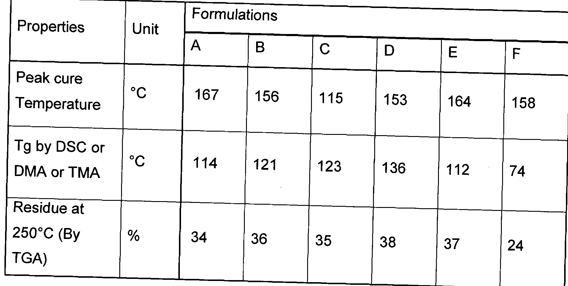
- Table 2 shows basic material properties of the flux residues. Key to performance is controlling these properties. Fraction of residue remaining after reflow is important to cover the solder interconnect which is important to provide additional mechanical strength. Peak residue transition temperature is important to make sure that flux residue remaining on the solder joint is completely transformed into strong solid material capable of adding strength to the solder joint. Glass transition temperature is important to make sure that the materials do not degrade or change properties during high temperature operation or during temperature cycling or thermal shock tests.
Landscapes
- Engineering & Computer Science (AREA)
- Mechanical Engineering (AREA)
- Microelectronics & Electronic Packaging (AREA)
- Manufacturing & Machinery (AREA)
- Computer Hardware Design (AREA)
- Power Engineering (AREA)
- Electric Connection Of Electric Components To Printed Circuits (AREA)
Abstract
Description

Claims
Priority Applications (5)
| Application Number | Priority Date | Filing Date | Title |
|---|---|---|---|
| CN201580032917.2A CN106470794A (en) | 2014-06-19 | 2015-06-19 | Engineering residue solder cream technique |
| KR1020177001772A KR20170035909A (en) | 2014-06-19 | 2015-06-19 | Engineered residue solder paste technology |
| US15/318,829 US20170135227A1 (en) | 2014-06-19 | 2015-06-19 | Engineered Residue Solder Paste Technology |
| JP2016573813A JP2017527102A (en) | 2014-06-19 | 2015-06-19 | Industrial residue solder paste technology |
| EP15733870.8A EP3157704A1 (en) | 2014-06-19 | 2015-06-19 | Engineered residue solder paste technology |
Applications Claiming Priority (2)
| Application Number | Priority Date | Filing Date | Title |
|---|---|---|---|
| IN2984/CHE/2014 | 2014-06-19 | ||
| IN2984CH2014 | 2014-06-19 |
Publications (1)
| Publication Number | Publication Date |
|---|---|
| WO2015193684A1 true WO2015193684A1 (en) | 2015-12-23 |
Family
ID=53502706
Family Applications (1)
| Application Number | Title | Priority Date | Filing Date |
|---|---|---|---|
| PCT/GB2015/051797 WO2015193684A1 (en) | 2014-06-19 | 2015-06-19 | Engineered residue solder paste technology |
Country Status (6)
| Country | Link |
|---|---|
| US (1) | US20170135227A1 (en) |
| EP (1) | EP3157704A1 (en) |
| JP (1) | JP2017527102A (en) |
| KR (1) | KR20170035909A (en) |
| CN (1) | CN106470794A (en) |
| WO (1) | WO2015193684A1 (en) |
Cited By (4)
| Publication number | Priority date | Publication date | Assignee | Title |
|---|---|---|---|---|
| WO2016156853A1 (en) * | 2015-04-01 | 2016-10-06 | Alpha Metals, Inc. | Engineered polymer-based electronic materials |
| CN107442924A (en) * | 2016-05-31 | 2017-12-08 | 松下知识产权经营株式会社 | Solder material |
| KR20180024508A (en) * | 2016-08-30 | 2018-03-08 | 현대자동차주식회사 | Flux compositon comprising carbon component, solder paste comprising the same and method of soldering |
| US20220009042A1 (en) * | 2019-01-24 | 2022-01-13 | Koki Company Limited | Flux and solder paste |
Families Citing this family (5)
| Publication number | Priority date | Publication date | Assignee | Title |
|---|---|---|---|---|
| KR102320111B1 (en) * | 2017-09-01 | 2021-11-01 | 주식회사 엘지화학 | Protective circuit welding member and method for forming welding member |
| CN108941970B (en) * | 2018-08-15 | 2021-03-12 | 句容协鑫集成科技有限公司 | High-precision welding strip for welding junction box and preparation method thereof |
| CN111015021B (en) * | 2019-12-30 | 2021-12-07 | 苏州优诺电子材料科技有限公司 | Low-temperature lead-free soldering paste and preparation method thereof |
| JP2021136448A (en) * | 2020-02-26 | 2021-09-13 | リテルフューズ、インコーポレイテッド | Self-limiting heater |
| KR102375410B1 (en) * | 2020-12-10 | 2022-03-17 | 한국전자기술연구원 | Lead-free solder paste and preparing method thereof |
Citations (6)
| Publication number | Priority date | Publication date | Assignee | Title |
|---|---|---|---|---|
| US3791027A (en) * | 1971-06-30 | 1974-02-12 | Ibm | Soldering method |
| US5167729A (en) * | 1989-08-08 | 1992-12-01 | Nippondenso Co., Ltd. | Soldering flux |
| WO1997007542A1 (en) * | 1995-08-11 | 1997-02-27 | Kirsten Kenneth J | Epoxy resin based solder paste |
| JP2001219294A (en) * | 1999-12-03 | 2001-08-14 | Tdk Corp | Thermosetting flux for soldering and soldering method |
| US6367150B1 (en) * | 1997-09-05 | 2002-04-09 | Northrop Grumman Corporation | Solder flux compatible with flip-chip underfill material |
| EP1914035A1 (en) * | 2005-08-11 | 2008-04-23 | Senju Metal Industry Co., Ltd. | Lead free solder paste and application thereof |
Family Cites Families (11)
| Publication number | Priority date | Publication date | Assignee | Title |
|---|---|---|---|---|
| JP3797990B2 (en) * | 2003-08-08 | 2006-07-19 | 株式会社東芝 | Thermosetting flux and solder paste |
| JP4134976B2 (en) * | 2004-10-26 | 2008-08-20 | 松下電器産業株式会社 | Solder bonding method |
| CN100533701C (en) * | 2005-03-16 | 2009-08-26 | 松下电器产业株式会社 | Method of flip chip mounting using conductive grain |
| JP4677968B2 (en) * | 2006-09-29 | 2011-04-27 | 株式会社村田製作所 | Solder paste and joined parts |
| JP2010074086A (en) * | 2008-09-22 | 2010-04-02 | Panasonic Corp | Cream solder and method of manufacturing mounting structure using the same |
| JP5482605B2 (en) * | 2010-09-27 | 2014-05-07 | パナソニック株式会社 | Electronic component mounting method |
| WO2012043764A1 (en) * | 2010-09-30 | 2012-04-05 | 日立化成工業株式会社 | Adhesive composition, method for manufacturing semiconductor device, and semiconductor device |
| JP5853146B2 (en) * | 2011-08-24 | 2016-02-09 | パナソニックIpマネジメント株式会社 | Thermosetting resin composition and circuit board |
| EP2763515A4 (en) * | 2011-09-30 | 2015-07-15 | Murata Manufacturing Co | Electronic device, joining material, and method for producing electronic device |
| JP2013094781A (en) * | 2011-10-27 | 2013-05-20 | Denso Corp | Solder paste |
| JP2014072308A (en) * | 2012-09-28 | 2014-04-21 | Sanken Electric Co Ltd | Manufacturing method of semiconductor device and semiconductor device |
-
2015
- 2015-06-19 WO PCT/GB2015/051797 patent/WO2015193684A1/en active Application Filing
- 2015-06-19 CN CN201580032917.2A patent/CN106470794A/en active Pending
- 2015-06-19 KR KR1020177001772A patent/KR20170035909A/en not_active Application Discontinuation
- 2015-06-19 JP JP2016573813A patent/JP2017527102A/en active Pending
- 2015-06-19 US US15/318,829 patent/US20170135227A1/en not_active Abandoned
- 2015-06-19 EP EP15733870.8A patent/EP3157704A1/en not_active Withdrawn
Patent Citations (6)
| Publication number | Priority date | Publication date | Assignee | Title |
|---|---|---|---|---|
| US3791027A (en) * | 1971-06-30 | 1974-02-12 | Ibm | Soldering method |
| US5167729A (en) * | 1989-08-08 | 1992-12-01 | Nippondenso Co., Ltd. | Soldering flux |
| WO1997007542A1 (en) * | 1995-08-11 | 1997-02-27 | Kirsten Kenneth J | Epoxy resin based solder paste |
| US6367150B1 (en) * | 1997-09-05 | 2002-04-09 | Northrop Grumman Corporation | Solder flux compatible with flip-chip underfill material |
| JP2001219294A (en) * | 1999-12-03 | 2001-08-14 | Tdk Corp | Thermosetting flux for soldering and soldering method |
| EP1914035A1 (en) * | 2005-08-11 | 2008-04-23 | Senju Metal Industry Co., Ltd. | Lead free solder paste and application thereof |
Cited By (10)
| Publication number | Priority date | Publication date | Assignee | Title |
|---|---|---|---|---|
| WO2016156853A1 (en) * | 2015-04-01 | 2016-10-06 | Alpha Metals, Inc. | Engineered polymer-based electronic materials |
| US20180056455A1 (en) * | 2015-04-01 | 2018-03-01 | Alpha Assembly Solutions Inc. | Engineered Polymer-Based Electronic Materials |
| US10682732B2 (en) * | 2015-04-01 | 2020-06-16 | Alpha Assembly Solutions Inc. | Engineered polymer-based electronic materials |
| CN107442924A (en) * | 2016-05-31 | 2017-12-08 | 松下知识产权经营株式会社 | Solder material |
| KR20180024508A (en) * | 2016-08-30 | 2018-03-08 | 현대자동차주식회사 | Flux compositon comprising carbon component, solder paste comprising the same and method of soldering |
| CN107775209A (en) * | 2016-08-30 | 2018-03-09 | 现代自动车株式会社 | The solder flux composition of carbonaceous component, the soft solder paste and soft soldering method for including it |
| KR101886085B1 (en) * | 2016-08-30 | 2018-08-07 | 현대자동차 주식회사 | Flux compositon comprising carbon component, solder paste comprising the same and method of soldering |
| US10272511B2 (en) | 2016-08-30 | 2019-04-30 | Hyundai Motor Company | Flux composition containing carbon component, solder paste containing the same, and soldering method |
| CN107775209B (en) * | 2016-08-30 | 2020-12-01 | 现代自动车株式会社 | Flux composition containing carbon component, solder paste containing the same, and soldering method |
| US20220009042A1 (en) * | 2019-01-24 | 2022-01-13 | Koki Company Limited | Flux and solder paste |
Also Published As
| Publication number | Publication date |
|---|---|
| EP3157704A1 (en) | 2017-04-26 |
| CN106470794A (en) | 2017-03-01 |
| KR20170035909A (en) | 2017-03-31 |
| JP2017527102A (en) | 2017-09-14 |
| US20170135227A1 (en) | 2017-05-11 |
Similar Documents
| Publication | Publication Date | Title |
|---|---|---|
| US20170135227A1 (en) | Engineered Residue Solder Paste Technology | |
| US9802275B2 (en) | Rosin-free thermosetting flux formulations | |
| US8222751B2 (en) | Electroconductive bonding material and electronic apparatus | |
| JP5204241B2 (en) | Semiconductor mounting structure and manufacturing method thereof | |
| KR100977163B1 (en) | Solder adhesive and the manufacturing method thereof and the electric device comprising thereof | |
| JP6365841B2 (en) | Mounting structure and manufacturing method thereof | |
| JP6310954B2 (en) | Conductive adhesive and method for manufacturing electronic substrate | |
| CA2595518C (en) | Semiconductor device | |
| US11495564B2 (en) | Electronic-part-reinforcing thermosetting resin composition, semiconductor device, and method for fabricating the semiconductor device | |
| JP6313669B2 (en) | Conductive material and connection structure | |
| JP5256681B2 (en) | Semiconductor device, printed wiring board for semiconductor device, and copper-clad laminate | |
| JP2006035259A (en) | Solder paste | |
| Shi et al. | Investigation of various board-level underfills and adhesives for CTBGA bend performance enhancements in lead-free portable electronic products | |
| JP6328996B2 (en) | Conductive paste, connection structure, and manufacturing method of connection structure | |
| JP7277289B2 (en) | Conductive material, connection structure, and method for manufacturing connection structure | |
| KR20220019708A (en) | Conductive material, bonded structure, and manufacturing method of bonded structure | |
| JP2021096904A (en) | Conductive material, connection structure and method for producing connection structure | |
| Ghaffarian | BOK─ Underfill Optimization for FPGA Package/Assembly | |
| TWI627226B (en) | Dual-side reinforcement flux for encapsulation | |
| US7926696B2 (en) | Composition | |
| JP7284699B2 (en) | Conductive material, connection structure, and method for manufacturing connection structure | |
| JP7316109B2 (en) | Conductive material, connection structure, and method for manufacturing connection structure | |
| KR20170118783A (en) | Electrical connection tape | |
| JP5211624B2 (en) | Manufacturing method of semiconductor device and manufacturing method of printed wiring board for semiconductor device | |
| JP2018177987A (en) | Conductive material |
Legal Events
| Date | Code | Title | Description |
|---|---|---|---|
| 121 | Ep: the epo has been informed by wipo that ep was designated in this application |
Ref document number: 15733870 Country of ref document: EP Kind code of ref document: A1 |
|
| WWE | Wipo information: entry into national phase |
Ref document number: 15318829 Country of ref document: US |
|
| ENP | Entry into the national phase |
Ref document number: 2016573813 Country of ref document: JP Kind code of ref document: A |
|
| NENP | Non-entry into the national phase |
Ref country code: DE |
|
| REEP | Request for entry into the european phase |
Ref document number: 2015733870 Country of ref document: EP |
|
| WWE | Wipo information: entry into national phase |
Ref document number: 2015733870 Country of ref document: EP |
|
| ENP | Entry into the national phase |
Ref document number: 20177001772 Country of ref document: KR Kind code of ref document: A |