WO2013132875A1 - Data reception circuit, electronic apparatus, and method of receiving data - Google Patents
Data reception circuit, electronic apparatus, and method of receiving data Download PDFInfo
- Publication number
- WO2013132875A1 WO2013132875A1 PCT/JP2013/001542 JP2013001542W WO2013132875A1 WO 2013132875 A1 WO2013132875 A1 WO 2013132875A1 JP 2013001542 W JP2013001542 W JP 2013001542W WO 2013132875 A1 WO2013132875 A1 WO 2013132875A1
- Authority
- WO
- WIPO (PCT)
- Prior art keywords
- data
- delay
- circuit
- capture
- timing
- Prior art date
Links
Images


Classifications
-
- H—ELECTRICITY
- H04—ELECTRIC COMMUNICATION TECHNIQUE
- H04L—TRANSMISSION OF DIGITAL INFORMATION, e.g. TELEGRAPHIC COMMUNICATION
- H04L7/00—Arrangements for synchronising receiver with transmitter
- H04L7/0054—Detection of the synchronisation error by features other than the received signal transition
- H04L7/0066—Detection of the synchronisation error by features other than the received signal transition detection of error based on transmission code rule
-
- H—ELECTRICITY
- H04—ELECTRIC COMMUNICATION TECHNIQUE
- H04L—TRANSMISSION OF DIGITAL INFORMATION, e.g. TELEGRAPHIC COMMUNICATION
- H04L25/00—Baseband systems
- H04L25/38—Synchronous or start-stop systems, e.g. for Baudot code
- H04L25/40—Transmitting circuits; Receiving circuits
- H04L25/49—Transmitting circuits; Receiving circuits using code conversion at the transmitter; using predistortion; using insertion of idle bits for obtaining a desired frequency spectrum; using three or more amplitude levels ; Baseband coding techniques specific to data transmission systems
- H04L25/4902—Pulse width modulation; Pulse position modulation
Landscapes
- Engineering & Computer Science (AREA)
- Computer Networks & Wireless Communication (AREA)
- Signal Processing (AREA)
- Physics & Mathematics (AREA)
- Spectroscopy & Molecular Physics (AREA)
- Dc Digital Transmission (AREA)
Abstract
Provided are a data reception circuit, an electronic apparatus, and a method of receiving data which achieve accommodation of multiple bits in pulse width modulation without providing a PLL circuit. This data reception circuit (100) which receives data modulated by pulse width modulation having two or more types of step sizes includes a delay circuit (110) which delays data, a reading timing generation circuit (130) which sequentially delays output of the delay circuit (110) and which generates a plurality of reading timings having two or more types of step sizes, a data reading circuit (140) which reads predetermined data at a plurality of reading timings which have been generated by the reading timing generation circuit (130), and a pulse width detection circuit (150) which detects received data on the basis of the read data which have been read at each read-timing at the data reading circuit (140).
Description
本発明は、データ受信回路、電子機器、及びデータ受信方法等に関する。
The present invention relates to a data receiving circuit, an electronic device, a data receiving method, and the like.
近年、液晶パネルや有機EL(Electro-Luminescence)パネル等の表示パネルの画面サイズの大型化、高解像度化、3D化等に伴い、表示パネルを駆動する表示ドライバーに供給する表示データの転送周波数が飛躍的に増大している。そのため、表示データが転送されるバス幅を広げたり、表示データのデータ転送周波数をより一層高くしたりすることで対応する必要がある。
In recent years, with the increase in screen size, resolution, 3D, etc. of display panels such as liquid crystal panels and organic EL (Electro-Luminescence) panels, the transfer frequency of display data supplied to the display driver that drives the display panel It has increased dramatically. Therefore, it is necessary to cope with the problem by widening the bus width to which display data is transferred, or by further increasing the data transfer frequency of display data.
ところが、表示データが転送されるバスをCMOS(Complementary Metal Oxide Semiconductor)により構成されるバッファーで駆動する場合、バス幅を広げると、EMI(Electro Magnetic Interface)ノイズや電源の揺れが大きくなるという問題がある。そこで、LVDS(Low Voltage Differential Signaling)や、Mini-LVDS等の差動インターフェイス技術を用いて表示データを転送することが行われることが多い。
However, when a bus to which display data is transferred is driven by a buffer composed of CMOS (Complementary Metal Oxide Semiconductor), if the bus width is widened, EMI (Electro Magnetic Interface) noise and power fluctuation will increase. is there. Therefore, display data is often transferred using a differential interface technology such as LVDS (Low Voltage Differential Signaling) or Mini-LVDS.
しかしながら、このLVDSやMini-LVDS等の差動インターフェイス技術を用いても、より一層周波数を高める必要があり、現在要求されている周波数においてもクロックの差動信号とデータの差動信号とで波形のずれが生じるという問題が発生しつつある。このため、最近では、クロック及びデータを差動信号に埋め込んだSerDesやこれを改良した種々のインターフェイス技術を用いて、表示データの転送が行われる場合がある。
However, even if this differential interface technology such as LVDS or Mini-LVDS is used, it is necessary to further increase the frequency, and the waveform of the clock differential signal and the data differential signal is also used at the currently required frequency. There is a problem that a shift occurs. For this reason, recently, display data may be transferred using SerDes in which a clock and data are embedded in a differential signal and various interface technologies improved therefrom.
一方、クロック及び表示データ等をパルス幅変調により変調したデータを、伝送ラインを介して送信することも行われている。クロック及びデータをパルス幅変調により変調したデータを、伝送ラインを介して送信する技術については、例えば特許文献1及び特許文献2に開示されている。
On the other hand, data obtained by modulating a clock and display data by pulse width modulation is also transmitted through a transmission line. For example, Patent Literature 1 and Patent Literature 2 disclose a technique for transmitting data obtained by modulating a clock and data by pulse width modulation via a transmission line.
しかしながら、上記のSerDes(Serializer/Deserializer)やこれを改良したインターフェイス技術では、データの転送周波数が、測定機器の限界に達しており、測定機器の実測により性能を補償することが困難な状況になっている。また、これらのインターフェイス技術では、差動信号線の各々について、送信側のみならず受信側にもPLL(Phased-Locked Loop)回路が必要になるという問題がある。更に、データからクロックを復元する等の論理回路の規模が大きくなり、例えば細長いチップ形状で多出力が求められる表示ドライバーにおいては、短辺方向に大きくなり、コスト高や実装上の問題等が生じる。
However, with the above-mentioned SerDes (Serializer / Deserializer) and the improved interface technology, the data transfer frequency has reached the limit of the measuring device, and it becomes difficult to compensate the performance by actual measurement of the measuring device. ing. In addition, these interface technologies have a problem that, for each differential signal line, a PLL (Phased-Locked 必要 Loop) circuit is required not only on the transmission side but also on the reception side. Further, the scale of the logic circuit such as restoring the clock from the data becomes large. For example, in a display driver that requires a long chip shape and multiple outputs, the display driver becomes large in the short side direction, resulting in high costs and mounting problems. .
また、特許文献1及び特許文献2に開示されているように、単純に、パルス幅変調によりデータを送信する場合でも、送信側のみならず受信側にもPLL回路がなければ、高い周波数で多ビット化に対応することが難しいという問題がある。
Further, as disclosed in Patent Document 1 and Patent Document 2, even when data is simply transmitted by pulse width modulation, if there is no PLL circuit on the receiving side as well as on the transmitting side, there are many high frequencies. There is a problem that it is difficult to cope with bit conversion.
本発明は、上記の課題の少なくとも一部を解決するためになされたものであり、以下の形態又は態様として実現することが可能である。
The present invention has been made to solve at least a part of the above problems, and can be realized as the following forms or modes.
(1)本発明の第1の態様は、2種類以上の刻み幅を有するパルス幅変調により変調されたデータを受信するデータ受信回路が、前記データを遅延させるデータ遅延部と、前記データ遅延部の出力を順次遅延させて2種類以上の刻み幅を有する複数の取込タイミングを生成する取込タイミング生成部と、前記取込タイミング生成部によって生成された前記複数の取込タイミングで、所定のデータを取り込むデータ取込部と、前記データ取込部において各取込タイミングで取り込まれた取込データに基づいて受信データを検出する受信データ検出部とを含む。
(1) According to a first aspect of the present invention, a data receiving circuit that receives data modulated by pulse width modulation having two or more types of step widths, a data delay unit that delays the data, and the data delay unit A capture timing generation unit that sequentially delays the output of the plurality of capture timings to generate a plurality of capture timings having two or more step sizes, and a plurality of capture timings generated by the capture timing generation unit, A data capture unit that captures data; and a reception data detection unit that detects reception data based on captured data captured at each capture timing in the data capture unit.
本態様においては、2種類以上の刻み幅を有するパルス幅変調により変調させたデータを遅延するデータ遅延部の出力を順次遅延させて、刻み幅に対応した取込タイミングを生成する。これにより、受信側では、PLL回路を設けることなく、多ビットのパルス幅変調されたデータを受信することができるので、パルス幅変調の多ビット化を実現することができる。これにより、本態様におけるデータ受信回路を備える集積回路の小型化に寄与することができる。
In this aspect, the output of the data delay unit that delays the data modulated by pulse width modulation having two or more types of step widths is sequentially delayed to generate the capture timing corresponding to the step size. As a result, multi-bit pulse width modulated data can be received on the receiving side without providing a PLL circuit, so that multi-bit pulse width modulation can be realized. Thereby, it can contribute to size reduction of an integrated circuit provided with the data receiving circuit in this mode.
(2)本発明の第2の態様に係るデータ受信回路では、第1の態様において、前記複数の取込タイミングは、基準タイミングに近い取込タイミングほど刻み幅が小さくなる。
(2) In the data receiving circuit according to the second aspect of the present invention, in the first aspect, the plurality of capture timings have smaller increments as the capture timing is closer to the reference timing.
本態様においては、基準タイミングに近い取込タイミングほど刻み幅が小さくなるように複数の取込タイミングを生成するようにした。例えば、基準タイミングは、データの変化タイミング(具体的には、立ち上がりエッジ)とすることができる。これにより、例えば基準タイミングを遅延させて複数の取込タイミングを生成する場合に、基準タイミングからの遅延精度によって刻み幅を規定することができる。従って、基準タイミングと各取込タイミングとのタイミング差にかかわらず精度良く規定された各取込タイミングにおいてデータを取り込むことができる。その結果、例えばデータの立ち上がりエッジを基準にパルス幅変調されたデータのHレベルの幅を検出する場合に、限られた期間内により多くの複数の取込タイミングを簡素の遅延回路によって生成することができ、パルス幅変調の多ビット化が可能になる。
In this aspect, a plurality of capture timings are generated so that the step size becomes smaller as the capture timing is closer to the reference timing. For example, the reference timing can be a data change timing (specifically, a rising edge). Thereby, for example, when the plurality of capture timings are generated by delaying the reference timing, the step size can be defined by the delay accuracy from the reference timing. Therefore, data can be captured at each capture timing defined with high precision regardless of the timing difference between the reference timing and each capture timing. As a result, for example, when detecting the H level width of the pulse width modulated data with reference to the rising edge of the data, a plurality of capture timings are generated by a simple delay circuit within a limited period. This makes it possible to increase the number of bits of pulse width modulation.
(3)本発明の第3の態様に係るデータ受信回路では、第1の態様において、前記複数の取込タイミングは、基準タイミングに近い取込タイミングほど刻み幅が大きくなる。
(3) In the data receiving circuit according to the third aspect of the present invention, in the first aspect, the plurality of capture timings have larger increments as the capture timing is closer to the reference timing.
本態様においては、基準タイミングに近い取込タイミングほど刻み幅が大きくなるように複数の取込タイミングを生成するようにした。例えば、基準タイミングは、データの変化タイミング(具体的には、立ち上がりエッジ)とすることができる。これにより、例えば基準タイミングを遅延させて複数の取込タイミングを生成する場合に、基準タイミングからの遅延精度によって刻み幅を規定することができる。従って、基準タイミングと各取込タイミングとのタイミング差にかかわらず精度良く規定された各取込タイミングにおいてデータを取り込むことができる。その結果、パルス幅変調されたデータのLレベル固定期間の終了タイミングである立ち上がりエッジを基準にパルス幅変調されたデータのLレベルの幅を検出する場合に、限られた期間内により多くの複数の取込タイミングを簡素の遅延回路によって生成することができ、パルス幅変調の多ビット化が可能になる。
In this aspect, a plurality of capture timings are generated so that the step size becomes larger as the capture timing is closer to the reference timing. For example, the reference timing can be a data change timing (specifically, a rising edge). Thereby, for example, when the plurality of capture timings are generated by delaying the reference timing, the step size can be defined by the delay accuracy from the reference timing. Therefore, data can be captured at each capture timing defined with high precision regardless of the timing difference between the reference timing and each capture timing. As a result, when the width of the L level of the pulse width modulated data is detected with reference to the rising edge that is the end timing of the L level fixed period of the pulse width modulated data, a larger number of data are detected within the limited period. Can be generated by a simple delay circuit, and the number of bits of pulse width modulation can be increased.
(4)本発明の第4の態様に係るデータ受信回路では、第1の態様乃至第3の態様のいずれかにおいて、前記データ取込部は、前記複数の取込タイミングの各々に対応して設けられ前記データの受信に先立って初期化される複数のフリップフロップを含み、前記複数のフリップフロップの各々は、対応する取込タイミングで変化する取込クロックに基づいて、前記所定のデータを取り込む。
(4) In the data reception circuit according to the fourth aspect of the present invention, in any one of the first aspect to the third aspect, the data capture unit corresponds to each of the plurality of capture timings. A plurality of flip-flops that are provided and initialized prior to the reception of the data, and each of the plurality of flip-flops captures the predetermined data based on a capture clock that changes at a corresponding capture timing .
本態様によれば、複数のフリップフロップのうち、保持するデータが所定のデータであるフリップフロップと、保持するデータが初期値であるフリップフロップとによって、データのパルス幅を検出することができるようになる。
According to this aspect, the pulse width of the data can be detected by the flip-flop in which the retained data is predetermined data and the flip-flop in which the retained data is the initial value among the plurality of flip-flops. become.
(5)本発明の第5の態様に係るデータ受信回路は、第1の態様乃至第4の態様のいずれかにおいて、前記データ遅延部の電源電圧に対応した制御値が設定される第1の遅延設定レジスターを含み、前記データ遅延部の電源電圧を、前記第1の遅延設定レジスターに設定された前記制御値に対応した電圧に設定する。
(5) In the data reception circuit according to the fifth aspect of the present invention, in any one of the first to fourth aspects, a control value corresponding to a power supply voltage of the data delay unit is set. Including a delay setting register, and sets the power supply voltage of the data delay unit to a voltage corresponding to the control value set in the first delay setting register.
本態様によれば、データ遅延部の電源電圧を変更することによって、データの遅延値を調整するようにしたので、非常に簡素な構成及び制御により、取込タイミングを調整することができる。
According to this aspect, since the data delay value is adjusted by changing the power supply voltage of the data delay unit, the capture timing can be adjusted with a very simple configuration and control.
(6)本発明の第6の態様に係るデータ受信回路は、第1の態様乃至第5の態様のいずれかにおいて、前記データ遅延部と前記取込タイミング生成部との間に設けられ、前記データ遅延部の出力をバッファリングしてから前記取込タイミング生成部に出力する出力バッファーと、前記出力バッファーの電源電圧に対応した制御値が設定される第2の遅延設定レジスターとを含み、前記出力バッファーの電源電圧を、前記第2の遅延設定レジスターに設定された前記制御値に対応した電圧に設定する。
(6) A data reception circuit according to a sixth aspect of the present invention is provided between the data delay unit and the capture timing generation unit in any one of the first to fifth aspects, An output buffer for buffering the output of the data delay unit and then outputting to the capture timing generation unit; and a second delay setting register for setting a control value corresponding to the power supply voltage of the output buffer, The power supply voltage of the output buffer is set to a voltage corresponding to the control value set in the second delay setting register.
本態様によれば、データ遅延部の出力に接続される出力バッファーの電源電圧を変更することによって、データの遅延値を調整するようにしたので、非常に簡素な構成及び制御により、取込タイミングを調整することができる。
According to this aspect, since the data delay value is adjusted by changing the power supply voltage of the output buffer connected to the output of the data delay unit, the capture timing can be adjusted with a very simple configuration and control. Can be adjusted.
(7)本発明の第7の態様に係るデータ受信回路では、第1の態様乃至第6の態様のいずれかにおいて、前記取込タイミング生成部は、各々が抵抗素子及び容量素子により構成された複数の遅延回路の各々が縦続に接続される構成を有し、各遅延回路の出力を各取込タイミングとして出力する。
(7) In the data reception circuit according to the seventh aspect of the present invention, in any one of the first aspect to the sixth aspect, each of the capture timing generation units is configured by a resistance element and a capacitance element. Each of the plurality of delay circuits is connected in cascade, and the output of each delay circuit is output as each capture timing.
本態様によれば、複数の遅延回路の各々を縦続に接続し、各遅延回路の出力を取込タイミングとして出力するようにしたので、簡素な構成の遅延回路により、パルス幅変調の多ビット化に対応できるデータ受信回路を提供することができる。
According to this aspect, since each of the plurality of delay circuits is connected in cascade and the output of each delay circuit is output as the capture timing, the multi-bit pulse width modulation can be achieved with the delay circuit having a simple configuration. Can be provided.
(8)本発明の第8の態様に係るデータ受信回路は、第7の態様において、各々が対応する遅延回路の出力に接続された複数のクロックバッファーと、前記複数のクロックバッファーの電源電圧に対応した制御値が設定される第3の遅延設定レジスターとを含み、前記複数のクロックバッファーの電源電圧を、前記第3の遅延設定レジスターに設定された前記制御値に対応した電圧に設定する。
(8) According to an eighth aspect of the present invention, there is provided a data receiving circuit according to the seventh aspect, wherein a plurality of clock buffers each connected to an output of a corresponding delay circuit and a power supply voltage of the plurality of clock buffers are used. And a third delay setting register in which a corresponding control value is set, and the power supply voltages of the plurality of clock buffers are set to voltages corresponding to the control value set in the third delay setting register.
本態様によれば、各取込タイミングに対応した取込クロックを出力するクロックバッファーの電源電圧を変更するようにしたので、非常に簡素な構成及び制御により、取込タイミングを調整することができる。
According to this aspect, since the power supply voltage of the clock buffer that outputs the capture clock corresponding to each capture timing is changed, the capture timing can be adjusted with a very simple configuration and control. .
(9)本発明の第9の態様に係るデータ受信回路は、第7の態様又は第8の態様において、前記複数の遅延回路の終端部に接続される終端回路と、前記終端回路の容量値に対応した制御値が設定される第4の遅延設定レジスターとを含み、前記終端回路の容量値を、前記第4の遅延設定レジスターに設定された前記制御値に対応した容量値に設定する。
(9) In the data reception circuit according to the ninth aspect of the present invention, in the seventh aspect or the eighth aspect, a termination circuit connected to termination units of the plurality of delay circuits, and a capacitance value of the termination circuit And a fourth delay setting register in which a control value corresponding to is set, and the capacitance value of the termination circuit is set to a capacitance value corresponding to the control value set in the fourth delay setting register.
本態様によれば、複数の遅延回路の終端部に接続される終端回路の容量値を変更することによって、データの遅延値を調整するようにしたので、非常に簡素な構成及び制御により、取込タイミングを調整することができる。
According to this aspect, since the delay value of the data is adjusted by changing the capacitance value of the termination circuit connected to the termination units of the plurality of delay circuits, the data can be obtained with a very simple configuration and control. Can be adjusted.
(10)本発明の第10の態様に係るデータ受信回路は、第7の態様乃至第9の態様のいずれかにおいて、前記遅延回路を構成する容量素子の容量値に対応した制御値が設定される第5の遅延設定レジスターを含み、前記容量素子の容量値を、前記第5の遅延設定レジスターに設定された前記制御値に対応した容量値に設定する。
(10) In the data receiving circuit according to the tenth aspect of the present invention, in any of the seventh aspect to the ninth aspect, a control value corresponding to the capacitance value of the capacitive element constituting the delay circuit is set. And a capacitance value of the capacitive element is set to a capacitance value corresponding to the control value set in the fifth delay setting register.
本態様によれば、複数の遅延回路の各々を構成する容量素子の容量値を変更することによって、データの遅延値を調整するようにしたので、非常に簡素な構成及び制御により、取込タイミングを調整することができる。
According to this aspect, since the delay value of the data is adjusted by changing the capacitance value of the capacitive element that constitutes each of the plurality of delay circuits, the capture timing can be adjusted with a very simple configuration and control. Can be adjusted.
(11)本発明の第11の態様に係るデータ受信回路は、第7の態様乃至第10の態様のいずれかにおいて、対応する取込タイミングの出力に先立って、前記複数の遅延回路の各々を構成する容量素子に充電された電荷を初期化する容量初期化回路を含む。
(11) A data receiving circuit according to an eleventh aspect of the present invention is the data receiving circuit according to any one of the seventh aspect to the tenth aspect, wherein each of the plurality of delay circuits is set prior to output of the corresponding capture timing. A capacitor initialization circuit is included that initializes the electric charge charged in the capacitor element.
本態様によれば、データが繰り返し受信される場合でも、複数の遅延回路は、取込タイミングを精度良く遅延させることができる。
According to this aspect, even when data is repeatedly received, the plurality of delay circuits can delay the capture timing with high accuracy.
(12)本発明の第12の態様は、電子機器が、第1の態様乃至第11の態様のいずれか記載のデータ受信回路を含む。
(12) In a twelfth aspect of the present invention, the electronic device includes the data receiving circuit according to any one of the first to eleventh aspects.
本態様によれば、受信側でPLL回路を設けることなく、測定機器の測定限界を超えた周波数であっても、低コストで、大容量のデータを高速に送受信することができる電子機器の提供に寄与することができる。
According to this aspect, it is possible to provide an electronic device capable of transmitting and receiving a large amount of data at high speed at a low cost even when the frequency exceeds the measurement limit of the measuring device without providing a PLL circuit on the receiving side. Can contribute.
(13)本発明の第13の態様は、2種類以上の刻み幅を有するパルス幅変調により変調されたデータを受信するデータ受信方法が、前記データの変化タイミングに対応した基準タイミングに基づいて決められる2種類以上の刻み幅を有する複数の取込タイミングで、前記データを取り込むデータ取込ステップと、前記データ取込ステップにおいて前記複数の取込タイミングで取り込まれた取込データに基づいて受信データを検出する受信データ検出ステップとを含む。
(13) In a thirteenth aspect of the present invention, a data reception method for receiving data modulated by pulse width modulation having two or more types of step widths is determined based on a reference timing corresponding to the data change timing. A data capture step for capturing the data at a plurality of capture timings having two or more step sizes, and received data based on the capture data captured at the plurality of capture timings in the data capture step And a received data detecting step for detecting.
本態様においては、2種類以上の刻み幅を有するパルス幅変調により変調させたデータの変化タイミングに対応した基準タイミングに基づいて、取込タイミングを生成する。これにより、受信側では、PLL回路を設けることなく、多ビットのパルス幅変調されたデータを受信することができるので、パルス幅変調の多ビット化を実現することができる。
In this embodiment, the capture timing is generated based on the reference timing corresponding to the change timing of the data modulated by the pulse width modulation having two or more kinds of step widths. As a result, multi-bit pulse width modulated data can be received on the receiving side without providing a PLL circuit, so that multi-bit pulse width modulation can be realized.
(14)本発明の第14の態様に係るデータ受信方法は、第13の態様において、前記基準タイミングを順次遅延させることにより前記複数の取込タイミングを生成する取込タイミング生成ステップを含み、前記複数の取込タイミングは、前記基準タイミングに近い取込タイミングほど刻み幅が小さくなる。
(14) A data reception method according to a fourteenth aspect of the present invention includes, in the thirteenth aspect, a capture timing generation step of generating the plurality of capture timings by sequentially delaying the reference timing, The plurality of capture timings have smaller increments as the capture timing is closer to the reference timing.
本態様においては、基準タイミングに近い取込タイミングほど刻み幅が小さくなるように複数の取込タイミングを生成するようにした。例えば、基準タイミングは、データの変化タイミング(具体的には、立ち上がりエッジ)とすることができる。これにより、基準タイミングからの遅延精度によって刻み幅を規定することができ、基準タイミングと各取込タイミングとのタイミング差にかかわらず精度良く規定された各取込タイミングにおいてデータを取り込むことができる。その結果、限られた期間内により多くの複数の取込タイミングを簡素の遅延手段によって生成することができ、パルス幅変調の多ビット化が可能になる。
In this aspect, a plurality of capture timings are generated so that the step size becomes smaller as the capture timing is closer to the reference timing. For example, the reference timing can be a data change timing (specifically, a rising edge). Thereby, the step size can be defined by the delay accuracy from the reference timing, and data can be captured at each capture timing that is defined accurately regardless of the timing difference between the reference timing and each capture timing. As a result, a plurality of capture timings can be generated by simple delay means within a limited period, and multi-bit pulse width modulation can be achieved.
(15)本発明の第15の態様に係るデータ受信方法は、第14の態様において、前記基準タイミングを遅延させる遅延手段の電源電圧、及び該遅延手段を構成する容量素子の容量値の少なくとも一方を調整する遅延調整ステップを含み、前記取込タイミング生成ステップは、前記遅延調整ステップにおいて調整された前記遅延手段により前記基準タイミングを順次遅延させて、前記複数の取込タイミングを生成する。
(15) The data receiving method according to a fifteenth aspect of the present invention is the data receiving method according to the fourteenth aspect, wherein at least one of the power supply voltage of the delay means for delaying the reference timing and the capacitance value of the capacitive element constituting the delay means The capture timing generation step generates the plurality of capture timings by sequentially delaying the reference timing by the delay means adjusted in the delay adjustment step.
本態様によれば、簡素な構成及び制御により、複数の取込タイミングを生成することができるようになる。
According to this aspect, a plurality of capture timings can be generated with a simple configuration and control.
(16)本発明の第16の態様に係るデータ受信方法では、第15の態様において、前記遅延調整ステップは、前記データのパルス幅が最短となる第1のデータと、前記データのパルス幅が最長となる第2のデータとを用いて、前記遅延手段の遅延値を調整する。
(16) In the data reception method according to the sixteenth aspect of the present invention, in the fifteenth aspect, the delay adjustment step includes: the first data having the shortest pulse width of the data; and the pulse width of the data The delay value of the delay means is adjusted using the longest second data.
本態様によれば、パルス幅が最短となる第1のデータとパルス幅が最長となる第2のデータとを用いて遅延手段の遅延値を調整するようにしたので、非常に少ないステップで、複数の刻み幅に対応した取込タイミングを調整することができるようになる。
According to this aspect, since the delay value of the delay means is adjusted using the first data having the shortest pulse width and the second data having the longest pulse width, the number of steps is very small. The capture timing corresponding to a plurality of step sizes can be adjusted.
以下、本発明の実施の形態について図面を用いて詳細に説明する。なお、以下に説明する実施の形態は、特許請求の範囲に記載された本発明の内容を不当に限定するものではない。また以下で説明される構成のすべてが本発明の課題を解決するために必須の構成要件であるとは限らない。
Hereinafter, embodiments of the present invention will be described in detail with reference to the drawings. The embodiments described below do not unduly limit the contents of the present invention described in the claims. In addition, all of the configurations described below are not necessarily indispensable configuration requirements for solving the problems of the present invention.
〔第1の実施形態〕
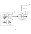
図1に、本発明の第1の実施形態に係るデータ受信回路が適用された電子機器の構成例のブロック図を示す。 [First Embodiment]
FIG. 1 shows a block diagram of a configuration example of an electronic device to which a data receiving circuit according to the first embodiment of the present invention is applied.
図1に、本発明の第1の実施形態に係るデータ受信回路が適用された電子機器の構成例のブロック図を示す。 [First Embodiment]
FIG. 1 shows a block diagram of a configuration example of an electronic device to which a data receiving circuit according to the first embodiment of the present invention is applied.
電子機器10は、表示データ供給装置20と、表示ドライバー30と、表示パネル40とを備えている。表示データ供給装置20は、表示データ生成回路22と、データ送信回路24と、PLL回路26と、送信制御部28とを備えている。表示ドライバー30は、データ受信回路100と、駆動回路32とを備えている。表示データ供給装置20の機能は、例えば、いわゆる表示コントローラーや中央演算処理装置(Central Processing Unit)等によって実現される。表示パネル40は、複数の画素がマトリックス状に配列される液晶パネルや有機ELパネル等である。表示ドライバー30は、表示データ供給装置20から供給される表示データに基づいて表示パネル40を構成する画素を駆動し、表示データに対応した画像を表示させる。
The electronic device 10 includes a display data supply device 20, a display driver 30, and a display panel 40. The display data supply device 20 includes a display data generation circuit 22, a data transmission circuit 24, a PLL circuit 26, and a transmission control unit 28. The display driver 30 includes a data receiving circuit 100 and a driving circuit 32. The function of the display data supply device 20 is realized by, for example, a so-called display controller, a central processing unit (Central Processing Unit), or the like. The display panel 40 is a liquid crystal panel or an organic EL panel in which a plurality of pixels are arranged in a matrix. The display driver 30 drives the pixels constituting the display panel 40 based on the display data supplied from the display data supply device 20, and displays an image corresponding to the display data.
表示データ供給装置20において、表示データ生成回路22は、表示パネル40に表示される画像に対応した表示データを生成する。PLL回路26は、第1の実施形態におけるパルス幅変調の刻み幅に対応したクロックを生成し、データ送信回路24に出力する。データ送信回路24は、表示データ生成回路22によって生成された表示データを、PLL回路26からのクロックを用いてパルス幅変調し、パルス幅変調後のデータを表示ドライバー30に対して送信する処理を行う。具体的には、データ送信回路24は、送信データの変化タイミングを表示データにより変調することで、パルス幅変調を行う。送信制御部28は、表示データ生成回路22、データ送信回路24、及びPLL回路26の制御を司る。
In the display data supply device 20, the display data generation circuit 22 generates display data corresponding to the image displayed on the display panel 40. The PLL circuit 26 generates a clock corresponding to the step width of the pulse width modulation in the first embodiment and outputs it to the data transmission circuit 24. The data transmission circuit 24 performs a process of performing pulse width modulation on the display data generated by the display data generation circuit 22 using the clock from the PLL circuit 26 and transmitting the data after the pulse width modulation to the display driver 30. Do. Specifically, the data transmission circuit 24 performs pulse width modulation by modulating the change timing of transmission data with display data. The transmission control unit 28 controls the display data generation circuit 22, the data transmission circuit 24, and the PLL circuit 26.
表示ドライバー30において、データ受信回路100は、表示データ供給装置20によって送信されたデータを受信する処理を行う。データ受信回路100は、第1の実施形態におけるパルス幅変調の刻み幅に基づいて、受信データの変化タイミングに対応した受信データを検出し、検出した受信データを受信した表示データとして駆動回路32に出力する。駆動回路32は、データ受信回路100によって受信されたデータに基づいて、表示パネル40を駆動する。
In the display driver 30, the data receiving circuit 100 performs a process of receiving data transmitted by the display data supply device 20. The data receiving circuit 100 detects the received data corresponding to the change timing of the received data based on the step width of the pulse width modulation in the first embodiment, and the detected received data is sent to the drive circuit 32 as the received display data. Output. The drive circuit 32 drives the display panel 40 based on the data received by the data receiving circuit 100.
図2に、第1の実施形態におけるパルス幅変調の説明図を示す。図2は、1サイクル期間において4ビットの表示データに対してパルス幅変調を行った例を表す。
FIG. 2 is an explanatory diagram of pulse width modulation in the first embodiment. FIG. 2 shows an example in which pulse width modulation is performed on 4-bit display data in one cycle period.
第1の実施形態におけるパルス幅変調が行われた受信データでは、データの立ち上がりエッジが基準タイミングとして抽出され、1サイクル期間が規定される。1サイクル期間の先頭には、必ずHレベルに固定される所定のHレベル固定期間t0が設けられ、1サイクル期間の終了には、必ずLレベルに固定される所定のLレベル固定期間t1が設けられる。受信データにおいては、1サイクル期間内でHレベル固定期間t0及びLレベル固定期間t1を除いた期間内に、2種類以上の刻み幅で、15カ所の立ち下がりエッジの位置が規定される。Hレベル固定期間t0が終了する立ち下がりエッジの位置を含めると、1サイクル期間内に16カ所の立ち下がりエッジの位置が規定される。
In the received data subjected to pulse width modulation in the first embodiment, the rising edge of the data is extracted as the reference timing, and one cycle period is defined. A predetermined H level fixing period t0 that is always fixed to the H level is provided at the beginning of one cycle period, and a predetermined L level fixing period t1 that is always fixed to the L level is provided at the end of one cycle period. It is done. In the received data, 15 falling edge positions are defined in two or more step sizes within a period excluding the H level fixed period t0 and the L level fixed period t1 within one cycle period. Including the positions of the falling edges where the H level fixed period t0 ends, the positions of 16 falling edges are defined within one cycle period.
各立ち下がりエッジの位置は、4ビットの表示データの各々に対応する。例えば、基準タイミングを基準としてt0期間後の立ち下がりエッジの位置は、表示データ「(0)16」(=(0000)2)に対応する。また、t0期間後に更に刻み幅tw0が経過した「t0+tw0」期間後の立ち下がりエッジの位置は、表示データ「(1)16」(=(0001)2)に対応する。同様に、基準タイミングを基準として「t0+tw0+tw1」期間後の立ち下がりエッジの位置は、表示データ「(2)16」(=(0010)2)に対応する。そして、基準タイミングを基準として「t0+tw0+tw1+・・・+tw15」期間後の立ち下がりエッジの位置は、表示データ「(F)16」(=(1111)2)に対応する。
The position of each falling edge corresponds to each of 4-bit display data. For example, the position of the falling edge after the period t0 with respect to the reference timing corresponds to the display data “(0) 16 ” (= (0000) 2 ). Further, the position of the falling edge after the “t0 + tw 0 ” period in which the step width tw 0 has elapsed after the t0 period corresponds to the display data “(1) 16 ” (= (0001) 2 ). Similarly, the position of the falling edge after the “t0 + tw 0 + tw 1 ” period with reference to the reference timing corresponds to the display data “(2) 16 ” (= (0010) 2 ). Then, the position of the falling edge after the “t0 + tw 0 + tw 1 +... + Tw 15 ” period with reference to the reference timing corresponds to the display data “(F) 16 ” (= (1111) 2 ).
第1の実施形態では、基準タイミングから遠いほど刻み幅が粗くなるように、各立ち下がりエッジの位置が規定される。即ち、0<tw1<tw2<tw3<・・・<tw14<tw15である。具体的には、第1の実施形態では基準タイミングを遅延させて各刻み幅を規定し、kを1以上の実数とすると、以下の式が成立する。kは、直前の立ち下がりエッジのタイミングを遅延させて各立ち下がりエッジの位置を規定するときの遅延精度に応じて決められる。

In the first embodiment, the position of each falling edge is defined so that the step size becomes coarser as the distance from the reference timing increases. That is, 0 <tw 1 <tw 2 <tw 3 <... <Tw 14 <tw 15 . Specifically, in the first embodiment, when the reference timing is delayed to define each step size and k is a real number of 1 or more, the following equation is established. k is determined according to the delay accuracy when the timing of each falling edge is defined by delaying the timing of the immediately preceding falling edge.
ここで、PLL回路のような複雑な回路を用いることなく、基準タイミングを順次遅延させて、受信データの立ち下がりエッジの位置を規定することを考える。このとき、1サイクル期間のHレベル固定期間t0及びLレベル固定期間t1を除いた期間内に、均等の刻み幅で16カ所の立ち下がりエッジの位置を規定すると、基準タイミングから遠いほど立ち下がりエッジの揺らぎが大きくなる。即ち、基準タイミングから近い立ち下がりエッジの位置については正確に規定することができる一方、基準タイミングから遠い立ち下がりエッジの位置については、素子ばらつき等に起因して正確に規定することができなくなる。
Here, suppose that the position of the falling edge of the received data is defined by sequentially delaying the reference timing without using a complicated circuit such as a PLL circuit. At this time, if the positions of 16 falling edges are defined with equal step sizes within a period excluding the H level fixed period t0 and the L level fixed period t1, the falling edge becomes farther from the reference timing. Fluctuation increases. That is, the position of the falling edge close to the reference timing can be accurately defined, while the position of the falling edge far from the reference timing cannot be accurately defined due to element variation or the like.
これに対して、第1の実施形態では、基準タイミングから遠いほど刻み幅が粗くなるように各立ち下がりエッジの位置が規定される。従って、基準タイミングに近い立ち下がりエッジの位置については、揺らぎが小さいため、正確に規定することができる。また、基準タイミングから遠い立ち下がりエッジの位置については、刻み幅が大きいため、素子ばらつきがあっても、立ち下がりエッジの位置を確実に規定することができる。
On the other hand, in the first embodiment, the position of each falling edge is defined so that the step size becomes coarser as the distance from the reference timing increases. Therefore, the position of the falling edge close to the reference timing can be accurately defined because the fluctuation is small. Further, the position of the falling edge that is far from the reference timing has a large step size, so that the position of the falling edge can be reliably defined even if there is element variation.
このように、第1の実施形態によれば、受信データから抽出される基準タイミングを順次遅延させて、各立ち下がりエッジの取込タイミングを生成することができるので、PLL回路を設けることなく、立ち下がりエッジの位置を精度良く規定することができる。これにより、パルス幅変調の多ビット化を実現することができる。
As described above, according to the first embodiment, the reference timing extracted from the reception data can be sequentially delayed to generate the capture timing of each falling edge. Therefore, without providing a PLL circuit, The position of the falling edge can be accurately defined. As a result, it is possible to realize multi-bit pulse width modulation.
ところで、現状の測定機器について、測定ばらつきを考慮して200MHzの信号の測定が限界であると言われている。これに対して、第1の実施形態では、400MHzの転送周波数で4ビットの表示データを、10ns(=4×2.5ns)の1サイクル期間で転送する場合を考える。Hレベル固定期間t0及びLレベル固定期間t1の各々を1.25nsとすると、残りの7.5nsの間に15カ所の刻みを規定すればよい。即ち、均等に刻み幅を規定したとしても、1つの刻み幅について0.5nsを割り当てることができる。0.5nsの刻み幅は、測定ばらつきが62.5ps程度の現状の測定機器を用いても、多ビット化されたパルス幅変調されたデータを精度良く測定することができる。このように、第1の実施形態によれば、測定機器の測定限界を超えた周波数であっても、低コストで、大容量の表示データを高速に送受信することができるようになる。
By the way, it is said that the measurement of a signal of 200 MHz is the limit for the current measuring equipment in consideration of measurement variation. In contrast, in the first embodiment, a case is considered in which 4-bit display data is transferred at a transfer frequency of 400 MHz in one cycle period of 10 ns (= 4 × 2.5 ns). Assuming that each of the H level fixed period t0 and the L level fixed period t1 is 1.25 ns, it is only necessary to define 15 steps in the remaining 7.5 ns. That is, even if the step size is defined uniformly, 0.5 ns can be assigned to one step size. With a 0.5 ns step size, it is possible to accurately measure multi-bit pulse-width-modulated data even with current measurement equipment having a measurement variation of about 62.5 ps. As described above, according to the first embodiment, even at a frequency exceeding the measurement limit of the measuring device, it is possible to transmit and receive a large amount of display data at high speed at a low cost.
図3に、第1の実施形態におけるデータ受信回路100の構成例のブロック図を示す。なお、図3では、互いに異なる刻み幅を有するパルス幅変調により4ビットの表示データが変調された受信データを受信する場合の構成例を表す。なお、図3は、エラー検出等を目的として、16カ所を超える立ち下がりエッジの位置におけるデータの取り込みを行う構成を表すが、最小で16カ所の立ち下がりエッジの位置におけるデータの取り込みを行うことができればよい。
FIG. 3 is a block diagram showing a configuration example of the data receiving circuit 100 according to the first embodiment. FIG. 3 shows a configuration example in the case of receiving reception data in which 4-bit display data is modulated by pulse width modulation having different step sizes. FIG. 3 shows a configuration in which data is captured at the positions of more than 16 falling edges for the purpose of error detection or the like, but data is captured at the positions of 16 falling edges at the minimum. If you can.
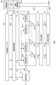
データ受信回路100は、遅延回路(データ遅延部)110と、出力バッファー120と、取込タイミング生成回路(取込タイミング生成部)130と、データ取込回路(データ取込部)140と、パルス幅検出回路(受信データ検出部)150とを備えている。また、データ受信回路100は、遅延制御レジスター160と、遅延制御回路180とを備えている。
The data receiving circuit 100 includes a delay circuit (data delay unit) 110, an output buffer 120, a capture timing generation circuit (capture timing generation unit) 130, a data capture circuit (data capture unit) 140, a pulse A width detection circuit (reception data detection unit) 150. Further, the data receiving circuit 100 includes a delay control register 160 and a delay control circuit 180.
遅延回路110は、表示データ供給装置20からの受信データDを遅延させる。遅延回路110は、1又は複数の遅延素子の各々が縦続に接続される構成を有し、各遅延素子の電源電圧の変更が可能に構成されている。従って、遅延回路110の電源電圧を高く設定することで受信データDの変化点のエッジを急峻にすることができ、遅延回路110の電源電圧を低く設定することで、受信データDの変化点のエッジを鈍化させることができる。
The delay circuit 110 delays the reception data D from the display data supply device 20. The delay circuit 110 has a configuration in which one or a plurality of delay elements are connected in cascade, and is configured such that the power supply voltage of each delay element can be changed. Therefore, the edge of the change point of the reception data D can be made sharp by setting the power supply voltage of the delay circuit 110 high, and the change point of the reception data D can be set by setting the power supply voltage of the delay circuit 110 low. Edges can be blunted.
出力バッファー120は、遅延回路110と取込タイミング生成回路130との間に設けられ、遅延回路110の出力をバッファリングして、取込タイミング生成回路130に、バッファリングした受信データを出力する。出力バッファー120の電源電圧は、変更可能に構成されている。従って、出力バッファー120の電源電圧を高く設定することで、受信データの変化点のエッジを急峻にすることができ、出力バッファー120の電源電圧を低く設定することで、受信データの変化点のエッジを鈍化させることができる。
The output buffer 120 is provided between the delay circuit 110 and the capture timing generation circuit 130, buffers the output of the delay circuit 110, and outputs the buffered reception data to the capture timing generation circuit 130. The power supply voltage of the output buffer 120 can be changed. Therefore, by setting the power supply voltage of the output buffer 120 high, the edge of the change point of the reception data can be made sharp, and by setting the power supply voltage of the output buffer 120 low, the edge of the change point of the reception data Can be slowed down.
取込タイミング生成回路130は、出力バッファー120(又は遅延回路110)の出力を順次遅延させて2種類以上の刻み幅を有する複数の取込タイミングを生成する。複数の取込タイミングは、基準タイミングに近い取込タイミングほど刻み幅が小さい。取込タイミング生成回路130は、複数の遅延回路DC0~DC19と、終端回路132と、複数のクロックバッファーCB0~CB19とを備えている。
The capture timing generation circuit 130 sequentially delays the output of the output buffer 120 (or the delay circuit 110) to generate a plurality of capture timings having two or more types of step sizes. The plurality of capture timings have smaller increments as the capture timing is closer to the reference timing. The capture timing generation circuit 130 includes a plurality of delay circuits DC0 to DC19, a termination circuit 132, and a plurality of clock buffers CB0 to CB19.
遅延回路DC0の入力には、出力バッファー120の出力が接続され、遅延回路DC0~DC19の各々が縦続に接続され、各遅延回路の出力が、各取込タイミングとなる。縦続に接続される遅延回路DC0~DC19の最終段の遅延回路DC19の出力には、終端回路132が接続される。遅延回路DC0~DC19の遅延値は、調整可能に構成されている。終端回路132の容量値は、調整可能に構成されている。終端回路132は、遅延回路DC0~DC19を伝搬する信号の反射を吸収する機能を有しており、その容量値を変更することで、各取込タイミングの遅延値も調整することができる。
The output of the output buffer 120 is connected to the input of the delay circuit DC0, each of the delay circuits DC0 to DC19 is connected in cascade, and the output of each delay circuit becomes each capture timing. A termination circuit 132 is connected to the output of the delay circuit DC19 at the final stage of the delay circuits DC0 to DC19 connected in cascade. The delay values of the delay circuits DC0 to DC19 are configured to be adjustable. The capacitance value of the termination circuit 132 is configured to be adjustable. The termination circuit 132 has a function of absorbing reflection of signals propagating through the delay circuits DC0 to DC19, and the delay value of each capture timing can be adjusted by changing the capacitance value.
複数のクロックバッファーCB0~CB19の各々の入力は、対応する遅延回路の出力に接続され、複数のクロックバッファーCB0~CB19の各々は、取込タイミングに対応する取込クロックCL0~CL19をデータ取込回路140に出力する。複数のクロックバッファーCB0~CB19の各々の電源電圧は、変更可能に構成されている。従って、クロックバッファーCB0~CB19の電源電圧を高く設定することで、取込クロックCL0~CL19の変化点のエッジを急峻にすることができる。クロックバッファーCB0~CB19の電源電圧を低く設定することで、取込クロックCL0~CL19の変化点のエッジを鈍化させることができる。
Each input of the plurality of clock buffers CB0 to CB19 is connected to the output of the corresponding delay circuit, and each of the plurality of clock buffers CB0 to CB19 captures the capture clocks CL0 to CL19 corresponding to the capture timing. Output to circuit 140. Each power supply voltage of the plurality of clock buffers CB0 to CB19 can be changed. Therefore, by setting the power supply voltage of the clock buffers CB0 to CB19 high, the edges of the transition points of the fetch clocks CL0 to CL19 can be made steep. By setting the power supply voltage of the clock buffers CB0 to CB19 low, the edges of the transition points of the fetch clocks CL0 to CL19 can be blunted.
データ取込回路140は、取込タイミング生成回路130によって生成された複数の取込タイミングで、所定のデータを取り込む。即ち、データ取込回路140は、複数の取込タイミングの各々に対応して設けられる複数のフリップフロップを備え、各フリップフロップが、対応する取込タイミングで変化する取込クロックに基づいて、所定のデータを取り込む。なお、各フリップフロップは、受信データDの受信に先立って初期化される。例えば、所定のデータは、Hレベルデータであり、初期化後のフリップフロップは、Lレベルデータを保持する。こうすることで、データ取込回路140は、取込クロックCL0~CL19のうちHレベルに変化する取込クロックが入力されるフリップフロップのみHレベルデータが保持される。Lレベルのままの取込クロックが入力されるフリップフロップは、Lレベルデータを保持するままである。データ取込回路140に取り込まれた取込データDL0~DL19は、パルス幅検出回路150に出力される。
The data capture circuit 140 captures predetermined data at a plurality of capture timings generated by the capture timing generation circuit 130. That is, the data capture circuit 140 includes a plurality of flip-flops provided corresponding to each of a plurality of capture timings, and each flip-flop is predetermined based on a capture clock that changes at the corresponding capture timing. Import the data. Each flip-flop is initialized prior to reception of reception data D. For example, the predetermined data is H level data, and the flip-flop after initialization holds L level data. By doing so, the data fetch circuit 140 holds the H level data only in the flip-flops to which the fetch clock that changes to the H level among the fetch clocks CL0 to CL19 is input. The flip-flop to which the capture clock that remains at the L level is input retains the L level data. Captured data DL0 to DL19 captured by the data capture circuit 140 is output to the pulse width detection circuit 150.
パルス幅検出回路150は、取込データDL0~DL19に基づいて受信データを検出する。具体的には、パルス幅検出回路150は、取込データDL1~DL16に基づいてパルス幅を検出することで、検出したパルス幅に対応した受信データを検出し、取込データDL0,DL17に基づいて、エラーを検出して、エラー検出結果信号ERRを出力する。パルス幅検出回路150において検出された受信データRDは、表示ドライバー30の駆動回路32に供給される。
The pulse width detection circuit 150 detects received data based on the acquired data DL0 to DL19. Specifically, the pulse width detection circuit 150 detects the received data corresponding to the detected pulse width by detecting the pulse width based on the captured data DL1 to DL16, and based on the captured data DL0 and DL17. An error is detected and an error detection result signal ERR is output. The reception data RD detected by the pulse width detection circuit 150 is supplied to the drive circuit 32 of the display driver 30.
遅延制御レジスター160には、遅延回路110、出力バッファー120、取込タイミング生成回路130を構成する遅延回路DC0~DC19、クロックバッファーCB0~CB19、及び終端回路132の少なくとも1つを制御するための制御値が設定される。
The delay control register 160 includes a control for controlling at least one of the delay circuit 110, the output buffer 120, the delay circuits DC0 to DC19, the clock buffers CB0 to CB19, and the termination circuit 132 that constitute the capture timing generation circuit 130. Value is set.
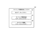
図4に、遅延制御レジスター160の構成の概要を示す。遅延制御レジスター160は、表示データ供給装置20又は図示しないCPU(以下、表示データ供給装置20等)によりアクセスが可能に構成されるレジスターである。
FIG. 4 shows an outline of the configuration of the delay control register 160. The delay control register 160 is a register that can be accessed by the display data supply device 20 or a CPU (not shown) (hereinafter, the display data supply device 20 or the like).
遅延制御レジスター160は、遅延回路制御レジスター162と、出力バッファー制御レジスター164と、容量値制御レジスター166と、クロックバッファー制御レジスター168と、終端回路制御レジスター170とを備えている。
The delay control register 160 includes a delay circuit control register 162, an output buffer control register 164, a capacitance value control register 166, a clock buffer control register 168, and a termination circuit control register 170.
遅延回路制御レジスター162には、第1の遅延設定レジスターとして、表示データ供給装置20等により、遅延回路110の電源電圧に対応した制御値が設定される。遅延制御回路180は、遅延回路制御レジスター162に設定された制御値に対応した制御信号C1を出力し、遅延回路110の電源電圧を該制御値に対応した電圧に設定する。
In the delay circuit control register 162, a control value corresponding to the power supply voltage of the delay circuit 110 is set as a first delay setting register by the display data supply device 20 or the like. The delay control circuit 180 outputs a control signal C1 corresponding to the control value set in the delay circuit control register 162, and sets the power supply voltage of the delay circuit 110 to a voltage corresponding to the control value.
出力バッファー制御レジスター164には、第2の遅延設定レジスターとして、表示データ供給装置20等により、出力バッファー120の電源電圧に対応した制御値が設定される。遅延制御回路180は、出力バッファー制御レジスター164に設定された制御値に対応した制御信号C2を出力し、出力バッファー120の電源電圧を該制御値に対応した電圧に設定する。
In the output buffer control register 164, a control value corresponding to the power supply voltage of the output buffer 120 is set as the second delay setting register by the display data supply device 20 or the like. The delay control circuit 180 outputs a control signal C2 corresponding to the control value set in the output buffer control register 164, and sets the power supply voltage of the output buffer 120 to a voltage corresponding to the control value.
このように遅延回路110及び出力バッファー120の各々に対して、独立に遅延値の調整ができるように構成している。これにより、例えば遅延回路110により大きく遅延値を調整し、出力バッファー120により十分な振幅レベルの受信データを、取込タイミング生成回路130に供給することができる。
As described above, the delay value can be independently adjusted for each of the delay circuit 110 and the output buffer 120. Thereby, for example, the delay value can be adjusted largely by the delay circuit 110, and the reception data having a sufficient amplitude level can be supplied to the capture timing generation circuit 130 by the output buffer 120.
容量値制御レジスター166には、第5の遅延設定レジスターとして、表示データ供給装置20等により、遅延回路DC0~DC19の遅延値に対応した制御値が設定される。具体的には、容量値制御レジスター166には、遅延回路DC0~DC19の各々を構成する容量素子の容量値に対応した制御値が設定される。遅延制御回路180は、容量値制御レジスター166に設定された制御値に対応した制御信号C3を出力し、遅延回路DC0~DC19の各々を構成する容量値を該制御値に対応した容量値に一斉に設定する。
In the capacitance value control register 166, a control value corresponding to the delay values of the delay circuits DC0 to DC19 is set as the fifth delay setting register by the display data supply device 20 or the like. Specifically, the capacitance value control register 166 is set with a control value corresponding to the capacitance value of the capacitive element constituting each of the delay circuits DC0 to DC19. The delay control circuit 180 outputs a control signal C3 corresponding to the control value set in the capacitance value control register 166, and simultaneously sets the capacitance value constituting each of the delay circuits DC0 to DC19 to the capacitance value corresponding to the control value. Set to.
クロックバッファー制御レジスター168には、第3の遅延設定レジスターとして、表示データ供給装置20等により、クロックバッファーCB0~CB19の電源電圧に対応した制御値が設定される。遅延制御回路180は、クロックバッファー制御レジスター168に設定された制御値に対応した制御信号C4を出力し、クロックバッファーCB0~CB19の電源電圧を該制御値に対応した電圧に一斉に設定する。
In the clock buffer control register 168, a control value corresponding to the power supply voltage of the clock buffers CB0 to CB19 is set as a third delay setting register by the display data supply device 20 or the like. The delay control circuit 180 outputs a control signal C4 corresponding to the control value set in the clock buffer control register 168, and simultaneously sets the power supply voltages of the clock buffers CB0 to CB19 to voltages corresponding to the control value.
終端回路制御レジスター170には、第4の遅延設定レジスターとして、表示データ供給装置20等により、終端回路132の容量値に対応した制御値が設定される。遅延制御回路180は、終端回路制御レジスター170に設定された制御値に対応した制御信号C5を出力し、終端回路132の容量値を該制御値に対応した容量値に設定する。
In the termination circuit control register 170, a control value corresponding to the capacitance value of the termination circuit 132 is set as the fourth delay setting register by the display data supply device 20 or the like. The delay control circuit 180 outputs a control signal C5 corresponding to the control value set in the termination circuit control register 170, and sets the capacitance value of the termination circuit 132 to a capacitance value corresponding to the control value.
以上のように、第1の実施形態におけるパルス幅変調では、受信データの立ち上がりが基準タイミングとして抽出される。この基準タイミングは、遅延回路110、出力バッファー120、複数の遅延回路DC0~DC19、クロックバッファーCB0~CB19及び終端回路132により順次遅延され、取込タイミングに対応した取込クロックとして生成される。遅延回路110、出力バッファー120、複数の遅延回路DC0~DC19、クロックバッファーCB0~CB19、及び終端回路132の各々は、遅延値の調整が可能に構成されている。そのため、取込タイミング、及びこれに対応した取込クロックを調整することができる。
As described above, in the pulse width modulation in the first embodiment, the rising edge of the received data is extracted as the reference timing. The reference timing is sequentially delayed by the delay circuit 110, the output buffer 120, the plurality of delay circuits DC0 to DC19, the clock buffers CB0 to CB19, and the termination circuit 132, and is generated as a capture clock corresponding to the capture timing. Each of the delay circuit 110, the output buffer 120, the plurality of delay circuits DC0 to DC19, the clock buffers CB0 to CB19, and the termination circuit 132 is configured to be able to adjust the delay value. Therefore, the capture timing and the capture clock corresponding to this can be adjusted.
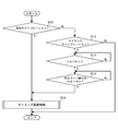
図5に、第1の実施形態におけるデータ受信回路100の動作例のフロー図を示す。
FIG. 5 shows a flowchart of an operation example of the data receiving circuit 100 according to the first embodiment.
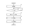
まず、データ受信回路100は、表示データ供給装置20等により、遅延制御レジスター160を構成する各レジスターに制御値が設定され、遅延値が調整される(ステップS1、遅延調整ステップ)。例えば、表示データ供給装置20等が、各レジスターに制御値を設定してパルス幅検出回路150の検出結果を検定することを繰り返す。この結果、遅延回路110、出力バッファー120、遅延回路DC0~DC19、クロックバッファーCB0~CB19及び終端回路132の各々の最適な遅延値が決定される。
First, in the data receiving circuit 100, the display data supply device 20 or the like sets a control value in each register constituting the delay control register 160 and adjusts the delay value (step S1, delay adjustment step). For example, the display data supply device 20 or the like repeatedly sets the control value in each register and verifies the detection result of the pulse width detection circuit 150. As a result, the optimum delay values of the delay circuit 110, the output buffer 120, the delay circuits DC0 to DC19, the clock buffers CB0 to CB19, and the termination circuit 132 are determined.
次に、データ受信回路100は、表示データ供給装置20からのデータ受信を待つ(ステップS2:N)。
Next, the data receiving circuit 100 waits for data reception from the display data supply device 20 (step S2: N).
表示データ供給装置20からのデータが受信されたとき(ステップS2:Y)、データ受信回路100は、出力バッファー120を介して入力された受信データに基づき、取込タイミングを生成する(ステップS3、取込タイミング生成ステップ)。具体的には、データ受信回路100は、取込タイミング生成回路130において、受信データの立ち上がりタイミングを順次遅延させることで、取込タイミングを生成する。このとき、取込タイミング生成回路130は、取込タイミングに対応した取込クロックCL0~CL19を、データ取込回路140に出力する。
When data from the display data supply device 20 is received (step S2: Y), the data reception circuit 100 generates a capture timing based on the received data input via the output buffer 120 (step S3, Capture timing generation step). Specifically, the data reception circuit 100 generates the capture timing by sequentially delaying the rising timing of the received data in the capture timing generation circuit 130. At this time, the capture timing generation circuit 130 outputs capture clocks CL0 to CL19 corresponding to the capture timing to the data capture circuit 140.
続いて、データ受信回路100は、データ取込回路140を構成する複数のフリップフロップにおいて、取込クロックCL0~CL19に基づいてHレベルデータを取り込む(ステップS4、データ取込ステップ)。データ取込回路140は、複数のフリップフロップにラッチされたデータを取込データDL0~DL19として、パルス幅検出回路150に出力する。
Subsequently, the data receiving circuit 100 takes in the H level data based on the take-in clocks CL0 to CL19 in the plurality of flip-flops constituting the data take-in circuit 140 (step S4, data take-in step). The data acquisition circuit 140 outputs the data latched by the plurality of flip-flops to the pulse width detection circuit 150 as the acquisition data DL0 to DL19.
その後、データ受信回路100は、パルス幅検出回路150において、データ取込回路140により複数の取込タイミングで取り込まれた取込データDL0~DL19に基づいて受信データを検出する(ステップS5、受信データ検出ステップ)。その後、データ受信回路100は、一連の処理を終了する(エンド)。
Thereafter, the data receiving circuit 100 detects the received data in the pulse width detection circuit 150 based on the acquired data DL0 to DL19 acquired by the data acquiring circuit 140 at a plurality of acquisition timings (step S5, received data). Detection step). Thereafter, the data receiving circuit 100 ends a series of processing (end).
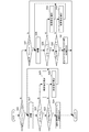
図6に、図3のデータ受信回路100の詳細な構成例の回路図を示す。なお、図6では、図3のパルス幅検出回路150、遅延制御レジスター160、及び遅延制御回路180の図示を省略している。図6において、図3と同様の部分には同一符号を付し、適宜説明を省略する。
FIG. 6 shows a circuit diagram of a detailed configuration example of the data receiving circuit 100 of FIG. In FIG. 6, the pulse width detection circuit 150, the delay control register 160, and the delay control circuit 180 in FIG. 3 are not shown. 6, parts that are the same as those in FIG. 3 are given the same reference numerals, and descriptions thereof are omitted as appropriate.
遅延回路110は、縦続に接続される複数のバッファーを備えており、各バッファーの電源電圧が制御信号C1により設定される電圧に設定される。
The delay circuit 110 includes a plurality of buffers connected in cascade, and the power supply voltage of each buffer is set to a voltage set by the control signal C1.
取込タイミング生成回路130は、遅延回路DC0~DC19、終端回路132、及びクロックバッファーCB0~CB19に加えて、容量初期化回路134を備えている。
The capture timing generation circuit 130 includes a capacity initialization circuit 134 in addition to the delay circuits DC0 to DC19, the termination circuit 132, and the clock buffers CB0 to CB19.
遅延回路DC0は、一端が出力バッファー120の出力に接続され他端が容量素子の一方の電極と接続される抵抗素子と、他方の電極が接地される該容量素子とを備えている。この抵抗素子の他端が、次段の遅延回路DC1に接続されると共に、対応するクロックバッファーCB0の入力に接続される。遅延回路DC0を構成する容量素子は、バラクタダイオードであり、アノードとカソードとの間に印加する逆バイアス電圧により接合容量が変化ことで容量値が可変な素子である。この容量素子の容量値は、制御信号C3により設定される。遅延回路DC0~DC19の各々は、同様の構成を有している。
The delay circuit DC0 includes a resistance element having one end connected to the output of the output buffer 120 and the other end connected to one electrode of the capacitor, and the capacitor having the other electrode grounded. The other end of this resistance element is connected to the delay circuit DC1 at the next stage and to the input of the corresponding clock buffer CB0. The capacitive element constituting the delay circuit DC0 is a varactor diode, and is an element whose capacitance value is variable by changing the junction capacitance by a reverse bias voltage applied between the anode and the cathode. The capacitance value of this capacitive element is set by the control signal C3. Each of the delay circuits DC0 to DC19 has the same configuration.
終端回路132は、一端が遅延回路DC19の出力に接続され他端が容量素子の一方の電極と接続される抵抗素子と、他方の電極が接地される該容量素子とを備えている。この容量素子は、バラクタダイオードであり、その容量値は、制御信号C5により設定される。
The termination circuit 132 includes a resistive element having one end connected to the output of the delay circuit DC19 and the other end connected to one electrode of the capacitive element, and the capacitive element having the other electrode grounded. This capacitive element is a varactor diode, and its capacitance value is set by a control signal C5.
容量初期化回路134は、取込タイミング生成回路130による各取込タイミングの出力に先立って、遅延回路DC0~DC19の各々を構成する容量素子に充電された電荷を初期化する。このような容量初期化回路134は、遅延回路DC0~DC19の各々を構成する容量素子に対応して設けられた複数のN型MOSFET(Metal-Oxide-Semiconductor Field-Effect Transistor)を備えている。各MOSFETのソースは接地され、ドレインは、対応する遅延回路を構成する容量素子の一方の電極が接続される。各MOSFETのゲートには、遅延回路110の出力を論理反転した信号が供給され、受信データDの立ち上がりタイミング以前のLレベルのとき、MOSFETがオンするようになっている。これにより、遅延回路DC0~DC19は、受信データが繰り返し入力された場合であっても、取込タイミングを精度良く遅延させることができるようになる。
Capacitance initialization circuit 134 initializes the charges charged in the capacitive elements constituting each of delay circuits DC0 to DC19 prior to the output of each capture timing by capture timing generation circuit 130. Such a capacitance initialization circuit 134 includes a plurality of N-type MOSFETs (Metal-Oxide-Semiconductor Field-Effect Transistors) provided corresponding to the capacitance elements constituting each of the delay circuits DC0 to DC19. The source of each MOSFET is grounded, and the drain is connected to one electrode of the capacitive element constituting the corresponding delay circuit. A signal obtained by logically inverting the output of the delay circuit 110 is supplied to the gate of each MOSFET, and the MOSFET is turned on at the L level before the rising timing of the reception data D. As a result, the delay circuits DC0 to DC19 can delay the capture timing with high accuracy even when received data is repeatedly input.
データ取込回路140は、フリップフロップDF0~DF19を備えている。フリップフロップDF0~DF19の各々は、データ入力端子Dと、クロック入力端子Cと、データ出力端子Qと、リセット入力端子Rとを備えている。フリップフロップDF0~DF19の各々のクロック入力端子Cには、対応するクロックバッファーからの取込クロックが入力される。フリップフロップDF0~DF19の各々のデータ入力端子Dには、高電位側電源が接続される。フリップフロップDF0~DF19の各々は、クロック入力端子Cに入力される信号の立ち上がりで、データ入力端子Dに入力されるHレベルデータを取り込み、取り込んだデータをデータ出力端子Qから取込データとして出力する。フリップフロップDF0~DF19のデータ出力端子Qから取込データDL0~DL19が出力される。
The data fetch circuit 140 includes flip-flops DF0 to DF19. Each of the flip-flops DF0 to DF19 includes a data input terminal D, a clock input terminal C, a data output terminal Q, and a reset input terminal R. The clock input terminal C of each of the flip-flops DF0 to DF19 is input with a clock taken in from the corresponding clock buffer. A high potential power source is connected to each data input terminal D of the flip-flops DF0 to DF19. Each of the flip-flops DF0 to DF19 takes in the H level data inputted to the data input terminal D at the rising edge of the signal inputted to the clock input terminal C, and outputs the taken data from the data output terminal Q as taken data. To do. Captured data DL0 to DL19 are output from data output terminals Q of flip-flops DF0 to DF19.
また、フリップフロップDF0~DF19の各々のリセット入力端子Rには、リセット回路142により生成されたリセット信号が入力される。リセット回路142は、立ち上がり検出回路であり、受信データDの立ち上がりタイミングに同期して、Lレベルに変化するパルス信号を出力する。従って、フリップフロップDF0~DF19は、受信データDの立ち上がりタイミングで、初期化される。
Also, the reset signal generated by the reset circuit 142 is input to the reset input terminals R of the flip-flops DF0 to DF19. The reset circuit 142 is a rise detection circuit, and outputs a pulse signal that changes to the L level in synchronization with the rise timing of the reception data D. Accordingly, the flip-flops DF0 to DF19 are initialized at the rising timing of the reception data D.
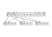
図7に、図3のパルス幅検出回路150の構成例の回路図を示す。図7において、図3と同様の部分には同一符号を付し、適宜説明を省略する。
FIG. 7 shows a circuit diagram of a configuration example of the pulse width detection circuit 150 of FIG. 7, parts that are the same as those in FIG. 3 are given the same reference numerals, and explanation thereof is omitted as appropriate.
図7のパルス幅検出回路150は、取込データDL0,DL17に基づいて、エラーを検出して、エラー検出結果信号ERRを出力する。取込データDL0,DL17は、4ビットの表示データをパルス幅変調したデータに対応した取込データDL1~DL16の前後の状態を表す。エラー検出結果信号ERRは、取込データDL0に基づいて、表示データ「(0)16」(=(0000)2)がパルス幅変調されたデータよりもパルス幅が小さいときにHレベルに変化する。また、エラー検出結果信号ERRは、取込データDL17に基づいて、表示データ「(F)16」(=(1111)2)がパルス幅変調されたデータよりもパルス幅が大きいときにHレベルに変化する。
The pulse width detection circuit 150 in FIG. 7 detects an error based on the captured data DL0 and DL17 and outputs an error detection result signal ERR. Captured data DL0 and DL17 represent states before and after captured data DL1 to DL16 corresponding to data obtained by pulse width modulation of 4-bit display data. The error detection result signal ERR changes to the H level when the display data “(0) 16 ” (= (0000) 2 ) has a pulse width smaller than the pulse width modulated data, based on the captured data DL0. . Further, the error detection result signal ERR is set to the H level when the display data “(F) 16 ” (= (1111) 2 ) has a pulse width larger than the pulse width modulated data based on the captured data DL17. Change.
また、パルス幅検出回路150は、上位ビットデコーダー152を備えている。パルス幅検出回路150は、取込データDL1~DL16の取込データDL1,DL2,DL3,・・・,DL16の順番に排他的論理和演算することにより、4ビットの受信データの最下位ビットRD<0>を生成する。また、上位ビットデコーダー152は、取込データDL2~DL16をデコードすることで、4ビットの受信データの上位ビットRD<3:1>の各ビットを生成する。こうしてパルス幅検出回路150において検出された受信データRD<3:0>は、表示ドライバー30の駆動回路32に供給される。
In addition, the pulse width detection circuit 150 includes an upper bit decoder 152. The pulse width detection circuit 150 performs an exclusive OR operation in the order of the acquisition data DL1, DL2, DL3,..., DL16 of the acquisition data DL1 to DL16 to thereby obtain the least significant bit RD of the 4-bit reception data. <0> is generated. Further, the upper bit decoder 152 generates each bit of the upper bits RD <3: 1> of the received data of 4 bits by decoding the fetched data DL2 to DL16. The reception data RD <3: 0> detected by the pulse width detection circuit 150 in this way is supplied to the drive circuit 32 of the display driver 30.
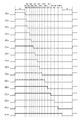
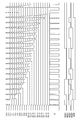
図8に、第1の実施形態におけるデータ受信回路100のシミュレーション結果の一例を示す。図8は、横軸に時間軸をとり、受信データD、取込データDL0~DL19、検出された受信データRD<3>~RD<0>、エラー検出結果信号ERRを表す。なお、図8は、第1の実施形態の特有の動作を説明するために、受信データDのパルス幅を1サイクル毎に0.5nsずつ長くして、取込データDL0~DL19、受信データRD<3>~RD<0>、エラー検出結果信号ERRの変化を表したものである。
FIG. 8 shows an example of a simulation result of the data receiving circuit 100 according to the first embodiment. FIG. 8 shows the received data D, the captured data DL0 to DL19, the detected received data RD <3> to RD <0>, and the error detection result signal ERR, with the time axis on the horizontal axis. In FIG. 8, in order to explain operations peculiar to the first embodiment, the pulse width of the reception data D is increased by 0.5 ns for each cycle, and the acquisition data DL0 to DL19 and reception data RD are increased. <3> to RD <0> represent changes in the error detection result signal ERR.
図2と異なり、立ち下がりエッジの位置を均等に規定した場合、受信データDのパルス幅を1サイクル毎に所定の長さだけ長くしていくと、パルス幅検出回路150において検出される受信データRD<3:0>の値は、ある一定の割合で増加していく。
Unlike FIG. 2, when the positions of the falling edges are uniformly defined, the reception data detected by the pulse width detection circuit 150 is increased when the pulse width of the reception data D is increased by a predetermined length every cycle. The value of RD <3: 0> increases at a certain rate.
これに対して、第1の実施形態では、基準タイミングに近いほど刻み幅を小さくし、基準タイミングから遠いほど刻み幅を大きくしている。従って、受信データDのパルス幅を1サイクル毎に所定の長さだけ長くしていくと、パルス幅検出回路150において検出される受信データRD<3:0>の値は、パルス幅が小さい場合に比べてパルス幅が大きい場合には増加しにくくなっている。
On the other hand, in the first embodiment, the step size is reduced as it is closer to the reference timing, and the step size is increased as it is farther from the reference timing. Accordingly, when the pulse width of the reception data D is increased by a predetermined length for each cycle, the value of the reception data RD <3: 0> detected by the pulse width detection circuit 150 is the case where the pulse width is small. When the pulse width is large compared to the above, it is difficult to increase.
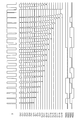
図9に、第1の実施形態におけるデータ受信回路100のシミュレーション結果の他の例を示す。図9は、横軸に時間軸をとり、受信データD、取込クロックCL0~CL19、及び検出された受信データRD<3>~RD<0>を表す。なお、図9は、図8と同一の時間軸であり、図8と同様に、受信データDのパルス幅を1サイクル毎に0.5nsずつ長くして、取込クロックCL0~CL19、受信データRD<3>~RD<0>の変化を表したものである。
FIG. 9 shows another example of the simulation result of the data receiving circuit 100 in the first embodiment. FIG. 9 shows the reception data D, the acquisition clocks CL0 to CL19, and the detected reception data RD <3> to RD <0> with the time axis on the horizontal axis. FIG. 9 is the same time axis as FIG. 8. Like FIG. 8, the pulse width of the reception data D is increased by 0.5 ns per cycle, and the acquisition clocks CL0 to CL19, reception data This represents a change in RD <3> to RD <0>.
図8において説明したように、立ち下がりエッジの位置を均等に規定した場合、受信データDのパルス幅を1サイクル毎に所定の長さだけ長くしていくと、取込クロックCL0~CL19は、一定の割合でHレベルに変化していく。こうすることで、データ取込回路140を構成する複数のフリップフロップは、対応する取込クロックがHレベルに変化することによりHレベルデータを取り込むことができる。
As described in FIG. 8, when the positions of the falling edges are uniformly defined, if the pulse width of the reception data D is increased by a predetermined length every cycle, the acquisition clocks CL0 to CL19 are It changes to H level at a constant rate. By doing so, the plurality of flip-flops constituting the data capture circuit 140 can capture the H level data when the corresponding capture clock changes to the H level.
これに対して、第1の実施形態では、基準タイミングに近いほど刻み幅を小さくし、基準タイミングから遠いほど刻み幅を大きくしている。従って、受信データDのパルス幅を1サイクル毎に所定の長さだけ長くしていくと、取込クロックCL0~CL19は、一定の割合でHレベルに変化しない。図9に示すように、データ取込回路140を構成する複数のフリップフロップのうち、十分にHレベルに立ち上がることができない取込クロックが入力されるフリップフロップは、Hレベルデータを取り込むことができない。この結果、パルス幅が小さい場合に比べてパルス幅が大きい場合には、パルス幅検出回路150において検出される受信データRD<3:0>の値が増加しにくくなっている。
On the other hand, in the first embodiment, the step size is reduced as it is closer to the reference timing, and the step size is increased as it is farther from the reference timing. Therefore, when the pulse width of the reception data D is increased by a predetermined length every cycle, the acquisition clocks CL0 to CL19 do not change to the H level at a constant rate. As shown in FIG. 9, among a plurality of flip-flops constituting data fetch circuit 140, a flip-flop to which a fetch clock that cannot sufficiently rise to H level is input cannot fetch H level data. . As a result, when the pulse width is larger than when the pulse width is small, the value of the reception data RD <3: 0> detected by the pulse width detection circuit 150 is difficult to increase.
以上説明したように、第1の実施形態においては、基準タイミングから遠いほど刻み幅が粗くなるように各立ち下がりエッジの位置が規定されるパルス幅変調により、表示データを受信するようにした。これにより、基準タイミングに近い立ち下がりエッジの位置については、正確に規定することができる。一方、基準タイミングから遠い立ち下がりエッジの位置については、刻み幅が大きいため、素子ばらつきがあっても、立ち下がりエッジの位置を精度良く規定することができる。
As described above, in the first embodiment, display data is received by pulse width modulation in which the position of each falling edge is defined so that the step width becomes coarser as the distance from the reference timing increases. Thereby, the position of the falling edge close to the reference timing can be accurately defined. On the other hand, the position of the falling edge far from the reference timing has a large step size, so that the position of the falling edge can be accurately defined even if there is element variation.
この結果、受信データから抽出される基準タイミングを順次遅延させて、各立ち下がりエッジの取込タイミングを生成することができるので、PLL回路を設けることなく、立ち下がりエッジの位置を精度良く規定することができる。この結果、パルス幅変調の多ビット化を実現し、測定機器の測定限界を超えた周波数であっても、低コストで、大容量の表示データを高速に送受信することができるようになる。
As a result, the reference timing extracted from the received data can be sequentially delayed to generate the capture timing of each falling edge, so that the position of the falling edge can be accurately defined without providing a PLL circuit. be able to. As a result, it is possible to increase the number of bits of pulse width modulation, and to transmit and receive large-capacity display data at high speed at low cost even at a frequency exceeding the measurement limit of the measuring device.
〔第2の実施形態〕
第1の実施形態では、表示データ供給装置20等により、遅延回路110、出力バッファー120、複数の遅延回路DC0~DC19、クロックバッファーCB0~CB19、及び終端回路132の各々の最適な遅延値を決定するものとして説明した。しかしながら、本発明に係る実施形態は、これに限定されるものではない。 [Second Embodiment]
In the first embodiment, the displaydata supply device 20 or the like determines the optimum delay value of each of the delay circuit 110, the output buffer 120, the plurality of delay circuits DC0 to DC19, the clock buffers CB0 to CB19, and the termination circuit 132. Explained as what to do. However, the embodiment according to the present invention is not limited to this.
第1の実施形態では、表示データ供給装置20等により、遅延回路110、出力バッファー120、複数の遅延回路DC0~DC19、クロックバッファーCB0~CB19、及び終端回路132の各々の最適な遅延値を決定するものとして説明した。しかしながら、本発明に係る実施形態は、これに限定されるものではない。 [Second Embodiment]
In the first embodiment, the display
図10に、本発明の第2の実施形態におけるデータ受信回路の構成例のブロック図を示す。なお、図10では、図3と同様に、パルス幅変調により4ビットの表示データが変調された受信データを受信する場合の構成例を表す。図10において、図3と同様の部分には同一符号を付し、適宜説明を省略する。
FIG. 10 is a block diagram showing a configuration example of the data receiving circuit according to the second embodiment of the present invention. 10 shows a configuration example in the case of receiving reception data in which 4-bit display data is modulated by pulse width modulation, as in FIG. 10, parts that are the same as those in FIG. 3 are given the same reference numerals, and descriptions thereof will be omitted as appropriate.
第2の実施形態におけるデータ受信回路100aは、遅延回路110と、出力バッファー120と、取込タイミング生成回路130と、データ取込回路140と、パルス幅検出回路150と、遅延制御レジスター160と、遅延制御回路180aとを備えている。また、データ受信回路100aは、タイミング調整制御レジスター190と、タイミング調整制御回路200とを備えている。図3に示すデータ受信回路100の構成が第2の実施形態におけるデータ受信回路100aの構成と異なる主な点は、タイミング調整制御レジスター190及びタイミング調整制御回路200が追加された点である。図1の表示ドライバー30におけるデータ受信回路100に代えて、このようなデータ受信回路100aを設けることができる。なお、データ受信回路100aを構成する回路のうち、図3と同様の回路については、図6又は図7に示した構成と同様に構成することができる。
The data receiving circuit 100a in the second embodiment includes a delay circuit 110, an output buffer 120, a capture timing generation circuit 130, a data capture circuit 140, a pulse width detection circuit 150, a delay control register 160, A delay control circuit 180a. The data receiving circuit 100a includes a timing adjustment control register 190 and a timing adjustment control circuit 200. The main difference between the configuration of the data receiving circuit 100 shown in FIG. 3 and the configuration of the data receiving circuit 100a in the second embodiment is that a timing adjustment control register 190 and a timing adjustment control circuit 200 are added. Such a data receiving circuit 100a can be provided in place of the data receiving circuit 100 in the display driver 30 of FIG. Of the circuits constituting the data receiving circuit 100a, circuits similar to those in FIG. 3 can be configured in the same manner as those shown in FIG. 6 or FIG.
タイミング調整制御レジスター190には、表示データ供給装置20等により、タイミング調整制御を行うための制御値が設定される。
In the timing adjustment control register 190, a control value for performing timing adjustment control is set by the display data supply device 20 or the like.
図11に、タイミング調整制御レジスター190の構成の概要を示す。タイミング調整制御レジスター190は、表示データ供給装置20等によりアクセスが可能に構成されるレジスターである。
FIG. 11 shows an outline of the configuration of the timing adjustment control register 190. The timing adjustment control register 190 is a register configured to be accessible by the display data supply device 20 or the like.
タイミング調整制御レジスター190は、出力データレジスター192と、タイミング調整強制イネーブルレジスター194と、タイミング調整イネーブルレジスター196とを備えている。
The timing adjustment control register 190 includes an output data register 192, a timing adjustment forced enable register 194, and a timing adjustment enable register 196.
出力データレジスター192には、表示データ供給装置20等により、表示データ供給装置20からデータ受信回路100aに送信されるデータの値が設定される。出力データレジスター192に「(0)16」が設定されたとき、「(0)16」値に対応した4ビットのデータがパルス幅変調されたデータがデータ受信回路100aにおいて受信される。また、出力データレジスター192に「(F)16」が設定されたとき、「(F)16」値に対応した4ビットのデータがパルス幅変調されたデータがデータ受信回路100aにおいて受信される。
In the output data register 192, the value of data transmitted from the display data supply device 20 to the data receiving circuit 100a is set by the display data supply device 20 or the like. When “(0) 16 ” is set in the output data register 192, the data receiving circuit 100a receives data obtained by pulse-width-modulating 4-bit data corresponding to the “(0) 16 ” value. When “(F) 16 ” is set in the output data register 192, data obtained by pulse width modulation of 4-bit data corresponding to the “(F) 16 ” value is received by the data receiving circuit 100 a.
タイミング調整強制イネーブルレジスター194には、表示データ供給装置20等により、強制的にタイミング調整制御を行うことを指示するイネーブルビットが設定される。タイミング調整強制イネーブルレジスター194にイネーブルビットが設定されたとき、データ受信回路100aは、出力データレジスター192に設定された値の取込タイミングを規定するための遅延値を調整する制御を強制的に行う。
In the timing adjustment forced enable register 194, an enable bit for instructing to perform timing adjustment control forcibly by the display data supply device 20 or the like is set. When the enable bit is set in the timing adjustment forced enable register 194, the data receiving circuit 100a forcibly performs control for adjusting the delay value for defining the timing of taking in the value set in the output data register 192. .
タイミング調整イネーブルレジスター196には、表示データ供給装置20等により、タイミング調整制御を行うことを指示するイネーブルビットが設定される。タイミング調整イネーブルレジスター196にイネーブルビットが設定されたとき、データ受信回路100aは、例えば帰線期間中に、出力データレジスター192に設定された値の取込タイミングを規定するための遅延値を調整する制御を行う。
In the timing adjustment enable register 196, an enable bit for instructing to perform timing adjustment control is set by the display data supply device 20 or the like. When the enable bit is set in the timing adjustment enable register 196, the data reception circuit 100a adjusts the delay value for defining the timing of taking in the value set in the output data register 192, for example, during the blanking period. Take control.
表示データ供給装置20等によりタイミング調整強制イネーブルレジスター194又はタイミング調整イネーブルレジスター196にイネーブルビットが設定されると、データ受信回路100aは、次のようなタイミング調整制御を行う。そして、タイミング調整制御の結果、遅延制御レジスター160には、最適な制御値が設定される。
When the enable bit is set in the timing adjustment forced enable register 194 or the timing adjustment enable register 196 by the display data supply device 20 or the like, the data receiving circuit 100a performs the following timing adjustment control. As a result of the timing adjustment control, an optimum control value is set in the delay control register 160.
図12及び図13に、第2の実施形態におけるタイミング調整制御の動作例のフロー図を示す。図13は、図12のステップS11において行われる動作例のフロー図を表す。なお、図12及び図13に示すフローは、図5の遅延調整ステップとしてのステップS1において行われることが望ましい。
FIG. 12 and FIG. 13 are flowcharts showing an operation example of the timing adjustment control in the second embodiment. FIG. 13 shows a flowchart of an operation example performed in step S11 of FIG. The flow shown in FIGS. 12 and 13 is desirably performed in step S1 as the delay adjustment step in FIG.
まず、データ受信回路100aは、タイミング調整制御回路200において、強制キャリブレーションの指示の有無を判定する(ステップS10)。具体体には、ステップS10において、タイミング調整制御回路200は、タイミング調整強制イネーブルレジスター194にイネーブルビットが設定されているか否かを判定する。タイミング調整強制イネーブルレジスター194にイネーブルビットが設定されているとき(ステップS10:Y)、タイミング調整制御回路200は、タイミング調整制御を行い(ステップS11)、一連の処理を終了する(エンド)。
First, the data receiving circuit 100a determines whether or not there is a forced calibration instruction in the timing adjustment control circuit 200 (step S10). Specifically, in step S10, the timing adjustment control circuit 200 determines whether or not an enable bit is set in the timing adjustment forced enable register 194. When the enable bit is set in the timing adjustment forced enable register 194 (step S10: Y), the timing adjustment control circuit 200 performs timing adjustment control (step S11), and ends a series of processing (end).
タイミング調整強制イネーブルレジスター194にイネーブルビットが設定されていないとき(ステップS10:N)、タイミング調整制御回路200は、タイミングキャリブレーションの指示の有無を判定する(ステップS12)。具体的には、ステップS12では、タイミング調整制御回路200は、タイミング調整イネーブルレジスター196にイネーブルビットが設定されているか否かを判定する。タイミング調整イネーブルレジスター196にイネーブルビットが設定されているとき(ステップS12:Y)、タイミング調整制御回路200は、帰線期間中に、タイミング調整制御を行う。即ち、タイミング調整制御回路200は、垂直同期信号VSYNCがアクティブになるまで待つ(ステップS13:N)。垂直同期信号VSYNCがアクティブになると(ステップS13:Y)、タイミング調整制御回路200は、所定ライン数分の水平同期信号HSYNCがアクティブになるまで待つ(ステップS14:N)。所定ライン数分の水平同期信号HSYNCがアクティブになったとき(ステップS14:Y)、タイミング調整制御回路200は、タイミング調整制御を行い(ステップS11)、一連の処理を終了する(エンド)。
When the enable bit is not set in the timing adjustment forced enable register 194 (step S10: N), the timing adjustment control circuit 200 determines whether or not there is a timing calibration instruction (step S12). Specifically, in step S12, the timing adjustment control circuit 200 determines whether an enable bit is set in the timing adjustment enable register 196. When the enable bit is set in the timing adjustment enable register 196 (step S12: Y), the timing adjustment control circuit 200 performs timing adjustment control during the blanking period. That is, the timing adjustment control circuit 200 waits until the vertical synchronization signal VSYNC becomes active (step S13: N). When the vertical synchronization signal VSYNC becomes active (step S13: Y), the timing adjustment control circuit 200 waits until the horizontal synchronization signal HSYNC for a predetermined number of lines becomes active (step S14: N). When the horizontal synchronization signals HSYNC for a predetermined number of lines become active (step S14: Y), the timing adjustment control circuit 200 performs timing adjustment control (step S11), and ends a series of processing (end).
ステップS11では、図13に示すように、タイミング調整制御回路200は、出力データレジスター192に設定された値が「(0)16」であるか否かを判定する(ステップS20)。出力データレジスター192に「(0)16」が設定されているとき(ステップS20:Y)、タイミング調整制御回路200は、所定の期間だけ待機する(ステップS21)。この所定の期間内に、表示データ供給装置20からパルス幅が最短のデータが送信され、データ受信回路100aのパルス幅検出回路150において受信データが検出される。
In step S11, as shown in FIG. 13, the timing adjustment control circuit 200 determines whether or not the value set in the output data register 192 is “(0) 16 ” (step S20). When “(0) 16 ” is set in the output data register 192 (step S20: Y), the timing adjustment control circuit 200 waits for a predetermined period (step S21). Within this predetermined period, data with the shortest pulse width is transmitted from the display data supply device 20, and the received data is detected by the pulse width detection circuit 150 of the data reception circuit 100a.
ステップS21に続いて、タイミング調整制御回路200は、パルス幅検出回路150からのエラー検出結果信号ERRに基づいて、エラーの有無を判定する(ステップS22)。エラー検出結果信号ERRに基づいてエラーがないと判定されたとき(ステップS22:Y)、タイミング調整制御回路200は、受信データRD<3:0>に基づいてパルス幅が「0」であるか否かを判定する(ステップS23)。パルス幅が「0」であるとき(ステップS23:Y)、タイミング調整制御回路200は、現在の遅延値に対応した制御値を、遅延回路制御レジスター162に設定し(ステップS24)、一連の処理を終了する(エンド)。
Subsequent to step S21, the timing adjustment control circuit 200 determines the presence or absence of an error based on the error detection result signal ERR from the pulse width detection circuit 150 (step S22). When it is determined that there is no error based on the error detection result signal ERR (step S22: Y), the timing adjustment control circuit 200 determines whether the pulse width is “0” based on the reception data RD <3: 0>. It is determined whether or not (step S23). When the pulse width is “0” (step S23: Y), the timing adjustment control circuit 200 sets a control value corresponding to the current delay value in the delay circuit control register 162 (step S24), and a series of processes End (end).
ステップS22においてエラー検出結果信号ERRに基づいてエラーがあると判定されたとき(ステップS22:N)、タイミング調整制御回路200は、遅延回路制御レジスター162に設定された制御値を増加させて(ステップS25)、ステップS21に戻る。
When it is determined in step S22 that there is an error based on the error detection result signal ERR (step S22: N), the timing adjustment control circuit 200 increases the control value set in the delay circuit control register 162 (step S22). S25), the process returns to step S21.
ステップS23においてパルス幅が「0」でないとき(ステップS23:N)、タイミング調整制御回路200は、遅延回路制御レジスター162に設定された制御値を減少させて(ステップS26)、ステップS21に戻る。
When the pulse width is not “0” in step S23 (step S23: N), the timing adjustment control circuit 200 decreases the control value set in the delay circuit control register 162 (step S26), and returns to step S21.
出力データレジスター192に「(0)16」が設定されていないとき(ステップS20:N)、タイミング調整制御回路200は、出力データレジスター192に設定された値が「(F)16」であるか否かを判定する(ステップS27)。
When “(0) 16 ” is not set in the output data register 192 (step S20: N), the timing adjustment control circuit 200 determines whether the value set in the output data register 192 is “(F) 16 ”. It is determined whether or not (step S27).
出力データレジスター192に「(F)16」が設定されているとき(ステップS27:Y)、タイミング調整制御回路200は、所定の期間だけ待機する(ステップS28)。この所定の期間内に、表示データ供給装置20からパルス幅が最長のデータが送信され、データ受信回路100aのパルス幅検出回路150において受信データが検出される。
When “(F) 16 ” is set in the output data register 192 (step S27: Y), the timing adjustment control circuit 200 waits for a predetermined period (step S28). Within this predetermined period, the data with the longest pulse width is transmitted from the display data supply device 20, and the received data is detected by the pulse width detection circuit 150 of the data reception circuit 100a.
ステップS28に続いて、タイミング調整制御回路200は、パルス幅検出回路150からのエラー検出結果信号ERRに基づいて、エラーの有無を判定する(ステップS29)。エラー検出結果信号ERRに基づいてエラーがないと判定されたとき(ステップS29:Y)、タイミング調整制御回路200は、受信データRD<3:0>に基づいてパルス幅が「15」であるか否かを判定する(ステップS30)。パルス幅が「15」であるとき(ステップS30:Y)、タイミング調整制御回路200は、現在の遅延値に対応した制御値を、出力バッファー制御レジスター164と、容量値制御レジスター166と、クロックバッファー制御レジスター168と、終端回路制御レジスター170に設定し(ステップS31)、一連の処理を終了する(エンド)。
Subsequent to step S28, the timing adjustment control circuit 200 determines the presence or absence of an error based on the error detection result signal ERR from the pulse width detection circuit 150 (step S29). When it is determined that there is no error based on the error detection result signal ERR (step S29: Y), the timing adjustment control circuit 200 determines whether the pulse width is “15” based on the reception data RD <3: 0>. It is determined whether or not (step S30). When the pulse width is “15” (step S30: Y), the timing adjustment control circuit 200 sets the control value corresponding to the current delay value to the output buffer control register 164, the capacitance value control register 166, and the clock buffer. The control register 168 and the termination circuit control register 170 are set (step S31), and the series of processing ends (end).
ステップS29においてエラー検出結果信号ERRに基づいてエラーがあると判定されたとき(ステップS29:N)、タイミング調整制御回路200は、出力バッファー制御レジスター164と、容量値制御レジスター166と、クロックバッファー制御レジスター168と、終端回路制御レジスター170のいずれかに設定された制御値を増加させて(ステップS32)、ステップS28に戻る。
When it is determined in step S29 that there is an error based on the error detection result signal ERR (step S29: N), the timing adjustment control circuit 200 outputs the output buffer control register 164, the capacitance value control register 166, and the clock buffer control. The control value set in either the register 168 or the termination circuit control register 170 is increased (step S32), and the process returns to step S28.
ステップS30においてパルス幅が「15」でないとき(ステップS30:N)、タイミング調整制御回路200は、出力バッファー制御レジスター164と、容量値制御レジスター166と、クロックバッファー制御レジスター168と、終端回路制御レジスター170のいずれかに設定された制御値を減少させて(ステップS33)、ステップS28に戻る。
When the pulse width is not “15” in step S30 (step S30: N), the timing adjustment control circuit 200 outputs the output buffer control register 164, the capacitance value control register 166, the clock buffer control register 168, and the termination circuit control register. The control value set to any one of 170 is decreased (step S33), and the process returns to step S28.
出力データレジスター192に「(F)16」が設定されていないとき(ステップS27:N)、タイミング調整制御回路200は、一連の処理を終了する(エンド)。
When “(F) 16 ” is not set in the output data register 192 (step S27: N), the timing adjustment control circuit 200 ends a series of processing (end).
このように、第2の実施形態では、受信データのパルス幅が最短となる「(0)16」をパルス幅変調した第1のデータと、受信データのパルス幅が最長となる「(F)16」をパルス幅変調した第2のデータとを用いて、データ受信回路100aの遅延手段の遅延値を調整する。ここで、データ受信回路100aの遅延手段は、遅延回路110、出力バッファー120、遅延回路DC0~DC19、クロックバッファーCB0~CB19、及び終端回路132の少なくとも1つを含む。
As described above, in the second embodiment, the first data obtained by performing the pulse width modulation on “(0) 16 ” in which the pulse width of the reception data is the shortest, and “(F) in which the pulse width of the reception data is the longest. 16 ”is used to adjust the delay value of the delay means of the data receiving circuit 100 a using the second data obtained by pulse width modulation of“ 16 ”. Here, the delay means of the data receiving circuit 100a includes at least one of a delay circuit 110, an output buffer 120, delay circuits DC0 to DC19, clock buffers CB0 to CB19, and a termination circuit 132.
これにより、パルス幅が最短となる受信データに基づいて遅延値を調整することで、例えばHレベル固定期間t0の終了タイミングを規定することができる。また、パルス幅が最短となる受信データに基づいて遅延値を調整することで、Lレベル固定期間t1の下位タイミングを規定することができる。この結果、1サイクル期間内のHレベル固定期間t0及びLレベル固定期間t1を除く期間内において、15カ所の刻み幅が自動的に規定される。
Thereby, for example, the end timing of the H level fixed period t0 can be defined by adjusting the delay value based on the reception data with the shortest pulse width. Further, the lower timing of the L level fixed period t1 can be defined by adjusting the delay value based on the reception data having the shortest pulse width. As a result, the 15 step sizes are automatically defined within the period excluding the H level fixed period t0 and the L level fixed period t1 within one cycle period.
以上説明したように、第2の実施形態によれば、強制的に、又は所定の期間中に、遅延回路110、出力バッファー120、遅延回路DC0~DC19、クロックバッファーCB0~CB19、及び終端回路132の制御値を決定することができる。これにより、動作中においても最適な制御値が常に設定された状態となり、安定して、多ビット化されたパルス幅変調されたデータを受信することができる。従って、測定機器の測定限界を超えた周波数であっても、低コストで、大容量の表示データを高速に送受信することができるようになる。
As described above, according to the second embodiment, the delay circuit 110, the output buffer 120, the delay circuits DC0 to DC19, the clock buffers CB0 to CB19, and the termination circuit 132 are forcibly or during a predetermined period. The control value can be determined. As a result, an optimum control value is always set even during operation, and multi-bit pulse width modulated data can be received stably. Therefore, even at a frequency exceeding the measurement limit of the measuring device, a large amount of display data can be transmitted / received at high speed at a low cost.
〔変形例〕
第1の実施形態又は第2の実施形態では、遅延回路110の構成として、例えば図6に示す構成を例に説明したが、本発明に係る実施形態は、これに限定されるものではない。 [Modification]
In the first embodiment or the second embodiment, the configuration of thedelay circuit 110 has been described by taking, for example, the configuration shown in FIG. 6 as an example, but the embodiment according to the present invention is not limited to this.
第1の実施形態又は第2の実施形態では、遅延回路110の構成として、例えば図6に示す構成を例に説明したが、本発明に係る実施形態は、これに限定されるものではない。 [Modification]
In the first embodiment or the second embodiment, the configuration of the
図14に、第1の実施形態又は第2の実施形態の変形例における遅延回路の構成例を示す。
FIG. 14 shows a configuration example of the delay circuit in the modified example of the first embodiment or the second embodiment.
本変形例における遅延回路110は、複数の第1の遅延素子DS1と、複数の第2の遅延素子DS2と、出力選択部SELとを備えている。複数の第1の遅延素子DS1は、縦続に接続されており、初段の第1の遅延素子DS1の入力には表示データ供給装置20からの受信データDが入力され、各第1の遅延素子DS1の出力が出力選択部SELに接続されている。また、各第1の遅延素子DS1の出力は、各第2の遅延素子DS2を介して、出力選択部SELにも接続さている。
The delay circuit 110 in the present modification includes a plurality of first delay elements DS1, a plurality of second delay elements DS2, and an output selection unit SEL. The plurality of first delay elements DS1 are connected in cascade, and the reception data D from the display data supply device 20 is input to the input of the first delay element DS1 in the first stage, and each first delay element DS1. Are connected to the output selector SEL. The output of each first delay element DS1 is also connected to the output selection unit SEL via each second delay element DS2.
第2の遅延素子DS2は、互いに異なる抵抗値を有する複数の抵抗素子のいずれか1つを介して高電位側電源に接続され、出力信号の立ち上がりの遅延時間を調整することができるようになっている。また、第2の遅延素子DS2は、互いに異なる抵抗値を有する複数の抵抗素子のいずれか1つを介して低電位側電源に接続され、出力信号の立ち下がりの遅延時間を調整することができるようになっている。
The second delay element DS2 is connected to the high-potential side power supply via any one of a plurality of resistance elements having different resistance values, and can adjust the delay time of the rise of the output signal. ing. The second delay element DS2 is connected to the low-potential-side power supply via any one of a plurality of resistance elements having different resistance values, and can adjust the delay time of the fall of the output signal. It is like that.
遅延制御回路180は、遅延回路制御レジスター162に設定された制御値に応じた制御信号C1を、複数の第2の遅延素子DS2及び出力選択部SELに出力する。各第2の遅延素子DS2は、制御信号C1に基づいて選択された抵抗素子を介して、高電位側電源及び低電位側電源に接続される。出力選択部SELは、制御信号C1に基づいて、複数の第1の遅延素子DS1の出力及び複数の第2の遅延素子DS2の出力のうちいずれか1つを選択し、選択された経路を介した信号を出力信号として出力バッファー120に出力する。
The delay control circuit 180 outputs a control signal C1 corresponding to the control value set in the delay circuit control register 162 to the plurality of second delay elements DS2 and the output selection unit SEL. Each second delay element DS2 is connected to a high potential power source and a low potential power source via a resistance element selected based on the control signal C1. The output selection unit SEL selects any one of the outputs of the plurality of first delay elements DS1 and the plurality of second delay elements DS2 based on the control signal C1, and passes through the selected path. The signal is output to the output buffer 120 as an output signal.
本変形例における遅延回路110によれば、図6に示す構成を有する遅延回路に比べて、より高精度に遅延値を微調整することができるようになる。
According to the delay circuit 110 in this modification, the delay value can be finely adjusted with higher accuracy than the delay circuit having the configuration shown in FIG.
〔その他〕
図15に、図1の表示データ供給装置20から表示ドライバー30に供給される表示データの説明図を示す。表示データが12ビットのD11~D0により構成され、D11が上位ビット側、D0が下位ビット側とする。 [Others]
FIG. 15 is an explanatory diagram of display data supplied from the displaydata supply device 20 of FIG. 1 to the display driver 30. The display data is composed of 12 bits D11 to D0, where D11 is the upper bit side and D0 is the lower bit side.
図15に、図1の表示データ供給装置20から表示ドライバー30に供給される表示データの説明図を示す。表示データが12ビットのD11~D0により構成され、D11が上位ビット側、D0が下位ビット側とする。 [Others]
FIG. 15 is an explanatory diagram of display data supplied from the display
このような表示データを表示ドライバー30に送信するとき、表示データ供給装置20は、4ビットずつに分割して、分割後のデータに対してパルス幅変調を行う。
When transmitting such display data to the display driver 30, the display data supply device 20 divides the display data into 4 bits and performs pulse width modulation on the divided data.
ここで、表示データについては、上位ビット側が下位ビット側に比べて輝度の変化に大きく寄与する。そこで、図15に示すように、第1のグループをD11,D8,D5,D2、第2のグループをD10,D7,D4,D1、第3のグループをD9,D6,D3,D0とし、各グループの上位ビットをD11,D10,D9とする。従って、各グループの4ビットデータをパルス幅変調すると、パルスの立ち下がりエッジ付近でノイズ等によりビットエラーが発生したとしても、下位ビットが検出されず、上位ビットに対応したパルス幅について高い確率で検出することができる。そのため、このようなデータを用いて表示パネル40を駆動した場合でも、表示画像に対する影響が軽微となる。
Here, for the display data, the upper bit side contributes more to the change in luminance than the lower bit side. Therefore, as shown in FIG. 15, the first group is D11, D8, D5, D2, the second group is D10, D7, D4, D1, the third group is D9, D6, D3, D0, The upper bits of the group are D11, D10, and D9. Therefore, when 4-bit data of each group is subjected to pulse width modulation, even if a bit error occurs due to noise or the like near the falling edge of the pulse, the lower bits are not detected, and the pulse width corresponding to the upper bits has a high probability. Can be detected. Therefore, even when the display panel 40 is driven using such data, the influence on the display image is small.
〔電子機器〕
上記のいずれかの実施形態又はその変形例におけるデータ受信回路を備えた表示ドライバーは、例えば次のような電子機器に適用することができる。 〔Electronics〕
The display driver provided with the data receiving circuit in any of the above embodiments or the modifications thereof can be applied to, for example, the following electronic apparatus.
上記のいずれかの実施形態又はその変形例におけるデータ受信回路を備えた表示ドライバーは、例えば次のような電子機器に適用することができる。 〔Electronics〕
The display driver provided with the data receiving circuit in any of the above embodiments or the modifications thereof can be applied to, for example, the following electronic apparatus.
図16(A)、図16(B)に、上記のいずれかの実施形態又はその変形例におけるデータ受信回路を備えた表示ドライバーを有する電子機器の構成を示す斜視図を示す。図16(A)は、モバイル型のパーソナルコンピューターの構成の斜視図を表す。図16(B)は、携帯電話機の構成の斜視図を表す。
FIGS. 16A and 16B are perspective views showing the configuration of an electronic apparatus having a display driver provided with a data receiving circuit in any of the above-described embodiments or modifications thereof. FIG. 16A illustrates a perspective view of a configuration of a mobile personal computer. FIG. 16B illustrates a perspective view of a structure of a mobile phone.
図16(A)に示すパーソナルコンピューター500は、本体部510と、表示部520とを備えている。表示部520は、上記のいずれかの実施形態又はその変形例におけるデータ受信回路を備えた表示ドライバーを備えている。本体部510には、キーボード530が設けられる。キーボード530を介した操作情報が図示しない制御部によって解析され、その操作情報に応じて表示部520に画像が表示される。この表示部520は高速な信号の送受信が可能となるため、低コストで非常に高精細な表示が可能なパーソナルコンピューター500を提供することができる。
A personal computer 500 shown in FIG. 16A includes a main body portion 510 and a display portion 520. The display unit 520 includes a display driver including the data receiving circuit in any one of the above-described embodiments or modifications thereof. The main body 510 is provided with a keyboard 530. Operation information via the keyboard 530 is analyzed by a control unit (not shown), and an image is displayed on the display unit 520 in accordance with the operation information. Since the display portion 520 can transmit and receive signals at high speed, it is possible to provide the personal computer 500 capable of displaying very high definition at a low cost.
図16(B)に示す携帯電話機600は、本体部610と、表示部620とを備えている。表示部620は、上記のいずれかの実施形態又はその変形例におけるデータ受信回路を備えた表示ドライバーを備えている。本体部610には、キー630が設けられる。キー630を介した操作情報が図示しない制御部によって解析され、その操作情報に応じて表示部620に画像が表示される。この表示部620は高速な信号の送受信が可能となるため、低コストで非常に高精細な表示が可能な携帯電話機600を提供することができる。
A cellular phone 600 illustrated in FIG. 16B includes a main body portion 610 and a display portion 620. The display unit 620 includes a display driver including the data receiving circuit in any one of the above-described embodiments or modifications thereof. The main body 610 is provided with a key 630. Operation information via the key 630 is analyzed by a control unit (not shown), and an image is displayed on the display unit 620 according to the operation information. Since the display portion 620 can transmit and receive signals at high speed, it is possible to provide the mobile phone 600 capable of displaying very high definition at low cost.
なお、上記のいずれかの実施形態又はその変形例におけるデータ受信回路を備えた表示ドライバーが実装される電子機器として、図16(A)、図16(B)に示すものに限定されるものではない。例えば、情報携帯端末(PDA:Personal Digital Assistants)、デジタルスチルカメラ、テレビ、ビデオカメラ、カーナビゲーション装置、ページャー、電子手帳、電子ペーパー、電卓、ワードプロセッサー、ワークステーション、テレビ電話、POS(Point of sale system)端末、プリンター、スキャナー、複写機、ビデオプレーヤー、タッチパネルを備えた機器等が挙げられる。上記のいずれかの実施形態又はその変形例によれば、上記の電子機器において、高速な信号の正確な受信により、大容量且つ高速な処理の実現に寄与することができる。
It should be noted that the electronic device on which the display driver including the data receiving circuit in any of the above-described embodiments or modifications thereof is mounted is not limited to those shown in FIGS. Absent. For example, personal digital assistants (PDAs), digital still cameras, televisions, video cameras, car navigation devices, pagers, electronic notebooks, electronic papers, calculators, word processors, workstations, videophones, POS (Point of sale systems) ) Devices such as terminals, printers, scanners, copiers, video players and touch panels. According to any one of the above-described embodiments or modifications thereof, the above-described electronic device can contribute to realization of a large capacity and high-speed processing by accurately receiving a high-speed signal.
以上、本発明に係るデータ受信回路、電子機器、及びデータ受信方法等を上記のいずれかの実施形態又はその変形例に基づいて説明したが、本発明は上記のいずれかの実施形態又はその変形例に限定されるものではない。例えば、その要旨を逸脱しない範囲において種々の態様において実施することが可能であり、次のような変形も可能である。
As described above, the data receiving circuit, the electronic device, the data receiving method, and the like according to the present invention have been described based on any one of the above-described embodiments or modifications thereof. It is not limited to examples. For example, the present invention can be implemented in various modes without departing from the gist thereof, and the following modifications are possible.
(1)上記のいずれかの実施形態又はその変形例では、本発明に係るデータ受信回路が表示ドライバーに実装される例を説明したが、本発明は、これに限定されるものではない。即ち、本発明に係るデータ受信回路が、表示に関係しないものに適用することができるのは言うまでもない。
(1) In any of the above-described embodiments or modifications thereof, an example in which the data receiving circuit according to the present invention is mounted on a display driver has been described, but the present invention is not limited to this. That is, it goes without saying that the data receiving circuit according to the present invention can be applied to a circuit not related to display.
(2)上記のいずれかの実施形態又はその変形例において、データ受信回路が、取込データDL0~DL19を出力するものとして説明したが、本発明は、これに限定されるものではない。例えば、データ受信回路は、取込データDL0~DL17を出力する構成を有していてもよい。また、エラー検出結果信号ERRを出力しない場合には、データ受信回路は、取込データDL1~DL16を出力する構成を有していてもよい。
(2) In any of the above-described embodiments or modifications thereof, the data receiving circuit has been described as outputting captured data DL0 to DL19, but the present invention is not limited to this. For example, the data receiving circuit may have a configuration for outputting the captured data DL0 to DL17. Further, when the error detection result signal ERR is not output, the data receiving circuit may be configured to output the fetched data DL1 to DL16.
(3)上記のいずれかの実施形態又はその変形例では、主として、4ビットの表示データに対してパルス幅変調を行うものとして説明したが、本発明は、これに限定されるものではない。例えば、4ビット以外の複数ビットの表示データに対してパルス幅変調を行うものに適用することができる。
(3) In any of the above-described embodiments or modifications thereof, it has been described that pulse width modulation is mainly performed on 4-bit display data. However, the present invention is not limited to this. For example, the present invention can be applied to a device that performs pulse width modulation on display data of a plurality of bits other than 4 bits.
(4)上記のいずれかの実施形態又はその変形例では、Hレベルの幅を検出するために、受信データの立ち上がりを基準タイミングとし、立ち下がりエッジの位置を変調させるパルス幅変調を例に説明したが、本発明は、これに限定されるものではない。例えば、Lレベルの幅を検出する場合にも、本発明を適用することができる。この場合、受信データの立ち下がりエッジの位置が変調されるため、複数の取込タイミングとして、基準タイミングに近い取込タイミングほど刻み幅を大きくする。そして、図2に示すLレベル固定期間の終了タイミングである受信データの立ち上がりエッジを基準に、Lレベルの幅を検出するようにすればよい。
(4) In any of the above-described embodiments or modifications thereof, an example of pulse width modulation in which the rising edge of received data is used as the reference timing and the position of the falling edge is modulated in order to detect the H level width will be described. However, the present invention is not limited to this. For example, the present invention can also be applied to the detection of the L level width. In this case, since the position of the falling edge of the reception data is modulated, as the plurality of capture timings, the step size is increased as the capture timing is closer to the reference timing. Then, the width of the L level may be detected based on the rising edge of the received data that is the end timing of the L level fixed period shown in FIG.
(5)第2の実施形態では、タイミング調整イネーブルレジスター196にイネーブルビットが設定されたとき、帰線期間中にタイミング調整制御を行う例を説明したが、本発明は、これに限定されるものではない。
(5) In the second embodiment, the example in which the timing adjustment control is performed during the blanking period when the enable bit is set in the timing adjustment enable register 196 has been described. However, the present invention is limited to this. is not.
(6)上記のいずれかの実施形態又はその変形例において、本発明をデータ受信回路、電子機器、及びデータ受信方法等として説明したが、本発明は、これに限定されるものではない。例えば、本発明に係るデータ受信方法の処理手順が記述されたプログラム、このプログラムが記録された記録媒体であってもよい。
(6) In any of the above-described embodiments or modifications thereof, the present invention has been described as a data receiving circuit, an electronic device, a data receiving method, and the like, but the present invention is not limited to this. For example, a program in which the processing procedure of the data receiving method according to the present invention is described, and a recording medium on which the program is recorded may be used.
10…電子機器、 20…表示データ供給装置、 22…表示データ生成回路、24…データ送信回路、 26…PLL回路、 28…送信制御部、30…表示ドライバー、 32…駆動回路、 40…表示パネル、100,100a…データ受信回路、 110…遅延回路(データ遅延部)120…出力バッファー、 130…取込タイミング生成回路(取込タイミング生成部)、 132…終端回路、 134…容量初期化回路、140…データ取込回路(データ取込部)、 142…リセット回路、150…パルス幅検出回路(受信データ検出部)、 152…上位ビットデコーダー、160…遅延制御レジスター、162…遅延回路制御レジスター(第1の遅延設定レジスター)、164…出力バッファー制御レジスター(第2の遅延設定レジスター)、166…容量値制御レジスター(第3の遅延設定レジスター)、168…クロックバッファー制御レジスター(第4の遅延設定レジスター)、170…終端回路制御レジスター(第5の遅延設定レジスター)、180,180a…遅延制御回路、 190…タイミング調整制御レジスター、192…出力データレジスター、 194…タイミング調整強制イネーブルレジスター、196…タイミング調整イネーブルレジスター、 200…タイミング調整制御回路、C1~C5…制御信号、 CB0~CB19…クロックバッファー、CL0~CL19…取込クロック、 D,RD…受信データ、DC0~DC19…遅延回路、 DF0~DF19…フリップフロップ、DL0~DL19…取込データ、 DS1…第1の遅延素子、DS2…第2の遅延素子、 ERR…エラー検出結果信号、 t0…Hレベル固定期間、t1…Lレベル固定期間、 tw0~tw15…刻み幅、 SEL…出力選択部。
DESCRIPTION OF SYMBOLS 10 ... Electronic device, 20 ... Display data supply apparatus, 22 ... Display data generation circuit, 24 ... Data transmission circuit, 26 ... PLL circuit, 28 ... Transmission control part, 30 ... Display driver, 32 ... Drive circuit, 40 ... Display panel , 100, 100a ... data receiving circuit, 110 ... delay circuit (data delay unit) 120 ... output buffer, 130 ... capture timing generation circuit (capture timing generation unit), 132 ... termination circuit, 134 ... capacity initialization circuit, 140 ... Data acquisition circuit (data acquisition unit), 142 ... Reset circuit, 150 ... Pulse width detection circuit (reception data detection unit), 152 ... Upper bit decoder, 160 ... Delay control register, 162 ... Delay circuit control register ( First delay setting register), 164... Output buffer control register (second delay setting register) 166... Capacitance value control register (third delay setting register), 168... Clock buffer control register (fourth delay setting register), 170. Termination circuit control register (fifth delay setting register), 180, 180a. Delay control circuit, 190 ... Timing adjustment control register, 192 ... Output data register, 194 ... Timing adjustment forced enable register, 196 ... Timing adjustment enable register, 200 ... Timing adjustment control circuit, C1-C5 ... Control signal, CB0-CB19 ... Clock buffer, CL0 to CL19 ... Capture clock, D, RD ... Receive data, DC0 to DC19 ... Delay circuit, DF0 to DF19 ... Flip-flop, DL0 to DL19 ... Capture data, DS1 ... First delay element, DS2 ... Second Extension elements, ERR ... error detection result signal, t0 ... H level fixed duration, t1 ... L level fixed period, tw 0 ~ tw 15 ... stride, SEL ... output selection unit.
Claims (16)
- 2種類以上の刻み幅を有するパルス幅変調により変調されたデータを受信するデータ受信回路であって、
前記データを遅延させるデータ遅延部と、
前記データ遅延部の出力を順次遅延させて2種類以上の刻み幅を有する複数の取込タイミングを生成する取込タイミング生成部と、
前記取込タイミング生成部によって生成された前記複数の取込タイミングで、所定のデータを取り込むデータ取込部と、
前記データ取込部において各取込タイミングで取り込まれた取込データに基づいて受信データを検出する受信データ検出部とを含むことを特徴とするデータ受信回路。 A data receiving circuit for receiving data modulated by pulse width modulation having two or more step sizes,
A data delay unit for delaying the data;
An acquisition timing generation unit that sequentially delays the output of the data delay unit to generate a plurality of acquisition timings having two or more step sizes;
A data capture unit that captures predetermined data at the plurality of capture timings generated by the capture timing generation unit;
A data receiving circuit, comprising: a received data detecting unit that detects received data based on fetched data fetched at each fetch timing in the data fetching unit. - 請求項1において、
前記複数の取込タイミングは、
基準タイミングに近い取込タイミングほど刻み幅が小さくなることを特徴とするデータ受信回路。 In claim 1,
The plurality of capture timings are:
A data receiving circuit characterized in that the step size becomes smaller as the acquisition timing is closer to the reference timing. - 請求項1において、
前記複数の取込タイミングは、
基準タイミングに近い取込タイミングほど刻み幅が大きくなることを特徴とするデータ受信回路。 In claim 1,
The plurality of capture timings are:
A data receiving circuit characterized in that the step size becomes larger as the acquisition timing is closer to the reference timing. - 請求項1乃至3のいずれかにおいて、
前記データ取込部は、
前記複数の取込タイミングの各々に対応して設けられ前記データの受信に先立って初期化される複数のフリップフロップを含み、
前記複数のフリップフロップの各々は、
対応する取込タイミングで変化する取込クロックに基づいて、前記所定のデータを取り込むことを特徴とするデータ受信回路。 In any one of Claims 1 thru | or 3,
The data fetching unit
A plurality of flip-flops provided corresponding to each of the plurality of capture timings and initialized prior to reception of the data;
Each of the plurality of flip-flops is
A data receiving circuit, wherein the predetermined data is captured based on a capture clock that changes at a corresponding capture timing. - 請求項1乃至4のいずれかにおいて、
前記データ遅延部の電源電圧に対応した制御値が設定される第1の遅延設定レジスターを含み、
前記データ遅延部の電源電圧を、前記第1の遅延設定レジスターに設定された前記制御値に対応した電圧に設定することを特徴とするデータ受信回路。 In any one of Claims 1 thru | or 4,
A first delay setting register in which a control value corresponding to a power supply voltage of the data delay unit is set;
A data receiving circuit, wherein a power supply voltage of the data delay unit is set to a voltage corresponding to the control value set in the first delay setting register. - 請求項1乃至5のいずれかにおいて、
前記データ遅延部と前記取込タイミング生成部との間に設けられ、前記データ遅延部の出力をバッファリングしてから前記取込タイミング生成部に出力する出力バッファーと、
前記出力バッファーの電源電圧に対応した制御値が設定される第2の遅延設定レジスターとを含み、
前記出力バッファーの電源電圧を、前記第2の遅延設定レジスターに設定された前記制御値に対応した電圧に設定することを特徴とするデータ受信回路。 In any one of Claims 1 thru | or 5,
An output buffer provided between the data delay unit and the capture timing generation unit, buffering the output of the data delay unit and then outputting to the capture timing generation unit;
A second delay setting register in which a control value corresponding to the power supply voltage of the output buffer is set;
A data receiving circuit, wherein a power supply voltage of the output buffer is set to a voltage corresponding to the control value set in the second delay setting register. - 請求項1乃至6のいずれかにおいて、
前記取込タイミング生成部は、
各々が抵抗素子及び容量素子により構成された複数の遅延回路の各々が縦続に接続される構成を有し、各遅延回路の出力を各取込タイミングとして出力することを特徴とするデータ受信回路。 In any one of Claims 1 thru | or 6.
The capture timing generation unit
A data receiving circuit having a configuration in which a plurality of delay circuits each composed of a resistive element and a capacitive element are connected in cascade, and outputs an output of each delay circuit as each capture timing. - 請求項7において、
各々が対応する遅延回路の出力に接続された複数のクロックバッファーと、
前記複数のクロックバッファーの電源電圧に対応した制御値が設定される第3の遅延設定レジスターとを含み、
前記複数のクロックバッファーの電源電圧を、前記第3の遅延設定レジスターに設定された前記制御値に対応した電圧に設定することを特徴とするデータ受信回路。 In claim 7,
A plurality of clock buffers each connected to an output of a corresponding delay circuit;
A third delay setting register in which a control value corresponding to a power supply voltage of the plurality of clock buffers is set;
A data receiving circuit, wherein power supply voltages of the plurality of clock buffers are set to voltages corresponding to the control values set in the third delay setting register. - 請求項7又は8において、
前記複数の遅延回路の終端部に接続される終端回路と、
前記終端回路の容量値に対応した制御値が設定される第4の遅延設定レジスターとを含み、
前記終端回路の容量値を、前記第4の遅延設定レジスターに設定された前記制御値に対応した容量値に設定することを特徴とするデータ受信回路。 In claim 7 or 8,
A termination circuit connected to terminations of the plurality of delay circuits;
A fourth delay setting register in which a control value corresponding to the capacitance value of the termination circuit is set;
A data receiving circuit, wherein a capacitance value of the termination circuit is set to a capacitance value corresponding to the control value set in the fourth delay setting register. - 請求項7乃至9のいずれかにおいて、
前記遅延回路を構成する容量素子の容量値に対応した制御値が設定される第5の遅延設定レジスターを含み、
前記容量素子の容量値を、前記第5の遅延設定レジスターに設定された前記制御値に対応した容量値に設定することを特徴とするデータ受信回路。 In any one of Claims 7 thru | or 9,
A fifth delay setting register in which a control value corresponding to the capacitance value of the capacitive element constituting the delay circuit is set;
A data receiving circuit, wherein a capacitance value of the capacitive element is set to a capacitance value corresponding to the control value set in the fifth delay setting register. - 請求項7乃至10のいずれかにおいて、
対応する取込タイミングの出力に先立って、前記複数の遅延回路の各々を構成する容量素子に充電された電荷を初期化する容量初期化回路を含むことを特徴とするデータ受信回路。 In any of claims 7 to 10,
A data receiving circuit comprising: a capacitor initializing circuit for initializing charges charged in a capacitor element constituting each of the plurality of delay circuits prior to output of a corresponding capture timing. - 請求項1乃至11のいずれか記載のデータ受信回路を含むことを特徴とする電子機器。 An electronic device comprising the data receiving circuit according to any one of claims 1 to 11.
- 2種類以上の刻み幅を有するパルス幅変調により変調されたデータを受信するデータ受信方法であって、
前記データの変化タイミングに対応した基準タイミングに基づいて決められる2種類以上の刻み幅を有する複数の取込タイミングで、前記データを取り込むデータ取込ステップと、
前記データ取込ステップにおいて前記複数の取込タイミングで取り込まれた取込データに基づいて受信データを検出する受信データ検出ステップとを含むことを特徴とするデータ受信方法。 A data receiving method for receiving data modulated by pulse width modulation having two or more step sizes,
A data capture step for capturing the data at a plurality of capture timings having two or more types of increments determined based on a reference timing corresponding to the change timing of the data;
A data reception method comprising: a reception data detection step of detecting reception data based on the acquisition data acquired at the plurality of acquisition timings in the data acquisition step. - 請求項13において、
前記基準タイミングを順次遅延させることにより前記複数の取込タイミングを生成する取込タイミング生成ステップを含み、
前記複数の取込タイミングは、
前記基準タイミングに近い取込タイミングほど刻み幅が小さくなることを特徴とするデータ受信方法。 In claim 13,
Including a capture timing generation step of generating the plurality of capture timings by sequentially delaying the reference timing;
The plurality of capture timings are:
A data receiving method, wherein the step size becomes smaller as the acquisition timing is closer to the reference timing. - 請求項14において、
前記基準タイミングを遅延させる遅延手段の電源電圧、及び該遅延手段を構成する容量素子の容量値の少なくとも一方を調整する遅延調整ステップを含み、
前記取込タイミング生成ステップは、
前記遅延調整ステップにおいて調整された前記遅延手段により前記基準タイミングを順次遅延させて、前記複数の取込タイミングを生成することを特徴とするデータ受信方法。 In claim 14,
A delay adjustment step of adjusting at least one of a power supply voltage of a delay unit that delays the reference timing and a capacitance value of a capacitive element that constitutes the delay unit;
The capture timing generation step includes:
The data receiving method, wherein the reference timing is sequentially delayed by the delay means adjusted in the delay adjustment step to generate the plurality of capture timings. - 請求項15において、
前記遅延調整ステップは、
前記データのパルス幅が最短となる第1のデータと、前記データのパルス幅が最長となる第2のデータとを用いて、前記遅延手段の遅延値を調整することを特徴とするデータ受信方法。 In claim 15,
The delay adjustment step includes:
A data receiving method for adjusting a delay value of the delay means, using first data having the shortest pulse width of the data and second data having the longest pulse width of the data. .
Applications Claiming Priority (2)
| Application Number | Priority Date | Filing Date | Title |
|---|---|---|---|
| JP2012-052625 | 2012-03-09 | ||
| JP2012052625A JP5987371B2 (en) | 2012-03-09 | 2012-03-09 | Data receiving circuit, electronic device, and data receiving method |
Publications (1)
| Publication Number | Publication Date |
|---|---|
| WO2013132875A1 true WO2013132875A1 (en) | 2013-09-12 |
Family
ID=49116364
Family Applications (1)
| Application Number | Title | Priority Date | Filing Date |
|---|---|---|---|
| PCT/JP2013/001542 WO2013132875A1 (en) | 2012-03-09 | 2013-03-08 | Data reception circuit, electronic apparatus, and method of receiving data |
Country Status (2)
| Country | Link |
|---|---|
| JP (1) | JP5987371B2 (en) |
| WO (1) | WO2013132875A1 (en) |
Cited By (2)
| Publication number | Priority date | Publication date | Assignee | Title |
|---|---|---|---|---|
| DE102014201807B3 (en) * | 2014-01-31 | 2015-02-26 | Universität Rostock | Method and system for transmitting data |
| CN109407999A (en) * | 2018-11-16 | 2019-03-01 | 郑州云海信息技术有限公司 | A kind of signal antidote, system and device |
Families Citing this family (1)
| Publication number | Priority date | Publication date | Assignee | Title |
|---|---|---|---|---|
| JP7144960B2 (en) | 2018-04-05 | 2022-09-30 | ローム株式会社 | Power supply voltage monitoring circuit |
Citations (3)
| Publication number | Priority date | Publication date | Assignee | Title |
|---|---|---|---|---|
| JPS63190457A (en) * | 1986-10-02 | 1988-08-08 | Yazaki Corp | Serial data transmitter |
| US6463092B1 (en) * | 1998-09-10 | 2002-10-08 | Silicon Image, Inc. | System and method for sending and receiving data signals over a clock signal line |
| JP2007129735A (en) * | 2005-10-31 | 2007-05-24 | Silicon Image Inc | Clock edge modulated serial link including dc balance control |
-
2012
- 2012-03-09 JP JP2012052625A patent/JP5987371B2/en not_active Expired - Fee Related
-
2013
- 2013-03-08 WO PCT/JP2013/001542 patent/WO2013132875A1/en active Application Filing
Patent Citations (3)
| Publication number | Priority date | Publication date | Assignee | Title |
|---|---|---|---|---|
| JPS63190457A (en) * | 1986-10-02 | 1988-08-08 | Yazaki Corp | Serial data transmitter |
| US6463092B1 (en) * | 1998-09-10 | 2002-10-08 | Silicon Image, Inc. | System and method for sending and receiving data signals over a clock signal line |
| JP2007129735A (en) * | 2005-10-31 | 2007-05-24 | Silicon Image Inc | Clock edge modulated serial link including dc balance control |
Cited By (3)
| Publication number | Priority date | Publication date | Assignee | Title |
|---|---|---|---|---|
| DE102014201807B3 (en) * | 2014-01-31 | 2015-02-26 | Universität Rostock | Method and system for transmitting data |
| CN109407999A (en) * | 2018-11-16 | 2019-03-01 | 郑州云海信息技术有限公司 | A kind of signal antidote, system and device |
| CN109407999B (en) * | 2018-11-16 | 2022-03-08 | 郑州云海信息技术有限公司 | Signal correction method, system and device |
Also Published As
| Publication number | Publication date |
|---|---|
| JP5987371B2 (en) | 2016-09-07 |
| JP2013187793A (en) | 2013-09-19 |
Similar Documents
| Publication | Publication Date | Title |
|---|---|---|
| US7600061B2 (en) | Data transfer control device and electronic instrument | |
| US8917266B2 (en) | Timing controller and a display device including the same | |
| US20150187315A1 (en) | Display device and method for driving the same | |
| EP3333843A1 (en) | Shift register, gate driving circuit, display panel driving method, and display device | |
| KR100928516B1 (en) | display | |
| EP1560194A2 (en) | Dynamically selecting either frame rate conversion (FRC) or pixel overdrive in an LCD panel based display | |
| US10950197B2 (en) | Data driver, display device having the same, and method of driving the display device | |
| CN107769906B (en) | Semiconductor device, data transmission system, and method for operating semiconductor device | |
| US20160275849A1 (en) | Display devices | |
| US20150170592A1 (en) | Display devices with enhanced driving capability and reduced circuit area of driving circuit | |
| US20150213779A1 (en) | Display driving circuit | |
| TW201308279A (en) | A device with automatic de-skew capability | |
| US9313016B2 (en) | Receiver circuit, communication system, electronic device, and method for controlling receiver circuit | |
| US7876130B2 (en) | Data transmitting device and data receiving device | |
| JP5987371B2 (en) | Data receiving circuit, electronic device, and data receiving method | |
| CN112216239A (en) | Source driver and display device | |
| KR20160008305A (en) | Method of operating display driver ic and method of operating image processing system having same | |
| JP2007286305A (en) | Driving circuit, driving method, electrooptical device, and electronic equipment | |
| KR20140109675A (en) | Gate driver and display driving circuit | |
| KR102525544B1 (en) | Display apparatus and method of driving the same | |
| US20230143912A1 (en) | Display driving circuit, display device including the same, and method of operating the same | |
| KR101958654B1 (en) | Dot inversion type liquid crystal display device | |
| KR20100129153A (en) | Liquid crystal display | |
| US20100110064A1 (en) | Source driver and liquid crystal display device having the same | |
| KR102504613B1 (en) | Display apparatus and method of driving the same |
Legal Events
| Date | Code | Title | Description |
|---|---|---|---|
| 121 | Ep: the epo has been informed by wipo that ep was designated in this application |
Ref document number: 13758560 Country of ref document: EP Kind code of ref document: A1 |
|
| DPE1 | Request for preliminary examination filed after expiration of 19th month from priority date (pct application filed from 20040101) | ||
| NENP | Non-entry into the national phase |
Ref country code: DE |
|
| 122 | Ep: pct application non-entry in european phase |
Ref document number: 13758560 Country of ref document: EP Kind code of ref document: A1 |