WO2012109232A2 - Organic photosensitive devices comprising aryl squaraines and methods of making the same - Google Patents
Organic photosensitive devices comprising aryl squaraines and methods of making the same Download PDFInfo
- Publication number
- WO2012109232A2 WO2012109232A2 PCT/US2012/024131 US2012024131W WO2012109232A2 WO 2012109232 A2 WO2012109232 A2 WO 2012109232A2 US 2012024131 W US2012024131 W US 2012024131W WO 2012109232 A2 WO2012109232 A2 WO 2012109232A2
- Authority
- WO
- WIPO (PCT)
- Prior art keywords
- optionally substituted
- compound
- squaraine
- donor
- group
- Prior art date
Links
Classifications
-
- B—PERFORMING OPERATIONS; TRANSPORTING
- B82—NANOTECHNOLOGY
- B82Y—SPECIFIC USES OR APPLICATIONS OF NANOSTRUCTURES; MEASUREMENT OR ANALYSIS OF NANOSTRUCTURES; MANUFACTURE OR TREATMENT OF NANOSTRUCTURES
- B82Y10/00—Nanotechnology for information processing, storage or transmission, e.g. quantum computing or single electron logic
-
- C—CHEMISTRY; METALLURGY
- C07—ORGANIC CHEMISTRY
- C07D—HETEROCYCLIC COMPOUNDS
- C07D209/00—Heterocyclic compounds containing five-membered rings, condensed with other rings, with one nitrogen atom as the only ring hetero atom
- C07D209/56—Ring systems containing three or more rings
- C07D209/80—[b, c]- or [b, d]-condensed
- C07D209/82—Carbazoles; Hydrogenated carbazoles
- C07D209/86—Carbazoles; Hydrogenated carbazoles with only hydrogen atoms, hydrocarbon or substituted hydrocarbon radicals, directly attached to carbon atoms of the ring system
-
- C—CHEMISTRY; METALLURGY
- C09—DYES; PAINTS; POLISHES; NATURAL RESINS; ADHESIVES; COMPOSITIONS NOT OTHERWISE PROVIDED FOR; APPLICATIONS OF MATERIALS NOT OTHERWISE PROVIDED FOR
- C09B—ORGANIC DYES OR CLOSELY-RELATED COMPOUNDS FOR PRODUCING DYES, e.g. PIGMENTS; MORDANTS; LAKES
- C09B23/00—Methine or polymethine dyes, e.g. cyanine dyes
-
- C—CHEMISTRY; METALLURGY
- C07—ORGANIC CHEMISTRY
- C07C—ACYCLIC OR CARBOCYCLIC COMPOUNDS
- C07C215/00—Compounds containing amino and hydroxy groups bound to the same carbon skeleton
- C07C215/42—Compounds containing amino and hydroxy groups bound to the same carbon skeleton having amino groups or hydroxy groups bound to carbon atoms of rings other than six-membered aromatic rings of the same carbon skeleton
- C07C215/44—Compounds containing amino and hydroxy groups bound to the same carbon skeleton having amino groups or hydroxy groups bound to carbon atoms of rings other than six-membered aromatic rings of the same carbon skeleton bound to carbon atoms of the same ring or condensed ring system
-
- C—CHEMISTRY; METALLURGY
- C07—ORGANIC CHEMISTRY
- C07C—ACYCLIC OR CARBOCYCLIC COMPOUNDS
- C07C215/00—Compounds containing amino and hydroxy groups bound to the same carbon skeleton
- C07C215/74—Compounds containing amino and hydroxy groups bound to the same carbon skeleton having hydroxy groups and amino groups bound to carbon atoms of six-membered aromatic rings of the same carbon skeleton
- C07C215/76—Compounds containing amino and hydroxy groups bound to the same carbon skeleton having hydroxy groups and amino groups bound to carbon atoms of six-membered aromatic rings of the same carbon skeleton of the same non-condensed six-membered aromatic ring
- C07C215/78—Compounds containing amino and hydroxy groups bound to the same carbon skeleton having hydroxy groups and amino groups bound to carbon atoms of six-membered aromatic rings of the same carbon skeleton of the same non-condensed six-membered aromatic ring containing at least two hydroxy groups bound to the carbon skeleton
-
- C—CHEMISTRY; METALLURGY
- C07—ORGANIC CHEMISTRY
- C07C—ACYCLIC OR CARBOCYCLIC COMPOUNDS
- C07C215/00—Compounds containing amino and hydroxy groups bound to the same carbon skeleton
- C07C215/74—Compounds containing amino and hydroxy groups bound to the same carbon skeleton having hydroxy groups and amino groups bound to carbon atoms of six-membered aromatic rings of the same carbon skeleton
- C07C215/76—Compounds containing amino and hydroxy groups bound to the same carbon skeleton having hydroxy groups and amino groups bound to carbon atoms of six-membered aromatic rings of the same carbon skeleton of the same non-condensed six-membered aromatic ring
- C07C215/82—Compounds containing amino and hydroxy groups bound to the same carbon skeleton having hydroxy groups and amino groups bound to carbon atoms of six-membered aromatic rings of the same carbon skeleton of the same non-condensed six-membered aromatic ring having the nitrogen atom of at least one of the amino groups further bound to a carbon atom of another six-membered aromatic ring
-
- C—CHEMISTRY; METALLURGY
- C07—ORGANIC CHEMISTRY
- C07D—HETEROCYCLIC COMPOUNDS
- C07D279/00—Heterocyclic compounds containing six-membered rings having one nitrogen atom and one sulfur atom as the only ring hetero atoms
- C07D279/10—1,4-Thiazines; Hydrogenated 1,4-thiazines
- C07D279/14—1,4-Thiazines; Hydrogenated 1,4-thiazines condensed with carbocyclic rings or ring systems
- C07D279/18—[b, e]-condensed with two six-membered rings
- C07D279/22—[b, e]-condensed with two six-membered rings with carbon atoms directly attached to the ring nitrogen atom
-
- C—CHEMISTRY; METALLURGY
- C09—DYES; PAINTS; POLISHES; NATURAL RESINS; ADHESIVES; COMPOSITIONS NOT OTHERWISE PROVIDED FOR; APPLICATIONS OF MATERIALS NOT OTHERWISE PROVIDED FOR
- C09B—ORGANIC DYES OR CLOSELY-RELATED COMPOUNDS FOR PRODUCING DYES, e.g. PIGMENTS; MORDANTS; LAKES
- C09B57/00—Other synthetic dyes of known constitution
- C09B57/007—Squaraine dyes
-
- C—CHEMISTRY; METALLURGY
- C09—DYES; PAINTS; POLISHES; NATURAL RESINS; ADHESIVES; COMPOSITIONS NOT OTHERWISE PROVIDED FOR; APPLICATIONS OF MATERIALS NOT OTHERWISE PROVIDED FOR
- C09B—ORGANIC DYES OR CLOSELY-RELATED COMPOUNDS FOR PRODUCING DYES, e.g. PIGMENTS; MORDANTS; LAKES
- C09B57/00—Other synthetic dyes of known constitution
- C09B57/008—Triarylamine dyes containing no other chromophores
-
- C—CHEMISTRY; METALLURGY
- C09—DYES; PAINTS; POLISHES; NATURAL RESINS; ADHESIVES; COMPOSITIONS NOT OTHERWISE PROVIDED FOR; APPLICATIONS OF MATERIALS NOT OTHERWISE PROVIDED FOR
- C09K—MATERIALS FOR MISCELLANEOUS APPLICATIONS, NOT PROVIDED FOR ELSEWHERE
- C09K11/00—Luminescent, e.g. electroluminescent, chemiluminescent materials
- C09K11/06—Luminescent, e.g. electroluminescent, chemiluminescent materials containing organic luminescent materials
-
- H—ELECTRICITY
- H01—ELECTRIC ELEMENTS
- H01G—CAPACITORS; CAPACITORS, RECTIFIERS, DETECTORS, SWITCHING DEVICES OR LIGHT-SENSITIVE DEVICES, OF THE ELECTROLYTIC TYPE
- H01G9/00—Electrolytic capacitors, rectifiers, detectors, switching devices, light-sensitive or temperature-sensitive devices; Processes of their manufacture
- H01G9/20—Light-sensitive devices
- H01G9/2059—Light-sensitive devices comprising an organic dye as the active light absorbing material, e.g. adsorbed on an electrode or dissolved in solution
-
- H—ELECTRICITY
- H10—SEMICONDUCTOR DEVICES; ELECTRIC SOLID-STATE DEVICES NOT OTHERWISE PROVIDED FOR
- H10K—ORGANIC ELECTRIC SOLID-STATE DEVICES
- H10K85/00—Organic materials used in the body or electrodes of devices covered by this subclass
- H10K85/60—Organic compounds having low molecular weight
- H10K85/615—Polycyclic condensed aromatic hydrocarbons, e.g. anthracene
-
- H—ELECTRICITY
- H10—SEMICONDUCTOR DEVICES; ELECTRIC SOLID-STATE DEVICES NOT OTHERWISE PROVIDED FOR
- H10K—ORGANIC ELECTRIC SOLID-STATE DEVICES
- H10K85/00—Organic materials used in the body or electrodes of devices covered by this subclass
- H10K85/60—Organic compounds having low molecular weight
- H10K85/631—Amine compounds having at least two aryl rest on at least one amine-nitrogen atom, e.g. triphenylamine
- H10K85/633—Amine compounds having at least two aryl rest on at least one amine-nitrogen atom, e.g. triphenylamine comprising polycyclic condensed aromatic hydrocarbons as substituents on the nitrogen atom
-
- H—ELECTRICITY
- H10—SEMICONDUCTOR DEVICES; ELECTRIC SOLID-STATE DEVICES NOT OTHERWISE PROVIDED FOR
- H10K—ORGANIC ELECTRIC SOLID-STATE DEVICES
- H10K85/00—Organic materials used in the body or electrodes of devices covered by this subclass
- H10K85/60—Organic compounds having low molecular weight
- H10K85/649—Aromatic compounds comprising a hetero atom
- H10K85/657—Polycyclic condensed heteroaromatic hydrocarbons
- H10K85/6572—Polycyclic condensed heteroaromatic hydrocarbons comprising only nitrogen in the heteroaromatic polycondensed ring system, e.g. phenanthroline or carbazole
-
- H—ELECTRICITY
- H10—SEMICONDUCTOR DEVICES; ELECTRIC SOLID-STATE DEVICES NOT OTHERWISE PROVIDED FOR
- H10K—ORGANIC ELECTRIC SOLID-STATE DEVICES
- H10K99/00—Subject matter not provided for in other groups of this subclass
-
- C—CHEMISTRY; METALLURGY
- C07—ORGANIC CHEMISTRY
- C07C—ACYCLIC OR CARBOCYCLIC COMPOUNDS
- C07C2601/00—Systems containing only non-condensed rings
- C07C2601/04—Systems containing only non-condensed rings with a four-membered ring
-
- C—CHEMISTRY; METALLURGY
- C09—DYES; PAINTS; POLISHES; NATURAL RESINS; ADHESIVES; COMPOSITIONS NOT OTHERWISE PROVIDED FOR; APPLICATIONS OF MATERIALS NOT OTHERWISE PROVIDED FOR
- C09K—MATERIALS FOR MISCELLANEOUS APPLICATIONS, NOT PROVIDED FOR ELSEWHERE
- C09K2211/00—Chemical nature of organic luminescent or tenebrescent compounds
- C09K2211/10—Non-macromolecular compounds
- C09K2211/1003—Carbocyclic compounds
- C09K2211/1007—Non-condensed systems
-
- C—CHEMISTRY; METALLURGY
- C09—DYES; PAINTS; POLISHES; NATURAL RESINS; ADHESIVES; COMPOSITIONS NOT OTHERWISE PROVIDED FOR; APPLICATIONS OF MATERIALS NOT OTHERWISE PROVIDED FOR
- C09K—MATERIALS FOR MISCELLANEOUS APPLICATIONS, NOT PROVIDED FOR ELSEWHERE
- C09K2211/00—Chemical nature of organic luminescent or tenebrescent compounds
- C09K2211/10—Non-macromolecular compounds
- C09K2211/1003—Carbocyclic compounds
- C09K2211/1011—Condensed systems
-
- C—CHEMISTRY; METALLURGY
- C09—DYES; PAINTS; POLISHES; NATURAL RESINS; ADHESIVES; COMPOSITIONS NOT OTHERWISE PROVIDED FOR; APPLICATIONS OF MATERIALS NOT OTHERWISE PROVIDED FOR
- C09K—MATERIALS FOR MISCELLANEOUS APPLICATIONS, NOT PROVIDED FOR ELSEWHERE
- C09K2211/00—Chemical nature of organic luminescent or tenebrescent compounds
- C09K2211/10—Non-macromolecular compounds
- C09K2211/1003—Carbocyclic compounds
- C09K2211/1014—Carbocyclic compounds bridged by heteroatoms, e.g. N, P, Si or B
-
- C—CHEMISTRY; METALLURGY
- C09—DYES; PAINTS; POLISHES; NATURAL RESINS; ADHESIVES; COMPOSITIONS NOT OTHERWISE PROVIDED FOR; APPLICATIONS OF MATERIALS NOT OTHERWISE PROVIDED FOR
- C09K—MATERIALS FOR MISCELLANEOUS APPLICATIONS, NOT PROVIDED FOR ELSEWHERE
- C09K2211/00—Chemical nature of organic luminescent or tenebrescent compounds
- C09K2211/10—Non-macromolecular compounds
- C09K2211/1018—Heterocyclic compounds
- C09K2211/1025—Heterocyclic compounds characterised by ligands
- C09K2211/1029—Heterocyclic compounds characterised by ligands containing one nitrogen atom as the heteroatom
-
- H—ELECTRICITY
- H10—SEMICONDUCTOR DEVICES; ELECTRIC SOLID-STATE DEVICES NOT OTHERWISE PROVIDED FOR
- H10K—ORGANIC ELECTRIC SOLID-STATE DEVICES
- H10K30/00—Organic devices sensitive to infrared radiation, light, electromagnetic radiation of shorter wavelength or corpuscular radiation
- H10K30/20—Organic devices sensitive to infrared radiation, light, electromagnetic radiation of shorter wavelength or corpuscular radiation comprising organic-organic junctions, e.g. donor-acceptor junctions
- H10K30/211—Organic devices sensitive to infrared radiation, light, electromagnetic radiation of shorter wavelength or corpuscular radiation comprising organic-organic junctions, e.g. donor-acceptor junctions comprising multiple junctions, e.g. double heterojunctions
-
- H—ELECTRICITY
- H10—SEMICONDUCTOR DEVICES; ELECTRIC SOLID-STATE DEVICES NOT OTHERWISE PROVIDED FOR
- H10K—ORGANIC ELECTRIC SOLID-STATE DEVICES
- H10K85/00—Organic materials used in the body or electrodes of devices covered by this subclass
- H10K85/20—Carbon compounds, e.g. carbon nanotubes or fullerenes
- H10K85/211—Fullerenes, e.g. C60
-
- H—ELECTRICITY
- H10—SEMICONDUCTOR DEVICES; ELECTRIC SOLID-STATE DEVICES NOT OTHERWISE PROVIDED FOR
- H10K—ORGANIC ELECTRIC SOLID-STATE DEVICES
- H10K85/00—Organic materials used in the body or electrodes of devices covered by this subclass
- H10K85/60—Organic compounds having low molecular weight
- H10K85/615—Polycyclic condensed aromatic hydrocarbons, e.g. anthracene
- H10K85/626—Polycyclic condensed aromatic hydrocarbons, e.g. anthracene containing more than one polycyclic condensed aromatic rings, e.g. bis-anthracene
-
- Y—GENERAL TAGGING OF NEW TECHNOLOGICAL DEVELOPMENTS; GENERAL TAGGING OF CROSS-SECTIONAL TECHNOLOGIES SPANNING OVER SEVERAL SECTIONS OF THE IPC; TECHNICAL SUBJECTS COVERED BY FORMER USPC CROSS-REFERENCE ART COLLECTIONS [XRACs] AND DIGESTS
- Y02—TECHNOLOGIES OR APPLICATIONS FOR MITIGATION OR ADAPTATION AGAINST CLIMATE CHANGE
- Y02E—REDUCTION OF GREENHOUSE GAS [GHG] EMISSIONS, RELATED TO ENERGY GENERATION, TRANSMISSION OR DISTRIBUTION
- Y02E10/00—Energy generation through renewable energy sources
- Y02E10/50—Photovoltaic [PV] energy
- Y02E10/542—Dye sensitized solar cells
-
- Y—GENERAL TAGGING OF NEW TECHNOLOGICAL DEVELOPMENTS; GENERAL TAGGING OF CROSS-SECTIONAL TECHNOLOGIES SPANNING OVER SEVERAL SECTIONS OF THE IPC; TECHNICAL SUBJECTS COVERED BY FORMER USPC CROSS-REFERENCE ART COLLECTIONS [XRACs] AND DIGESTS
- Y02—TECHNOLOGIES OR APPLICATIONS FOR MITIGATION OR ADAPTATION AGAINST CLIMATE CHANGE
- Y02E—REDUCTION OF GREENHOUSE GAS [GHG] EMISSIONS, RELATED TO ENERGY GENERATION, TRANSMISSION OR DISTRIBUTION
- Y02E10/00—Energy generation through renewable energy sources
- Y02E10/50—Photovoltaic [PV] energy
- Y02E10/549—Organic PV cells
Definitions
- the present disclosure generally relates to novel squaraine compounds, which may be useful in preparing organic photosensitive materials
- optoelectronic devices having a heterojunction comprising one or more of said squaraines.
- Methods of making such devices are also disclosed, which may include depositing th,e squaraine compound by spin-casting followed by thermal annealing.
- Optoelectronic devices rely on the optical and electronic properties of materials to either produce or detect electromagnetic radiation electronically or to generate electricity from ambient electromagnetic radiation.
- Photosensitive optoelectronic devices convert electromagnetic radiation into electricity.
- Solar cells also called photovoltaic (PV) devices
- PV devices which may generate electrical energy from light sources other than sunlight, can be used to drive power consuming loads to provide, for example, lighting, heating, or to power electronic circuitry or devices such as calculators, radios, computers or remote monitoring or communications equipment.
- These power generation applications also often involve the charging of batteries or other energy storage devices so that operation may continue when direct illumination from the sun or other light sources is not available, or to balance the power output of the PV device with a specific application's requirements.
- resistive load refers to any power consuming or storing circuit, device, equipment or system.
- Another type of photosensitive optoelectronic device is a
- signal detection circuitry monitors the resistance of the device to detect changes due to the absorption of light.
- Another type of photosensitive optoelectronic device is a
- a photodetector In operation a photodetector is used in conjunction with a current detecting circuit which measures the current generated when the photodetector is exposed to electromagnetic radiation and may have an applied bias voltage. [010] A detecting circuit as described herein is capable of providing a bias voltage to a photodetector and measuring the electronic response of the photodetector to electromagnetic radiation.
- These three classes of photosensitive optoelectronic devices may be characterized according to whether a rectifying junction as defined below is present and also according to whether the device is operated with an external applied voltage, also known as a-bias or bias voltage.
- a photoconductor cell does not have a rectifying junction and is normally operated with a bias.
- a PV device has at least one rectifying junction and is operated with no bias.
- a photodetector has at least one rectifying junction and is usually but not always operated with a bias.
- a photovoltaic cell provides power to a circuit, device or equipment.
- photodetector or photoconductor provides a signal or current to control detection circuitry, or the output of information from the detection circuitry but does not provide power to the circuitry, device or equipment.
- photosensitive optoelectronic devices have been constructed of a number of inorganic semiconductors, e.g., crystalline,
- semiconductor denotes materials which can conduct electricity when charge carriers are induced by thermal or electromagnetic excitation.
- photoconductive generally relates to the process in which electromagnetic radiant energy is absorbed and thereby converted to excitation energy of electric charge carriers so that the carriers can conduct, i.e., transport, electric charge in a material.
- photoconductor and photoconductive material are used herein to refer to semiconductor materials which are chosen for their property of absorbing electromagnetic radiation to generate electric charge carriers.
- PV devices may be characterized by the efficiency with which they can convert incident solar power to useful electric power.
- Devices utilizing crystalline or amorphous silicon dominate commercial applications, and some have achieved efficiencies of 23% or greater.
- efficient crystalline-based devices, especially of large surface area are difficult and expensive to produce due to the problems inherent in producing large crystals without significant efficiency- degrading defects.
- high efficiency amorphous silicon devices still suffer from problems with stability.
- Present commercially available amorphous silicon cells have stabilized efficiencies between 4 and 8%. More recent efforts have focused on the use of organic photovoltaic cells to achieve acceptable photovoltaic conversion efficiencies with economical production costs.
- PV devices may be optimized for maximum electrical power generation under standard illumination conditions (i.e., Standard Test Conditions which are 1000 W/m 2 , AM 1.5 spectral illumination), for the maximum product of photocurrent times photovoltage.
- standard illumination conditions i.e., Standard Test Conditions which are 1000 W/m 2 , AM 1.5 spectral illumination
- the power conversion efficiency of such a cell under standard illumination conditions depends on the following three parameters: (1) the current under zero bias, i.e., the short-circuit current / S c, in Amperes (2) the photovoltage under open circuit conditions, i.e., the open circuit voltage Voc, in Volts and (3) the fill factor, ff.
- PV devices produce a photo-generated current when they are connected across a load and are irradiated by light.
- a PV device When irradiated under infinite load, a PV device generates its maximum possible voltage, V open-circuit, or Voc- When irradiated with its electrical contacts shorted, a PV device generates its maximum possible current, I short-circuit, or l S c-
- a PV device When actually used to generate power, a PV device is connected to a finite resistive load and the power output is given by the product of the current and voltage, I * V.
- the maximum total power generated by a PV device is inherently incapable of exceeding the product, l S c * Voc- When the load value is optimized for maximum power extraction, the current and voltage have the values, l ma x and V max , respectively.
- a figure of merit for PV devices is the fill factor, ff, defined as:
- the device has less series or internal resistance and thus delivers a greater percentage of the product of Isc and Voc to the load under optimal conditions.
- a photon can be absorbed to produce an excited molecular state.
- This is represented symbolically as S 0 + hv ⁇ S 0 * .
- S 0 and So * denote ground and excited molecular states, respectively.
- This energy absorption is associated with the promotion of an electron from a bound state in the HOMO energy level, which may be a B-bond, to the LUMO energy level, which may be a B*-bond, or equivalently, the promotion of a hole from the LUMO energy level to the HOMO energy level.
- the generated molecular state is generally believed to be an exciton, i.e., an electron- hole pair in a bound state which is transported as a quasi-particle.
- the excitons can have an appreciable life-time before geminate recombination, which refers to the process of the original electron and hole recombining with each other, as opposed to recombination with holes or electrons from other pairs.
- the electron-hole pair becomes separated, typically at a donor- acceptor interface between two dissimilar contacting organic thin films.
- the charges do not separate, they can recombine in a geminant recombination process, also known as quenching, either radiatively, by the emission of light of a lower energy than the incident light, or non-radiatively, by the production of heat. Either of these outcomes is undesirable in a photosensitive optoelectronic device.
- n-type denotes that the majority carrier type is the electron. This could be viewed as the material having many electrons in relatively free energy states.
- p-type denotes that the majority carrier type is the hole. Such material has many holes in relatively free energy states.
- the type of the background, i.e., not photo-generated, majority carrier concentration depends primarily on unintentional doping by defects or impurities. The type and
- concentration of impurities determine the value of the Fermi energy, or level, within the gap between the highest occupied molecular orbital (HOMO) energy level and the lowest unoccupied molecular orbital (LUMO) energy level, called the HOMO- LUMO gap.
- the Fermi energy characterizes the statistical occupation of molecular quantum energy states denoted by the value of energy for which the probability of occupation is equal to 1 ⁇ 2.
- a Fermi energy near the LUMO energy level indicates that electrons are the predominant carrier.
- a Fermi energy near the HOMO energy level indicates that holes are the predominant carrier. Accordingly, the Fermi energy is a primary characterizing property of traditional semiconductors and the prototypical PV heterojunction has traditionally been the p-n interface.
- rectifying denotes, inter alia, that an interface has an asymmetric conduction characteristic, i.e., the interface supports electronic charge transport preferably in one direction. Rectification is associated normally with a built-in electric field which occurs at the heterojunction between appropriately selected materials.
- a first "Highest Occupied Molecular Orbital” (HOMO) or “Lowest Unoccupied Molecular Orbital” (LUMO) energy level is “greater than” or "higher than” a second HOMO or LUMO energy level if the first energy level is closer to the vacuum energy level.
- IP ionization potentials
- a higher HOMO energy level corresponds to an IP having a smaller absolute value (an IP that is less negative).
- a higher LUMO energy level corresponds to an electron affinity (EA) having a smaller absolute value (an EA that is less negative).
- the LUMO energy level of a material is higher than the HOMO energy level of the same material.
- a "higher” HOMO or LUMO energy level appears closer to the top of such a diagram than a "lower” HOMO or LUMO energy level.
- the terms “donor” and “acceptor” refer to the relative positions of the HOMO and LUMO energy levels of two contacting but different organic materials. This is in contrast to the use of these terms in the inorganic context, where “donor” and “acceptor” may refer to types of dopants that may be used to create inorganic n- and p- types layers, respectively.
- donor and “acceptor” may refer to types of dopants that may be used to create inorganic n- and p- types layers, respectively.
- the LUMO energy level of one material in contact with another is lower, then that material is an acceptor. Otherwise it is a donor. It is energetically favorable, in the absence of an external bias, for electrons at a donor- acceptor junction to move into the acceptor material, and for holes to move into the donor material.
- a significant property in organic semiconductors is carrier mobility. Mobility measures the ease with which a charge carrier can move through a conducting material in response to an electric field.
- a layer including a material that conducts preferentially by electrons due to a high electron mobility may be referred to as an electron transport layer, or ETL.
- a layer including a material that conducts preferentially by holes due to a high hole mobility may be referred to as a hole transport layer, or HTL.
- an acceptor material is an ETL and a donor material is a HTL.
- the energy level offset at the organic D-A heterojunction is believed to be important to the operation of organic PV devices due to the fundamental nature of the photogeneration process in organic materials.
- Upon optical excitation of an organic material localized Frenkel or charge-transfer excitons are generated.
- the bound excitons must be dissociated into their constituent electrons and holes.
- Such a process can be induced by the built-in electric field, but the efficiency at the electric fields typically found in organic devices (F ⁇ 10 6 V/cm) is low.
- the most efficient exciton dissociation in organic materials occurs at a donor-acceptor (D-A) interface.
- the donor material with a low ionization potential forms a heterojunction with an acceptor material with a high electron affinity.
- the dissociation of the exciton can become energetically favorable at such an interface, leading to a free electron polaron in the acceptor material and a free hole polaron in the donor material.
- Organic PV cells have many potential advantages when compared to traditional silicon-based devices.
- Organic PV cells are light weight, economical in materials use, and can be deposited on low cost substrates, such as flexible plastic foils.
- organic PV devices typically have relatively low external quantum efficiency (electromagnetic radiation to electricity conversion efficiency), being on the order of 1 % or less. This is, in part, thought to be due to the second order nature of the intrinsic photoconductive process. That is, carrier generation requires exciton generation, diffusion and ionization or collection.
- the diffusion length (L D ) of an exciton is typically much less (I_D ⁇ 50 ⁇ ) than the optical absorption length (-500 ⁇ ), requiring a trade off between using a thick, and therefore resistive, cell with multiple or highly folded interfaces, or a thin cell with a low optical absorption efficiency.
- the devices described herein may efficiently utilize triplet excitons.
- the longer lifetime and diffusion length of triplet excitons in comparison to singlet excitons may allow for the use of a thicker photoactive region, as the triplet excitons may diffuse a greater distance to reach the donor-acceptor heterojunction, without sacrificing device efficiency. Accordingly, there remains a need to further develop
- photosensitive devices comprising certain squaraines, including symmetric and asymmetric arylsquaraines.
- the squaraine compounds are aryl squaraines.
- the squaraine is a compound of formula I:
- Yi and Y 2 are independently selected from an optionally substituted amino group and an optionally substituted aryl group.
- the squaraine compound of Formula I is asymmetric, i.e., Yi and Y 2 are different.
- organic photosensitive optoelectronic devices comprising at least one organic heterojunction formed from at least one squaraine compound of formula (I).
- the method comprises forming at least one donor-acceptor heterojunction comprising at least one compound of formula (I).
- FIG. 1 illustrates an exemplary organic PV device comprising an anode, an anode smoothing layer, a donor layer, an acceptor layer, a blocking layer, and a cathode.
- FIG. 2 illustrates an exemplary model of charge carrier separation in an exemplary SQ d evice, bounded excitons (white) in SQ phase and bounded excitons (black) in C 6 o Phase.
- FIG. 3 is a schematic energy level diagram for devices with (a) CuPc or (b) SQ as the donor layer.
- the HOMO energies are from UPS.
- the LUMO energies are from IPES measurements, except for SQ where the LUMO and HOMO energies are determined by electrochemistry.
- FIG. 4 illustrates the performance of a DPSQ device with different annealing temperatures, wherein the device has the structure ITO/M0O 3 (80
- FIG. 5 illustrates the current density versus voltage (V) of a 1-NPSQ device annealed at 90 °C, and having the structure ITO/M0O 3 (80 A)/ C 6 o (10 A)/1- NPSQ (200 A)/C 60 (400 A)/BCP (100 A)/Ag (1000 A).
- FIG. 6 illustrates the external quantum efficiency (EQE) of SQ, USSQ, and blended devices.
- FIG. 7 illustrates the EQE of 1-NPSQ, DPUSQ, and blended devices. Detailed Description of the Invention
- a dash (“-") that is not between two letters or symbols is used to indicate a point of attachment for a substituent. For example, -CONH 2 is attached through the carbon atom.
- Alkyl by itself or as part of another substituent refers to a saturated or unsaturated, branched, or straight-chain monovalent hydrocarbon radical derived by the removal of one hydrogen atom from a single carbon atom of a parent alkane, alkene, or alkyne.
- alkyl groups include, but are not limited to, methyl; ethyls such as ethanyl, ethenyl, and ethynyl; propyls such as propan-1-yl, propan-2-yl, prop-1-en-1-yl, prop-1-en-2-yl, prop-2-en-1-yl (allyl), prop-1-yn-1-yl, prop-2-yn-1-yl, etc.; butyls such as butan-1-yl, butan-2-yl,
- alkyl is specifically intended to include groups having any degree or level of saturation, i.e., groups having exclusively single carbon-carbon bonds, groups having one or more double carbon-carbon bonds, groups having one or more triple carbon-carbon bonds, and groups having mixtures of single, double, and triple carbon-carbon bonds. Where a specific level of saturation is intended, the terms “alkanyl,” “alkenyl,” and “alkynyl” are used.
- an alkyl group comprises from 1 to 20 carbon atoms, in certain embodiments, from 1 to 10 carbon atoms, in certain embodiments, from 1 to 8 or 1 to 6 carbon atoms, and in certain embodiments from 1 to 3 carbon atoms.
- Amino refers to the radical -NH 2 .
- Aryl by itself or as part of another substituent refers to a monovalent aromatic hydrocarbon radical derived by the removal of one hydrogen atom from a single carbon atom of a parent aromatic ring system.
- Aryl encompasses 5- and 6- membered carbocyclic aromatic rings, for example, benzene; bicyclic ring systems wherein at least one ring is carbocyclic and aromatic, for example, naphthalene, indane, and.tetralin; and tricyclic ring systems wherein at least one ring is carbocyclic and aromatic, for example, fluorene.
- Aryl encompasses multiple ring systems having at least one carbocyclic aromatic ring fused to at least one carbocyclic aromatic ring, cycloalkyi ring, or heterocycloalkyi ring.
- aryl includes 5- and 6-membered carbocyclic aromatic rings fused to a 5- to 7- membered heterocycloalkyi ring containing one or more heteroatoms chosen from N, O, and S.
- bicyclic ring systems wherein only one of the rings is a carbocyclic aromatic ring, the point of attachment may be at the carbocyclic aromatic ring or the heterocycloalkyi ring.
- aryl groups include, but are not limited to, groups derived from aceanthrylene, acenaphthylene,
- an aryl group can comprise from 5 to 20 carbon atoms, and in certain embodiments, from 5 to 12 carbon atoms.
- Aryl does not encompass or overlap in any way with heteroaryl, separately defined herein.
- a multiple ring system in which one or more carbocyclic aromatic rings is fused to a heterocycloalkyi aromatic ring is heteroaryl, not aryl, as defined herein.
- Carbocyclyl is intended to include both “aryl” and “cycloalkyl” groups.
- Compounds refers to compounds encompassed by structural formula (I) herein and includes any specific compounds'within this formula whose structure is disclosed herein. Compounds may be identified either by their chemical structure and/or chemical name. When the chemical structure and chemical name conflict, the chemical structure is determinative of the identity of the compound.
- the compounds described herein may contain one or more chiral centers and/or double bonds and therefore may exist as stereoisomers such as double-bond isomers (i.e. , geometric isomers), enantiomers, or diastereomers. Accordingly, any chemical structures within the scope of the specification depicted, in whole or in part, with a relative configuration encompass all possible
- enantiomers and stereoisomers of the illustrated compounds including the stereoisomerically pure form (e.g. , geometrically pure, enantiomerically pure, or diastereomerically pure) and enantiomeric and stereoisomeric mixtures.
- Enantiomeric and stereoisomeric mixtures can be resolved into their component enantiomers or stereoisomers using separation techniques or chiral synthesis techniques well known to the skilled artisan.
- chiral compounds are compounds having at least one center of chirality (i.e. at least one asymmetric atom, in particular at least one asymmetric C atom ), having an axis of chirality, a plane of chirality or a screw structure.
- Achiral compounds are compounds which are not chiral.
- Compounds of formula (I) include, but are not limited to, optical isomers of compounds of formula (I), racemates thereof, and other mixtures thereof.
- the single enantiomers or diastereomers, i.e., optically active forms can be obtained by asymmetric synthesis or by resolution of the racemates.
- Resolution of the racemates can be accomplished, for example, by conventional methods such as crystallization in the presence of a resolving agent, or chromatography, using, for example a chiral high-pressure liquid chromatography (HPLC) column.
- formula (I) covers all asymmetric variants of the compounds described herein, including isomers, racemates, enantiomers, diastereomers, and other mixtures thereof.
- compounds of formula (I) include Z- and E- forms (e.g., cis- and trans-forms) of compounds with double bonds.
- compounds provided by the present disclosure include all tautomeric forms of the compound.
- the compounds of formula (I) may also exist in several tautomeric forms including the enol form, the keto form, and mixtures thereof. Accordingly, the chemical structures depicted herein encompass all possible tautomeric forms of the illustrated compounds. Compounds may exist in unsolvated forms as well as solvated forms, including hydrated forms and as N-oxides. In general, compounds may be hydrated, solvated, or N-oxides. Certain compounds may exist in single or multiple crystalline or amorphous forms. In general, all physical forms are equivalent for the uses contemplated herein and are intended to be within the scope provided by the present disclosure. Further, when partial structures of the compounds are illustrated, an asterisk () indicates the point of attachment of the partial structure to the rest of the molecule.
- Cycloalkyi by itself or as part of another substituent refers to a saturated or unsaturated cyclic alkyl radical. Where a specific level of saturation is intended, the nomenclature “cycloalkanyl” or “cycloalkenyl” is used. Examples of cycloalkyi groups include, but are not limited to, groups derived from cyclopropane, cyclobutane, cyclopentane, cyclohexane, and the like. In certain embodiments, a cycloalkyi group is C 3 15 cycloalkyi, and in certain embodiments, C 3 12 cycloalkyi or
- Heteroaryl by itself or as part of another substituent refers to a monovalent heteroaromatic radical derived by the removal of one hydrogen atom from a single atom of a parent heteroaromatic ring system.
- Heteroaryl encompasses 5- to 12-membered aromatic, such as 5- to 7-membered, monocyclic rings containing one or more, for example, from 1 to 4, or in certain embodiments, from 1 to 3, heteroatoms chosen from N, O, and S, with the remaining ring atoms being carbon; and bicyclic heterocycloalkyl rings containing one or more, for example, from 1 to 4, or in certain embodiments, from 1 to 3, heteroatoms chosen from N, O, and S, with the remaining ring atoms being carbon and wherein at least one heteroatom is present in an aromatic ring.
- heteroaryl includes a 5- to 7-membered heterocycloalkyl, aromatic ring fused to a 5- to 7-membered cycloalkyi ring.
- bicyclic heteroaryl ring systems wherein only one of the rings contains one or more heteroatoms, the point of attachment may be at the heteroaromatic ring or the cycloalkyl ring.
- the heteroatoms when the total number of N, S, and O atoms in the heteroaryl group exceeds one, the heteroatoms are not adjacent to one another.
- the total number of N, S, and O atoms in the heteroaryl group is not more than two.
- the total number of N, S, and O atoms in the aromatic heterocycle is not more than one.
- Heteroaryl does not encompass or overlap with aryl as defined herein.
- heteroaryl groups include, but are not limited to, groups derived from acridine, arsindole, carbazole, y-carboline, chromane, chromene, cinnoline, furan, imidazole, indazole, indole, indoline, indolizine, isobenzofuran, isochromene, isoindole, isoindoline, isoquinoline, isothiazole, isoxazole, naphthyridine, oxadiazole, oxazole, perimidine, phenanthridine, phenanthroline, phenazine, phthalazine, pteridine, purine, pyran, pyrazine, pyrazole, pyridazine, pyridine, pyrimidine, pyrrole, pyrrolizine, quinazoline, quinoline, quinolizine, quinoxaline,
- a heteroaryl group is from 5- to 20-membered heteroaryl, and in certain embodiments from 5- to 12-membered heteroaryl or from 5- to 10-membered heteroaryl.
- heteroaryl groups are those derived from thiophene, pyrrole, benzothiophene, benzofuran, indole, pyridine, quinoline, imidazole, oxazole, and pyrazine.
- Heterocyclyl by itself or as part of another substituent refers to a partially saturated or unsaturated cyclic alkyl radical in which one or more carbon atoms (and any associated hydrogen atoms) are independently replaced with the same or different heteroatom.
- heteroatoms to replace the carbon atom(s) include, but are not limited to, N, P, O, S, Si, etc. Where a specific level of saturation is intended, the nomenclature “heterocycloalkanyl” or “heterocycloalkenyl” is used.
- heterocycloalkyi groups include, but are not limited to, groups derived from epoxides, azirines, thiiranes, imidazolidine, morpholine, piperazine, piperidine, pyrazolidine, pyrrolidine, quinuclidine, and the like.
- Substituted refers to a group in which one or more hydrogen atoms are independently replaced with the same or different substituent(s). Examples of
- each -R is independently a halogen
- R and R are independently hydrogen, alkyi, substituted alkyi, alkoxy, substituted alkoxy, cycloalkyl, substituted cycloalkyl, heterocycloalkyi, substituted
- heterocycloalkyi aryl, substituted aryl, heteroaryl, substituted heteroaryl, arylalkyi,
- R and R are independently hydrogen, alkyi, substituted alkyi, aryl, substituted aryl, arylalkyi, substituted arylalkyi, cycloalkyl, substituted cycloalkyl, heterocyclyl, substituted
- a tertiary amine or aromatic nitrogen may be substituted with one or more oxygen atoms to form the corresponding nitrogen oxide.
- the compounds described herein may comprise squaraine compounds represented by the following graphic formula (I):
- Yi and Y 2 are independently selected from an optionally substituted amino group or an optionally substituted aryl group.
- the compounds are asymmetric, i.e., Yi and Y 2 are different.
- Yi and Y 2 are independently selected from -NR 3 R 4 and a group of formula II:
- X for each occurrence is independently selected from hydrogen and hydroxyl
- R-i and R 2 for each occurrence are independently selected from optionally substituted alkyl, optionally substituted aryl, and optionally substituted heteroaryl, or Ri and R 2 are taken together with any intervening atoms to form a group selected from optionally substituted heteroaryl and optionally substituted heterocyclyl; and
- R 3 and R for each occurrence are independently selected from optionally substituted alkyl, optionally substituted aryl, and optionally substituted heteroaryl, or R 3 and R 4 are taken together with any intervening atoms to form a group selected from optionally substituted heteroaryl and optionally substituted heterocyclyl.
- said optionally substituted heteroaryl and the optionally substituted heterocyclyl are independently selected from monocyclic and multicyclic groups.
- the multicyclic group comprises two or more fused rings.
- at least one of R 3 and R comprise an aryl group.
- amino and substituted amino groups are intended to include any salts, such as acid addition salts, thereof.
- any reference to an amine also contemplates the ammonium salt and any reference to or embodiment of the group NR 1 R 2 should be construed to include analogous salts such as acid addition salts, etc.
- a compound of formula (I) is selected, with the proviso that when at least one of Y 1 and Y 2 comprises the group of formula (II), Ri and R 2 are taken together with any intervening atoms to form a group selected from optionally substituted heteroaryl and optionally substituted heterocyclyl.
- the group of formula (II) is chosen from the group of formula (III):
- W is selected from S, O, Se, and Te
- n is an integer selected from 0 and 1 ;
- R 5 and R 6 for each occurrence are independently selected from optionally substituted amino, cyano, halo, mercapto, optionally substituted alkenyl, optionally substituted alkynyl, optionally substituted alkyl, optionally substituted aryl, and optionally substituted heteroaryl, optionally substituted heterocyclyl, and optionally substituted carbocyclyl, or R 5 and R 6 attached to adjacent atoms are taken together with any intervening atoms to form a group selected from optionally substituted aryl, optionally substituted heteroaryl, optionally substituted carbocyclyl, and optionally substituted heterocyclyl.
- a compound of formula (I) is selected, wherein
- Y 2 comprises
- At least one of Yi and Y 2 comprises
- At least one X comprises hydroxyl
- At least one of Yi and Y 2 comprises -NR 3 R 4 .
- a compound of formula (I) is selected, wherein Y-i is -NR 3 R 4 and Y 2 is optionally substituted aryl, wherein
- R 3 and R 4 are independently selected from optionally substituted alkyl, optionally substituted aryl, and optionally substituted heteroaryl, or R 3 and R 4 are taken together with any intervening atoms to form a group selected from optionally substituted heteroaryl and optionally substituted heterocyclyl.
- Yi comprises an optionally substituted aryl
- X for each occurrence is independently selected from hydrogen and hydroxyl
- R- and R 2 for each occurrence are independently selected from optionally substituted alkyl, optionally substituted aryl, and optionally substituted heteroaryl, or Ri and R 2 are taken together with any intervening atoms to form a group selected from optionally substituted heteroaryl and optionally substituted heterocyclyl.
- the squaraine compound of formula I may or may not be symmetric.
- the term "symmetric" is intended to include compounds with a point group symmetry of an order higher than the C s symmetry group.
- the compound of formula (I) is amorphous.
- the compound of formula (I) is selected from 2,4-bis[4-N-carbazolo-2,6-dihydroxyphenyl] squaraine (CBZSQ), 2,4-bis[4-N- phenothiazino-2,6-dihydroxyphenyl] squaraine (PTSQ), 2,4-bis[4-(N,N- diphenylamino)-2,6-dihydroxyphenyl] squaraine (DPSQ), 2,4-bis[4-(N-Phenyl-1 - naphthylamino)-2,6-dihydroxyphenyl] squaraine (1 NPSQ), 2,4-bis[4-(N-Phenyl-2- naphthylamino)-2,6-dihydroxyphenyl] squaraine (2NPSQ), ⁇ 2-[4-(N,N- diisobutylamino)-2,6-dihydroxyphenyl]-4
- the compounds described herein may be useful alone, as mixtures, or in combination with other compounds, compositions, and/or materials.
- Scheme 1 depicts a method of preparing symmetric aryl squaraines in two steps.
- the aryl aniline was synthesized by Buchwald reaction with yields of about 90% of the desired diaryl amine. Exemplary reactions are described in Son et al., Poly. Sci. Part A: Polym. Chem., 48: 635 (2009).
- the methoxy groups of the intermediate were deprotected using BBr 3 to provide the corresponding hydroxyl- substituted arylaniline.
- the arylaniline is then reacted with squaric acid under N 2 overnight to yield the crude product, which was purified by recrystallization twice from DCM and methanol to provide the desired squaraine product in about 50% yield.
- Scheme 2 depicts a method of preparing unsymmetrical aryl-amino squaraines.
- Diarylaminosquarate was first synthesized by reacting 3,4- disopropoxycyclobut-3-ene-1 ,2-dione with diarylamine in propan-2-ol, followed by hydrolysis of the intermediate with HCI. The diarylaminosquarate is then reacted with a hydroxyl-substituted arylamine to yield the resulting squaraine.
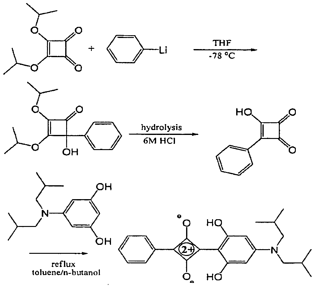
- Scheme 3 depicts a method of preparing asymmetric aryl squaraines.
- 3,4-disopropoxycyclobut-3-ene-1 ,2-dione is reacted with the aryllithium compound in THF at -78°C.
- the arylsquarate intermediate is extracted with DCM, and subsequently hydrolyzed with HCI to form the arylsquarate.
- the asymmetric diarylsquaraine product is obtained by reacting the arylsquarate intermediate with the desired hydroxyl-substituted arylamine.
- the squaraine compounds described herein may be used in the preparation of organic photosensitive optoelectronic devices.
- the organic photosensitive optoelectronic devices described herein have at least one donor-acceptor heterojunction comprising at least one compound of formula (I):
- Yi'and Y 2 are independently selected from an optionally substituted amino group and an optionally substituted aryl group.
- the squaraine is asymmetric, i.e, Yi and Y 2 are different.
- the organic optoelectronic devices of the embodiments of described herein may be used, for example, to generate a usable electrical current from incident electromagnetic radiation (e.g., PV devices) or may be used to detect incident electromagnetic radiation.
- the devices described herein may be prepared by forming a photoactive region comprising at least one donor-acceptor heterojunction having at least one compound of formula (I).
- the photoactive region is the portion of the photosensitive device that absorbs electromagnetic radiation to generate excitons that may dissociate in order to generate an electrical current.
- the device is a solar cell and the donor-acceptor heterojunction is formed at an interface of a donor material comprising at least one compound of formula (I) and an acceptor material.
- Embodiments of the devices described herein may comprise an anode, a cathode, and a photoactive region between the anode and the cathode.
- Organic photosensitive optoelectronic devices may also include at least one transparent electrode to allow incident radiation to be absorbed by the device.
- Figure 1 shows an organic photosensitive optoelectronic device 100.
- Device 100 may include a substrate 110, an anode 115, an anode smoothing layer 120, a donor layer 125, an acceptor layer 130, a blocking layer 135, and a cathode 140.
- Cathode 140 may be a compound cathode having a first conductive layer and a second conductive layer.
- Device 100 may be fabricated by depositing the layers described, in order. Charge separation may occur predominantly at the organic heterojunction between donor layer 125 and acceptor layer 130. The built-in potential at the heterojunction is determined by the HOMO-LUMO energy level difference between the two materials contacting to form the heterojunction.
- the HOMO-LUMO gap offset between the donor and acceptor materials produces an electric field at the donor/acceptor interface that facilitates charge separation for excitons created within an exciton diffusion length of the interface.
- the substrate may be any suitable substrate that provides desired structural properties.
- the substrate may be flexible or rigid, planar or non-planar.
- the substrate may be transparent, translucent or opaque.
- Plastic and glass are examples of rigid substrate materials that may be used herein.
- Plastic and metal foils are examples of flexible substrate materials that may be used according to the present disclosure.
- the material and thickness of the substrate may be chosen to obtain desired structural and optical properties.
- Electrode and “contact” refer to layers that provide a medium for delivering photo-generated current to an external circuit or providing a bias voltage to the device. That is, an electrode, or contact, provides the interface between the active regions of an organic photosensitive optoelectronic device and a wire, lead, trace or other means for transporting the charge carriers to or from the external circuit.
- the opposing electrode may be a reflective material so that light which has passed through the cell without being absorbed is reflected back through the cell.
- a layer of material or a sequence of several layers of different materials is said to be “transparent” when the layer or layers permit at least 50% of the ambient electromagnetic radiation in relevant wavelengths to be transmitted through the layer or layers. Similarly, layers which permit some, but less that 50% transmission of ambient electromagnetic radiation in relevant wavelengths are said to be “semi-transparent.”
- top means farthest away from the substrate
- bottom means closest to the substrate.
- the bottom electrode is the electrode closest to the substrate, and is generally the first electrode fabricated.
- the bottom electrode has two surfaces, a bottom surface closest to the substrate, and a top surface further away from the substrate.
- a first layer is described as "disposed over” a second layer
- the first layer is disposed further away from substrate.
- a cathode may be described as “disposed over” an anode, even though there are various organic layers in between.
- the electrodes are composed of metals or "metal substitutes".
- metal is used to embrace both materials composed of an elementally pure metal, e.g., Mg, Ag, Au, or Al, and also metal alloys which are materials composed of two or more elementally pure metals, e.g., Mg and Ag together, denoted Mg:Ag.
- metal substitute refers to a material that is not a metal within the normal definition, but which has the metal-like properties that are desired in certain appropriate applications.
- Commonly used metal substitutes for electrodes and charge transfer layers would include doped wide-bandgap semiconductors, for example, transparent conducting oxides.
- Transparent conductive polymers may also be used.
- Non-limiting transparent conducting oxides include indium tin oxide (ITO), tin oxide (TO), gallium indium tin oxide (GITO), zinc oxide (ZO), and zinc indium tin oxide (ZITO), glass and transparent conductive polymers.
- Exemplary transparent conductive polymers include, for example, polyanaline (PANI).
- ITO is a highly doped degenerate n+ semiconductor with an optical bandgap of approximately 3.2 eV, rendering it transparent to wavelengths greater than approximately 390 nm.
- Another suitable metal substitute is the transparent conductive polymer polyanaline (PANI) and its chemical relatives.
- Metal substitutes may be further selected from a wide range of non-metallic materials, wherein the term “non-metallic” is meant to embrace a wide range of materials provided that the material is free of metal in its chemically uncombined form. When a metal is present in its chemically uncombined form, either alone or in combination with one or more other metals as an alloy, the metal may alternatively be referred to as being present in its metallic form or as being a "free metal".
- the metal substitute electrodes of the present invention may sometimes be referred to as "metal-free” wherein the term “metal-free” is expressly meant to embrace a material free of metal in its chemically uncombined form.
- Free metals typically have a form of metallic bonding that results from a sea of valence electrons which are free to move in an electronic conduction band throughout the metal lattice. While metal substitutes may contain metal constituents they are "non-metallic" on several bases. They are not pure free- metals nor are they alloys of free-metals. When metals are present in their metallic form, the electronic conduction band tends to provide, among other metallic properties, a high electrical conductivity as well as a high reflectivity for optical radiation.
- Embodiments of the present disclosure may include, as one or more of the transparent electrodes of the photosensitive optoelectronic device, a highly transparent, non-metallic, low resistance cathode such as disclosed in U.S. Patent No. 6,420,031 , to Parthasarathy et al. ("Parthasarathy ⁇ 31 "), or a highly efficient, low resistance metallic/non-metallic compound cathode such as disclosed in U .S. Patent No. 5,703,436 to Forrest et al. (“Forrest '436”), both incorporated herein by reference in their entirety.
- Each type of cathode may be prepared in a fabrication process that includes sputter depositing an ITO layer onto either an organic material, such as copper phthalocyanine (CuPc), to form a highly transparent, non-metallic, low resistance cathode or onto a thin Mg:Ag layer to form a highly efficient, low resistance metallic/non-metallic compound cathode.
- an organic material such as copper phthalocyanine (CuPc)
- CuPc copper phthalocyanine
- Parthasarathy ⁇ 31 discloses that an ITO layer onto which an organic layer had been deposited, instead of an organic layer onto which the ITO layer had been deposited, does not function as an efficient cathode.
- the ITO would be deposited onto the substrate, unless the layers were being deposited in the reverse orientation.
- an organic compound that facilitates the formation of crystalline or amorphous films may be utilized as a hole transporting material between the anode (e.g. , ITO) and the squaraine.
- the organic film-facilitating compound does not contribute to photon absorption and has suitable energetics with squaraines such as SQ.
- the presence of a layer of an organic film-facilitating compound may ensure that the ⁇ is not be in contact with the ITO, thus preventing loss of C 6 o inherent photocurrent.
- an organic film-facilitating compound does not trap charge according to its well known good hole mobility.
- cathode is used in the following manner. In a non- stacked PV device or a single unit of a stacked PV device under ambient irradiation and connected with a resistive load and with no externally applied voltage, e.g. , a PV device, electrons move to the cathode from the photo-conducting material.
- anode is used herein such that in a PV device under illumination, holes move to the anode from the photo-conducting material, which is equivalent to electrons moving in the opposite manner. It will be noted that as the terms are used herein, anodes and cathodes may be electrodes or charge transfer layers.
- An organic photosensitive device will comprise at least one photoactive region in which light is absorbed to form an excited state, or "exciton", which may subsequently dissociate into an electron and a hole.
- the dissociation of the exciton will typically occur at the heterojunction formed by the juxtaposition of an acceptor layer and a donor layer.
- the "photoactive region” may include donor layer 125 and acceptor layer ⁇ 30.
- the donor layer may comprise at least one compound of formula (I):
- Yi and Y 2 are independently selected from a substituted amino group or a substituted aryl group, or (b) Yi and Y 2 are independently selected from an optionally substituted amino group or an optionally substituted aryl group, wherein the squaraine compound is not symmetric.
- the organic photosensitive optoelectronic devices described herein may comprise at least two different squaraines to provide more efficient light harvesting at wavelengths ranging from 500 to 850 nm, when compared to a donor-acceptor heterojunction comprising, at most, one squaraine.
- Such squaraine compounds may be used alone or in addition to other donor materials.
- All references to compounds of formula (I), including, for example, the devices and methods comprising compounds of formula (I) are intended to encompass any salts or derivatives of these compounds.
- a compound of formula (I) may be present in a ketone or alcohol form rather than the charge separated form depicted.
- the acceptor material may be comprised of, for example, perylenes, naphthalenes, fullerenes or nanotubules.
- exemplary acceptor materials include ⁇ , C 70 , C 8 4, 3,4,9, 10-perylenetracarboxylic dianhydride (PTCDA), 3,4,9, 10- perylenetracarboxylic diimide (PTCDI), 3,4,9, 10-perylenetetracarboxylic-bis- benzimidazole (PTCBI), 1 ,4,5,8-naphthalenetetracarboxylic dianhydride (NTCDA), copper pthalocyanine (CuPc), and copper-hexadecafluoro-phthalocyanine (Fi 6 -CuPc).
- PTCDA 10-perylenetracarboxylic dianhydride
- PTCDI 10- perylenetracarboxylic diimide
- NTCBI 10-perylenetetracarboxylic-bis- benzimidazole
- the stacked organic layers include one or more exciton blocking layers (EBLs) as described in U.S. Patent No. 6,097, 147, Peumans et al, Applied Physics Letters 2000, 76, 2650-52, and co-pending application serial number 09/449,801 , filed Nov. 26, 1999, both incorporated herein by reference.
- EBLs exciton blocking layers
- an EBL can also act as a diffusion barrier to substances introduced during deposition of the electrodes.
- an EBL can be made thick enough to fill pinholes or shorting defects which could otherwise render an organic PV device non-functional. An EBL can therefore help protect fragile organic layers from damage produced when electrodes are deposited onto the organic materials. EBLs can also function as optical spacers that allow for the focusing of optical field peaks in the active area of the cell.
- Exemplary electron or exciton blocking materials include, for example, bathocuproine (BCP), bathophenanthroline (BPhen), 3,4,9,10- perylenetetracarboxylicbis-benzimidazole (PTCBI), 1 ,3,5-tris(N-phenylbenzimidazol-2- yl)benzene (TPBi), tris(acetylacetonato) ruthenium(lll) (RuAcaca3), and
- the EBL is situated between the acceptor layer and the cathode.
- EBLs derive their exciton blocking property from having a LUMO-HOMO energy gap substantially larger than that of the adjacent organic semiconductor from which excitons are being blocked. Thus, the confined excitons are prohibited from existing in the EBL due to energy considerations. While it is desirable for the EBL to block excitons, it is not desirable for the EBL to block all charge. However, due to the nature of the adjacent energy levels, an EBL may block one sign of charge carrier. By design, an EBL will exist between two other layers, usually an organic photosensitive semiconductor layer and an electrode or charge transfer layer or charge recombination layers. The adjacent electrode or charge transfer layer will be in context either a cathode or an anode.
- the material for an EBL in a given position in a device will be chosen so that the desired sign of carrier will not be impeded in its transport to or from the electrode or charge transfer layer.
- Proper energy level alignment ensures that no barrier to charge transport exists, preventing an increase in series resistance.
- the EBL layer may be doped with a suitable dopant, including but not limited to 3,4,9, 10-perylenetracarboxylic dianhydride (PTCDA), 3,4,9, 10-perylenetracarboxylic diimide (PTCDI), 3,4,9, 10-perylenetetracarboxylic-bis- benzimidazole (PTCBI), 1 , 4, 5, 8-naphthalenetetracarboxylic dianhydride (NTCDA), and derivatives thereof.
- PTCDA 10-perylenetracarboxylic dianhydride
- PTCDI 10-perylenetracarboxylic diimide
- NTCBI 10-perylenetetracarboxylic-bis- benzimidazole
- NTCDA 10-perylenetetracarboxylic-bis- benzimidazole
- Representative embodiments may also comprise transparent charge transfer layers or charge recombination layers.
- charge transfer layers are distinguished from acceptor and donor layers by the fact that charge transfer layers are frequently, but not necessarily, inorganic (often metals) and they may be chosen not to be photoconductively active.
- charge transfer layer is used herein to refer to layers similar to but different from electrodes in that a charge transfer layer only delivers charge carriers from one subsection of an optoelectronic device to the adjacent subsection.
- charge recombination layer is used herein to refer to layers similar to but different from electrodes in that a charge recombination layer allows for the recombination of electrons and holes between adjacent charge carrier layers and may also enhance internal optical field strength near one or more active layers.
- a charge recombination layer can be constructed of semi-transparent metal
- an anode-smoothing layer may be situated between the anode and the donor layer.
- One material for this layer comprises a film of 3,4-polyethylenedioxythiophene:polystyrenesulfonate (PEDOT:PSS).
- PEDOT:PSS 3,4-polyethylenedioxythiophene:polystyrenesulfonate
- ITO anode
- CuPc donor layer
- the improved fabrication yields is a result of the ability of the spin-coated PEDOT:PSS film to planarize the ITO, whose rough surface could otherwise result in shorts through the thin molecular layers.
- one or more of the layers may be treated with plasma prior to depositing the next layer.
- the layers may be treated, for example, with a mild argon or oxygen plasma. This treatment may help to reduce the series resistance. It is particularly advantageous that the PEDOT:PSS layer be subject to a mild plasma treatment prior to deposition of the next layer.
- the layers may have various sublayers.
- the names given to the various layers herein are not intended to be strictly limiting.
- Organic layers that are not a part ' of the photoactive region, i.e., organic layers that generally do not absorb photons that make a significant contribution to photocurrent, may be referred to as "non-photoactive layers.”
- non-photoactive layers include EBLs and anode-smoothing layers. Other types of non-photoactive layers may also be used.
- Non-limiting examples of organic materials for use in the photoactive layers of a photosensitive device include cyclometallated organometallic compounds.
- organometallic as used herein is as generally understood by one of ordinary skill in the art and as given, for example, in “Inorganic Chemistry” (2nd
- organometallic refers to compounds which have an organic group bonded to a metal through a carbon-metal bond. This class does not include per se coordination compounds, which are substances having only donor bonds from heteroatoms, such as metal complexes of amines, halides, pseudohalides (CN, etc.), and the like.
- organometallic compounds generally comprise, in addition to one or more carbon-metal bonds to an organic species, one or more donor bonds from a
- the carbon-metal bond to an organic species refers to a direct bond between a metal and a carbon atom of an organic group, such as phenyl, alkyl, alkenyl, etc., but does not refer to a metal bond to an "inorganic carbon," such as the carbon of CN or CO.
- the term cyclometallated refers to compounds that comprise an bidentate organometallic ligand so that, upon bonding to a metal, a ring structure is formed that includes the metal as one of the ring members.
- Organic layers may be fabricated using vacuum deposition, spin coating, organic vapor-phase deposition, inkjet printing and other methods known in the art.
- the donor-acceptor heterojunction is disposed over a substrate.
- the organic photosensitive optoelectronic device described herein may be prepared, for example, by depositing the at least one compound of formula (I) by one or more processes chosen from vacuum deposition and solution processing.
- Solution processing may comprise one or more technique chosen from spin coating, spray coating, dip coating, or doctor's blading.
- the squaraine compounds may be sublimed during vacuum deposition one or more times.
- sublimation may include but is not limited to vacuum deposition. Accordingly, sublimation may be carried out at any temperature and pressure suitable for depositing the materials.
- Subliming the squaraine compounds may afford certain benefits regarding purification.
- Subliming squaraines one or more times may provide amorphous films and better properties than non-sublimed films. While not being bound by any theory, it is believed that multiple sublimation steps act as purification steps, for example, to remove trapping impurities otherwise present, whether the resulting film is amorphous or crystalline.
- the squaraine compound of formula (I) is deposited at a rate ranging from 0.1 to 1.5 A sec, such as 0.2 to 1.0 A/sec, or even 0.2 to 0.6 A/sec. In one embodiment, the deposited squaraine compound of formula (I) has a thickness of 100 A or less, such as 65 A or less, even 50 A or less. As used herein the "thickness" refers to the thickness of the layer (e.g., the thickness of the layer of the squaraine compound) as opposed to the molecular characteristics (e.g., bond distances) of materials that form any given layer.
- the squaraine materials described herein can be a good donor in any device architecture.
- the squaraine material being used in an architectural arrangement chosen from planar, bulk heterojunctions, hybrid-planar mixed, nanocrystalline bulk heterojunctions, and the like.
- this material may be a good donor toward C 6 o in any device architecture.
- the squaraines described herein may also be a good donor for other acceptors.
- the disclosed squaraines could even be an acceptor for a given donor, again in a range of device architectures, such as those previously mentioned.
- heterojunction according to the present disclosure may comprise at least two different squaraine compounds described herein, such as mixture of two different squaraines.
- squaraine compounds described herein such as mixture of two different squaraines.
- methods of making such a device comprising a mixture of two or more different squaraines.
- the deposited squaraine compound forms a discontinuous layer.
- the term "discontinuous layer” is intended to mean a layer (e.g., a layer of a squaraine compound) that does not have a uniform thickness throughout the layer.
- the discontinuous layer of the invention is a layer that does not completely cover all portions of the layer (or substrate) onto which it was deposited, thereby resulting in some portions of that layer being exposed after depositing the discontinuous layer.
- the deposited squaraine compound forms isolated nanoscale domains.
- isolated nanoscale domains is used to contrast uniform thin film, and thus refers to a portion of the deposited squaraine compound that exists as 1 -50 nm domains, forming a discontinuous thin film.
- C 60 is deposited such that it is in contact with the squaraine compound in the organic photosensitive optoelectronic device.
- the squaraine layer is ultrathin, such that the C 6 o has direct contact with the substrate.
- the organic photosensitive optoelectronic devices described herein may function as a device or solar cell, photodetector or photoconductor. Whenever the organic photosensitive optoelectronic devices function as a PV device, the materials used in the photoconductive organic layers and the thicknesses thereof may be selected, for example, to optimize the external quantum efficiency of the device. Whenever the organic photosensitive optoelectronic devices function as
- the materials used in the photoconductive organic layers and the thicknesses thereof may be selected, for example, to maximize the sensitivity of the device to desired spectral regions.
- the exciton diffusion length, I_D is desirable for the exciton diffusion length, I_D, to be greater than or comparable to the layer thickness, L, since it is believed that most exciton dissociation will occur at an interface. If L D is less than L, then many excitons may recombine before dissociation. ' It is further desirable for the total photoconductive layer thickness to be of the order of the electromagnetic radiation absorption length, 1/a, where a is the absorption coefficient, so that nearly all of the radiation incident on the PV device is absorbed to produce excitons.
- the photoconductive layer thickness should be as thin as possible to avoid excess series resistance due to the high bulk resistivity of organic
- the organic photosensitive optoelectronic devices described herein may function as photodetectors.
- the device may be a multilayer organic device, for example as described in U.S. Patent No. 6,972,431 , incorporated herein by reference in its entirety.
- an external electric field may be generally applied to facilitate extraction of the separated charges.
- a concentrator or trapping configuration may be employed to increase the efficiency of the organic photosensitive optoelectronic device, where photons are forced to make multiple passes through the thin absorbing regions.
- U.S. Patent Nos. 6,333,458 and 6,440,769 incorporated herein by reference in their entirety, addresses this issue by using structural designs that enhance the photoconversion efficiency of photosensitive optoelectronic devices by optimizing the optical geometry for high absorption and for use with optical concentrators that increase collection efficiency.
- Such geometries for photosensitive devices substantially increase the optical path through the material by trapping the incident radiation within a reflective cavity or waveguiding structure, and thereby recycling light by multiple reflections through the photoresponsive material.
- the geometries disclosed in U.S. Patent Nos. 6,333,458 and 6,440,769 therefore enhance the external quantum efficiency of the devices without causing substantial increase in bulk resistance.
- a first reflective layer included in the geometry of such devices is a first reflective layer; a transparent insulating layer which should be longer than the optical coherence length of the incident light in all dimensions to prevent optical microcavity interference effects; a transparent first electrode layer adjacent the transparent insulating layer; a photosensitive heterostructure adjacent the transparent electrode; and a second electrode which is also reflective.
- one or more coatings may be used to focus optical energy into desired regions of a device. See, e.g., U.S. Patent No. 7,196,835, the disclosures of which, specifically related to such coatings, are herein incorporated by reference.
- Various devices made according to the foregoing disclosures were made and tested. Results of these tests are provided in Tables 1 and 2, below.
- Table 2b Photophysics data of aryl squaraines in select solvents.
- Photovoltaic cells were grown on ITO-coated glass substrates that were solvent cleaned and treated in UV-ozone for 10 minutes immediately prior to loading into a high vacuum ( ⁇ 3 x 10 "6 Torr) chamber.
- the organic materials CuPc (Aldrich), C 6 o (MTR Limited), and 2,9-dimethyl-4,7-diphenyl-1 , 10-phenanthroline (BCP) (Aldrich) were purified by sublimation prior to use.
- Metal cathode materials such as Al (Alfa Aesar) were used as received.
- the squaraine solutions were prepared with different anhydrous solvents. The thickness of the squariane layeres was controlled via the concentration of squaraine solution. In this method, the donor layer was spin casted from squaraine solution on precleaned ITO substrates. The film was then transferred to the deposition chamber.
- the other functional layers were sequentially grown by vacuum thermal evaporation at the following rates: C 60 (4 A sec), and 2,9-dimethyl-4,7-diphenyl-1 , 10- phenanthroline (BCP) (2A/sec) and metal: 1000 A thick Al (2.5 A /sec).
- BCP 2,9-dimethyl-4,7-diphenyl-1 , 10- phenanthroline
- metal 1000 A thick Al (2.5 A /sec).
- the cathode was evaporated through a shadow mask with 1 mm diameter openings.
- Current- voltage (J-V) characteristics of PV cells were measured under simulated AM1.5G solar illumination (Oriel Instruments) using a Keithley 2420 3A Source Meter. The external quantum efficiency was also measured.
- DPSQ formed shiny green crystals in the solid state. Compared with parent SQ, its solution absorption was red shifted to about 674 nm in dichloromethane (DCM) solvent. Comparatively, the spin casted DPSQ film covered a range of about from 550 nm to 800 nm.
- the solution processed DPSQ device was configured as ITO/DPSQ ( x mg/ml)/C60 (400 A)/ BCP (100 A)/AI. With about 0.1 Ev deeper of a HOMO than the parent SQ, the DPSQ device generated about 200 mV higher Voc than SQ solution-processed devices.
- the DPSQ film made with chloroform was the smoothest with RMS of about 1.1 nm, while the film with chlorobenzene and toluene exhibited an RMS of about 1 1 nm.
- the DPSQ device cast from chloroform generated the following results:
- 1-NPSQ and 2-NPSQ exhibit extended ⁇ conjugations, which may help to further enhance the charge transport ability of squaraine donors.
- the 1-NPSQ and 2-NPSQ are isomers with the same
- a 1-NPSQ device was constructed as ITO/M0O3 (80 A)/1-NPSQ (x mg/ml)/C 60 (400 A)/ BCP (100 A)/AI.
- the 1-NPSQ film was spin casted from the 1 ,2-dichlorobenzene solution and annealed at different temperatures for 10 minutes.
- Blends of SQ and USSQ are shown in Figure 6. Blends of DPUSQ or USSQ with symmetrical squaraines were also tested. The blending idea may be applied in both the vapor deposited and solution process techniques. With 1 :1 weight ratio of DPUSQ and 1-NPSQ, device efficiencies were observed at about 2.38% without losing the FF of about 0.52. The Voc and J S c are about 0.81 V and about 5.43 mA/cm 2 . The change of V 0 c is expected because of different morphology is generated by mixing two donors. However, the new USSQ and DPUSQ are conductive enough to be mixed with aryl squaraines.
Abstract
Description


Claims


Priority Applications (6)
| Application Number | Priority Date | Filing Date | Title |
|---|---|---|---|
| CA2826909A CA2826909A1 (en) | 2011-02-09 | 2012-02-07 | Organic photosensitive devices comprising aryl squaraines and methods of making the same |
| JP2013553491A JP2014510804A (en) | 2011-02-09 | 2012-02-07 | Organic photosensitive device comprising aryl squaraine and method for producing the same |
| KR1020137023465A KR20140115238A (en) | 2011-02-09 | 2012-02-07 | Organic photosensitive devices comprising aryl squaraines and methods of making the same |
| AU2012216234A AU2012216234A1 (en) | 2011-02-09 | 2012-02-07 | Organic photosensitive devices comprising aryl squaraines and methods of making the same |
| CN201280008386.XA CN103797075A (en) | 2011-02-09 | 2012-02-07 | Organic photosensitive devices comprising aryl squaraines and methods of making the same |
| EP12708183.4A EP2673321A2 (en) | 2011-02-09 | 2012-02-07 | Organic photosensitive devices comprising aryl squaraines and methods of making the same |
Applications Claiming Priority (4)
| Application Number | Priority Date | Filing Date | Title |
|---|---|---|---|
| US201161441153P | 2011-02-09 | 2011-02-09 | |
| US61/441,153 | 2011-02-09 | ||
| US201161479231P | 2011-04-26 | 2011-04-26 | |
| US61/479,231 | 2011-04-26 |
Publications (2)
| Publication Number | Publication Date |
|---|---|
| WO2012109232A2 true WO2012109232A2 (en) | 2012-08-16 |
| WO2012109232A3 WO2012109232A3 (en) | 2012-10-26 |
Family
ID=45814651
Family Applications (1)
| Application Number | Title | Priority Date | Filing Date |
|---|---|---|---|
| PCT/US2012/024131 WO2012109232A2 (en) | 2011-02-09 | 2012-02-07 | Organic photosensitive devices comprising aryl squaraines and methods of making the same |
Country Status (9)
| Country | Link |
|---|---|
| US (3) | US20120248419A1 (en) |
| EP (1) | EP2673321A2 (en) |
| JP (1) | JP2014510804A (en) |
| KR (1) | KR20140115238A (en) |
| CN (2) | CN105037246A (en) |
| AU (1) | AU2012216234A1 (en) |
| CA (1) | CA2826909A1 (en) |
| TW (1) | TW201240948A (en) |
| WO (1) | WO2012109232A2 (en) |
Cited By (6)
| Publication number | Priority date | Publication date | Assignee | Title |
|---|---|---|---|---|
| JP2014169284A (en) * | 2013-02-07 | 2014-09-18 | Yamagata Univ | Asymmetric squarilium derivative, donor material comprising the same, organic thin film solar cell using the same |
| JP2016500919A (en) * | 2012-10-11 | 2016-01-14 | ザ リージェンツ オブ ザ ユニヴァシティ オブ ミシガン | Polymer photovoltaic technology using a squaraine donor additive. |
| JP2018510845A (en) * | 2015-01-27 | 2018-04-19 | ソニー株式会社 | Squaline and thiophene-based molecules as materials for organic photoelectric conversion layers in organic photodiodes |
| JP2018121068A (en) * | 2012-10-05 | 2018-08-02 | ユニバーシティ オブ サザン カリフォルニア | Energy sensitization of acceptors and donors in organic photovoltaics |
| US20200091355A1 (en) * | 2018-09-14 | 2020-03-19 | Ubiquitous Energy, Inc. | Method and system for multilayer transparent electrode for transparent photovoltaic devices |
| US11261374B2 (en) * | 2018-09-14 | 2022-03-01 | Konica Minolta, Inc. | Squarylium compound, light-emitting composition, and light-emitting film |
Families Citing this family (21)
| Publication number | Priority date | Publication date | Assignee | Title |
|---|---|---|---|---|
| US20100065112A1 (en) * | 2008-09-15 | 2010-03-18 | Thompson Mark E | Organic Photosensitive Devices Comprising a Squaraine Containing Organoheterojunction and Methods of Making Same |
| CN105037246A (en) * | 2011-02-09 | 2015-11-11 | 密歇根大学董事会 | Organic photosensitive devices comprising aryl squaraines and methods of making the same |
| KR20150088830A (en) | 2012-11-22 | 2015-08-03 | 더 리젠츠 오브 더 유니버시티 오브 미시간 | Use of inverse quasi-epitaxy to modify order during post-deposition processing or organic photovoltaics |
| CN103214410B (en) * | 2013-04-03 | 2016-01-06 | 四川大学 | A series of asymmetric side's acid cyanines small molecules and its preparation method and application |
| US9991453B2 (en) * | 2013-05-22 | 2018-06-05 | Konica Minolta, Inc. | Electronic device, organic electroluminescent element, organic thin-film solar cell, and dye-sensitized solar cell |
| JP5403179B1 (en) * | 2013-05-22 | 2014-01-29 | コニカミノルタ株式会社 | Charge transfer thin film |
| JP6606631B6 (en) * | 2015-01-13 | 2020-01-15 | 康文 榎波 | Light modulator |
| KR102258497B1 (en) * | 2015-02-04 | 2021-05-28 | 삼성전자주식회사 | Organic photoelectric device, image sensor and electronic device |
| JP6581374B2 (en) * | 2015-03-24 | 2019-09-25 | 株式会社日本触媒 | Method for storing or using a composition comprising an oxocarbon-based compound |
| JP6736077B2 (en) * | 2015-06-03 | 2020-08-05 | 国立大学法人山形大学 | Novel squarylium derivative and organic thin-film solar cell using the same |
| CN106083695B (en) * | 2016-06-21 | 2018-07-24 | 四川大学 | A series of sour cyanines small molecule in asymmetry sides containing Azulene and preparation method and application |
| TWI741010B (en) * | 2016-08-29 | 2021-10-01 | 日商富士軟片股份有限公司 | Composition, film, near-infrared cut filter, pattern forming method, laminate, solid-state imaging element, image display device, camera module, and infrared sensor |
| KR102087260B1 (en) | 2016-09-26 | 2020-03-10 | 삼성에스디아이 주식회사 | Novel compound, core-shell dye, photosensitive resin composition including the same, and color filter |
| KR102087259B1 (en) | 2016-09-28 | 2020-03-10 | 삼성에스디아이 주식회사 | Novel compound, core-shell dye, photosensitive resin composition including the same, and color filter |
| JP7044108B2 (en) * | 2017-05-08 | 2022-03-30 | コニカミノルタ株式会社 | Organic electroluminescence elements, display devices, lighting devices |
| JP6945841B2 (en) * | 2017-06-19 | 2021-10-06 | 国立大学法人山形大学 | Near-infrared absorption squarylium derivatives and organic electronic devices containing them |
| KR102491496B1 (en) | 2018-01-05 | 2023-01-20 | 삼성전자주식회사 | Photoelectronic device and image sensor and electronic device |
| JP6964752B2 (en) * | 2018-02-28 | 2021-11-10 | 富士フイルム株式会社 | Curable composition, cured product, color filter, manufacturing method of color filter, solid-state image sensor and image display device |
| WO2020013089A1 (en) * | 2018-07-13 | 2020-01-16 | 富士フイルム株式会社 | Coloring composition, film, color filter, method for manufacturing color filter, solid-state imaging element, and image display device |
| CN109053531B (en) * | 2018-08-14 | 2020-11-27 | 清华大学 | Asymmetric squarylium cyanine material and preparation method and application thereof |
| KR102627682B1 (en) * | 2019-08-13 | 2024-01-24 | 후지필름 가부시키가이샤 | Compositions, membranes, optical filters and methods for producing the same, solid-state imaging devices, infrared sensors, camera modules, and compounds |
Citations (10)
| Publication number | Priority date | Publication date | Assignee | Title |
|---|---|---|---|---|
| US5703436A (en) | 1994-12-13 | 1997-12-30 | The Trustees Of Princeton University | Transparent contacts for organic devices |
| US6097147A (en) | 1998-09-14 | 2000-08-01 | The Trustees Of Princeton University | Structure for high efficiency electroluminescent device |
| US6333458B1 (en) | 1999-11-26 | 2001-12-25 | The Trustees Of Princeton University | Highly efficient multiple reflection photosensitive optoelectronic device with optical concentrator |
| US6352777B1 (en) | 1998-08-19 | 2002-03-05 | The Trustees Of Princeton University | Organic photosensitive optoelectronic devices with transparent electrodes |
| US6420031B1 (en) | 1997-11-03 | 2002-07-16 | The Trustees Of Princeton University | Highly transparent non-metallic cathodes |
| US6440769B2 (en) | 1999-11-26 | 2002-08-27 | The Trustees Of Princeton University | Photovoltaic device with optical concentrator and method of making the same |
| US6580027B2 (en) | 2001-06-11 | 2003-06-17 | Trustees Of Princeton University | Solar cells using fullerenes |
| US6657378B2 (en) | 2001-09-06 | 2003-12-02 | The Trustees Of Princeton University | Organic photovoltaic devices |
| US6972431B2 (en) | 2003-11-26 | 2005-12-06 | Trustees Of Princeton University | Multilayer organic photodetectors with improved performance |
| US7196835B2 (en) | 2004-06-01 | 2007-03-27 | The Trustees Of Princeton University | Aperiodic dielectric multilayer stack |
Family Cites Families (31)
| Publication number | Priority date | Publication date | Assignee | Title |
|---|---|---|---|---|
| US3824099A (en) * | 1973-01-15 | 1974-07-16 | Ibm | Sensitive electrophotographic plates |
| JPS60169453A (en) * | 1984-02-13 | 1985-09-02 | Mitsubishi Chem Ind Ltd | 2,4-bis(2'-monosubstituted amino-4'-disubstituted aminophenyl)cyclobutenediylium-1,3-diolate |
| EP0172321B1 (en) * | 1984-07-27 | 1987-11-19 | International Business Machines Corporation | Squarylium charge generating dye and electrophotographic photoconductor |
| JPH0727245B2 (en) * | 1986-11-25 | 1995-03-29 | 富士ゼロックス株式会社 | Electrophotographic photoreceptor |
| JP2567238B2 (en) * | 1987-03-25 | 1996-12-25 | 日本化薬株式会社 | Resin plate for light collection |
| JP2546302B2 (en) * | 1987-12-04 | 1996-10-23 | 富士ゼロックス株式会社 | Method for producing squarylium compound |
| JPH07107029B2 (en) * | 1987-12-04 | 1995-11-15 | 富士ゼロックス株式会社 | Novel squarylium compound and method for producing the same |
| JPH07107030B2 (en) * | 1987-12-04 | 1995-11-15 | 富士ゼロックス株式会社 | Novel squarylium compound and method for producing the same |
| US4886722A (en) * | 1988-04-29 | 1989-12-12 | Xerox Corporation | Photoconductive imaging members with unsymmetrical squaraine compositions |
| JPH0725153A (en) * | 1993-07-14 | 1995-01-27 | Fuji Photo Film Co Ltd | Thermal recording material for infrared laser |
| ATE267230T1 (en) * | 1999-12-16 | 2004-06-15 | Kyowa Hakko Kogyo Kk | SQUARYLIUM COMPOUNDS AND THEIR USE IN THE PRODUCTION OF RECORDING MEDIA |
| JP4183919B2 (en) * | 2000-03-07 | 2008-11-19 | 株式会社リコー | Optical recording medium and optical recording method using the same |
| EP1316586A4 (en) * | 2000-09-04 | 2004-10-27 | Mitsubishi Chem Corp | Diphenylsquarylium compound and display filter containing the same |
| US7554842B2 (en) * | 2001-09-17 | 2009-06-30 | Sandisk Corporation | Multi-purpose non-volatile memory card |
| JP4945873B2 (en) * | 2001-09-27 | 2012-06-06 | コニカミノルタホールディングス株式会社 | Semiconductor for photoelectric conversion material, photoelectric conversion element and solar cell |
| US7687633B2 (en) * | 2003-12-18 | 2010-03-30 | Kyowa Hakko Chemical Co., Ltd. | Filters for electronic display devices |
| WO2006041156A1 (en) * | 2004-10-14 | 2006-04-20 | Kyowa Hakko Chemical Co., Ltd. | Squarylium compound, photo-electric converting material comprising the same, photo-electric converting element, and photoelectrochemical cell |
| TW200720842A (en) * | 2005-10-24 | 2007-06-01 | Kyowa Hakko Chemical Co Ltd | A squarilium compound and the short-wave length source photo polymerization composition using thereof |
| EP1970959A3 (en) * | 2007-03-12 | 2013-07-31 | FUJIFILM Corporation | Photoelectric conversion element and solid-state imaging device |
| JP5331309B2 (en) * | 2007-03-28 | 2013-10-30 | 富士フイルム株式会社 | Photoelectric conversion device and solid-state imaging device |
| JP2009015113A (en) * | 2007-07-06 | 2009-01-22 | Konica Minolta Business Technologies Inc | Toner for electrophotography and polymer dye |
| JP2009139911A (en) * | 2007-11-12 | 2009-06-25 | Kyowa Hakko Chemical Co Ltd | Optical filter containing squarylium compound |
| JP5125549B2 (en) * | 2008-01-30 | 2013-01-23 | コニカミノルタビジネステクノロジーズ株式会社 | Color toner for electrophotography |
| JP2009280537A (en) * | 2008-05-23 | 2009-12-03 | Kyowa Hakko Chemical Co Ltd | Photopolymerizable composition containing squarylium compound and optical recording medium for volume-type hologram |
| US20100065112A1 (en) * | 2008-09-15 | 2010-03-18 | Thompson Mark E | Organic Photosensitive Devices Comprising a Squaraine Containing Organoheterojunction and Methods of Making Same |
| CA2737477A1 (en) * | 2008-09-26 | 2010-04-01 | The Regents Of The University Of Michigan | Organic tandem solar cells |
| CN105037246A (en) * | 2011-02-09 | 2015-11-11 | 密歇根大学董事会 | Organic photosensitive devices comprising aryl squaraines and methods of making the same |
| AU2013292306A1 (en) * | 2012-07-19 | 2015-02-05 | The Regents Of The University Of Michigan | Multijunction organic photovoltaics incorporating solution and vacuum deposited active layers |
| CA2880519A1 (en) * | 2012-08-01 | 2014-02-06 | The Regents Of The University Of Michigan | Organic optoelectronics with electrode buffer layers |
| EP3101706A1 (en) * | 2012-10-11 | 2016-12-07 | The Regents of The University of Michigan | Polymer photovoltaics employing a squaraine donor additive |
| KR20170108068A (en) * | 2015-01-27 | 2017-09-26 | 소니 주식회사 | A squaraine molecule as a material for an organic photoelectric conversion layer in an organic photodiode |
-
2012
- 2012-02-07 CN CN201510321457.7A patent/CN105037246A/en active Pending
- 2012-02-07 US US13/368,040 patent/US20120248419A1/en not_active Abandoned
- 2012-02-07 AU AU2012216234A patent/AU2012216234A1/en not_active Abandoned
- 2012-02-07 JP JP2013553491A patent/JP2014510804A/en active Pending
- 2012-02-07 KR KR1020137023465A patent/KR20140115238A/en not_active Application Discontinuation
- 2012-02-07 CN CN201280008386.XA patent/CN103797075A/en active Pending
- 2012-02-07 EP EP12708183.4A patent/EP2673321A2/en not_active Withdrawn
- 2012-02-07 CA CA2826909A patent/CA2826909A1/en not_active Abandoned
- 2012-02-07 WO PCT/US2012/024131 patent/WO2012109232A2/en active Application Filing
- 2012-02-08 TW TW101104137A patent/TW201240948A/en unknown
-
2015
- 2015-09-14 US US14/853,256 patent/US10333079B2/en active Active
-
2019
- 2019-06-24 US US16/449,881 patent/US11944007B2/en active Active
Patent Citations (10)
| Publication number | Priority date | Publication date | Assignee | Title |
|---|---|---|---|---|
| US5703436A (en) | 1994-12-13 | 1997-12-30 | The Trustees Of Princeton University | Transparent contacts for organic devices |
| US6420031B1 (en) | 1997-11-03 | 2002-07-16 | The Trustees Of Princeton University | Highly transparent non-metallic cathodes |
| US6352777B1 (en) | 1998-08-19 | 2002-03-05 | The Trustees Of Princeton University | Organic photosensitive optoelectronic devices with transparent electrodes |
| US6097147A (en) | 1998-09-14 | 2000-08-01 | The Trustees Of Princeton University | Structure for high efficiency electroluminescent device |
| US6333458B1 (en) | 1999-11-26 | 2001-12-25 | The Trustees Of Princeton University | Highly efficient multiple reflection photosensitive optoelectronic device with optical concentrator |
| US6440769B2 (en) | 1999-11-26 | 2002-08-27 | The Trustees Of Princeton University | Photovoltaic device with optical concentrator and method of making the same |
| US6580027B2 (en) | 2001-06-11 | 2003-06-17 | Trustees Of Princeton University | Solar cells using fullerenes |
| US6657378B2 (en) | 2001-09-06 | 2003-12-02 | The Trustees Of Princeton University | Organic photovoltaic devices |
| US6972431B2 (en) | 2003-11-26 | 2005-12-06 | Trustees Of Princeton University | Multilayer organic photodetectors with improved performance |
| US7196835B2 (en) | 2004-06-01 | 2007-03-27 | The Trustees Of Princeton University | Aperiodic dielectric multilayer stack |
Non-Patent Citations (5)
| Title |
|---|
| GARY L. MIESSLER; DONALD A. TARR: "Inorganic Chemistry", 1998, PRENTICE HALL |
| PEUMANS ET AL., APPLIED PHYSICS LETTERS, vol. 76, 2000, pages 2650 - 2652 |
| See also references of EP2673321A2 |
| SON ET AL., POLY. SCI. PART A: POLYM. CHEM., vol. 48, 2009, pages 635 |
| TANG, APPL. PHYS LETT., vol. 48, 1986, pages 183 |
Cited By (8)
| Publication number | Priority date | Publication date | Assignee | Title |
|---|---|---|---|---|
| JP2018121068A (en) * | 2012-10-05 | 2018-08-02 | ユニバーシティ オブ サザン カリフォルニア | Energy sensitization of acceptors and donors in organic photovoltaics |
| JP2016500919A (en) * | 2012-10-11 | 2016-01-14 | ザ リージェンツ オブ ザ ユニヴァシティ オブ ミシガン | Polymer photovoltaic technology using a squaraine donor additive. |
| JP2014169284A (en) * | 2013-02-07 | 2014-09-18 | Yamagata Univ | Asymmetric squarilium derivative, donor material comprising the same, organic thin film solar cell using the same |
| JP2018510845A (en) * | 2015-01-27 | 2018-04-19 | ソニー株式会社 | Squaline and thiophene-based molecules as materials for organic photoelectric conversion layers in organic photodiodes |
| US20180273760A1 (en) * | 2015-01-27 | 2018-09-27 | Sony Corporation | Squaraine-based molecules as material for organic photoelectric conversion layers in organic photodiodes |
| US11352500B2 (en) | 2015-01-27 | 2022-06-07 | Sony Corporation | Squaraine-based molecules as material for organic photoelectric conversion layers in organic photodiodes |
| US20200091355A1 (en) * | 2018-09-14 | 2020-03-19 | Ubiquitous Energy, Inc. | Method and system for multilayer transparent electrode for transparent photovoltaic devices |
| US11261374B2 (en) * | 2018-09-14 | 2022-03-01 | Konica Minolta, Inc. | Squarylium compound, light-emitting composition, and light-emitting film |
Also Published As
| Publication number | Publication date |
|---|---|
| CA2826909A1 (en) | 2012-08-16 |
| US10333079B2 (en) | 2019-06-25 |
| TW201240948A (en) | 2012-10-16 |
| WO2012109232A3 (en) | 2012-10-26 |
| AU2012216234A1 (en) | 2013-08-22 |
| US20160005983A1 (en) | 2016-01-07 |
| CN103797075A (en) | 2014-05-14 |
| US11944007B2 (en) | 2024-03-26 |
| EP2673321A2 (en) | 2013-12-18 |
| JP2014510804A (en) | 2014-05-01 |
| KR20140115238A (en) | 2014-09-30 |
| CN105037246A (en) | 2015-11-11 |
| US20120248419A1 (en) | 2012-10-04 |
| US20200303660A1 (en) | 2020-09-24 |
Similar Documents
| Publication | Publication Date | Title |
|---|---|---|
| US11944007B2 (en) | Organic photosensitive devices comprising aryl squaraines and methods of making the same | |
| US20200203638A1 (en) | Energy sensitization of acceptors and donors in organic photovoltaics | |
| AU2006259747B2 (en) | Organic double-heterostructure photovoltaic cells having reciprocal-carrier exciton blocking layer | |
| EP3036782B1 (en) | New absorber for organic heterojunction solar cells | |
| CA2588113C (en) | Organic photosensitive optoelectronic device having a phenanthroline exciton blocking layer | |
| US10374164B2 (en) | Organic photosensitive devices comprising a squaraine containing organoheterojunction and methods of making same | |
| US20050211974A1 (en) | Organic photosensitive devices | |
| US20090044864A1 (en) | Organic photosensitive optoelectronic devices with triplet harvesting | |
| JP2010270084A (en) | Indole derivative, and solar cell of organic thin film by using the same | |
| WO2011127475A1 (en) | Organic photovoltaic devices comprising solution- processed substituted metal-phthalocyanines and exhibiting near-ir photo-sensitivity |
Legal Events
| Date | Code | Title | Description |
|---|---|---|---|
| 121 | Ep: the epo has been informed by wipo that ep was designated in this application |
Ref document number: 12708183 Country of ref document: EP Kind code of ref document: A2 |
|
| REEP | Request for entry into the european phase |
Ref document number: 2012708183 Country of ref document: EP |
|
| WWE | Wipo information: entry into national phase |
Ref document number: 2012708183 Country of ref document: EP |
|
| ENP | Entry into the national phase |
Ref document number: 2826909 Country of ref document: CA Ref document number: 2013553491 Country of ref document: JP Kind code of ref document: A |
|
| NENP | Non-entry into the national phase |
Ref country code: DE |
|
| ENP | Entry into the national phase |
Ref document number: 2012216234 Country of ref document: AU Date of ref document: 20120207 Kind code of ref document: A |
|
| ENP | Entry into the national phase |
Ref document number: 20137023465 Country of ref document: KR Kind code of ref document: A |