WO2011032624A1 - Organic electroluminescent device - Google Patents
Organic electroluminescent device Download PDFInfo
- Publication number
- WO2011032624A1 WO2011032624A1 PCT/EP2010/005022 EP2010005022W WO2011032624A1 WO 2011032624 A1 WO2011032624 A1 WO 2011032624A1 EP 2010005022 W EP2010005022 W EP 2010005022W WO 2011032624 A1 WO2011032624 A1 WO 2011032624A1
- Authority
- WO
- WIPO (PCT)
- Prior art keywords
- layer
- electroluminescent device
- organic electroluminescent
- derivatives
- electron transport
- Prior art date
Links
Classifications
-
- H—ELECTRICITY
- H10—SEMICONDUCTOR DEVICES; ELECTRIC SOLID-STATE DEVICES NOT OTHERWISE PROVIDED FOR
- H10K—ORGANIC ELECTRIC SOLID-STATE DEVICES
- H10K50/00—Organic light-emitting devices
-
- H—ELECTRICITY
- H10—SEMICONDUCTOR DEVICES; ELECTRIC SOLID-STATE DEVICES NOT OTHERWISE PROVIDED FOR
- H10K—ORGANIC ELECTRIC SOLID-STATE DEVICES
- H10K50/00—Organic light-emitting devices
- H10K50/10—OLEDs or polymer light-emitting diodes [PLED]
- H10K50/14—Carrier transporting layers
-
- H—ELECTRICITY
- H10—SEMICONDUCTOR DEVICES; ELECTRIC SOLID-STATE DEVICES NOT OTHERWISE PROVIDED FOR
- H10K—ORGANIC ELECTRIC SOLID-STATE DEVICES
- H10K50/00—Organic light-emitting devices
- H10K50/10—OLEDs or polymer light-emitting diodes [PLED]
- H10K50/14—Carrier transporting layers
- H10K50/16—Electron transporting layers
-
- C—CHEMISTRY; METALLURGY
- C09—DYES; PAINTS; POLISHES; NATURAL RESINS; ADHESIVES; COMPOSITIONS NOT OTHERWISE PROVIDED FOR; APPLICATIONS OF MATERIALS NOT OTHERWISE PROVIDED FOR
- C09B—ORGANIC DYES OR CLOSELY-RELATED COMPOUNDS FOR PRODUCING DYES, e.g. PIGMENTS; MORDANTS; LAKES
- C09B57/00—Other synthetic dyes of known constitution
- C09B57/008—Triarylamine dyes containing no other chromophores
-
- C—CHEMISTRY; METALLURGY
- C09—DYES; PAINTS; POLISHES; NATURAL RESINS; ADHESIVES; COMPOSITIONS NOT OTHERWISE PROVIDED FOR; APPLICATIONS OF MATERIALS NOT OTHERWISE PROVIDED FOR
- C09B—ORGANIC DYES OR CLOSELY-RELATED COMPOUNDS FOR PRODUCING DYES, e.g. PIGMENTS; MORDANTS; LAKES
- C09B57/00—Other synthetic dyes of known constitution
- C09B57/10—Metal complexes of organic compounds not being dyes in uncomplexed form
-
- H—ELECTRICITY
- H10—SEMICONDUCTOR DEVICES; ELECTRIC SOLID-STATE DEVICES NOT OTHERWISE PROVIDED FOR
- H10K—ORGANIC ELECTRIC SOLID-STATE DEVICES
- H10K50/00—Organic light-emitting devices
- H10K50/10—OLEDs or polymer light-emitting diodes [PLED]
- H10K50/11—OLEDs or polymer light-emitting diodes [PLED] characterised by the electroluminescent [EL] layers
-
- H—ELECTRICITY
- H10—SEMICONDUCTOR DEVICES; ELECTRIC SOLID-STATE DEVICES NOT OTHERWISE PROVIDED FOR
- H10K—ORGANIC ELECTRIC SOLID-STATE DEVICES
- H10K71/00—Manufacture or treatment specially adapted for the organic devices covered by this subclass
-
- H—ELECTRICITY
- H10—SEMICONDUCTOR DEVICES; ELECTRIC SOLID-STATE DEVICES NOT OTHERWISE PROVIDED FOR
- H10K—ORGANIC ELECTRIC SOLID-STATE DEVICES
- H10K85/00—Organic materials used in the body or electrodes of devices covered by this subclass
-
- H—ELECTRICITY
- H10—SEMICONDUCTOR DEVICES; ELECTRIC SOLID-STATE DEVICES NOT OTHERWISE PROVIDED FOR
- H10K—ORGANIC ELECTRIC SOLID-STATE DEVICES
- H10K85/00—Organic materials used in the body or electrodes of devices covered by this subclass
- H10K85/60—Organic compounds having low molecular weight
- H10K85/649—Aromatic compounds comprising a hetero atom
- H10K85/654—Aromatic compounds comprising a hetero atom comprising only nitrogen as heteroatom
-
- H—ELECTRICITY
- H10—SEMICONDUCTOR DEVICES; ELECTRIC SOLID-STATE DEVICES NOT OTHERWISE PROVIDED FOR
- H10K—ORGANIC ELECTRIC SOLID-STATE DEVICES
- H10K85/00—Organic materials used in the body or electrodes of devices covered by this subclass
- H10K85/60—Organic compounds having low molecular weight
- H10K85/649—Aromatic compounds comprising a hetero atom
- H10K85/655—Aromatic compounds comprising a hetero atom comprising only sulfur as heteroatom
-
- H—ELECTRICITY
- H10—SEMICONDUCTOR DEVICES; ELECTRIC SOLID-STATE DEVICES NOT OTHERWISE PROVIDED FOR
- H10K—ORGANIC ELECTRIC SOLID-STATE DEVICES
- H10K85/00—Organic materials used in the body or electrodes of devices covered by this subclass
- H10K85/60—Organic compounds having low molecular weight
- H10K85/649—Aromatic compounds comprising a hetero atom
- H10K85/656—Aromatic compounds comprising a hetero atom comprising two or more different heteroatoms per ring
-
- H—ELECTRICITY
- H10—SEMICONDUCTOR DEVICES; ELECTRIC SOLID-STATE DEVICES NOT OTHERWISE PROVIDED FOR
- H10K—ORGANIC ELECTRIC SOLID-STATE DEVICES
- H10K2102/00—Constructional details relating to the organic devices covered by this subclass
- H10K2102/301—Details of OLEDs
- H10K2102/351—Thickness
-
- H—ELECTRICITY
- H10—SEMICONDUCTOR DEVICES; ELECTRIC SOLID-STATE DEVICES NOT OTHERWISE PROVIDED FOR
- H10K—ORGANIC ELECTRIC SOLID-STATE DEVICES
- H10K50/00—Organic light-emitting devices
- H10K50/10—OLEDs or polymer light-emitting diodes [PLED]
- H10K50/14—Carrier transporting layers
- H10K50/16—Electron transporting layers
- H10K50/167—Electron transporting layers between the light-emitting layer and the anode
Definitions
- the present invention relates to organic electroluminescent devices which contain thick electron transport layers.
- OLEDs organic electroluminescent devices
- the structure of organic electroluminescent devices (OLEDs), in which organic semiconductors are used as functional materials, is described for example in US 4539507, US 5151629, EP 0676461 and US Pat
- WO 98/27136 A development in the field of organic electroluminescent devices are phosphorescent OLEDs. These have significant advantages compared to fluorescent OLEDs due to the higher achievable efficiency.
- top emission in which a semitransparent cathode and a reflective anode form a microcavity. This will narrow the emission spectrum and improve color purity.
- top-emission OLEDs require process technology that is difficult to handle, such as For example, the thicknesses of the different layers must be set very accurately.
- top-emission OLEDs are technically more complex to implement due to the more complex structure, as described above, there exists at
- Color coordinates of the red or blue emission layer can be used to improve the color coordinates, but they have the disadvantage that this leads to a reduced efficiency.
- the technical problem underlying the present invention is therefore to provide an organic electroluminescent device which has improved color coordinates, without thereby worsening the other properties of the electroluminescent device. This applies in particular to the service life, the efficiency and the operating voltage of the organic electroluminescent device.
- a further object is to provide an organic electroluminescent device which has an improved efficiency, which can be produced with a higher production yield and which are also suitable for the production of transparent electroluminescent devices.
- an electron-transporting layer generally has a Layer thickness in the range of about 10 to 50 nm used. With thicker electron-transport layers one obtains a significant increase in the voltage and thus a significantly lower power efficiency.
- an organic electroluminescent device which contains an electron transport layer with a layer thickness of at least 80 nm, wherein the material used in the electron transport layer has an electron mobility of at least 10 ⁇ 5 cm 2 / Vs at a field of 10 5 V / cm.
- the invention thus relates to an organic electroluminescent device comprising anode, cathode and at least one emitting layer, characterized in that between the emitting
- the organic electroluminescent device according to the invention contains the layers described above.
- the organic electroluminescent device need not necessarily contain only layers composed of organic or organometallic materials.
- the anode, cathode and / or one or more layers contain inorganic materials or are constructed entirely from inorganic materials.
- the electron mobility and the layer thickness of the electron transport layer are determined, as in the back of the example part in general
- the layer thickness of the electron transport layer is at least 100 nm, particularly preferably at least 120 nm, very particularly preferably at least 130 nm.
- the limits given are 120 nm and 130 nm, respectively particularly preferred for green and red emitting devices, while for blue emitting device even with layer thicknesses between 80 and 120 nm very good results are achieved.
- the layer thickness of the electron transport layer is not thicker than 500 nm, more preferably not thicker than 350 nm, in particular not thicker than 280 nm for red-emitting OLEDs and not thicker than 250 nm for green-emitting OLEDs.
- the electron mobility of the electron transport layer is at least 5 ⁇ 10 -5 cm 2 / Vs at a field of 10 5 V / cm, more preferably at least ⁇ ⁇ "4 cm 2 / Vs at a field of 10 5 V / cm ,
- the electron transport layer may consist of a pure material, or it may consist of a mixture of two or more
- the electron transport layer may have only one layer, or it may be composed of a plurality of individual electron transport layers whose total thickness is at least 80 nm, and each of which has an electron mobility of at least 10 -5 cm 2 / Vs at a field of 10 5 V / cm having.
- the electron transport layer contains only organic or organometallic materials, wherein an organometallic compound in the context of this application means a compound which contains at least one metal atom or
- the electron transport layer contains no pure metals, so it is not doped with a metal such as lithium, for example.
- the electron transport layer is not an n-doped layer, where n-doping is understood to mean that the electron transport material is doped with an n-dopant and is thereby reduced.
- n-doping is understood to mean that the electron transport material is doped with an n-dopant and is thereby reduced.
- the n-dopants are strong reducing agents, which are therefore highly sensitive to oxidation and must be processed with particular care and under protective gas. In technical application, such materials are difficult to handle.
- n-doped layers it is significantly more difficult to control the charge balance in the electroluminescent device, since a large excess of electrons is present in the electron transport layer.
- n r doped layers often lead to a deterioration in the life of the electroluminescent device.
- ⁇ -4 eV highest occupied molecular orbital
- ⁇ -4.5 eV ie, in amount greater than 4 eV
- ⁇ -5 eV n-dopants
- the materials that can be used for the electron transport layer are not further limited. In general, all electron transport materials are suitable which fulfill the above-mentioned condition for electron mobility in the electron transport layer.
- suitable classes of electron transport materials are selected from the structural classes of the triazine derivatives, the benzimidazole derivatives, the pyrimidine derivatives, the pyrazine derivatives, the pyridazine derivatives, the oxazole derivatives, the oxadiazole derivatives, the phenanthroline derivatives, the Thiazole derivatives, the triazole derivatives or the aluminum, lithium or zirconium complexes.
- the electron transport layer depending on the exact structure and composition of the layer, it is to be determined whether or not these materials in the electron transport layer have the electron mobility of the present invention.
- a prediction of the electron mobility can not be made, but for each material in the respective layer the electron mobility has to be determined empirically. In this case, the electron mobility depends both on the exact composition of the layer, as well as the production. For example, different deposition rates in the production by sublimation lead to different electron mobilities. Again other electron mobilities are obtained when the
- the electron transport materials may also be used in combination with an organic alkali metal compound in the electron transport layer, in which case the mixed layer has to satisfy the above-mentioned electron mobility condition.
- “in combination with an organic alkali metal compound” means that the triazine derivative and the alkali metal compound are present either as a mixture in one layer or separately in two successive layers.
- organic alkali metal compound in the context of this invention is to be understood as meaning a compound which contains at least one alkali metal, ie lithium, sodium, potassium, rubidium or cesium, and which also contains at least one organic ligand.
- Suitable organic alkali metal compounds are, for example, the compounds disclosed in WO 2007/050301, WO 2007/050334 and EP 1144543. These are via quote part of the present application.
- Preferred organic alkali metal compounds are the compounds of the following formula (1)
- R 1 has the same meaning as described below for the formulas (5) to (8), the curved line represents two or three atoms and bonds required to complement M with a 5- or 6-ring, wherein these atoms may also be substituted by one or more radicals R, and M is an alkali metal selected from lithium, sodium, potassium, rubidium or cesium.
- the complex according to formula (1) is present in monomeric form, as shown above, or that it is in the form of aggregates, for example of two alkali metal ions and two ligands, four alkali metal ions and four ligands, six alkali metal ions and six ligands or other aggregates.
- Preferred compounds of the formula (1) are the compounds of the following formulas (2) and (3),
- the alkali metal is selected from lithium, sodium and potassium, more preferably lithium and sodium, most preferably lithium.
- M lithium.
- indices m 0.
- Very particular preference is therefore given to unsubstituted lithium lithium quinolinate.
- Examples of suitable organic alkali metal compounds are the structures (1) to (45) listed in the following table.
- Electron transport layer according to the invention used only one material and not a mixture of materials. It is therefore preferably a pure layer.
- the organic electroluminescent device may contain still further layers. These are, for example, selected from in each case one or more hole injection layers, hole transport layers, hole blocking layers, electron transport layers, electron injection layers, electron blocking layers, exciton blocking layers, charge generation layers (charge generation layers) and / or organic or inorganic p / n junctions.
- interlayers may be present, which control, for example, the charge balance in the device.
- such interlayers may be useful as an intermediate layer between two emitting layers, in particular as an intermediate layer between a fluorescent layer and a fluorescent layer
- the layers in particular the charge transport layers, may also be doped. It should be noted, however, that not necessarily each of the above layers must be present and the choice of layers always depends on the compounds used. The use of such layers is known to the person skilled in the art, and he can use for this purpose, without inventive step, all materials known for such layers according to the prior art.
- a white-emitting organic electroluminescent device This is characterized by emitting light with CIE color coordinates in the range of 0.28 / 0.29 to 0.45 / 0.41.
- the general structure of such a white-emitting electroluminescent device is disclosed, for example, in WO 2005/011013.
- the organic electroluminescent device according to the invention may be a top emission OLED or a bottom emission OLED.
- a preferred embodiment of the invention is a bottom-emission OLED, since here the effect of the invention improved color coordinates becomes particularly clear.
- a top emission OLED the influence of the device structure according to the invention on the color coordinates is less pronounced, but the other mentioned advantages of the device structure according to the invention are also realized in the case of a top emission OLED.
- Preferred as the cathode of the electroluminescent device according to the invention are low work function metals, metal alloys or multilayer structures of different metals, such as alkaline earth metals, alkali metals, main group metals or lanthanides (eg Ca, Ba, Mg, Al, In, Mg, Yb, Sm, Etc.).
- alkaline earth metals alkali metals
- main group metals or lanthanides eg Ca, Ba, Mg, Al, In, Mg, Yb, Sm, Etc.
- further metals which have a relatively high work function, such as, for example, B. Ag, which then usually combinations of metals, such as, for example, Ca / Ag, Mg / Ag or Ba / Ag are used.
- metal alloys in particular alloys of an alkali metal or alkaline earth metal and silver, particularly preferably an alloy of Mg and Ag. It may also be preferred to introduce a thin intermediate layer of a material with a high dielectric constant as the electron injection layer between a metallic cathode and the organic semiconductor, in particular between a metallic cathode and the electron transport layer according to the invention.
- Suitable examples of these are alkali metal or alkaline earth metal fluorides, but also the corresponding oxides or carbonates (eg LiF, Li 2 O, CsF, Cs 2 CO 3 , BaF 2 , MgO, NaF, etc.). Furthermore, come for this alkali or alkaline earth metal complexes, such as. B. Liq (lithium quinolinate) or the other compounds listed above, in question.
- the layer thickness of such an electron injection layer is preferably between 0.5 and 5 nm.
- the cathode has a transmission of> 20% at a wavelength of 500 nm.
- Preferred cathode materials for top emission is an alloy of magnesium and silver.
- the anode of the electroluminescent device materials having a high work function are preferred.
- the anode has a work function greater than 4.5 eV. Vacuum up.
- Metals with high redox potential suitable such as Ag, Pt or Au.
- metal / metal oxide electrodes eg Al / Ni / ⁇ , Al / PtO x
- the anode material for a top emission OLED it is preferable to use a reflective layer in combination with ITO, for example, silver + ITO. At least one of the electrodes must be transparent or partially transparent in order to enable the extraction of light.
- a preferred construction uses a transparent anode (bottom emission).
- Preferred anode materials here are conductive mixed metal oxides. Particularly preferred are indium tin oxide (ITO) or indium zinc oxide (IZO). Preference is furthermore given to conductive, doped organic materials, in particular conductive doped polymers.
- the device is structured accordingly (depending on the application), contacted and finally hermetically sealed because the life of such devices drastically shortened in the presence of water and / or air.
- the emitting layer (or the emitting layers, if several emitting layers are present) can be fluorescent or phosphorescent and can have any emission color.
- the emission layer (or the emission layers) is a red, green, blue or white emitting layer.
- a red-emitting layer is understood as meaning a layer whose photoluminescence maximum lies in the range from 570 to 750 nm.
- a green-emitting layer is understood to mean a layer whose photoluminescence maximum lies in the range from 490 to 570 nm.
- a blue-emitting layer is meant a layer whose photoluminescence maximum is in the range of 440 to 490 nm. there the photoluminescence maximum is determined by measuring the photoluminescence spectrum of the layer with a layer thickness of 50 nm.
- the emitting layer is a green emitting layer. This preference is due to the fact that here a particularly strong influence of the electron transport layer on the color coordinates
- the emitting compound in the emitting layer is a phosphorescent
- a phosphorescent compound in the context of this invention is a compound which exhibits luminescence at room temperature from an excited state with a higher spin multiplicity, ie a spin state> 1, in particular from an excited triplet state.
- all luminescent transition metal complexes with transition metals of the second and third transition metal series, in particular all luminescent iridium, platinum and copper compounds are to be regarded as phosphorescent compounds.
- the phosphorescent compound is a red-phosphorescent compound or a green-phosphorescent compound, in particular a green-phosphorescent compound.
- Particularly suitable as a phosphorescent compound are compounds which emit light, preferably in the visible range, when suitably excited, and moreover at least one atom of atomic number greater than 20, preferably greater than 38 and less than 84, particularly preferred greater 56 and less than 80 included.
- Preferred phosphorescence emitters used are compounds containing copper, molybdenum, tungsten, rhenium, ruthenium, osmium, rhodium, iridium, palladium, platinum, silver, gold or europium, in particular compounds containing iridium, platinum or copper.
- Particularly preferred organic electroluminescent devices contain at least one phosphorescent compound
- the same or different at each occurrence is a cyclic group which contains at least one donor atom, preferably nitrogen, carbon in the form of a carbene or phosphorus, via which the cyclic group is bonded to the metal, which in turn can carry one or more substituents R 1 ;
- ring systems between a plurality of radicals R 1 there may also be a bridge between the groups DCy and CCy. Furthermore, by forming ring systems between several radicals R 1, there may also be a bridge between two or three ligands CCy-DCy or between one or two ligands CCy-DCy and the ligand A, so that it is a polydentates or polypodal
- Examples of the emitters described above can be found in applications WO 2000/70655, WO 2001/41512, WO 2002/02714, WO 2002/15645, EP 1191613, EP 1191612, EP 1191614, WO 2004/081017, WO
- Suitable matrix materials for the compounds according to the invention are ketones, phosphine oxides, sulfoxides and sulfones, for. B. according to
- a plurality of different matrix materials as a mixture, in particular at least one electron-conducting matrix material and at least one hole-conducting matrix material.
- a preferred combination is, for example, the use of an aromatic ketone or a triazine derivative with a triarylamine derivative or a carbazole derivative as a mixed matrix for the metal complex according to the invention.
- a preferred combination is, for example, the use of an aromatic ketone or a triazine derivative with a triarylamine derivative or a carbazole derivative as a mixed matrix for the metal complex according to the invention.
- a triarylamine derivative or a carbazole derivative as a mixed matrix for the metal complex according to the invention.
- the organic electroluminescent device in particular when a phosphorescent emission layer is used, contains a hole blocking layer between the emission layer and the electron transport layer according to the invention.
- the emitting layer is a fluorescent layer, in particular a blue or green fluorescent layer.
- Preferred dopants which can be used in the fluorescent emitter layer are selected from the class of monostyrylamines, distyrylamines, tristyrylamines, tetrastyrylamines, styrylphosphines, styryl ethers and arylamines.
- a mono-styrylamine is meant a compound which is a substituted or unsubstituted styryl group and at least one, preferably aromatic, amine.
- a distyrylamine is understood as meaning a compound which contains two substituted or unsubstituted styryl groups and at least one, preferably aromatic, amine.
- a tristyrylamine is understood as meaning a compound which contains three substituted or unsubstituted styryl groups and at least one, preferably aromatic, amine.
- a tetrastyrylamine is meant a compound containing four substituted or unsubstituted styryl groups and at least one, preferably aromatic, amine.
- the styryl groups are particularly preferred stilbenes, which may also be further substituted.
- Corresponding phosphines and ethers are defined in analogy to the amines.
- An arylamine or an aromatic amine in the context of this invention is understood as meaning a compound which contains three substituted or unsubstituted aromatic or heteroaromatic ring systems bonded directly to the nitrogen. At least one of these aromatic or heteroaromatic ring systems is preferably a fused ring system, more preferably at least 14 aromatic ring atoms.
- Preferred examples of these are aromatic anthracene amines, aromatic anthracenediamines, aromatic pyrenamines, aromatic pyrenediamines, aromatic chrysenamines or aromatic chrysendiamines.
- aromatic anthracene amine a compound in which a diarylamino group is bonded directly to an anthracene group, preferably in the 2- or 9-position.
- aromatic anthracenediamine a compound in which two diarylamino groups are bonded directly to an anthracene group, preferably in the 2,6 or 9,10 position.
- Aromatic pyrenamines, pyrenediamines, chrysenamines and chrysenediamines are defined analogously thereto, the diarylamino groups being attached to the pyrene preferably in the 1-position or in the 1,6-position.
- fluorescent dopants are selected from indenofluorenamines or diamines, for example according to WO 2006/122630, benzoindenofluorenamines or -diamines, for example according to WO 2008/006449, and dibenzoindeno-fluorenamines or -diamines, for example according to WO 2007/140847.
- dopants from the class of styrylamines are substituted or unsubstituted tristilbenamines or the dopants described in WO
- fluorescent dopants are condensed aromatic hydrocarbons, such as, for example, the compounds disclosed in WO 2010/012328.
- Particularly preferred fluorescent dopants are aromatic amines containing at least one fused aromatic group having at least 14 aromatic ring atoms, and fused aromatic hydrocarbons.
- the host material of the fluorescent layer is an electron-transporting material. This preferably has a LUMO (lowest unoccupied
- the LUMO is determined, as in the examples section in general
- Dotands are for example selected from the classes of the oligoarylenes (for example 2,2 ', 7,7'-tetraphenylspirobifluorene according to EP 676461 or dinaphthylanthracene), in particular the oligoarylenes containing condensed aromatic groups, the oligoarylenevinylenes (eg DPVBi or spiro-DPVBi according to EP
- the electron-conducting compounds in particular ketones, phosphine oxides, sulfoxides, etc. (for example according to WO 2005/084081 and WO 2005/084082), the atropisomers (for example according to WO 2005/084081 and WO 2005/084082), the atropisomers (for example according to WO 2005/084081 and WO 2005/084082), the atropisomers (for example according to WO 2005/084081 and WO 2005/084082), the atropisomers (for example according to WO
- oligoarylene in the context of this invention should be understood a compound in which at least three aryl or arylene groups are bonded to each other.
- Particularly preferred host materials are compounds of the following formula (9),
- Ant represents an anthracene group which is substituted in the 9- and 10-positions by the groups Ar 2 and which may be further substituted by one or more substituents R 1 ;
- Ar 2 is identical or different at each occurrence an aromatic or heteroaromatic ring system having 5 to 60 aromatic ring atoms, which may be substituted by one or more radicals R.
- at least one of the groups Ar 2 contains a fused aryl group with 10 or more aromatic ring atoms, where Ar 2 may be substituted by one or more radicals R 1 .
- Preferred groups Ar 2 are the same or
- Suitable hole transport materials as used in the hole injection or hole transport layer or in the electron transport layer of the
- the compounds disclosed in Y. Shirota et al., Chem. Rev. 2007, 107 (4), 953-1010 can be used other materials, such as those used in the prior art in these layers.
- Examples of preferred hole transport materials which can be used in a hole transport or hole injection layer in the electroluminescent device according to the invention are indenofluorenamines and derivatives (for example according to WO 2006/122630 or WO
- Suitable hole transport or hole injection materials are, for example, the materials listed in the following table.
- an organic electroluminescent device characterized in that one or more layers are coated with a sublimation process.
- the materials in vacuum sublimation systems become smaller at an initial pressure
- an organic electroluminescent device characterized in that one or more layers with the OVPD (Organic Vapor Phase Deposition) method or with the aid of a Carrier gas sublimation are coated.
- the materials are applied at a pressure between 10 "applied 5 mbar and 1 bar.
- OVJP organic vapor jet printing
- the materials are applied directly through a nozzle and patterned (eg. BMS Arnold et al., Appl. Phys. Lett., 2008, 92, 053301).
- an organic electroluminescent device characterized in that one or more layers of solution, such. B. by spin coating, or with any printing process such.
- any printing process such as screen printing, flexographic printing, offset printing, LITI (Light Induced Thermal Imaging, thermal transfer printing), ink-jet printing (inkjet printing) or Nozzle-Printing, are produced.
- soluble compounds are needed. High solubility can be achieved by suitable substitution of the compounds. Not only solutions from individual can do this
- Contain compounds such as matrix materials and dopants.
- Another object of the present invention is therefore also a process for producing an electroluminescent device according to the invention, characterized in that at least one layer by a sublimation or by the OVPD (Organic Vapor Phase Deposition) method or by means of a carrier gas sublimation or from solution, such as z. B. by spin coating, or coated with any printing process.
- OVPD Organic Vapor Phase Deposition
- the organic electroluminescent device may also be fabricated as a hybrid system by exposing one or more layers
- the emitting layer can be applied from solution and the electron transport layer according to the invention can be vapor-deposited onto this layer.
- organic electroluminescent devices according to the invention have the following surprising advantages over the prior art:
- the organic electroluminescent device according to the invention has a very high efficiency.
- the efficiency is better than using a thinner electron-transport layer.
- the organic electroluminescent device according to the invention has significantly improved color coordinates. This applies in particular to green-emitting electroluminescent devices.
- the organic electroluminescent device according to the invention has, despite the significantly thicker compared to the prior art
- Electron transport layer practically unchanged or only slightly higher operating voltages, so that nevertheless the power efficiency of the electroluminescent device is improved over the prior art.
- the organic electroluminescent device according to the invention makes it possible to produce transparent OLEDs, since the necessary transparent conductive oxides used as electrodes can be applied to the thick electron-transport layer by sputtering without destroying them.
- the organic electroluminescent device according to the invention can be produced with an improved production yield, since there are fewer short circuits due to the thicker layers.
- the "time of flight” (TOF) method often used for this purpose is used, in which charge carriers are generated in a single-layer component of the material to be investigated by means of a laser pulse.
- the electrons transit through the layer and cause current to flow, and from the time course of the current the transit time of the electrons and, therefrom, the mobility can be determined, and glass slides coated with 150 nm thick structured ITO become the material under investigation
- a deposition rate of 0.3 nm / s in a layer thickness of 2 ⁇ m a 100 nm-thick aluminum layer is deposited, resulting in an area of 2 mm ⁇ 2 mm, and the ITO layer forms the component with an N 2 laser (Wavelength 337 nm, pulse duration 4 ns,
- the field strength of the applied field E is 10 5 V / cm.
- the time course of the photocurrent is recorded with an oscilloscope. In a double-logarithmic plot of the current as a function of time, one obtains two linear sections whose intersection point is the transit time t is used.
- a more detailed description of the method is z. Redecker et al., Applied Physics Letters, Vol. 173, p. 1565 to remove.
- the determination of the layer thickness in the context of the present invention is carried out according to the general method described below: Since the thicknesses of the individual layers can not be measured directly on the prepared OLEDs, they are monitored during the vapor deposition as usual with the aid of a quartz crystal. This requires the vapor deposition rate, which varies slightly from material to material, so calibration of the vapor deposition rate is performed before the OLEDs are produced. If the vapor deposition rate is known, any desired layer thickness can be set over the duration of the sputtering process.
- a "test layer" of the material to be vaporized is applied to a glass substrate and the (not yet calibrated) vapor deposition rate is recorded during vapor deposition.
- the evaporation time is chosen based on empirical values such that an approximately 100 nm thick layer is obtained.
- the thickness of the test layer is determined by means of a profilometer (see below) With the now known layer thickness a corrected vapor deposition rate can be determined, which is used in the further production of the OLEDs.
- the thickness of the test layer is determined using a profilometer (Veeco Dektak 3ST) (contact pressure 4 mg, measuring speed 2 mm / 30 s).
- the profile of a layer edge is determined, which forms at the boundary of a vaporized to an unvapor coated area on the glass substrate (due to the use of a shadow mask). From the height difference of the two areas, the layer thickness of the test layer can be determined. The accuracy of the layer thicknesses is about +/- 5% with this method.
- the HOMO value results from the oxidation potential, which is measured by cyclic voltammetry (CV) at room temperature.
- the measuring device used for this purpose is an ECO Autolab system with Metrohm 663 VA stand.
- the working electrode is a gold electrode, the reference electrode Ag / AgCl, the intermediate electrolyte KCl (3 mol / l) and the auxiliary electrode platinum.
- the mean value of the voltages of the first oxidation maximum from the curves and the associated one is for the sample solution and the solution mixed with ferrocene solution
- EHOMO Reduction maximum taken from the return curves (V P and V F ), wherein the voltage is used in each case against ferrocene.
- Modifications of the measuring method must be made, for. B. if the substance to be examined in dichloromethane can not be solved or if it comes to decomposition of the substance during the measurement. If sensible measurement by CV is not possible with the above method, the HOMO energy is measured by photoelectron spectroscopy using the Model AC-2 Photoelectron Spectrometer from Riken Keiki Co. Ltd. (http://www.rikenkeiki.com/pages/AC2.htm), but it should be noted that the values obtained are typically 0.3 eV more negative than those measured with CV. Under the HOMO value in the sense of this patent is then the value of Riken AC-2 + 0.3 eV to understand. So if, for example, with Riken AC-2 a value of -5.6 eV is measured, this corresponds to a value measured with CV of -5.3 eV.
- HOMO values lower than -6 eV can not be measured reliably with the described CV method as well as with the described photoelectron spectroscopy.
- the HOMO values are determined from quantum chemical calculations by density functional theory (DFT). This is done via the commercially available software Gaussian 03W (Gaussian Inc.) with the method B3PW91 / 6-31 G (d).
- DFT density functional theory
- the normalization of the calculated values to CV values is achieved by comparison with materials measurable from CV.
- the HOMO values of a number of materials are measured with the CV method and also calculated. The calculated values are then calibrated by means of the measured values, this calibration factor being used for all further calculations.
- the energy gap is determined from the absorption edge of the
- the LUMO value is obtained by adding the energy gap to the HOMO value described above.
- WO 04/058911 which is adapted to the conditions described here (layer thickness variation, materials used).
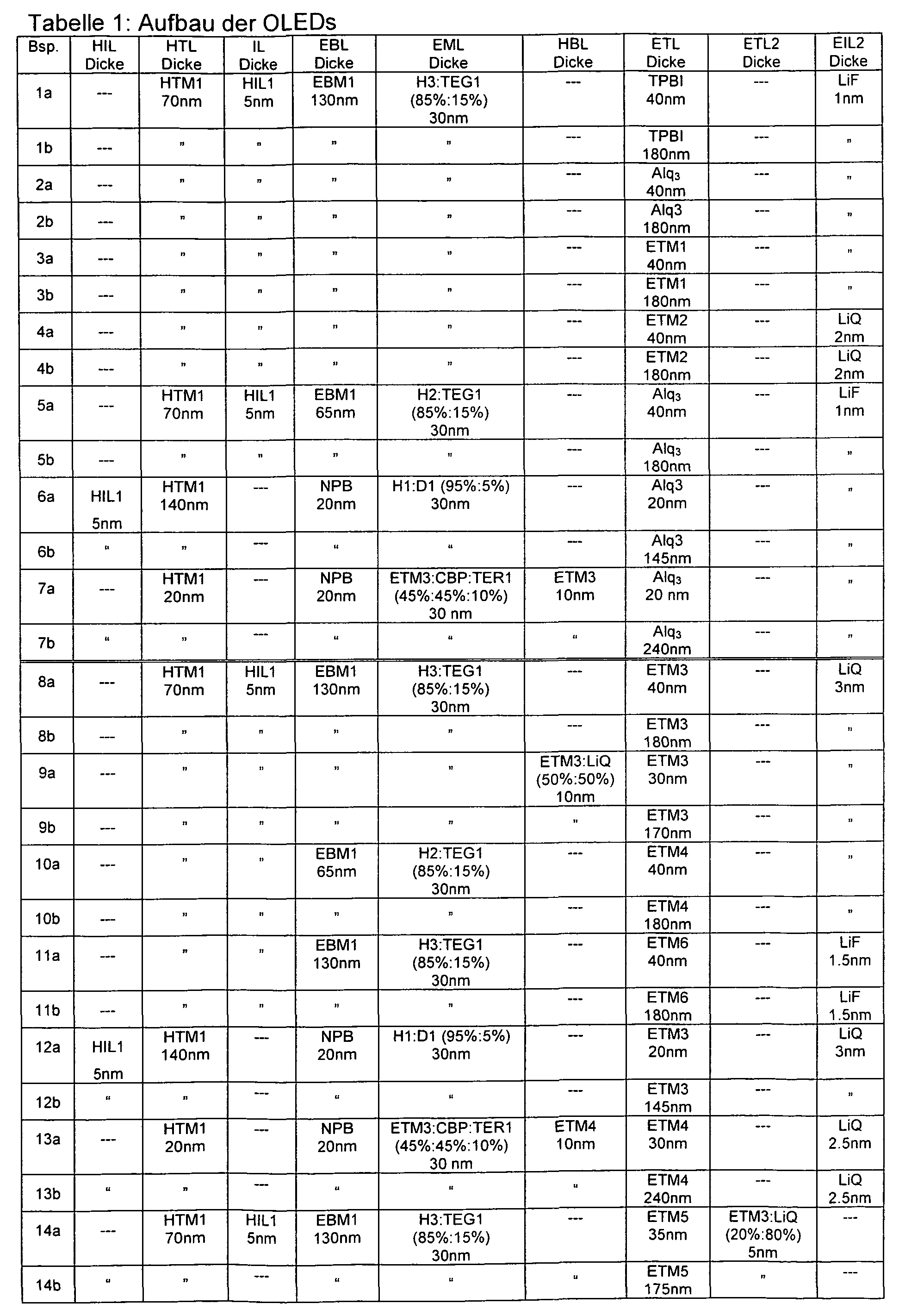
- the OLEDs have in principle the following layer structure: substrate / optional hole injection layer (HIL) / hole transport layer (HTL) / optional intermediate layer (IL) / electron blocker layer (EBL) /
- HIL hole injection layer
- HTL hole transport layer
- IL optional intermediate layer
- EBL electron blocker layer
- Emission Layer Emission Layer
- HBL Optional Hole Blocking Layer
- ETL2 Electron transport layer
- EIL electron injection layer
- Table 1 The exact layer structure of the OLEDs is shown in Table 1.
- Table 3 The materials used to make the OLEDs are shown in Table 3, Table 2 shows the electron mobility of the electron transport materials used at an electric field of 10 5 V / cm (to determine the
- Mobility see Example 1 When using the materials TPBI, Alq 3 , ETM1 and ETM2 in the electron transport layer to obtain OLEDs according to the prior art, while using ETM3 to ETM6 in thick layers components according to the invention are obtained.
- the performance data of the OLEDs are summarized in Table 4.
- the examples are subdivided into “a” and “b” for clarity, with all examples ending in “a” being thin and all ending in “b” contain thick electron transport layers.
- Examples 1-7 both “a” and “b" are prior art OLEDs.
- Examples 8-14 ending with "a” which contain thin electron-transport layers and serve as a comparison with the OLEDs according to the invention
- the OLEDs according to the invention are Examples 8-14 ending in “b” since materials having a correspondingly high molecular weight are used Electron mobility can be used in correspondingly thick electron transport layers.
- the electron transport layer thickness is optimized to obtain good performance data. This applies to the OLEDs with both thin and thick electron transport layers. In the following, therefore, components optimized with respect to the ETL thickness are compared.
- the emission layer always consists of at least one matrix material (host material, host material) and an emitting dopant (dopant, emitter), which is admixed to the matrix material or the matrix materials by co-evaporation in a specific volume fraction.
- the electron transport layer may consist of a mixture of two materials.
- the OLEDs are characterized by default.
- the lifetime is defined as the time after which the luminance has dropped to a certain level from a certain starting luminance.
- LD80 means that the said lifetime is the time at which the luminance dropped to 80% of the starting luminance is, so from z. B. 4000 cd / m 2 to 3200 cd / m 2 .
- LD50 would be the time after which the starting luminance has dropped to half.
- the values for the lifetime can be known with the aid of those skilled in the art
- Conversion formulas are converted to an indication for other starting luminance densities.
- the OLEDs according to the invention are characterized in that they provide improved color coordinates and a reduced number of short circuits, wherein power efficiency and lifetime are at the same level as in the case of thin electron transport layers (Examples 7a, 7b and 13a and 13b, 13b the inventive OLED is).
- Electron transport layers in OLEDs that show green phosphorescence This is due to the fact that the emission spectrum becomes narrower when correspondingly thicker emission layers are used. In the case of blue and red emission, this results in only slight improvements in the color coordinates, in the green spectral range, this effect is more pronounced. Furthermore, in the case of green emission, a clearer increase in the current efficiency can be achieved, with the result that with electron-transport layers according to the invention even better power efficiencies can be achieved despite somewhat higher operating voltages than with thin ETLs.
- Examples 1a and 11b are mentioned which show a significant increase of 10% in the power efficiency when using an ETL according to the invention.
Abstract
Description


Claims
Priority Applications (4)
| Application Number | Priority Date | Filing Date | Title |
|---|---|---|---|
| CN201080041123XA CN102498587A (en) | 2009-09-16 | 2010-08-16 | Organic electroluminescent device |
| US13/395,476 US20120168735A1 (en) | 2009-09-16 | 2010-08-16 | Organic electroluminescent device |
| KR1020177011113A KR20170048611A (en) | 2009-09-16 | 2010-08-16 | Organic electroluminescent device |
| JP2012529134A JP2013504882A (en) | 2009-09-16 | 2010-08-16 | Organic electroluminescence device |
Applications Claiming Priority (2)
| Application Number | Priority Date | Filing Date | Title |
|---|---|---|---|
| DE102009041289A DE102009041289A1 (en) | 2009-09-16 | 2009-09-16 | Organic electroluminescent device |
| DE102009041289.1 | 2009-09-16 |
Publications (1)
| Publication Number | Publication Date |
|---|---|
| WO2011032624A1 true WO2011032624A1 (en) | 2011-03-24 |
Family
ID=43398288
Family Applications (1)
| Application Number | Title | Priority Date | Filing Date |
|---|---|---|---|
| PCT/EP2010/005022 WO2011032624A1 (en) | 2009-09-16 | 2010-08-16 | Organic electroluminescent device |
Country Status (7)
| Country | Link |
|---|---|
| US (1) | US20120168735A1 (en) |
| JP (2) | JP2013504882A (en) |
| KR (2) | KR20170048611A (en) |
| CN (2) | CN102498587A (en) |
| DE (1) | DE102009041289A1 (en) |
| TW (1) | TW201129245A (en) |
| WO (1) | WO2011032624A1 (en) |
Cited By (3)
| Publication number | Priority date | Publication date | Assignee | Title |
|---|---|---|---|---|
| WO2018069167A1 (en) | 2016-10-10 | 2018-04-19 | Merck Patent Gmbh | Electronic device |
| WO2020225071A1 (en) | 2019-05-03 | 2020-11-12 | Merck Patent Gmbh | Electronic device |
| WO2020225069A1 (en) | 2019-05-03 | 2020-11-12 | Merck Patent Gmbh | Electronic device |
Families Citing this family (23)
| Publication number | Priority date | Publication date | Assignee | Title |
|---|---|---|---|---|
| DE102009041289A1 (en) * | 2009-09-16 | 2011-03-17 | Merck Patent Gmbh | Organic electroluminescent device |
| KR102084170B1 (en) * | 2013-07-25 | 2020-03-04 | 삼성디스플레이 주식회사 | An organic light emitting device, an organic light emitting display appratus having the organic light emitting device and a method of manufacturing the same |
| JP2015082537A (en) * | 2013-10-22 | 2015-04-27 | コニカミノルタ株式会社 | Organic electroluminescent element, method of manufacturing the same, and organic electroluminescent device |
| KR20150108330A (en) * | 2014-03-17 | 2015-09-25 | 롬엔드하스전자재료코리아유한회사 | Electron buffering material and organic electroluminescent device comprising the same |
| KR101537500B1 (en) * | 2014-04-04 | 2015-07-20 | 주식회사 엘지화학 | Organic light emitting diode |
| CN113527032A (en) * | 2014-04-16 | 2021-10-22 | 默克专利有限公司 | Material for electronic devices |
| WO2016012221A2 (en) * | 2014-07-21 | 2016-01-28 | Cynora Gmbh | Organic component |
| KR101536569B1 (en) * | 2014-08-01 | 2015-07-14 | 선문대학교 산학협력단 | Blue phosphorescent organic light emitting diode device having improved efficiency by controlling recombination zone spatially |
| JP6815294B2 (en) | 2016-09-30 | 2021-01-20 | 株式会社Joled | Organic EL element and organic EL panel |
| EP3358639B1 (en) * | 2017-01-16 | 2022-04-06 | Samsung Electronics Co., Ltd. | Organic light-emitting device |
| US11393987B2 (en) | 2017-03-01 | 2022-07-19 | Merck Patent Gmbh | Organic electroluminescent device |
| KR102513175B1 (en) | 2017-04-27 | 2023-03-24 | 스미또모 가가꾸 가부시키가이샤 | Composition and light emitting device using the same |
| KR20190070586A (en) * | 2017-12-13 | 2019-06-21 | 엘지디스플레이 주식회사 | Compound for electron transporting material and organic light emitting diode including the same |
| KR102027523B1 (en) | 2017-12-22 | 2019-10-01 | 엘지디스플레이 주식회사 | Organic light emitting diode and organic light emittind display device having the same |
| KR102027516B1 (en) * | 2017-12-22 | 2019-10-01 | 엘지디스플레이 주식회사 | Organic light emitting diode and organic light emittind display device having the same |
| KR102027518B1 (en) | 2017-12-22 | 2019-10-01 | 엘지디스플레이 주식회사 | Organic light emitting diode and organic light emittind display device having the same |
| EP3582280B1 (en) * | 2018-06-14 | 2024-03-20 | Novaled GmbH | Organic material for an electronic optoelectronic device and electronic device comprising the organic material |
| EP3799142A4 (en) * | 2018-08-24 | 2021-07-28 | Lg Chem, Ltd. | Organic light emitting diode |
| CN109326735B (en) | 2018-09-30 | 2021-01-01 | 云谷(固安)科技有限公司 | Organic light-emitting diode, display panel and display device |
| KR102150870B1 (en) * | 2019-09-25 | 2020-09-02 | 엘지디스플레이 주식회사 | Organic light emitting diode and organic light emittind display device having the same |
| KR102332549B1 (en) * | 2019-09-25 | 2021-12-01 | 엘지디스플레이 주식회사 | Organic light emitting diode and organic light emittind display device having the same |
| CN110911574A (en) * | 2019-11-29 | 2020-03-24 | 昆山国显光电有限公司 | Composition, OLED device, OLED display panel and display device |
| WO2023142983A1 (en) * | 2022-01-27 | 2023-08-03 | 浙江光昊光电科技有限公司 | Azacarbene carbon free radical molecule, mixture and composition comprising same, and use thereof in organic electronic device |
Citations (76)
| Publication number | Priority date | Publication date | Assignee | Title |
|---|---|---|---|---|
| US4539507A (en) | 1983-03-25 | 1985-09-03 | Eastman Kodak Company | Organic electroluminescent devices having improved power conversion efficiencies |
| US4780536A (en) | 1986-09-05 | 1988-10-25 | The Ohio State University Research Foundation | Hexaazatriphenylene hexanitrile and its derivatives and their preparations |
| US5061569A (en) | 1990-07-26 | 1991-10-29 | Eastman Kodak Company | Electroluminescent device with organic electroluminescent medium |
| US5151629A (en) | 1991-08-01 | 1992-09-29 | Eastman Kodak Company | Blue emitting internal junction organic electroluminescent device (I) |
| WO1995009147A1 (en) | 1993-09-29 | 1995-04-06 | Idemitsu Kosan Co., Ltd. | Organic electroluminescent element and arylenediamine derivative |
| EP0650955A1 (en) | 1993-11-01 | 1995-05-03 | Hodogaya Chemical Co., Ltd. | Amine compound and electro-luminescence device comprising same |
| EP0652273A1 (en) | 1993-11-09 | 1995-05-10 | Shinko Electric Industries Co. Ltd. | Organic material for electroluminescent device and electroluminescent device |
| EP0676461A2 (en) | 1994-04-07 | 1995-10-11 | Hoechst Aktiengesellschaft | Spiro compounds and their application as electroluminescence materials |
| WO1998027136A1 (en) | 1996-12-16 | 1998-06-25 | Aventis Research & Technologies Gmbh & Co Kg | ARYL-SUBSTITUTED POLY(p-ARYLENE VINYLENES), METHOD FOR THE PRODUCTION AND USE THEREOF IN ELECTROLUMINESCENT COMPONENTS |
| WO1998030071A1 (en) | 1996-12-28 | 1998-07-09 | Tdk Corporation | Organic electroluminescent elements |
| WO2000070655A2 (en) | 1999-05-13 | 2000-11-23 | The Trustees Of Princeton University | Very high efficiency organic light emitting devices based on electrophosphorescence |
| WO2001041512A1 (en) | 1999-12-01 | 2001-06-07 | The Trustees Of Princeton University | Complexes of form l2mx as phosphorescent dopants for organic leds |
| WO2001049806A1 (en) | 1999-12-31 | 2001-07-12 | Lg Chemical Co., Ltd | Electronic device comprising organic compound having p-type semiconducting characteristics |
| JP2001226331A (en) | 2000-02-14 | 2001-08-21 | Mitsui Chemicals Inc | Amine compound and organic electroluminescent element containing the compound |
| EP1144543A1 (en) | 1998-12-02 | 2001-10-17 | South Bank University Enterprises Ltd. | Electroluminescent quinolates |
| WO2002002714A2 (en) | 2000-06-30 | 2002-01-10 | E.I. Du Pont De Nemours And Company | Electroluminescent iridium compounds with fluorinated phenylpyridines, phenylpyrimidines, and phenylquinolines and devices made with such compounds |
| WO2002015645A1 (en) | 2000-08-11 | 2002-02-21 | The Trustees Of Princeton University | Organometallic compounds and emission-shifting organic electrophosphorescence |
| EP1191613A2 (en) | 2000-09-26 | 2002-03-27 | Canon Kabushiki Kaisha | Luminescence device, display apparatus and metal coordination compound |
| EP1191612A2 (en) | 2000-09-26 | 2002-03-27 | Canon Kabushiki Kaisha | Luminescence device, display apparatus and metal coordination compound |
| EP1191614A2 (en) | 2000-09-26 | 2002-03-27 | Canon Kabushiki Kaisha | Luminescence device and metal coordination compound therefor |
| EP1205527A1 (en) | 2000-03-27 | 2002-05-15 | Idemitsu Kosan Co., Ltd. | Organic electroluminescence device |
| WO2004013080A1 (en) | 2002-08-01 | 2004-02-12 | Covion Organic Semiconductors Gmbh | Spirobifluorene derivatives, their preparation and uses thereof |
| WO2004058911A2 (en) | 2002-12-23 | 2004-07-15 | Covion Organic Semiconductors Gmbh | Organic electroluminescent element |
| WO2004081017A1 (en) | 2003-03-11 | 2004-09-23 | Covion Organic Semiconductors Gmbh | Metal complexes |
| JP2004288381A (en) | 2003-03-19 | 2004-10-14 | Konica Minolta Holdings Inc | Organic electroluminescent element |
| WO2004093207A2 (en) | 2003-04-15 | 2004-10-28 | Covion Organic Semiconductors Gmbh | Mixtures of matrix materials and organic semiconductors capable of emission, use of the same and electronic components containing said mixtures |
| WO2005011013A1 (en) | 2003-07-21 | 2005-02-03 | Covion Organic Semiconductors Gmbh | Organic electroluminescent element |
| US20050069729A1 (en) | 2003-09-30 | 2005-03-31 | Konica Minolta Holdings, Inc. | Organic electroluminescent element, illuminator, display and compound |
| WO2005033244A1 (en) | 2003-09-29 | 2005-04-14 | Covion Organic Semiconductors Gmbh | Metal complexes |
| WO2005042550A1 (en) | 2003-10-30 | 2005-05-12 | Merck Patent Gmbh | Metal complexes with bipodal ligands |
| WO2005084081A1 (en) | 2004-02-20 | 2005-09-09 | Merck Patent Gmbh | Organic electronic devices |
| WO2005111172A2 (en) | 2004-05-11 | 2005-11-24 | Merck Patent Gmbh | Novel material mixtures for use in electroluminescence |
| WO2005113563A1 (en) | 2004-05-19 | 2005-12-01 | Merck Patent Gmbh | Metal complexes |
| JP2005347160A (en) | 2004-06-04 | 2005-12-15 | Konica Minolta Holdings Inc | Organic electroluminescent element, lighting device, and display device |
| WO2006000389A1 (en) | 2004-06-26 | 2006-01-05 | Merck Patent Gmbh | Compounds for organic electronic devices |
| WO2006000388A1 (en) | 2004-06-26 | 2006-01-05 | Merck Patent Gmbh | Organic electroluminescent device |
| EP1617711A1 (en) | 2003-04-23 | 2006-01-18 | Konica Minolta Holdings, Inc. | Organic electroluminescent device and display |
| WO2006005627A1 (en) | 2004-07-15 | 2006-01-19 | Merck Patent Gmbh | Oligomeric derivatives of spirobifluorene, their preparation and use |
| WO2006008069A1 (en) | 2004-07-16 | 2006-01-26 | Merck Patent Gmbh | Metal complexes |
| WO2006048268A1 (en) | 2004-11-06 | 2006-05-11 | Merck Patent Gmbh | Organic electroluminescent device |
| EP1661888A1 (en) | 2004-11-29 | 2006-05-31 | Samsung SDI Co., Ltd. | Phenylcarbazole-based compound and organic electroluminescent device employing the same |
| WO2006058737A1 (en) | 2004-12-01 | 2006-06-08 | Merck Patent Gmbh | Compounds for organic electronic devices |
| WO2006061182A1 (en) | 2004-12-09 | 2006-06-15 | Merck Patent Gmbh | Metal complexes and their use as the emitting constituent in electronic components, in particular in electroluminescent display devices |
| WO2006073054A1 (en) | 2005-01-05 | 2006-07-13 | Idemitsu Kosan Co., Ltd. | Aromatic amine derivative and organic electroluminescent device using same |
| WO2006081973A1 (en) | 2005-02-03 | 2006-08-10 | Merck Patent Gmbh | Metal complexes |
| JP2006253445A (en) | 2005-03-11 | 2006-09-21 | Toyo Ink Mfg Co Ltd | Organic electroluminescence element |
| WO2006100896A1 (en) | 2005-03-18 | 2006-09-28 | Idemitsu Kosan Co., Ltd. | Aromatic amine derivative and organic electroluminescence device utilizing the same |
| WO2006117052A1 (en) | 2005-05-03 | 2006-11-09 | Merck Patent Gmbh | Organic electroluminescent device and boric acid and borinic acid derivatives used therein |
| WO2006122630A1 (en) | 2005-05-20 | 2006-11-23 | Merck Patent Gmbh | Compounds for organic electronic devices |
| EP1731584A1 (en) | 2004-03-31 | 2006-12-13 | Konica Minolta Holdings, Inc. | Organic electroluminescent device material, organic electroluminescent device, display and illuminating device |
| WO2007050301A2 (en) | 2005-10-26 | 2007-05-03 | Eastman Kodak Company | Organic element for low voltage electroluminescent devices |
| WO2007050334A1 (en) | 2005-10-26 | 2007-05-03 | Eastman Kodak Company | Organic element for low voltage electroluminescent devices |
| WO2007063754A1 (en) | 2005-12-01 | 2007-06-07 | Nippon Steel Chemical Co., Ltd. | Compound for organic electroluminescent element and organic electroluminescent element |
| WO2007065549A1 (en) | 2005-12-08 | 2007-06-14 | Merck Patent Gmbh | Organic electroluminescent devices |
| WO2007115610A1 (en) | 2006-04-01 | 2007-10-18 | Merck Patent Gmbh | Materials for organic electroluminescent devices |
| WO2007137725A1 (en) | 2006-05-31 | 2007-12-06 | Merck Patent Gmbh | New materials for organic electroluminescent devices |
| WO2007140847A1 (en) | 2006-06-02 | 2007-12-13 | Merck Patent Gmbh | Materials for organic electroluminescent devices |
| WO2008006449A1 (en) | 2006-07-11 | 2008-01-17 | Merck Patent Gmbh | Novel materials for organic electroluminescent devices |
| WO2008056746A1 (en) | 2006-11-09 | 2008-05-15 | Nippon Steel Chemical Co., Ltd. | Compound for organic electroluminescent device and organic electroluminescent device |
| WO2008086851A1 (en) | 2007-01-18 | 2008-07-24 | Merck Patent Gmbh | Carbazole derivatives for organc electroluminescent devices |
| US20080233387A1 (en) * | 2007-03-07 | 2008-09-25 | Sony Corporation | Organic electroluminescent device and display device |
| EP1978576A2 (en) * | 2007-04-03 | 2008-10-08 | Fujikura, Ltd. | Organic light-emitting diode element and optical interconnection module |
| WO2008145239A2 (en) | 2007-05-29 | 2008-12-04 | Merck Patent Gmbh | Benzanthracene derivatives for organic electroluminescent devices |
| WO2009062578A1 (en) | 2007-11-12 | 2009-05-22 | Merck Patent Gmbh | Organic electroluminescent devices comprising azomethine-metal complexes |
| US20090136779A1 (en) | 2007-11-26 | 2009-05-28 | Chien-Hong Cheng | Conjugated compounds containing hydroindoloacridine structural elements, and their use |
| US20090134784A1 (en) | 2004-10-21 | 2009-05-28 | Universal Display Corporation | Carbazole-containing materials in phosphorescent light emitting diodes |
| US20090167156A1 (en) * | 2007-02-28 | 2009-07-02 | Idemitsu Kosan Co., Ltd. | Organic electroluminescence device |
| WO2009118087A1 (en) | 2008-03-25 | 2009-10-01 | Merck Patent Gmbh | Metal complexes |
| WO2009148015A1 (en) | 2008-06-05 | 2009-12-10 | 出光興産株式会社 | Halogen compound, polycyclic compound, and organic electroluminescence element comprising the polycyclic compound |
| WO2009146770A2 (en) | 2008-06-05 | 2009-12-10 | Merck Patent Gmbh | Electronic device comprising metal complexes |
| WO2010006680A1 (en) | 2008-07-18 | 2010-01-21 | Merck Patent Gmbh | Materials for organic electroluminescence devices |
| WO2010012328A1 (en) | 2008-07-29 | 2010-02-04 | Merck Patent Gmbh | Compounds for electronic devices |
| WO2010015306A1 (en) | 2008-08-08 | 2010-02-11 | Merck Patent Gmbh, | Organic electroluminescence device |
| WO2010050778A1 (en) | 2008-10-31 | 2010-05-06 | Gracel Display Inc. | Novel compounds for organic electronic material and organic electronic device using the same |
| WO2010054729A2 (en) | 2008-11-11 | 2010-05-20 | Merck Patent Gmbh | Materials for organic electroluminescence devices |
| WO2010054730A1 (en) | 2008-11-11 | 2010-05-20 | Merck Patent Gmbh | Organic electroluminescent devices |
Family Cites Families (108)
| Publication number | Priority date | Publication date | Assignee | Title |
|---|---|---|---|---|
| TW421668B (en) * | 1994-05-26 | 2001-02-11 | Sumitomo Electric Industries | Organic electroluminescent device |
| US6229012B1 (en) * | 1998-10-01 | 2001-05-08 | Xerox Corporation | Triazine compositions |
| US6225467B1 (en) * | 2000-01-21 | 2001-05-01 | Xerox Corporation | Electroluminescent (EL) devices |
| US6821643B1 (en) * | 2000-01-21 | 2004-11-23 | Xerox Corporation | Electroluminescent (EL) devices |
| JP4040249B2 (en) * | 2000-11-16 | 2008-01-30 | 富士フイルム株式会社 | Light emitting element |
| JP4302901B2 (en) * | 2001-02-27 | 2009-07-29 | 三星モバイルディスプレイ株式會社 | Luminescent body and light emitting system |
| US7749818B2 (en) * | 2002-01-28 | 2010-07-06 | Semiconductor Energy Laboratory Co., Ltd. | Semiconductor device and method of manufacturing the same |
| JP2003226870A (en) * | 2002-02-04 | 2003-08-15 | Matsushita Electric Ind Co Ltd | Luminescent element material and luminescent element and device produced by using the material |
| JP4443872B2 (en) * | 2002-08-09 | 2010-03-31 | 株式会社半導体エネルギー研究所 | Electroluminescent device, light emitting device, electric appliance |
| US7045955B2 (en) * | 2002-08-09 | 2006-05-16 | Semiconductor Energy Laboratory Co., Ltd. | Electroluminescence element and a light emitting device using the same |
| US7161291B2 (en) * | 2002-09-24 | 2007-01-09 | Dai Nippon Printing Co., Ltd | Display element and method for producing the same |
| JP4066802B2 (en) * | 2002-12-17 | 2008-03-26 | 富士ゼロックス株式会社 | POLYESTER RESIN AND FUNCTIONAL DEVICE USING SAME, ORGANIC ELECTROLUMINESCENT DEVICE, AND METHOD FOR PRODUCING ORGANIC ELECTROLUMINESCENT DEVICE |
| JP2004277377A (en) * | 2003-03-18 | 2004-10-07 | Junji Kido | Fluorene compound and organic electroluminescent element produced by using the same |
| US7371469B2 (en) * | 2003-07-08 | 2008-05-13 | Konica Minolta Holdings, Inc. | Organic electroluminescent element, illuminator and display |
| US20050025993A1 (en) * | 2003-07-25 | 2005-02-03 | Thompson Mark E. | Materials and structures for enhancing the performance of organic light emitting devices |
| JP4961412B2 (en) * | 2003-11-10 | 2012-06-27 | 淳二 城戸 | ORGANIC ELEMENT AND METHOD FOR PRODUCING ORGANIC ELEMENT |
| DE10356099A1 (en) * | 2003-11-27 | 2005-07-07 | Covion Organic Semiconductors Gmbh | Organic electroluminescent element |
| US7157155B2 (en) * | 2004-01-09 | 2007-01-02 | The University Of Hong Kong | Materials for electroluminescent devices |
| EP2325190B1 (en) * | 2004-03-11 | 2013-05-08 | Mitsubishi Chemical Corporation | Composition for charge-transporting film and ion compound, charge-transporting film and organic electroluminescent device using same |
| JPWO2006008976A1 (en) * | 2004-07-16 | 2008-05-01 | コニカミノルタホールディングス株式会社 | White light-emitting organic electroluminescence element, display device, and illumination device |
| JP2006073641A (en) * | 2004-08-31 | 2006-03-16 | Sanyo Electric Co Ltd | Organic electroluminescence element and organic electroluminescnece device having the same |
| JP2006086284A (en) * | 2004-09-15 | 2006-03-30 | Tosoh Corp | Electron transfer material made of 1,3,5-triazine derivative |
| US7803468B2 (en) * | 2004-09-29 | 2010-09-28 | Fujifilm Corporation | Organic electroluminescent element |
| JP4969086B2 (en) * | 2004-11-17 | 2012-07-04 | 富士フイルム株式会社 | Organic electroluminescence device |
| US20060194077A1 (en) * | 2005-02-28 | 2006-08-31 | Fuji Photo Film Co., Ltd. | Organic light emitting diode and display using the same |
| JP2006253015A (en) * | 2005-03-11 | 2006-09-21 | Idemitsu Kosan Co Ltd | Organic electroluminescence color light-emitting device |
| US7777407B2 (en) * | 2005-05-04 | 2010-08-17 | Lg Display Co., Ltd. | Organic light emitting devices comprising a doped triazine electron transport layer |
| US7429662B2 (en) * | 2005-05-20 | 2008-09-30 | City University Of Hong Kong | Red-emitting electrophosphorescent devices |
| FR2887665B1 (en) * | 2005-06-27 | 2007-10-12 | Oberthur Card Syst Sa | ELECTRONIC ENTITY WITH MAGNETIC ANTENNA |
| KR100806812B1 (en) * | 2005-07-25 | 2008-02-25 | 엘지.필립스 엘시디 주식회사 | Organic Electroluminescence Device and method for fabricating the same |
| US7872411B2 (en) * | 2005-08-17 | 2011-01-18 | Showa Denko K.K. | Organic electroluminescence device using a copolymer and a phosphorescent compound |
| US20100301310A1 (en) * | 2005-10-07 | 2010-12-02 | Sumitomo Chemical Company, Limited | Polymer and polymeric luminescent element employing the same |
| JP2007141736A (en) * | 2005-11-21 | 2007-06-07 | Fujifilm Corp | Organic electroluminescent element |
| KR100991347B1 (en) * | 2005-12-22 | 2010-11-01 | 쇼와 덴코 가부시키가이샤 | Organic light-emitting device |
| JP2007200938A (en) * | 2006-01-23 | 2007-08-09 | Fujifilm Corp | Organic electroluminescence light emitting device |
| US20070182321A1 (en) * | 2006-02-09 | 2007-08-09 | Fujifilm Corporation | Organic electroluminescence device and producing method therefor |
| JP5095948B2 (en) * | 2006-02-22 | 2012-12-12 | 東ソー株式会社 | Terphenylyl-1,3,5-triazine derivative, process for producing the same, and organic electroluminescent device comprising the same |
| JP4896544B2 (en) * | 2006-03-06 | 2012-03-14 | 富士フイルム株式会社 | Organic electroluminescence device |
| KR101386215B1 (en) * | 2006-06-07 | 2014-04-17 | 삼성디스플레이 주식회사 | Compositions of conducting polymers and the organic opto-electronic device employing the same |
| WO2007145129A1 (en) * | 2006-06-13 | 2007-12-21 | Konica Minolta Holdings, Inc. | Organic electroluminescent device, illuminating device and display |
| JP4909695B2 (en) * | 2006-09-27 | 2012-04-04 | 富士フイルム株式会社 | Organic electroluminescence device |
| US20080180023A1 (en) * | 2006-09-28 | 2008-07-31 | Fujifilm Corporation | Organic electroluminescence element |
| JP5342103B2 (en) * | 2006-10-16 | 2013-11-13 | 昭和電工株式会社 | Organic light emitting device |
| JP2008130840A (en) * | 2006-11-21 | 2008-06-05 | Tosoh Corp | Organic electroluminescent element |
| JP2008146904A (en) * | 2006-12-07 | 2008-06-26 | Sony Corp | Organic electroluminescent element and display device |
| US20080135804A1 (en) * | 2006-12-08 | 2008-06-12 | Chunong Qiu | All-in-one organic electroluminescent inks with balanced charge transport properties |
| US8299787B2 (en) * | 2006-12-18 | 2012-10-30 | Konica Minolta Holdings, Inc. | Multicolor phosphorescent organic electroluminescent element and lighting system |
| JP5281801B2 (en) * | 2007-02-01 | 2013-09-04 | 住友化学株式会社 | Block copolymer and polymer light emitting device |
| JP2008218986A (en) * | 2007-02-06 | 2008-09-18 | Sumitomo Chemical Co Ltd | Composition and light-emitting element using the same |
| JP5117199B2 (en) * | 2007-02-13 | 2013-01-09 | 富士フイルム株式会社 | Organic electroluminescence device |
| KR100858816B1 (en) * | 2007-03-14 | 2008-09-17 | 삼성에스디아이 주식회사 | Organic light emitting device comprising anthracene derivative compound |
| JP2008277799A (en) * | 2007-04-03 | 2008-11-13 | Fujikura Ltd | Organic electroluminescent element and module for optical communication |
| JP2008276212A (en) * | 2007-04-05 | 2008-11-13 | Fujifilm Corp | Organic electroluminescent display device |
| US20080284318A1 (en) * | 2007-05-17 | 2008-11-20 | Deaton Joseph C | Hybrid fluorescent/phosphorescent oleds |
| US20080286610A1 (en) * | 2007-05-17 | 2008-11-20 | Deaton Joseph C | Hybrid oled with fluorescent and phosphorescent layers |
| WO2009011272A1 (en) * | 2007-07-13 | 2009-01-22 | Showa Denko K.K. | Organic light-emitting device using triazine ring-containing polymer compound |
| EP2178343B2 (en) * | 2007-07-27 | 2020-04-08 | AGC Inc. | Translucent substrate, method for manufacturing the translucent substrate and organic led element |
| JP2009032990A (en) * | 2007-07-27 | 2009-02-12 | Fujifilm Corp | Organic electroluminescent element |
| JP5255794B2 (en) * | 2007-07-27 | 2013-08-07 | ユー・ディー・シー アイルランド リミテッド | Organic electroluminescence device |
| JP2009037981A (en) * | 2007-08-03 | 2009-02-19 | Idemitsu Kosan Co Ltd | Organic el device and manufacturing method for organic el device |
| JP5452853B2 (en) * | 2007-08-28 | 2014-03-26 | パナソニック株式会社 | Organic electroluminescence device |
| JP2009087744A (en) * | 2007-09-28 | 2009-04-23 | Dainippon Printing Co Ltd | Light-emitting element |
| JP2009087760A (en) * | 2007-09-28 | 2009-04-23 | Dainippon Printing Co Ltd | Manufacturing method of electroluminescent element |
| KR100879477B1 (en) * | 2007-10-11 | 2009-01-20 | 삼성모바일디스플레이주식회사 | Organic light emitting device |
| JP4915356B2 (en) * | 2008-01-29 | 2012-04-11 | セイコーエプソン株式会社 | LIGHT EMITTING ELEMENT, DISPLAY DEVICE, AND ELECTRONIC DEVICE |
| US20090208776A1 (en) * | 2008-02-19 | 2009-08-20 | General Electric Company | Organic optoelectronic device and method for manufacturing the same |
| JP2009211892A (en) * | 2008-03-03 | 2009-09-17 | Fujifilm Corp | Organic electroluminescent element |
| JP5593621B2 (en) * | 2008-04-03 | 2014-09-24 | ソニー株式会社 | Organic electroluminescence device and display device |
| JP2008187205A (en) * | 2008-04-28 | 2008-08-14 | Idemitsu Kosan Co Ltd | Organic electroluminescent element and display unit using the same |
| KR20110018376A (en) * | 2008-06-23 | 2011-02-23 | 스미또모 가가꾸 가부시키가이샤 | Composition and light-emitting element using the composition |
| JP5625272B2 (en) * | 2008-07-29 | 2014-11-19 | 住友化学株式会社 | Compound containing 1,3-diene and method for producing the same |
| DE102008044868A1 (en) * | 2008-08-29 | 2010-03-04 | Merck Patent Gmbh | Electroluminescent polymers, process for their preparation and their use |
| DE102008045663A1 (en) * | 2008-09-03 | 2010-03-04 | Merck Patent Gmbh | Fluorine-bridged associates for opto-electronic applications |
| JP2012502303A (en) * | 2008-09-09 | 2012-01-26 | メルク パテント ゲゼルシャフト ミット ベシュレンクテル ハフツング | Organic materials and electrophotographic equipment |
| WO2010045606A1 (en) * | 2008-10-17 | 2010-04-22 | Bloominescence, Inc. | Transparent polarized light-emitting device |
| JP5293120B2 (en) * | 2008-11-28 | 2013-09-18 | 住友化学株式会社 | Organic electroluminescence device and method for producing the same |
| US9797567B2 (en) * | 2008-12-11 | 2017-10-24 | Osram Oled Gmbh | Organic-light-emitting diode and luminaire |
| US8278651B2 (en) * | 2008-12-22 | 2012-10-02 | E I Du Pont De Nemours And Company | Electronic device including 1,7-phenanthroline derivative |
| DE102008064200A1 (en) * | 2008-12-22 | 2010-07-01 | Merck Patent Gmbh | Organic electroluminescent device |
| JP5551428B2 (en) * | 2009-01-06 | 2014-07-16 | ユー・ディー・シー アイルランド リミテッド | Charge transport material and organic electroluminescent device |
| DE102009005290A1 (en) | 2009-01-20 | 2010-07-22 | Merck Patent Gmbh | Connections for electronic devices |
| KR20110117063A (en) * | 2009-01-23 | 2011-10-26 | 도레이 카부시키가이샤 | Light-emitting element material and light-emitting element |
| DE102009005746A1 (en) | 2009-01-23 | 2010-07-29 | Merck Patent Gmbh | Materials for organic electroluminescent devices |
| DE102009007038A1 (en) * | 2009-02-02 | 2010-08-05 | Merck Patent Gmbh | metal complexes |
| DE102009012346B4 (en) * | 2009-03-09 | 2024-02-15 | Merck Patent Gmbh | Organic electroluminescent device and method for producing the same |
| DE102009014513A1 (en) * | 2009-03-23 | 2010-09-30 | Merck Patent Gmbh | Organic electroluminescent device |
| DE102009023155A1 (en) | 2009-05-29 | 2010-12-02 | Merck Patent Gmbh | Materials for organic electroluminescent devices |
| DE102009031021A1 (en) * | 2009-06-30 | 2011-01-05 | Merck Patent Gmbh | Materials for organic electroluminescent devices |
| DE102009034625A1 (en) | 2009-07-27 | 2011-02-03 | Merck Patent Gmbh | New materials for organic electroluminescent devices |
| EP2462203B1 (en) * | 2009-08-04 | 2016-03-02 | Merck Patent GmbH | Electronic devices comprising multi cyclic hydrocarbons |
| DE102009041289A1 (en) * | 2009-09-16 | 2011-03-17 | Merck Patent Gmbh | Organic electroluminescent device |
| DE102009041414A1 (en) * | 2009-09-16 | 2011-03-17 | Merck Patent Gmbh | metal complexes |
| DE102009053645A1 (en) * | 2009-11-17 | 2011-05-19 | Merck Patent Gmbh | Materials for organic electroluminescent device |
| KR101931922B1 (en) * | 2009-09-16 | 2018-12-21 | 메르크 파텐트 게엠베하 | Formulations for the production of electronic devices |
| DE102009048791A1 (en) * | 2009-10-08 | 2011-04-14 | Merck Patent Gmbh | Materials for organic electroluminescent devices |
| DE102009051172A1 (en) * | 2009-10-29 | 2011-05-05 | Merck Patent Gmbh | Materials for electronic devices |
| DE102009052428A1 (en) * | 2009-11-10 | 2011-05-12 | Merck Patent Gmbh | Connection for electronic devices |
| DE102009053382A1 (en) * | 2009-11-14 | 2011-05-19 | Merck Patent Gmbh | Materials for electronic devices |
| DE102009053836A1 (en) * | 2009-11-18 | 2011-05-26 | Merck Patent Gmbh | Materials for organic electroluminescent devices |
| CN102668152A (en) * | 2009-12-23 | 2012-09-12 | 默克专利有限公司 | Compositions comprising polymeric binders |
| DE102010007938A1 (en) * | 2010-02-12 | 2011-10-06 | Merck Patent Gmbh | Electroluminescent polymers, process for their preparation and their use |
| US9627632B2 (en) * | 2010-03-23 | 2017-04-18 | Merck Patent Gmbh | Materials for organic electroluminescent devices |
| DE102010033080A1 (en) * | 2010-08-02 | 2012-02-02 | Merck Patent Gmbh | Polymers with structural units that have electron transport properties |
| US9159930B2 (en) * | 2010-11-26 | 2015-10-13 | Merck Patent Gmbh | Formulations and electronic devices |
| JP6356060B2 (en) * | 2011-03-24 | 2018-07-11 | メルク パテント ゲーエムベーハー | Organic ionic functional materials |
| EP2737553A1 (en) * | 2011-07-25 | 2014-06-04 | Merck Patent GmbH | Copolymers with functionalized side chains |
| DE102011117422A1 (en) * | 2011-10-28 | 2013-05-02 | Merck Patent Gmbh | Hyperbranched polymers, process for their preparation and their use in electronic devices |
| US9695274B2 (en) * | 2012-06-29 | 2017-07-04 | Merck Patent Gmbh | Polymers containing 2,7-pyrene structural units |
-
2009
- 2009-09-16 DE DE102009041289A patent/DE102009041289A1/en active Pending
-
2010
- 2010-08-16 CN CN201080041123XA patent/CN102498587A/en active Pending
- 2010-08-16 KR KR1020177011113A patent/KR20170048611A/en active IP Right Grant
- 2010-08-16 CN CN201610595091.7A patent/CN106058064B/en active Active
- 2010-08-16 WO PCT/EP2010/005022 patent/WO2011032624A1/en active Application Filing
- 2010-08-16 US US13/395,476 patent/US20120168735A1/en not_active Abandoned
- 2010-08-16 JP JP2012529134A patent/JP2013504882A/en active Pending
- 2010-08-16 KR KR1020127009612A patent/KR20120080606A/en active Application Filing
- 2010-09-13 TW TW099130873A patent/TW201129245A/en unknown
-
2015
- 2015-04-08 JP JP2015079212A patent/JP6490480B2/en active Active
Patent Citations (80)
| Publication number | Priority date | Publication date | Assignee | Title |
|---|---|---|---|---|
| US4539507A (en) | 1983-03-25 | 1985-09-03 | Eastman Kodak Company | Organic electroluminescent devices having improved power conversion efficiencies |
| US4780536A (en) | 1986-09-05 | 1988-10-25 | The Ohio State University Research Foundation | Hexaazatriphenylene hexanitrile and its derivatives and their preparations |
| US5061569A (en) | 1990-07-26 | 1991-10-29 | Eastman Kodak Company | Electroluminescent device with organic electroluminescent medium |
| US5151629A (en) | 1991-08-01 | 1992-09-29 | Eastman Kodak Company | Blue emitting internal junction organic electroluminescent device (I) |
| WO1995009147A1 (en) | 1993-09-29 | 1995-04-06 | Idemitsu Kosan Co., Ltd. | Organic electroluminescent element and arylenediamine derivative |
| EP0650955A1 (en) | 1993-11-01 | 1995-05-03 | Hodogaya Chemical Co., Ltd. | Amine compound and electro-luminescence device comprising same |
| EP0652273A1 (en) | 1993-11-09 | 1995-05-10 | Shinko Electric Industries Co. Ltd. | Organic material for electroluminescent device and electroluminescent device |
| EP0676461A2 (en) | 1994-04-07 | 1995-10-11 | Hoechst Aktiengesellschaft | Spiro compounds and their application as electroluminescence materials |
| WO1998027136A1 (en) | 1996-12-16 | 1998-06-25 | Aventis Research & Technologies Gmbh & Co Kg | ARYL-SUBSTITUTED POLY(p-ARYLENE VINYLENES), METHOD FOR THE PRODUCTION AND USE THEREOF IN ELECTROLUMINESCENT COMPONENTS |
| WO1998030071A1 (en) | 1996-12-28 | 1998-07-09 | Tdk Corporation | Organic electroluminescent elements |
| EP0891121A1 (en) | 1996-12-28 | 1999-01-13 | TDK Corporation | Organic electroluminescent elements |
| EP1144543A1 (en) | 1998-12-02 | 2001-10-17 | South Bank University Enterprises Ltd. | Electroluminescent quinolates |
| WO2000070655A2 (en) | 1999-05-13 | 2000-11-23 | The Trustees Of Princeton University | Very high efficiency organic light emitting devices based on electrophosphorescence |
| WO2001041512A1 (en) | 1999-12-01 | 2001-06-07 | The Trustees Of Princeton University | Complexes of form l2mx as phosphorescent dopants for organic leds |
| WO2001049806A1 (en) | 1999-12-31 | 2001-07-12 | Lg Chemical Co., Ltd | Electronic device comprising organic compound having p-type semiconducting characteristics |
| JP2001226331A (en) | 2000-02-14 | 2001-08-21 | Mitsui Chemicals Inc | Amine compound and organic electroluminescent element containing the compound |
| EP1205527A1 (en) | 2000-03-27 | 2002-05-15 | Idemitsu Kosan Co., Ltd. | Organic electroluminescence device |
| WO2002002714A2 (en) | 2000-06-30 | 2002-01-10 | E.I. Du Pont De Nemours And Company | Electroluminescent iridium compounds with fluorinated phenylpyridines, phenylpyrimidines, and phenylquinolines and devices made with such compounds |
| WO2002015645A1 (en) | 2000-08-11 | 2002-02-21 | The Trustees Of Princeton University | Organometallic compounds and emission-shifting organic electrophosphorescence |
| EP1191614A2 (en) | 2000-09-26 | 2002-03-27 | Canon Kabushiki Kaisha | Luminescence device and metal coordination compound therefor |
| EP1191612A2 (en) | 2000-09-26 | 2002-03-27 | Canon Kabushiki Kaisha | Luminescence device, display apparatus and metal coordination compound |
| EP1191613A2 (en) | 2000-09-26 | 2002-03-27 | Canon Kabushiki Kaisha | Luminescence device, display apparatus and metal coordination compound |
| WO2004013080A1 (en) | 2002-08-01 | 2004-02-12 | Covion Organic Semiconductors Gmbh | Spirobifluorene derivatives, their preparation and uses thereof |
| WO2004058911A2 (en) | 2002-12-23 | 2004-07-15 | Covion Organic Semiconductors Gmbh | Organic electroluminescent element |
| WO2004081017A1 (en) | 2003-03-11 | 2004-09-23 | Covion Organic Semiconductors Gmbh | Metal complexes |
| JP2004288381A (en) | 2003-03-19 | 2004-10-14 | Konica Minolta Holdings Inc | Organic electroluminescent element |
| WO2004093207A2 (en) | 2003-04-15 | 2004-10-28 | Covion Organic Semiconductors Gmbh | Mixtures of matrix materials and organic semiconductors capable of emission, use of the same and electronic components containing said mixtures |
| EP1617710A1 (en) | 2003-04-23 | 2006-01-18 | Konica Minolta Holdings, Inc. | Material for organic electroluminescent device, organic electroluminescent device, illuminating device and display |
| EP1617711A1 (en) | 2003-04-23 | 2006-01-18 | Konica Minolta Holdings, Inc. | Organic electroluminescent device and display |
| WO2005011013A1 (en) | 2003-07-21 | 2005-02-03 | Covion Organic Semiconductors Gmbh | Organic electroluminescent element |
| WO2005033244A1 (en) | 2003-09-29 | 2005-04-14 | Covion Organic Semiconductors Gmbh | Metal complexes |
| WO2005039246A1 (en) | 2003-09-30 | 2005-04-28 | Konica Minolta Holdings, Inc. | Organic electroluminescent device, illuminating device, and display |
| US20050069729A1 (en) | 2003-09-30 | 2005-03-31 | Konica Minolta Holdings, Inc. | Organic electroluminescent element, illuminator, display and compound |
| WO2005042550A1 (en) | 2003-10-30 | 2005-05-12 | Merck Patent Gmbh | Metal complexes with bipodal ligands |
| WO2005084081A1 (en) | 2004-02-20 | 2005-09-09 | Merck Patent Gmbh | Organic electronic devices |
| WO2005084082A1 (en) | 2004-02-20 | 2005-09-09 | Merck Patent Gmbh | Organic electronic devices |
| EP1731584A1 (en) | 2004-03-31 | 2006-12-13 | Konica Minolta Holdings, Inc. | Organic electroluminescent device material, organic electroluminescent device, display and illuminating device |
| WO2005111172A2 (en) | 2004-05-11 | 2005-11-24 | Merck Patent Gmbh | Novel material mixtures for use in electroluminescence |
| WO2005113563A1 (en) | 2004-05-19 | 2005-12-01 | Merck Patent Gmbh | Metal complexes |
| JP2005347160A (en) | 2004-06-04 | 2005-12-15 | Konica Minolta Holdings Inc | Organic electroluminescent element, lighting device, and display device |
| WO2006000389A1 (en) | 2004-06-26 | 2006-01-05 | Merck Patent Gmbh | Compounds for organic electronic devices |
| WO2006000388A1 (en) | 2004-06-26 | 2006-01-05 | Merck Patent Gmbh | Organic electroluminescent device |
| WO2006005627A1 (en) | 2004-07-15 | 2006-01-19 | Merck Patent Gmbh | Oligomeric derivatives of spirobifluorene, their preparation and use |
| WO2006008069A1 (en) | 2004-07-16 | 2006-01-26 | Merck Patent Gmbh | Metal complexes |
| US20090134784A1 (en) | 2004-10-21 | 2009-05-28 | Universal Display Corporation | Carbazole-containing materials in phosphorescent light emitting diodes |
| WO2006048268A1 (en) | 2004-11-06 | 2006-05-11 | Merck Patent Gmbh | Organic electroluminescent device |
| EP1661888A1 (en) | 2004-11-29 | 2006-05-31 | Samsung SDI Co., Ltd. | Phenylcarbazole-based compound and organic electroluminescent device employing the same |
| WO2006058737A1 (en) | 2004-12-01 | 2006-06-08 | Merck Patent Gmbh | Compounds for organic electronic devices |
| WO2006061182A1 (en) | 2004-12-09 | 2006-06-15 | Merck Patent Gmbh | Metal complexes and their use as the emitting constituent in electronic components, in particular in electroluminescent display devices |
| WO2006073054A1 (en) | 2005-01-05 | 2006-07-13 | Idemitsu Kosan Co., Ltd. | Aromatic amine derivative and organic electroluminescent device using same |
| WO2006081973A1 (en) | 2005-02-03 | 2006-08-10 | Merck Patent Gmbh | Metal complexes |
| JP2006253445A (en) | 2005-03-11 | 2006-09-21 | Toyo Ink Mfg Co Ltd | Organic electroluminescence element |
| WO2006100896A1 (en) | 2005-03-18 | 2006-09-28 | Idemitsu Kosan Co., Ltd. | Aromatic amine derivative and organic electroluminescence device utilizing the same |
| WO2006117052A1 (en) | 2005-05-03 | 2006-11-09 | Merck Patent Gmbh | Organic electroluminescent device and boric acid and borinic acid derivatives used therein |
| WO2006122630A1 (en) | 2005-05-20 | 2006-11-23 | Merck Patent Gmbh | Compounds for organic electronic devices |
| WO2007050301A2 (en) | 2005-10-26 | 2007-05-03 | Eastman Kodak Company | Organic element for low voltage electroluminescent devices |
| WO2007050334A1 (en) | 2005-10-26 | 2007-05-03 | Eastman Kodak Company | Organic element for low voltage electroluminescent devices |
| WO2007063754A1 (en) | 2005-12-01 | 2007-06-07 | Nippon Steel Chemical Co., Ltd. | Compound for organic electroluminescent element and organic electroluminescent element |
| WO2007065549A1 (en) | 2005-12-08 | 2007-06-14 | Merck Patent Gmbh | Organic electroluminescent devices |
| WO2007115610A1 (en) | 2006-04-01 | 2007-10-18 | Merck Patent Gmbh | Materials for organic electroluminescent devices |
| WO2007137725A1 (en) | 2006-05-31 | 2007-12-06 | Merck Patent Gmbh | New materials for organic electroluminescent devices |
| WO2007140847A1 (en) | 2006-06-02 | 2007-12-13 | Merck Patent Gmbh | Materials for organic electroluminescent devices |
| WO2008006449A1 (en) | 2006-07-11 | 2008-01-17 | Merck Patent Gmbh | Novel materials for organic electroluminescent devices |
| WO2008056746A1 (en) | 2006-11-09 | 2008-05-15 | Nippon Steel Chemical Co., Ltd. | Compound for organic electroluminescent device and organic electroluminescent device |
| WO2008086851A1 (en) | 2007-01-18 | 2008-07-24 | Merck Patent Gmbh | Carbazole derivatives for organc electroluminescent devices |
| US20090167156A1 (en) * | 2007-02-28 | 2009-07-02 | Idemitsu Kosan Co., Ltd. | Organic electroluminescence device |
| US20080233387A1 (en) * | 2007-03-07 | 2008-09-25 | Sony Corporation | Organic electroluminescent device and display device |
| EP1978576A2 (en) * | 2007-04-03 | 2008-10-08 | Fujikura, Ltd. | Organic light-emitting diode element and optical interconnection module |
| WO2008145239A2 (en) | 2007-05-29 | 2008-12-04 | Merck Patent Gmbh | Benzanthracene derivatives for organic electroluminescent devices |
| WO2009062578A1 (en) | 2007-11-12 | 2009-05-22 | Merck Patent Gmbh | Organic electroluminescent devices comprising azomethine-metal complexes |
| US20090136779A1 (en) | 2007-11-26 | 2009-05-28 | Chien-Hong Cheng | Conjugated compounds containing hydroindoloacridine structural elements, and their use |
| WO2009118087A1 (en) | 2008-03-25 | 2009-10-01 | Merck Patent Gmbh | Metal complexes |
| WO2009148015A1 (en) | 2008-06-05 | 2009-12-10 | 出光興産株式会社 | Halogen compound, polycyclic compound, and organic electroluminescence element comprising the polycyclic compound |
| WO2009146770A2 (en) | 2008-06-05 | 2009-12-10 | Merck Patent Gmbh | Electronic device comprising metal complexes |
| WO2010006680A1 (en) | 2008-07-18 | 2010-01-21 | Merck Patent Gmbh | Materials for organic electroluminescence devices |
| WO2010012328A1 (en) | 2008-07-29 | 2010-02-04 | Merck Patent Gmbh | Compounds for electronic devices |
| WO2010015306A1 (en) | 2008-08-08 | 2010-02-11 | Merck Patent Gmbh, | Organic electroluminescence device |
| WO2010050778A1 (en) | 2008-10-31 | 2010-05-06 | Gracel Display Inc. | Novel compounds for organic electronic material and organic electronic device using the same |
| WO2010054729A2 (en) | 2008-11-11 | 2010-05-20 | Merck Patent Gmbh | Materials for organic electroluminescence devices |
| WO2010054730A1 (en) | 2008-11-11 | 2010-05-20 | Merck Patent Gmbh | Organic electroluminescent devices |
Non-Patent Citations (5)
| Title |
|---|
| B. M. S. ARNOLD ET AL., APPL. PHYS. LETT., vol. 92, 2008, pages 053301 |
| KLENKLER R A ET AL: "High electron mobility triazine for lower driving voltage and higher efficiency organic light emitting devices", ORGANIC ELECTRONICS, ELSEVIER, AMSTERDAM, NL, vol. 9, no. 3, 1 June 2008 (2008-06-01), pages 285 - 290, XP022588779, ISSN: 1566-1199, [retrieved on 20071218], DOI: DOI:10.1016/J.ORGEL.2007.11.004 * |
| REDECKER ET AL., APPLIED PHYSICS LETTERS, vol. 173, pages 1565 |
| RODE D L: "Electron mobility in II-VI semiconductors", PHYSICAL REVIEW B (SOLID STATE), vol. 2, no. 10, 15 November 1970 (1970-11-15), pages 4036 - 4044, XP002615939, ISSN: 0556-2805 * |
| Y. SHIROTA ET AL., CHEM. REV., vol. 107, no. 4, 2007, pages 953 - 1010 |
Cited By (5)
| Publication number | Priority date | Publication date | Assignee | Title |
|---|---|---|---|---|
| WO2018069167A1 (en) | 2016-10-10 | 2018-04-19 | Merck Patent Gmbh | Electronic device |
| EP4113643A1 (en) | 2016-10-10 | 2023-01-04 | Merck Patent GmbH | Electronic device |
| EP4255151A2 (en) | 2016-10-10 | 2023-10-04 | Merck Patent GmbH | Spiro[fluorene-9,9'-(thio)xanthene] compounds |
| WO2020225071A1 (en) | 2019-05-03 | 2020-11-12 | Merck Patent Gmbh | Electronic device |
| WO2020225069A1 (en) | 2019-05-03 | 2020-11-12 | Merck Patent Gmbh | Electronic device |
Also Published As
| Publication number | Publication date |
|---|---|
| KR20120080606A (en) | 2012-07-17 |
| JP2015164204A (en) | 2015-09-10 |
| CN102498587A (en) | 2012-06-13 |
| CN106058064B (en) | 2019-05-07 |
| JP2013504882A (en) | 2013-02-07 |
| TW201129245A (en) | 2011-08-16 |
| CN106058064A (en) | 2016-10-26 |
| JP6490480B2 (en) | 2019-03-27 |
| US20120168735A1 (en) | 2012-07-05 |
| DE102009041289A1 (en) | 2011-03-17 |
| KR20170048611A (en) | 2017-05-08 |
Similar Documents
| Publication | Publication Date | Title |
|---|---|---|
| WO2011032624A1 (en) | Organic electroluminescent device | |
| DE112010001236B4 (en) | ORGANIC ELECTROLUMINESCENCE DEVICE | |
| EP2984152B2 (en) | Organic electroluminescent device | |
| EP2303815B1 (en) | Organic electroluminescent device | |
| EP3120396B1 (en) | Organic electroluminescent device | |
| EP2907173B1 (en) | Electronic device | |
| EP2826079B1 (en) | Electronic devices | |
| DE102009012346B4 (en) | Organic electroluminescent device and method for producing the same | |
| EP2748878B1 (en) | Organic electroluminescence device | |
| EP2695213B1 (en) | Organic electroluminescent device | |
| EP2984691B1 (en) | Organic light-emitting device having delayed fluorescence | |
| EP3210248B1 (en) | Materials for electronic devices | |
| WO2014166584A1 (en) | Organic electroluminescent device with thermally activated delayed fluorescence material | |
| DE102010010481A1 (en) | Organic electroluminescent device | |
| EP2627730A1 (en) | Formulations for organic electroluminescence devices | |
| WO2013050101A1 (en) | Organic electroluminescent device | |
| WO2020225071A1 (en) | Electronic device | |
| EP3887479B1 (en) | Electronic device | |
| WO2020225069A1 (en) | Electronic device | |
| WO2011035835A1 (en) | Organic electroluminescent device | |
| EP4193399A2 (en) | Electronic device | |
| WO2021028513A1 (en) | Electronic device |
Legal Events
| Date | Code | Title | Description |
|---|---|---|---|
| WWE | Wipo information: entry into national phase |
Ref document number: 201080041123.X Country of ref document: CN |
|
| 121 | Ep: the epo has been informed by wipo that ep was designated in this application |
Ref document number: 10747005 Country of ref document: EP Kind code of ref document: A1 |
|
| WWE | Wipo information: entry into national phase |
Ref document number: 13395476 Country of ref document: US |
|
| NENP | Non-entry into the national phase |
Ref country code: DE |
|
| WWE | Wipo information: entry into national phase |
Ref document number: 2012529134 Country of ref document: JP |
|
| ENP | Entry into the national phase |
Ref document number: 20127009612 Country of ref document: KR Kind code of ref document: A |
|
| 122 | Ep: pct application non-entry in european phase |
Ref document number: 10747005 Country of ref document: EP Kind code of ref document: A1 |