WO2010010838A1 - Transparent electrode and production method of same - Google Patents
Transparent electrode and production method of same Download PDFInfo
- Publication number
- WO2010010838A1 WO2010010838A1 PCT/JP2009/062874 JP2009062874W WO2010010838A1 WO 2010010838 A1 WO2010010838 A1 WO 2010010838A1 JP 2009062874 W JP2009062874 W JP 2009062874W WO 2010010838 A1 WO2010010838 A1 WO 2010010838A1
- Authority
- WO
- WIPO (PCT)
- Prior art keywords
- transparent
- transparent conductive
- transparent electrode
- electrode
- conductive
- Prior art date
Links
- 238000004519 manufacturing process Methods 0.000 title claims abstract description 49
- 239000000835 fiber Substances 0.000 claims abstract description 96
- 239000004020 conductor Substances 0.000 claims abstract description 77
- 239000000758 substrate Substances 0.000 claims abstract description 67
- 229910052751 metal Inorganic materials 0.000 claims description 40
- 239000002184 metal Substances 0.000 claims description 39
- OKTJSMMVPCPJKN-UHFFFAOYSA-N Carbon Chemical compound [C] OKTJSMMVPCPJKN-UHFFFAOYSA-N 0.000 claims description 27
- 239000002070 nanowire Substances 0.000 claims description 26
- 229920001940 conductive polymer Polymers 0.000 claims description 25
- 239000002041 carbon nanotube Substances 0.000 claims description 20
- 229910021393 carbon nanotube Inorganic materials 0.000 claims description 20
- 229910044991 metal oxide Inorganic materials 0.000 claims description 20
- 150000004706 metal oxides Chemical class 0.000 claims description 20
- 239000002245 particle Substances 0.000 claims description 11
- 230000003746 surface roughness Effects 0.000 claims description 7
- 230000001105 regulatory effect Effects 0.000 claims 1
- 230000003287 optical effect Effects 0.000 abstract description 2
- 239000010410 layer Substances 0.000 description 111
- 238000000034 method Methods 0.000 description 73
- 229920005989 resin Polymers 0.000 description 72
- 239000011347 resin Substances 0.000 description 72
- 239000010408 film Substances 0.000 description 54
- BQCADISMDOOEFD-UHFFFAOYSA-N Silver Chemical compound [Ag] BQCADISMDOOEFD-UHFFFAOYSA-N 0.000 description 31
- 239000000463 material Substances 0.000 description 22
- -1 polyethylene terephthalate Polymers 0.000 description 22
- 230000000052 comparative effect Effects 0.000 description 21
- 238000002834 transmittance Methods 0.000 description 21
- 239000002042 Silver nanowire Substances 0.000 description 20
- 229920002799 BoPET Polymers 0.000 description 16
- IAZDPXIOMUYVGZ-UHFFFAOYSA-N Dimethylsulphoxide Chemical compound CS(C)=O IAZDPXIOMUYVGZ-UHFFFAOYSA-N 0.000 description 16
- 238000000576 coating method Methods 0.000 description 16
- 239000006185 dispersion Substances 0.000 description 15
- 229920001609 Poly(3,4-ethylenedioxythiophene) Polymers 0.000 description 14
- 239000011230 binding agent Substances 0.000 description 14
- 230000015572 biosynthetic process Effects 0.000 description 12
- 239000002019 doping agent Substances 0.000 description 12
- 239000011248 coating agent Substances 0.000 description 11
- 238000007639 printing Methods 0.000 description 11
- NIXOWILDQLNWCW-UHFFFAOYSA-M Acrylate Chemical compound [O-]C(=O)C=C NIXOWILDQLNWCW-UHFFFAOYSA-M 0.000 description 10
- 239000002585 base Substances 0.000 description 9
- 229920000139 polyethylene terephthalate Polymers 0.000 description 9
- 239000005020 polyethylene terephthalate Substances 0.000 description 9
- 230000008569 process Effects 0.000 description 9
- 238000011282 treatment Methods 0.000 description 9
- 239000012790 adhesive layer Substances 0.000 description 8
- 239000000178 monomer Substances 0.000 description 8
- 239000000523 sample Substances 0.000 description 8
- 239000002109 single walled nanotube Substances 0.000 description 8
- 230000004888 barrier function Effects 0.000 description 6
- 239000010949 copper Substances 0.000 description 6
- 238000003851 corona treatment Methods 0.000 description 6
- 239000007788 liquid Substances 0.000 description 6
- 239000000203 mixture Substances 0.000 description 6
- 239000002904 solvent Substances 0.000 description 6
- 238000004381 surface treatment Methods 0.000 description 6
- XOLBLPGZBRYERU-UHFFFAOYSA-N tin dioxide Chemical compound O=[Sn]=O XOLBLPGZBRYERU-UHFFFAOYSA-N 0.000 description 6
- 229910001887 tin oxide Inorganic materials 0.000 description 6
- 239000004925 Acrylic resin Substances 0.000 description 5
- LSNNMFCWUKXFEE-UHFFFAOYSA-M Bisulfite Chemical compound OS([O-])=O LSNNMFCWUKXFEE-UHFFFAOYSA-M 0.000 description 5
- XMWRBQBLMFGWIX-UHFFFAOYSA-N C60 fullerene Chemical class C12=C3C(C4=C56)=C7C8=C5C5=C9C%10=C6C6=C4C1=C1C4=C6C6=C%10C%10=C9C9=C%11C5=C8C5=C8C7=C3C3=C7C2=C1C1=C2C4=C6C4=C%10C6=C9C9=C%11C5=C5C8=C3C3=C7C1=C1C2=C4C6=C2C9=C5C3=C12 XMWRBQBLMFGWIX-UHFFFAOYSA-N 0.000 description 5
- RYGMFSIKBFXOCR-UHFFFAOYSA-N Copper Chemical compound [Cu] RYGMFSIKBFXOCR-UHFFFAOYSA-N 0.000 description 5
- NIXOWILDQLNWCW-UHFFFAOYSA-N acrylic acid group Chemical group C(C=C)(=O)O NIXOWILDQLNWCW-UHFFFAOYSA-N 0.000 description 5
- 229910052802 copper Inorganic materials 0.000 description 5
- 238000001035 drying Methods 0.000 description 5
- 239000010419 fine particle Substances 0.000 description 5
- 230000005525 hole transport Effects 0.000 description 5
- 238000005259 measurement Methods 0.000 description 5
- 229920000728 polyester Polymers 0.000 description 5
- 229920001721 polyimide Polymers 0.000 description 5
- 229910052709 silver Inorganic materials 0.000 description 5
- 239000004332 silver Substances 0.000 description 5
- 229920000178 Acrylic resin Polymers 0.000 description 4
- XEEYBQQBJWHFJM-UHFFFAOYSA-N Iron Chemical compound [Fe] XEEYBQQBJWHFJM-UHFFFAOYSA-N 0.000 description 4
- 239000004743 Polypropylene Substances 0.000 description 4
- ATJFFYVFTNAWJD-UHFFFAOYSA-N Tin Chemical compound [Sn] ATJFFYVFTNAWJD-UHFFFAOYSA-N 0.000 description 4
- XLOMVQKBTHCTTD-UHFFFAOYSA-N Zinc monoxide Chemical compound [Zn]=O XLOMVQKBTHCTTD-UHFFFAOYSA-N 0.000 description 4
- 239000000654 additive Substances 0.000 description 4
- 239000000853 adhesive Substances 0.000 description 4
- 230000001070 adhesive effect Effects 0.000 description 4
- 150000001875 compounds Chemical class 0.000 description 4
- 238000005516 engineering process Methods 0.000 description 4
- 230000001678 irradiating effect Effects 0.000 description 4
- 230000005693 optoelectronics Effects 0.000 description 4
- 238000000059 patterning Methods 0.000 description 4
- 239000009719 polyimide resin Substances 0.000 description 4
- 229920001155 polypropylene Polymers 0.000 description 4
- KCTAWXVAICEBSD-UHFFFAOYSA-N prop-2-enoyloxy prop-2-eneperoxoate Chemical compound C=CC(=O)OOOC(=O)C=C KCTAWXVAICEBSD-UHFFFAOYSA-N 0.000 description 4
- 229910052718 tin Inorganic materials 0.000 description 4
- TXBCBTDQIULDIA-UHFFFAOYSA-N 2-[[3-hydroxy-2,2-bis(hydroxymethyl)propoxy]methyl]-2-(hydroxymethyl)propane-1,3-diol Chemical compound OCC(CO)(CO)COCC(CO)(CO)CO TXBCBTDQIULDIA-UHFFFAOYSA-N 0.000 description 3
- YCKRFDGAMUMZLT-UHFFFAOYSA-N Fluorine atom Chemical compound [F] YCKRFDGAMUMZLT-UHFFFAOYSA-N 0.000 description 3
- ZMANZCXQSJIPKH-UHFFFAOYSA-N Triethylamine Chemical compound CCN(CC)CC ZMANZCXQSJIPKH-UHFFFAOYSA-N 0.000 description 3
- 230000000996 additive effect Effects 0.000 description 3
- 229920001577 copolymer Polymers 0.000 description 3
- MTHSVFCYNBDYFN-UHFFFAOYSA-N diethylene glycol Chemical compound OCCOCCO MTHSVFCYNBDYFN-UHFFFAOYSA-N 0.000 description 3
- 208000028659 discharge Diseases 0.000 description 3
- 238000005401 electroluminescence Methods 0.000 description 3
- 150000002148 esters Chemical class 0.000 description 3
- 229910052731 fluorine Inorganic materials 0.000 description 3
- 239000011737 fluorine Substances 0.000 description 3
- 239000011521 glass Substances 0.000 description 3
- 239000004973 liquid crystal related substance Substances 0.000 description 3
- 150000002739 metals Chemical class 0.000 description 3
- 229910000510 noble metal Inorganic materials 0.000 description 3
- WXZMFSXDPGVJKK-UHFFFAOYSA-N pentaerythritol Chemical compound OCC(CO)(CO)CO WXZMFSXDPGVJKK-UHFFFAOYSA-N 0.000 description 3
- 238000000206 photolithography Methods 0.000 description 3
- 239000003504 photosensitizing agent Substances 0.000 description 3
- 229920003227 poly(N-vinyl carbazole) Polymers 0.000 description 3
- 229920001225 polyester resin Polymers 0.000 description 3
- 239000004645 polyester resin Substances 0.000 description 3
- 229920002635 polyurethane Polymers 0.000 description 3
- 229920000915 polyvinyl chloride Polymers 0.000 description 3
- 239000004800 polyvinyl chloride Substances 0.000 description 3
- 238000007789 sealing Methods 0.000 description 3
- 238000012360 testing method Methods 0.000 description 3
- SCYULBFZEHDVBN-UHFFFAOYSA-N 1,1-Dichloroethane Chemical compound CC(Cl)Cl SCYULBFZEHDVBN-UHFFFAOYSA-N 0.000 description 2
- MYRTYDVEIRVNKP-UHFFFAOYSA-N 1,2-Divinylbenzene Chemical compound C=CC1=CC=CC=C1C=C MYRTYDVEIRVNKP-UHFFFAOYSA-N 0.000 description 2
- OMIGHNLMNHATMP-UHFFFAOYSA-N 2-hydroxyethyl prop-2-enoate Chemical compound OCCOC(=O)C=C OMIGHNLMNHATMP-UHFFFAOYSA-N 0.000 description 2
- KUDUQBURMYMBIJ-UHFFFAOYSA-N 2-prop-2-enoyloxyethyl prop-2-enoate Chemical compound C=CC(=O)OCCOC(=O)C=C KUDUQBURMYMBIJ-UHFFFAOYSA-N 0.000 description 2
- VVBLNCFGVYUYGU-UHFFFAOYSA-N 4,4'-Bis(dimethylamino)benzophenone Chemical compound C1=CC(N(C)C)=CC=C1C(=O)C1=CC=C(N(C)C)C=C1 VVBLNCFGVYUYGU-UHFFFAOYSA-N 0.000 description 2
- KWOLFJPFCHCOCG-UHFFFAOYSA-N Acetophenone Chemical compound CC(=O)C1=CC=CC=C1 KWOLFJPFCHCOCG-UHFFFAOYSA-N 0.000 description 2
- CURLTUGMZLYLDI-UHFFFAOYSA-N Carbon dioxide Chemical compound O=C=O CURLTUGMZLYLDI-UHFFFAOYSA-N 0.000 description 2
- 229920002284 Cellulose triacetate Polymers 0.000 description 2
- JOYRKODLDBILNP-UHFFFAOYSA-N Ethyl urethane Chemical compound CCOC(N)=O JOYRKODLDBILNP-UHFFFAOYSA-N 0.000 description 2
- 239000002841 Lewis acid Substances 0.000 description 2
- BAPJBEWLBFYGME-UHFFFAOYSA-N Methyl acrylate Chemical compound COC(=O)C=C BAPJBEWLBFYGME-UHFFFAOYSA-N 0.000 description 2
- KDLHZDBZIXYQEI-UHFFFAOYSA-N Palladium Chemical compound [Pd] KDLHZDBZIXYQEI-UHFFFAOYSA-N 0.000 description 2
- 239000004696 Poly ether ether ketone Substances 0.000 description 2
- PPBRXRYQALVLMV-UHFFFAOYSA-N Styrene Chemical compound C=CC1=CC=CC=C1 PPBRXRYQALVLMV-UHFFFAOYSA-N 0.000 description 2
- ZJCCRDAZUWHFQH-UHFFFAOYSA-N Trimethylolpropane Chemical compound CCC(CO)(CO)CO ZJCCRDAZUWHFQH-UHFFFAOYSA-N 0.000 description 2
- HCHKCACWOHOZIP-UHFFFAOYSA-N Zinc Chemical compound [Zn] HCHKCACWOHOZIP-UHFFFAOYSA-N 0.000 description 2
- NNLVGZFZQQXQNW-ADJNRHBOSA-N [(2r,3r,4s,5r,6s)-4,5-diacetyloxy-3-[(2s,3r,4s,5r,6r)-3,4,5-triacetyloxy-6-(acetyloxymethyl)oxan-2-yl]oxy-6-[(2r,3r,4s,5r,6s)-4,5,6-triacetyloxy-2-(acetyloxymethyl)oxan-3-yl]oxyoxan-2-yl]methyl acetate Chemical compound O([C@@H]1O[C@@H]([C@H]([C@H](OC(C)=O)[C@H]1OC(C)=O)O[C@H]1[C@@H]([C@@H](OC(C)=O)[C@H](OC(C)=O)[C@@H](COC(C)=O)O1)OC(C)=O)COC(=O)C)[C@@H]1[C@@H](COC(C)=O)O[C@@H](OC(C)=O)[C@H](OC(C)=O)[C@H]1OC(C)=O NNLVGZFZQQXQNW-ADJNRHBOSA-N 0.000 description 2
- 239000002253 acid Substances 0.000 description 2
- 229910052783 alkali metal Inorganic materials 0.000 description 2
- 150000001340 alkali metals Chemical class 0.000 description 2
- 229910052782 aluminium Inorganic materials 0.000 description 2
- XAGFODPZIPBFFR-UHFFFAOYSA-N aluminium Chemical compound [Al] XAGFODPZIPBFFR-UHFFFAOYSA-N 0.000 description 2
- 229910052787 antimony Inorganic materials 0.000 description 2
- WATWJIUSRGPENY-UHFFFAOYSA-N antimony atom Chemical compound [Sb] WATWJIUSRGPENY-UHFFFAOYSA-N 0.000 description 2
- 238000007611 bar coating method Methods 0.000 description 2
- ISAOCJYIOMOJEB-UHFFFAOYSA-N benzoin Chemical compound C=1C=CC=CC=1C(O)C(=O)C1=CC=CC=C1 ISAOCJYIOMOJEB-UHFFFAOYSA-N 0.000 description 2
- 229910052799 carbon Inorganic materials 0.000 description 2
- 230000003197 catalytic effect Effects 0.000 description 2
- 238000006243 chemical reaction Methods 0.000 description 2
- 230000006866 deterioration Effects 0.000 description 2
- 238000010586 diagram Methods 0.000 description 2
- 230000000694 effects Effects 0.000 description 2
- 238000010894 electron beam technology Methods 0.000 description 2
- 238000000635 electron micrograph Methods 0.000 description 2
- 230000007613 environmental effect Effects 0.000 description 2
- 239000003822 epoxy resin Substances 0.000 description 2
- 238000011156 evaluation Methods 0.000 description 2
- 239000002657 fibrous material Substances 0.000 description 2
- 229910003472 fullerene Inorganic materials 0.000 description 2
- 239000007789 gas Substances 0.000 description 2
- 229910052732 germanium Inorganic materials 0.000 description 2
- GNPVGFCGXDBREM-UHFFFAOYSA-N germanium atom Chemical compound [Ge] GNPVGFCGXDBREM-UHFFFAOYSA-N 0.000 description 2
- 239000010931 gold Substances 0.000 description 2
- 229910021389 graphene Inorganic materials 0.000 description 2
- 238000010438 heat treatment Methods 0.000 description 2
- 150000002430 hydrocarbons Chemical group 0.000 description 2
- 230000006872 improvement Effects 0.000 description 2
- 229910003437 indium oxide Inorganic materials 0.000 description 2
- PJXISJQVUVHSOJ-UHFFFAOYSA-N indium(iii) oxide Chemical compound [O-2].[O-2].[O-2].[In+3].[In+3] PJXISJQVUVHSOJ-UHFFFAOYSA-N 0.000 description 2
- 239000003112 inhibitor Substances 0.000 description 2
- 239000003999 initiator Substances 0.000 description 2
- 229910052742 iron Inorganic materials 0.000 description 2
- 150000007517 lewis acids Chemical class 0.000 description 2
- 239000007791 liquid phase Substances 0.000 description 2
- 239000002105 nanoparticle Substances 0.000 description 2
- 150000002894 organic compounds Chemical class 0.000 description 2
- 230000003647 oxidation Effects 0.000 description 2
- 238000007254 oxidation reaction Methods 0.000 description 2
- 239000012071 phase Substances 0.000 description 2
- 238000009832 plasma treatment Methods 0.000 description 2
- 229920003023 plastic Polymers 0.000 description 2
- 239000002985 plastic film Substances 0.000 description 2
- BASFCYQUMIYNBI-UHFFFAOYSA-N platinum Chemical compound [Pt] BASFCYQUMIYNBI-UHFFFAOYSA-N 0.000 description 2
- 229920003207 poly(ethylene-2,6-naphthalate) Polymers 0.000 description 2
- 229920000172 poly(styrenesulfonic acid) Polymers 0.000 description 2
- 229920002492 poly(sulfone) Polymers 0.000 description 2
- 229920002037 poly(vinyl butyral) polymer Polymers 0.000 description 2
- 229920000058 polyacrylate Polymers 0.000 description 2
- 229920006122 polyamide resin Polymers 0.000 description 2
- 229920000767 polyaniline Polymers 0.000 description 2
- 229920005668 polycarbonate resin Polymers 0.000 description 2
- 239000004431 polycarbonate resin Substances 0.000 description 2
- 229920000647 polyepoxide Polymers 0.000 description 2
- 229920005906 polyester polyol Polymers 0.000 description 2
- 229920002530 polyetherether ketone Polymers 0.000 description 2
- 239000011112 polyethylene naphthalate Substances 0.000 description 2
- 229920006290 polyethylene naphthalate film Polymers 0.000 description 2
- 229920013716 polyethylene resin Polymers 0.000 description 2
- 229920000642 polymer Polymers 0.000 description 2
- 239000002861 polymer material Substances 0.000 description 2
- 239000002952 polymeric resin Substances 0.000 description 2
- 229920005862 polyol Polymers 0.000 description 2
- 229920005672 polyolefin resin Polymers 0.000 description 2
- 229920000128 polypyrrole Polymers 0.000 description 2
- 229920005990 polystyrene resin Polymers 0.000 description 2
- 229940005642 polystyrene sulfonic acid Drugs 0.000 description 2
- 229920000123 polythiophene Polymers 0.000 description 2
- 239000004814 polyurethane Substances 0.000 description 2
- 229920005749 polyurethane resin Polymers 0.000 description 2
- 229920002050 silicone resin Polymers 0.000 description 2
- 239000002356 single layer Substances 0.000 description 2
- 238000004544 sputter deposition Methods 0.000 description 2
- 238000005987 sulfurization reaction Methods 0.000 description 2
- 229920002803 thermoplastic polyurethane Polymers 0.000 description 2
- 229920005992 thermoplastic resin Polymers 0.000 description 2
- 229920001187 thermosetting polymer Polymers 0.000 description 2
- 239000010409 thin film Substances 0.000 description 2
- 229910052723 transition metal Inorganic materials 0.000 description 2
- 150000003623 transition metal compounds Chemical class 0.000 description 2
- 150000003624 transition metals Chemical class 0.000 description 2
- 238000001771 vacuum deposition Methods 0.000 description 2
- 125000000391 vinyl group Chemical group [H]C([*])=C([H])[H] 0.000 description 2
- 229920002554 vinyl polymer Polymers 0.000 description 2
- XLYOFNOQVPJJNP-UHFFFAOYSA-N water Substances O XLYOFNOQVPJJNP-UHFFFAOYSA-N 0.000 description 2
- 229910052725 zinc Inorganic materials 0.000 description 2
- 239000011701 zinc Substances 0.000 description 2
- 239000011787 zinc oxide Substances 0.000 description 2
- HJIAMFHSAAEUKR-UHFFFAOYSA-N (2-hydroxyphenyl)-phenylmethanone Chemical compound OC1=CC=CC=C1C(=O)C1=CC=CC=C1 HJIAMFHSAAEUKR-UHFFFAOYSA-N 0.000 description 1
- BQCIDUSAKPWEOX-UHFFFAOYSA-N 1,1-Difluoroethene Chemical compound FC(F)=C BQCIDUSAKPWEOX-UHFFFAOYSA-N 0.000 description 1
- MYWOJODOMFBVCB-UHFFFAOYSA-N 1,2,6-trimethylphenanthrene Chemical compound CC1=CC=C2C3=CC(C)=CC=C3C=CC2=C1C MYWOJODOMFBVCB-UHFFFAOYSA-N 0.000 description 1
- FDSUVTROAWLVJA-UHFFFAOYSA-N 2-[[3-hydroxy-2,2-bis(hydroxymethyl)propoxy]methyl]-2-(hydroxymethyl)propane-1,3-diol;prop-2-enoic acid Chemical class OC(=O)C=C.OC(=O)C=C.OC(=O)C=C.OC(=O)C=C.OC(=O)C=C.OCC(CO)(CO)COCC(CO)(CO)CO FDSUVTROAWLVJA-UHFFFAOYSA-N 0.000 description 1
- FEWFXBUNENSNBQ-UHFFFAOYSA-N 2-hydroxyacrylic acid Chemical compound OC(=C)C(O)=O FEWFXBUNENSNBQ-UHFFFAOYSA-N 0.000 description 1
- GWZMWHWAWHPNHN-UHFFFAOYSA-N 2-hydroxypropyl prop-2-enoate Chemical compound CC(O)COC(=O)C=C GWZMWHWAWHPNHN-UHFFFAOYSA-N 0.000 description 1
- VQGHOUODWALEFC-UHFFFAOYSA-N 2-phenylpyridine Chemical compound C1=CC=CC=C1C1=CC=CC=N1 VQGHOUODWALEFC-UHFFFAOYSA-N 0.000 description 1
- VFZKVQVQOMDJEG-UHFFFAOYSA-N 2-prop-2-enoyloxypropyl prop-2-enoate Chemical compound C=CC(=O)OC(C)COC(=O)C=C VFZKVQVQOMDJEG-UHFFFAOYSA-N 0.000 description 1
- 125000003903 2-propenyl group Chemical group [H]C([*])([H])C([H])=C([H])[H] 0.000 description 1
- XATDOBSAOBZFCA-UHFFFAOYSA-N 3-[4-(2-carboxyethenyl)cyclohexyl]prop-2-enoic acid Chemical compound OC(=O)C=CC1CCC(C=CC(O)=O)CC1 XATDOBSAOBZFCA-UHFFFAOYSA-N 0.000 description 1
- 229920003026 Acene Polymers 0.000 description 1
- 229910018072 Al 2 O 3 Inorganic materials 0.000 description 1
- UJOBWOGCFQCDNV-UHFFFAOYSA-N Carbazole Natural products C1=CC=C2C3=CC=CC=C3NC2=C1 UJOBWOGCFQCDNV-UHFFFAOYSA-N 0.000 description 1
- 229920000049 Carbon (fiber) Polymers 0.000 description 1
- UGFAIRIUMAVXCW-UHFFFAOYSA-N Carbon monoxide Chemical compound [O+]#[C-] UGFAIRIUMAVXCW-UHFFFAOYSA-N 0.000 description 1
- 239000004709 Chlorinated polyethylene Substances 0.000 description 1
- 239000004593 Epoxy Substances 0.000 description 1
- JIGUQPWFLRLWPJ-UHFFFAOYSA-N Ethyl acrylate Chemical compound CCOC(=O)C=C JIGUQPWFLRLWPJ-UHFFFAOYSA-N 0.000 description 1
- GYHNNYVSQQEPJS-UHFFFAOYSA-N Gallium Chemical compound [Ga] GYHNNYVSQQEPJS-UHFFFAOYSA-N 0.000 description 1
- UFHFLCQGNIYNRP-UHFFFAOYSA-N Hydrogen Chemical compound [H][H] UFHFLCQGNIYNRP-UHFFFAOYSA-N 0.000 description 1
- WOBHKFSMXKNTIM-UHFFFAOYSA-N Hydroxyethyl methacrylate Chemical compound CC(=C)C(=O)OCCO WOBHKFSMXKNTIM-UHFFFAOYSA-N 0.000 description 1
- FYYHWMGAXLPEAU-UHFFFAOYSA-N Magnesium Chemical compound [Mg] FYYHWMGAXLPEAU-UHFFFAOYSA-N 0.000 description 1
- 239000004640 Melamine resin Substances 0.000 description 1
- 229920000877 Melamine resin Polymers 0.000 description 1
- ZOKXTWBITQBERF-UHFFFAOYSA-N Molybdenum Chemical compound [Mo] ZOKXTWBITQBERF-UHFFFAOYSA-N 0.000 description 1
- 239000000020 Nitrocellulose Substances 0.000 description 1
- 229920000571 Nylon 11 Polymers 0.000 description 1
- 229920000299 Nylon 12 Polymers 0.000 description 1
- 229920002292 Nylon 6 Polymers 0.000 description 1
- 229920002302 Nylon 6,6 Polymers 0.000 description 1
- CTQNGGLPUBDAKN-UHFFFAOYSA-N O-Xylene Chemical compound CC1=CC=CC=C1C CTQNGGLPUBDAKN-UHFFFAOYSA-N 0.000 description 1
- 239000002033 PVDF binder Substances 0.000 description 1
- 229920012266 Poly(ether sulfone) PES Polymers 0.000 description 1
- 239000004952 Polyamide Substances 0.000 description 1
- 239000004962 Polyamide-imide Substances 0.000 description 1
- 239000004695 Polyether sulfone Substances 0.000 description 1
- 239000004642 Polyimide Substances 0.000 description 1
- 229920000265 Polyparaphenylene Polymers 0.000 description 1
- 239000004721 Polyphenylene oxide Substances 0.000 description 1
- 229920002396 Polyurea Polymers 0.000 description 1
- 239000004372 Polyvinyl alcohol Substances 0.000 description 1
- 229920001328 Polyvinylidene chloride Polymers 0.000 description 1
- KJTLSVCANCCWHF-UHFFFAOYSA-N Ruthenium Chemical compound [Ru] KJTLSVCANCCWHF-UHFFFAOYSA-N 0.000 description 1
- XUIMIQQOPSSXEZ-UHFFFAOYSA-N Silicon Chemical group [Si] XUIMIQQOPSSXEZ-UHFFFAOYSA-N 0.000 description 1
- 244000028419 Styrax benzoin Species 0.000 description 1
- 235000000126 Styrax benzoin Nutrition 0.000 description 1
- 235000008411 Sumatra benzointree Nutrition 0.000 description 1
- GWEVSGVZZGPLCZ-UHFFFAOYSA-N Titan oxide Chemical compound O=[Ti]=O GWEVSGVZZGPLCZ-UHFFFAOYSA-N 0.000 description 1
- DAKWPKUUDNSNPN-UHFFFAOYSA-N Trimethylolpropane triacrylate Chemical compound C=CC(=O)OCC(CC)(COC(=O)C=C)COC(=O)C=C DAKWPKUUDNSNPN-UHFFFAOYSA-N 0.000 description 1
- XTXRWKRVRITETP-UHFFFAOYSA-N Vinyl acetate Chemical compound CC(=O)OC=C XTXRWKRVRITETP-UHFFFAOYSA-N 0.000 description 1
- BZHJMEDXRYGGRV-UHFFFAOYSA-N Vinyl chloride Chemical compound ClC=C BZHJMEDXRYGGRV-UHFFFAOYSA-N 0.000 description 1
- 229920002433 Vinyl chloride-vinyl acetate copolymer Polymers 0.000 description 1
- HVVWZTWDBSEWIH-UHFFFAOYSA-N [2-(hydroxymethyl)-3-prop-2-enoyloxy-2-(prop-2-enoyloxymethyl)propyl] prop-2-enoate Chemical compound C=CC(=O)OCC(CO)(COC(=O)C=C)COC(=O)C=C HVVWZTWDBSEWIH-UHFFFAOYSA-N 0.000 description 1
- XRMBQHTWUBGQDN-UHFFFAOYSA-N [2-[2,2-bis(prop-2-enoyloxymethyl)butoxymethyl]-2-(prop-2-enoyloxymethyl)butyl] prop-2-enoate Chemical compound C=CC(=O)OCC(COC(=O)C=C)(CC)COCC(CC)(COC(=O)C=C)COC(=O)C=C XRMBQHTWUBGQDN-UHFFFAOYSA-N 0.000 description 1
- MPIAGWXWVAHQBB-UHFFFAOYSA-N [3-prop-2-enoyloxy-2-[[3-prop-2-enoyloxy-2,2-bis(prop-2-enoyloxymethyl)propoxy]methyl]-2-(prop-2-enoyloxymethyl)propyl] prop-2-enoate Chemical compound C=CC(=O)OCC(COC(=O)C=C)(COC(=O)C=C)COCC(COC(=O)C=C)(COC(=O)C=C)COC(=O)C=C MPIAGWXWVAHQBB-UHFFFAOYSA-N 0.000 description 1
- CUJRVFIICFDLGR-UHFFFAOYSA-N acetylacetonate Chemical compound CC(=O)[CH-]C(C)=O CUJRVFIICFDLGR-UHFFFAOYSA-N 0.000 description 1
- 150000001252 acrylic acid derivatives Chemical class 0.000 description 1
- 229920006243 acrylic copolymer Polymers 0.000 description 1
- 230000004913 activation Effects 0.000 description 1
- 150000001298 alcohols Chemical class 0.000 description 1
- 229910052784 alkaline earth metal Inorganic materials 0.000 description 1
- 150000001342 alkaline earth metals Chemical class 0.000 description 1
- 125000003545 alkoxy group Chemical group 0.000 description 1
- 125000000217 alkyl group Chemical group 0.000 description 1
- HSFWRNGVRCDJHI-UHFFFAOYSA-N alpha-acetylene Natural products C#C HSFWRNGVRCDJHI-UHFFFAOYSA-N 0.000 description 1
- 125000003368 amide group Chemical group 0.000 description 1
- 150000001408 amides Chemical class 0.000 description 1
- 239000003963 antioxidant agent Substances 0.000 description 1
- 239000004760 aramid Substances 0.000 description 1
- 238000001241 arc-discharge method Methods 0.000 description 1
- 229920003235 aromatic polyamide Polymers 0.000 description 1
- QVGXLLKOCUKJST-UHFFFAOYSA-N atomic oxygen Chemical compound [O] QVGXLLKOCUKJST-UHFFFAOYSA-N 0.000 description 1
- 239000010953 base metal Substances 0.000 description 1
- 229960002130 benzoin Drugs 0.000 description 1
- RWCCWEUUXYIKHB-UHFFFAOYSA-N benzophenone Chemical compound C=1C=CC=CC=1C(=O)C1=CC=CC=C1 RWCCWEUUXYIKHB-UHFFFAOYSA-N 0.000 description 1
- 239000012965 benzophenone Substances 0.000 description 1
- GCTPMLUUWLLESL-UHFFFAOYSA-N benzyl prop-2-enoate Chemical compound C=CC(=O)OCC1=CC=CC=C1 GCTPMLUUWLLESL-UHFFFAOYSA-N 0.000 description 1
- 230000005540 biological transmission Effects 0.000 description 1
- HQABUPZFAYXKJW-UHFFFAOYSA-N butan-1-amine Chemical compound CCCCN HQABUPZFAYXKJW-UHFFFAOYSA-N 0.000 description 1
- CQEYYJKEWSMYFG-UHFFFAOYSA-N butyl acrylate Chemical compound CCCCOC(=O)C=C CQEYYJKEWSMYFG-UHFFFAOYSA-N 0.000 description 1
- 239000006227 byproduct Substances 0.000 description 1
- 229910052793 cadmium Inorganic materials 0.000 description 1
- BDOSMKKIYDKNTQ-UHFFFAOYSA-N cadmium atom Chemical compound [Cd] BDOSMKKIYDKNTQ-UHFFFAOYSA-N 0.000 description 1
- CXKCTMHTOKXKQT-UHFFFAOYSA-N cadmium oxide Inorganic materials [Cd]=O CXKCTMHTOKXKQT-UHFFFAOYSA-N 0.000 description 1
- CFEAAQFZALKQPA-UHFFFAOYSA-N cadmium(2+);oxygen(2-) Chemical compound [O-2].[Cd+2] CFEAAQFZALKQPA-UHFFFAOYSA-N 0.000 description 1
- 125000004432 carbon atom Chemical group C* 0.000 description 1
- 229910002092 carbon dioxide Inorganic materials 0.000 description 1
- 239000001569 carbon dioxide Substances 0.000 description 1
- 239000004917 carbon fiber Substances 0.000 description 1
- 229910002091 carbon monoxide Inorganic materials 0.000 description 1
- 238000005266 casting Methods 0.000 description 1
- 239000003054 catalyst Substances 0.000 description 1
- 239000012461 cellulose resin Substances 0.000 description 1
- 229910000420 cerium oxide Inorganic materials 0.000 description 1
- 239000003795 chemical substances by application Substances 0.000 description 1
- 238000005229 chemical vapour deposition Methods 0.000 description 1
- 238000004587 chromatography analysis Methods 0.000 description 1
- 238000004581 coalescence Methods 0.000 description 1
- 229910017052 cobalt Inorganic materials 0.000 description 1
- 239000010941 cobalt Substances 0.000 description 1
- GUTLYIVDDKVIGB-UHFFFAOYSA-N cobalt atom Chemical compound [Co] GUTLYIVDDKVIGB-UHFFFAOYSA-N 0.000 description 1
- 239000003086 colorant Substances 0.000 description 1
- 239000002131 composite material Substances 0.000 description 1
- 229920000547 conjugated polymer Polymers 0.000 description 1
- 239000000470 constituent Substances 0.000 description 1
- 238000004132 cross linking Methods 0.000 description 1
- 238000007766 curtain coating Methods 0.000 description 1
- 238000005520 cutting process Methods 0.000 description 1
- 125000004122 cyclic group Chemical group 0.000 description 1
- KBLWLMPSVYBVDK-UHFFFAOYSA-N cyclohexyl prop-2-enoate Chemical compound C=CC(=O)OC1CCCCC1 KBLWLMPSVYBVDK-UHFFFAOYSA-N 0.000 description 1
- 238000000151 deposition Methods 0.000 description 1
- 238000007607 die coating method Methods 0.000 description 1
- 239000003085 diluting agent Substances 0.000 description 1
- 238000003618 dip coating Methods 0.000 description 1
- 238000006073 displacement reaction Methods 0.000 description 1
- 238000004090 dissolution Methods 0.000 description 1
- 239000000975 dye Substances 0.000 description 1
- 238000009713 electroplating Methods 0.000 description 1
- 125000004185 ester group Chemical group 0.000 description 1
- 238000005530 etching Methods 0.000 description 1
- 125000005678 ethenylene group Chemical group [H]C([*:1])=C([H])[*:2] 0.000 description 1
- 150000002170 ethers Chemical class 0.000 description 1
- UHESRSKEBRADOO-UHFFFAOYSA-N ethyl carbamate;prop-2-enoic acid Chemical compound OC(=O)C=C.CCOC(N)=O UHESRSKEBRADOO-UHFFFAOYSA-N 0.000 description 1
- 238000001704 evaporation Methods 0.000 description 1
- 230000002349 favourable effect Effects 0.000 description 1
- 238000001914 filtration Methods 0.000 description 1
- 229910052733 gallium Inorganic materials 0.000 description 1
- 150000002334 glycols Chemical class 0.000 description 1
- PCHJSUWPFVWCPO-UHFFFAOYSA-N gold Chemical compound [Au] PCHJSUWPFVWCPO-UHFFFAOYSA-N 0.000 description 1
- 229910052737 gold Inorganic materials 0.000 description 1
- 238000007756 gravure coating Methods 0.000 description 1
- 235000019382 gum benzoic Nutrition 0.000 description 1
- 229910052736 halogen Inorganic materials 0.000 description 1
- 125000005843 halogen group Chemical group 0.000 description 1
- 150000002367 halogens Chemical class 0.000 description 1
- 238000000981 high-pressure carbon monoxide method Methods 0.000 description 1
- 229930195733 hydrocarbon Natural products 0.000 description 1
- 229910052739 hydrogen Inorganic materials 0.000 description 1
- 239000001257 hydrogen Substances 0.000 description 1
- 125000002887 hydroxy group Chemical group [H]O* 0.000 description 1
- 229910052738 indium Inorganic materials 0.000 description 1
- APFVFJFRJDLVQX-UHFFFAOYSA-N indium atom Chemical compound [In] APFVFJFRJDLVQX-UHFFFAOYSA-N 0.000 description 1
- RHZWSUVWRRXEJF-UHFFFAOYSA-N indium tin Chemical compound [In].[Sn] RHZWSUVWRRXEJF-UHFFFAOYSA-N 0.000 description 1
- 238000007641 inkjet printing Methods 0.000 description 1
- 239000012784 inorganic fiber Substances 0.000 description 1
- 239000010954 inorganic particle Substances 0.000 description 1
- 229910052741 iridium Inorganic materials 0.000 description 1
- GKOZUEZYRPOHIO-UHFFFAOYSA-N iridium atom Chemical compound [Ir] GKOZUEZYRPOHIO-UHFFFAOYSA-N 0.000 description 1
- 239000012948 isocyanate Substances 0.000 description 1
- 150000002513 isocyanates Chemical class 0.000 description 1
- 150000002576 ketones Chemical class 0.000 description 1
- 238000013532 laser treatment Methods 0.000 description 1
- 239000002346 layers by function Substances 0.000 description 1
- 238000004020 luminiscence type Methods 0.000 description 1
- 229910052749 magnesium Inorganic materials 0.000 description 1
- 239000011777 magnesium Substances 0.000 description 1
- 239000012528 membrane Substances 0.000 description 1
- 150000002734 metacrylic acid derivatives Chemical class 0.000 description 1
- 239000007769 metal material Substances 0.000 description 1
- 239000002923 metal particle Substances 0.000 description 1
- 229910052750 molybdenum Inorganic materials 0.000 description 1
- 239000011733 molybdenum Substances 0.000 description 1
- 239000002048 multi walled nanotube Substances 0.000 description 1
- IBHBKWKFFTZAHE-UHFFFAOYSA-N n-[4-[4-(n-naphthalen-1-ylanilino)phenyl]phenyl]-n-phenylnaphthalen-1-amine Chemical group C1=CC=CC=C1N(C=1C2=CC=CC=C2C=CC=1)C1=CC=C(C=2C=CC(=CC=2)N(C=2C=CC=CC=2)C=2C3=CC=CC=C3C=CC=2)C=C1 IBHBKWKFFTZAHE-UHFFFAOYSA-N 0.000 description 1
- 239000002071 nanotube Substances 0.000 description 1
- 229920005615 natural polymer Polymers 0.000 description 1
- 229920001220 nitrocellulos Polymers 0.000 description 1
- 239000011146 organic particle Substances 0.000 description 1
- 239000003960 organic solvent Substances 0.000 description 1
- 229910052762 osmium Inorganic materials 0.000 description 1
- SYQBFIAQOQZEGI-UHFFFAOYSA-N osmium atom Chemical compound [Os] SYQBFIAQOQZEGI-UHFFFAOYSA-N 0.000 description 1
- BMMGVYCKOGBVEV-UHFFFAOYSA-N oxo(oxoceriooxy)cerium Chemical compound [Ce]=O.O=[Ce]=O BMMGVYCKOGBVEV-UHFFFAOYSA-N 0.000 description 1
- 229910052760 oxygen Inorganic materials 0.000 description 1
- 239000001301 oxygen Substances 0.000 description 1
- 229910052763 palladium Inorganic materials 0.000 description 1
- PNJWIWWMYCMZRO-UHFFFAOYSA-N pent‐4‐en‐2‐one Natural products CC(=O)CC=C PNJWIWWMYCMZRO-UHFFFAOYSA-N 0.000 description 1
- 230000000737 periodic effect Effects 0.000 description 1
- 230000002093 peripheral effect Effects 0.000 description 1
- 230000035699 permeability Effects 0.000 description 1
- 239000005011 phenolic resin Substances 0.000 description 1
- 229920002120 photoresistant polymer Polymers 0.000 description 1
- 239000000049 pigment Substances 0.000 description 1
- 239000004033 plastic Substances 0.000 description 1
- 229920006255 plastic film Polymers 0.000 description 1
- 239000004014 plasticizer Substances 0.000 description 1
- 229910052697 platinum Inorganic materials 0.000 description 1
- 229920002493 poly(chlorotrifluoroethylene) Polymers 0.000 description 1
- 229920003229 poly(methyl methacrylate) Polymers 0.000 description 1
- 229920000553 poly(phenylenevinylene) Polymers 0.000 description 1
- 229920001197 polyacetylene Polymers 0.000 description 1
- 229920002647 polyamide Polymers 0.000 description 1
- 229920002312 polyamide-imide Polymers 0.000 description 1
- 229920000323 polyazulene Polymers 0.000 description 1
- 229920001707 polybutylene terephthalate Polymers 0.000 description 1
- 229920001088 polycarbazole Polymers 0.000 description 1
- 239000004417 polycarbonate Substances 0.000 description 1
- 229920000515 polycarbonate Polymers 0.000 description 1
- 229920006289 polycarbonate film Polymers 0.000 description 1
- 239000005023 polychlorotrifluoroethylene (PCTFE) polymer Substances 0.000 description 1
- 229920000015 polydiacetylene Polymers 0.000 description 1
- 229920000570 polyether Polymers 0.000 description 1
- 229920006393 polyether sulfone Polymers 0.000 description 1
- 238000006116 polymerization reaction Methods 0.000 description 1
- 239000004926 polymethyl methacrylate Substances 0.000 description 1
- 229920000417 polynaphthalene Polymers 0.000 description 1
- 229920002689 polyvinyl acetate Polymers 0.000 description 1
- 239000011118 polyvinyl acetate Substances 0.000 description 1
- 229920002451 polyvinyl alcohol Polymers 0.000 description 1
- 229920001289 polyvinyl ether Polymers 0.000 description 1
- 229920002620 polyvinyl fluoride Polymers 0.000 description 1
- 239000005033 polyvinylidene chloride Substances 0.000 description 1
- 229920002981 polyvinylidene fluoride Polymers 0.000 description 1
- 238000002360 preparation method Methods 0.000 description 1
- 238000012545 processing Methods 0.000 description 1
- 239000000047 product Substances 0.000 description 1
- QCTJRYGLPAFRMS-UHFFFAOYSA-N prop-2-enoic acid;1,3,5-triazine-2,4,6-triamine Chemical compound OC(=O)C=C.NC1=NC(N)=NC(N)=N1 QCTJRYGLPAFRMS-UHFFFAOYSA-N 0.000 description 1
- 238000000746 purification Methods 0.000 description 1
- 230000005855 radiation Effects 0.000 description 1
- 239000002994 raw material Substances 0.000 description 1
- 230000009467 reduction Effects 0.000 description 1
- 239000011342 resin composition Substances 0.000 description 1
- 230000004044 response Effects 0.000 description 1
- 229910052703 rhodium Inorganic materials 0.000 description 1
- 239000010948 rhodium Substances 0.000 description 1
- MHOVAHRLVXNVSD-UHFFFAOYSA-N rhodium atom Chemical compound [Rh] MHOVAHRLVXNVSD-UHFFFAOYSA-N 0.000 description 1
- 229910052707 ruthenium Inorganic materials 0.000 description 1
- 238000000926 separation method Methods 0.000 description 1
- 150000004760 silicates Chemical class 0.000 description 1
- 229910052710 silicon Inorganic materials 0.000 description 1
- 239000010703 silicon Substances 0.000 description 1
- 239000007787 solid Substances 0.000 description 1
- 238000004528 spin coating Methods 0.000 description 1
- 239000007921 spray Substances 0.000 description 1
- 238000005507 spraying Methods 0.000 description 1
- 239000003381 stabilizer Substances 0.000 description 1
- 239000000126 substance Substances 0.000 description 1
- 125000001424 substituent group Chemical group 0.000 description 1
- 125000001273 sulfonato group Chemical group [O-]S(*)(=O)=O 0.000 description 1
- 239000004094 surface-active agent Substances 0.000 description 1
- 238000003786 synthesis reaction Methods 0.000 description 1
- 229920001059 synthetic polymer Polymers 0.000 description 1
- 229910052714 tellurium Inorganic materials 0.000 description 1
- PORWMNRCUJJQNO-UHFFFAOYSA-N tellurium atom Chemical compound [Te] PORWMNRCUJJQNO-UHFFFAOYSA-N 0.000 description 1
- YRHRIQCWCFGUEQ-UHFFFAOYSA-N thioxanthen-9-one Chemical compound C1=CC=C2C(=O)C3=CC=CC=C3SC2=C1 YRHRIQCWCFGUEQ-UHFFFAOYSA-N 0.000 description 1
- 239000011135 tin Substances 0.000 description 1
- OGIDPMRJRNCKJF-UHFFFAOYSA-N titanium oxide Inorganic materials [Ti]=O OGIDPMRJRNCKJF-UHFFFAOYSA-N 0.000 description 1
- 238000012546 transfer Methods 0.000 description 1
- 239000012780 transparent material Substances 0.000 description 1
- 229920006352 transparent thermoplastic Polymers 0.000 description 1
- TUQOTMZNTHZOKS-UHFFFAOYSA-N tributylphosphine Chemical compound CCCCP(CCCC)CCCC TUQOTMZNTHZOKS-UHFFFAOYSA-N 0.000 description 1
- QXJQHYBHAIHNGG-UHFFFAOYSA-N trimethylolethane Chemical compound OCC(C)(CO)CO QXJQHYBHAIHNGG-UHFFFAOYSA-N 0.000 description 1
- WFKWXMTUELFFGS-UHFFFAOYSA-N tungsten Chemical compound [W] WFKWXMTUELFFGS-UHFFFAOYSA-N 0.000 description 1
- 229910052721 tungsten Inorganic materials 0.000 description 1
- 239000010937 tungsten Substances 0.000 description 1
- 238000000108 ultra-filtration Methods 0.000 description 1
- 238000001947 vapour-phase growth Methods 0.000 description 1
- 229920006163 vinyl copolymer Polymers 0.000 description 1
- KAKZBPTYRLMSJV-UHFFFAOYSA-N vinyl-ethylene Natural products C=CC=C KAKZBPTYRLMSJV-UHFFFAOYSA-N 0.000 description 1
- 238000005406 washing Methods 0.000 description 1
- 239000008096 xylene Substances 0.000 description 1
Images

Classifications
-
- H—ELECTRICITY
- H05—ELECTRIC TECHNIQUES NOT OTHERWISE PROVIDED FOR
- H05B—ELECTRIC HEATING; ELECTRIC LIGHT SOURCES NOT OTHERWISE PROVIDED FOR; CIRCUIT ARRANGEMENTS FOR ELECTRIC LIGHT SOURCES, IN GENERAL
- H05B33/00—Electroluminescent light sources
- H05B33/12—Light sources with substantially two-dimensional radiating surfaces
- H05B33/26—Light sources with substantially two-dimensional radiating surfaces characterised by the composition or arrangement of the conductive material used as an electrode
- H05B33/28—Light sources with substantially two-dimensional radiating surfaces characterised by the composition or arrangement of the conductive material used as an electrode of translucent electrodes
-
- H—ELECTRICITY
- H01—ELECTRIC ELEMENTS
- H01L—SEMICONDUCTOR DEVICES NOT COVERED BY CLASS H10
- H01L31/00—Semiconductor devices sensitive to infrared radiation, light, electromagnetic radiation of shorter wavelength or corpuscular radiation and specially adapted either for the conversion of the energy of such radiation into electrical energy or for the control of electrical energy by such radiation; Processes or apparatus specially adapted for the manufacture or treatment thereof or of parts thereof; Details thereof
- H01L31/02—Details
- H01L31/0224—Electrodes
- H01L31/022466—Electrodes made of transparent conductive layers, e.g. TCO, ITO layers
-
- H—ELECTRICITY
- H01—ELECTRIC ELEMENTS
- H01L—SEMICONDUCTOR DEVICES NOT COVERED BY CLASS H10
- H01L31/00—Semiconductor devices sensitive to infrared radiation, light, electromagnetic radiation of shorter wavelength or corpuscular radiation and specially adapted either for the conversion of the energy of such radiation into electrical energy or for the control of electrical energy by such radiation; Processes or apparatus specially adapted for the manufacture or treatment thereof or of parts thereof; Details thereof
- H01L31/18—Processes or apparatus specially adapted for the manufacture or treatment of these devices or of parts thereof
- H01L31/1884—Manufacture of transparent electrodes, e.g. TCO, ITO
-
- H—ELECTRICITY
- H10—SEMICONDUCTOR DEVICES; ELECTRIC SOLID-STATE DEVICES NOT OTHERWISE PROVIDED FOR
- H10K—ORGANIC ELECTRIC SOLID-STATE DEVICES
- H10K30/00—Organic devices sensitive to infrared radiation, light, electromagnetic radiation of shorter wavelength or corpuscular radiation
- H10K30/80—Constructional details
- H10K30/81—Electrodes
- H10K30/82—Transparent electrodes, e.g. indium tin oxide [ITO] electrodes
- H10K30/821—Transparent electrodes, e.g. indium tin oxide [ITO] electrodes comprising carbon nanotubes
-
- H—ELECTRICITY
- H10—SEMICONDUCTOR DEVICES; ELECTRIC SOLID-STATE DEVICES NOT OTHERWISE PROVIDED FOR
- H10K—ORGANIC ELECTRIC SOLID-STATE DEVICES
- H10K50/00—Organic light-emitting devices
- H10K50/80—Constructional details
- H10K50/805—Electrodes
- H10K50/81—Anodes
-
- H—ELECTRICITY
- H10—SEMICONDUCTOR DEVICES; ELECTRIC SOLID-STATE DEVICES NOT OTHERWISE PROVIDED FOR
- H10K—ORGANIC ELECTRIC SOLID-STATE DEVICES
- H10K50/00—Organic light-emitting devices
- H10K50/80—Constructional details
- H10K50/805—Electrodes
- H10K50/81—Anodes
- H10K50/816—Multilayers, e.g. transparent multilayers
-
- H—ELECTRICITY
- H10—SEMICONDUCTOR DEVICES; ELECTRIC SOLID-STATE DEVICES NOT OTHERWISE PROVIDED FOR
- H10K—ORGANIC ELECTRIC SOLID-STATE DEVICES
- H10K2102/00—Constructional details relating to the organic devices covered by this subclass
- H10K2102/301—Details of OLEDs
- H10K2102/311—Flexible OLED
-
- Y—GENERAL TAGGING OF NEW TECHNOLOGICAL DEVELOPMENTS; GENERAL TAGGING OF CROSS-SECTIONAL TECHNOLOGIES SPANNING OVER SEVERAL SECTIONS OF THE IPC; TECHNICAL SUBJECTS COVERED BY FORMER USPC CROSS-REFERENCE ART COLLECTIONS [XRACs] AND DIGESTS
- Y02—TECHNOLOGIES OR APPLICATIONS FOR MITIGATION OR ADAPTATION AGAINST CLIMATE CHANGE
- Y02E—REDUCTION OF GREENHOUSE GAS [GHG] EMISSIONS, RELATED TO ENERGY GENERATION, TRANSMISSION OR DISTRIBUTION
- Y02E10/00—Energy generation through renewable energy sources
- Y02E10/50—Photovoltaic [PV] energy
- Y02E10/549—Organic PV cells
-
- Y—GENERAL TAGGING OF NEW TECHNOLOGICAL DEVELOPMENTS; GENERAL TAGGING OF CROSS-SECTIONAL TECHNOLOGIES SPANNING OVER SEVERAL SECTIONS OF THE IPC; TECHNICAL SUBJECTS COVERED BY FORMER USPC CROSS-REFERENCE ART COLLECTIONS [XRACs] AND DIGESTS
- Y02—TECHNOLOGIES OR APPLICATIONS FOR MITIGATION OR ADAPTATION AGAINST CLIMATE CHANGE
- Y02P—CLIMATE CHANGE MITIGATION TECHNOLOGIES IN THE PRODUCTION OR PROCESSING OF GOODS
- Y02P70/00—Climate change mitigation technologies in the production process for final industrial or consumer products
- Y02P70/50—Manufacturing or production processes characterised by the final manufactured product
-
- Y—GENERAL TAGGING OF NEW TECHNOLOGICAL DEVELOPMENTS; GENERAL TAGGING OF CROSS-SECTIONAL TECHNOLOGIES SPANNING OVER SEVERAL SECTIONS OF THE IPC; TECHNICAL SUBJECTS COVERED BY FORMER USPC CROSS-REFERENCE ART COLLECTIONS [XRACs] AND DIGESTS
- Y10—TECHNICAL SUBJECTS COVERED BY FORMER USPC
- Y10T—TECHNICAL SUBJECTS COVERED BY FORMER US CLASSIFICATION
- Y10T428/00—Stock material or miscellaneous articles
- Y10T428/24—Structurally defined web or sheet [e.g., overall dimension, etc.]
- Y10T428/24355—Continuous and nonuniform or irregular surface on layer or component [e.g., roofing, etc.]
-
- Y—GENERAL TAGGING OF NEW TECHNOLOGICAL DEVELOPMENTS; GENERAL TAGGING OF CROSS-SECTIONAL TECHNOLOGIES SPANNING OVER SEVERAL SECTIONS OF THE IPC; TECHNICAL SUBJECTS COVERED BY FORMER USPC CROSS-REFERENCE ART COLLECTIONS [XRACs] AND DIGESTS
- Y10—TECHNICAL SUBJECTS COVERED BY FORMER USPC
- Y10T—TECHNICAL SUBJECTS COVERED BY FORMER US CLASSIFICATION
- Y10T428/00—Stock material or miscellaneous articles
- Y10T428/31504—Composite [nonstructural laminate]
- Y10T428/31678—Of metal
Definitions
- the present invention has high conductivity and transparency that can be suitably used in various fields such as liquid crystal display elements, organic light emitting elements, inorganic electroluminescent elements, solar cells, electromagnetic wave shields, electronic paper, touch panels, and the like.
- the present invention relates to a transparent electrode having good smoothness, and also relates to a method for manufacturing a transparent electrode that can greatly reduce the manufacturing cost of the transparent electrode having the characteristics.
- the transparent electrode is an essential constituent technology.
- transparent electrodes are an indispensable technical element in touch panels, mobile phones, electronic paper, various solar cells, and various electroluminescence light control elements.
- an ITO transparent electrode in which an indium-tin composite oxide (ITO) film is formed on a transparent substrate such as glass or a transparent plastic film by a vacuum deposition method or a sputtering method has been mainly used. It was.
- a transparent electrode using a vacuum deposition method or a sputtering method has a problem in that the productivity is low and thus the manufacturing cost is high, and since it is inferior in flexibility, it cannot be applied to a device application requiring flexibility.
- a technique using conductive fibers such as carbon nanotubes (CNT) and metal nanowires is also disclosed.
- a part of the conductive fibers is fixed to the substrate with a transparent resin film, and a part of the conductive fibers is transparent.
- It has been proposed to form electrodes by projecting on the surface of a resin film see, for example, Patent Documents 3 and 4.
- the electrode having such a structure has conductivity only in the portion where the conductive fiber protrudes on the surface, it does not have a function as a surface electrode, and in addition, the conductive fiber protrudes on the surface. Therefore, it has a problem that it cannot be applied to technical uses that require smoothness of the electrode surface.
- an object of the present invention is to provide a transparent electrode that is excellent in light transmittance, conductivity, and surface smoothness, and that can realize lightness and flexibility, and a method for manufacturing the same.
- an object of the present invention is to provide a transparent electrode that provides a light-emitting element with excellent light emission uniformity and a method for manufacturing the transparent electrode.
- the conventional technology using conductive polymer or metal oxide particles as the transparent conductive material of the transparent electrode could not obtain the same conductivity as that of the ITO transparent electrode.
- the present inventor is a transparent electrode containing conductive fibers in addition to the transparent conductive material, even when the conductive polymer and metal oxide particles are used as the transparent conductive material as in the prior art, The present inventors have found that it is possible to obtain conductivity equivalent to that of an ITO transparent electrode formed by a vacuum film forming method.
- the transparent electrode of the present invention even when a conductive polymer or metal oxide particles having poor conductivity are used as the transparent conductive material, it is possible to obtain the same conductivity as that of the ITO transparent electrode by using conductive fibers. This is considered to be because the conductive network structure according to the above functions as a fine auxiliary electrode for the transparent conductive material.
- the auxiliary electrode is a wiring structure provided to reduce the resistance value of an electrode with insufficient conductivity, and a metal material having excellent conductivity is processed into a grid shape or the like by a method such as etching, electrolytic plating, or printing. Used.
- the auxiliary electrode is arranged so as to overlap the transparent electrode, it is preferable that the line width of the auxiliary electrode is narrow in order to suppress a decrease in transmittance.
- the auxiliary electrode structure based on the prior art is a factor that greatly reduces the transparency of the transparent electrode.
- the auxiliary electrode structure used in the plasma display panel reduces the transmittance of the panel by about 10%. It is said.
- the transparent electrode of the present invention by introducing conductive fibers such as metal nanowires and carbon nanotubes into the transparent electrode, it is considered that the conductive fiber network structure functions as an auxiliary electrode and can improve conductivity. It is done.
- the auxiliary electrode structure using the conductive fiber network structure is finer and denser than the auxiliary electrode structure of the prior art, so that even when using a transparent conductive material that is inferior in conductivity, the conductivity is greatly improved. Can be improved.
- conductive fibers having a thickness of nm it is possible to avoid a decrease in transmittance.
- the transparent conductive layer having the above structure is provided on the release surface of the smooth release substrate. After forming, by transferring onto a transparent substrate to form a transparent electrode, it is possible to obtain a smooth electrode surface even in a transparent electrode containing conductive fibers, and the surface of the transparent electrode is conductive fibers Since it is made of a transparent conductive material, it can function as a surface electrode.
- the release surface has a smoothness of 1 nm ⁇ Ry ⁇ 50 nm.
- the present inventor has reached the present invention by obtaining the above knowledge. That is, the said subject which concerns on this invention is solved by the following means.
- a transparent electrode having a transparent conductive layer on a transparent substrate, wherein the transparent conductive layer includes conductive fibers and a transparent conductive material, and the surface of the transparent conductive layer includes conductive fibers and a transparent conductive material. And the smoothness of the surface of the transparent conductive layer is 1 nm ⁇ Ry ⁇ 50 nm.
- Ry means the maximum height (height difference between the top and bottom of the surface), and is a value according to the surface roughness specified in JIS B601 (1994).
- Ra means arithmetic average roughness, and is a value according to the surface roughness specified in JIS B601 (1994).
- a transparent electrode is formed by forming a transparent conductive layer containing conductive fibers and a transparent conductive material, and then transferring the transparent conductive layer onto a transparent substrate. .
- Ry means the maximum height (height difference between the top and bottom of the surface), and is a value according to the surface roughness specified in JIS B601 (1994).
- a transparent electrode having characteristics such as high light transmittance, low surface resistivity, and high surface smoothness, and excellent in lightness and flexibility.
- Provide transparent electrodes that can be preferably applied to technical applications such as current-driven optoelectronic devices and organic EL devices that require low surface resistivity and high electrode surface smoothness, and mobile optoelectronic devices that require lightweightness and flexibility it can.
- the vacuum film formation as in the case of the conventional ITO electrode is not required, so that the productivity can be improved and the amount of energy used is small, and the environmental suitability is also excellent.
- the above-described configuration of the present invention can provide a transparent electrode that provides a light-emitting element with excellent light emission uniformity and a method for manufacturing the transparent electrode.
- the transparent electrode of the present invention is a transparent electrode having a transparent conductive layer on a transparent substrate, the transparent conductive layer containing conductive fibers and a transparent conductive material, and the surface of the transparent conductive layer is conductive. Characterized in that the surface smoothness of the transparent conductive layer is 1 nm ⁇ Ry ⁇ 50 nm, which is composed of a conductive fiber and a transparent conductive material. It is a common technical feature.
- the surface of the transparent conductive layer is composed of conductive fibers and a transparent conductive material
- the surface of the transparent conductive layer is composed of conductive fibers and a transparent conductive material.
- “transparent” means a visible light wavelength measured by a method according to “Testing method of total light transmittance of plastic-transparent material” of JIS K 7361-1 (corresponding to ISO 13468-1). It means that the total light transmittance in the region is 60% or more.
- the conductive fiber is at least one selected from the group of metal nanowires or carbon nanotubes
- the transparent conductive material is selected from the group of conductive polymer and conductive metal oxide particles. It can be mentioned that it is at least one, and that the arithmetic average roughness Ra of the surface of the transparent conductive layer is 0.1 nm ⁇ Ra ⁇ 5 nm.
- a transparent conductive layer containing conductive fibers and a transparent conductive material is provided on a release surface of a release substrate having a release surface smoothness of 1 nm ⁇ Ry ⁇ 50 nm. After forming, the method of forming a transparent electrode by transferring this transparent conductive layer on a transparent base material is preferable.
- the transparent substrate used for the transparent electrode of the present invention is not particularly limited as long as it has high light transmittance.
- a glass substrate, a resin substrate, a resin film, and the like are preferable in terms of excellent hardness as a base material and ease of formation of a conductive layer on the surface. From the viewpoint, it is preferable to use a transparent resin film.
- the transparent resin film that can be preferably used as the transparent substrate in the present invention is not particularly limited, and the material, shape, structure, thickness and the like can be appropriately selected from known ones.
- polyester resin films such as polyethylene terephthalate (PET), polyethylene naphthalate, modified polyester, polyethylene (PE) resin films, polypropylene (PP) resin films, polystyrene resin films, polyolefin resin films such as cyclic olefin resins, Vinyl resin films such as polyvinyl chloride and polyvinylidene chloride, polyether ether ketone (PEEK) resin film, polysulfone (PSF) resin film, polyether sulfone (PES) resin film, polycarbonate (PC) resin film, polyamide resin Examples include films, polyimide resin films, acrylic resin films, triacetyl cellulose (TAC) resin films, and the like, but wavelengths in the visible range (380 to 78).
- TAC triacetyl cellulose
- the resin film transmittance of 80% or more in nm can be preferably applied to a transparent resin film according to the present invention.
- a transparent resin film according to the present invention is preferably a biaxially stretched polyethylene terephthalate film, a biaxially stretched polyethylene naphthalate film, a polyethersulfone film, or a polycarbonate film, and biaxially stretched. More preferred are polyethylene terephthalate films and biaxially stretched polyethylene naphthalate films.
- the transparent substrate used in the present invention can be subjected to a surface treatment or an easy adhesion layer in order to ensure the wettability and adhesion of the coating solution.
- a surface treatment or an easy adhesion layer in order to ensure the wettability and adhesion of the coating solution.
- a conventionally well-known technique can be used about a surface treatment or an easily bonding layer.
- the surface treatment includes surface activation treatment such as corona discharge treatment, flame treatment, ultraviolet treatment, high frequency treatment, glow discharge treatment, active plasma treatment, and laser treatment.
- Examples of the easy adhesion layer include polyester, polyamide, polyurethane, vinyl copolymer, butadiene copolymer, acrylic copolymer, vinylidene copolymer, and epoxy copolymer.
- the refractive index of the easy-adhesion layer adjacent to the film is set to 1.57 to 1.63, so that the interface reflection between the film substrate and the easy-adhesion layer can be reduced. Since it can reduce and can improve the transmittance
- the method for adjusting the refractive index can be carried out by appropriately adjusting the ratio of the oxide sol having a relatively high refractive index such as tin oxide sol or cerium oxide sol and the binder resin.
- the easy adhesion layer may be a single layer, but may be composed of two or more layers in order to improve adhesion.
- the barrier coat layer may be formed in advance on the transparent substrate, or the hard coat layer may be formed in advance on the opposite side to which the transparent conductive layer is transferred.
- FIG. 1 A structural schematic diagram of the transparent electrode of the present invention is shown in FIG.
- the transparent electrode of the present invention has a transparent conductive layer 31 on a transparent substrate 51, and the surface of the transparent conductive layer 31 is composed of conductive fibers 11 and a transparent conductive material 21.
- a transparent binder layer 42 made of a transparent binder 41 may be provided as in the example shown in FIG.
- the transparent conductive material 21 exists in the gap on the electrode surface side of the three-dimensional mesh structure (conductive network structure) formed by the conductive fibers 11.
- the conductive fiber 11 constitutes the surface of the electrode together with the transparent conductive material 21 and can function as an auxiliary electrode of the transparent conductive material 21.
- a transparent binder layer 42 exists between the gap on the transparent substrate 51 side of the three-dimensional mesh structure of the conductive fibers 11 and the transparent substrate 51, and the transparent conductive layer 31 is fixed to the transparent substrate 51. It has become.
- the transparent conductive material 21 exists so as to include a three-dimensional mesh structure formed by the conductive fibers 11.
- the conductive fiber 11 constitutes the surface of the electrode together with the transparent conductive material 21 and can function as an auxiliary electrode of the transparent conductive material 21.
- a transparent binder layer 42 exists between the transparent conductive material 21 and the transparent base material 51, and the transparent conductive layer 31 is fixed to the transparent base material 51. In this case, the transparent binder layer 42 between the transparent conductive material 21 and the transparent substrate 51 does not exist, and the transparent conductive material 21 may be in direct contact with the transparent substrate 51.
- the transparent substrate 51 can be subjected to surface treatment as described above, or various functional layers can be provided depending on the purpose.
- the total light transmittance is preferably 60% or more, more preferably 70% or more, and particularly preferably 80% or more.
- the total light transmittance can be measured according to a known method using a spectrophotometer or the like.
- an electrical resistance value of the transparent conductive layer in the transparent electrode of this invention it is preferable that it is 1000 ohms / square or less as surface resistivity, and it is more preferable that it is 100 ohms / square or less.
- it is preferably 50 ⁇ / ⁇ or less, particularly preferably 10 ⁇ / ⁇ or less.
- the surface resistivity can be measured in accordance with, for example, JIS K 7194: 1994 (resistivity testing method using a conductive plastic four-probe method), and can be easily performed using a commercially available surface resistivity meter. Can be measured.
- the thickness of the transparent electrode of this invention there is no restriction
- the transparent conductive layer according to the present invention may contain a transparent binder material and additives in addition to the conductive fibers and the transparent conductive material.
- the transparent binder material is not particularly limited as long as it is a transparent resin capable of forming a coating solution.
- a polyester resin, a polystyrene resin, an acrylic resin, a polyurethane resin, an acrylic urethane resin, a polycarbonate resin, Cellulose resins, butyral resins, etc. can be used alone or in combination.
- the thickness of the transparent conductive layer according to the present invention varies depending on the shape and content of the conductive fiber and the transparent conductive material to be used, but as a rough guide, the average diameter of the conductive fiber is preferably 500 nm or less. It is preferable to reduce the thickness of the transparent conductive layer according to the present invention by a pressurizing method described later, because the network formation of conductive fibers in the thickness direction can be made dense.
- the transparent electrode of the present invention is characterized in that the surface smoothness of the transparent conductive layer is Ry ⁇ 50 nm.
- the smoothness of the surface of the transparent conductive layer is preferably Ra ⁇ 5 nm.
- a commercially available atomic force microscope (AFM) can be used for the measurement of Ry and Ra. For example, it can be measured by the following method.
- an SPI 3800N probe station manufactured by Seiko Instruments Inc. and an SPA400 multifunctional unit as the AFM set a sample cut to a size of about 1 cm square on a horizontal sample stage on a piezo scanner, and place the cantilever on the sample surface.
- scanning is performed in the XY direction, and the unevenness of the sample at that time is captured by the displacement of the piezo in the Z direction.
- a piezo scanner that can scan XY 150 ⁇ m and Z 5 ⁇ m is used.
- the cantilever is a silicon cantilever SI-DF20 manufactured by Seiko Instruments Inc., which has a resonance frequency of 120 to 150 kHz and a spring constant of 12 to 20 N / m, and is measured in a DFM mode (Dynamic Force Mode). A measurement area of 80 ⁇ 80 ⁇ m is measured at a scanning frequency of 0.1 Hz.
- the value of Ry is more preferably 40 nm or less, and further preferably 30 nm or less.
- the value of Ra is more preferably 3 nm or less, and further preferably 1 nm or less.
- the conductive fiber according to the present invention is conductive and has a shape whose length is sufficiently longer than its diameter (thickness).
- the conductive fiber according to the present invention is considered to function as an auxiliary electrode by forming a three-dimensional conductive network when the conductive fibers contact each other in the transparent conductive layer. Accordingly, a longer conductive fiber is preferable because it is advantageous for forming a conductive network.
- the conductive fibers are long, the conductive fibers are entangled to form aggregates, which may deteriorate the optical characteristics.
- the shape examples include a hollow tube shape, a wire shape, and a fiber shape, such as organic fibers and inorganic fibers coated with metal, conductive metal oxide fibers, metal nanowires, carbon fibers, and carbon nanotubes.
- a conductive fiber having a thickness of 300 nm or less is preferable from the viewpoint of transparency.
- the conductive fiber is at least selected from the group of metal nanowires and carbon nanotubes.
- silver nanowires can be most preferably used from the viewpoint of cost (raw material costs, manufacturing costs) and performance (conductivity, transparency, flexibility).
- the average value of the length, diameter, and aspect ratio of the conductive fiber can be obtained from an arithmetic average of measured values of individual conductive fiber images by taking an electron micrograph of a sufficient number of conductive fibers. it can.
- the relative standard deviation of length and diameter is expressed by a value obtained by multiplying 100 by the value obtained by dividing the standard deviation of the measured value by the average value.
- the number of conductive fiber samples to be measured is preferably at least 100 or more, more preferably 300 or more.
- the metal nanowire refers to a linear structure having a metal element as a main component.
- the metal nanowire in the present invention means a linear structure having a diameter from the atomic scale to the nm size.
- the average length is preferably 3 ⁇ m or more, more preferably 3 to 500 ⁇ m, In particular, the thickness is preferably 3 to 300 ⁇ m.
- the relative standard deviation of the length is preferably 40% or less.
- an average diameter is small from a transparency viewpoint, On the other hand, the larger one is preferable from an electroconductive viewpoint.
- the average diameter of the metal nanowire is preferably 10 to 300 nm, and more preferably 30 to 200 nm.
- the relative standard deviation of the diameter is preferably 20% or less.
- a metal composition of the metal nanowire which concerns on this invention, although it can comprise from the 1 type or several metal of a noble metal element and a base metal element, noble metals (for example, gold, platinum, silver, palladium, rhodium, (Iridium, ruthenium, osmium, etc.) and at least one metal belonging to the group consisting of iron, cobalt, copper, and tin is preferable, and at least silver is more preferable from the viewpoint of conductivity. Further, in order to achieve both conductivity and stability (sulfurization and oxidation resistance of metal nanowires and resistance to magnesium), it is also preferable that silver and at least one metal belonging to a noble metal other than silver are included.
- the metal nanowire according to the present invention includes two or more kinds of metal elements, for example, the metal composition may be different between the inside and the surface of the metal nanowire, or the entire metal nanowire has the same metal composition. May be.
- the means for producing the metal nanowire there are no particular limitations on the means for producing the metal nanowire, and for example, known means such as a liquid phase method and a gas phase method can be used. Moreover, there is no restriction
- a carbon nanotube is a carbon-based fiber material having a shape in which a graphite-like carbon atomic plane (graphene sheet) having a thickness of several atomic layers is wound in a cylindrical shape.
- Single-walled nanotubes (SWCNT) and multi-layers are formed from the number of peripheral walls. They are roughly classified into nanotubes (MWCNT), and are divided into chiral (helical), zigzag and armchair types according to the difference in the structure of the graphene sheet, and various types are known.
- any type of carbon nanotube can be used, and a mixture of these various carbon nanotubes may be used.
- An excellent single-walled carbon nanotube is preferable, and a metallic armchair-type single-walled carbon nanotube is more preferable.
- carbon nanotubes having an aspect ratio of 102 or more, preferably 103 or more can be mentioned.
- the average length of the carbon nanotube is preferably 3 ⁇ m or more, more preferably 3 to 500 ⁇ m, and particularly preferably 3 to 300 ⁇ m.
- the relative standard deviation of the length is preferably 40% or less.
- the average diameter is preferably smaller than 100 nm, preferably 1 to 50 nm, and more preferably 1 to 30 nm.
- the relative standard deviation of the diameter is preferably 20% or less.
- the production method of the carbon nanotube used in the present invention is not particularly limited, and catalytic hydrogen reduction of carbon dioxide, arc discharge method, laser evaporation method, CVD method, vapor phase growth method, high temperature and high pressure of carbon monoxide.
- Well-known means such as HiPco method in which the reaction is carried out together with an iron catalyst and grown in the gas phase can be used.
- carbon nanotubes that have been further purified by various purification methods such as washing methods, centrifugal separation methods, filtration methods, oxidation methods, chromatographic methods, etc. Is more preferable because various functions can be sufficiently expressed.
- the basis weight (content) of the conductive fiber in the transparent electrode of the present invention varies depending on the type of conductive fiber used, but is preferably about 0.1 mg / m 2 to 1000 mg / m 2 , and preferably 1 mg / m 2. More preferably, it is 2 to 100 mg / m 2 .
- the transparent conductive material according to the present invention is a material that can form a film having transparency and uniform conductivity in a film-formed state.
- transparent conductive materials include conductive polymers, conductive metal oxide particles, metal particles, organic particles coated with metal, inorganic particles, and the like.
- the conductive material is preferably at least one selected from the group of conductive polymers and conductive metal oxide nanoparticles.
- Examples of the conductive polymer applied to the transparent conductive material according to the present invention include polypyrrole, polyaniline, polythiophene, polythienylene vinylene, polyazulene, polyisothianaphthene, polycarbazole, polyacetylene, polyphenylene, polyphenylene vinylene, and polyacene. And compounds selected from the group consisting of polyphenylacetylene, polydiacetylene and polynaphthalene derivatives.
- the transparent conductive material according to the present invention may contain one kind of conductive polymer alone, or may contain two or more kinds of conductive polymers in combination.
- polyaniline having a repeating unit represented by the following general formula (I) or general formula (II) or a derivative thereof, a polypyrrole derivative having a repeating unit represented by the following general formula (III), or the following general formula ( More preferably, it contains at least one compound selected from the group consisting of polythiophene derivatives having a repeating unit represented by IV).
- R is mainly a linear organic substituent, preferably an alkyl group, an alkoxy group, an allyl group, or a combination of these groups. As long as it does not lose its properties, a sulfonate group, an ester group, an amide group, or the like may be bonded to or combined with these. Note that n is an integer.
- the transparent conductive polymer according to the present invention can be subjected to a doping treatment in order to further increase the conductivity.
- the long-chain sulfonic acid is preferable.
- the dopant for the conductive polymer may be introduced into fullerenes such as hydrogenated fullerene, hydroxylated fullerene, and sulfonated fullerene.
- the dopant is preferably contained in an amount of 0.001 part by mass or more with respect to 100 parts by mass of the conductive polymer. Furthermore, it is more preferable that 0.5 mass part or more is contained.
- the transparent conductive material includes long chain sulfonic acid, a polymer of long chain sulfonic acid (for example, polystyrene sulfonic acid), halogen, Lewis acid, proton acid, transition metal halide, transition metal compound, alkali metal, alkaline earth. It may contain both fullerenes and at least one dopant selected from the group consisting of metals, MClO 4 , R 4 N + , and R 4 P + .
- a conductive polymer modified with a metal disclosed in JP-T-2001-511581, JP-A-2004-99640, JP-A-2007-165199, or the like is used. You can also
- the transparent conductive material containing the conductive polymer according to the present invention may contain a water-soluble organic compound.
- water-soluble organic compounds compounds having an effect of improving conductivity by adding to a conductive polymer material are known, and 2nd.
- a dopant or sensitizer
- 2nd which can be used in the transparent conductive material of the present invention.
- a dopant or sensitizer
- the 2nd In the transparent conductive material containing the conductive polymer according to the present invention, the 2nd.
- the content of the dopant is preferably 0.001 part by mass or more, more preferably 0.01 to 50 parts by mass, and particularly preferably 0.01 to 10 parts by mass.
- the transparent conductive material containing the conductive polymer according to the present invention may contain a transparent resin component or additive in addition to the conductive polymer in order to ensure film formability and film strength.
- the transparent resin component is not particularly limited as long as it is compatible or mixed and dispersed with the conductive polymer, and may be a thermosetting resin or a thermoplastic resin.
- polyester resins such as polyethylene terephthalate, polybutylene terephthalate and polyethylene naphthalate, polyimide resins such as polyimide and polyamideimide, polyamide resins such as polyamide 6, polyamide 6,6, polyamide 12 and polyamide 11, polyvinylidene fluoride, Fluorine resin such as polyvinyl fluoride, polytetrafluoroethylene, ethylene tetrafluoroethylene copolymer, polychlorotrifluoroethylene, etc., vinyl resin such as polyvinyl alcohol, polyvinyl ether, polyvinyl butyral, polyvinyl acetate, polyvinyl chloride, epoxy resin, xylene Resin, aramid resin, polyurethane resin, polyurea resin, melamine resin, phenol resin, polyether, acrylic resin Coalescence, and the like.
- polyimide resins such as polyimide and polyamideimide
- polyamide resins such as polyamide 6, polyamide 6,6, polyamide 12 and polyamide
- a known transparent metal oxide conductive material can be used as the conductive metal oxide of the conductive metal oxide particles applied to the transparent conductive material according to the present invention.
- tin, tellurium, cadmium, molybdenum, tungsten, fluorine, zinc, germanium, antimony, etc. added indium oxide, tin oxide and cadmium oxide, aluminum, germanium, etc. added as dopants such as zinc oxide, titanium oxide, etc.
- a metal oxide is mentioned.
- the conductive metal oxide preferably contains an oxide of a metal selected from indium, zinc, and tin.
- ITO in which tin is doped into indium oxide, or aluminum or gallium is doped into zinc oxide. It is preferable to contain a metal oxide selected from ATO, GZO, and ATO or FTO in which tin oxide is doped with antimony or fluorine.
- the shape of the conductive metal oxide particles according to the present invention is preferably nanoparticles having an average particle diameter of 1 to 100 nm, particularly preferably 3 to 50 nm.
- the transparent conductive layer according to the present invention may contain a transparent binder material or additive.
- the transparent binder material can be selected from a wide range of natural polymer resins or synthetic polymer resins.
- transparent thermoplastic resins eg, polyvinyl chloride, vinyl chloride-vinyl acetate copolymer, polymethyl methacrylate, nitrocellulose, chlorinated polyethylene, chlorinated polypropylene, vinylidene fluoride), heat / light / electron beam
- a transparent curable resin that is cured by radiation for example, melamine acrylate, urethane acrylate, epoxy resin, polyimide resin, silicone resin such as acrylic-modified silicate
- melamine acrylate for example, melamine acrylate, urethane acrylate, epoxy resin, polyimide resin, silicone resin such as acrylic-modified silicate
- the additive examples include plasticizers, stabilizers such as antioxidants and sulfurization inhibitors, surfactants, dissolution accelerators, polymerization inhibitors, and colorants such as dyes and pigments.
- solvents for example, water, organic solvents such as alcohols, glycols, cellosolves, ketones, esters, ethers, amides, hydrocarbons, etc.
- solvents for example, water, organic solvents such as alcohols, glycols, cellosolves, ketones, esters, ethers, amides, hydrocarbons, etc.
- the basis weight of the transparent conductive material in the transparent electrode of the present invention varies depending on the type of transparent conductive material to be used, but is preferably about 1 mg / m 2 to 5000 mg / m 2 , preferably 10 mg / m 2 to 1000 mg / m 2. more preferably m 2.
- the basis weight ratio (transparent conductive material / conductive fiber) is preferably about 10 ⁇ 2 to 10 3 , more preferably 10 ⁇ 1 to 10 2. preferable.
- ⁇ Production method There is no particular limitation on the method for producing the transparent electrode of the present invention and the method for controlling the smoothness of the surface of the transparent conductive layer, for example, I) After forming the conductive fiber layer on the transparent substrate, the film thickness is adjusted so that the conductive fiber layer is not completely covered and the smoothness of the surface of the transparent conductive layer is 1 nm ⁇ Ry ⁇ 50 nm.
- the method of forming a transparent electrode by transferring on a material can be used, it is preferable to use the method III) for producing the transparent electrode of the present invention.
- the method III the surface of the transparent conductive layer of the transparent electrode can be easily and stably highly smoothed.
- the releasable substrate used in the method for producing a transparent electrode of the present invention include a resin substrate and a resin film.
- a resin substrate There is no restriction
- a substrate or film consisting of a single layer or a plurality of layers of resin is preferably used.
- a glass substrate or a metal substrate can also be used.
- the surface (release surface) of the releasable substrate may be subjected to a surface treatment by applying a release agent such as silicone resin, fluororesin, or wax as necessary.
- the surface of the releasable substrate is desirably highly smooth because it affects the smoothness of the surface after the transparent conductive layer is transferred. Specifically, 1 nm ⁇ Ry ⁇ 50 nm. Ry ⁇ 40 nm is more preferable, and Ry ⁇ 30 nm is still more preferable. Further, Ra ⁇ 5 nm is preferable, Ra ⁇ 3 nm is more preferable, and Ra ⁇ 1 nm is still more preferable.
- a transparent conductive layer containing conductive fibers and a transparent conductive material on the release surface of the release base there is no particular limitation on the method for forming a transparent conductive layer containing conductive fibers and a transparent conductive material on the release surface of the release base, but there are no restrictions on the electrodes such as improvement of productivity, smoothness and uniformity. From the viewpoint of improving quality and reducing environmental burden, it is preferable to use a liquid phase film forming method such as a coating method or a printing method for forming the transparent conductive layer.
- coating methods roll coating method, bar coating method, dip coating method, spin coating method, casting method, die coating method, blade coating method, bar coating method, gravure coating method, curtain coating method, spray coating method, doctor coating method Etc. can be used.
- a letterpress (letter) printing method a stencil (screen) printing method, a lithographic (offset) printing method, an intaglio (gravure) printing method, a spray printing method, an ink jet printing method, and the like can be used.
- physical surface treatment such as corona discharge treatment or plasma discharge treatment can be applied to the surface of the releasable substrate as a preliminary treatment for improving the adhesion and coating properties.
- a conductive network structure composed of conductive fibers is formed on a release surface of a release substrate by applying (or printing) and drying a dispersion of conductive fibers.
- a dispersion liquid of the transparent conductive material is applied (or printed) on the network structure of the conductive fibers, and the transparent conductive material is impregnated in the gaps of the network structure of the conductive fibers on the substrate surface.
- forming a transparent conductive layer containing a transparent conductive material is formed.
- an adhesive layer is applied on the transparent conductive layer or another transparent substrate, and both are bonded together. After the adhesive layer is cured, the transparent conductive layer is transferred to the transparent substrate by peeling the release substrate.
- the conductive fiber network structure is three-dimensionally arranged in the layer of the transparent conductive material, the contact area between the conductive fiber and the conductive material is increased, and the auxiliary electrode function of the conductive fiber is increased. Can be fully utilized, and a transparent conductive layer excellent in conductivity can be formed.
- the release surface of the release substrate may be previously hydrophilized by corona discharge (plasma) or the like.
- the adhesive layer may be provided on the releasable substrate side or on the transparent substrate side.
- the adhesive used for the adhesive layer is not particularly limited as long as it is a material that is transparent in the visible region and has transfer ability.
- a curable resin or a thermoplastic resin may be used.
- curable resins include thermosetting resins, ultraviolet curable resins, and electron beam curable resins.
- the equipment for resin curing is simple and excellent in workability. It is preferable to use an ultraviolet curable resin.
- the ultraviolet curable resin is a resin that is cured through a crosslinking reaction or the like by ultraviolet irradiation, and a component containing a monomer having an ethylenically unsaturated double bond is preferably used.
- a component containing a monomer having an ethylenically unsaturated double bond is preferably used.
- acrylic urethane type resin, polyester acrylate type resin, epoxy acrylate type resin, polyol acrylate type resin and the like can be mentioned.
- an acrylic or acrylic urethane-based ultraviolet curable resin is a main component as a binder.
- Acrylic urethane resins generally include 2-hydroxyethyl acrylate and 2-hydroxyethyl methacrylate (hereinafter referred to as acrylates including methacrylates) in addition to products obtained by reacting polyester polyols with isocyanate monomers or prepolymers. Can be easily obtained by reacting an acrylate monomer having a hydroxyl group such as 2-hydroxypropyl acrylate.
- acrylates including methacrylates can be easily obtained by reacting an acrylate monomer having a hydroxyl group such as 2-hydroxypropyl acrylate.
- those described in JP-A-59-151110 can be used.
- a mixture of 100 parts Unidic 17-806 (Dainippon Ink Co., Ltd.) and 1 part Coronate L (Nihon Polyurethane Co., Ltd.) is preferably used.
- UV curable polyester acrylate resins include those that are easily formed by reacting polyester polyols with 2-hydroxyethyl acrylate and 2-hydroxy acrylate monomers, generally as disclosed in JP-A-59-151112. Can be used.
- ultraviolet curable epoxy acrylate resin examples include those produced by reacting epoxy acrylate with an oligomer, a reactive diluent and a photoinitiator added thereto, and reacting them. Those described in US Pat. No. 105738 can be used.
- UV curable polyol acrylate resins include trimethylolpropane triacrylate, ditrimethylolpropane tetraacrylate, pentaerythritol triacrylate, pentaerythritol tetraacrylate, dipentaerythritol hexaacrylate, alkyl-modified dipentaerythritol pentaacrylate, etc. Can be mentioned.
- the resin monomer may include general monomers such as methyl acrylate, ethyl acrylate, butyl acrylate, benzyl acrylate, cyclohexyl acrylate, vinyl acetate, and styrene as monomers having one unsaturated double bond.
- Monomers having two or more unsaturated double bonds include ethylene glycol diacrylate, propylene glycol diacrylate, divinylbenzene, 1,4-cyclohexane diacrylate, 1,4-cyclohexyldimethyl adiacrylate, and the above-mentioned trimethylolpropane. Examples thereof include triacrylate and pentaerythritol tetraacryl ester.
- 1,4-cyclohexanediacrylate, pentaerythritol tetra (meth) acrylate, pentaerythritol tri (meth) acrylate, trimethylolpropane (meth) acrylate, trimethylolethane (meth) acrylate are the main components of the binder.
- photoreaction initiators for these ultraviolet curable resins include benzoin and its derivatives, acetophenone, benzophenone, hydroxybenzophenone, Michler's ketone, ⁇ -amyloxime ester, thioxanthone, and derivatives thereof. You may use with a photosensitizer.
- the photoinitiator can also be used as a photosensitizer.
- a sensitizer such as n-butylamine, triethylamine, or tri-n-butylphosphine can be used.
- the photoreaction initiator or photosensitizer used in the ultraviolet curable resin composition is 0.1 to 15 parts by weight, preferably 1 to 10 parts by weight, based on 100 parts by weight of the composition.
- the transparent conductive layer is made transparent by bonding (bonding) the release substrate formed with the transparent conductive layer and the transparent base material, curing the adhesive by irradiating ultraviolet rays and the like, and then peeling the release substrate. It can be transferred to the substrate side.
- the bonding method is not particularly limited and can be performed by a sheet press, a roll press or the like, but is preferably performed using a roll press machine.
- the roll press is a method in which a film to be bonded is sandwiched between the rolls, and the rolls are rotated.
- the roll press is uniformly applied with pressure, and has a higher productivity than the sheet press and can be used preferably.
- the transparent conductive layer according to the present invention can be patterned.
- a known method can be applied as appropriate.
- a method of forming a patterned transparent electrode by forming a patterned transparent conductive layer on a release surface and then transferring it onto a transparent substrate can be used.
- Such a method can be preferably used.
- iii) A method of patterning like a photolithography process after uniformly forming the transparent conductive layer according to the present invention using a conductive material containing, for example, an ultraviolet curable resin iv) A method of uniformly forming a transparent conductive layer according to the present invention on a negative pattern previously formed of a photoresist on a releasable substrate and patterning it using a lift-off method.
- the transparent conductive layer patterned on the conductive substrate onto the transparent base material the patterned transparent electrode of the present invention can be formed.
- the transparent electrode of the present invention has both high conductivity and transparency, and various optoelectronic devices such as liquid crystal display elements, organic light emitting elements, inorganic electroluminescent elements, electronic paper, organic solar cells, inorganic solar cells, electromagnetic wave shields, touch panels. It can be suitably used in such fields. Among these, it can use especially preferably as a transparent electrode of the organic electroluminescent element and organic thin-film solar cell element by which the smoothness of the transparent electrode surface is calculated
- silver nanowires were used as the conductive fibers, and PEDOT / PSS (poly (3,4-ethylenedithiophene) -poly (stylensulfonate)) or tin oxide fine particles were used as the transparent conductive material.
- PEDOT / PSS poly (3,4-ethylenedithiophene) -poly (stylensulfonate)
- tin oxide fine particles were used as the transparent conductive material.
- Silver nanowires are described in Adv. Mater. , 2002, 14, 833 to 837, silver nanowires having an average diameter of 75 nm and an average length of 35 ⁇ m were prepared, and the silver nanowires were filtered using an ultrafiltration membrane and washed with water.
- a silver nanowire dispersion liquid (silver nanowire content: 5% by mass) was prepared by redispersing in the solution.
- Baytron® PH510 manufactured by HC Starck was used as a dispersion of PEDOT / PSS, and SN-100D (manufactured by Ishihara Sangyo Co., Ltd.) was used as a dispersion of tin oxide fine particles.
- the conductive fibers and the conductive material were applied using an applicator.
- Example 1 [Preparation of transparent electrode] Production of transparent electrode TC-10 (Invention example) A transparent electrode was produced according to the above-described preferred production process of the transparent electrode of the present invention.
- the silver nanowire dispersion liquid was applied so that the basis weight of the silver nanowires was 80 mg / m 2 and dried to form a silver nanowire network structure.
- a PEDOT / PSS dispersion containing 5% DMSO as a transparent conductive material was overcoated on the silver nanowire network structure so that the dry film thickness was 100 nm, dried, and then heat treated at 80 ° C. for 3 hours.
- a transparent conductive layer according to the present invention was formed.
- both the silver nanowire and PEDOT / PSS exist in the transparent conductive layer according to the present invention, and the transparent conductive layer according to the present invention is PET.
- the surface in contact with the film includes both silver nanowires and PEDOT / PSS.
- an ultraviolet curable resin (NN803, manufactured by JSR) was applied as an adhesive layer on a PET film (total light transmittance 90%) having a barrier layer and an easy-adhesion layer, and the solvent component was vaporized. It pasted with the transparent conductive layer concerning an invention. Subsequently, after the adhesive layer was sufficiently cured by irradiating with ultraviolet rays, the transparent conductive layer was transferred to the PET film by peeling off the PET film as the releasable substrate, and the transparent electrode TC-10 of the present invention was removed. Produced.
- a transparent electrode TC-12 of the present invention was produced in the same manner as TC-10 except that a dispersion of PEDOT / PSS containing no DMSO was used as the transparent conductive material.
- a transparent electrode TC-13 of the present invention was produced in the same manner as TC-11 except that a dispersion of PEDOT / PSS not containing DMSO was used as the transparent conductive material.
- a transparent electrode was produced in accordance with an electrode manufacturing method using conductive fibers based on the prior art. After the corona discharge treatment is applied to the surface of the PET film having a barrier layer (total light transmittance 90%), the silver nanowire dispersion liquid is applied and dried so that the basis weight of the silver nanowire is 80 mg / m 2. A nanowire network structure was formed.
- the ultraviolet curable resin was overcoated on the silver nanowire network structure, the solvent component of the resin was vaporized, and then the resin was sufficiently cured by irradiation with ultraviolet rays.
- the coating amount of the ultraviolet curable resin was adjusted so that silver nanowires protruded from the resin surface after drying.
- Electrode TC-17 was produced.
- the PEDOT / PSS dispersion liquid was overcoated on the copper grid film so as to have a dry film thickness of 100 nm and dried, it was heat-treated at 80 ° C. for 3 hours to form a transparent conductive layer.
- the UV curable resin was applied as an adhesive layer on a PET film having a barrier layer and an easy-adhesion layer (total light transmittance of 90%), and the solvent component was vaporized. Then, the copper grid and PEDOT / PSS The transparent conductive layer made of the dispersion was laminated. Subsequently, the adhesive layer was sufficiently cured by irradiating ultraviolet rays, and then the transparent conductive layer was transferred to the PET film by peeling off the PET film as the releasable substrate, and the transparent electrode TC-18 of the comparative example was Produced.
- a transparent electrode was produced in accordance with an electrode manufacturing method using conductive fibers based on the prior art. After the corona discharge treatment is applied to the surface of the PET film having a barrier layer (total light transmittance 90%), the silver nanowire dispersion liquid is applied and dried so that the basis weight of the silver nanowire is 80 mg / m 2. A nanowire network structure was formed.
- the ultraviolet curable resin is overcoated on the silver nanowire network structure, and after the solvent component of the resin is vaporized, the resin is sufficiently cured by irradiating with ultraviolet rays to obtain a transparent electrode TC-19 of Comparative Example. Produced.
- the coating amount of the ultraviolet curable resin was adjusted so that silver nanowires protruded from the resin surface after drying.
- a transparent electrode TC-21 of Comparative Example was produced in the same manner as TC-20 except that a dispersion of PEDOT / PSS not containing DMSO was used as the transparent conductive material.
- Total light transmittance Based on JIS K 7361-1: 1997, measurement was performed using a haze meter HGM-2B manufactured by Suga Test Instruments Co., Ltd.
- AFM surface smoothness (Ry)
- SPI3800N probe station and SPA400 multifunctional unit manufactured by Seiko Instruments Inc. was used, and the measurement was performed by the method described above using a sample cut into a size of about 1 cm square.
- the maximum height difference of 100 nm or more is generated on the electrode surface due to the silver nanowire protruding on the surface.
- the surfaces of the transparent electrodes TC-10 to 14 (present invention) produced by the production method of the present invention have excellent smoothness, and the production method of the present invention provides the surface smoothness of an electrode using conductive fibers. It can be judged that it is useful for improvement of this.
- Example 2 [Production of Organic Electroluminescence Element (Organic EL Element)] Using the transparent conductive films TC-10 to TC-21 produced in Example 1 as anode electrodes, organic EL elements OEL-10 to OEL-21 were produced by the following procedure.
- the red dopant material Btp 2 Ir (acac) is 1% by mass and the green dopant material Ir (ppy) 3 is 2% with respect to polyvinylcarbazole (PVK) as the host material.
- Blue dopant material FIr (pic) 3 is mixed so as to be 3% by mass, respectively, so that the total solid concentration of PVK and the three dopants is 1% by mass.
- a coating solution for forming a light emitting layer dissolved in dichloroethane was applied by a spin coater and then dried at 100 ° C. for 10 minutes to form a light emitting layer having a thickness of 60 nm.
- LiF was deposited as an electron transport layer forming material under a vacuum of 5 ⁇ 10 ⁇ 4 Pa to form an electron transport layer having a thickness of 0.5 nm.
- OLE-20 and OLE-21 do not emit light are too high.
- the cause of uneven luminescence in OLE-14 and OLE-15, or the cause of OLE-17 or OLE-19 not emitting light is considered to be due to insufficient smoothness (Ry) of the electrode surface.
- the transparent electrodes TC-10 to TC-14 of the present invention can be preferably applied as transparent electrodes of organic EL elements. This is because the transparent electrode of the present invention has a sufficiently applicable smoothness even for uses where the surface smoothness of the electrode is strictly required, such as organic EL elements and organic thin film solar cells. . Further, from the relationship of OLE-10, 12, and 14, it can be seen that the smoothness of the electrode surface preferably has a smaller value of Ra, and more preferably Ra ⁇ 5 nm.
- the smoothness of the electrode surface is severe when the method for producing a transparent electrode of the present invention using a releasable base material with a release surface smoothness of Ry ⁇ 50 nm is used. It can be seen that a transparent electrode applicable to the required use can be formed.
- the transparent electrode of the present invention provides a light emitting device with excellent light emission uniformity.
- Example 3 Production of transparent electrode TC-31 (Invention example) TC-31 is the same as the method for producing TC-11 shown in Example 1, except that the transparent conductive material is changed to a dispersion of tin oxide fine particles and the thickness after drying is adjusted to 300 nm. Was made.
- TC-41 (Invention example) Except for changing the conductive fiber to a dispersion of SWCNT (manufactured by Unidym, HiPcoR single-walled carbon nanotube) and adjusting the basis weight of SWCNT to 10 mg / m 2 , the TC-11 shown in Example 1 was used. TC-41 was produced in the same manner as the production method.
- the transparent electrode of the present invention provides a light emitting device with excellent light emission uniformity.
Abstract
Description
本発明の透明電極に用いられる透明基材としては、高い光透過性を有していればそれ以外に特に制限はない。例えば、基材としての硬度に優れ、またその表面への導電層の形成のし易さ等の点で、ガラス基板、樹脂基板、樹脂フィルムなどが好適に挙げられるが、軽量性と柔軟性の観点から透明樹脂フィルムを用いることが好ましい。 (Transparent substrate)
The transparent substrate used for the transparent electrode of the present invention is not particularly limited as long as it has high light transmittance. For example, a glass substrate, a resin substrate, a resin film, and the like are preferable in terms of excellent hardness as a base material and ease of formation of a conductive layer on the surface. From the viewpoint, it is preferable to use a transparent resin film.
本発明の透明電極の構造模式図を図1に示す。本発明の透明電極は、透明基材51上に透明導電層31を有し、該透明導電層31の表面が導電性繊維11と透明導電性材料21とで、構成されていることを特徴とするが、その他の構成には特に制限はなく、例えば図1に示す例のように透明バインダー41からなる透明バインダー層42を有していてもよい。 [Transparent electrode]
A structural schematic diagram of the transparent electrode of the present invention is shown in FIG. The transparent electrode of the present invention has a transparent
本発明に係る透明導電層は、導電性繊維と透明導電性材料の他に透明なバインダー材料や添加剤を含んでいてもよい。透明なバインダー材料としては、塗布液を形成できる透明な樹脂であれば特に制限はなく、例えば、ポリエステル系樹脂、ポリスチレン系樹脂、アクリル系樹脂、ポリウレタン系樹脂、アクリルウレタン系樹脂、ポリカーボネート系樹脂、セルロース系樹脂、ブチラール系樹脂等を単独あるいは複数併用して用いることができる。 [Transparent conductive layer]
The transparent conductive layer according to the present invention may contain a transparent binder material and additives in addition to the conductive fibers and the transparent conductive material. The transparent binder material is not particularly limited as long as it is a transparent resin capable of forming a coating solution. For example, a polyester resin, a polystyrene resin, an acrylic resin, a polyurethane resin, an acrylic urethane resin, a polycarbonate resin, Cellulose resins, butyral resins, etc. can be used alone or in combination.
本発明において、透明導電層の表面の平滑性を表すRyとRaは、Ry=最大高さ(表面の山頂部と谷底部との高低差)とRa=算術平均粗さを意味し、JIS B601(1994)に規定される表面粗さに準ずる値である。本発明の透明電極は、透明導電層の表面の平滑性がRy≦50nmであることを特徴とする。また、併せて透明導電層の表面の平滑性はRa≦5nmであることが好ましい。本発明においてRyやRaの測定には、市販の原子間力顕微鏡(Atomic Force Microscopy:AFM)を用いることができ、例えば、以下の方法で測定できる。 [Surface smoothness]
In the present invention, Ry and Ra representing the smoothness of the surface of the transparent conductive layer mean Ry = maximum height (the difference in height between the top and bottom of the surface) and Ra = arithmetic mean roughness, JIS B601. It is a value according to the surface roughness specified in (1994). The transparent electrode of the present invention is characterized in that the surface smoothness of the transparent conductive layer is Ry ≦ 50 nm. In addition, the smoothness of the surface of the transparent conductive layer is preferably Ra ≦ 5 nm. In the present invention, for the measurement of Ry and Ra, a commercially available atomic force microscope (AFM) can be used. For example, it can be measured by the following method.
本発明に係る導電性繊維とは、導電性を有し、かつその長さが直径(太さ)に比べて十分に長い形状を持つものである。本発明に係る導電性繊維は、透明導電層内において導電性繊維が互いに接触し合うことにより3次元的な導電ネットワークを形成し補助電極として機能すると考えられる。従って、導電性繊維が長い方が導電ネットワーク形成に有利であるため好ましい。一方で、導電性繊維が長くなると導電性繊維が絡み合って凝集体を生じ、光学特性を劣化させる場合がある。導電ネットワーク形成や凝集体生成には、導電性繊維の剛性や直径等も影響するため、使用する導電性繊維に応じて最適な平均アスペクト比(アスペクト=長さ/直径)のものを使用することが好ましい。大凡の目安として、平均アスペクト比は、10~10,000であるものが好ましい。 [Conductive fiber]
The conductive fiber according to the present invention is conductive and has a shape whose length is sufficiently longer than its diameter (thickness). The conductive fiber according to the present invention is considered to function as an auxiliary electrode by forming a three-dimensional conductive network when the conductive fibers contact each other in the transparent conductive layer. Accordingly, a longer conductive fiber is preferable because it is advantageous for forming a conductive network. On the other hand, when the conductive fibers are long, the conductive fibers are entangled to form aggregates, which may deteriorate the optical characteristics. Since the conductive fiber formation and aggregate formation are also affected by the stiffness and diameter of the conductive fibers, use the one with the optimum average aspect ratio (aspect = length / diameter) according to the conductive fibers used. Is preferred. As a rough guide, an average aspect ratio of 10 to 10,000 is preferable.
〔金属ナノワイヤ〕
一般に、金属ナノワイヤとは、金属元素を主要な構成要素とする線状構造体のことをいう。特に、本発明における金属ナノワイヤとは、原子スケールからnmサイズの直径を有する線状構造体を意味する。 Relative standard deviation [%] = standard deviation of measured value / average value × 100
[Metal nanowires]
In general, the metal nanowire refers to a linear structure having a metal element as a main component. In particular, the metal nanowire in the present invention means a linear structure having a diameter from the atomic scale to the nm size.
カーボンナノチューブは、厚さ数原子層のグラファイト状炭素原子面(グラフェンシート)が筒形に巻かれた形状からなる炭素系繊維材料であり、その周壁の構成数から単層ナノチューブ(SWCNT)と多層ナノチューブ(MWCNT)とに大別され、また、グラフェンシートの構造の違いからカイラル(らせん)型、ジグザグ型、アームチェア型に分けられ、各種のものが知られている。 〔carbon nanotube〕
A carbon nanotube is a carbon-based fiber material having a shape in which a graphite-like carbon atomic plane (graphene sheet) having a thickness of several atomic layers is wound in a cylindrical shape. Single-walled nanotubes (SWCNT) and multi-layers are formed from the number of peripheral walls. They are roughly classified into nanotubes (MWCNT), and are divided into chiral (helical), zigzag and armchair types according to the difference in the structure of the graphene sheet, and various types are known.
本発明に係る透明導電性材料とは、製膜した状態において透明性を有し、かつ均一な導電性を有する膜を形成できる材料である。このような透明導電性材料として、例えば、導電性高分子や導電性金属酸化物粒子、金属粒子、金属でコーティングした有機粒子や無機粒子等がある。本発明においては、透明性と導電性の観点から、導電性材料は導電性高分子や導電性金属酸化物ナノ粒子の群から選ばれる少なくとも1種であることが好ましい。 [Transparent conductive material]
The transparent conductive material according to the present invention is a material that can form a film having transparency and uniform conductivity in a film-formed state. Examples of such transparent conductive materials include conductive polymers, conductive metal oxide particles, metal particles, organic particles coated with metal, inorganic particles, and the like. In the present invention, from the viewpoints of transparency and conductivity, the conductive material is preferably at least one selected from the group of conductive polymers and conductive metal oxide nanoparticles.
本発明に係る透明導電性材料に適用される導電性高分子としては、例えば、ポリピロール、ポリアニリン、ポリチオフェン、ポリチエニレンビニレン、ポリアズレン、ポリイソチアナフテン、ポリカルバゾール、ポリアセチレン、ポリフェニレン、ポリフェニレンビニレン、ポリアセン、ポリフェニルアセチレン、ポリジアセチレンおよびポリナフタレンの各誘導体からなる群より選ばれる化合物等を挙ることができる。 [Conductive polymer]
Examples of the conductive polymer applied to the transparent conductive material according to the present invention include polypyrrole, polyaniline, polythiophene, polythienylene vinylene, polyazulene, polyisothianaphthene, polycarbazole, polyacetylene, polyphenylene, polyphenylene vinylene, and polyacene. And compounds selected from the group consisting of polyphenylacetylene, polydiacetylene and polynaphthalene derivatives.

本発明に係る透明導電性材料に適用される導電性金属酸化物粒子の導電性金属酸化物としては、公知の透明金属酸化物導電材料を用いることができる。例えば、ドーパントとして錫、テルル、カドミウム、モリブテン、タングステン、フッ素、亜鉛、ゲルマニウム、アンチモン等を添加した酸化インジウムや酸化スズおよび酸化カドミウム、ドーパントとしてアルミニウムやゲルマニウム等を添加した酸化亜鉛や酸化チタン等の金属酸化物が挙げられる。 [Conductive metal oxide particles]
A known transparent metal oxide conductive material can be used as the conductive metal oxide of the conductive metal oxide particles applied to the transparent conductive material according to the present invention. For example, tin, tellurium, cadmium, molybdenum, tungsten, fluorine, zinc, germanium, antimony, etc. added indium oxide, tin oxide and cadmium oxide, aluminum, germanium, etc. added as dopants such as zinc oxide, titanium oxide, etc. A metal oxide is mentioned.
本発明の透明電極の製造方法や、透明導電層表面の平滑性の制御方法に特に制限はなく、例えば、
I)透明基材上に導電性繊維層を形成した後、該導電性繊維層を完全に被覆せずかつ透明導電層の表面の平滑性が1nm≦Ry≦50nmとなるように、膜厚を精密に制御して透明導電性材料をオーバーコートする方法
II)透明基材上に導電性繊維層を形成し、次いで該導電性繊維層を完全に被覆するように透明導電性材料をオーバーコートした後、導電性繊維層が表面に現れかつ透明導電層の表面の平滑性が1nm≦Ry≦50nmとなるように、表面を一様に切削する方法
III)表面の平滑性がRy≦50nmである離型性基材の離型面上に、導電性繊維と透明導電性材料とを含む透明導電層を形成した後、該透明導電層を透明基材上に転写することにより透明電極を形成する方法
などを用いることができるが、本発明の透明電極の製造にはIII)の方法を用いることが好ましい。III)の方法を用いることにより、透明電極の透明導電層表面を簡便にかつ安定に高平滑化することができる。 〔Production method〕
There is no particular limitation on the method for producing the transparent electrode of the present invention and the method for controlling the smoothness of the surface of the transparent conductive layer, for example,
I) After forming the conductive fiber layer on the transparent substrate, the film thickness is adjusted so that the conductive fiber layer is not completely covered and the smoothness of the surface of the transparent conductive layer is 1 nm ≦ Ry ≦ 50 nm. Method for overcoating transparent conductive material with precise control
II) After forming a conductive fiber layer on a transparent substrate and then overcoating a transparent conductive material so as to completely cover the conductive fiber layer, the conductive fiber layer appears on the surface and the transparent conductive layer For uniformly cutting the surface so that the smoothness of the surface is 1 nm ≦ Ry ≦ 50 nm
III) After forming a transparent conductive layer containing conductive fibers and a transparent conductive material on a release surface of a release substrate having a surface smoothness of Ry ≦ 50 nm, the transparent conductive layer is formed into a transparent group. Although the method of forming a transparent electrode by transferring on a material can be used, it is preferable to use the method III) for producing the transparent electrode of the present invention. By using the method III), the surface of the transparent conductive layer of the transparent electrode can be easily and stably highly smoothed.
本発明に係る透明導電層はパターニングすることができる。パターニングの方法やプロセスには特に制限はなく、公知の手法を適宜適用することができる。例えば、離型面上にパターニングされた透明導電層を形成した後、透明基材上に転写することによってパターニングされた透明電極を形成する方法を用いることができ、具体的には、以下のような方法を好ましく用いることができる。
i)離型性基板上に印刷法を用いて本発明に係る透明導電層をパターン様に直接形成する方法
ii)離型性基板上に本発明に係る透明導電層を一様に形成した後、一般的なフォトリソプロセスを用いてパターニングする方法
iii)例えば紫外線硬化型樹脂を含む導電性材料を使用して本発明に係る透明導電層を一様に形成した後、フォトリソプロセス様にパターニングする方法
iv)離型性基板上に予めフォトレジストで形成したネガパターン上に本発明に係る透明導電層を一様に形成し、リフトオフ法を用いてパターニングする方法
上記のいずれの方法においても、離型性基板上でパターニングした透明導電層を透明基材上に転写することにより、パターニングされた本発明の透明電極を形成することができる。 [Patterning method]
The transparent conductive layer according to the present invention can be patterned. There is no particular limitation on the patterning method or process, and a known method can be applied as appropriate. For example, a method of forming a patterned transparent electrode by forming a patterned transparent conductive layer on a release surface and then transferring it onto a transparent substrate can be used. Such a method can be preferably used.
i) A method of directly forming a transparent conductive layer according to the present invention in a pattern-like manner on a releasable substrate using a printing method.
ii) A method in which a transparent conductive layer according to the present invention is uniformly formed on a releasable substrate and then patterned using a general photolithography process.
iii) A method of patterning like a photolithography process after uniformly forming the transparent conductive layer according to the present invention using a conductive material containing, for example, an ultraviolet curable resin
iv) A method of uniformly forming a transparent conductive layer according to the present invention on a negative pattern previously formed of a photoresist on a releasable substrate and patterning it using a lift-off method. By transferring the transparent conductive layer patterned on the conductive substrate onto the transparent base material, the patterned transparent electrode of the present invention can be formed.
本発明の透明電極は高い導電性と透明性を併せ持ち、液晶表示素子、有機発光素子、無機電界発光素子、電子ペーパー、有機太陽電池、無機太陽電池等の各種オプトエレクトロニクスデバイスや、電磁波シールド、タッチパネル等の分野において好適に用いることができる。その中でも、透明電極表面の平滑性が厳しく求められる有機エレクトロルミネッセンス素子や有機薄膜太陽電池素子の透明電極として特に好ましく用いることができる。 [Preferred use]
The transparent electrode of the present invention has both high conductivity and transparency, and various optoelectronic devices such as liquid crystal display elements, organic light emitting elements, inorganic electroluminescent elements, electronic paper, organic solar cells, inorganic solar cells, electromagnetic wave shields, touch panels. It can be suitably used in such fields. Among these, it can use especially preferably as a transparent electrode of the organic electroluminescent element and organic thin-film solar cell element by which the smoothness of the transparent electrode surface is calculated | required severely.
本実施例では、導電性繊維として銀ナノワイヤ、透明導電性材料としてPEDOT/PSS(poly(3,4-ethylenedioxythiophene)-poly(styrenesulfonate))或いは酸化錫微粒子を用いた。銀ナノワイヤは、Adv.Mater.,2002,14,833~837に記載の方法を参考に、平均直径75nm、平均長さ35μmの銀ナノワイヤを作製し、限外濾過膜を用いて銀ナノワイヤを濾別かつ水洗処理した後、エタノール中に再分散して銀ナノワイヤ分散液(銀ナノワイヤ含有量5質量%)を調製した。また、PEDOT/PSSの分散液は、BaytronR PH510(H.C.Starck社製)を使用し、酸化錫微粒子の分散液はSN-100D(石原産業社製)を使用した。また、何れの実施例および比較例においても、導電性繊維と導電性材料の塗布はアプリケーターを用いて行った。 (Conductive fiber and conductive material)
In this example, silver nanowires were used as the conductive fibers, and PEDOT / PSS (poly (3,4-ethylenedithiophene) -poly (stylensulfonate)) or tin oxide fine particles were used as the transparent conductive material. Silver nanowires are described in Adv. Mater. , 2002, 14, 833 to 837, silver nanowires having an average diameter of 75 nm and an average length of 35 μm were prepared, and the silver nanowires were filtered using an ultrafiltration membrane and washed with water. A silver nanowire dispersion liquid (silver nanowire content: 5% by mass) was prepared by redispersing in the solution. Further, Baytron® PH510 (manufactured by HC Starck) was used as a dispersion of PEDOT / PSS, and SN-100D (manufactured by Ishihara Sangyo Co., Ltd.) was used as a dispersion of tin oxide fine particles. In any of the examples and comparative examples, the conductive fibers and the conductive material were applied using an applicator.
透明電極TC-10の作製(発明例)
前述の本発明の透明電極の好ましい製造プロセスに従い透明電極を作製した。離型性基板として、表面の平滑性がRy=35nm、Ra=2nmであるPETフィルムを用いた。該PETフィルム表面にコロナ放電処理を施した後、銀ナノワイヤ分散液を銀ナノワイヤの目付け量が80mg/m2となるように塗布し乾燥して、銀ナノワイヤネットワーク構造を形成した。 Example 1 [Preparation of transparent electrode]
Production of transparent electrode TC-10 (Invention example)
A transparent electrode was produced according to the above-described preferred production process of the transparent electrode of the present invention. As the releasable substrate, a PET film having a surface smoothness of Ry = 35 nm and Ra = 2 nm was used. After the corona discharge treatment was performed on the surface of the PET film, the silver nanowire dispersion liquid was applied so that the basis weight of the silver nanowires was 80 mg / m 2 and dried to form a silver nanowire network structure.
離型性基板として表面の平滑性がRy=10nm、Ra<1nmであるPETフィルムを用いた以外はTC-10と同様にして、本発明の透明電極TC-11を作製した。 Production of transparent electrode TC-11 (invention example)
A transparent electrode TC-11 of the present invention was produced in the same manner as TC-10, except that a PET film having a surface smoothness of Ry = 10 nm and Ra <1 nm was used as the releasable substrate.
透明導電性材料としてDMSOを含まないPEDOT/PSSの分散液を使用した以外はTC-10と同様にして、本発明の透明電極TC-12を作製した。 Production of transparent electrode TC-12 (Invention example)
A transparent electrode TC-12 of the present invention was produced in the same manner as TC-10 except that a dispersion of PEDOT / PSS containing no DMSO was used as the transparent conductive material.
透明導電性材料としてDMSOを含まないPEDOT/PSSの分散液を使用した以外はTC-11と同様にして、本発明の透明電極TC-13を作製した。 Production of transparent electrode TC-13 (Invention example)
A transparent electrode TC-13 of the present invention was produced in the same manner as TC-11 except that a dispersion of PEDOT / PSS not containing DMSO was used as the transparent conductive material.
離型性基板として表面の平滑性がRy=35nm、Ra=4nmであるPETフィルムを用いた以外はTC-10と同様にして、本発明の透明電極TC-14を作製した。 Production of transparent electrode TC-14 (Invention example)
A transparent electrode TC-14 of the present invention was produced in the same manner as TC-10 except that a PET film having a surface smoothness of Ry = 35 nm and Ra = 4 nm was used as the releasable substrate.
離型性基板として表面の平滑性がRy=53nm、Ra=3nmであるPETフィルムを用いた以外はTC-10と同様にして、比較例の透明電極TC-15を作製した。 Production of transparent electrode TC-15 (comparative example)
A transparent electrode TC-15 of Comparative Example was produced in the same manner as TC-10, except that a PET film having a surface smoothness of Ry = 53 nm and Ra = 3 nm was used as the releasable substrate.
離型性基板として表面の平滑性がRy=60nm、Ra=5nmであるPETフィルムを用いた以外はTC-10と同様にして、比較例の透明電極TC-16を作製した。 Production of transparent electrode TC-16 (comparative example)
A transparent electrode TC-16 of Comparative Example was produced in the same manner as TC-10, except that a PET film having a surface smoothness of Ry = 60 nm and Ra = 5 nm was used as the releasable substrate.
従来技術に基づく導電性繊維を用いた電極の製造方法に倣い透明電極を作製した。バリア層を有するPETフィルム(全光透過率90%)表面にコロナ放電処理を施した後、銀ナノワイヤ分散液を銀ナノワイヤの目付け量が80mg/m2となるように塗布し乾燥して、銀ナノワイヤネットワーク構造を形成した。 Production of transparent electrode TC-17 (comparative example)
A transparent electrode was produced in accordance with an electrode manufacturing method using conductive fibers based on the prior art. After the corona discharge treatment is applied to the surface of the PET film having a barrier layer (total light transmittance 90%), the silver nanowire dispersion liquid is applied and dried so that the basis weight of the silver nanowire is 80 mg / m 2. A nanowire network structure was formed.
従来技術に基づく金属グリッド補助電極構造を有する透明電極を作製した。表面の平滑性がRy=35nm、Ra=2nmであるPETフィルムに銅を薄層蒸着した後、フォトリソグラフィーを用いてL/S=20μm/300μmの銅グリッドフィルムを作製した。 Production of transparent electrode TC-18 (comparative example)
A transparent electrode having a metal grid auxiliary electrode structure based on the prior art was prepared. After thinly depositing copper on a PET film having a surface smoothness of Ry = 35 nm and Ra = 2 nm, a copper grid film of L / S = 20 μm / 300 μm was prepared using photolithography.
従来技術に基づく導電性繊維を用いた電極の製造方法に倣い透明電極を作製した。バリア層を有するPETフィルム(全光透過率90%)表面にコロナ放電処理を施した後、銀ナノワイヤ分散液を銀ナノワイヤの目付け量が80mg/m2となるように塗布し乾燥して、銀ナノワイヤネットワーク構造を形成した。 Production of transparent electrode TC-19 (comparative example)
A transparent electrode was produced in accordance with an electrode manufacturing method using conductive fibers based on the prior art. After the corona discharge treatment is applied to the surface of the PET film having a barrier layer (total light transmittance 90%), the silver nanowire dispersion liquid is applied and dried so that the basis weight of the silver nanowire is 80 mg / m 2. A nanowire network structure was formed.
従来技術に基づく、透明導電性材料だけで構成される透明電極を作製した。表面の平滑性がRy=20nm、Ra=1nmであるバリア層を有するPETフィルム(全光透過率90%)表面にコロナ放電処理を施した後、透明導電性材料としてDMSO(5%)を含むPEDOT/PSSの分散液を、乾燥時の膜厚が100nmとなるように塗布し乾燥した後、80℃で3時間熱処理して、比較例の透明電極TC-20を作製した。 Production of transparent electrode TC-20 (comparative example)
Based on the prior art, a transparent electrode composed only of a transparent conductive material was produced. The surface of the PET film having a barrier layer with a smoothness of Ry = 20 nm and Ra = 1 nm (total light transmittance of 90%) is subjected to corona discharge treatment, and then DMSO (5%) is included as a transparent conductive material A PEDOT / PSS dispersion was applied and dried so that the film thickness when dried was 100 nm, and then heat-treated at 80 ° C. for 3 hours to prepare a transparent electrode TC-20 of Comparative Example.
透明導電性材料としてDMSOを含まないPEDOT/PSSの分散液を使用した以外はTC-20と同様にして、比較例の透明電極TC-21を作製した。 Production of transparent electrode TC-21 (comparative example)
A transparent electrode TC-21 of Comparative Example was produced in the same manner as TC-20 except that a dispersion of PEDOT / PSS not containing DMSO was used as the transparent conductive material.
JIS K 7361-1:1997に準拠して、スガ試験機(株)製のヘイズメーターHGM-2Bを用いて測定した。 [Total light transmittance]
Based on JIS K 7361-1: 1997, measurement was performed using a haze meter HGM-2B manufactured by Suga Test Instruments Co., Ltd.
JIS K 7194:1994に準拠して、三菱化学社製ロレスターGP(MCP-T610型)を用いて、測定した。 [Surface resistivity]
In accordance with JIS K 7194: 1994, measurement was performed using a Lorester GP (MCP-T610 type) manufactured by Mitsubishi Chemical Corporation.
AFM(セイコーインスツルメンツ社製SPI3800NプローブステーションおよびSPA400多機能型ユニット)を使用し、約1cm角の大きさに切り取った試料を用いて前記の方法で測定した。 [Surface smoothness (Ry)]
AFM (SPI3800N probe station and SPA400 multifunctional unit manufactured by Seiko Instruments Inc.) was used, and the measurement was performed by the method described above using a sample cut into a size of about 1 cm square.

実施例1で作製した透明導電性フィルムTC-10~TC-21各々をアノード電極として、以下の手順で有機EL素子OEL-10~OEL-21を作製した。 Example 2 [Production of Organic Electroluminescence Element (Organic EL Element)]
Using the transparent conductive films TC-10 to TC-21 produced in Example 1 as anode electrodes, organic EL elements OEL-10 to OEL-21 were produced by the following procedure.
アノード電極上に、1.2.ジクロロエタン中に1質量%となるように正孔輸送材料の4,4′-ビス〔N-(1-ナフチル)-N-フェニルアミノ〕ビフェニル(NPD)を溶解させた正孔輸送層形成用塗布液をスピンコート装置で塗布した後、80℃、60分間乾燥して、厚さ40nmの正孔輸送層を形成した。 <Formation of hole transport layer>
On the anode electrode, 1.2. Coating for forming a hole transport layer in which 4,4'-bis [N- (1-naphthyl) -N-phenylamino] biphenyl (NPD), a hole transport material, is dissolved in dichloroethane so as to be 1% by mass. The solution was applied by a spin coater and then dried at 80 ° C. for 60 minutes to form a 40 nm thick hole transport layer.
正孔輸送層が形成された各フィルム上に、ホスト材のポリビニルカルバゾール(PVK)に対して、赤ドーパント材Btp2Ir(acac)が1質量%、緑ドーパント材Ir(ppy)3が2質量%、青ドーパント材FIr(pic)3が3質量%にそれぞれなるように混合し、PVKと3種ドーパントの全固形分濃度が1質量%となるように1.2.ジクロロエタン中に溶解させた発光層形成用塗布液をスピンコート装置で塗布した後、100℃、10分間乾燥して、厚さ60nmの発光層を形成した。 <Formation of light emitting layer>
On each film on which the hole transport layer is formed, the red dopant material Btp 2 Ir (acac) is 1% by mass and the green dopant material Ir (ppy) 3 is 2% with respect to polyvinylcarbazole (PVK) as the host material. %, Blue dopant material FIr (pic) 3 is mixed so as to be 3% by mass, respectively, so that the total solid concentration of PVK and the three dopants is 1% by mass. A coating solution for forming a light emitting layer dissolved in dichloroethane was applied by a spin coater and then dried at 100 ° C. for 10 minutes to form a light emitting layer having a thickness of 60 nm.

形成した発光層上に、電子輸送層形成用材料としてLiFを5×10⁻⁴Paの真空下にて蒸着し、厚さ0.5nmの電子輸送層を形成した。 <Formation of electron transport layer>
On the formed light emitting layer, LiF was deposited as an electron transport layer forming material under a vacuum of 5 × 10 −4 Pa to form an electron transport layer having a thickness of 0.5 nm.
形成した電子輸送層の上に、Alを5×10⁻⁴Paの真空下にて蒸着し、厚さ100nmのカソード電極を形成した。 <Formation of cathode electrode>
On the formed electron transport layer, Al was evaporated under a vacuum of 5 × 10 −4 Pa to form a cathode electrode having a thickness of 100 nm.
形成した電子輸送層の上に、ポリエチレンテレフタレートを基材とし、Al2O3を厚さ300nmで蒸着した可撓性封止部材を使用した。アノード電極およびカソード電極の外部取り出し端子が形成出来る様に端部を除きカソード電極の周囲に接着剤を塗り、可撓性封止部材を貼合した後、熱処理で接着剤を硬化させた。 <Formation of sealing film>
On the formed electron transport layer, a polyethylene terephthalate as a substrate, using a flexible sealing member which is deposited to a thickness 300nm of Al 2 O 3. An adhesive was applied to the periphery of the cathode electrode except for the ends so that an external lead terminal of the anode electrode and the cathode electrode could be formed, a flexible sealing member was bonded, and then the adhesive was cured by heat treatment.
KEITHLEY製ソースメジャーユニット2400型を用いて、直流電圧を有機EL素子に印加し発光させた。200cdで発光させた有機EL素子OEL-10~OEL-21について、50倍の顕微鏡で各々の発光均一性を観察した。 [Light emission brightness unevenness]
Using a KEITHLEY source measure unit type 2400, a direct current voltage was applied to the organic EL element to emit light. With respect to the organic EL elements OEL-10 to OEL-21 that emitted light at 200 cd, the respective light emission uniformity was observed with a 50 × microscope.
◎:EL素子全体が均一に発光している
○:EL素子全体がほぼ均一に発光している
○△:EL素子全体がほぼ均一に発光しているが、○より劣る
△:EL素子の発光にややムラが認められる
△×:EL素子の発光にややムラが認められ△より劣る
×:EL素子の発光に明らかなムラが認められる
-:EL素子としての発光が認められない。 Evaluation Criteria for Emission Uniformity ◎: The entire EL element emits light uniformly ○: The entire EL element emits light almost uniformly Δ: Some unevenness is observed in the light emission of the EL element Δ ×: Some unevenness is recognized in the light emission of the EL element and inferior to Δ: Clear obvious unevenness is observed in the light emission of the EL element −: Light emission as the EL element is recognized I can't.
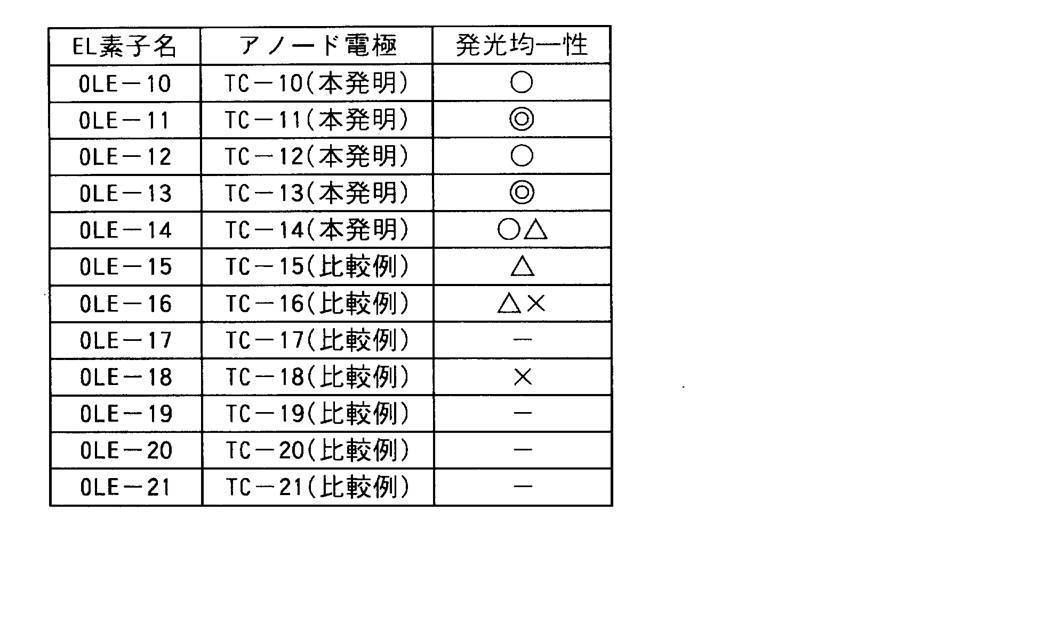
透明電極TC-31の作製(発明例)
透明導電性材料を酸化錫微粒子の分散液に変更し、かつ乾燥後の膜厚が300nmになるよう調整した以外は、実施例1で示したTC-11の製造方法と同様にしてTC-31を作製した。 Example 3
Production of transparent electrode TC-31 (Invention example)
TC-31 is the same as the method for producing TC-11 shown in Example 1, except that the transparent conductive material is changed to a dispersion of tin oxide fine particles and the thickness after drying is adjusted to 300 nm. Was made.
導電性繊維をSWCNT(Unidym社製、HiPcoR単層カーボンナノチューブ)の分散液に変更し、SWCNTの目付け量が10mg/m2となるよう調整した以外は、実施例1で示したTC-11の製造方法と同様にしてTC-41を作製した。 Production of transparent electrode TC-41 (Invention example)
Except for changing the conductive fiber to a dispersion of SWCNT (manufactured by Unidym, HiPcoR single-walled carbon nanotube) and adjusting the basis weight of SWCNT to 10 mg / m 2 , the TC-11 shown in Example 1 was used. TC-41 was produced in the same manner as the production method.
21 透明導電性材料
31 透明導電層
41 透明バインダー
42 透明バインダー層
51 透明基材 DESCRIPTION OF
Claims (5)
- 透明基材上に透明導電層を有する透明電極であって、該透明導電層は、導電性繊維と透明導電性材料とを含み、該透明導電層の表面は、導電性繊維と透明導電性材料とで構成されており、かつ該透明導電層の表面の平滑性が1nm≦Ry≦50nmであることを特徴とする透明電極。
但し、Ryは、最大高さ(表面の山頂部と谷底部との高低差)を意味し、JIS B601(1994)に規定される表面粗さに準ずる値である。 A transparent electrode having a transparent conductive layer on a transparent substrate, wherein the transparent conductive layer includes conductive fibers and a transparent conductive material, and the surface of the transparent conductive layer includes conductive fibers and a transparent conductive material. And the smoothness of the surface of the transparent conductive layer is 1 nm ≦ Ry ≦ 50 nm.
However, Ry means the maximum height (the difference in height between the top and bottom of the surface), and is a value according to the surface roughness defined in JIS B601 (1994). - 前記導電性繊維が、金属ナノワイヤおよびカーボンナノチューブの群から選ばれる少なくとも1種であることを特徴とする請求項1に記載の透明電極。 The transparent electrode according to claim 1, wherein the conductive fiber is at least one selected from the group consisting of metal nanowires and carbon nanotubes.
- 前記透明導電性材料が、導電性高分子および導電性金属酸化物粒子の群から選ばれる少なくとも1種であることを特徴とする請求項1または2に記載の透明電極。 The transparent electrode according to claim 1, wherein the transparent conductive material is at least one selected from the group of conductive polymers and conductive metal oxide particles.
- 前記透明導電層の表面の算術平均粗さRaが0.1nm≦Ra≦5nmであることを特徴とする請求項1~3のいずれか1項に記載の透明電極。
但し、Raは算術平均粗さを意味し、JIS B601(1994)に規定される表面粗さに準ずる値である。 The transparent electrode according to any one of claims 1 to 3, wherein the arithmetic average roughness Ra of the surface of the transparent conductive layer is 0.1 nm ≤ Ra ≤ 5 nm.
However, Ra means arithmetic mean roughness and is a value according to the surface roughness prescribed | regulated to JISB601 (1994). - 請求項1~4のいずれか1項に記載の透明電極を製造する、透明電極の製造方法であって、離型面の平滑性が1nm≦Ry≦50nmの離型性基材の離型面上に、導電性繊維と透明導電性材料を含む透明導電層を形成した後、該透明導電層を透明基材上に転写することにより透明電極を形成することを特徴とする透明電極の製造方法。
但し、Ryは、最大高さ(表面の山頂部と谷底部との高低差)を意味し、JIS B601(1994)に規定される表面粗さに準ずる値である。 The method for producing a transparent electrode according to any one of claims 1 to 4, wherein the release surface of the releasable substrate has a release surface smoothness of 1 nm ≤ Ry ≤ 50 nm. A method for producing a transparent electrode, comprising: forming a transparent conductive layer containing conductive fibers and a transparent conductive material; and forming the transparent electrode by transferring the transparent conductive layer onto a transparent substrate. .
However, Ry means the maximum height (the difference in height between the top and bottom of the surface), and is a value according to the surface roughness defined in JIS B601 (1994).
Priority Applications (2)
| Application Number | Priority Date | Filing Date | Title |
|---|---|---|---|
| JP2010521685A JP5454476B2 (en) | 2008-07-25 | 2009-07-16 | Transparent electrode and method for producing transparent electrode |
| US12/933,665 US8198796B2 (en) | 2008-07-25 | 2009-07-16 | Transparent electrode and production method of same |
Applications Claiming Priority (2)
| Application Number | Priority Date | Filing Date | Title |
|---|---|---|---|
| JP2008192042 | 2008-07-25 | ||
| JP2008-192042 | 2008-07-25 |
Publications (1)
| Publication Number | Publication Date |
|---|---|
| WO2010010838A1 true WO2010010838A1 (en) | 2010-01-28 |
Family
ID=41570303
Family Applications (1)
| Application Number | Title | Priority Date | Filing Date |
|---|---|---|---|
| PCT/JP2009/062874 WO2010010838A1 (en) | 2008-07-25 | 2009-07-16 | Transparent electrode and production method of same |
Country Status (3)
| Country | Link |
|---|---|
| US (1) | US8198796B2 (en) |
| JP (1) | JP5454476B2 (en) |
| WO (1) | WO2010010838A1 (en) |
Cited By (38)
| Publication number | Priority date | Publication date | Assignee | Title |
|---|---|---|---|---|
| JP2011124029A (en) * | 2009-12-09 | 2011-06-23 | Alps Electric Co Ltd | Transparent conductive film and its manufacturing method |
| JP2011154940A (en) * | 2010-01-28 | 2011-08-11 | Konica Minolta Holdings Inc | Transparent pattern electrode, method of manufacturing the electrode, and organic electronic device using the electrode and its manufacturing method |
| WO2011105148A1 (en) * | 2010-02-24 | 2011-09-01 | コニカミノルタホールディングス株式会社 | Transparent conductive film and organic electroluminescent element |
| JP2011171092A (en) * | 2010-02-18 | 2011-09-01 | Konica Minolta Holdings Inc | Manufacturing method of organic electroluminescent element and lighting system |
| JP2011175828A (en) * | 2010-02-24 | 2011-09-08 | Konica Minolta Holdings Inc | Transparent conductive film |
| JP2011198642A (en) * | 2010-03-19 | 2011-10-06 | Panasonic Electric Works Co Ltd | Base material with transparent conductive film, and manufacturing method thereof |
| JP2011216621A (en) * | 2010-03-31 | 2011-10-27 | Nissha Printing Co Ltd | Coil for non-contact charging, film with the coil, molding with the coil, electronic apparatus with the coil, and method of manufacturing the molding with the coil |
| JP2011233289A (en) * | 2010-04-26 | 2011-11-17 | Konica Minolta Holdings Inc | Organic light-emitting element |
| WO2011157946A1 (en) * | 2010-06-16 | 2011-12-22 | Arkema France | Method for preparing carbon-nanotube conductive transparent films |
| WO2012016146A1 (en) | 2010-07-30 | 2012-02-02 | The Board Of Trustees Of The Leland Stanford Junior University | Conductive films |
| JP2012027888A (en) * | 2010-07-26 | 2012-02-09 | Samsung Electro-Mechanics Co Ltd | Transparent conductive film for touch panel and method for manufacturing the same |
| WO2012038591A1 (en) * | 2010-09-23 | 2012-03-29 | Beneq Oy | Thin film photovoltaic module |
| WO2012120949A1 (en) * | 2011-03-10 | 2012-09-13 | パナソニック株式会社 | Transparent conductive film, substrate with transparent conductive film, and organic electroluminescence element using same |
| JP2013077419A (en) * | 2011-09-30 | 2013-04-25 | Mitsubishi Materials Corp | Dispersion liquid for anode of organic electroluminescent element, and method for manufacturing anode of organic electroluminescent element |
| CN103109391A (en) * | 2010-09-24 | 2013-05-15 | 加利福尼亚大学董事会 | Nanowire-polymer composite electrodes |
| JP2013521595A (en) * | 2010-02-27 | 2013-06-10 | イノバ ダイナミックス, インコーポレイテッド | Structure with surface embedding additive and associated manufacturing method |
| JP2013524536A (en) * | 2010-04-06 | 2013-06-17 | メルク パテント ゲーエムベーハー | New electrode |
| JP2013527612A (en) * | 2010-05-21 | 2013-06-27 | メルク パテント ゲゼルシャフト ミット ベシュレンクテル ハフツング | Selective etching of carbon nanotube (CNT) polymer matrix onto plastic substructure |
| JP2013527790A (en) * | 2010-03-04 | 2013-07-04 | ガーディアン・インダストリーズ・コーポレーション | Method for producing coated article comprising alloyed carbon nanotube thin film |
| US20130284242A1 (en) * | 2011-02-01 | 2013-10-31 | University Of South Florida | Partially-sprayed layer organic solar photovoltaic cell using a self-assembled monolayer and method of manufacture |
| JP2013541798A (en) * | 2010-03-04 | 2013-11-14 | ガーディアン・インダストリーズ・コーポレーション | Large area transparent conductive coating comprising doped carbon nanotubes and nanowire composites, and method of manufacturing the same |
| WO2014088186A1 (en) * | 2012-12-07 | 2014-06-12 | 제일모직주식회사 | Composition for transparent electrode and transparent electrode formed from composition |
| KR20140095488A (en) * | 2011-10-13 | 2014-08-01 | 캄브리오스 테크놀로지즈 코포레이션 | Opto-electrical devices incorporating metal nanowires |
| KR20150038013A (en) * | 2012-07-24 | 2015-04-08 | 주식회사 다이셀 | Conductive fiber-coated particle, curable composition and cured article derived from curable composition |
| WO2015056445A1 (en) * | 2013-10-16 | 2015-04-23 | 日立化成株式会社 | Laminate containig conductive fiber, photosensitive conductive film, method for producing conductive pattern, conductive pattern substrate, and touch panel |
| JP2015524883A (en) * | 2013-04-10 | 2015-08-27 | ▲ホア▼▲ウェイ▼技術有限公司 | Graphene fiber and method for forming the same |
| WO2015142077A1 (en) * | 2014-03-19 | 2015-09-24 | 삼성에스디아이 주식회사 | Transparent conductor, method for manufacturing same, and optical display device comprising same |
| US9185798B2 (en) | 2010-08-07 | 2015-11-10 | Innova Dynamics, Inc. | Device components with surface-embedded additives and related manufacturing methods |
| KR101570570B1 (en) | 2012-12-07 | 2015-11-19 | 제일모직주식회사 | Composition for Transparent Electrode and Transparent Electrode Formed with Same |
| US9490454B2 (en) | 2012-07-20 | 2016-11-08 | The Regents Of The University Of California | Method for producing a high efficiency organic light emitting device having a transparent composite electrode comprising a film of conductive nanowires, carbon nanoparticles, light scattering nanoparticles, and a polymer support |
| JP2016196179A (en) * | 2015-04-06 | 2016-11-24 | 大日本印刷株式会社 | Production method of conductive film and conductive film |
| KR20160138165A (en) * | 2014-03-20 | 2016-12-02 | 챔프 그레이트 인터내셔널 코포레이션 | Improved light stability of nanowire-based transparent conductors |
| US10024840B2 (en) | 2007-05-29 | 2018-07-17 | Tpk Holding Co., Ltd. | Surfaces having particles and related methods |
| US10105875B2 (en) | 2008-08-21 | 2018-10-23 | Cam Holding Corporation | Enhanced surfaces, coatings, and related methods |
| KR20210069849A (en) * | 2019-12-04 | 2021-06-14 | 재단법인 한국탄소산업진흥원 | Method for manufacturing high conductive transparent electrode |
| JP6927448B1 (en) * | 2021-04-27 | 2021-09-01 | 東洋インキScホールディングス株式会社 | Thermoplastic resin composition and molded product for electromagnetic wave absorber |
| US11247444B2 (en) | 2015-04-06 | 2022-02-15 | Dai Nippon Printing Co., Ltd. | Electroconductive layered product, touch panel, and process for producing electroconductive layered product |
| CN114235227A (en) * | 2021-12-03 | 2022-03-25 | 明鑫(深圳)技术研究有限公司 | Flexible stress electrode and preparation method thereof |
Families Citing this family (63)
| Publication number | Priority date | Publication date | Assignee | Title |
|---|---|---|---|---|
| US8748799B2 (en) | 2010-12-14 | 2014-06-10 | Zena Technologies, Inc. | Full color single pixel including doublet or quadruplet si nanowires for image sensors |
| US9082673B2 (en) | 2009-10-05 | 2015-07-14 | Zena Technologies, Inc. | Passivated upstanding nanostructures and methods of making the same |
| US8229255B2 (en) | 2008-09-04 | 2012-07-24 | Zena Technologies, Inc. | Optical waveguides in image sensors |
| US9406709B2 (en) | 2010-06-22 | 2016-08-02 | President And Fellows Of Harvard College | Methods for fabricating and using nanowires |
| US8274039B2 (en) | 2008-11-13 | 2012-09-25 | Zena Technologies, Inc. | Vertical waveguides with various functionality on integrated circuits |
| US8866065B2 (en) | 2010-12-13 | 2014-10-21 | Zena Technologies, Inc. | Nanowire arrays comprising fluorescent nanowires |
| US9299866B2 (en) | 2010-12-30 | 2016-03-29 | Zena Technologies, Inc. | Nanowire array based solar energy harvesting device |
| US8519379B2 (en) | 2009-12-08 | 2013-08-27 | Zena Technologies, Inc. | Nanowire structured photodiode with a surrounding epitaxially grown P or N layer |
| US8546742B2 (en) | 2009-06-04 | 2013-10-01 | Zena Technologies, Inc. | Array of nanowires in a single cavity with anti-reflective coating on substrate |
| US20100148221A1 (en) * | 2008-11-13 | 2010-06-17 | Zena Technologies, Inc. | Vertical photogate (vpg) pixel structure with nanowires |
| US8269985B2 (en) | 2009-05-26 | 2012-09-18 | Zena Technologies, Inc. | Determination of optimal diameters for nanowires |
| US8889455B2 (en) | 2009-12-08 | 2014-11-18 | Zena Technologies, Inc. | Manufacturing nanowire photo-detector grown on a back-side illuminated image sensor |
| US8735797B2 (en) | 2009-12-08 | 2014-05-27 | Zena Technologies, Inc. | Nanowire photo-detector grown on a back-side illuminated image sensor |
| US9515218B2 (en) | 2008-09-04 | 2016-12-06 | Zena Technologies, Inc. | Vertical pillar structured photovoltaic devices with mirrors and optical claddings |
| US9478685B2 (en) | 2014-06-23 | 2016-10-25 | Zena Technologies, Inc. | Vertical pillar structured infrared detector and fabrication method for the same |
| US8299472B2 (en) | 2009-12-08 | 2012-10-30 | Young-June Yu | Active pixel sensor with nanowire structured photodetectors |
| US9000353B2 (en) | 2010-06-22 | 2015-04-07 | President And Fellows Of Harvard College | Light absorption and filtering properties of vertically oriented semiconductor nano wires |
| US9343490B2 (en) | 2013-08-09 | 2016-05-17 | Zena Technologies, Inc. | Nanowire structured color filter arrays and fabrication method of the same |
| US8791470B2 (en) | 2009-10-05 | 2014-07-29 | Zena Technologies, Inc. | Nano structured LEDs |
| US8835831B2 (en) | 2010-06-22 | 2014-09-16 | Zena Technologies, Inc. | Polarized light detecting device and fabrication methods of the same |
| US8890271B2 (en) | 2010-06-30 | 2014-11-18 | Zena Technologies, Inc. | Silicon nitride light pipes for image sensors |
| JP5472299B2 (en) * | 2009-06-24 | 2014-04-16 | コニカミノルタ株式会社 | Transparent electrode, method for purifying conductive fiber used for transparent electrode, and organic electroluminescence device |
| JP5363592B2 (en) * | 2010-05-19 | 2013-12-11 | 東海ゴム工業株式会社 | Conductive film, transducer using the same, and flexible wiring board |
| KR20120044654A (en) * | 2010-10-28 | 2012-05-08 | 삼성모바일디스플레이주식회사 | Display device, manufacturing method of the display device, organic light emitting diode display |
| US20120103660A1 (en) * | 2010-11-02 | 2012-05-03 | Cambrios Technologies Corporation | Grid and nanostructure transparent conductor for low sheet resistance applications |
| US20120156458A1 (en) * | 2010-12-16 | 2012-06-21 | Innovation & Infinity Global Corp. | Diffusion barrier structure, transparent conductive structure and method for making the same |
| KR101839954B1 (en) * | 2010-12-17 | 2018-03-20 | 삼성디스플레이 주식회사 | Display device and organic light emitting diode display |
| US9175183B2 (en) * | 2011-05-23 | 2015-11-03 | Carestream Health, Inc. | Transparent conductive films, methods, and articles |
| TWI512555B (en) | 2011-06-09 | 2015-12-11 | Shih Hua Technology Ltd | Touch panel and method for making the same |
| CN102820073A (en) * | 2011-06-09 | 2012-12-12 | 天津富纳源创科技有限公司 | Patterned conducting element |
| TWI447978B (en) | 2011-06-09 | 2014-08-01 | Shih Hua Technology Ltd | Method for making touch panel |
| TWI457808B (en) | 2011-06-09 | 2014-10-21 | Shih Hua Technology Ltd | Touch screen |
| TWI428667B (en) | 2011-06-09 | 2014-03-01 | Shih Hua Technology Ltd | Method for making touch panel |
| TWI528388B (en) | 2011-06-09 | 2016-04-01 | 識驊科技股份有限公司 | Pattern conductive element |
| TWI425562B (en) | 2011-06-09 | 2014-02-01 | Shih Hua Technology Ltd | Method for making touch panel |
| WO2013025491A1 (en) * | 2011-08-12 | 2013-02-21 | Kang James W | Foldable display structures |
| IN2014DN03390A (en) * | 2011-10-03 | 2015-06-05 | Hitachi Chemical Co Ltd | |
| EP2800994A4 (en) * | 2011-10-13 | 2015-10-07 | Univ California | Solution processed nanoparticle-nanowire composite film as a transparent conductor for opto-electronic devices |
| US9202945B2 (en) * | 2011-12-23 | 2015-12-01 | Nokia Technologies Oy | Graphene-based MIM diode and associated methods |
| CN102623606A (en) * | 2012-03-31 | 2012-08-01 | 中国科学院半导体研究所 | Gallium-nitride-based light-emitting diode with silver nanowire transparent electrode and manufacturing method of gallium-nitride-based light-emitting diode |
| US20130323411A1 (en) * | 2012-06-01 | 2013-12-05 | Nuovo Film Inc. | Low Haze Transparent Conductive Electrodes and Method of Making the Same |
| US10029916B2 (en) | 2012-06-22 | 2018-07-24 | C3Nano Inc. | Metal nanowire networks and transparent conductive material |
| US9920207B2 (en) | 2012-06-22 | 2018-03-20 | C3Nano Inc. | Metal nanostructured networks and transparent conductive material |
| US8993998B2 (en) * | 2012-07-02 | 2015-03-31 | The Regents Of The University Of California | Electro-optic device having nanowires interconnected into a network of nanowires |
| FR2996358B1 (en) * | 2012-10-03 | 2016-01-08 | Hutchinson | TRANSPARENT ELECTRODE AND METHOD FOR MANUFACTURING THE SAME |
| KR20140046923A (en) * | 2012-10-11 | 2014-04-21 | 제일모직주식회사 | Transparent conductor, composition for manufacturing the same and optical display apparatus comprising the same |
| TWI552211B (en) * | 2012-11-30 | 2016-10-01 | 恆顥科技股份有限公司 | Touch electrode device |
| US20150325712A1 (en) * | 2012-12-10 | 2015-11-12 | Inna Kozinsky | Nanostructured Thin-Film Solar Cell |
| US10020807B2 (en) | 2013-02-26 | 2018-07-10 | C3Nano Inc. | Fused metal nanostructured networks, fusing solutions with reducing agents and methods for forming metal networks |
| US20140251420A1 (en) * | 2013-03-11 | 2014-09-11 | Tsmc Solar Ltd. | Transparent conductive oxide layer with localized electric field distribution and photovoltaic device thereof |
| WO2014145609A1 (en) | 2013-03-15 | 2014-09-18 | University Of South Florida | Mask-stack-shift method to fabricate organic solar array by spray |
| WO2014150577A1 (en) | 2013-03-15 | 2014-09-25 | Sinovia Technologies | Photoactive transparent conductive films, method of making them and touch sensitive device comprising said films |
| US11274223B2 (en) | 2013-11-22 | 2022-03-15 | C3 Nano, Inc. | Transparent conductive coatings based on metal nanowires and polymer binders, solution processing thereof, and patterning approaches |
| US11343911B1 (en) | 2014-04-11 | 2022-05-24 | C3 Nano, Inc. | Formable transparent conductive films with metal nanowires |
| US9183968B1 (en) | 2014-07-31 | 2015-11-10 | C3Nano Inc. | Metal nanowire inks for the formation of transparent conductive films with fused networks |
| EP3195342A4 (en) * | 2014-08-07 | 2018-04-04 | Flinders Partners Pty Ltd. | Transparent electrode materials and methods for forming same |
| RU2692367C2 (en) | 2014-10-24 | 2019-06-24 | Юнайтед Текнолоджиз Корпорэйшн | Polymer with improved characteristics and method for production thereof |
| CN104464955A (en) * | 2014-11-28 | 2015-03-25 | 中国科学院金属研究所 | Method for manufacturing large-area high-performance graphene composite transparent conductive films on large scale |
| CN104485345A (en) * | 2014-12-15 | 2015-04-01 | 京东方科技集团股份有限公司 | Flexible electrode structure, manufacturing method thereof and flexible display substrate |
| US10309026B2 (en) | 2015-09-01 | 2019-06-04 | International Business Machines Corporation | Stabilization of metallic nanowire meshes via encapsulation |
| DE102015015452A1 (en) * | 2015-12-02 | 2017-06-08 | Forschungszentrum Jülich GmbH | Process for planarizing nanostructures |
| CN112074965A (en) * | 2018-03-16 | 2020-12-11 | 株式会社东芝 | Method and apparatus for manufacturing transparent electrode |
| US20210151701A1 (en) * | 2018-04-12 | 2021-05-20 | The Regents Of The University Of California | HIGHLY EFFICIENT PEROVSKITE/Cu(In, Ga)Se2 TANDEM SOLAR CELL |
Citations (6)
| Publication number | Priority date | Publication date | Assignee | Title |
|---|---|---|---|---|
| WO2008075771A1 (en) * | 2006-12-21 | 2008-06-26 | Fujifilm Corporation | Conductive film and method for manufacturing the same |
| WO2009054273A1 (en) * | 2007-10-26 | 2009-04-30 | Konica Minolta Holdings, Inc. | Transparent conducive film and method for producing the same |
| WO2009060717A1 (en) * | 2007-11-07 | 2009-05-14 | Konica Minolta Holdings, Inc. | Transparent electrode and method for producing transparent electrode |
| WO2009063744A1 (en) * | 2007-11-16 | 2009-05-22 | Konica Minolta Holdings, Inc. | Method for producing metal nanowire, metal nanowire and transparent conductor |
| JP2009205924A (en) * | 2008-02-27 | 2009-09-10 | Kuraray Co Ltd | Transparent conductive film, transparent conductive member, and silver nano wire dispersion solution and manufacturing method of transparent conductive film |
| JP2009231029A (en) * | 2008-03-22 | 2009-10-08 | Konica Minolta Holdings Inc | Method of manufacturing transparent conductive film, and transparent conductive film |
Family Cites Families (10)
| Publication number | Priority date | Publication date | Assignee | Title |
|---|---|---|---|---|
| JP3251066B2 (en) | 1992-08-31 | 2002-01-28 | 富士チタン工業株式会社 | Method for producing acicular conductive fine powder |
| JPH06273964A (en) | 1993-03-18 | 1994-09-30 | Fujitsu Ltd | Photosensitive body, electrophotographic device using it and production of the photosensitive body |
| US6914372B1 (en) * | 1999-10-12 | 2005-07-05 | Matsushita Electric Industrial Co., Ltd. | Electron-emitting element and electron source, field emission image display device, and fluorescent lamp utilizing the same and methods of fabricating the same |
| JP2004220907A (en) * | 2003-01-15 | 2004-08-05 | Dainippon Printing Co Ltd | Organic el display and transparent electrode substrate for display |
| JP2004230690A (en) | 2003-01-30 | 2004-08-19 | Takiron Co Ltd | Antistatic transparent resin sheet |
| JP4606824B2 (en) | 2004-09-14 | 2011-01-05 | 共同印刷株式会社 | Manufacturing method of organic EL display |
| US20070153362A1 (en) | 2004-12-27 | 2007-07-05 | Regents Of The University Of California | Fabric having nanostructured thin-film networks |
| US20060188721A1 (en) * | 2005-02-22 | 2006-08-24 | Eastman Kodak Company | Adhesive transfer method of carbon nanotube layer |
| JP2006310729A (en) * | 2005-03-28 | 2006-11-09 | Dainippon Printing Co Ltd | Organic thin film solar cell |
| EP2251389B8 (en) | 2005-08-12 | 2012-09-19 | Cambrios Technologies Corporation | Nanowire ink |
-
2009
- 2009-07-16 US US12/933,665 patent/US8198796B2/en active Active
- 2009-07-16 JP JP2010521685A patent/JP5454476B2/en active Active
- 2009-07-16 WO PCT/JP2009/062874 patent/WO2010010838A1/en active Application Filing
Patent Citations (6)
| Publication number | Priority date | Publication date | Assignee | Title |
|---|---|---|---|---|
| WO2008075771A1 (en) * | 2006-12-21 | 2008-06-26 | Fujifilm Corporation | Conductive film and method for manufacturing the same |
| WO2009054273A1 (en) * | 2007-10-26 | 2009-04-30 | Konica Minolta Holdings, Inc. | Transparent conducive film and method for producing the same |
| WO2009060717A1 (en) * | 2007-11-07 | 2009-05-14 | Konica Minolta Holdings, Inc. | Transparent electrode and method for producing transparent electrode |
| WO2009063744A1 (en) * | 2007-11-16 | 2009-05-22 | Konica Minolta Holdings, Inc. | Method for producing metal nanowire, metal nanowire and transparent conductor |
| JP2009205924A (en) * | 2008-02-27 | 2009-09-10 | Kuraray Co Ltd | Transparent conductive film, transparent conductive member, and silver nano wire dispersion solution and manufacturing method of transparent conductive film |
| JP2009231029A (en) * | 2008-03-22 | 2009-10-08 | Konica Minolta Holdings Inc | Method of manufacturing transparent conductive film, and transparent conductive film |
Cited By (68)
| Publication number | Priority date | Publication date | Assignee | Title |
|---|---|---|---|---|
| US10024840B2 (en) | 2007-05-29 | 2018-07-17 | Tpk Holding Co., Ltd. | Surfaces having particles and related methods |
| US10105875B2 (en) | 2008-08-21 | 2018-10-23 | Cam Holding Corporation | Enhanced surfaces, coatings, and related methods |
| JP2011124029A (en) * | 2009-12-09 | 2011-06-23 | Alps Electric Co Ltd | Transparent conductive film and its manufacturing method |
| JP2011154940A (en) * | 2010-01-28 | 2011-08-11 | Konica Minolta Holdings Inc | Transparent pattern electrode, method of manufacturing the electrode, and organic electronic device using the electrode and its manufacturing method |
| JP2011171092A (en) * | 2010-02-18 | 2011-09-01 | Konica Minolta Holdings Inc | Manufacturing method of organic electroluminescent element and lighting system |
| WO2011105148A1 (en) * | 2010-02-24 | 2011-09-01 | コニカミノルタホールディングス株式会社 | Transparent conductive film and organic electroluminescent element |
| JP2011175828A (en) * | 2010-02-24 | 2011-09-08 | Konica Minolta Holdings Inc | Transparent conductive film |
| JP5660121B2 (en) * | 2010-02-24 | 2015-01-28 | コニカミノルタ株式会社 | Transparent conductive film and organic electroluminescence element |
| JP2013521595A (en) * | 2010-02-27 | 2013-06-10 | イノバ ダイナミックス, インコーポレイテッド | Structure with surface embedding additive and associated manufacturing method |
| JP2013527790A (en) * | 2010-03-04 | 2013-07-04 | ガーディアン・インダストリーズ・コーポレーション | Method for producing coated article comprising alloyed carbon nanotube thin film |
| JP2013541798A (en) * | 2010-03-04 | 2013-11-14 | ガーディアン・インダストリーズ・コーポレーション | Large area transparent conductive coating comprising doped carbon nanotubes and nanowire composites, and method of manufacturing the same |
| JP2011198642A (en) * | 2010-03-19 | 2011-10-06 | Panasonic Electric Works Co Ltd | Base material with transparent conductive film, and manufacturing method thereof |
| JP2011216621A (en) * | 2010-03-31 | 2011-10-27 | Nissha Printing Co Ltd | Coil for non-contact charging, film with the coil, molding with the coil, electronic apparatus with the coil, and method of manufacturing the molding with the coil |
| JP2013524536A (en) * | 2010-04-06 | 2013-06-17 | メルク パテント ゲーエムベーハー | New electrode |
| JP2016115944A (en) * | 2010-04-06 | 2016-06-23 | メルク パテント ゲーエムベーハー | Novel electrode |
| JP2011233289A (en) * | 2010-04-26 | 2011-11-17 | Konica Minolta Holdings Inc | Organic light-emitting element |
| JP2013527612A (en) * | 2010-05-21 | 2013-06-27 | メルク パテント ゲゼルシャフト ミット ベシュレンクテル ハフツング | Selective etching of carbon nanotube (CNT) polymer matrix onto plastic substructure |
| FR2961625A1 (en) * | 2010-06-16 | 2011-12-23 | Arkema France | PROCESS FOR THE PREPARATION OF CONDUCTIVE TRANSPARENT FILMS BASED ON CARBON NANOTUBES |
| FR2961626A1 (en) * | 2010-06-16 | 2011-12-23 | Arkema France | PROCESS FOR THE PREPARATION OF CONDUCTIVE TRANSPARENT FILMS BASED ON CARBON NANOTUBES. |
| WO2011157946A1 (en) * | 2010-06-16 | 2011-12-22 | Arkema France | Method for preparing carbon-nanotube conductive transparent films |
| JP2012027888A (en) * | 2010-07-26 | 2012-02-09 | Samsung Electro-Mechanics Co Ltd | Transparent conductive film for touch panel and method for manufacturing the same |
| WO2012016146A1 (en) | 2010-07-30 | 2012-02-02 | The Board Of Trustees Of The Leland Stanford Junior University | Conductive films |
| EP2598942A1 (en) * | 2010-07-30 | 2013-06-05 | The Board of Trustees of The Leland Stanford Junior University | Conductive films |
| US9112166B2 (en) | 2010-07-30 | 2015-08-18 | The Board Of Trustees Of The Leland Stanford Junior Univerity | Conductive films |
| EP2598942A4 (en) * | 2010-07-30 | 2014-07-23 | Univ Leland Stanford Junior | Conductive films |
| US9713254B2 (en) | 2010-08-07 | 2017-07-18 | Tpk Holding Co., Ltd | Device components with surface-embedded additives and related manufacturing methods |
| US9185798B2 (en) | 2010-08-07 | 2015-11-10 | Innova Dynamics, Inc. | Device components with surface-embedded additives and related manufacturing methods |
| WO2012038591A1 (en) * | 2010-09-23 | 2012-03-29 | Beneq Oy | Thin film photovoltaic module |
| US9824789B2 (en) | 2010-09-24 | 2017-11-21 | The Regents Of The University Of California | Method for producing nanowire-polymer composite electrodes |
| EP2619816A4 (en) * | 2010-09-24 | 2014-06-11 | Univ California | Nanowire-polymer composite electrodes |
| CN103109391B (en) * | 2010-09-24 | 2016-07-20 | 加利福尼亚大学董事会 | Nanowire-polymer composite electrode |
| EP2619816A2 (en) * | 2010-09-24 | 2013-07-31 | The Regents of the University of California | Nanowire-polymer composite electrodes |
| CN103109391A (en) * | 2010-09-24 | 2013-05-15 | 加利福尼亚大学董事会 | Nanowire-polymer composite electrodes |
| US9401437B2 (en) * | 2011-02-01 | 2016-07-26 | University Of South Florida | Partially-sprayed layer organic solar photovoltaic cell using a self-assembled monolayer and method of manufacture |
| US20130284242A1 (en) * | 2011-02-01 | 2013-10-31 | University Of South Florida | Partially-sprayed layer organic solar photovoltaic cell using a self-assembled monolayer and method of manufacture |
| US20130122279A1 (en) * | 2011-03-10 | 2013-05-16 | Panasonic Corporation | Transparent conductive film, substrate with transparent conductive film, and organic electroluminescence element using the same |
| US9017807B2 (en) * | 2011-03-10 | 2015-04-28 | Panasonic Intellectual Property Management Co., Ltd. | Transparent conductive film, substrate with transparent conductive film, and organic electroluminescence element using the same |
| WO2012120949A1 (en) * | 2011-03-10 | 2012-09-13 | パナソニック株式会社 | Transparent conductive film, substrate with transparent conductive film, and organic electroluminescence element using same |
| JP2012187824A (en) * | 2011-03-10 | 2012-10-04 | Panasonic Corp | Transparent conductive film, substrate with transparent conductive film, and organic electroluminescence element using the same |
| JP2013077419A (en) * | 2011-09-30 | 2013-04-25 | Mitsubishi Materials Corp | Dispersion liquid for anode of organic electroluminescent element, and method for manufacturing anode of organic electroluminescent element |
| JP2014534572A (en) * | 2011-10-13 | 2014-12-18 | カンブリオス テクノロジーズ コーポレイション | Optical / electrical devices with electrodes incorporating nanowires |
| KR20140095488A (en) * | 2011-10-13 | 2014-08-01 | 캄브리오스 테크놀로지즈 코포레이션 | Opto-electrical devices incorporating metal nanowires |
| US10636970B2 (en) | 2011-10-13 | 2020-04-28 | Cambrios Film Solutions Corporation | Opto-electrical devices incorporating metal nanowires |
| KR101999253B1 (en) * | 2011-10-13 | 2019-10-01 | 캄브리오스 필름 솔루션스 코포레이션 | Opto-electrical devices with electrode incorporating metal nanowires |
| US9490454B2 (en) | 2012-07-20 | 2016-11-08 | The Regents Of The University Of California | Method for producing a high efficiency organic light emitting device having a transparent composite electrode comprising a film of conductive nanowires, carbon nanoparticles, light scattering nanoparticles, and a polymer support |
| US10839977B2 (en) | 2012-07-24 | 2020-11-17 | Daicel Corporation | Conductive fiber-coated particle, curable composition and cured article derived from curable composition |
| KR20150038013A (en) * | 2012-07-24 | 2015-04-08 | 주식회사 다이셀 | Conductive fiber-coated particle, curable composition and cured article derived from curable composition |
| KR102032186B1 (en) * | 2012-07-24 | 2019-10-15 | 주식회사 다이셀 | Conductive fiber-coated particle, curable composition and cured article derived from curable composition |
| US9842668B2 (en) | 2012-12-07 | 2017-12-12 | Samsung Sdi Co., Ltd. | Composition for transparent electrode and transparent electrode formed from composition |
| KR101570570B1 (en) | 2012-12-07 | 2015-11-19 | 제일모직주식회사 | Composition for Transparent Electrode and Transparent Electrode Formed with Same |
| WO2014088186A1 (en) * | 2012-12-07 | 2014-06-12 | 제일모직주식회사 | Composition for transparent electrode and transparent electrode formed from composition |
| JP2015524883A (en) * | 2013-04-10 | 2015-08-27 | ▲ホア▼▲ウェイ▼技術有限公司 | Graphene fiber and method for forming the same |
| US10145029B2 (en) | 2013-04-10 | 2018-12-04 | Huawei Technologies Co., Ltd. | Graphene fiber and prepartion method thereof |
| JP5858197B2 (en) * | 2013-10-16 | 2016-02-10 | 日立化成株式会社 | Laminated body including conductive fiber, photosensitive conductive film, method for manufacturing conductive pattern, conductive pattern substrate, and touch panel |
| WO2015056445A1 (en) * | 2013-10-16 | 2015-04-23 | 日立化成株式会社 | Laminate containig conductive fiber, photosensitive conductive film, method for producing conductive pattern, conductive pattern substrate, and touch panel |
| US10795469B2 (en) | 2013-10-16 | 2020-10-06 | Hitachi Chemical Company, Ltd. | Laminate containing conductive fiber, photosensitive conductive film, method for producing conductive pattern, conductive pattern substrate, and touch panel |
| JP2016048688A (en) * | 2013-10-16 | 2016-04-07 | 日立化成株式会社 | Method for inhibiting deterioration of metal fiber, film, and method for producing film |
| WO2015142077A1 (en) * | 2014-03-19 | 2015-09-24 | 삼성에스디아이 주식회사 | Transparent conductor, method for manufacturing same, and optical display device comprising same |
| KR102302408B1 (en) | 2014-03-20 | 2021-09-16 | 캄브리오스 필름 솔루션스 코포레이션 | Improved light stability of nanowire-based transparent conductors |
| KR20160138165A (en) * | 2014-03-20 | 2016-12-02 | 챔프 그레이트 인터내셔널 코포레이션 | Improved light stability of nanowire-based transparent conductors |
| US11247444B2 (en) | 2015-04-06 | 2022-02-15 | Dai Nippon Printing Co., Ltd. | Electroconductive layered product, touch panel, and process for producing electroconductive layered product |
| JP2016196179A (en) * | 2015-04-06 | 2016-11-24 | 大日本印刷株式会社 | Production method of conductive film and conductive film |
| US11760070B2 (en) | 2015-04-06 | 2023-09-19 | Dai Nippon Printing Co., Ltd. | Electroconductive layered product, touch panel, and process for producing electroconductive layered product |
| KR20210069849A (en) * | 2019-12-04 | 2021-06-14 | 재단법인 한국탄소산업진흥원 | Method for manufacturing high conductive transparent electrode |
| KR102337128B1 (en) * | 2019-12-04 | 2021-12-09 | 재단법인 한국탄소산업진흥원 | Method for manufacturing high conductive transparent electrode |
| JP6927448B1 (en) * | 2021-04-27 | 2021-09-01 | 東洋インキScホールディングス株式会社 | Thermoplastic resin composition and molded product for electromagnetic wave absorber |
| JP2022168934A (en) * | 2021-04-27 | 2022-11-09 | 東洋インキScホールディングス株式会社 | Thermoplastic resin composition for electromagnetic wave absorber, and molded body |
| CN114235227A (en) * | 2021-12-03 | 2022-03-25 | 明鑫(深圳)技术研究有限公司 | Flexible stress electrode and preparation method thereof |
Also Published As
| Publication number | Publication date |
|---|---|
| JP5454476B2 (en) | 2014-03-26 |
| JPWO2010010838A1 (en) | 2012-01-05 |
| US20110018424A1 (en) | 2011-01-27 |
| US8198796B2 (en) | 2012-06-12 |
Similar Documents
| Publication | Publication Date | Title |
|---|---|---|
| JP5454476B2 (en) | Transparent electrode and method for producing transparent electrode | |
| JP5584991B2 (en) | Transparent electrode, method for producing transparent electrode, and organic electroluminescence element | |
| JP5625256B2 (en) | Transparent electrode, method for producing transparent electrode, and organic electroluminescence element | |
| JP5212377B2 (en) | Transparent electrode and method for producing transparent electrode | |
| JP5391932B2 (en) | Transparent electrode, method for producing transparent electrode, and organic electroluminescence element | |
| JP5397376B2 (en) | Transparent electrode, organic electroluminescence element, and method for producing transparent electrode | |
| JP5359132B2 (en) | Transparent electrode and organic electroluminescence device having the transparent electrode | |
| US8304984B2 (en) | Organic electroluminescent element | |
| JP5397377B2 (en) | Transparent electrode, organic electroluminescence element, and method for producing transparent electrode | |
| JP5533669B2 (en) | Transparent electrode, method for producing the same, and organic electroluminescence device | |
| JP5682694B2 (en) | Transparent conductive film | |
| JP2011054419A (en) | Transparent electrode, organic electroluminescent element, and organic thin-film solar battery element | |
| JP5499617B2 (en) | Transparent electrode and organic electroluminescence device | |
| JP5660121B2 (en) | Transparent conductive film and organic electroluminescence element | |
| WO2011065213A1 (en) | Dispersion, transparent electrode, and organic electro- luminescent element | |
| JP5599980B2 (en) | Conductive film, method for producing the same, and organic electroluminescence element | |
| JP2011070792A (en) | Method for manufacturing transparent electrode, and transparent electrode | |
| JP5333142B2 (en) | Pattern electrode, organic electroluminescence element, and method of manufacturing pattern electrode |
Legal Events
| Date | Code | Title | Description |
|---|---|---|---|
| 121 | Ep: the epo has been informed by wipo that ep was designated in this application |
Ref document number: 09800352 Country of ref document: EP Kind code of ref document: A1 |
|
| WWE | Wipo information: entry into national phase |
Ref document number: 2010521685 Country of ref document: JP |
|
| WWE | Wipo information: entry into national phase |
Ref document number: 12933665 Country of ref document: US |
|
| NENP | Non-entry into the national phase |
Ref country code: DE |
|
| 122 | Ep: pct application non-entry in european phase |
Ref document number: 09800352 Country of ref document: EP Kind code of ref document: A1 |