WO2008100719A1 - Molded optical articles and methods of making same - Google Patents

Molded optical articles and methods of making same Download PDF

Info

Publication number
WO2008100719A1
WO2008100719A1 PCT/US2008/052742 US2008052742W WO2008100719A1 WO 2008100719 A1 WO2008100719 A1 WO 2008100719A1 US 2008052742 W US2008052742 W US 2008052742W WO 2008100719 A1 WO2008100719 A1 WO 2008100719A1
Authority
WO
WIPO (PCT)
Prior art keywords
optical article
silicon
composition
substrate
photopolymerizable composition
Prior art date
Application number
PCT/US2008/052742
Other languages
French (fr)
Inventor
D. Scott Thompson
Larry D. Boardman
Fedja Kecman
Original Assignee
3M Innovative Properties Company
Priority date (The priority date is an assumption and is not a legal conclusion. Google has not performed a legal analysis and makes no representation as to the accuracy of the date listed.)
Filing date
Publication date
Application filed by 3M Innovative Properties Company filed Critical 3M Innovative Properties Company
Priority to JP2009549661A priority Critical patent/JP2010519573A/en
Priority to EP08714157A priority patent/EP2111645A4/en
Priority to CN2008800048785A priority patent/CN101627477B/en
Publication of WO2008100719A1 publication Critical patent/WO2008100719A1/en

Links

Classifications

    • BPERFORMING OPERATIONS; TRANSPORTING
    • B29WORKING OF PLASTICS; WORKING OF SUBSTANCES IN A PLASTIC STATE IN GENERAL
    • B29DPRODUCING PARTICULAR ARTICLES FROM PLASTICS OR FROM SUBSTANCES IN A PLASTIC STATE
    • B29D11/00Producing optical elements, e.g. lenses or prisms
    • B29D11/0073Optical laminates
    • BPERFORMING OPERATIONS; TRANSPORTING
    • B32LAYERED PRODUCTS
    • B32BLAYERED PRODUCTS, i.e. PRODUCTS BUILT-UP OF STRATA OF FLAT OR NON-FLAT, e.g. CELLULAR OR HONEYCOMB, FORM
    • B32B27/00Layered products comprising a layer of synthetic resin
    • BPERFORMING OPERATIONS; TRANSPORTING
    • B29WORKING OF PLASTICS; WORKING OF SUBSTANCES IN A PLASTIC STATE IN GENERAL
    • B29DPRODUCING PARTICULAR ARTICLES FROM PLASTICS OR FROM SUBSTANCES IN A PLASTIC STATE
    • B29D11/00Producing optical elements, e.g. lenses or prisms
    • GPHYSICS
    • G02OPTICS
    • G02BOPTICAL ELEMENTS, SYSTEMS OR APPARATUS
    • G02B1/00Optical elements characterised by the material of which they are made; Optical coatings for optical elements
    • G02B1/02Optical elements characterised by the material of which they are made; Optical coatings for optical elements made of crystals, e.g. rock-salt, semi-conductors
    • GPHYSICS
    • G02OPTICS
    • G02BOPTICAL ELEMENTS, SYSTEMS OR APPARATUS
    • G02B1/00Optical elements characterised by the material of which they are made; Optical coatings for optical elements
    • G02B1/04Optical elements characterised by the material of which they are made; Optical coatings for optical elements made of organic materials, e.g. plastics
    • G02B1/041Lenses
    • YGENERAL TAGGING OF NEW TECHNOLOGICAL DEVELOPMENTS; GENERAL TAGGING OF CROSS-SECTIONAL TECHNOLOGIES SPANNING OVER SEVERAL SECTIONS OF THE IPC; TECHNICAL SUBJECTS COVERED BY FORMER USPC CROSS-REFERENCE ART COLLECTIONS [XRACs] AND DIGESTS
    • Y10TECHNICAL SUBJECTS COVERED BY FORMER USPC
    • Y10TTECHNICAL SUBJECTS COVERED BY FORMER US CLASSIFICATION
    • Y10T428/00Stock material or miscellaneous articles
    • Y10T428/28Web or sheet containing structurally defined element or component and having an adhesive outermost layer

Definitions

  • the invention relates to optical articles, particularly lenses and waveguides, which are made using a silicon-containing resin.
  • Optical articles can be used in a variety of applications. Examples include lenses and light directing optics for solar concentrators and light emitting devices such as light emitting diodes (LEDs). Other examples include light transmitting and directing optical articles such as waveguides used in edgelit backlight assemblies and optical sensors.
  • LEDs light emitting diodes
  • Other examples include light transmitting and directing optical articles such as waveguides used in edgelit backlight assemblies and optical sensors.
  • an optical article comprising: a photopolymerizable composition disposed on a major surface of a substrate, wherein the photopolymerizable composition comprises: a silicon-containing resin comprising silicon-bonded hydrogen and aliphatic unsaturation, and a platinum catalyst providing from about 0.5 to about 30 parts per million of platinum; and the major surface imparts a positive or negative lens to the photopolymerizable composition.
  • the positive or negative lens is a Fresnel lens.
  • the optical article further comprises a curable adhesive-forming composition disposed on the photopolymerizable composition.
  • a method of making an optical article comprising: providing a photopolymerizable composition disposed on a major surface of a first substrate, wherein the photopolymerizable composition comprises: a silicon-containing resin comprising silicon-bonded hydrogen and aliphatic unsaturation, and a platinum catalyst providing from about 0.5 to about 30 parts per million of platinum; and the major surface imparts a positive or negative lens to the photopolymerizable composition; and photopolymerizing the photopolymerizable composition to form a photopolymerized composition, wherein photopolymerizing comprises applying actinic radiation having a wavelength of 700 nm or less.
  • optical articles formed by the methods disclosed herein are also described.
  • Fig. 1 is a schematic illustration of an exemplary method for making molded optical articles.
  • Figs. 2a and 2b are schematic cross sections of exemplary assemblies of optical articles.
  • Figs. 2c and 3 are schematic cross sections of exemplary optical articles.
  • Figs. 4a, 4b and 5a-5c are schematic cross sections of exemplary molds used to make molded optical articles.
  • Fig. 6 is a schematic illustration of an exemplary method for making molded optical articles.
  • Fig. 7 is a photograph of exemplary and comparative silicone discs.
  • Lenses are typically formed from plastics such as acrylic, polycarbonate, and cycloolefm copolymers. Such injection moldable plastics have refractive indices significantly higher than those of the most photostable silicone materials used for optical applications such as encapsulation in LED devices (the refractive index of polydimethylsiloxane is approximately 1.4). In addition, such resins are not as photostable and thermally stable as photothermally stable silicone materials. For example, when used for encapsulation of LED devices, the device stability must be traded against optical efficiency. Because of this, new silicone materials have been developed to mold silicone lenses to improve the photothermal stability of the lens material, which may improve performance of the devices. These thermally cured silicone resin materials, however, also have undesirable characteristics.
  • Optical quality silicone resins that are based on a condensation cure mechanism suffer from very large material shrinkage and generally release one or more volatile byproducts.
  • Optical quality silicones resins that are based on a metal catalyzed (typically metallic platinum or Pt(O) complexes) thermal hydrosilylation cure mechanism help to limit the cure shrinkage associated with condensation cured silicones, but they also require high temperatures to cure the material, because the silicone resin must be highly inhibited to provide a long enough pot life or working time to use the materials in a high temperature molding process. Because of the inhibitors that must be used with the thermally cured silicones, long cycle times are required to fully cure the materials.
  • the optical articles and methods disclosed herein may provide silicon-containing, including silicone, optical articles that can be made using short mold cycle times.
  • the optical articles and methods include the use of one silicon-containing resin comprising silicon-bonded hydrogen and aliphatic unsaturation, where the resin comprises at least a metal-containing catalyst that is activated by actinic radiation. Additionally, the molding processes may allow for low temperatures to be used to reduce internal stress that is developed in the silicone resins.
  • the optical articles disclosed herein may further be used for producing LED devices where the optical articles provide a desired optical output or emission distribution of light.
  • the optical article may constitute the outer layer of the LED device and may provide surface protection and in certain cases may alleviate dust pick up issues common to current commercial silicone encapsulants. It may be desirable for an inner encapsulant layer to be an organosiloxane-containing gel or soft elastomer.
  • the resin used to make the optical article may be selected to be a hard, tough, and/or mechanically robust organosiloxane-containing material.
  • the optical article can also comprise other silicon- containing, mechanically robust non-organosiloxane materials that exhibit excellent photothermal stability.
  • Organosiloxane materials suitable for molding optical articles in this application have been described in US 7,192,795, and the materials must contain at least one metal catalyst that can be activated by actinic radiation, for example, UV radiation with wavelengths between 250 nm and 500 nm. Additionally, the refractive index of the optical article can be selected to be less than that of the inner encapsulant layer. Finally, methods are described which can be used to make optical articles having a variety of shapes and sizes that can be used in a variety of applications, such as waveguides in sensors, waveguides for backlights, and concentrating optical articles, such as Fresnel lens arrays commonly used for photovoltaic applications.
  • molds having cavities shaped for making hemispherical lenses are shown in the figures described herein. This is in no way is meant to limit the choice of shape or design of the optical articles which can be molded using the processes described herein.
  • Fig. 1 is an illustration showing an exemplary method for making molded optical articles.
  • Mold 100 with cavities 105 comprises a sheet or film based mold, which may be formed by a method such as injection molding, thermoforming, or vacuum forming of a plastic sheet or film.
  • the mold is sometimes referred to as a first substrate.
  • the mold can be made from a variety of materials and may or may not be transparent to actinic radiation, particularly UV radiation, which may be used for initiating reaction in the polymerizable composition, also referred to as lens resin or resin.
  • the choice of mold material and design may determine which embodiments are possible. Suitable mold materials may have glass transition temperatures greater than the temperatures used for the process.
  • mold materials include polymeric materials such as fluoroelastomers, polyolef ⁇ ns, polystyrene, polyesters, polyurethanes, polyethers, polycarbonates, polymethyl methacrylate; and inorganic materials comprising ceramics, quartz, sapphire, metals, and certain glasses. Even organic-inorganic hybrid materials may be used as the mold; exemplary hybrid materials include fluorinated materials described by Choi et al. in Langmuir, Vol. 21, page 9390 (2005).
  • the mold may be transparent such as a transparent ceramic; a transparent mold would be useful in cases where the actinic radiation is applied through the mold.
  • the mold can also be non- transparent such as an opaque ceramic, an opaque plastic, or a metal.
  • the mold can be fabricated by conventional machining, diamond turning, contact lithography, projection lithography, interference lithography, etching, or any other suitable technique.
  • the mold may be an original master mold or a daughter mold thereof. Molding may be referred to as reactive embossing.
  • Transparent mold materials include, but are not limited to, fluorinated film molds such as those fabricated from thin Teflon, tetrafluoroethylene hexafluoropropylene vinylidene difluoride terpolymer (THV) from 3M Company and non-fluorinated materials such as polycarbonate, polyethylene terephthalate (PET), polypropylene, and the like.
  • Non-transparent mold materials include thin metal sheet and opaque and/or colored plastics. These plastic molds can be made of thin sheet-like materials with formed cavities; such as can be produced in a thermoforming or vacuum molding process. Molds can also be made by precision machining processes, by cast and cure processes using a master tool or mold, or extrusion replication processes.
  • uncured silicon-containing lens resin 110 To mold 100 with cavities 105 is added uncured silicon-containing lens resin 110. Ideally the lens resin material is filled into the cavity until it is flush with the surface of the mold. If the lens resin is not filled high enough in the cavity, it may be difficult to contact the partially cured lenses 115 and cured lenses 120 to substrate 125. This is particularly problematic when the substrate is a rigid material such a glass.
  • the lens resin once in the mold is irradiated with actinic radiation to produce an at least partially cured lens resin 115. To the mold with the partially cured lens resin 115 is applied substrate 125.
  • the substrate may be PET, polycarbonate, polyethylene, a premask material such as coextruded polyethylene polyvinylacetate films, which cling to flat surfaces and provide a protective function and can be a carrier for the lenses, glass, or any other substrate of interest to give the assembly 130.
  • the substrate may also be transparent.
  • the substrate comprises a pressure sensitive adhesive (PSA) as described below for FIGS. 2a-2c.
  • PSA pressure sensitive adhesive
  • the partially cured lens resin 115 can be converted to give cured lens resin 120 with the application of heat or by storage at room temperature. Applying the substrate 125 to the partially cured lens resin material 115 may allow for the lens resin to build better adhesion to the substrate. Partially curing the lens resin with actinic radiation followed by the application of heat may be the preferred method for rapidly producing cured lens resin 120, when only low intensity light sources are available and rapid manufacturing is required.
  • the uncured lens resin 110 can also be converted to cured lens resin 120 directly using either high intensity UV radiation or a simultaneous combination of radiation and heat. If converted directly to cured lens resin 120, the substrate applied to the cured lens resin 120 in the mold must have an affinity for either the mold 100, the cured lens resin 120, or both to make assembly 135.
  • the mold 100 can optionally be removed from the mold assembly 135 to give another assembly 140 comprising an array of lenses on the substrate.
  • the mold 100 may also be removed before the lens resin is fully cured, provided it is not tacky and is mechanically robust enough to not be damaged as the mold is removed. In most cases it will be preferable to leave the mold in place until the lens resin is fully cured.
  • the lenses on substrate 125, shown in assembly 140, can be removed and used individually if not aggressively adhered to the substrate or if the substrate has release characteristics.
  • substrate 200 comprises PSA
  • the PSA is in contact with the lens resin.
  • the support may comprise a release liner which can be removed to give an assembly 215, as shown in Fig. 2b, which comprises an array of optical articles disposed on a layer of the PSA.
  • a lens with PSA 220 can be made by kiss cutting or die cutting around a lens with PSA from assembly 215.
  • assembly 215 can be applied to another substrate before or after the mold is removed from the assembly.
  • the method described above may further comprise: forming a curable adhesive- forming composition disposed on the photopolymerizable composition; photopolymerizing the photopolymerizable composition to form a photopolymerized composition, wherein photopolymerizing comprises applying actinic radiation having a wavelength of 700 nm or less; and polymerizing the curable adhesive-forming composition to form a pressure sensitive adhesive.
  • Suitable PSAs include (meth)acrylate-based PSAs formed from free-radically polymerizable monomers selected from the group of (meth)acrylates, vinyl monomers, and mixtures thereof.
  • (meth)acrylate refers to both acrylates and methacrylates.
  • Examples of (meth)acrylates include alkyl esters of (meth)acrylic acid wherein the alkyl group has from 1 to 20 carbon atoms, for example, ethyl acrylate, isobornyl methacrylate, and lauryl methacrylate; aromatic esters of (meth)acrylic acid such as benzyl methacrylate; and hydroxyalkyl esters of (meth)acrylic acid such as hydroxy ethyl acrylate.
  • Examples of vinyl monomers include vinyl esters such as vinyl acetate, styrene and derivatives thereof, vinyl halides, vinyl propionates, and mixtures thereof.
  • the substrate is a PSA formed from a (meth)acrylate block copolymer as described in US 7,255,920 B2 (Everaerts et al.). In general, these
  • (meth)acrylate block copolymers comprise: at least two A block polymeric units that are the reaction product of a first monomer composition comprising an alkyl methacrylate, an aralkyl methacrylate, an aryl methacrylate, or a combination thereof, each A block having a Tg of at least 5O 0 C, the methacrylate block copolymer comprising from 20 to 50 weight percent A block; and at least one B block polymeric unit that is the reaction product of a second monomer composition comprising an alkyl (meth)acrylate, a heteroalkyl (meth)acrylate, a vinyl ester, or a combination thereof, the B block having a Tg no greater than 2O 0 C, the (meth)acrylate block copolymer comprising from 50 to 80 weight percent B block; wherein the A block polymeric units are present as nanodomains having an average size less than about 150 nm in a matrix of the B block polymeric units.
  • the substrate is a silicone -based PSA.
  • silicone-based PSAs are those that comprise a high molecular weight silicone gum and a silicate MQ resin, the MQ resin usually present at a level of 50-60 % by weight with respect to solids.
  • Other examples of silicone-based PSAs are described in US 5,169,727 (Boardman).
  • these PSAs are photocurable and are formed from a composition
  • a composition comprising a flowable mixture of (a) a benzene soluble, resinous copolymer having triorganosiloxy and Si ⁇ 4/2 units, (b) a diorganoalkenylsiloxy endblocked polydiorganosiloxane, (c) a diorganohydrogensiloxy endblocked polydiorganosiloxane, (d) an organosilicon crosslinking agent being selected from organosilicon compounds having from 1 to 15 silicon atoms, and (e) a hydrosilation catalyst in an amount sufficient to effect curing of the composition.
  • the silicone-based PSA may also comprise hydrosilylation inhibitors, photosensitizers, fillers, etc.
  • the proper choice of PSA may be determined by the application in which the optical article is to be used.
  • the PSA should be chosen such that it strongly adheres the optical article to the substrate to which it is applied, for example, a hemispherical lens bonded to the surface of the encapsulant of a surface mount light emitting diode package or a Fresnel lens to a glass plate.
  • the PSA does not lose adhesion over time and is stable under the conditions of use. Ideal PSAs do not detract from the optical function of the optical article due to degradation of adhesion or degradation of the PSA material itself due to a lack of photo- and/or thermal stability.
  • Mold 100 may be designed to create a layer of lenses, i.e., lenses with a flat film of cured resin of controlled thickness in the flat areas between lenses. Such a layer of lenses is shown in Fig. 3.
  • This layer of lenses may comprise lenses small enough for use with light emitting diodes.
  • This layer of lenses may be much larger having larger lenses, for example, the layer of lenses may comprise a layer of Fresnel lenses such that the layer can be used as a solar concentrator for photovoltaic cells.
  • the fast, low temperature curing enabled by the photocurable silicon-containing materials may be important to faithfully reproduce the features of the mold and improve manufacturing efficiency.
  • a rigid substrate such a glass plate, may be used as a substrate to which the layer of lenses is attached in order to provide dimensional stability.
  • a flexible substrate may be preferred.
  • Fig. 4a shows an exemplary mold that may be used in the method disclosed herein.
  • Mold 400 comprises first cavity 405.
  • the mold may be a solid block of material and may or may not be transparent to the actinic radiation necessary to initiate reaction in the silicon-containing lens resin. Suitable mold materials may have glass transition temperatures greater than the temperatures used for the process. Such mold materials are described above.
  • Transparent mold materials include, but are not limited to, acrylic, polycarbonate, polypropylene, and other transparent polymeric materials.
  • Non-transparent mold materials include steel, other metals (preferably ones capable of taking a high quality polish), ceramics, and opaque and/or colored plastics.
  • Fig. 4b shows exemplary mold assembly 410 that may be used. Mold assembly 410 comprises second cavity 415 which is formed by mold 400 and substrate 420.
  • either or both of the mold and substrate are transparent to the actinic radiation, particularly UV radiation, which is used for initiating reaction in the uncured lens resin.
  • Uncured silicon-containing lens resin may be added to cavities 405 of mold 400.
  • Substrate 420 can then be applied to form the second cavity which in this case is filled or partially filled with resin.
  • the substrate may comprise acrylic, polycarbonate, polyethylene, glass, etc.
  • the lens resin in the mold is then irradiated with actinic radiation through either or both of the mold and substrate, depending on whether the mold and/or substrate are transparent, to produce an at least partially cured lens resin.
  • the uncured lens resin in the assembly can be converted to cured lens resin with the application of heat or by storage at room temperature.
  • the uncured lens resin can be converted to a fully cured lens resin directly using either high intensity UV irradiation or a simultaneous combination of low intensity radiation and heat.
  • Mold 400 may optionally be removed from the assembly to give an array of lenses on a substrate. If partially cured lens resin in mold assembly is cured to a point of being tack free on the surfaces of the lenses, which are in contact with the mold, the mold can be removed prior to the heating step. Heating of the assembly produces an array of cured lenses on a substrate.
  • This process can be used in a compression molding type process where the mold features are slightly over filled and the substrate, if rigid and strong, can be contacted to the mold with high pressure to force the lens resin into the mold, the excess resin being squeezed out of the mold cavities.
  • thin plastic sheet inserts that are fitted to the molds can be used in the mold assemblies to make the various mold assemblies. Such mold inserts with improved release properties can be used with molds where the optical articles prove difficult to remove from the mold material.
  • Another embodiment of the method disclosed herein comprises transfer molding or low pressure liquid injection molding processes. In order to perform these types of molding processes the mold materials are solid blocks of material and at least part of the mold assembly must be transparent to the actinic radiation necessary to initiate reaction in the silicon-containing lens resin.
  • Suitable mold materials will have glass transition temperatures greater than the temperatures used for the process. Such mold materials are described in above.
  • Transparent mold materials include, but are not limited to, acrylic, polycarbonate, glass and other transparent polymeric materials.
  • the traditional mold material for these types of processes is polished steel.
  • the mold halves are assembled prior to filling the mold with the photocurable silicon-containing resin.
  • the molds In order to fill the mold cavities, the molds must have a system of channels, known as a sprue and runner system.
  • the silicon- containing resin runs through the channels and into the mold cavities typically under pressure.
  • the resin In order to cure the resin at least one of the halves must be transparent to the actinic radiation necessary to initiate reaction in the silicon-containing resin. This is most often UV radiation with wavelengths between 250 nm and 450 nm. To achieve fast mold cycle times the resin may be exposed through the transparent mold to high intensity radiation with optional heating or be exposed to low intensity radiation with the mold heated to elevated temperatures. Once the resin is cured, the mold is opened to give hemispherical lenses.
  • Figs. 5a and 5b illustrate embodiments where the both sides of the mold have structure to create other shapes.
  • Fig. 5a shows two mold halves, each having cavities, which are assembled to form a single cavity.
  • Such design for example, can be used for making optical articles such as aspheric lenses.
  • Fig. 5b shows one side of the mold having a cavity and the other mold half having a protrusion. This type of mold design is used for making structures such as hollow lenses.
  • Fig. 5c illustrates a different type of optical article that can be made.
  • the optical article can be used as waveguide to transmit infrared light in a sensor device from an IR LED to a photodiode detector.
  • the optical articles shown in the figures are illustrative and are not meant to limit the types of, shapes of, and size of optical articles that can be made using the molding processes described herein.
  • the mold processes can be used to produce optical articles that range in size and can have micron size features, macroscopic features and combinations thereof.
  • Fig. 6 illustrates an additional process flow diagram for the case where the mold may or may not be transparent to the actinic radiation needed to cure the lens resin material.
  • This process describes a method to produce molded lenses with a PSA in a single step using a photocured PSA resin.
  • photocurable silicone PSA resins include those described in US 5,169,727 (Boardman et al.) as previously described.
  • a mold 600 with cavities 605 is first added uncured silicon-containing lens resin 610 followed by uncured PSA resin 615.
  • the lens resin and PSA resin in the mold are irradiated with actinic radiation to produce an at least partially cured lens resin 620 and PSA 625.
  • the uncured lens resin can be converted to give a fully cured lens resin material 630 with the application of heat or by storage at room temperature.
  • Substrate 635 can be applied after the PSA is cured to give assemblies 640 and 645.
  • the mold can then be removed to give an assembly 650 comprising an array of lenses with PSA on a substrate.
  • Other molds as described herein may also be used.
  • the mold may be shaped so as to impart any useful structure on the surface of the optical article.
  • the mold may be shaped so as to form a refractive lens.
  • Lensing refers to the uniform (or nearly uniform) curvature of a substantial portion of the surface of the article to form a positive or negative lens.
  • the diameter of the lens may be, for example, approximately the size of a package or reflector cup used to make a light emitting diode (LED) device.
  • a lensed surface can be characterized by a "radius of curvature.”
  • the radius of curvature can be either positive denoting a convex surface, or negative denoting a concave surface, or infinite denoting a flat surface.
  • Lensing can improve light extraction of LED devices by reducing the total internal reflections of light incident at the encapsulant-air interface. It can also change the angular distribution of light emitted from the LED device.
  • a surface of the optical article may also be shaped with macrostructures having a characteristic dimension that is smaller than an LED device package size, but much larger than the wavelength of visible light. That is, each macrostructure may have a dimension of from 10 ⁇ m to 1 mm. The spacing or period between each macrostructure may also be from 10 ⁇ m to 1 mm (or about 1/3 the size of the LED package). Examples of macrostructures include surfaces that, when viewed in cross-section, appear to be shaped like a sine wave, triangular wave, square wave, rectified sine wave, saw tooth wave, cycloid (more generally curtate cycloid), or rippled.
  • the periodicity of the macrostructures may be one- or two-dimensional. Surfaces with one-dimensional periodicity have repeat structures along only one major direction of the surface.
  • the mold may comprise any of the VikuitiTM Brightness Enhancement Films available from 3M Company.
  • the mold may be shaped to impart a lens structure capable of generating a side- emission pattern for an LED device.
  • the optical article may have a central axis, and light entering it is reflected and refracted and eventually exits in a direction substantially perpendicular to the central axis; examples of these types of side emitting lens shapes and devices are described in U.S. 6,679,621 B2 and U.S. 6,598,998 B2.
  • the optical article has a generally planar surface, with a smoothly curved surface defining a vortex shape that extends into the article and has the shape of an equiangular spiral that forms into a cusp; an example of such a profile is described in U.S. 6,473,554 Bl, particularly Figs. 15, 16 and 16A.
  • Surfaces with two-dimensional periodicity have repeat structures along any two orthogonal directions in the plane of the macrostructures.
  • macrostructures with two-dimensional periodicity include random surfaces, two-dimensional sinusoids, arrays of cones, arrays of prisms such as cube-corners, and lenslet arrays.
  • Fig. 4 of US 2006/0092636 shows an elevated view of another exemplary surface shaped as a Fresnal lens having generally circular symmetry and that can be designed to replicate the optical properties of any positive or negative lens while occupying much less volume than a solid lens. Larger Fresnel lenses used for solar concentration in photovoltaic applications may have larger sturctured features, where the structures have sizes in the range of 0.1 mm up to approximately 5 mm or larger.
  • the macrostructures do not need to be uniform in size across the surface. For example, they may get larger or smaller toward the edges of the package, or they may change shape.
  • the surface may consist of any linear combination of shapes described herein.
  • the surface may also be shaped with microstructures having a characteristic dimension on a scale similar to the wavelengths of visible light. That is, each microstructure may have a dimension of from 100 nm to less than 10 ⁇ m. Light tends to diffract when it interacts with microstructured surfaces. Thus, the design of microstructured surfaces requires careful attention to the wave-like nature of light.
  • microstructures are one- and two-dimensional diffraction gratings; one-, two- , or three-dimensional photonic crystals; binary optical articles; and "motheye" anti- reflection coatings.
  • Other examples of microstructures are shown in Figs. 5-7 of US 2006/0092636 (Thompson et al.) and include linear prisms having one-dimensional periodicity, an array of two-dimensional prisms, and a surface molded with microlenses.
  • the microstructures do not need to be uniform in size across the surface.
  • the articles may get larger or smaller toward the edges of the package, or they may change shape.
  • the surface may consist of any linear combination of shapes described herein.
  • Fig. 8 of US 2006/0092636 shows an elevated view of another exemplary surface comprising randomly disposed protrusions and depressions.
  • the surface of the optical article may comprise structures from all three size scales. All package surfaces will be lensed with some radius of curvature, which could be positive, negative, or infinite. A macrostructure or microstructure could be added to the lensed surface to further enhance light output or to optimize the angular distribution for a given application. A surface could even incorporate a microstructure on a macrostructure on a lensed surface.
  • the photopolymerizable compositions utilized in the methods described herein include a silicon-containing resin comprising silicon-bonded hydrogen and aliphatic unsaturation.
  • the silicon-containing resin can include monomers, oligomers, polymers, or mixtures thereof.
  • silicon-bonded hydrogen and aliphatic unsaturation which allows for hydrosilylation (i.e., the addition of a silicon-bonded hydrogen across a carbon- carbon double bond or triple bond).
  • the silicon-bonded hydrogen and the aliphatic unsaturation may or may not be present in the same molecule. Furthermore, the aliphatic unsaturation may or may not be directly bonded to silicon.
  • Preferred silicon-containing resins are those that provide an optical article, which can be in the form of an elastomer or a non-elastic solid, and are thermally and photochemically stable.
  • silicon-containing resins having refractive indices of at least 1.34 are preferred.
  • silicon-containing resins having refractive indices of at least 1.50 are preferred.
  • Preferred silicon-containing resins are selected such that they provide an optical article that is photostable and thermally stable.
  • photostable refers to a material that does not chemically degrade upon prolonged exposure to actinic radiation, particularly with respect to the formation of colored or light absorbing degradation products.
  • thermally stable refers to a material that does not chemically degrade upon prolonged exposure to heat, particularly with respect to the formation of colored or light absorbing degradation products.
  • preferred silicon-containing resins are those that possess relatively rapid cure mechanisms (e.g., seconds to less than 30 minutes) in order to accelerate manufacturing times and reduce overall manufacturing cost. Examples of suitable silicon-containing resins are disclosed, for example, in U.S.
  • a preferred silicon-containing resin comprises an organosiloxane (i.e., silicones), which includes organopolysiloxanes.
  • organosiloxane i.e., silicones
  • Such resins typically include at least two components, one having silicon-bonded hydrogen and one having aliphatic unsaturation. However, both silicon-bonded hydrogen and olefmic unsaturation may exist within the same molecule.
  • the silicon-containing resin can include a silicone component having at least two sites of aliphatic unsaturation (e.g., alkenyl or alkynyl groups) bonded to silicon atoms in a molecule and an organohydrogensilane and/or organohydrogenpolysiloxane component having at least two hydrogen atoms bonded to silicon atoms in a molecule.
  • a silicon-containing resin includes both components, with the silicone containing aliphatic unsaturation as the base polymer (i.e., the major organosiloxane component in the composition.)
  • Preferred silicon-containing resins are organopolysiloxanes.
  • Such resins typically comprise at least two components, at least one of which contains aliphatic unsaturation and at least one of which contains silicon-bonded hydrogen.
  • organopolysiloxanes are known in the art and are disclosed in such patents as US 3,159,662 (Ashby), US 3,220,972 (Lamoreauz), US 3,410,886 (Joy), US 4,609,574 (Keryk), US 5,145,886 (Oxman, et. al), and US 4,916,169 (Boardman et. al). Curable one component organopolysiloxane resins are possible if the single resin component contains both aliphatic unsaturation and silicon-bonded hydrogen.
  • Organopolysiloxanes that contain aliphatic unsaturation are preferably linear, cyclic, or branched organopolysiloxanes comprising units of the formula R 1 a R 2 bSi0(4_ a _b)/2 wherein: R 1 is a monovalent, straight-chained, branched or cyclic, unsubstituted or substituted hydrocarbon group that is free of aliphatic unsaturation and has from 1 to 18 carbon atoms; R 2 is a monovalent hydrocarbon group having aliphatic unsaturation and from 2 to 10 carbon atoms; a is 0, 1, 2, or 3; b is 0, 1, 2, or 3; and the sum a+b is 0, 1, 2, or 3; with the proviso that there is on average at least 1 R 2 present per molecule.
  • Organopolysiloxanes that contain aliphatic unsaturation preferably have an average viscosity of at least 5 mPa-s at 25°C.
  • suitable R 1 groups are alkyl groups such as methyl, ethyl, n-propyl, iso-propyl, n-butyl, iso-butyl, tert-butyl, n-pentyl, iso-pentyl, neo-pentyl, tert-pentyl, cyclopentyl, n-hexyl, cyclohexyl, n-octyl, 2,2,4-trimethylpentyl, n-decyl, n-dodecyl, and n-octadecyl; aromatic groups such as phenyl or naphthyl; alkaryl groups such as 4-tolyl; aralkyl groups such as benzyl, 1-phenylethy
  • R 2 groups examples include alkenyl groups such as vinyl, 5-hexenyl, 1- propenyl, allyl, 3-butenyl, 4-pentenyl, 7-octenyl, and 9-decenyl; and alkynyl groups such as ethynyl, propargyl and 1-propynyl.
  • groups having aliphatic carbon-carbon multiple bonds include groups having cycloaliphatic carbon-carbon multiple bonds.
  • Organopolysiloxanes that contain silicon-bonded hydrogen are preferably linear, cyclic or branched organopolysiloxanes comprising units of the formula R 1 a H c Si0(4_ a _ c y2 wherein: R 1 is as defined above; a is 0, 1, 2, or 3; c is 0, 1, or 2; and the sum of a+c is 0, 1, 2, or 3; with the proviso that there is on average at least 1 silicon-bonded hydrogen atom present per molecule.
  • Organopolysiloxanes that contain silicon-bonded hydrogen preferably have an average viscosity of at least 5 mPa-s at 25°C.
  • Organopolysiloxanes that contain both aliphatic unsaturation and silicon-bonded hydrogen preferably comprise units of both formulae R 1 a R 2 bSi0(4_ a _b)/2 and R 1 a H c SiO(4_ a _ c )/2.
  • R 1 , R 2 , a, b, and c are as defined above, with the proviso that there is an average of at least 1 group containing aliphatic unsaturation and 1 silicon-bonded hydrogen atom per molecule.
  • the molar ratio of silicon-bonded hydrogen atoms to aliphatic unsaturation in the silicon-containing resin may range from 0.5 to 10.0 mol/mol, preferably from 0.8 to 4.0 mol/mol, and more preferably from 1.0 to 3.0 mol/mol.
  • organopolysiloxane resins described above wherein a significant fraction of the R 1 groups are phenyl or other aryl, aralkyl, or alkaryl are preferred, because the incorporation of these groups provides materials having higher refractive indices than materials wherein all of the R 1 radicals are, for example, methyl.
  • compositions also include a metal-containing catalyst which enables the cure of the encapulating material via radiation-activated hydrosilylation.
  • metal-containing catalyst which enables the cure of the encapulating material via radiation-activated hydrosilylation.
  • These catalysts are known in the art and typically include complexes of precious metals such as platinum, rhodium, iridium, cobalt, nickel, and palladium.
  • the precious metal-containing catalyst preferably contains platinum.
  • Disclosed compositions can also include a cocatalyst, i.e., the use of two or more metal-containing catalysts.
  • Certain preferred platinum-containing catalysts are selected from the group consisting of Pt(II) ⁇ -diketonate complexes (such as those disclosed in U.S. Pat. No. 5,145,886 (Oxman et al.), ( ⁇ 5 -cyclopentadienyl)tri( ⁇ -aliphatic)platinum complexes (such as those disclosed in U.S. Pat. No. 4,916,169 (Boardman et al.) and U.S. Pat. No. 4,510,094 (Drahnak)), and C7_2o-aromatic substituted ( ⁇ 5 -cyclopentadienyl)tri( ⁇ - aliphatic)platinum complexes (such as those disclosed in U.S. Pat. No. 6,150,546 (Butts).
  • the amount of catalyst used is discussed below.
  • the photopolymerizable composition can also include nonabsorbing metal oxide particles, semiconductor particles, phosphors, sensitizers, photoinitiators, antioxidants, catalyst inhibitors, and pigments. If used, such additives are used in amounts to produced the desired effect. These additives are further described in US 7,192,795 Bl (Boardman et al.)
  • the disclosed method involves the use of actinic radiation having a wavelength of less than or equal to 700 nanometers (nm).
  • the disclosed methods are particularly advantageous to the extent they avoid harmful temperatures.
  • the disclosed methods involve the application of actinic radiation at a temperature of less than 120 0 C, more preferably, at a temperature of less than 6O 0 C, and still more preferably at a temperature of 25 0 C or less.
  • Actinic radiation used in the disclosed methods includes light of a wide range of wavelengths less than or equal to 700 nm, including visible and UV light, but preferably, the actinic radiation has a wavelength of of 600 nm or less, and more preferably from 200 to 600 nm., and even more preferably, from 250 to 500 nm. Preferably, the actinic radiation has a wavelength of at least 200 nm, and more preferably at least 250 nm.
  • sources of actinic radiation include tungsten halogen lamps, xenon arc lamps, mercury arc lamps, incandescent lamps, germicidal lamps, and fluorescent lamps.
  • the amount of metal-containing catalyst used in a given photopolymerizable composition is said to depend on a variety of factors such as the radiation source, whether or not heat is used, amount of time, temperature, etc., as well as on the particular chemistry of the silicon-containing resin(s), its reactivity, the amount present in the photopolymerizable composition, etc.
  • the metal-containing catalyst may be used in an amount of at least 1 part per million (ppm) of the photopolymerizable composition. Further, it is said that the catalysts are included in amounts of no greater than 1000 parts of metal per one million parts of the photopolymerizable composition.
  • Fig. 7 is a photograph showing side-by-side comparision of two discs made from photopolymerizable compositions comprising silicon-containing resins. Hydrosilylation of components was carried out in the presence of 10 and 50 ppm, respectively, of a platinum catalyst. Details of the experimental procedures can be found in Example 1 and Comparative Example 1 for 10 and 50 ppm, respectively.
  • the photopolymerizable composition comprises a platinum catalyst providing from 0.5 to 30 ppm platinum per one million parts of the photopolymerizable composition.
  • the photopolymerizable composition comprises a platinum catalyst providing 0.5 to 20 ppm platinum per one million parts of the photopolymerizable composition.
  • the photopolymerizable composition comprises a platinum catalyst providing 0.5 to 12 ppm platinum per one million parts of the photopolymerizable composition.
  • the photopolymerizable composition is free of catalyst inhibitor.
  • Minimization of the amounts of materials that can act as catalyst inhibitors can be desirable to maximize the cure speed of the photopolymerizable composition in that active hydrosilylation catalyst generated upon irradiation of the composition is produced in the absence of materials that can attenuate the activity of said active catalyst.
  • a stock catalyst solution was prepared by dissolving 33 mg of MeCpPtMe 3 (Alfa Aesar, Ward Hill, MA) in 1 mL of toluene.
  • Silicone compositions having different amounts of the platinum catalyst were prepared by combining master batch and catalyst solution as follows. All compositions were prepared under safe conditions where light below a wavelength of 500 nm was excluded.
  • the material cures to a tack-free solid in 1 to 2 minutes.
  • the cured silicone disc was removed from the plastic Petri dish and was 2.7 mm in thickness at the center of the silicone disc.
  • a transmission spectrum of the silicone was taken using a PerkinElmer Lambda 900 UV7VIS Spectrophotometer (PerkinElmer Instruments, Norwalk, CT). The transmission of the sample at 400 nm, not corrected for Fresnel reflections, was 93.8%.
  • the sample was placed into a glass Petri dish to protect the surface from contamination by dust and debris and the sample was aged at 130 0 C in a forced air oven for 1000 hours. Transmission data for the sample at 400 nm measured during the 1000 hour aging experiment are shown in Table 1.
  • Transmission data for the sample at 460 nm measured during the 1000 hour aging experiment are shown in Table 3.
  • Transmission data for the sample at 530 nm measured during the 1000 hour aging experiment are shown in Table 5.
  • Transmission data for the sample at 670 nm measured during the 1000 hour aging experiment are shown in Table 7.
  • the cured silicone disc was removed from the plastic Petri dish and was 2.7 mm in thickness at the center of the silicone disc.
  • a transmission spectrum of the silicone was taken using a PerkinElmer Lambda 900 UV7VIS Spectrophotometer (PerkinElmer Instruments, Norwalk, CT). The transmission of the sample at 400 nm, not corrected for Fresnel reflections, was 93.2%.
  • Transmission data for the sample at 400 nm measured during the 1000 hour aging experiment are shown in Table 1.
  • Transmission data for the sample at 460 nm measured during the 1000 hour aging experiment are shown in Table 3.
  • Transmission data for the sample at 530 nm measured during the 1000 hour aging experiment are shown in Table 5.
  • Transmission data for the sample at 670 nm measured during the 1000 hour aging experiment are shown in Table 7.
  • the cured silicone disc was removed from the plastic Petri dish and was 2.7 mm in thickness at the center of the silicone disc.
  • a transmission spectrum of the silicone was taken using a PerkinElmer Lambda 900 UV7VIS Spectrophotometer (PerkinElmer Instruments, Norwalk, CT). The transmission of the sample at 400 nm, not corrected for Fresnel reflections, was 92.6%.
  • Transmission data for the sample at 400 nm measured during the 1000 hour aging experiment are shown in Table 1.
  • Transmission data for the sample at 460 nm measured during the 1000 hour aging experiment are shown in Table 3.
  • Transmission data for the sample at 530 nm measured during the 1000 hour aging experiment are shown in Table 5.
  • Transmission data for the sample at 670 nm measured during the 1000 hour aging experiment are shown in Table 7.
  • the material cures to a tack-free solid in about 1 minute.
  • the cured silicone disc was removed from the plastic Petri dish and was 2.7 mm in thickness at the center of the silicone disc.
  • a transmission spectrum of the silicone was taken using a PerkinElmer Lambda 900 UV7VIS Spectrophotometer (PerkinElmer Instruments, Norwalk, CT). The transmission of the sample at 400 nm, not corrected for Fresnel reflections, was 88.9%.
  • the sample was placed into a glass Petri dish to protect the surface from contamination by dust and debris and the sample was aged at 130 0 C in a forced air oven for 1000 hours. Transmission data for the sample at 400 nm measured during the 1000 hour aging experiment are shown in Table 2.
  • Transmission data for the sample at 460 nm measured during the 1000 hour aging experiment are shown in Table 4.
  • Transmission data for the sample at 530 nm measured during the 1000 hour aging experiment are shown in Table 6.
  • Transmission data for the sample at 670 nm measured during the 1000 hour aging experiment are shown in Table 8. Comparative Example 2
  • the cured silicone disc was removed from the plastic Petri dish and was 2.7 mm in thickness at the center of the silicone disc.
  • a transmission spectrum of the silicone was taken using a PerkinElmer Lambda 900 UV7VIS Spectrophotometer (PerkinElmer Instruments, Norwalk, CT). The transmission of the sample at 400 nm, not corrected for Fresnel reflections, was 84.6%.
  • the sample was placed into a glass Petri dish to protect the surface from contamination by dust and debris and the sample was aged at 130 0 C in a forced air oven for 1000 hours.
  • Transmission data for the sample at 400 nm measured during the 1000 hour aging experiment are shown in Table 2.
  • Transmission data for the sample at 460 nm measured during the 1000 hour aging experiment are shown in Table 4.
  • Transmission data for the sample at 530 nm measured during the 1000 hour aging experiment are shown in Table 6.
  • Transmission data for the sample at 670 nm measured during the 1000 hour aging experiment are shown in Table 8.
  • Comparative Example 3 To a 100 mL amber jar was added 20.0 g of the silicone master batch and 200 ⁇ L of the catalyst solution (equivalent to 200 ppm platinum catalyst). The solution was mixed thoroughly with a metal spatula and was allowed to degas over several hours. Once the composition was degassed 6.2 g of the solution was poured into a plastic Petri dish having a diameter of 55 mm. The silicone solution was allowed to settle and was then cured by irradiation for 15 minutes under a UVP Blak-Ray Lamp Model XX-15L fitted with two 16 inch Philips TUV 15 W/G15 T8 Germicidal bulbs emitting primarily at 254 nm, followed by heating for 30 minutes at 80 0 C in a forced air oven.
  • the catalyst solution equivalent to 200 ppm platinum catalyst
  • the cured silicone disc was removed from the plastic Petri dish and was 2.7 mm in thickness at the center of the silicone disc.
  • a transmission spectrum of the silicone was taken using a PerkinElmer Lambda 900 UV7VIS Spectrophotometer (PerkinElmer Instruments, Norwalk, CT). The transmission of the sample at 400 nm, not corrected for Fresnel reflections, was 79.4%.
  • the sample was placed into a glass Petri dish to protect the surface from contamination by dust and debris and the sample was aged at 130 0 C in a forced air oven for 1000 hours.
  • Transmission data for the sample at 400 nm measured during the 1000 hour aging experiment are shown in Table 2.
  • Transmission data for the sample at 460 nm measured during the 1000 hour aging experiment are shown in Table 4.
  • Transmission data for the sample at 530 nm measured during the 1000 hour aging experiment are shown in Table 6.
  • Transmission data for the sample at 670 nm measured during the 1000 hour aging experiment are shown in Table 8.

Abstract

Molded optical articles and methods of making them are disclosed herein. Optical articles comprise a photopolymerizable composition disposed on a major surface of a substrate. The photopolymerizable composition comprises: a silicon-containing resin comprising silicon-bonded hydrogen and aliphatic unsaturation, and a platinum catalyst providing from about 0.5 to about 30 parts per million of platinum. The major surface imparts a positive or negative lens to the photopolymerizable composition. Optical articles also include those that have been photopolymerized using actinic radiation having a wavelength of 700 nm or less.

Description

MOLDED OPTICAL ARTICLES AND METHODS OF MAKING SAME
CROSS REFERENCE TO RELATED APPLICATION
This application claims the benefit of U.S. Provisional Patent Application No. 60/889627, filed February 13, 2007 and U.S. Application No. 12/018298, filed January 23, 2008.
FIELD OF THE INVENTION
The invention relates to optical articles, particularly lenses and waveguides, which are made using a silicon-containing resin.
BACKGROUND
Optical articles can be used in a variety of applications. Examples include lenses and light directing optics for solar concentrators and light emitting devices such as light emitting diodes (LEDs). Other examples include light transmitting and directing optical articles such as waveguides used in edgelit backlight assemblies and optical sensors.
SUMMARY
Molded optical articles and methods of making the same are disclosed herein. In one aspect, an optical article is disclosed herein, the optical article comprising: a photopolymerizable composition disposed on a major surface of a substrate, wherein the photopolymerizable composition comprises: a silicon-containing resin comprising silicon-bonded hydrogen and aliphatic unsaturation, and a platinum catalyst providing from about 0.5 to about 30 parts per million of platinum; and the major surface imparts a positive or negative lens to the photopolymerizable composition. In one embodiment, the positive or negative lens is a Fresnel lens. In another embodiment, the optical article further comprises a curable adhesive-forming composition disposed on the photopolymerizable composition. In another aspect, a method of making an optical article is disclosed herein, the method comprising: providing a photopolymerizable composition disposed on a major surface of a first substrate, wherein the photopolymerizable composition comprises: a silicon-containing resin comprising silicon-bonded hydrogen and aliphatic unsaturation, and a platinum catalyst providing from about 0.5 to about 30 parts per million of platinum; and the major surface imparts a positive or negative lens to the photopolymerizable composition; and photopolymerizing the photopolymerizable composition to form a photopolymerized composition, wherein photopolymerizing comprises applying actinic radiation having a wavelength of 700 nm or less. In another aspect, optical articles formed by the methods disclosed herein are also described.
BRIEF DESCRIPTION OF DRAWINGS
The invention may be more completely understood in consideration of the following detailed description in connection with the Figures described above. The Figures are illustrative examples only.
Fig. 1 is a schematic illustration of an exemplary method for making molded optical articles.
Figs. 2a and 2b are schematic cross sections of exemplary assemblies of optical articles.
Figs. 2c and 3 are schematic cross sections of exemplary optical articles. Figs. 4a, 4b and 5a-5c are schematic cross sections of exemplary molds used to make molded optical articles.
Fig. 6 is a schematic illustration of an exemplary method for making molded optical articles.
Fig. 7 is a photograph of exemplary and comparative silicone discs.
DETAILED DESCRIPTION
Lenses are typically formed from plastics such as acrylic, polycarbonate, and cycloolefm copolymers. Such injection moldable plastics have refractive indices significantly higher than those of the most photostable silicone materials used for optical applications such as encapsulation in LED devices (the refractive index of polydimethylsiloxane is approximately 1.4). In addition, such resins are not as photostable and thermally stable as photothermally stable silicone materials. For example, when used for encapsulation of LED devices, the device stability must be traded against optical efficiency. Because of this, new silicone materials have been developed to mold silicone lenses to improve the photothermal stability of the lens material, which may improve performance of the devices. These thermally cured silicone resin materials, however, also have undesirable characteristics. Optical quality silicone resins that are based on a condensation cure mechanism suffer from very large material shrinkage and generally release one or more volatile byproducts. Optical quality silicones resins that are based on a metal catalyzed (typically metallic platinum or Pt(O) complexes) thermal hydrosilylation cure mechanism help to limit the cure shrinkage associated with condensation cured silicones, but they also require high temperatures to cure the material, because the silicone resin must be highly inhibited to provide a long enough pot life or working time to use the materials in a high temperature molding process. Because of the inhibitors that must be used with the thermally cured silicones, long cycle times are required to fully cure the materials. In addition, the necessary use of high temperatures leads to optical articles, which have increased internal stress, because the temperatures required to mold the silicone material are typically much higher than the temperatures that the optical article will experience in use. The optical articles and methods disclosed herein may provide silicon-containing, including silicone, optical articles that can be made using short mold cycle times. The optical articles and methods include the use of one silicon-containing resin comprising silicon-bonded hydrogen and aliphatic unsaturation, where the resin comprises at least a metal-containing catalyst that is activated by actinic radiation. Additionally, the molding processes may allow for low temperatures to be used to reduce internal stress that is developed in the silicone resins.
The optical articles disclosed herein may further be used for producing LED devices where the optical articles provide a desired optical output or emission distribution of light. The optical article may constitute the outer layer of the LED device and may provide surface protection and in certain cases may alleviate dust pick up issues common to current commercial silicone encapsulants. It may be desirable for an inner encapsulant layer to be an organosiloxane-containing gel or soft elastomer. The resin used to make the optical article may be selected to be a hard, tough, and/or mechanically robust organosiloxane-containing material. The optical article can also comprise other silicon- containing, mechanically robust non-organosiloxane materials that exhibit excellent photothermal stability. Organosiloxane materials suitable for molding optical articles in this application have been described in US 7,192,795, and the materials must contain at least one metal catalyst that can be activated by actinic radiation, for example, UV radiation with wavelengths between 250 nm and 500 nm. Additionally, the refractive index of the optical article can be selected to be less than that of the inner encapsulant layer. Finally, methods are described which can be used to make optical articles having a variety of shapes and sizes that can be used in a variety of applications, such as waveguides in sensors, waveguides for backlights, and concentrating optical articles, such as Fresnel lens arrays commonly used for photovoltaic applications.
For the purposes of describing the processes for molding optical articles, molds having cavities shaped for making hemispherical lenses are shown in the figures described herein. This is in no way is meant to limit the choice of shape or design of the optical articles which can be molded using the processes described herein.
Fig. 1 is an illustration showing an exemplary method for making molded optical articles. Mold 100 with cavities 105 comprises a sheet or film based mold, which may be formed by a method such as injection molding, thermoforming, or vacuum forming of a plastic sheet or film. The mold is sometimes referred to as a first substrate. The mold can be made from a variety of materials and may or may not be transparent to actinic radiation, particularly UV radiation, which may be used for initiating reaction in the polymerizable composition, also referred to as lens resin or resin. The choice of mold material and design may determine which embodiments are possible. Suitable mold materials may have glass transition temperatures greater than the temperatures used for the process. Examples of mold materials include polymeric materials such as fluoroelastomers, polyolefϊns, polystyrene, polyesters, polyurethanes, polyethers, polycarbonates, polymethyl methacrylate; and inorganic materials comprising ceramics, quartz, sapphire, metals, and certain glasses. Even organic-inorganic hybrid materials may be used as the mold; exemplary hybrid materials include fluorinated materials described by Choi et al. in Langmuir, Vol. 21, page 9390 (2005). The mold may be transparent such as a transparent ceramic; a transparent mold would be useful in cases where the actinic radiation is applied through the mold. The mold can also be non- transparent such as an opaque ceramic, an opaque plastic, or a metal. The mold can be fabricated by conventional machining, diamond turning, contact lithography, projection lithography, interference lithography, etching, or any other suitable technique. The mold may be an original master mold or a daughter mold thereof. Molding may be referred to as reactive embossing.
Transparent mold materials include, but are not limited to, fluorinated film molds such as those fabricated from thin Teflon, tetrafluoroethylene hexafluoropropylene vinylidene difluoride terpolymer (THV) from 3M Company and non-fluorinated materials such as polycarbonate, polyethylene terephthalate (PET), polypropylene, and the like. Non-transparent mold materials include thin metal sheet and opaque and/or colored plastics. These plastic molds can be made of thin sheet-like materials with formed cavities; such as can be produced in a thermoforming or vacuum molding process. Molds can also be made by precision machining processes, by cast and cure processes using a master tool or mold, or extrusion replication processes.
To mold 100 with cavities 105 is added uncured silicon-containing lens resin 110. Ideally the lens resin material is filled into the cavity until it is flush with the surface of the mold. If the lens resin is not filled high enough in the cavity, it may be difficult to contact the partially cured lenses 115 and cured lenses 120 to substrate 125. This is particularly problematic when the substrate is a rigid material such a glass. The lens resin once in the mold is irradiated with actinic radiation to produce an at least partially cured lens resin 115. To the mold with the partially cured lens resin 115 is applied substrate 125.
The substrate, sometimes referred to as a second substrate, may be PET, polycarbonate, polyethylene, a premask material such as coextruded polyethylene polyvinylacetate films, which cling to flat surfaces and provide a protective function and can be a carrier for the lenses, glass, or any other substrate of interest to give the assembly 130. The substrate may also be transparent. In some embodiments, the substrate comprises a pressure sensitive adhesive (PSA) as described below for FIGS. 2a-2c.
The partially cured lens resin 115 can be converted to give cured lens resin 120 with the application of heat or by storage at room temperature. Applying the substrate 125 to the partially cured lens resin material 115 may allow for the lens resin to build better adhesion to the substrate. Partially curing the lens resin with actinic radiation followed by the application of heat may be the preferred method for rapidly producing cured lens resin 120, when only low intensity light sources are available and rapid manufacturing is required. The uncured lens resin 110 can also be converted to cured lens resin 120 directly using either high intensity UV radiation or a simultaneous combination of radiation and heat. If converted directly to cured lens resin 120, the substrate applied to the cured lens resin 120 in the mold must have an affinity for either the mold 100, the cured lens resin 120, or both to make assembly 135.
The mold 100 can optionally be removed from the mold assembly 135 to give another assembly 140 comprising an array of lenses on the substrate. The mold 100 may also be removed before the lens resin is fully cured, provided it is not tacky and is mechanically robust enough to not be damaged as the mold is removed. In most cases it will be preferable to leave the mold in place until the lens resin is fully cured. The lenses on substrate 125, shown in assembly 140, can be removed and used individually if not aggressively adhered to the substrate or if the substrate has release characteristics. Another embodiment is shown in Fig. 2a in which substrate 200 comprises PSA
205 disposed on support 210. The PSA is in contact with the lens resin. In some cases, the support may comprise a release liner which can be removed to give an assembly 215, as shown in Fig. 2b, which comprises an array of optical articles disposed on a layer of the PSA. As shown in Fig. 2c, a lens with PSA 220 can be made by kiss cutting or die cutting around a lens with PSA from assembly 215. Also, assembly 215 can be applied to another substrate before or after the mold is removed from the assembly.
The method described above may further comprise: forming a curable adhesive- forming composition disposed on the photopolymerizable composition; photopolymerizing the photopolymerizable composition to form a photopolymerized composition, wherein photopolymerizing comprises applying actinic radiation having a wavelength of 700 nm or less; and polymerizing the curable adhesive-forming composition to form a pressure sensitive adhesive.
Suitable PSAs include (meth)acrylate-based PSAs formed from free-radically polymerizable monomers selected from the group of (meth)acrylates, vinyl monomers, and mixtures thereof. As used herein, (meth)acrylate refers to both acrylates and methacrylates. Examples of (meth)acrylates include alkyl esters of (meth)acrylic acid wherein the alkyl group has from 1 to 20 carbon atoms, for example, ethyl acrylate, isobornyl methacrylate, and lauryl methacrylate; aromatic esters of (meth)acrylic acid such as benzyl methacrylate; and hydroxyalkyl esters of (meth)acrylic acid such as hydroxy ethyl acrylate. Examples of vinyl monomers include vinyl esters such as vinyl acetate, styrene and derivatives thereof, vinyl halides, vinyl propionates, and mixtures thereof. Further examples of monomers suitable for making the (meth)acrylate based PSAs are described in US 2004/202879 Al (Xia et al.) which also describes methods for polymerizing the monomers. If desired, the PSA may be crosslinked as Xia et al. describes.
In some embodiments, the substrate is a PSA formed from a (meth)acrylate block copolymer as described in US 7,255,920 B2 (Everaerts et al.). In general, these
(meth)acrylate block copolymers comprise: at least two A block polymeric units that are the reaction product of a first monomer composition comprising an alkyl methacrylate, an aralkyl methacrylate, an aryl methacrylate, or a combination thereof, each A block having a Tg of at least 5O0C, the methacrylate block copolymer comprising from 20 to 50 weight percent A block; and at least one B block polymeric unit that is the reaction product of a second monomer composition comprising an alkyl (meth)acrylate, a heteroalkyl (meth)acrylate, a vinyl ester, or a combination thereof, the B block having a Tg no greater than 2O0C, the (meth)acrylate block copolymer comprising from 50 to 80 weight percent B block; wherein the A block polymeric units are present as nanodomains having an average size less than about 150 nm in a matrix of the B block polymeric units.
In some embodiments, the substrate is a silicone -based PSA. Examples of silicone-based PSAs are those that comprise a high molecular weight silicone gum and a silicate MQ resin, the MQ resin usually present at a level of 50-60 % by weight with respect to solids. Other examples of silicone-based PSAs are described in US 5,169,727 (Boardman). In general, these PSAs are photocurable and are formed from a composition comprising a flowable mixture of (a) a benzene soluble, resinous copolymer having triorganosiloxy and Siθ4/2 units, (b) a diorganoalkenylsiloxy endblocked polydiorganosiloxane, (c) a diorganohydrogensiloxy endblocked polydiorganosiloxane, (d) an organosilicon crosslinking agent being selected from organosilicon compounds having from 1 to 15 silicon atoms, and (e) a hydrosilation catalyst in an amount sufficient to effect curing of the composition. The silicone-based PSA may also comprise hydrosilylation inhibitors, photosensitizers, fillers, etc. The proper choice of PSA may be determined by the application in which the optical article is to be used. The PSA should be chosen such that it strongly adheres the optical article to the substrate to which it is applied, for example, a hemispherical lens bonded to the surface of the encapsulant of a surface mount light emitting diode package or a Fresnel lens to a glass plate. Ideally, the PSA does not lose adhesion over time and is stable under the conditions of use. Ideal PSAs do not detract from the optical function of the optical article due to degradation of adhesion or degradation of the PSA material itself due to a lack of photo- and/or thermal stability.
Mold 100 may be designed to create a layer of lenses, i.e., lenses with a flat film of cured resin of controlled thickness in the flat areas between lenses. Such a layer of lenses is shown in Fig. 3. This layer of lenses may comprise lenses small enough for use with light emitting diodes. This layer of lenses may be much larger having larger lenses, for example, the layer of lenses may comprise a layer of Fresnel lenses such that the layer can be used as a solar concentrator for photovoltaic cells. For such applications, where the optical articles are large (Fresnel lenses for photovoltaic cells can have sizes on the order of 1 square foot per lens and the lenses may be tiled in the x,y plane), the fast, low temperature curing enabled by the photocurable silicon-containing materials, specifically silicone materials described below, may be important to faithfully reproduce the features of the mold and improve manufacturing efficiency. A rigid substrate, such a glass plate, may be used as a substrate to which the layer of lenses is attached in order to provide dimensional stability. For applications where the optical articles are to be attached to non- planar surfaces a flexible substrate may be preferred.
Fig. 4a shows an exemplary mold that may be used in the method disclosed herein. Mold 400 comprises first cavity 405. The mold may be a solid block of material and may or may not be transparent to the actinic radiation necessary to initiate reaction in the silicon-containing lens resin. Suitable mold materials may have glass transition temperatures greater than the temperatures used for the process. Such mold materials are described above. Transparent mold materials include, but are not limited to, acrylic, polycarbonate, polypropylene, and other transparent polymeric materials. Non-transparent mold materials include steel, other metals (preferably ones capable of taking a high quality polish), ceramics, and opaque and/or colored plastics. Fig. 4b shows exemplary mold assembly 410 that may be used. Mold assembly 410 comprises second cavity 415 which is formed by mold 400 and substrate 420. In this embodiment, either or both of the mold and substrate are transparent to the actinic radiation, particularly UV radiation, which is used for initiating reaction in the uncured lens resin. Uncured silicon-containing lens resin may be added to cavities 405 of mold 400. Substrate 420 can then be applied to form the second cavity which in this case is filled or partially filled with resin. The substrate may comprise acrylic, polycarbonate, polyethylene, glass, etc. The lens resin in the mold is then irradiated with actinic radiation through either or both of the mold and substrate, depending on whether the mold and/or substrate are transparent, to produce an at least partially cured lens resin. The uncured lens resin in the assembly can be converted to cured lens resin with the application of heat or by storage at room temperature. The uncured lens resin can be converted to a fully cured lens resin directly using either high intensity UV irradiation or a simultaneous combination of low intensity radiation and heat. Mold 400 may optionally be removed from the assembly to give an array of lenses on a substrate. If partially cured lens resin in mold assembly is cured to a point of being tack free on the surfaces of the lenses, which are in contact with the mold, the mold can be removed prior to the heating step. Heating of the assembly produces an array of cured lenses on a substrate. This process can be used in a compression molding type process where the mold features are slightly over filled and the substrate, if rigid and strong, can be contacted to the mold with high pressure to force the lens resin into the mold, the excess resin being squeezed out of the mold cavities. Excess resin ends up as a thin film between the flat mold surface and substrate. This thin film on the flat mold surfaces, between mold cavity features, is typically referred to as flash. For all of the processes using molds such as the ones shown in Figs. 4a and 4b, thin plastic sheet inserts that are fitted to the molds can be used in the mold assemblies to make the various mold assemblies. Such mold inserts with improved release properties can be used with molds where the optical articles prove difficult to remove from the mold material. Another embodiment of the method disclosed herein comprises transfer molding or low pressure liquid injection molding processes. In order to perform these types of molding processes the mold materials are solid blocks of material and at least part of the mold assembly must be transparent to the actinic radiation necessary to initiate reaction in the silicon-containing lens resin. Suitable mold materials will have glass transition temperatures greater than the temperatures used for the process. Such mold materials are described in above. Transparent mold materials include, but are not limited to, acrylic, polycarbonate, glass and other transparent polymeric materials. The traditional mold material for these types of processes is polished steel.
For this embodiment, the mold halves are assembled prior to filling the mold with the photocurable silicon-containing resin. In order to fill the mold cavities, the molds must have a system of channels, known as a sprue and runner system. The silicon- containing resin runs through the channels and into the mold cavities typically under pressure. In order to cure the resin at least one of the halves must be transparent to the actinic radiation necessary to initiate reaction in the silicon-containing resin. This is most often UV radiation with wavelengths between 250 nm and 450 nm. To achieve fast mold cycle times the resin may be exposed through the transparent mold to high intensity radiation with optional heating or be exposed to low intensity radiation with the mold heated to elevated temperatures. Once the resin is cured, the mold is opened to give hemispherical lenses.
Figs. 5a and 5b illustrate embodiments where the both sides of the mold have structure to create other shapes. Fig. 5a shows two mold halves, each having cavities, which are assembled to form a single cavity. Such design, for example, can be used for making optical articles such as aspheric lenses. Fig. 5b shows one side of the mold having a cavity and the other mold half having a protrusion. This type of mold design is used for making structures such as hollow lenses. Fig. 5c illustrates a different type of optical article that can be made. The optical article can be used as waveguide to transmit infrared light in a sensor device from an IR LED to a photodiode detector. The optical articles shown in the figures are illustrative and are not meant to limit the types of, shapes of, and size of optical articles that can be made using the molding processes described herein. The mold processes can be used to produce optical articles that range in size and can have micron size features, macroscopic features and combinations thereof. Fig. 6 illustrates an additional process flow diagram for the case where the mold may or may not be transparent to the actinic radiation needed to cure the lens resin material. This process describes a method to produce molded lenses with a PSA in a single step using a photocured PSA resin. Examples of photocurable silicone PSA resins include those described in US 5,169,727 (Boardman et al.) as previously described.
To a mold 600 with cavities 605 is first added uncured silicon-containing lens resin 610 followed by uncured PSA resin 615. The lens resin and PSA resin in the mold are irradiated with actinic radiation to produce an at least partially cured lens resin 620 and PSA 625. The uncured lens resin can be converted to give a fully cured lens resin material 630 with the application of heat or by storage at room temperature. Substrate 635 can be applied after the PSA is cured to give assemblies 640 and 645. The mold can then be removed to give an assembly 650 comprising an array of lenses with PSA on a substrate. Other molds as described herein may also be used.
Additional types of optical article shapes that can be molded are described in US 2006/0092636 (Thompson et al.). The mold may be shaped so as to impart any useful structure on the surface of the optical article. For example, the mold may be shaped so as to form a refractive lens. Lensing refers to the uniform (or nearly uniform) curvature of a substantial portion of the surface of the article to form a positive or negative lens. The diameter of the lens may be, for example, approximately the size of a package or reflector cup used to make a light emitting diode (LED) device. In general, a lensed surface can be characterized by a "radius of curvature." The radius of curvature can be either positive denoting a convex surface, or negative denoting a concave surface, or infinite denoting a flat surface. Lensing can improve light extraction of LED devices by reducing the total internal reflections of light incident at the encapsulant-air interface. It can also change the angular distribution of light emitted from the LED device.
A surface of the optical article may also be shaped with macrostructures having a characteristic dimension that is smaller than an LED device package size, but much larger than the wavelength of visible light. That is, each macrostructure may have a dimension of from 10 μm to 1 mm. The spacing or period between each macrostructure may also be from 10 μm to 1 mm (or about 1/3 the size of the LED package). Examples of macrostructures include surfaces that, when viewed in cross-section, appear to be shaped like a sine wave, triangular wave, square wave, rectified sine wave, saw tooth wave, cycloid (more generally curtate cycloid), or rippled. The periodicity of the macrostructures may be one- or two-dimensional. Surfaces with one-dimensional periodicity have repeat structures along only one major direction of the surface. In one particular example, the mold may comprise any of the Vikuiti™ Brightness Enhancement Films available from 3M Company.
The mold may be shaped to impart a lens structure capable of generating a side- emission pattern for an LED device. For example, the optical article may have a central axis, and light entering it is reflected and refracted and eventually exits in a direction substantially perpendicular to the central axis; examples of these types of side emitting lens shapes and devices are described in U.S. 6,679,621 B2 and U.S. 6,598,998 B2. For another example, the optical article has a generally planar surface, with a smoothly curved surface defining a vortex shape that extends into the article and has the shape of an equiangular spiral that forms into a cusp; an example of such a profile is described in U.S. 6,473,554 Bl, particularly Figs. 15, 16 and 16A.
Surfaces with two-dimensional periodicity have repeat structures along any two orthogonal directions in the plane of the macrostructures. Examples of macrostructures with two-dimensional periodicity include random surfaces, two-dimensional sinusoids, arrays of cones, arrays of prisms such as cube-corners, and lenslet arrays. Fig. 4 of US 2006/0092636 (Thompson et al.) shows an elevated view of another exemplary surface shaped as a Fresnal lens having generally circular symmetry and that can be designed to replicate the optical properties of any positive or negative lens while occupying much less volume than a solid lens. Larger Fresnel lenses used for solar concentration in photovoltaic applications may have larger sturctured features, where the structures have sizes in the range of 0.1 mm up to approximately 5 mm or larger.
In general, the macrostructures do not need to be uniform in size across the surface. For example, they may get larger or smaller toward the edges of the package, or they may change shape. The surface may consist of any linear combination of shapes described herein.
The surface may also be shaped with microstructures having a characteristic dimension on a scale similar to the wavelengths of visible light. That is, each microstructure may have a dimension of from 100 nm to less than 10 μm. Light tends to diffract when it interacts with microstructured surfaces. Thus, the design of microstructured surfaces requires careful attention to the wave-like nature of light.
Examples of microstructures are one- and two-dimensional diffraction gratings; one-, two- , or three-dimensional photonic crystals; binary optical articles; and "motheye" anti- reflection coatings. Other examples of microstructures are shown in Figs. 5-7 of US 2006/0092636 (Thompson et al.) and include linear prisms having one-dimensional periodicity, an array of two-dimensional prisms, and a surface molded with microlenses. The microstructures do not need to be uniform in size across the surface. For example, the articles may get larger or smaller toward the edges of the package, or they may change shape. The surface may consist of any linear combination of shapes described herein. Fig. 8 of US 2006/0092636 (Thompson et al.) shows an elevated view of another exemplary surface comprising randomly disposed protrusions and depressions.
The surface of the optical article may comprise structures from all three size scales. All package surfaces will be lensed with some radius of curvature, which could be positive, negative, or infinite. A macrostructure or microstructure could be added to the lensed surface to further enhance light output or to optimize the angular distribution for a given application. A surface could even incorporate a microstructure on a macrostructure on a lensed surface. The photopolymerizable compositions utilized in the methods described herein include a silicon-containing resin comprising silicon-bonded hydrogen and aliphatic unsaturation. The silicon-containing resin can include monomers, oligomers, polymers, or mixtures thereof. It includes silicon-bonded hydrogen and aliphatic unsaturation, which allows for hydrosilylation (i.e., the addition of a silicon-bonded hydrogen across a carbon- carbon double bond or triple bond). The silicon-bonded hydrogen and the aliphatic unsaturation may or may not be present in the same molecule. Furthermore, the aliphatic unsaturation may or may not be directly bonded to silicon.
Preferred silicon-containing resins are those that provide an optical article, which can be in the form of an elastomer or a non-elastic solid, and are thermally and photochemically stable. For UV light, silicon-containing resins having refractive indices of at least 1.34 are preferred. For some embodiments, silicon-containing resins having refractive indices of at least 1.50 are preferred.
Preferred silicon-containing resins are selected such that they provide an optical article that is photostable and thermally stable. Herein, photostable refers to a material that does not chemically degrade upon prolonged exposure to actinic radiation, particularly with respect to the formation of colored or light absorbing degradation products. Herein, thermally stable refers to a material that does not chemically degrade upon prolonged exposure to heat, particularly with respect to the formation of colored or light absorbing degradation products. In addition, preferred silicon-containing resins are those that possess relatively rapid cure mechanisms (e.g., seconds to less than 30 minutes) in order to accelerate manufacturing times and reduce overall manufacturing cost. Examples of suitable silicon-containing resins are disclosed, for example, in U.S.
Pat. Nos. 6,376,569 (Oxman et al), 4,916,169 (Boardman et al), 6,046,250 (Boardman et al), 5,145,886 (Oxman et al.), 6,150,546 (Butts), and in U.S. Pat. Appl. Nos. 2004/0116640 (Miyoshi). A preferred silicon-containing resin comprises an organosiloxane (i.e., silicones), which includes organopolysiloxanes. Such resins typically include at least two components, one having silicon-bonded hydrogen and one having aliphatic unsaturation. However, both silicon-bonded hydrogen and olefmic unsaturation may exist within the same molecule.
In one embodiment, the silicon-containing resin can include a silicone component having at least two sites of aliphatic unsaturation (e.g., alkenyl or alkynyl groups) bonded to silicon atoms in a molecule and an organohydrogensilane and/or organohydrogenpolysiloxane component having at least two hydrogen atoms bonded to silicon atoms in a molecule. Preferably, a silicon-containing resin includes both components, with the silicone containing aliphatic unsaturation as the base polymer (i.e., the major organosiloxane component in the composition.) Preferred silicon-containing resins are organopolysiloxanes. Such resins typically comprise at least two components, at least one of which contains aliphatic unsaturation and at least one of which contains silicon-bonded hydrogen. Such organopolysiloxanes are known in the art and are disclosed in such patents as US 3,159,662 (Ashby), US 3,220,972 (Lamoreauz), US 3,410,886 (Joy), US 4,609,574 (Keryk), US 5,145,886 (Oxman, et. al), and US 4,916,169 (Boardman et. al). Curable one component organopolysiloxane resins are possible if the single resin component contains both aliphatic unsaturation and silicon-bonded hydrogen.
Organopolysiloxanes that contain aliphatic unsaturation are preferably linear, cyclic, or branched organopolysiloxanes comprising units of the formula R1 aR2bSi0(4_a_b)/2 wherein: R1 is a monovalent, straight-chained, branched or cyclic, unsubstituted or substituted hydrocarbon group that is free of aliphatic unsaturation and has from 1 to 18 carbon atoms; R2 is a monovalent hydrocarbon group having aliphatic unsaturation and from 2 to 10 carbon atoms; a is 0, 1, 2, or 3; b is 0, 1, 2, or 3; and the sum a+b is 0, 1, 2, or 3; with the proviso that there is on average at least 1 R2 present per molecule.
Organopolysiloxanes that contain aliphatic unsaturation preferably have an average viscosity of at least 5 mPa-s at 25°C. Examples of suitable R1 groups are alkyl groups such as methyl, ethyl, n-propyl, iso-propyl, n-butyl, iso-butyl, tert-butyl, n-pentyl, iso-pentyl, neo-pentyl, tert-pentyl, cyclopentyl, n-hexyl, cyclohexyl, n-octyl, 2,2,4-trimethylpentyl, n-decyl, n-dodecyl, and n-octadecyl; aromatic groups such as phenyl or naphthyl; alkaryl groups such as 4-tolyl; aralkyl groups such as benzyl, 1-phenylethyl, and 2-phenylethyl; and substituted alkyl groups such as 3,3,3-trifluoro-n-propyl, 1,1,2,2-tetrahydroperfluoro-n-hexyl, and 3-chloro- n-propyl.
Examples of suitable R2 groups are alkenyl groups such as vinyl, 5-hexenyl, 1- propenyl, allyl, 3-butenyl, 4-pentenyl, 7-octenyl, and 9-decenyl; and alkynyl groups such as ethynyl, propargyl and 1-propynyl. In the present invention, groups having aliphatic carbon-carbon multiple bonds include groups having cycloaliphatic carbon-carbon multiple bonds.
Organopolysiloxanes that contain silicon-bonded hydrogen are preferably linear, cyclic or branched organopolysiloxanes comprising units of the formula R1 aHcSi0(4_a_cy2 wherein: R1 is as defined above; a is 0, 1, 2, or 3; c is 0, 1, or 2; and the sum of a+c is 0, 1, 2, or 3; with the proviso that there is on average at least 1 silicon-bonded hydrogen atom present per molecule.
Organopolysiloxanes that contain silicon-bonded hydrogen preferably have an average viscosity of at least 5 mPa-s at 25°C.
Organopolysiloxanes that contain both aliphatic unsaturation and silicon-bonded hydrogen preferably comprise units of both formulae R1 aR2bSi0(4_a_b)/2 and R1 aHcSiO(4_a_ c)/2. In these formulae, R1, R2, a, b, and c are as defined above, with the proviso that there is an average of at least 1 group containing aliphatic unsaturation and 1 silicon-bonded hydrogen atom per molecule.
The molar ratio of silicon-bonded hydrogen atoms to aliphatic unsaturation in the silicon-containing resin (particularly the organopolysiloxane resin) may range from 0.5 to 10.0 mol/mol, preferably from 0.8 to 4.0 mol/mol, and more preferably from 1.0 to 3.0 mol/mol. For some embodiments, organopolysiloxane resins described above wherein a significant fraction of the R1 groups are phenyl or other aryl, aralkyl, or alkaryl are preferred, because the incorporation of these groups provides materials having higher refractive indices than materials wherein all of the R1 radicals are, for example, methyl. The disclosed compositions also include a metal-containing catalyst which enables the cure of the encapulating material via radiation-activated hydrosilylation. These catalysts are known in the art and typically include complexes of precious metals such as platinum, rhodium, iridium, cobalt, nickel, and palladium. The precious metal-containing catalyst preferably contains platinum. Disclosed compositions can also include a cocatalyst, i.e., the use of two or more metal-containing catalysts.
A variety of such catalysts is disclosed, for example, in U.S. Pat. Nos. 6,376,569 (Oxman et al), 4,916,169 (Boardman et al), 6,046,250 (Boardman et al), 5,145,886 (Oxman et al.), 6,150,546 (Butts), 4,530,879 (Drahnak), 4,510,094 (Drahnak) 5,496,961 (Dauth), 5,523,436 (Dauth), 4,670,531 (Eckberg), as well as International Publication No. WO 95/025735 (Mignani).
Certain preferred platinum-containing catalysts are selected from the group consisting of Pt(II) β-diketonate complexes (such as those disclosed in U.S. Pat. No. 5,145,886 (Oxman et al.), (η5-cyclopentadienyl)tri(σ-aliphatic)platinum complexes (such as those disclosed in U.S. Pat. No. 4,916,169 (Boardman et al.) and U.S. Pat. No. 4,510,094 (Drahnak)), and C7_2o-aromatic substituted (η5-cyclopentadienyl)tri(σ- aliphatic)platinum complexes (such as those disclosed in U.S. Pat. No. 6,150,546 (Butts). The amount of catalyst used is discussed below.
In addition to the silicon-containing resins and catalysts, the photopolymerizable composition can also include nonabsorbing metal oxide particles, semiconductor particles, phosphors, sensitizers, photoinitiators, antioxidants, catalyst inhibitors, and pigments. If used, such additives are used in amounts to produced the desired effect. These additives are further described in US 7,192,795 Bl (Boardman et al.)
The disclosed method involves the use of actinic radiation having a wavelength of less than or equal to 700 nanometers (nm). Thus, the disclosed methods are particularly advantageous to the extent they avoid harmful temperatures. Preferably, the disclosed methods involve the application of actinic radiation at a temperature of less than 1200C, more preferably, at a temperature of less than 6O0C, and still more preferably at a temperature of 250C or less.
Actinic radiation used in the disclosed methods includes light of a wide range of wavelengths less than or equal to 700 nm, including visible and UV light, but preferably, the actinic radiation has a wavelength of of 600 nm or less, and more preferably from 200 to 600 nm., and even more preferably, from 250 to 500 nm. Preferably, the actinic radiation has a wavelength of at least 200 nm, and more preferably at least 250 nm. Examples of sources of actinic radiation include tungsten halogen lamps, xenon arc lamps, mercury arc lamps, incandescent lamps, germicidal lamps, and fluorescent lamps. In the references cited herein, the amount of metal-containing catalyst used in a given photopolymerizable composition is said to depend on a variety of factors such as the radiation source, whether or not heat is used, amount of time, temperature, etc., as well as on the particular chemistry of the silicon-containing resin(s), its reactivity, the amount present in the photopolymerizable composition, etc. In particular, it is pointed out that in some embodiments, the metal-containing catalyst may be used in an amount of at least 1 part per million (ppm) of the photopolymerizable composition. Further, it is said that the catalysts are included in amounts of no greater than 1000 parts of metal per one million parts of the photopolymerizable composition.
Fig. 7 is a photograph showing side-by-side comparision of two discs made from photopolymerizable compositions comprising silicon-containing resins. Hydrosilylation of components was carried out in the presence of 10 and 50 ppm, respectively, of a platinum catalyst. Details of the experimental procedures can be found in Example 1 and Comparative Example 1 for 10 and 50 ppm, respectively.
Such catalysts are used in an amount effective to accelerate the hydrosilylation reaction. In one embodiment, the photopolymerizable composition comprises a platinum catalyst providing from 0.5 to 30 ppm platinum per one million parts of the photopolymerizable composition. In another embodiment, the photopolymerizable composition comprises a platinum catalyst providing 0.5 to 20 ppm platinum per one million parts of the photopolymerizable composition. In another embodiment, the photopolymerizable composition comprises a platinum catalyst providing 0.5 to 12 ppm platinum per one million parts of the photopolymerizable composition. In one embodiment, the photopolymerizable composition is free of catalyst inhibitor. Minimization of the amounts of materials that can act as catalyst inhibitors can be desirable to maximize the cure speed of the photopolymerizable composition in that active hydrosilylation catalyst generated upon irradiation of the composition is produced in the absence of materials that can attenuate the activity of said active catalyst.
EXAMPLES
Experimental
An organosiloxane, silicone master batch, having aliphatic unsaturation and silicon-bonded hydrogen, was prepared by adding 500.0 g of Gelest VQM- 135 (Gelest, Inc., Morrisville, PA) and 25.0 g of Dow Corning Syl-Off 7678 (Dow Corning, Midland, MI) to a 1 liter glass bottle. A stock catalyst solution was prepared by dissolving 33 mg of MeCpPtMe3 (Alfa Aesar, Ward Hill, MA) in 1 mL of toluene. Silicone compositions having different amounts of the platinum catalyst were prepared by combining master batch and catalyst solution as follows. All compositions were prepared under safe conditions where light below a wavelength of 500 nm was excluded.
Example 1
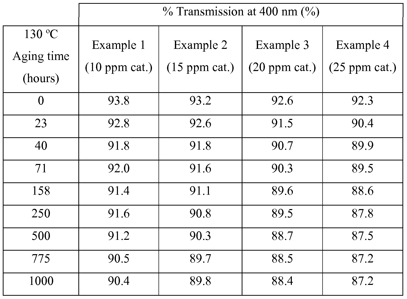
To a 100 mL amber jar was added 40.0 g of the silicone master batch and 20 μL of the catalyst solution (equivalent to 10 ppm platinum catalyst). The solution was mixed thoroughly with a metal spatula and was allowed to degas over several hours. Once the composition was degassed 6.2 g of the solution was poured into a plastic Petri dish having a diameter of 55 mm. The silicone solution was allowed to settle and was then cured by irradiation for 15 minutes under a UVP Blak-Ray Lamp Model XX- 15L fitted with two 16 inch Philips TUV 15 W/G15 T8 Germicidal bulbs emitting primarily at 254 nm, followed by heating for 30 minutes at 80 0C in a forced air oven. The material cures to a tack-free solid in 1 to 2 minutes. The cured silicone disc was removed from the plastic Petri dish and was 2.7 mm in thickness at the center of the silicone disc. A transmission spectrum of the silicone was taken using a PerkinElmer Lambda 900 UV7VIS Spectrophotometer (PerkinElmer Instruments, Norwalk, CT). The transmission of the sample at 400 nm, not corrected for Fresnel reflections, was 93.8%. The sample was placed into a glass Petri dish to protect the surface from contamination by dust and debris and the sample was aged at 130 0C in a forced air oven for 1000 hours. Transmission data for the sample at 400 nm measured during the 1000 hour aging experiment are shown in Table 1. Transmission data for the sample at 460 nm measured during the 1000 hour aging experiment are shown in Table 3. Transmission data for the sample at 530 nm measured during the 1000 hour aging experiment are shown in Table 5. Transmission data for the sample at 670 nm measured during the 1000 hour aging experiment are shown in Table 7.
Example 2
To a 100 mL amber jar was added 40.0 g of the silicone master batch and 30 μL of the catalyst solution (equivalent to 15 ppm platinum catalyst). The solution was mixed thoroughly with a metal spatula and was allowed to degas over several hours. Once the composition was degassed 6.2 g of the solution was poured into a plastic Petri dish having a diameter of 55 mm. The silicone solution was allowed to settle and was then cured by irradiation for 15 minutes under a UVP Blak-Ray Lamp Model XX- 15L fitted with two 16 inch Philips TUV 15 W/G15 T8 Germicidal bulbs emitting primarily at 254 nm, followed by heating for 30 minutes at 80 0C in a forced air oven. The cured silicone disc was removed from the plastic Petri dish and was 2.7 mm in thickness at the center of the silicone disc. A transmission spectrum of the silicone was taken using a PerkinElmer Lambda 900 UV7VIS Spectrophotometer (PerkinElmer Instruments, Norwalk, CT). The transmission of the sample at 400 nm, not corrected for Fresnel reflections, was 93.2%.
The sample was placed into a glass Petri dish to protect the surface from contamination by dust and debris and the sample was aged at 130 0C in a forced air oven for 1000 hours. Transmission data for the sample at 400 nm measured during the 1000 hour aging experiment are shown in Table 1. Transmission data for the sample at 460 nm measured during the 1000 hour aging experiment are shown in Table 3. Transmission data for the sample at 530 nm measured during the 1000 hour aging experiment are shown in Table 5. Transmission data for the sample at 670 nm measured during the 1000 hour aging experiment are shown in Table 7.
Example 3
To a 100 mL amber jar was added 40.0 g of the silicone master batch and 40 μL of the catalyst solution (equivalent to 20 ppm platinum catalyst). The solution was mixed thoroughly with a metal spatula and was allowed to degas over several hours. Once the composition was degassed 6.2 g of the solution was poured into a plastic Petri dish having a diameter of 55 mm. The silicone solution was allowed to settle and was then cured by irradiation for 15 minutes under a UVP Blak-Ray Lamp Model XX- 15L fitted with two 16 inch Philips TUV 15 W/G15 T8 Germicidal bulbs emitting primarily at 254nm, followed by heating for 30 minutes at 80 0C in a forced air oven. The cured silicone disc was removed from the plastic Petri dish and was 2.7 mm in thickness at the center of the silicone disc. A transmission spectrum of the silicone was taken using a PerkinElmer Lambda 900 UV7VIS Spectrophotometer (PerkinElmer Instruments, Norwalk, CT). The transmission of the sample at 400 nm, not corrected for Fresnel reflections, was 92.6%.
The sample was placed into a glass Petri dish to protect the surface from contamination by dust and debris and the sample was aged at 130 0C in a forced air oven for 1000 hours. Transmission data for the sample at 400 nm measured during the 1000 hour aging experiment are shown in Table 1. Transmission data for the sample at 460 nm measured during the 1000 hour aging experiment are shown in Table 3. Transmission data for the sample at 530 nm measured during the 1000 hour aging experiment are shown in Table 5. Transmission data for the sample at 670 nm measured during the 1000 hour aging experiment are shown in Table 7.
Example 4
To a 100 mL amber jar was added 20.0 g of the silicone master batch and 25 μL of the catalyst solution (equivalent to 25 ppm platinum catalyst). The solution was mixed thoroughly with a metal spatula and was allowed to degas over several hours. Once the composition was degassed 6.2 g of the solution was poured into a plastic Petri dish having a diameter of 55 mm. The silicone solution was allowed to settle and was then cured by irradiation for 15 minutes under a UVP Blak-Ray Lamp Model XX- 15L fitted with two 16 inch Philips TUV 15 W/G15 T8 Germicidal bulbs emitting primarily at 254nm, followed by heating for 30 minutes at 80 0C in a forced air oven. The cured silicone disc was removed from the plastic Petri dish and was 2.7 mm in thickness at the center of the silicone disc. A transmission spectrum of the silicone was taken using a PerkinElmer
Lambda 900 UV7VIS Spectrophotometer (PerkinElmer Instruments, Norwalk, CT). The transmission of the sample at 400 nm, not corrected for Fresnel reflections, was 92.3%. The sample was placed into a glass Petri dish to protect the surface from contamination by dust and debris and the sample was aged at 130 0C in a forced air oven for 1000 hours. Transmission data for the sample at 400 nm measured during the 1000 hour aging experiment are shown in Table 1. Transmission data for the sample at 460 nm measured during the 1000 hour aging experiment are shown in Table 3. Transmission data for the sample at 530 nm measured during the 1000 hour aging experiment are shown in Table 5. Transmission data for the sample at 670 nm measured during the 1000 hour aging experiment are shown in Table 7. By extrapolation of the results from Examples 1-4, the composition containing 30 ppm platinum would be expected to have a percent transmission at 400 nm, after 1000 hours at 1300C, of at least about 85%.
Comparative Example 1
To a 100 mL amber jar was added 20.0 g of the silicone master batch and 50 μL of the catalyst solution (equivalent to 50 ppm platinum catalyst). The solution was mixed thoroughly with a metal spatula and was allowed to degas over several hours. Once the composition was degassed 6.2 g of the solution was poured into a plastic Petri dish having a diameter of 55 mm. The silicone solution was allowed to settle and was then cured by irradiation for 15 minutes under a UVP Blak-Ray Lamp Model XX- 15L fitted with two 16 inch Philips TUV 15 W/G15 T8 Germicidal bulbs emitting primarily at 254 nm, followed by heating for 30 minutes at 80 0C in a forced air oven. The material cures to a tack-free solid in about 1 minute. The cured silicone disc was removed from the plastic Petri dish and was 2.7 mm in thickness at the center of the silicone disc. A transmission spectrum of the silicone was taken using a PerkinElmer Lambda 900 UV7VIS Spectrophotometer (PerkinElmer Instruments, Norwalk, CT). The transmission of the sample at 400 nm, not corrected for Fresnel reflections, was 88.9%. The sample was placed into a glass Petri dish to protect the surface from contamination by dust and debris and the sample was aged at 130 0C in a forced air oven for 1000 hours. Transmission data for the sample at 400 nm measured during the 1000 hour aging experiment are shown in Table 2. Transmission data for the sample at 460 nm measured during the 1000 hour aging experiment are shown in Table 4. Transmission data for the sample at 530 nm measured during the 1000 hour aging experiment are shown in Table 6. Transmission data for the sample at 670 nm measured during the 1000 hour aging experiment are shown in Table 8. Comparative Example 2
To a 100 mL amber jar was added 20.0 g of the silicone master batch and 100 μL of the catalyst solution (equivalent to 100 ppm platinum catalyst). The solution was mixed thoroughly with a metal spatula and was allowed to degas over several hours. Once the composition was degassed 6.2 g of the solution was poured into a plastic Petri dish having a diameter of 55 mm. The silicone solution was allowed to settle and was then cured by irradiation for 15 minutes under a UVP Blak-Ray Lamp Model XX- 15L fitted with two 16 inch Philips TUV 15 W/G15 T8 Germicidal bulbs emitting primarily at 254 nm, followed by heating for 30 minutes at 80 0C in a forced air oven. The cured silicone disc was removed from the plastic Petri dish and was 2.7 mm in thickness at the center of the silicone disc. A transmission spectrum of the silicone was taken using a PerkinElmer Lambda 900 UV7VIS Spectrophotometer (PerkinElmer Instruments, Norwalk, CT). The transmission of the sample at 400 nm, not corrected for Fresnel reflections, was 84.6%. The sample was placed into a glass Petri dish to protect the surface from contamination by dust and debris and the sample was aged at 130 0C in a forced air oven for 1000 hours. Transmission data for the sample at 400 nm measured during the 1000 hour aging experiment are shown in Table 2. Transmission data for the sample at 460 nm measured during the 1000 hour aging experiment are shown in Table 4. Transmission data for the sample at 530 nm measured during the 1000 hour aging experiment are shown in Table 6. Transmission data for the sample at 670 nm measured during the 1000 hour aging experiment are shown in Table 8.
Comparative Example 3 To a 100 mL amber jar was added 20.0 g of the silicone master batch and 200 μL of the catalyst solution (equivalent to 200 ppm platinum catalyst). The solution was mixed thoroughly with a metal spatula and was allowed to degas over several hours. Once the composition was degassed 6.2 g of the solution was poured into a plastic Petri dish having a diameter of 55 mm. The silicone solution was allowed to settle and was then cured by irradiation for 15 minutes under a UVP Blak-Ray Lamp Model XX-15L fitted with two 16 inch Philips TUV 15 W/G15 T8 Germicidal bulbs emitting primarily at 254 nm, followed by heating for 30 minutes at 80 0C in a forced air oven. The cured silicone disc was removed from the plastic Petri dish and was 2.7 mm in thickness at the center of the silicone disc. A transmission spectrum of the silicone was taken using a PerkinElmer Lambda 900 UV7VIS Spectrophotometer (PerkinElmer Instruments, Norwalk, CT). The transmission of the sample at 400 nm, not corrected for Fresnel reflections, was 79.4%. The sample was placed into a glass Petri dish to protect the surface from contamination by dust and debris and the sample was aged at 130 0C in a forced air oven for 1000 hours. Transmission data for the sample at 400 nm measured during the 1000 hour aging experiment are shown in Table 2. Transmission data for the sample at 460 nm measured during the 1000 hour aging experiment are shown in Table 4. Transmission data for the sample at 530 nm measured during the 1000 hour aging experiment are shown in Table 6. Transmission data for the sample at 670 nm measured during the 1000 hour aging experiment are shown in Table 8.
Table 1
Figure imgf000026_0001
Table 2
Figure imgf000027_0001
Table 3
Figure imgf000027_0002
Table 4
% Transmission at 460 nm
Figure imgf000028_0001
Table 5
Figure imgf000028_0002
Table 6
Figure imgf000029_0001
Table 7
Figure imgf000029_0002
Table 8
% Transmission at 670 nm
Figure imgf000030_0001
Various modifications and alterations to the invention will become apparent to those skilled in the art without departing from the scope and spirit of the invention.

Claims

What is claimed is:
1. An optical article comprising: a photopolymerizable composition disposed on a major surface of a substrate, wherein the photopolymerizable composition comprises: a silicon-containing resin comprising silicon-bonded hydrogen and aliphatic unsaturation, and a platinum catalyst providing from about 0.5 to about 30 parts per million of platinum; and the major surface imparts a positive or negative lens to the photopolymerizable composition.
2. The optical article of claim 1, wherein the photopolymerizable composition is free of catalyst inhibitor.
3. The optical article of claim 1, wherein the silicon-containing resin comprises an organosiloxane.
4. The optical article of claim 1, wherein the silicon-containing resin comprises a first organosiloxane having units of the formula: R1 aHcSi0(4-a-c)/2 wherein:
R1 is a monovalent, straight-chained, branched or cyclic, unsubstituted or substituted, hydrocarbon group that is free of aliphatic unsaturation and has from 1 to 18 carbon atoms; a is 0, 1, 2, or 3; c is 0, 1, or 2; and the sum of a+c is 0, 1, 2, or 3; with the proviso that there is on average at least one silicon-bonded hydrogen present per molecule.
5. The optical article of claim 1, wherein the silicon-containing resin comprises a second organosiloxane, the second organosiloxane having units of the formula:
Figure imgf000032_0001
wherein:
R1 is a monovalent, straight-chained, branched or cyclic, unsubstituted or substituted, hydrocarbon group that is free of aliphatic unsaturation and has from 1 to 18 carbon atoms;
R2 is a monovalent hydrocarbon group having aliphatic unsaturation and from 2 to 10 carbon atoms; a is 0, 1, 2, or 3; b is 0, 1, 2, or 3; and the sum a+b is 0, 1, 2, or 3; with the proviso that there is on average at least one R2 present per molecule.
6. The optical article of claim 1, wherein the positive or negative lens is a Fresnel lens.
7. The optical article of claim 1, wherein the substrate is transparent.
8. The optical article of claim 1, wherein the substrate comprises a pressure sensitive adhesive.
9. The optical article of claim 8, wherein the pressure sensitive adhesive is formed from free-radically polymerizable monomers selected from the group of (meth)acrylates, vinyl monomers, and mixtures thereof.
10. The optical article of claim 8, wherein the pressure sensitive adhesive is formed from a (meth)acrylate block copolymer comprising: at least two A block polymeric units that are the reaction product of a first monomer composition comprising an alkyl methacrylate, an aralkyl methacrylate, an aryl methacrylate, or a combination thereof, each A block having a Tg of at least 5O0C, the methacrylate block copolymer comprising from 20 to 50 weight percent A block; and at least one B block polymeric unit that is the reaction product of a second monomer composition comprising an alkyl (meth)acrylate, a heteroalkyl (meth)acrylate, a vinyl ester, or a combination thereof, the B block having a Tg no greater than 2O0C, the (meth)acrylate block copolymer comprising from 50 to 80 weight percent B block; wherein the A block polymeric units are present as nanodomains having an average size less than about 150 nm in a matrix of the B block polymeric units.
11. The optical article of claim 8, wherein the pressure sensitive adhesive comprises a silicone-based pressure sensitive adhesive.
12. The optical article of claim 1, further comprising a curable adhesive-forming composition disposed on the photopolymerizable composition.
13. A method of making an optical article, comprising: providing a photopolymerizable composition disposed on a major surface of a first substrate, wherein the photopolymerizable composition comprises: a silicon-containing resin comprising silicon-bonded hydrogen and aliphatic unsaturation, and a platinum catalyst providing from about 0.5 to about 30 parts per million of platinum; and the major surface imparts a positive or negative lens to the photopolymerizable composition; and photopolymerizing the photopolymerizable composition to form a photopolymerized composition, wherein photopolymerizing comprises applying actinic radiation having a wavelength of 700 nm or less.
14. The method of claim 13, wherein the actinic radiation has a wavelength of from 250 to 500 nm.
15. The method of claim 13, further comprising separating the photopolymerized composition from the first substrate.
16. An optical article prepared according to the method of claim 15.
17. The method of claim 14, further comprising: providing a second substrate disposed on the photopolymerizable composition.
18. The method of claim 17, further comprising separating the photopolymerized composition from the first substrate.
19. An optical article prepared according to the method of claim 18.
20. The method of claim 13, further comprising: forming a curable adhesive-forming composition disposed on the photopolymerizable composition; photopolymerizing the photopolymerizable composition to form a photopolymerized composition, wherein photopolymerizing comprises applying actinic radiation having a wavelength of 700 nm or less; and polymerizing the curable adhesive-forming composition to form a pressure sensitive adhesive.
21. The method of claim 20, wherein the actinic radiation has a wavelength of from 250 to 500 nm.
22. The method of claim 20, wherein the pressure sensitive adhesive comprises a silicone-based pressure sensitive adhesive.
23. The method of claim 22, wherein polymerizing the curable adhesive-forming composition to form a pressure sensitive adhesive comprising photopolymerizing the curable adhesive-forming composition.
24. The method of claim 20, further comprising separating the photopolymerized composition from the first substrate.
25. An optical article prepared according to the method of claim 20.
PCT/US2008/052742 2007-02-13 2008-02-01 Molded optical articles and methods of making same WO2008100719A1 (en)

Priority Applications (3)

Application Number Priority Date Filing Date Title
JP2009549661A JP2010519573A (en) 2007-02-13 2008-02-01 Molded optical article and manufacturing method thereof
EP08714157A EP2111645A4 (en) 2007-02-13 2008-02-01 Molded optical articles and methods of making same
CN2008800048785A CN101627477B (en) 2007-02-13 2008-02-01 Molded optical articles and methods of making same

Applications Claiming Priority (4)

Application Number Priority Date Filing Date Title
US88962707P 2007-02-13 2007-02-13
US60/889,627 2007-02-13
US12/018,298 US9944031B2 (en) 2007-02-13 2008-01-23 Molded optical articles and methods of making same
US12/018,298 2008-01-23

Publications (1)

Publication Number Publication Date
WO2008100719A1 true WO2008100719A1 (en) 2008-08-21

Family

ID=41556914

Family Applications (1)

Application Number Title Priority Date Filing Date
PCT/US2008/052742 WO2008100719A1 (en) 2007-02-13 2008-02-01 Molded optical articles and methods of making same

Country Status (7)

Country Link
US (1) US9944031B2 (en)
EP (1) EP2111645A4 (en)
JP (2) JP2010519573A (en)
KR (1) KR20090115802A (en)
CN (2) CN101627477B (en)
TW (1) TWI533022B (en)
WO (1) WO2008100719A1 (en)

Cited By (3)

* Cited by examiner, † Cited by third party
Publication number Priority date Publication date Assignee Title
JP2009190300A (en) * 2008-02-15 2009-08-27 Toppan Printing Co Ltd Imprint device and imprint method
EP3086145A4 (en) * 2013-12-20 2017-09-06 LG Chem, Ltd. Optical film
US11047537B2 (en) 2017-05-02 2021-06-29 Signify Holding B.V. Fixing of LED strips

Families Citing this family (76)

* Cited by examiner, † Cited by third party
Publication number Priority date Publication date Assignee Title
US9070850B2 (en) 2007-10-31 2015-06-30 Cree, Inc. Light emitting diode package and method for fabricating same
US9711703B2 (en) 2007-02-12 2017-07-18 Cree Huizhou Opto Limited Apparatus, system and method for use in mounting electronic elements
JPWO2009101883A1 (en) * 2008-02-13 2011-06-09 コニカミノルタオプト株式会社 Method for manufacturing hybrid optical element assembly
US9123614B2 (en) 2008-10-07 2015-09-01 Mc10, Inc. Methods and applications of non-planar imaging arrays
US8389862B2 (en) 2008-10-07 2013-03-05 Mc10, Inc. Extremely stretchable electronics
EP2349440B1 (en) 2008-10-07 2019-08-21 Mc10, Inc. Catheter balloon having stretchable integrated circuitry and sensor array
US8097926B2 (en) 2008-10-07 2012-01-17 Mc10, Inc. Systems, methods, and devices having stretchable integrated circuitry for sensing and delivering therapy
US8886334B2 (en) 2008-10-07 2014-11-11 Mc10, Inc. Systems, methods, and devices using stretchable or flexible electronics for medical applications
EP2398629A4 (en) * 2009-02-17 2016-06-08 Univ Illinois Methods for fabricating microstructures
TW201101520A (en) * 2009-06-25 2011-01-01 Atomic Energy Council Solar cell module condenser
WO2011041727A1 (en) 2009-10-01 2011-04-07 Mc10, Inc. Protective cases with integrated electronics
DE102010002141A1 (en) * 2010-02-19 2011-08-25 Momentive Performance Materials GmbH, 51373 Integral Irradiation Unit
CN104681694B (en) * 2010-08-18 2017-08-08 晶元光电股份有限公司 Light-emitting device
JP5490671B2 (en) * 2010-12-07 2014-05-14 信越化学工業株式会社 Method for curing silicone resin composition
TWI441361B (en) * 2010-12-31 2014-06-11 Interlight Optotech Corp Light emitting diode packaging structure and method for fabricating the same
CN102650710A (en) * 2011-02-25 2012-08-29 富士康(昆山)电脑接插件有限公司 Optical waveguide structure and manufacturing method thereof
JP5840377B2 (en) 2011-04-14 2016-01-06 日東電工株式会社 Reflective resin sheet and method for manufacturing light-emitting diode device
WO2012160769A1 (en) * 2011-05-24 2012-11-29 コニカミノルタアドバンストレイヤー株式会社 Method for manufacturing resin molded article
JP2014523633A (en) 2011-05-27 2014-09-11 エムシー10 インコーポレイテッド Electronic, optical and / or mechanical devices and systems and methods of manufacturing these devices and systems
CN102881801B (en) * 2011-07-12 2015-10-21 宏齐科技股份有限公司 Back of the body cut package structure for LED and preparation method thereof
WO2013022853A1 (en) 2011-08-05 2013-02-14 Mc10, Inc. Catheter balloon methods and apparatus employing sensing elements
US9757050B2 (en) 2011-08-05 2017-09-12 Mc10, Inc. Catheter balloon employing force sensing elements
US20130200268A1 (en) * 2011-09-28 2013-08-08 Mc10, Inc. Electronics for detection of a property of a surface
JP2013087199A (en) 2011-10-18 2013-05-13 Shin-Etsu Chemical Co Ltd Method of curing addition curable organopolysiloxane composition
US8564004B2 (en) * 2011-11-29 2013-10-22 Cree, Inc. Complex primary optics with intermediate elements
CN103137826B (en) * 2011-11-30 2016-03-23 展晶科技(深圳)有限公司 Light-emitting diode
WO2013109607A1 (en) * 2012-01-16 2013-07-25 Dow Corning Corporation Optical article and method of forming
EP2812738B1 (en) 2012-02-09 2016-10-12 Dow Corning Corporation Gradient polymer structures and methods
DE102012008639A1 (en) * 2012-05-02 2013-11-07 Heraeus Noblelight Gmbh Method for producing an optical module with a silicone optic
DE102012008640A1 (en) * 2012-05-02 2013-11-07 Heraeus Noblelight Gmbh Method for producing an optical module with a polymer optic
CN103474562B (en) * 2012-06-08 2016-11-23 展晶科技(深圳)有限公司 The manufacture method of light emitting diode
EP2858803B1 (en) 2012-06-11 2018-08-29 Momentive Performance Materials GmbH Method for producing plastic composite molded bodies
US9226402B2 (en) 2012-06-11 2015-12-29 Mc10, Inc. Strain isolation structures for stretchable electronics
US9295842B2 (en) 2012-07-05 2016-03-29 Mc10, Inc. Catheter or guidewire device including flow sensing and use thereof
WO2014007871A1 (en) 2012-07-05 2014-01-09 Mc10, Inc. Catheter device including flow sensing
US9171794B2 (en) 2012-10-09 2015-10-27 Mc10, Inc. Embedding thin chips in polymer
KR20150072415A (en) 2012-10-09 2015-06-29 엠씨10, 인크 Conformal electronics integrated with apparel
US9470395B2 (en) 2013-03-15 2016-10-18 Abl Ip Holding Llc Optic for a light source
US10807329B2 (en) * 2013-05-10 2020-10-20 Abl Ip Holding Llc Silicone optics
US9706647B2 (en) 2013-05-14 2017-07-11 Mc10, Inc. Conformal electronics including nested serpentine interconnects
KR20160040670A (en) 2013-08-05 2016-04-14 엠씨10, 인크 Flexible temperature sensor including conformable electronics
CA2925387A1 (en) 2013-10-07 2015-04-16 Mc10, Inc. Conformal sensor systems for sensing and analysis
DE102013220960A1 (en) * 2013-10-16 2015-04-30 Osram Opto Semiconductors Gmbh Optoelectronic component and method for its production
CN105813545A (en) 2013-11-22 2016-07-27 Mc10股份有限公司 Conformal sensor systems for sensing and analysis of cardiac activity
WO2015103580A2 (en) 2014-01-06 2015-07-09 Mc10, Inc. Encapsulated conformal electronic systems and devices, and methods of making and using the same
JP6637896B2 (en) 2014-03-04 2020-01-29 エムシー10 インコーポレイテッドMc10,Inc. Conformal IC device with flexible multi-part encapsulated housing for electronic devices
US9601670B2 (en) 2014-07-11 2017-03-21 Cree, Inc. Method to form primary optic with variable shapes and/or geometries without a substrate
US9899330B2 (en) 2014-10-03 2018-02-20 Mc10, Inc. Flexible electronic circuits with embedded integrated circuit die
US10297572B2 (en) 2014-10-06 2019-05-21 Mc10, Inc. Discrete flexible interconnects for modules of integrated circuits
USD781270S1 (en) 2014-10-15 2017-03-14 Mc10, Inc. Electronic device having antenna
DE102014116370A1 (en) * 2014-11-10 2016-05-12 Osram Opto Semiconductors Gmbh Method for producing a carrier and method for producing an optoelectronic component
AU2016205433A1 (en) * 2015-01-05 2017-07-27 E-Vision Smart Optics, Inc. Methods and systems for mold releases
US10409078B2 (en) * 2015-01-26 2019-09-10 Omnivision Technologies, Inc. Lensed beam-splitter prism array and associated method
CN107530004A (en) 2015-02-20 2018-01-02 Mc10股份有限公司 The automatic detection and construction of wearable device based on personal situation, position and/or orientation
US10398343B2 (en) 2015-03-02 2019-09-03 Mc10, Inc. Perspiration sensor
US10653332B2 (en) 2015-07-17 2020-05-19 Mc10, Inc. Conductive stiffener, method of making a conductive stiffener, and conductive adhesive and encapsulation layers
JP6553980B2 (en) * 2015-08-13 2019-07-31 株式会社ダイセル Curable composition and cured product thereof
WO2017031129A1 (en) 2015-08-19 2017-02-23 Mc10, Inc. Wearable heat flux devices and methods of use
CN108290070A (en) 2015-10-01 2018-07-17 Mc10股份有限公司 Method and system for interacting with virtual environment
EP3359031A4 (en) 2015-10-05 2019-05-22 Mc10, Inc. Method and system for neuromodulation and stimulation
US10476164B2 (en) 2015-10-28 2019-11-12 Rogers Corporation Broadband multiple layer dielectric resonator antenna and method of making the same
US11367959B2 (en) 2015-10-28 2022-06-21 Rogers Corporation Broadband multiple layer dielectric resonator antenna and method of making the same
EP3420733A4 (en) 2016-02-22 2019-06-26 Mc10, Inc. System, device, and method for coupled hub and sensor node on-body acquisition of sensor information
EP3420732B8 (en) 2016-02-22 2020-12-30 Medidata Solutions, Inc. System, devices, and method for on-body data and power transmission
CN109310340A (en) 2016-04-19 2019-02-05 Mc10股份有限公司 For measuring the method and system of sweat
US10447347B2 (en) 2016-08-12 2019-10-15 Mc10, Inc. Wireless charger and high speed data off-loader
US11283189B2 (en) 2017-05-02 2022-03-22 Rogers Corporation Connected dielectric resonator antenna array and method of making the same
US11876295B2 (en) 2017-05-02 2024-01-16 Rogers Corporation Electromagnetic reflector for use in a dielectric resonator antenna system
EP3424740B1 (en) * 2017-07-05 2022-06-15 The Procter & Gamble Company Method of printing 3d-microoptic images on packing systems
CA3076669A1 (en) 2017-10-17 2019-04-25 Magic Leap, Inc. Methods and apparatuses for casting polymer products
US11616302B2 (en) 2018-01-15 2023-03-28 Rogers Corporation Dielectric resonator antenna having first and second dielectric portions
US11552390B2 (en) 2018-09-11 2023-01-10 Rogers Corporation Dielectric resonator antenna system
US11637377B2 (en) 2018-12-04 2023-04-25 Rogers Corporation Dielectric electromagnetic structure and method of making the same
CN113906066A (en) 2019-05-30 2022-01-07 罗杰斯公司 Photocurable composition for stereolithography, stereolithography method using the same, polymer assembly formed by stereolithography method, and device comprising the polymer assembly
US11482790B2 (en) 2020-04-08 2022-10-25 Rogers Corporation Dielectric lens and electromagnetic device with same
TWI806744B (en) * 2022-08-19 2023-06-21 友達光電股份有限公司 Light source module

Citations (4)

* Cited by examiner, † Cited by third party
Publication number Priority date Publication date Assignee Title
US4632899A (en) * 1983-12-01 1986-12-30 Fuji Photo Film Co., Ltd. Photopolymerizable image-recording process of producing a visible image
US5389698A (en) * 1991-07-26 1995-02-14 Hoffmann-La Roche Inc. Process for making photopolymers having varying molecular orientation using light to orient and polymerize
US5998096A (en) * 1992-06-17 1999-12-07 Nitto Denko Corporation Process for producing polymerization or crosslinking rate-distributed article and process for producing lens, lens array or waveguide using the process
US6770685B1 (en) * 1999-10-19 2004-08-03 Sscp Co., Ltd. Resin composition for manufacturing optical fiber ribbon and method for preparing resin for manufacturing optical fiber ribbon using the same

Family Cites Families (116)

* Cited by examiner, † Cited by third party
Publication number Priority date Publication date Assignee Title
US3220972A (en) * 1962-07-02 1965-11-30 Gen Electric Organosilicon process using a chloroplatinic acid reaction product as the catalyst
US3159662A (en) * 1962-07-02 1964-12-01 Gen Electric Addition reaction
US3410886A (en) * 1965-10-23 1968-11-12 Union Carbide Corp Si-h to c=c or c=c addition in the presence of a nitrile-platinum (ii) halide complex
US4530879A (en) * 1983-03-04 1985-07-23 Minnesota Mining And Manufacturing Company Radiation activated addition reaction
US4510094A (en) * 1983-12-06 1985-04-09 Minnesota Mining And Manufacturing Company Platinum complex
US4585669A (en) * 1984-09-28 1986-04-29 General Electric Company Novel dual cure silicone compositions
US4609574A (en) * 1985-10-03 1986-09-02 Dow Corning Corporation Silicone release coatings containing higher alkenyl functional siloxanes
FR2592221B1 (en) * 1985-12-20 1988-02-12 Radiotechnique Compelec METHOD OF ENCAPSULATING AN ELECTRONIC COMPONENT BY MEANS OF A SYNTHETIC RESIN
US4670531A (en) * 1986-01-21 1987-06-02 General Electric Company Inhibited precious metal catalyzed organopolysiloxane compositions
US5145886A (en) * 1988-05-19 1992-09-08 Minnesota Mining And Manufacturing Company Radiation activated hydrosilation reaction
US5169727A (en) * 1988-08-04 1992-12-08 Minnesota Mining And Manufacturing Company Silicone-based pressure-sensitive adhesives having high solids content
US4916169A (en) * 1988-09-09 1990-04-10 Minnesota Mining And Manufacturing Company Visible radiation activated hydrosilation reaction
US6376569B1 (en) * 1990-12-13 2002-04-23 3M Innovative Properties Company Hydrosilation reaction utilizing a (cyclopentadiene)(sigma-aliphatic) platinum complex and a free radical photoinitiator
US6046250A (en) * 1990-12-13 2000-04-04 3M Innovative Properties Company Hydrosilation reaction utilizing a free radical photoinitiator
GB2252746B (en) * 1991-01-17 1995-07-12 Towa Corp A method of molding resin to seal an electronic part on a lead frame and apparatus therefor
US5248716A (en) * 1992-01-30 1993-09-28 General Electric Company Silicone pressure-sensitive adhesives with control removal property
JP3147481B2 (en) * 1992-04-21 2001-03-19 松下電器産業株式会社 Mold for forming glass diffraction grating, method for manufacturing the same, and method for manufacturing glass diffraction grating
JP3211381B2 (en) * 1992-06-25 2001-09-25 住友化学工業株式会社 Manufacturing method of light control plate
US5300263A (en) * 1992-10-28 1994-04-05 Minnesota Mining And Manufacturing Company Method of making a microlens array and mold
DE4242469A1 (en) * 1992-12-16 1994-06-23 Wacker Chemie Gmbh Catalysts for hydrosilylation reactions
JP2524955B2 (en) * 1993-04-22 1996-08-14 トーワ株式会社 Method and apparatus for resin sealing molding of electronic parts
US5536455A (en) * 1994-01-03 1996-07-16 Omron Corporation Method of manufacturing lens array
JP3423766B2 (en) * 1994-03-11 2003-07-07 Towa株式会社 Resin encapsulation molding method and mold device for electronic components
FR2717481B1 (en) 1994-03-18 1996-06-28 Rhone Poulenc Chimie New platinum complexes useful, in particular, as photoactivatable hydrosilylation catalysts and process for applying them.
JPH07268219A (en) * 1994-03-31 1995-10-17 Toray Dow Corning Silicone Co Ltd Silicone gel composition for optical filling
DE4423195A1 (en) * 1994-07-01 1996-01-04 Wacker Chemie Gmbh Triazenoxide-transition metal complexes as hydrosilylation catalysts
JPH10182770A (en) * 1996-03-13 1998-07-07 Tokuyama Corp Photopolymerization composition and transparent cured product
DE19638667C2 (en) * 1996-09-20 2001-05-17 Osram Opto Semiconductors Gmbh Mixed-color light-emitting semiconductor component with luminescence conversion element
JPH10158349A (en) 1996-11-28 1998-06-16 Dainippon Printing Co Ltd Ionizing radiation-curing type resin composition for optical sheet, optical sheet and its production
US6473554B1 (en) * 1996-12-12 2002-10-29 Teledyne Lighting And Display Products, Inc. Lighting apparatus having low profile
US6274890B1 (en) * 1997-01-15 2001-08-14 Kabushiki Kaisha Toshiba Semiconductor light emitting device and its manufacturing method
JP3609942B2 (en) 1998-06-29 2005-01-12 株式会社巴川製紙所 Optical connecting component and manufacturing method thereof
US6670207B1 (en) * 1999-03-15 2003-12-30 Gentex Corporation Radiation emitter device having an integral micro-groove lens
SE9803481D0 (en) * 1998-10-13 1998-10-13 Pharmacia & Upjohn Ab Photocurable siloxane polymers
US6204523B1 (en) * 1998-11-06 2001-03-20 Lumileds Lighting, U.S., Llc High stability optical encapsulation and packaging for light-emitting diodes in the green, blue, and near UV range
JP2000208822A (en) * 1999-01-11 2000-07-28 Matsushita Electronics Industry Corp Semiconductor light-emitting device
JP3349111B2 (en) 1999-03-15 2002-11-20 株式会社シチズン電子 Surface mount type light emitting diode and method of manufacturing the same
US6808509B1 (en) * 1999-04-22 2004-10-26 Scimed Life Systems, Inc. Valved introducer sheath and related methods
US6150546A (en) * 1999-05-03 2000-11-21 General Electric Company Irradiation-curable silicone compositions, photo-active platinum (IV) compounds, and method
US6367949B1 (en) * 1999-08-04 2002-04-09 911 Emergency Products, Inc. Par 36 LED utility lamp
US6432137B1 (en) * 1999-09-08 2002-08-13 Medennium, Inc. High refractive index silicone for use in intraocular lenses
WO2001074554A2 (en) * 2000-03-31 2001-10-11 Bausch & Lomb Incorporated Method and mold to control optical device polymerization
US6650044B1 (en) 2000-10-13 2003-11-18 Lumileds Lighting U.S., Llc Stenciling phosphor layers on light emitting diodes
DE10051242A1 (en) * 2000-10-17 2002-04-25 Philips Corp Intellectual Pty Light-emitting device with coated phosphor
JP4275890B2 (en) 2001-02-13 2009-06-10 株式会社カネカ Light emitting diode and manufacturing method thereof
US6623667B2 (en) * 2001-02-28 2003-09-23 3M Innovative Properties Company Method for continuous fabrication of structured surface light guides
JP4009067B2 (en) * 2001-03-06 2007-11-14 信越化学工業株式会社 Addition-curing silicone resin composition
US6598998B2 (en) * 2001-05-04 2003-07-29 Lumileds Lighting, U.S., Llc Side emitting light emitting device
FR2825709B1 (en) * 2001-06-07 2005-07-01 Rhodia Chimie Sa HYDROSILYLATION ELASTOMER-CROSS-LINKABLE SILICONE COMPOSITION IN THE PRESENCE OF CARBENE-BASED METAL CATALYSTS AND CATALYSTS OF THIS TYPE
DE10129785B4 (en) * 2001-06-20 2010-03-18 Osram Opto Semiconductors Gmbh Optoelectronic component and method for its production
US6617401B2 (en) * 2001-08-23 2003-09-09 General Electric Company Composition comprising cycloaliphatic epoxy resin, 4-methylhexahydrophthalic anhydride curing agent and boron catalyst
US20030115907A1 (en) * 2001-09-07 2003-06-26 Patton Edward K. Multiple lens molding system and method
US6804062B2 (en) * 2001-10-09 2004-10-12 California Institute Of Technology Nonimaging concentrator lens arrays and microfabrication of the same
JP4009097B2 (en) * 2001-12-07 2007-11-14 日立電線株式会社 LIGHT EMITTING DEVICE, ITS MANUFACTURING METHOD, AND LEAD FRAME USED FOR MANUFACTURING LIGHT EMITTING DEVICE
US6897164B2 (en) 2002-02-14 2005-05-24 3M Innovative Properties Company Aperture masks for circuit fabrication
US20030199603A1 (en) * 2002-04-04 2003-10-23 3M Innovative Properties Company Cured compositions transparent to ultraviolet radiation
US6679621B2 (en) * 2002-06-24 2004-01-20 Lumileds Lighting U.S., Llc Side emitting LED and lens
US20060100299A1 (en) * 2002-07-24 2006-05-11 Ranjit Malik Transformable pressure sensitive adhesive tape and use thereof in display screens
US20050076376A1 (en) * 2002-07-24 2005-04-07 Raymond Lind Video entertainment satellite network system
CN100550430C (en) 2002-09-09 2009-10-14 皇家飞利浦电子股份有限公司 Semiconductor device and manufacture method thereof
US6908682B2 (en) * 2002-09-12 2005-06-21 3M Innovative Properties Company Photocured silicone sealant having improved adhesion to plastic
US6682331B1 (en) * 2002-09-20 2004-01-27 Agilent Technologies, Inc. Molding apparatus for molding light emitting diode lamps
US7143609B2 (en) 2002-10-29 2006-12-05 Corning Incorporated Low-temperature fabrication of glass optical components
US7595113B2 (en) * 2002-11-29 2009-09-29 Shin-Etsu Chemical Co., Ltd. LED devices and silicone resin composition therefor
JP2004186168A (en) * 2002-11-29 2004-07-02 Shin Etsu Chem Co Ltd Silicone resin composition for light emitting diode element
CN100528517C (en) 2002-12-13 2009-08-19 皇家飞利浦电子股份有限公司 Method of manufacturing a replica, as well as a replica obtained by carrying out a UV light-initiated or thermal curing treatment of a reactive mixture
US7245435B2 (en) * 2002-12-16 2007-07-17 3M Innovative Properties Company Lens array sheet and molding method
US7157839B2 (en) * 2003-01-27 2007-01-02 3M Innovative Properties Company Phosphor based light sources utilizing total internal reflection
US20040173808A1 (en) * 2003-03-07 2004-09-09 Bor-Jen Wu Flip-chip like light emitting device package
TW200427111A (en) 2003-03-12 2004-12-01 Shinetsu Chemical Co Material for coating/protecting light-emitting semiconductor and the light-emitting semiconductor device
US7927703B2 (en) * 2003-04-11 2011-04-19 3M Innovative Properties Company Adhesive blends, articles, and methods
US6921929B2 (en) * 2003-06-27 2005-07-26 Lockheed Martin Corporation Light-emitting diode (LED) with amorphous fluoropolymer encapsulant and lens
US20050006659A1 (en) * 2003-07-09 2005-01-13 Ng Kee Yean Light emitting diode utilizing a discrete wavelength-converting layer for color conversion
JP4908736B2 (en) * 2003-10-01 2012-04-04 東レ・ダウコーニング株式会社 Curable organopolysiloxane composition and semiconductor device
JP4503271B2 (en) * 2003-11-28 2010-07-14 東レ・ダウコーニング株式会社 Method for producing silicone laminate
KR100624414B1 (en) * 2003-12-06 2006-09-18 삼성전자주식회사 Manufacturing Method of Diffractive Lens Array and UV Dispenser
JP4801320B2 (en) * 2003-12-19 2011-10-26 東レ・ダウコーニング株式会社 Addition reaction curable organopolysiloxane resin composition
JP2005217369A (en) 2004-02-02 2005-08-11 Three M Innovative Properties Co Adhesive sheet for light-emitting-diode device, and light-emitting-diode device
JP2005248122A (en) 2004-03-08 2005-09-15 Dow Corning Corp Laser light-resistant optical material and laser light-resistant optical element
US7279346B2 (en) * 2004-03-31 2007-10-09 Cree, Inc. Method for packaging a light emitting device by one dispense then cure step followed by another
JP4300418B2 (en) * 2004-04-30 2009-07-22 信越化学工業株式会社 Epoxy / silicone hybrid resin composition and light emitting semiconductor device
JP4875858B2 (en) 2004-05-28 2012-02-15 株式会社朝日ラバー Manufacturing method of lens for semiconductor optical element
WO2005121641A1 (en) 2004-06-11 2005-12-22 Koninklijke Philips Electronics N.V. Illumination system
US7255920B2 (en) * 2004-07-29 2007-08-14 3M Innovative Properties Company (Meth)acrylate block copolymer pressure sensitive adhesives
JP4617761B2 (en) 2004-08-03 2011-01-26 日亜化学工業株式会社 Method for manufacturing light emitting device
JP2006049533A (en) 2004-08-04 2006-02-16 Wacker Asahikasei Silicone Co Ltd Resin sealing light emitting diode device and sealing method
JP2006049657A (en) * 2004-08-06 2006-02-16 Citizen Electronics Co Ltd Led lamp
US7256483B2 (en) 2004-10-28 2007-08-14 Philips Lumileds Lighting Company, Llc Package-integrated thin film LED
US7304425B2 (en) * 2004-10-29 2007-12-04 3M Innovative Properties Company High brightness LED package with compound optical element(s)
JP2006137895A (en) 2004-11-15 2006-06-01 Ge Toshiba Silicones Co Ltd Polyorganosiloxane composition for optical material
US7352011B2 (en) 2004-11-15 2008-04-01 Philips Lumileds Lighting Company, Llc Wide emitting lens for LED useful for backlighting
US7314770B2 (en) 2004-11-18 2008-01-01 3M Innovative Properties Company Method of making light emitting device with silicon-containing encapsulant
US7192795B2 (en) * 2004-11-18 2007-03-20 3M Innovative Properties Company Method of making light emitting device with silicon-containing encapsulant
KR100580753B1 (en) 2004-12-17 2006-05-15 엘지이노텍 주식회사 Light emitting device package
ITRM20040633A1 (en) * 2004-12-23 2005-03-23 St Microelectronics Srl MULTI-SOURCE OPTICAL TRANSMITTER AND PHOTON DISPLAY DEVICE.
US20060138443A1 (en) * 2004-12-23 2006-06-29 Iii-N Technology, Inc. Encapsulation and packaging of ultraviolet and deep-ultraviolet light emitting diodes
TWI261654B (en) * 2004-12-29 2006-09-11 Ind Tech Res Inst Lens and LED with uniform light emitted applying the lens
US7833208B2 (en) * 2004-12-29 2010-11-16 Kimberly-Clark Worldwide, Inc. Multilayer absorbent article
US8012774B2 (en) 2005-01-11 2011-09-06 SemiLEDs Optoelectronics Co., Ltd. Coating process for a light-emitting diode (LED)
US7885003B2 (en) * 2005-01-11 2011-02-08 Dai Nippon Printing Co., Ltd. Optical diffusing sheet, optical deflecting sheet, and transmission type screen
JP4167659B2 (en) * 2005-01-11 2008-10-15 大日本印刷株式会社 Transmission type screen and rear projection type display device
KR101197046B1 (en) * 2005-01-26 2012-11-06 삼성디스플레이 주식회사 Two dimensional light source of using light emitting diode and liquid crystal display panel of using the two dimensional light source
KR20060104432A (en) 2005-03-30 2006-10-09 알티전자 주식회사 Slim type flash device with high brightness
TWI258877B (en) * 2005-05-17 2006-07-21 Young Lighting Technology Inc Method of utilizing the surface mount technology to assemble LED light source, and combination of its LED light source and lens lid
JP5138158B2 (en) * 2005-05-23 2013-02-06 信越化学工業株式会社 Silicone lens molding material for LED light-emitting devices
US20070001182A1 (en) 2005-06-30 2007-01-04 3M Innovative Properties Company Structured phosphor tape article
US7294861B2 (en) * 2005-06-30 2007-11-13 3M Innovative Properties Company Phosphor tape article
JP4717542B2 (en) 2005-07-27 2011-07-06 オリンパスイメージング株式会社 Glass optical element molding equipment
US7365371B2 (en) * 2005-08-04 2008-04-29 Cree, Inc. Packages for semiconductor light emitting devices utilizing dispensed encapsulants
KR100621154B1 (en) 2005-08-26 2006-09-07 서울반도체 주식회사 Manufacturing method of light emitting diode
US20070092736A1 (en) * 2005-10-21 2007-04-26 3M Innovative Properties Company Method of making light emitting device with silicon-containing encapsulant
WO2007050483A2 (en) 2005-10-24 2007-05-03 3M Innovative Properties Company Method of making light emitting device having a molded encapsulant
US7655486B2 (en) * 2006-05-17 2010-02-02 3M Innovative Properties Company Method of making light emitting device with multilayer silicon-containing encapsulant
US7763478B2 (en) * 2006-08-21 2010-07-27 Cree, Inc. Methods of forming semiconductor light emitting device packages by liquid injection molding
TWI434890B (en) * 2007-04-06 2014-04-21 Shinetsu Chemical Co Addition curable silicone resin composition and silicone lens using same
US7960192B2 (en) * 2007-09-14 2011-06-14 3M Innovative Properties Company Light emitting device having silicon-containing composition and method of making same

Patent Citations (4)

* Cited by examiner, † Cited by third party
Publication number Priority date Publication date Assignee Title
US4632899A (en) * 1983-12-01 1986-12-30 Fuji Photo Film Co., Ltd. Photopolymerizable image-recording process of producing a visible image
US5389698A (en) * 1991-07-26 1995-02-14 Hoffmann-La Roche Inc. Process for making photopolymers having varying molecular orientation using light to orient and polymerize
US5998096A (en) * 1992-06-17 1999-12-07 Nitto Denko Corporation Process for producing polymerization or crosslinking rate-distributed article and process for producing lens, lens array or waveguide using the process
US6770685B1 (en) * 1999-10-19 2004-08-03 Sscp Co., Ltd. Resin composition for manufacturing optical fiber ribbon and method for preparing resin for manufacturing optical fiber ribbon using the same

Non-Patent Citations (1)

* Cited by examiner, † Cited by third party
Title
See also references of EP2111645A4 *

Cited By (4)

* Cited by examiner, † Cited by third party
Publication number Priority date Publication date Assignee Title
JP2009190300A (en) * 2008-02-15 2009-08-27 Toppan Printing Co Ltd Imprint device and imprint method
EP3086145A4 (en) * 2013-12-20 2017-09-06 LG Chem, Ltd. Optical film
US10330840B2 (en) 2013-12-20 2019-06-25 Lg Chem, Ltd. Optical film
US11047537B2 (en) 2017-05-02 2021-06-29 Signify Holding B.V. Fixing of LED strips

Also Published As

Publication number Publication date
CN101611502B (en) 2013-06-12
CN101627477A (en) 2010-01-13
JP2014006545A (en) 2014-01-16
US9944031B2 (en) 2018-04-17
EP2111645A4 (en) 2010-07-21
CN101627477B (en) 2011-05-11
TW200842398A (en) 2008-11-01
KR20090115802A (en) 2009-11-06
EP2111645A1 (en) 2009-10-28
US20080193749A1 (en) 2008-08-14
CN101611502A (en) 2009-12-23
JP2010519573A (en) 2010-06-03
TWI533022B (en) 2016-05-11

Similar Documents

Publication Publication Date Title
US9944031B2 (en) Molded optical articles and methods of making same
US8303878B2 (en) Method of making a light emitting device having a molded encapsulant
US8901588B2 (en) LED devices having lenses and methods of making same
US7595515B2 (en) Method of making light emitting device having a molded encapsulant
US20070269586A1 (en) Method of making light emitting device with silicon-containing composition
KR101278415B1 (en) Method of making light emitting device having a molded encapsulant
JP4670669B2 (en) Composite optical component and manufacturing method thereof
US10336025B2 (en) Compound lens for use with illumination sources in optical systems
CN101507003A (en) Method of making a light emitting device having a molded encapsulant
JP5607988B2 (en) Method for manufacturing plastic lens or optical waveguide
JP4714805B2 (en) Microchip
JP5604054B2 (en) Method for manufacturing optical lens or optical waveguide or optical fiber core

Legal Events

Date Code Title Description
WWE Wipo information: entry into national phase

Ref document number: 200880004878.5

Country of ref document: CN

121 Ep: the epo has been informed by wipo that ep was designated in this application

Ref document number: 08714157

Country of ref document: EP

Kind code of ref document: A1

ENP Entry into the national phase

Ref document number: 2009549661

Country of ref document: JP

Kind code of ref document: A

NENP Non-entry into the national phase

Ref country code: DE

WWE Wipo information: entry into national phase

Ref document number: 2008714157

Country of ref document: EP

WWE Wipo information: entry into national phase

Ref document number: 1020097018976

Country of ref document: KR