WO2004047066A2 - Liquid crystal display device - Google Patents
Liquid crystal display device Download PDFInfo
- Publication number
- WO2004047066A2 WO2004047066A2 PCT/IB2003/004829 IB0304829W WO2004047066A2 WO 2004047066 A2 WO2004047066 A2 WO 2004047066A2 IB 0304829 W IB0304829 W IB 0304829W WO 2004047066 A2 WO2004047066 A2 WO 2004047066A2
- Authority
- WO
- WIPO (PCT)
- Prior art keywords
- sequence
- selection
- electrodes
- display device
- time periods
- Prior art date
Links
Classifications
-
- G—PHYSICS
- G09—EDUCATION; CRYPTOGRAPHY; DISPLAY; ADVERTISING; SEALS
- G09G—ARRANGEMENTS OR CIRCUITS FOR CONTROL OF INDICATING DEVICES USING STATIC MEANS TO PRESENT VARIABLE INFORMATION
- G09G3/00—Control arrangements or circuits, of interest only in connection with visual indicators other than cathode-ray tubes
- G09G3/20—Control arrangements or circuits, of interest only in connection with visual indicators other than cathode-ray tubes for presentation of an assembly of a number of characters, e.g. a page, by composing the assembly by combination of individual elements arranged in a matrix no fixed position being assigned to or needed to be assigned to the individual characters or partial characters
- G09G3/34—Control arrangements or circuits, of interest only in connection with visual indicators other than cathode-ray tubes for presentation of an assembly of a number of characters, e.g. a page, by composing the assembly by combination of individual elements arranged in a matrix no fixed position being assigned to or needed to be assigned to the individual characters or partial characters by control of light from an independent source
- G09G3/36—Control arrangements or circuits, of interest only in connection with visual indicators other than cathode-ray tubes for presentation of an assembly of a number of characters, e.g. a page, by composing the assembly by combination of individual elements arranged in a matrix no fixed position being assigned to or needed to be assigned to the individual characters or partial characters by control of light from an independent source using liquid crystals
- G09G3/3611—Control of matrices with row and column drivers
- G09G3/3622—Control of matrices with row and column drivers using a passive matrix
- G09G3/3625—Control of matrices with row and column drivers using a passive matrix using active addressing
-
- G—PHYSICS
- G02—OPTICS
- G02F—OPTICAL DEVICES OR ARRANGEMENTS FOR THE CONTROL OF LIGHT BY MODIFICATION OF THE OPTICAL PROPERTIES OF THE MEDIA OF THE ELEMENTS INVOLVED THEREIN; NON-LINEAR OPTICS; FREQUENCY-CHANGING OF LIGHT; OPTICAL LOGIC ELEMENTS; OPTICAL ANALOGUE/DIGITAL CONVERTERS
- G02F1/00—Devices or arrangements for the control of the intensity, colour, phase, polarisation or direction of light arriving from an independent light source, e.g. switching, gating or modulating; Non-linear optics
- G02F1/01—Devices or arrangements for the control of the intensity, colour, phase, polarisation or direction of light arriving from an independent light source, e.g. switching, gating or modulating; Non-linear optics for the control of the intensity, phase, polarisation or colour
- G02F1/13—Devices or arrangements for the control of the intensity, colour, phase, polarisation or direction of light arriving from an independent light source, e.g. switching, gating or modulating; Non-linear optics for the control of the intensity, phase, polarisation or colour based on liquid crystals, e.g. single liquid crystal display cells
- G02F1/133—Constructional arrangements; Operation of liquid crystal cells; Circuit arrangements
-
- G—PHYSICS
- G09—EDUCATION; CRYPTOGRAPHY; DISPLAY; ADVERTISING; SEALS
- G09G—ARRANGEMENTS OR CIRCUITS FOR CONTROL OF INDICATING DEVICES USING STATIC MEANS TO PRESENT VARIABLE INFORMATION
- G09G3/00—Control arrangements or circuits, of interest only in connection with visual indicators other than cathode-ray tubes
- G09G3/20—Control arrangements or circuits, of interest only in connection with visual indicators other than cathode-ray tubes for presentation of an assembly of a number of characters, e.g. a page, by composing the assembly by combination of individual elements arranged in a matrix no fixed position being assigned to or needed to be assigned to the individual characters or partial characters
- G09G3/34—Control arrangements or circuits, of interest only in connection with visual indicators other than cathode-ray tubes for presentation of an assembly of a number of characters, e.g. a page, by composing the assembly by combination of individual elements arranged in a matrix no fixed position being assigned to or needed to be assigned to the individual characters or partial characters by control of light from an independent source
- G09G3/36—Control arrangements or circuits, of interest only in connection with visual indicators other than cathode-ray tubes for presentation of an assembly of a number of characters, e.g. a page, by composing the assembly by combination of individual elements arranged in a matrix no fixed position being assigned to or needed to be assigned to the individual characters or partial characters by control of light from an independent source using liquid crystals
- G09G3/3611—Control of matrices with row and column drivers
- G09G3/3622—Control of matrices with row and column drivers using a passive matrix
-
- G—PHYSICS
- G09—EDUCATION; CRYPTOGRAPHY; DISPLAY; ADVERTISING; SEALS
- G09G—ARRANGEMENTS OR CIRCUITS FOR CONTROL OF INDICATING DEVICES USING STATIC MEANS TO PRESENT VARIABLE INFORMATION
- G09G3/00—Control arrangements or circuits, of interest only in connection with visual indicators other than cathode-ray tubes
- G09G3/20—Control arrangements or circuits, of interest only in connection with visual indicators other than cathode-ray tubes for presentation of an assembly of a number of characters, e.g. a page, by composing the assembly by combination of individual elements arranged in a matrix no fixed position being assigned to or needed to be assigned to the individual characters or partial characters
- G09G3/34—Control arrangements or circuits, of interest only in connection with visual indicators other than cathode-ray tubes for presentation of an assembly of a number of characters, e.g. a page, by composing the assembly by combination of individual elements arranged in a matrix no fixed position being assigned to or needed to be assigned to the individual characters or partial characters by control of light from an independent source
- G09G3/36—Control arrangements or circuits, of interest only in connection with visual indicators other than cathode-ray tubes for presentation of an assembly of a number of characters, e.g. a page, by composing the assembly by combination of individual elements arranged in a matrix no fixed position being assigned to or needed to be assigned to the individual characters or partial characters by control of light from an independent source using liquid crystals
- G09G3/3611—Control of matrices with row and column drivers
- G09G3/3648—Control of matrices with row and column drivers using an active matrix
-
- G—PHYSICS
- G09—EDUCATION; CRYPTOGRAPHY; DISPLAY; ADVERTISING; SEALS
- G09G—ARRANGEMENTS OR CIRCUITS FOR CONTROL OF INDICATING DEVICES USING STATIC MEANS TO PRESENT VARIABLE INFORMATION
- G09G2320/00—Control of display operating conditions
- G09G2320/02—Improving the quality of display appearance
- G09G2320/0247—Flicker reduction other than flicker reduction circuits used for single beam cathode-ray tubes
-
- G—PHYSICS
- G09—EDUCATION; CRYPTOGRAPHY; DISPLAY; ADVERTISING; SEALS
- G09G—ARRANGEMENTS OR CIRCUITS FOR CONTROL OF INDICATING DEVICES USING STATIC MEANS TO PRESENT VARIABLE INFORMATION
- G09G2330/00—Aspects of power supply; Aspects of display protection and defect management
- G09G2330/02—Details of power systems and of start or stop of display operation
- G09G2330/021—Power management, e.g. power saving
-
- G—PHYSICS
- G09—EDUCATION; CRYPTOGRAPHY; DISPLAY; ADVERTISING; SEALS
- G09G—ARRANGEMENTS OR CIRCUITS FOR CONTROL OF INDICATING DEVICES USING STATIC MEANS TO PRESENT VARIABLE INFORMATION
- G09G3/00—Control arrangements or circuits, of interest only in connection with visual indicators other than cathode-ray tubes
- G09G3/20—Control arrangements or circuits, of interest only in connection with visual indicators other than cathode-ray tubes for presentation of an assembly of a number of characters, e.g. a page, by composing the assembly by combination of individual elements arranged in a matrix no fixed position being assigned to or needed to be assigned to the individual characters or partial characters
- G09G3/2007—Display of intermediate tones
- G09G3/2018—Display of intermediate tones by time modulation using two or more time intervals
- G09G3/2022—Display of intermediate tones by time modulation using two or more time intervals using sub-frames
- G09G3/2025—Display of intermediate tones by time modulation using two or more time intervals using sub-frames the sub-frames having all the same time duration
Definitions
- the invention relates to a display device comprising a liquid crystal material between a first substrate provided with row or selection electrodes and a second substrate provided with column or data electrodes, in which overlapping parts of the row and column electrodes define picture elements, drive means for driving the column electrodes in conformity with an image to be displayed, and drive means for driving the row electrodes.
- display devices are used in, for example, portable apparatuses such as laptop computers, notebook computers and telephones.
- Passive-matrix displays of this type are generally known and are generally driven by providing the row or selection electrodes with selecting voltages and simultaneously supplying data voltages to the column or data electrodes as described by Alt & Pleshko in IEEE Trans El. Dev. Vol. ED -21, No. 2, Feb 1974, ppl46 -155.
- passive-matrix displays are increasingly based on the STN (Super- Twisted Nematic) effect.
- STN Super- Twisted Nematic
- Display cells based on the STN (Super-Twisted Nematic) effect generally have a very steep transmission voltage characteristic, which makes it difficult to realize gray levels.
- One method is sub-pixellation which goes at the cost of the maximum number of lines.
- Another method is "frame rate control" (FRC) which is a technique to generate different gray values by varying the state of a picture element between ON and OFF within a certain number of consecutive frame periods.
- FRC frame rate control
- a frame period is the period in which all rows are selected one time, be it separately (Alt & Pleshko) or in groups (MRA). Thanks to the persistency of the human vision system and the properties of the liquid crystal, the different states are averaged and perceived as one gray value.
- an object of the invention to provide a display device of the type described above, in which flicker is minimized.
- a further purpose of the invention is to provide a display device of the type described above, in which the power used is lowered as compared to existing devices.
- a device according to the invention has drive means comprising means for driving a group of picture elements during time periods within a sequence of time periods, the driving of different picture elements within a sequence of time periods being phase-shifted with respect to each other
- a phase in this Patent Application is understood to be the number of a sub- selection period in a sequence of time periods, when considering the total number of sequences, in this case the number of the position of the phase in a super-frame. In fact it specifies the (sub)-selection period at which a picture element or a group of picture elements is selected. Similar remarks apply to selecting a picture element or a group of picture elements during selection of a sub-selection time in subsequent sequences of selection times.
- the invention is based inter alia on the insight that non-sequential selections of time periods within a sequence of time periods leads to different periodical driving (or even non-periodical driving) of different picture elements.
- the human vision system more easily averages different states now, which are perceived as one gray value.
- phase shifting may be altered after each sequence of time periods.
- the invention is based on the insight that by using a special grayscale table the number of voltage transitions in a driver may be diminished.
- a special embodiment of the invention therefore comprises a grayscale table for generating graylevel data in which grayscale table sequences of s s >1) sequential graylevels are defined by grouping s sequential graylevels within a sequence, said sequences being allotted to non-sequential selections of time periods within a sequence of time periods.
- s-l increases (or decreases) of the number of selections within a sequence of selections are allotted to one time period only.
- Said time period may comply with a frame period in which a sequence of time periods is a sequence of frame periods.
- a preferred embodiment of a device according to the invention in this case comprises means to change the frame-phase of a frame during selection of said frame in subsequent sequences of frame periods.
- phase shifting may also be applied to the driving of active matrix LCDs in which switching means for connecting the picture electrodes to the selection electrodes and data electrodes are provided on a first substrate.
- gray-values are generated by generating analogue voltages e.g. via a resistor chain.
- the analogue voltages are then buffered (e.g. one buffer per gray-value) in an output buffer. If one needs 6 bit per color, that is 64 gray-values per color (256 for 8 bit) 64 buffers (256 for 8 bit) are needed.
- grey- values can be generated by using time averaging between two gray-values, e.g. 4 (or 8).
- the number of generated voltages via the resistor chain can be reduced and hence also the number of buffers in the output stage.
- the output stage becomes smaller which reduces the driver cost whereas having less number of buffers reduces the power consumption of the display driver.
- Figure 1 shows an electric equivalent circuit diagram of a part of a display device in which the invention is used
- Figure 2 shows selection and data voltages for a display device according to Figure 1
- Figure 3 shows a set of picture elements having certain gray-levels
- Figure 4 schematically shows one way of driving these picture elements to display said gray-levels
- Figure 5 shows an electric equivalent circuit diagram of a part of another display device in which the invention is used.
- Figures 6 and 7 show selection and data voltages for a display device according to Figure 5.
- Figure 1 is an electric equivalent circuit diagram of a part of a display device 1 to which the invention is applicable. It comprises a matrix of picture elements 8 defined by the areas of crossings of m row or selection electrodes 7 and n column or data electrodes 6.
- the row electrodes in one mode of driving, are consecutively selected by means of a row driver 4, while the column electrodes are provided with data via a data register 5.
- incoming data 2 are first processed, if necessary, in a processor 3.
- Mutual synchronization between the row driver 4 and the data register 5 takes place via drive lines 9.
- a first method to drive the display device 1 by selecting all rows sequentially (or non-sequentially) by selecting one line at a time (Alt & Pleshko addressing).
- the period over which all lines are selected is called a frame (time).
- Using multiple frames it is possible to generate gray-levels.
- the number of frames in which a grayscale is defined is indicated as a superframe.
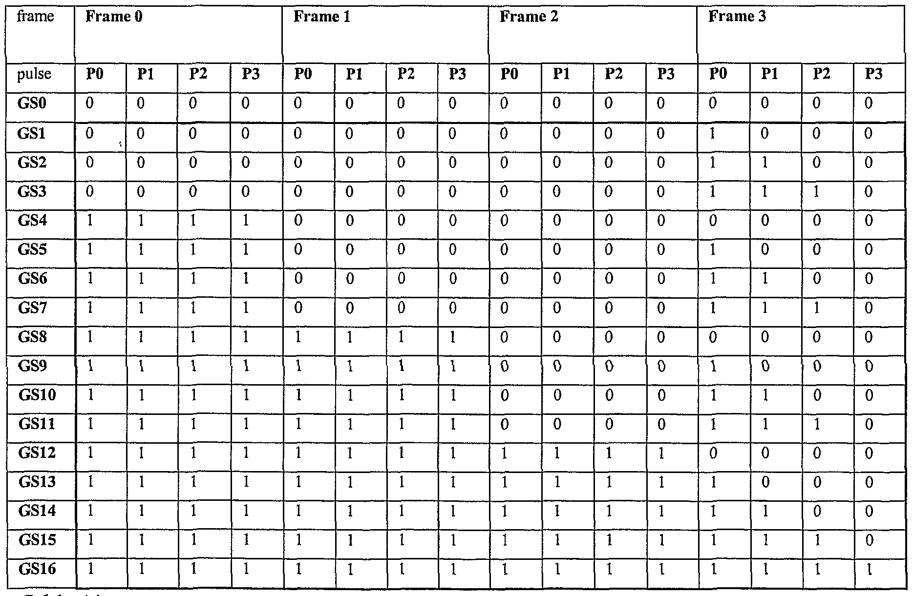
- Table 1 shows a superframe consisting of 4 frames in which 5 gray-levels can be generated.
- GS 3 in e.g. four picture elements (pixels) the driving would be:
- time periods comply with a frame period in which a sequence of time periods is a sequence of frame periods within a sequence of time periods (within a superframe).
- the driving of different picture elements within a sequence of time periods is phase-shifted over one frame period time period relative to each other for different pixels (a phase in this example corresponding to a frame).
- the phase shifting may be altered after each sequence of time periods (superframe).
- FIG. 2 shows a line time split into 4 parts (indicated as sub-line times), which also results in 5 gray levels, while a phase in this example corresponds to a sub-line time.
- the driving of different picture elements within a sequence of time periods is phase-shifted over one frame period time period within two sequential superframes again (a phase now corresponding to a sub-line time).
- the phase shifting is altered after each sequence of time periods (superframe), which implies for example the following driving in the next superframe (Table 5)
- a grayscale-table is defined which is used in driving the display device.
- Each picture element in the matrix (132 rows, 132 columns) has a particular phase (frame number, which is indicated per picture element) which corresponds to a particular frame by which the picture element is driven.
- the phases are repeated in blocks of 2 rows and 4 columns (2 4 mixing).
- the same frame drives each picture element in successive superframes, comparable to the driving shown in Table 2 (see Table 7).
- GS 7 and GS 9 are defined according to Table 9.
- Fp defines a frame (part) (which may be a frame as part of a superframe, like in Tables 2,3 or a phase as part of a frame, like in Tables 4, 5).
- the T represents an on frame (part), a zero corresponds to an off frame (part)
- the picture elements are in the on (black) and off (white) state respectively as indicated in Figure 4.
- a picture element 8(1) displaying gray-level GS 7 is in the on state during phase 0 (FpOoo) of frame 0 (frame (part) 0).
- the notation FpX y y is used in which x refers to the frame, while yy refers to the phase.
- picture elements 8 (2, 3, 4) displaying gray-level GS 7 are driven during the other phases (5, 13, 11 or Fp0 05 , Fp0 ⁇ , FpOn) of frame 0 (frame (part)s 5, 13, 11) in the off state.
- picture elements 8 (5, 6, 7) displaying gray-level GS 7 are driven in the on state during phases 4, 10, 2 or FpOo , FpOio, FpOo 2 of frame 0 (frame (part) 0).
- the picture elements 8 (8) displaying gray-level GS 7 are driven in the off state by phase 7(Fp0 0 ) of frame 0 (frame (part) 7).
- gray-level GS 9 picture elements 8 (10, 11, 13, 14, 15, 16) displaying gray-level GS 9 are driven in the on state during phases 5, 13, 4, 10, 2 and 7 or Fp0 O5 , FpOn, Fp0 04 , Fp0 10 , Fp0 02 and Fp0 07 of frame 0 (frame (part)s 5, 13 , 4, 10, 2, 7 ) and picture elements 8 (9, 12) are driven in the off state by phases 0, 11 or Fp0 00 , FpOi i of frame 0 (frame (part)s 0, 11).
- phase-numbers (frame (part)numbers) are increased by one.
- the picture element 8(1) displaying gray-level GS 7 is in the off state during phase 0 (Fploo) of frame 1 (frame (part) 1).
- Other picture elements 8 (2, 3, 4) displaying gray-level GS 7 are driven in the on state during the other phases (6, 14, 12) or Fplo ⁇ , Fpl ⁇ 4 , Fpl ⁇ 2 of frame 1 (frame (part)s 6, 14, 12).
- picture elements 8 (5, 6, 7) displaying gray-level GS 7 are driven in the off state during phases 5, 11 , 3 or Fplos, Fpl 11 , Fpl ⁇ 3 of frame 1 (frame (part) 1).
- the picture elements 8 (8) displaying gray-level GS 7 are driven in the off state by phase 8 (Fplo 8 ) of frame 1 (frame (part) 8), see Figure 4.
- gray-level GS 9 picture elements 8 (10, 11, 14, 15, 16) displaying gray-level GS 9 are driven in the off state during phases 6, 14, 11, 3 and 8 or Fplo ⁇ .
- Fplu, Fpl a, Fpl 03 and Fplos of frame 1 (frame (part)s 6, 14, 11, 3, 8) and picture elements 8 (9, 12, 13) are driven in the on state by phases 1, 12 and 5 or Fploi, Fpl] 2 , Fplos of frame 1 (frame (part)s 1, 12, 5) , see Figure 4.
- the grayscale (levels) By defining the grayscale (levels) according to Table 9, on and off frames are spread over the superframe as much as possible. As a result, the effective voltage (or root mean square Voltage V- ms ) which the liquid crystal layer encounters is spread evenly over the superframe, thereby suppressing flicker and enabling low frame frequencies. Since adjacent picture elements having substantially the same gray levels are addressed out of phase, the invention enables lowering of the frame frequency. For picture elements addressed in phase (prior art), flicker is visible at a certain frequency, whereas at this same frame frequency flicker is not visible if picture elements are addressed out of phase.
- Figure 5 shows a display device in which multiple row addressing is applied as described in an article by T .
- all rows are driven throughout the frame period with mutually orthogonal signals, for example, Walsh functions.
- each picture element is continuously excited by pulses (in an STN LCD of 240 rows: 256 times per frame period) instead of once per frame period.
- multiple row addressing a (sub-)group ofp rows is driven with mutually orthogonal signals.
- a set of orthogonal signals such as Walsh functions, consists of a plurality of functions which is a power of 2, i.e. 2 s
- the orthogonal row signals Ft(t) are preferably square- wave shaped and consist of voltages +F and -F, while the row voltage is equal to zero outside the selection period.
- the elementary voltage pulses from which the orthogonal signals are built up are regularly distributed across the frame period. In this way, the picture elements are then excited 2 s (or (2 s - 1)) times per frame period with regular intermissions instead of once per frame period.
- the display device of Figure 5 comprises again a matrix 11 of picture elements at the area of crossings of m rows 12 and n columns 13 which are provided as row and column electrodes on facing surfaces of substrates 14, 15, as can be seen in the cross- section shown in the matrix 11.
- the liquid crystal material 16 is present between the substrates.
- Other elements such as orientation layers, polarizers, etc. are omitted in the cross- section for the sake of simplicity.
- the device further comprises a row function generator 17 in the form of, for example, a ROM for generating orthogonal signals F t (t) for driving the rows 12.
- a row function generator 17 in the form of, for example, a ROM for generating orthogonal signals F t (t) for driving the rows 12.
- row vectors driving a group ofp rows via drive circuits 4 are defined during each elementary time interval. The row vectors are written into a row function register 19.
- Information 10 to be displayed is stored in an nxm buffer memory 11 which contains a look-up table 20, for example derived as discussed above with respect to Figure 3 (combination of the Tables 8,9) and read as information vectors per elementary unit of time.
- Signals for the column electrodes 6 are obtained by multiplying the then valid values of the row vector and the information vector during each elementary unit of time and by subsequently adding the obtained products.
- the multiplication of the values of the row and column vectors which are valid during an elementary unit of time is realized by comparing them in an array 22 of m exclusive ORs.
- the addition of the products is effected by applying the outputs of the array of exclusive ORs to the summing logic 13.
- the signals 21 from the summing logic 13 drive a column drive circuit 5 which provides the columns 3 with voltages G j (t) having p+1 possible voltage levels. Every time, ? rows are driven simultaneously, in where p ⁇ N ("multiple row addressing"). As well as the information vectors, the row vectors therefore only havep elements, which results in a saving of the required hardware such as the number of exclusive ORs and the size of the summing circuit, as compared to the method in which all rows are driven simultaneously with mutually orthogonal signals ("Active Addressing").
- the drive electronics is minimized by choosing p to be low, for example, in the range between 3 and 8. Fig.
- F t (t) a set of orthogonal functions
- gray levels can be displayed using this set of orthogonal functions according to the grayscale definition of Table 10.
- GS 6 is defined as having all 4 sub-line times in the on state for frame
- the picture element is in the on state for the first 3 sub-line times, and the 4 th sub-line time the picture element is in the off state, i.e. d 2 ⁇ is -1 for the first 3 sub-line times and +1 for the 4 th line time.
- the picture element is in the on state for all four sub-line times, while for GS 0 the picture element is in the off state for all four sub-line times.
- Function F ⁇ (t) is -1 for the first line time (i.e. 4 sub-line times), +1 for the 2 nd , 3 rd and 4 th line time.
- Function F 2 (t) is -1 for the second line time (i.e. 4 sub-line times), +1 for the first , 3 rd and 4 th line time, etcetera.
- the invention is of course not limited to the embodiments shown.
- the logic in the driver IC can make multiple selections from the programmed orthogonal matrices during frames and also after whole frames. Also vectors within an orthogonal matrix can be swapped or inverted by the driver to reduce the number of column signal transitions.
- the principle of the invention can also be applied to Active matrix LCDs by using time averaging between two gray- values, e.g. averaging over 4 (or 8 or even 16) phases (frames) to reduce the number of generated voltages via the resistor chain.
- Table 13 indicates possible combinations of the standard gray- value generation technique with that of phase-mixing (frame rate control, FRC).
- FRC frame rate control
- Table 14 This can be done for intermediate values between two gray - value GS out of the grayscale of 64 gray -values and as a result 256 gray - values (per color) are obtained which is comparable to using 8 bits in the standard way.
- the advantage is that only 64 buffers are needed in the output stage instead of 256 for the standard way of gray-scale generation. Hence, the source output stage is reduced with 25%, which will result in a significant driver cost reduction.
- phase mixing is applied in a similar way as described above for passive displays.
- the display area is divided into a number of sections. These sections display the contents of different frames, i.e. one section displays frame 1, another sections displays frame 3 etc. In the next frame, these sections display frame 2 and 4 respectively. After 4 frames, each section has displayed all 4 frame contents so that the perceived gray-value is equal for all sections. The smaller the sections the less sensitive is the human eye for flicker artifacts. As an example, Tables 15 and 16 show the generation of gray- value 18.25 for the total display area in time.
- the display is e.g. divided into 8 sections. In these sections the phase (frame number) is indicated.
- the definition table (of Table 14 in this case)) shows which content to display at each phase (frame) number. After each phase (frame), the phase (frame) number is increased by one. In this example, the entire display area will show gray- value 18.25 as defined in table 15.
- the sections are in different phases (different frame numbers). This phase shift makes the flicker artifact less visible for the human eye. As a consequence, the frame frequency at which the flickering becomes visible is reduced due to the frame mixing. As a result, the power consumption is reduced further.
Abstract
Description


Claims
Priority Applications (5)
| Application Number | Priority Date | Filing Date | Title |
|---|---|---|---|
| US10/535,369 US20060082559A1 (en) | 2002-11-21 | 2003-10-28 | Display device |
| JP2004552956A JP2006507523A (en) | 2002-11-21 | 2003-10-28 | Display device |
| CN200380103754XA CN1726527B (en) | 2002-11-21 | 2003-10-28 | Liquid crystal display device |
| AU2003274495A AU2003274495A1 (en) | 2002-11-21 | 2003-10-28 | Liquid crystal display device |
| EP03758470A EP1565904A2 (en) | 2002-11-21 | 2003-10-28 | Display device |
Applications Claiming Priority (2)
| Application Number | Priority Date | Filing Date | Title |
|---|---|---|---|
| EP02079852.6 | 2002-11-21 | ||
| EP02079852 | 2002-11-21 |
Publications (2)
| Publication Number | Publication Date |
|---|---|
| WO2004047066A2 true WO2004047066A2 (en) | 2004-06-03 |
| WO2004047066A3 WO2004047066A3 (en) | 2004-08-19 |
Family
ID=32319639
Family Applications (1)
| Application Number | Title | Priority Date | Filing Date |
|---|---|---|---|
| PCT/IB2003/004829 WO2004047066A2 (en) | 2002-11-21 | 2003-10-28 | Liquid crystal display device |
Country Status (8)
| Country | Link |
|---|---|
| US (1) | US20060082559A1 (en) |
| EP (1) | EP1565904A2 (en) |
| JP (1) | JP2006507523A (en) |
| KR (1) | KR100982083B1 (en) |
| CN (1) | CN1726527B (en) |
| AU (1) | AU2003274495A1 (en) |
| TW (1) | TWM253785U (en) |
| WO (1) | WO2004047066A2 (en) |
Families Citing this family (4)
| Publication number | Priority date | Publication date | Assignee | Title |
|---|---|---|---|---|
| US8885139B2 (en) * | 2005-01-21 | 2014-11-11 | Johnson & Johnson Vision Care | Adaptive electro-active lens with variable focal length |
| KR101313007B1 (en) * | 2006-06-12 | 2013-10-01 | 존슨 앤드 존슨 비젼 케어, 인코포레이티드 | Method to reduce power consumption with electro-optic lenses |
| GB0623769D0 (en) * | 2006-11-28 | 2007-01-10 | Seos Ltd | Method and apparatus for reducing motion blur in a displayed image |
| US8098333B2 (en) * | 2007-06-29 | 2012-01-17 | Seiko Epson Corporation | Phase shift insertion method for reducing motion artifacts on hold-type displays |
Citations (6)
| Publication number | Priority date | Publication date | Assignee | Title |
|---|---|---|---|---|
| EP0364307A2 (en) * | 1988-10-14 | 1990-04-18 | Compaq Computer Corporation | Method and apparatus for displaying different shades of gray on a liquid crystal display |
| US5337408A (en) * | 1991-08-09 | 1994-08-09 | Vadem Corporation | Multi-level display controller |
| US5400044A (en) * | 1990-06-29 | 1995-03-21 | Acorn Computers Limited | Method and apparatus for producing grey levels on a raster scan video display device |
| US5479188A (en) * | 1993-06-02 | 1995-12-26 | Nec Corporation | Method for driving liquid crystal display panel, with reduced flicker and with no sticking |
| US5565883A (en) * | 1992-02-05 | 1996-10-15 | Nec Corporation | Active matrix liquid crystal display unit capable of suppressing flicker and cross talk |
| US5774101A (en) * | 1994-12-16 | 1998-06-30 | Asahi Glass Company Ltd. | Multiple line simultaneous selection method for a simple matrix LCD which uses temporal and spatial modulation to produce gray scale with reduced crosstalk and flicker |
Family Cites Families (14)
| Publication number | Priority date | Publication date | Assignee | Title |
|---|---|---|---|---|
| JPH02285391A (en) * | 1989-04-26 | 1990-11-22 | Hosiden Corp | Multi-level display method for active matrix liquid crystal cell |
| JP3137367B2 (en) * | 1990-08-09 | 2001-02-19 | 株式会社東芝 | Color panel display control system and computer system |
| US5337804A (en) * | 1993-05-06 | 1994-08-16 | Belle De St. Claire | Adjustable mold positioner |
| JP3582919B2 (en) * | 1994-12-16 | 2004-10-27 | 旭硝子株式会社 | Driving method of image display device |
| JPH08227283A (en) * | 1995-02-21 | 1996-09-03 | Seiko Epson Corp | Liquid crystal display device, its driving method and display system |
| US5751264A (en) * | 1995-06-27 | 1998-05-12 | Philips Electronics North America Corporation | Distributed duty-cycle operation of digital light-modulators |
| JPH10161610A (en) * | 1996-12-05 | 1998-06-19 | Hitachi Ltd | Liquid crystal display unit |
| JPH1124637A (en) * | 1997-07-04 | 1999-01-29 | Optrex Corp | Drive method for simple matrix liquid crystal display |
| JP3767127B2 (en) * | 1997-10-24 | 2006-04-19 | セイコーエプソン株式会社 | Liquid crystal display panel driving device, liquid crystal display device, and electronic apparatus |
| US6008794A (en) * | 1998-02-10 | 1999-12-28 | S3 Incorporated | Flat-panel display controller with improved dithering and frame rate control |
| US6198469B1 (en) * | 1998-07-01 | 2001-03-06 | Ignatius B. Tjandrasuwita | “Frame-rate modulation method and apparatus to generate flexible grayscale shading for super twisted nematic displays using stored brightness-level waveforms” |
| JP3094014B2 (en) * | 1999-02-09 | 2000-10-03 | 株式会社ナナオ | Image display method and image display device |
| WO2002017006A2 (en) * | 2000-08-23 | 2002-02-28 | Dejima Tech B.V. | Single-polarizer, normally white reflective stn display |
| TW544650B (en) * | 2000-12-27 | 2003-08-01 | Matsushita Electric Ind Co Ltd | Matrix-type display device and driving method thereof |
-
2003
- 2003-10-28 KR KR1020057009114A patent/KR100982083B1/en not_active IP Right Cessation
- 2003-10-28 EP EP03758470A patent/EP1565904A2/en not_active Withdrawn
- 2003-10-28 WO PCT/IB2003/004829 patent/WO2004047066A2/en active Application Filing
- 2003-10-28 US US10/535,369 patent/US20060082559A1/en not_active Abandoned
- 2003-10-28 CN CN200380103754XA patent/CN1726527B/en not_active Expired - Fee Related
- 2003-10-28 AU AU2003274495A patent/AU2003274495A1/en not_active Abandoned
- 2003-10-28 JP JP2004552956A patent/JP2006507523A/en active Pending
- 2003-11-18 TW TW092220378U patent/TWM253785U/en not_active IP Right Cessation
Patent Citations (6)
| Publication number | Priority date | Publication date | Assignee | Title |
|---|---|---|---|---|
| EP0364307A2 (en) * | 1988-10-14 | 1990-04-18 | Compaq Computer Corporation | Method and apparatus for displaying different shades of gray on a liquid crystal display |
| US5400044A (en) * | 1990-06-29 | 1995-03-21 | Acorn Computers Limited | Method and apparatus for producing grey levels on a raster scan video display device |
| US5337408A (en) * | 1991-08-09 | 1994-08-09 | Vadem Corporation | Multi-level display controller |
| US5565883A (en) * | 1992-02-05 | 1996-10-15 | Nec Corporation | Active matrix liquid crystal display unit capable of suppressing flicker and cross talk |
| US5479188A (en) * | 1993-06-02 | 1995-12-26 | Nec Corporation | Method for driving liquid crystal display panel, with reduced flicker and with no sticking |
| US5774101A (en) * | 1994-12-16 | 1998-06-30 | Asahi Glass Company Ltd. | Multiple line simultaneous selection method for a simple matrix LCD which uses temporal and spatial modulation to produce gray scale with reduced crosstalk and flicker |
Non-Patent Citations (2)
| Title |
|---|
| OHISHI I ET AL: "AN EVALUATION OF FLICKER ON SPACE MODULATED FRAME RATE CONTROL MULTI-GRAY SHADING METHODS FOR STN-LCDS" IEICE TRANSACTIONS ON ELECTRONICS, INSTITUTE OF ELECTRONICS INFORMATION AND COMM. ENG. TOKYO, JP, vol. E79-C, no. 8, 1 August 1996 (1996-08-01), pages 1063-1068, XP000632424 ISSN: 0916-8524 * |
| SASAKI I ET AL: "MAGIC-SQUEARE-METHOD FRAME-RATE-CONTROL TECHNOLOGY" SID INTERNATIONAL SYMPOSIUM DIGEST OF TECHNICAL PAPERS. SAN JOSE, JUNE 14 - 16, 1994, SANTA ANA, SID, US, vol. 25, 14 June 1994 (1994-06-14), pages 259-262, XP000462709 * |
Also Published As
| Publication number | Publication date |
|---|---|
| AU2003274495A1 (en) | 2004-06-15 |
| EP1565904A2 (en) | 2005-08-24 |
| AU2003274495A8 (en) | 2004-06-15 |
| US20060082559A1 (en) | 2006-04-20 |
| CN1726527A (en) | 2006-01-25 |
| JP2006507523A (en) | 2006-03-02 |
| KR20050085067A (en) | 2005-08-29 |
| WO2004047066A3 (en) | 2004-08-19 |
| KR100982083B1 (en) | 2010-09-13 |
| CN1726527B (en) | 2010-05-26 |
| TWM253785U (en) | 2004-12-21 |
Similar Documents
| Publication | Publication Date | Title |
|---|---|---|
| KR100234612B1 (en) | Memory interface circuit and access method | |
| KR100965571B1 (en) | Liquid Crystal Display Device and Method of Driving The Same | |
| KR100199257B1 (en) | Device and method for displaying liquid crystal | |
| KR100515468B1 (en) | Method and apparatus for driving passive matrix liquid crystal, method and apparatus for multiline addressing driving of passive matrix liquid crystal, and liquid crystal display panel | |
| JP3606830B2 (en) | Cholesteric LCD driver | |
| JPH09319342A (en) | Liquid crystal display device, and driving method for the device | |
| US8659528B2 (en) | Electro-optical device driven by polarity reversal during each sub-field and electronic apparatus having the same | |
| EP0704087B1 (en) | A method of driving a picture display device | |
| KR20060080933A (en) | A bi-stable display with reduced memory requirement | |
| US6597335B2 (en) | Liquid crystal display device and method for driving the same | |
| US20060109226A1 (en) | Relative brightness adjustment for LCD driver ICs | |
| WO2004047066A2 (en) | Liquid crystal display device | |
| JP4017425B2 (en) | Simple matrix liquid crystal driving method and liquid crystal driving device | |
| KR100542686B1 (en) | Apparatus of multi gray scale display using pulse width modulation | |
| JP2003005695A (en) | Display device and multi-gradation display method | |
| JP3791997B2 (en) | Driving method of liquid crystal display device | |
| JP2002149119A (en) | Method and circuit for driving liquid crystal display device | |
| JP2006235417A (en) | Liquid crystal display apparatus | |
| JP3576231B2 (en) | Driving method of image display device | |
| JP3591926B2 (en) | Driving method of liquid crystal display | |
| JP2004093666A (en) | Liquid crystal driving device and liquid crystal driving method | |
| KR100322447B1 (en) | A liquid crystal display using mixing grace scale | |
| JP3979827B2 (en) | Multi-line addressing driving method and apparatus for simple matrix liquid crystal | |
| JPH1049108A (en) | Gradation display method for liquid crystal device | |
| JP3630185B2 (en) | Driving method of liquid crystal panel |
Legal Events
| Date | Code | Title | Description |
|---|---|---|---|
| AK | Designated states |
Kind code of ref document: A2 Designated state(s): AE AG AL AM AT AU AZ BA BB BG BR BY BZ CA CH CN CO CR CU CZ DE DK DM DZ EC EE EG ES FI GB GD GE GH GM HR HU ID IL IN IS JP KE KG KP KR KZ LC LK LR LS LT LU LV MA MD MG MK MN MW MX MZ NI NO NZ OM PG PH PL PT RO RU SC SD SE SG SK SL SY TJ TM TN TR TT TZ UA UG US UZ VC VN YU ZA ZM ZW |
|
| AL | Designated countries for regional patents |
Kind code of ref document: A2 Designated state(s): GH GM KE LS MW MZ SD SL SZ TZ UG ZM ZW AM AZ BY KG KZ MD RU TJ TM AT BE BG CH CY CZ DE DK EE ES FI FR GB GR HU IE IT LU MC NL PT RO SE SI SK TR BF BJ CF CG CI CM GA GN GQ GW ML MR NE SN TD TG |
|
| 121 | Ep: the epo has been informed by wipo that ep was designated in this application | ||
| WWE | Wipo information: entry into national phase |
Ref document number: 2003758470 Country of ref document: EP |
|
| ENP | Entry into the national phase |
Ref document number: 2006082559 Country of ref document: US Kind code of ref document: A1 |
|
| WWE | Wipo information: entry into national phase |
Ref document number: 10535369 Country of ref document: US |
|
| WWE | Wipo information: entry into national phase |
Ref document number: 2004552956 Country of ref document: JP |
|
| WWE | Wipo information: entry into national phase |
Ref document number: 1020057009114 Country of ref document: KR Ref document number: 20038A3754X Country of ref document: CN |
|
| WWP | Wipo information: published in national office |
Ref document number: 2003758470 Country of ref document: EP |
|
| WWP | Wipo information: published in national office |
Ref document number: 1020057009114 Country of ref document: KR |
|
| WWP | Wipo information: published in national office |
Ref document number: 10535369 Country of ref document: US |