A MICROFLUIDIC DESIGN AUTOMATION METHOD AND SYSTEM
CROSS-REFERENCES TO RELATED APPLICATIONS
, This application claims priority from U.S. Provisional Patent Application No. 60/214,595, titled "Biological Design Automation System," by Michael Lee, et. al., filed June 27, 2000.
BACKGROUND OF THE INVENTION
The present invention generally relates to microfluidics and more particularly to the design of customized microfluidic systems using a microfluidic computer aided design system. Such customized microfluidic systems may be used, for example, for fluid analysis of biological samples.
Typically microfluidic systems for processing fluid samples employ a series of chambers each configured for subjecting the fluid sample to a specific processing step. As the fluid sample flows through the system sequentially from chamber to chamber, the fluid sample undergoes the processing steps according to a specific protocol. Because different protocols require different configurations, the design and manufacturing of such microfluidic systems can be time-consuming and costly.
Conventional computer aided design tools such as AutoCAD® are inadequate for the design and layout of microfluidic systems. For instance, AutoCAD® is a general tool, and has no drawing constraints and provides no specific microfluidic design information associated with a component.
Thus there is a need for computerized design techniques which allow the quick and easy formation of microfluidic systems with different configurations and utilizing different protocols.
SUMMARY OF THE INVENTION
The present invention provides for the design of a microfluidic system, including a microfluidic chip or circuit, using an object oriented microfluidic computer aided design (CAD) system. The microfluidic CAD system, henceforth referred to as the "MCAD" system, provides the user with the tools to design, analyze, and implement a customized
microfluidic system using a plurality of building block microfluidic components. The MCAD system overcomes the disadvantages of conventional CAD tools by providing, for instance, drawing constraints, design information associated with components, I/O ports, and connectivity to I/O ports, as well as easy layout and manipulation of multilayered components.
In one embodiment the microfluidic system may include a network of single or multi-layer elastomeric structures, hi an alternate embodiment some or all the structures may include rigid materials (e.g., silicon-based materials). In yet another embodiment some of the structures may include a mixture of flexible materials, (e.g., elastomeric materials) with the rigid material. Utilization of such an MCAD system can lead to quick and easy implementation of simple to highly complex networks for use in general microfluidic transfer control systems, biological diagnostics systems, etc.
In one embodiment of the present invention a microfluidic device or chip is created from a plurality of microfluidic components according to a design. First a template is selected. Next, the components are placed on the template, manually or automatically, using a placement tool. The components include multilayered components. The components are then routed, manually or automatically, using a routing tool based on preset design rule constraints to achieve a physical layout. Functional analysis (e.g., logical microfluidic flow simulation) and/or physical analysis, (e.g., dynamic microfluidic flow simulation) may then be performed on the physical layout. Following the optional functional analysis and/or physical analysis, the physical layout is used to create the chip layout file, which is later used for fabricating the microfluidic device or chip. In one embodiment of the present invention a microfluidic circuit design method is provided. The method includes developing synthesizable computer code for a design. Next, a microfluidic circuit schematic, including a plurality of symbols for microfluidic components, is generated either interactively or using the synthesizable computer code. A symbol may include at least one control channel and at least one fluid channel. The microfluidic circuit schematic is then functionally simulated. The microfluidic components are placed and routed on a template to form a physical layout. Then the physical layout is physically simulated using dynamic simulation models of the microfluidic components; and the physical layout is written to a layout file.
In one embodiment of the present invention a microfluidic device or chip is created from a plurality of microfluidic components according to a design. First a template is selected. Next, the components are placed on the template, manually or automatically, using a placement tool. The components include multilayered components. The components are
then routed, manually or automatically, using a routing tool based on preset design rule constraints to achieve a physical layout. Functional analysis (e.g., logical microfluidic flow simulation) and/or physical analysis, (e.g., dynamic microfluidic flow simulation) may then be performed on the physical layout. Following the optional functional analysis and/or physical analysis, the physical layout is used to create the chip layout file, which is later used for fabricating the microfluidic device or chip.
In one embodiment of the present invention a microfluidic circuit design system is provided. The system includes: a synthesis module for synthesizing software of a design into a component level description of the design. The design has a plurality of microfluidic components, and the component level description has symbols associated with the plurality of microfluidic components. The system further includes a design capture module, including a schematic entry tool, for placing and connecting the symbols on a schematic according to the design; and a functional analysis module for functionally simulating selected symbols of the schematic. In another embodiment of the present invention a method, using a computer system, for designing a microfluidic circuit schematic including a plurality of microfluidic component symbols associated with a plurality of microfluidic components is provided. The method includes: placing a first component symbol of the plurality of microfluidic component symbols on a schematic; placing a second component symbol of the plurality of microfluidic component symbols on the schematic; and connecting the first component symbol to the second component symbol.
In another embodiment of the present invention a method for capturing a design of a microfluidic system using a computer aided design tool is provided. A first symbol representing a first component of a plurality of microfluidic components is placed on a schematic, where the first component includes a first fluid channel and a first control channel. Next a second symbol representing a second component of the plurality of microfluidic components, is placed on the schematic, where the second component includes a second fluid channel and a second control channel. Then the first symbol is connected to the second symbol. An alternative embodiment of the present invention discloses a design capture system for capturing a microfluidic circuit including a plurality of microfluidic components. The design capture system includes: a component library including information and symbols associated with the plurality of microfluidic components; and a schematic entry module used for placing and connecting the symbols.
Another embodiment of the present invention discloses a method for synthesizing a network model of a microfluidic circuit including a plurality of microfluidic components. First, a synthesis program is stored in a computer readable medium. Next component models associated with the plurality of microfluidic components are selected from a database. And using the component models and the synthesis program, the network model is generated. Where in the network model, the component models are connected together. In yet another embodiment of the present invention a synthesis system for creating a schematic of a microfluidic circuit having a plurality of microfluidic components, is provided. The synthesis system includes: a memory for storing synthesis code related to the schematic; a design library having a plurality of indications associated with the plurality of microfluidic components, wherein selected indications are selected using the synthesis code; and a synthesis module for creating the schematic by connecting the selected indications.
An embodiment of the present invention provides a method for functionally analyzing a schematic of a microfluidic circuit including a plurality of microfluidic components. The method includes: selecting a functional model for a component of the plurality of microfluidic components; determining a logic control test sequence for the schematic; and using the functional model in the schematic and the logic control test sequence, functionally simulating the schematic. Another embodiment of the present invention provides a microfluidic circuit design system including one or more of the following: a synthesis module for synthesizing software of a design into a schematic having a plurality of connected symbols of microfluidic components; a design capture module for displaying and manipulating the schematic; a functional analysis module for functionally simulating selected microfluidic components of the schematic; a physical implementation module for placing and routing the microfluidic components into a physical layout according to the design; and a physical analysis module for physically simulating the components in the physical layout.
Another embodiment of the present invention is directed to a method, using a physical layout system, for laying out a microfluidic circuit including a plurality of microfluidic components, where the microfluidic components include multilayered components. The method includes: placing a first component of the plurahty of microfluidic components; placing a second component of the plurality of microfluidic components; and connecting the first component to the second component.
In another embodiment of the present invention a method is provided, using a computer system, for physically laying out a microfluidic circuit including a plurality of microfluidic components. The method includes: selecting a template; placing a first microfluidic component with an associated property, such as physical scaling, physical property, layer assignment, equations of motion, simulation data, macro logic functions, or functional definition, on the template; placing a second microfluidic component on the template; and connecting the first component to the second component. The connecting may include a design rule check.
In yet another embodiment of the present invention a microfluidic circuit physical layout method, using a computer, is provided. The method includes: selecting a template including an I/O port; placing a microfluidic component on the template, wherein the microfluidic component has a component control channel and a component fluid channel; and connecting the component control channel to the I/O port.
Another embodiment of the present invention includes a method for physical layout of a microfluidic system using a computer aided design tool. The microfluidic system includes a plurality of microfluidic components. First, a template is selected, including a plurality of layers. Next, a first symbol representing a first component of the plurality of microfluidic components is placed. The first symbol includes a first fluid channel symbol and a first control channel symbol. The first control channel symbol and the first fluid channel symbol are on different layers. Next, a second symbol representing a second component of the plurahty of microfluidic components is placed. The second symbol includes a second fluid channel symbol. The first fluid channel symbol is connected or routed to the second fluid channel symbol.
An embodiment of the present invention provides a method for validating a physical layout of a microfluidic circuit design including a plurality of microfluidic components, the method includes placing and routing the plurality of microfluidic components on a template to form the physical layout of the microfluidic circuit design. Next, a dynamic simulation model is determined for each component of the plurality of microfluidic components on the template. Using the physical layout and dynamic simulation models for the plurality of microfluidic components, the physical layout is physically simulated.
An embodiment of the present invention provides a method for device implementation of a microfluidic circuit including a plurality of microfluidic components. The method includes placing and routing the plurality of microfluidic components on a
template to form a physical layout of the microfluidic circuit design. Then the physical layout is written to a layout file to be used for manufacturing. Next, a mask is created for a die of a plurality of dies using the layout file, where the die includes the physical layout. The plurality of dies on a wafer are laid out, where the mask creates the die on the wafer. An embodiment of the present invention provides, in a computer system having a computer memory and an object-oriented environment, a method for providing a microfluidic component of a microfluidic circuit. First, a first symbol layer object having a first child channel object is invoked. Next, a second symbol layer object having a second child object is invoked. And then a microfluidic component symbol representing the microfluidic component, is formed. The microfluidic component symbol includes the first child channel object and the second child channel object.
In another embodiment of the present invention, in a computer system having a computer memory and an object-oriented environment, a method for physically laying out a microfluidic circuit, having a plurality of microfluidic components is provided. First, a first symbol object representing a microfluidic component is placed, where the first symbol object includes a fluid channel object which represents a first fluid channel of the microfluidic component. Next, a connecting fluid channel object on a channel layer is placed, where the connecting fluid channel object represents a second fluid channel used to connect two microfluidic components of the plurality of microfluidic components. The fluid channel object is then linked to the connecting fluid channel object, where the linking represents connecting the first fluid channel to the second fluid channel.
Another embodiment of the present invention provides a object-oriented system for laying out a microfluidic circuit having a plurality of microfluidic components, on a template having a plurality of layers. The system includes: a model object representing the laid out microfluidic circuit on the template; a symbol object associated with a microfluidic component of the plurality of microfluidic components the symbol object being part of the model object; a plurality of symbol layer objects associated with a fluid layer and a control layer of the microfluidic component, the plurality of symbol layer objects being part of the symbol object; a component fluid channel object associated with the fluid layer of the microfluidic component, the component fluid channel object being part of a symbol layer object of the plurality of symbol layer objects; a layer object associated with a fluid layer of the plurality of layers, the layer object being part of the model object; a fluid channel object associated with a fluid channel on the fluid layer of the plurality of layers, the fluid channel object being part of the layer object; and a linking model for linking the component fluid
channel object with the fluid channel object, when the microfluidic component is connected to the fluid channel on the template.
In yet another embodiment of the present invention an object- oriented system stored in a computer readable memory is provided, the system includes a model class object for providing a container for objects on a drawing area. The model class object owns, a symbol object and a primary layer object, where the symbol object provides a representation of a microfluidic component and the primary layer object provides a layer for the drawing area. In addition the object- oriented system may further include, the symbol object owning a symbol layer object, where the symbol layer object for provides a layer for the microfluidic component. The symbol layer object owns a first child channel object, where the first child channel object provides a channel for forming microfluidic component. The first child channel object owns a component port object. Also, the primary layer owns a child channel layer object, where the channel layer object provides an intermediate layer for a connecting channel on the drawing area. The channel layer object owns a second channel object which in turn owns a channel port. The channel port object is linked to the component port object for providing a connection between the channel of the microfluidic component and the connecting channel;
An advantage of the present invention is the reduction in time needed to complete the design and implementation of a microfluidic circuit. For example, in one embodiment of the present invention, synthesis, schematic capture, and functional simulation allow an efficient and expedient process of creating and validating an initial design, the physical layout tool allows easy placement and routing of multilayered components on a predefined template, the physical simulation allows the reduction in errors before fabrication, and the die placement tool allows faster wafer mask generation. The uses and results generated by the present invention include cell based assays (including micro cell sorting, genomic analysis, such as DNA sizing, hybridization, sequencing, quantification, and amplification); protein analysis, crystallization and purification; MS-interface; biochemical and electrophysiological assays, gene expressions; differential display analysis; integrated biological sample preparation; single molecule analysis; drug delivery; diagnostics; and other uses and products related to the chemical, biochemical, biological, electronic, computer, appliance, pharmaceutical, medical, or power industries.
These and other embodiments of the present invention are described in more detail in conjunction with the text below and attached figures.
BRIEF DESCRIPTION OF THE DRAWINGS
FIG. 1 shows a simplified block diagram of the MCAD system of an embodiment of the present invention ;
FIG. 2A is a simplified cross-sectional view of microfluidic switch along channel of an embodiment of the present invention;
FIG. 2B is a simplified cross-sectional view of microfluidic switch along channel of an embodiment of the present invention;
FIG. 3 is a simplified top down view of microfluidic switch of an embodiment of the present invention FIGS. 4A-4K show symbols representing microfluidic devices of an embodiment of the present invention;
FIGS. 5A and 5B show an example of a microfluidic NAND gate of an embodiment of the present invention;
FIGS. 6A ands 6B show an example of a microfluidic S-R latch of an embodiment of the present invention;
FIG. 7A shows a symbol for a D-latch of an embodiment of the present invention;
FIG. 7B shows the gates synthesized from the above VHDL code example of an embodiment of the present invention FIG. 8 shows a simplified block diagram of phase 2, design capture, of an embodiment of the present invention;
FIGS. 9a and 9b show simplified top plan view and perspective view of an on- off valve component of an embodiment of the present invention;
FIG. 10 shows an IDEFO diagram representing a microfluidic component of an embodiment of the present invention;
FIG. 11 shows a microfluidic valve symbol of an embodiment of the present invention;
FIG. 12 illustrates a schematic capture display window of embodiment of the present invention; FIG. 13 A shows an example of a peristaltic pump connected to a T-switch in an expanded drawing area of FIG. 12 of an embodiment of the present invention;
FIG. 13B shows an example of using IDEFO blocks to perform schematic capture in another embodiment of the present invention;
FIG. 14 shows a simplified block diagram for the connected component functional models of the functional analysis of the MCAD system of an embodiment of the present invention;
FIG. 15 shows a simplified block diagram of the physical implementation of an embodiment of the present invention;
FIGS. 16A and 16B give examples of pre-defined templates of an embodiment of the present invention;
FIG. 17A shows the physical dimensions for an interconnect bridge channel of an embodiment of the present invention; FIG. 17B shows a symbol for an interconnect bridge of one embodiment of the present invention;
FIG. 18A shows a simplified view of a crossing of two channels located on the same layer;
FIG. 18B shows a simplified view of an interconnect bridge channel using vias of an embodiment to of the present invention;
FIG. 19 shows a physical layout tool of one embodiment of the present invention;
FIG. 20 shows a symbol for a microfluidic valve of one embodiment of the present invention; FIG. 21 shows two components of an embodiment of the present invention;
FIG. 22 shows the control channels on the control layer for the two components of FIG. 21;
FIG. 23 shows the fluid channels for the fluid layer for the two components of FIG. 21; FIG. 24 shows a partially connected layout of a microfluidic circuit having a rotary pump and a channel array of an embodiment of the present invention;
FIG. 25 shows a simplified flowchart having the steps involved in the physical layout of a microfluidic circuit of an embodiment of the present invention;
FIG. 26 shows a simplified view of a pressure oscillator structure of one embodiment of the present invention;
FIG. 27 shows a physical layout of a cell sorter of an embodiment of the present invention;
FIG. 28 shows an expanded view of the physical layout of the cell sorter of an embodiment of the present invention;
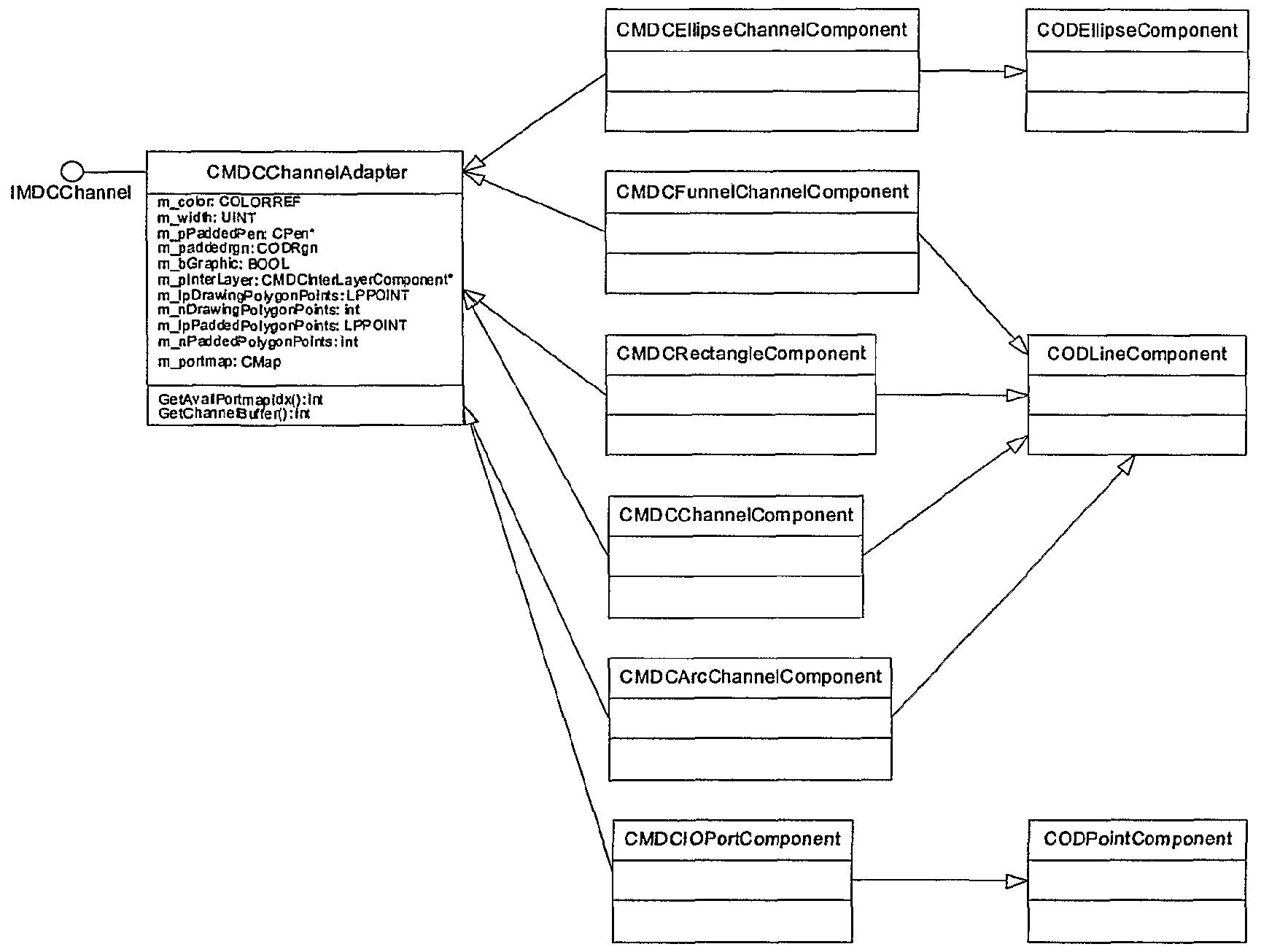
Fig. 28-1 shows a simplified UML diagram of the object relationships of an embodiment of the present invention;
FIG. 29 shows a display for setting up the die layout on a wafer of an embodiment of the present invention; and FIGS. 30-56 show various embodiments of microfluidic devices.
DESCRIPTION OF THE SPECIFIC EMBODIMENTS
Embodiments of the present invention are directed to the design of customized microfluidic systems using a microfluidic computer aided design (MCAD) system. The MCAD system provides the user with the tools to design, analyze, and implement a customized microfluidic system using a plurality of building block microfluidic components. In one embodiment of the invention, the MCAD system includes a design capture module including a schematic entry tool for selecting and connecting microfluidic components according to a design. The system further includes a functional analysis module for functionally simulating selected microfluidic components of the design, a physical implementation module for arranging the microfluidic components into a physical layout according to the design, and a physical analysis module for physically simulating the microfluidic components in the physical layout.
In some embodiments, the modules comprise computer instructions or code stored in a computer-readable medium. The computer-readable medium is operatively coupled to a network (e.g., an internal computer bus, an external Local Area Network (LAN), or the Internet) to permit access to the instructions via the network.
The microfluidic components may be selected from a library or libraries having, for example, channels, pumps, valves, chambers, and layer interconnects (or vias). The library or libraries include normalized, custom, pre-defined, and/or user-defined, microfluidic components. The microfluidic components are connected according to preset design rules. The microfluidic components may be assigned physical scaling and physical properties. The selected components are typically active fluidic components.
The microfluidic components may include conventional microfluidic structures composed of hard, inflexible materials (such as silicon) or microfluidic structures made out of various layers of elastomer bonded together. An embodiment of the present invention uses a multi-layer soft lithography process to build integrated (i.e., monolithic) microfabricated elastomeric structures. Advantages of fabricating the elastomeric structures
by binding together layers of soft elastomeric materials include the fact that the resulting devices are reduced by more than two orders of magnitude in size as compared to silicon- based devices. Further advantages of rapid prototyping, ease of fabrication, and biocompatability are also achieved. Further details may be found in PCT Patent Application No. PCT/USOO/17740, entitled "Microfabricated Elastomeric Valve And Pump Systems," filed June 27, 2000; Hou-Pu Chou et al., "Integrated Elastomer Fluidic Lab-on-a-chip - Surface Patterning and DNA Diagnostics," Proceedings of the Solid State Actuator and Sensor Workshop, Hilton Head, S.C. (2000); Stephen R. Quake and Axel Scherer, "From Micro- to Nanofabrication with Soft Materials," Science 290: 1536-40 (2000); and M. A. Unger et al., "Monolithic Microfabricated Valves and Pumps by Multilayer Soft
Lithography," Science 288: 113-116 (2000). These are incorporated herein by reference each in its entirety.
The selected microfabricated components of the design may be functionally simulated by applying control stimuli to the control channels of selected active fluidic components to show functional connectivity of the design. In one embodiment of the functional simulation, components of the design are represented by Boolean expressions with operands based on connection ports of the control channels of the active fluidic components. Actuation of the active fluidic components is simulated using control stimulus generated by a Boolean based language with timing constraints. The design may be modified based on results of the functional simulation.
The microfluidic components in the physical layout may be physically analyzed. The physical analysis may include, for instance, analyzing dynamic volumetric flow rates in the components, analyzing component volumes, and analyzing volumetric capacitances of interconnecting and routing channels in the physical layout. Physically simulating the components of the physical layout may include simulating actuation of dynamic fluid flow in the components using control stimulus generated by a Boolean based language. The physical layout may be modified based on results of the physical simulation. The physical layout may be written to a layout file to be used for manufacturing.
For the purposes of this application a channel, for example, a control channel or a fluid/fluidic channel, may contain either a gas or a hquid. In one embodiment the control layer has pressurized air and the fluid layer has a liquid substance. Other embodiments have other combinations of gas-gas, liquid-gas, or liquid-liquid in two or more channels.
FIG. 1 shows a simplified block diagram of the MCAD system 10 of an embodiment of the present invention. There are four primary phases (phases 1, 2, 4, and 6)
and two secondary phases (phases 3 and 5). Design conception 100 is the first step (phase 1) where the desired functionality of the microfluidic circuit is determined. Once the functionality has been determined, the second primary step 200 (phase 2) is to capture the resulting circuit schematically using basic predefined components 206, macro components 210, or user-defined components. The components may be microfluidic multilayered structures with at least one control channel and at least one fluid channel, where the control channel controls the fluid (liquid or gas) flow through the fluid channel. These channels may contain either a liquid or a gaseous substance. The third primary step 400 (phase 4) is the physical implementation of the design and involves the physical layout (i.e., placing and routing the components making up the circuit) either manually or automatically, from a two and/or three dimensional perspective. The fourth, and final, primary step 900 (phase 6) is the actual creation of the microfluidic chip. The two optional secondary phases 360 and 800 are shown as well and are used at different points of the MCAD system 10. These secondary phases involve, respectively, the functional analysis and physical analysis of the described design and layout. Functional analysis 360 (phase 3) aides the designer in verifying the desired function or behavior of the design. Examples of functional analysis are connectivity analysis to determine if the components are connected together or control channel analysis to determine that the proper control channels are activated in the right sequence. Physical analysis 800 (phase 5) allows the designer to verify and analyze the dynamic performance of the design. While functional and physical analyses are not critical for simple low component count design, they become important for moderately complex to highly complex designs by minimizing the need to empirically test and redesign until the desired network is achieved. Conception (Phase 1)
The microfluidic circuit or chip design begins with the conception 100 of the desired functionality, outputs, or results to be achieved by inputting fluids into the microfluidic circuit or chip (phase 1).
One specific embodiment employs a black box analysis in which the inputs and outputs are first determined. A computer program using a synthesis language may then be written to simulate the generation of the outputs from the inputs. The synthesis language can be run through a synthesis compiler to generate a microfluidic circuit having a plurality of interconnected microfluidic components or structures. The synthesis compiler may also optimize a part of or all of the microfluidic circuit according to some criteria, such as minimum area. In such an embodiment, the design capture (phase 2) in effect is
automatically done by the synthesis tool with access to the macro library 210 and basic library 206.
A fluidic synthesis language is like a synthesis language in the electrical arts in that certain programming language constructs map to certain structures or combinations of structures. For example, in electronic circuit design, a Hardware Description Language
(HDL), such as VHSIC HDL (VHDL) or Verilog, is used to simulate the behavior of a circuit design at an abstract level (e.g., at the Register Transfer Language (RTL) level). Then, the VHDL or Verilog code is used by a synthesis tool (e.g., a tool available from Synopsys Inc. of Mountain View, California) to produce an optimized gate level description of the circuit. As a simple illustration the operators in Boolean logic, such as "not," "and," or "or," map to an inverter, AND gate, and OR gate. Thus a Boolean expression may be mapped (and optimized) to a respective set of hardware logic gates. In a more complicated example a "case statement" in VHDL may be synthesized into a gate level implementation of a Finite State Machine (FSM). In an embodiment of the present invention various microfluidic structures or components represent various digital and analog functions. Examples are given in U.S. Provisional Patent Application No. 60/282,253, entitled "Microfabricated Fluidic Circuit Elements and Applications," filed April 6, 2001, which is incorporated herein by reference in its entirety. Some of the microfluidic structures or components disclosed may be configured to imitate the functionality of semiconductor circuits, such as ON/OFF switches, resistors, capacitors, logic gates, latches, switching regulators, and devices that perform mathematical functions. The microfabricated fluidic logic gates include AND gates, OR gates, NOR gates, NAND gates, inverters, and numerous other Boolean and logic functions. In addition the microfluidic components may also perform analog functions such as amplification or regulation. For example, analog components include switching regulators, capacitors, pressure multipliers, and pressure sources.
Microfluidic logic gates may perform the same Boolean logic function as electronic gates, but are substantially different both structurally and in the way they perform the logic function. As an illustration, FIGS. 2A, 2B, and 3 show the structure of a microfluidic ON/OFF switch. Symbols representing microfluidic devices are shown in FIGS. 4A-4K. FIG. 5 A shows an example of a NAND gate. FIG. 6B shows an example of an S-R latch. FIGS. 5B and 6A show the symbols for the NAND gate and S-R latch.
A microfluidic ON/OFF switch is "open" during its ON state allowing fluid (liquid or gas) flow through the channel between the source and the drain. A fluidic switch is
"closed" during its OFF state preventing fluid (liquid or gas) flow through the channel between the source and the drain. Microfluidic switches are opened and closed by changing the pressure in the gate of the switch either by liquid or gas pressure.. The pressure in the gate of the switch does not need to be increased above or reduced below the pressure in the drain-to-source channel. This provides an advantage over prior art, because microfluidic switches of this embodiment of the present invention can be coupled together to control each other on a single chip to perform complex logic, mathematical, multiplexing, and latching functions.
An embodiment of a microfluidic switch is shown in FIGS. 2A-2B and 3. FIG. 2A is a cross-sectional view of microfluidic switch 50 along channel 54; FIG. 2B is a cross- sectional view of microfluidic switch 50 along channel 57; and FIG. 3 is a top plan view of microfluidic switch 50. Microfluidic switch 50 includes substrate 53, elastomeric layer 52, and elastomeric layer 51 as shown in FIG. 2 A. As seen in FIG. 3, elastomeric layer 51 contains channel 54, and elastomeric layer 52 contains channel 57 and chambers 56 and 58. Channel 54 is coupled to the gate of the switch 50. Channel 57 is coupled between the source and the drain of the switch 50. Layers 51-53 may be formed and hermetically sealed using methods described in further detail in PCT Patent Application No. PCT/USOO/17740, entitled "Microfabricated Elastomeric Valve and Pump Systems," filed June 27, 2000, which designates the United States and is incorporated herein by reference in its entirety. Layer 55 comprises a rigid material that is deposited on top of layer 52. Layer
51 may then be placed on top of layer 52 so that layer 55 is inside channel 54. Layer 55 is deposited on layer 52 so that it overlaps channel 57 and portions of chambers 56 and 58 as shown in FIG. 3. A fluid is passed through channel 54 at pressure PI . A fluid is passed through channel 57 at pressure P2. Channel 54 is perpendicular to channel 57. Chambers 56 and 58 contain fluid at ambient pressure P0.
When the pressure PI in channel 54 is increased above P0, the radius of channel 54 expands and rigid layer 55 moves downwardly (with respect to FIGS. 2A-2B) applying pressure against channel 57 and chambers 56 and 58. As PI increases, layer 55 presses down on the portion of channel 57 beneath layer 55 pinching channel 57 closed. Channel 57 is concave in shape making it more collapsible so that channel 57 makes a complete seal to completely block the flow of fluid therethrough when PI is increased to a predetermined level.
The microfabricated fluidic structure of FIGS. 2A-2B and FIG. 3 functions as a switch that causes channel 57 to be opened or closed. When pressure PI equals P0, channel
57 is open and fluid can flow therethrough. When pressure PI is increased to a predetermined level in channel 54, channel 57 closes and the flow of fluid through channel 57 is blocked. Therefore, a fluidic switch is open when fluid is allowed to flow through a specific channel and closed when the flow of fluid through that channel is blocked. Chambers 56 and 58 reduce the upward force that elastomer material in layer
52 applies to layer 55 when channel 54 expands so that channel 57 closes more quickly and completely. When channel 54 expands to close channel 57, fluid is displaced from the area of chambers 56 and 58 directly beneath channel 54 into adjacent portions of chambers 56 and 58. Chambers 56 and 58 allow channel 57 to be closed without having to increase the pressure in gate channel 54 above the pressure in channel 57. Therefore, switch 50 may be coupled with other microfluidic switches to perform logic functions and other functions, because switch 50 does not require a pressure drop from the gate channel 54 to the source-to- drain channel 57.
For illustrative purposes symbols representing a number of microfluidic devices are shown in FIGS. 4A-4K. The symbol of FIG. 4A represents a low flow resistance channel. The symbol of FIG. 4B represents a high flow resistance channel such as a long or a constricted channel. A fluidic resistor acts similarly to an electrical resistor. A fluidic resistor exists when there is a high pressure difference between two terminals and a low flow between them. The symbol of FIG. 4C represents a channel terminal. The symbol of FIG. 4D represents a high pressure source. The symbol of FIG. 4E represents an ambient exhaust terminal. The symbol of FIG. 4F represents a node where channels connect. The symbol of FIG. 4G represents two channels that cross but do not connect.
The symbol of FIG. 4H represents a pressure-actuated, normally open switch in which the pressure in the gate chamber is increased above ambient pressure to a high pressure in order to close the switch. The symbol of FIG. 41 represents a vacuum-actuated normally closed switch in which the pressure in the gate chamber is reduced from ambient pressure to a vacuum to open the switch. The symbol of FIG. 4J represents a pressure- actuated normally closed switch in which the pressure in the gate chamber is increased from ambient pressure to a high pressure to open the switch. The symbol of FIG. 4K represents a vacuum-actuated normally open switch in which the pressure in the gate chamber is reduced from ambient pressure to a vacuum to close the switch.
Some of the microfluidic devices of the present invention may be connected together to form logic gates that perform logic functions and Boolean algebra. Previously known microfluidic chips often perform logic functions off-chip using electrical circuitry and
then route the output signal onto the microfluidic chip through macroscopic control lines which are cumbersome and take up a lot of space. Performing logic functions on chip using microfluidic logic gates can greatly reduce the number control lines routed onto the chip which advantageously saves space. The bistable logic levels for the microfluidic logic gates are high pressure
(HIGH) and low pressure (LOW). Each logic gate has a connection to a low pressure source (e.g., ambient pressure), and a connection to a high pressure source (e.g., higher than ambient pressure). In an alternate embodiment, each logic gate has a connection to ambient pressure and a connection to a vacuum. In this embodiment, LOW refers to the vacuum and HIGH refers to ambient pressure.
All Boolean functions can be constructed entirely from NAND gates or entirely from NOR gates. A NAND gate performs an AND function on a set of inputs and inverts the output. A NOR gate performs an OR function on a set of inputs and inverts the output. An example of a NAND logic gate formed with microfabricated fluidic switches is shown in FIG. 5 A. NAND gate 60 includes microfluidic resistor 62 which is coupled between an ambient exhaust terminal 61 and output terminal OUT 63. NAND gate
60 also includes pressure-actuated normally open microfluidic switches 64 and 66 which are coupled in parallel between OUT 63 and high pressure terminal HP 67. The gate of switch 64 is coupled to input terminal INI 68, and the gate of switch 66 is coupled to input terminal IN2 69.
When either of inputs INI 68 and IN2 69 is at ambient pressure (LOW), one of switches 64 or 66 is open, and fluid flows from the HP terminal 67 to the ambient exhaust
61 through the open switch(es) and resistor 62. The pressure at OUT 63 increases to high pressure (HIGH), because the resistance of resistor 62 is greater than the resistance of switches 64 and 66. When both inputs INI 68 and IN2 69 are at high pressure (HIGH), both of switches 64 and 66 are closed and fluid flow to the HP terminal 67 is blocked. The pressure at OUT 63 diffuses through resistor 62 to the ambient exhaust terminal 61 causing the pressure at OUT 63 to decrease to ambient pressure (LOW). A microfluidic NAND gate may comprise any number of input terminals greater than one. Each input terminal is coupled to the gate of a normally open switch coupled in parallel with switches 64 and 66 between OUT and the HP terminal. Of course, other configurations for the construction of NAND logic gates known to those of skill in the semiconductor circuit design art may be used to design a microfluidic NAND gate in which
transistors are replaced with microfluidic switches. The symbol for a two input NAND gate is shown in FIG. 5B. The truth table for a two input NAND gate is shown in Table 1 below (wherein H denotes high pressure and L denotes low pressure):
Table 1
A microfluidic structure may also be used to construct Set-Reset (S-R) latches that have the same truth table as S-R latches. constructed from electronic circuits. Latch 70 in FIG. 6A is one example of an S-R latch that is constructed with two cross-coupled NAND gates 72 and 74. NAND gate 72 has a first input terminal SET and a second input terminal coupled to the output terminal OUT of NAND gate 74. NAND 74 has a first input terminal
RESET and a second input terminal coupled to the output terminal OUT of NAND gate 72.
Latch 70 operates as follows. A transitory LOW signal occurs when the .SET or RESET input transitions from high pressure (HIGH) to ambient pressure (LOW) and then transitions back to high pressure (HIGH) again. When a transitory LOW occurs on the SET input, OUT goes HIGH and remains HIGH. When a transitory LOW signal occurs on the
RESET input, OUT goes HIGH and remains HIGH. When the pressure at the SET and
RESET inputs are both HIGH, outputs OUT and OUT remain in their previous states. An unstable condition exists at outputs OUT and OUT when the pressure at the SET and
RESET inputs are both LOW.
An example of an S-R latch constructed with microfluidic cross-coupled NAND gates is shown in FIG. 6B. Latch 80 includes fluidic resistor 82 which is coupled between a first ambient exhaust terminal 83 and output terminal OUT , and fluidic resistor 85 which is coupled between a second ambient exhaust terminal 86 and output OUT . Latch 80 also includes pressure-actuated normally open microfluidic switches 84 and 87 that are coupled in parallel between OUT and a high pressure terminal HP, and pressure-actuated
normally open microfluidic switches 88 and 90 that are coupled in parallel between OUT and the HP terminal. The gate of switch 84 is coupled to input terminal SET, the gate of switch 87 is coupled to the output terminal OUT , the gate of switch 88 is coupled to input terminal RESET, and the gate of switch 90 is coupled to output terminal OUT .
When the pressure at the RESET input remains HIGH and the pressure at the
SET input transitions from HIGH to LOW, switch 88 is closed, switch 84 opens, and the pressure at OUT goes HIGH because it is coupled to the high pressure terminal HP through low resistance switch 84. Switch 90 is closed because OUT is HIGH, and the pressure at
OUT goes LOW, because OUT is decoupled from the HP terminal. Switch 87 is open, because OUT is LOW. When the pressure at the SET input goes HIGH again, switch 84 closes. However, the pressure at OUT remains HIGH, because OUT is coupled to the HP terminal through switch 87 which remains open. The pressure at OUT remains LOW, because switch 90 remains closed.
When the pressure at the SET input remains HIGH and the pressure at the RESET input transitions from HIGH to LOW, switch 84 remains closed and switch 88 opens. The pressure at OUT goes HIGH, because OUT is coupled to the HP terminal through low resistance switch 84. Switch 87 is closed because OUT is HIGH, and the pressure at OUT goes LOW, because it is decoupled from the HP terminal. When the pressure at the RESET input goes HIGH again, switch 84 closes, but switch 90 remains open because OUT is LOW. Therefore, the pressure OUT remains HIGH keeping switch 87 closed, so that the pressure at OUT remains LOW.
When the pressures at RESET and SET are both HIGH, the pressures at
OUT and OUT both remain at their previous logic states. The pressures at OUT and OUT are both HIGH when the pressures at RESET and SET are both LOW, which is considered an unstable output state because OUT and OUT cannot remain in that state when RESET or SET go HIGH. The truth table for latch 80 is shown in Table 2.
Table 2
Microfluidic S-R latches can be used to provide a large number of arbitrary latched control signals from a small number of control lines that are multiplexed externally. Thus, having fluidic devices that perform the function of S-R latches on the fluidic chip also greatly reduces the number of control lines that need to be brought onto the chip from external sources, providing additional space saving.
In one embodiment of a microfluidic circuit, when it is desirable to perform logic functions on chip using microfluidic logic gates rather than conventionally using electrical circuitry and then routing the output signal onto the microfluidic chip through macroscopic control lines, the Boolean equations, which may include timing, are first determined. These Boolean equations can be simulated to test functionality (phase 3) and then can be used, either manually or automatically, to generate the circuit.
A Hardware Description Language (HDL) may be used to model both the control channels and the fluid channels of a microfluidic circuit. In one embodiment a digital HDL, such as VHDL or Verilog, is used to model (and/or synthesize) the control channels, which perform the logical control functions of the microfluidic circuit. An analog HDL such as Verilog-A or VHDL-AMS may be used to model (and/or synthesize) the fluid channels of the microfluidic circuit. Since VHDL-AMS can model mixed digital-analog designs, VHDL- AMS may be used to model (and/or synthesize) both the digital control functions of the control channels as well as the analog fluid flow of the fluid channels. Since a component includes at least one control channel and at least one fluid channel in this embodiment, VHDL-AMS can model (and/or synthesize) the control function of the control channel, for example, ON/OFF, the fluid flow through the fluid channel, and the interaction between the control channel and the fluid channel for the component. In an embodiment VHDL or Verilog code is written which allows the testing of the control logic via simulation using a commercial VHDL or Verilog tool. Next the control logic is synthesized and optimized using a commercial VHDL or Verilog synthesis tool, but using microfluidic logic gates rather than digital logic gates.
An illustrative simple example is the synthesis of a microfluidic D-latch using VHDL, a microfluidic S-R latch (FIG. 6A) and microfluidic NAND gates (FIG. 5B). A D- latch has the following truth table (Table 3) :
Table 3
FIG. 7A shows a symbol for a D-latch 110. The D 112 input is the data input and the En 114 input is the enable input that enables or disables the latch 110. The output of the latch is given by Q 116. Knowing the function of the D-latch, the next step is to determine the structure of the D-latch. In this case how the D-latch component is constructed from NAND gate sub-components is determined (FIG. 5 A). The following synthesizable
VHDL code may be used to automatically generate at the design capture level 200 (phase 2), a schematic of a microfluidic network of connected microfluidic NAND gates: entity LATCH is port (En, D,: in std_logic; Y: out std_logic); end entity LATCH; architecture GATE of LATCH is begin
PI: process (En, D) begin if(En = 'l') then
Y <= D; end if; end process PI; end architecture GATE; The above VHDL code shows that if the enable line (En 114) is "1" or H, then the output Q 116 gets the input D 112, otherwise the output Q 116 remains unchanged. This code infers a D-latch and generates the network of NAND gates in FIG. 7B, when executed by a synthesis tool.
FIG. 7B shows the gates synthesized from the above VHDL code example of an embodiment of the present invention. Each NAND gate (FIG. 5 A) includes two pressure actuated normally open switches (FIG. 4H) and a high flow resistance channel (FIG. 4B). The inputs are D 112 and En 114 which go to a NAND gate 122. The input D 112 also goes
through an inverter 120 to be input along with En 114 into NAND gate 124. The outputs of NAND gates 122 and 124 are the inputs into a S-R latch having NAND gates 126 and 128, where the output of NAND gate 122 is the SET and the output of NAND gate 124 is the
RESET of S-R latch in FIG. 6A. The output D 116 is the output of NAND gate 126 and the D-latch 110.
Thus the example of FIGS. 7A and 7B shows how synthesizable code may be used to generate a microfluidic network of microfluidic components, where the components may be automatically chosen from a library, such as, Macro Library 210 and Basic Library 206 and placed on a schematic 202 by a synthesis CAD tool. Since the VHDL code is executable and has the D-latch function represented by an "if (En = ' 1 ') then Y <= D" statement, microfluidic simulation of the control logic may be done using the VHDL code in a conventional VHDL simulator. In addition the VHDL statement "Y <= D" may be changed to "Y <= D after 5 μsec" to incorporate timing aspects. This simulation allows the verification of the control logic for the microfluidic circuit and is part of the Functional Analysis 360 (phase 3).
Using the above fluidic D-latch (or an equivalent D-Flip Flop with the enable replaced by a clock) and fluidic NAND gate, a Finite State Machine (FSM) can be built, for example, a one-hot FSM. Thus in one embodiment of the present invention a microfluidic computer may be built. With the components made of organic rather than inorganic material a biological computer may also be constructed. Other synthesizable designs using a
Hardware Description Language can be found in Douglas J. Smith, "HDL Chip Design, A Practical Guide for Designing, Synthesizing and Simulating ASIC's and FPGAs using VHDL or Verilog," Doone Publications, Madison, AL 1997 which is incorporated herein by reference. In addition to digital circuits , the above-referenced Provisional Patent
Application No. 60/282,253, entitled "Microfabricated Fluidic Circuit Elements And Applications," filed April 6, 2001, discloses analog circuits, for example, switching regulators, capacitors, pressure multipliers, and pressure sources. In an embodiment techniques similar to those used for the synthesis of microwave circuits, such as given in U.S. Patent No. 5,031,111, entitled "Automated Circuit Design Method," by Chao, et. al, filed Aug. 8, 1988, may be used with microfluidic components in place of microcells.
In another embodiment VHDL-AMS (Analog and Mixed Signal) (i.e., LEEE Standard 1076.1-1999 (http://www.vhdl.org/analog) or Verilog AMS) may be used for the
synthesis and simulation of analog, and/or mixed digital/analog systems at several abstraction levels (e.g., functional, behavioral, macrocell/RTL, and device levels). Thus with the use of microfluidic components described above, VHDL-AMS is used in one embodiment of the present invention to simulate a mixed signal or analog design for functional analysis 360 (phase 3) and to synthesize the design from the VHDL-AMS programming code to connected microfluidic components (i.e., automatically generate phase 2) displayed on a schematic entry tool.
The following example is of VHDL_AMS code for a valve (see "VHDL-AMS
Code For A Electrostatically Driven Micropump," by Feng Cao, September 28, 1999, Microfluidic Operations and Network Architectural Characterizations (MONARCH) Project,
Department of Electrical and Computer Engineering, Copyright 1999, Duke University): packagefluidic_system is
SUBTYPE pressure IS real; SUBTYPE flow_rate IS real; NATURE fluidic is pressure ACROSS flow_rate THROUGH fluidicjref REFERENCE; end package fluidicjsystem; library ieee; use work.fluidic_system.all; use ieee.math_real.all; entity valve is generic ( EffectiveMass : real;
DampConst : real; SpringConst : real; area : real; mu : real; density : real; length : real ); port ( terminal p, m : fluidic ); end entity valve; architecture config of value is constant pi : real :=3.14159; quantity freqO, y, ydot : real; quantity valvepres across valveflow through p to m; begin ydot = y'dot; y = ( 1.4e-6*valvepres - 2.36e-6*ydot'dot - 0.00259*y'dot V155.0; absy = (y + abs(y))/2.0; ify < 0.0 use valveflow = 0.0; else if valvepres > 0.0 use
valveflow = mu*4.0*length*sqrt(2*valvepres/density)*absy; else valveflow = -mu*4.0*length*sqrt(2*valvepres/density)*absy; end use; end use; end architecture config;
Design Capture (Phase 2)
Once the design has been conceptually defined, it can then be captured with a schematic entry tool 202 that is used to select the components and connect between the input/output ports of components, or the schematic may be automatically generated using a synthesis language, as described above.
FIG. 8 shows a simplified block diagram of phase 2, design capture 200, of an embodiment of the present invention. For manual creation of the design, schematic entry 202 enables the quick creation of designs through the use of library components in libraries 206 and 210. There are basic library components 206, for example, valves, pumps, lenses, mixing chambers, input chambers, output/waste chambers, or interconnects (or vias). A via is a vertical connection through one or more layers. The basic library components 206 are components which are either user or pre-defined. There are also macro library 210 components, for example, a cell sorter macro or a DNA fingerprint macro. The library components may or may not be normalized.
Examples of library components used in this embodiment of the present invention are given in the above-mentioned PCT Patent Application No. PCT USOO/17740, entitled "Microfabricated Elastomeric Valve and Pump Systems," filed June 27, 2000 and in Provisional Patent Application No. 60/282,253, entitled "Microfabricated Fluidic Circuit
Elements And Applications," filed April 6, 2001 which are incorporated herein by reference. Examples of microfluidic components and structures are summarized below.
In one embodiment each component in the libraries 206 and 210 has a physical component specification 214. The specification may have, for example, one or more of the following: designation of the channel as a control or fluid channel, physical scaling of channels (length, width, depth), control or fluid channel attributes, such as if a channel end is open or closed, or if a channel is square or rounded, physical properties, such as, thermal, conductivity, viscosity, or magnetic properties, layer assignment, a functional description (digital or analog), a component and/or a fixed element name, and/or a design rule specification for physical layout.
FIGS. 9a and 9b show the top plan view and perspective view of an on-off valve component of an embodiment of the present invention. The top plan view shows the control length 232 and control width 234 of the control channel 246 and the fluid width 238 and fluid length 233 of the fluid channel 242. The perspective view shows the fluid depth 244 of the fluid channel 242 and the control depth 248 of the control channel 246. The channels 242 and 246 are semi-rounded.
One example of the Physical Component Specification 214 for the on-off valve in FIGS. 9a and 9b includes: o Physical dimensions (nm) ■ Fluid Channel Width
Fluid Channel Depth - Linked by assigned layer Fluid Channel Depth — Independent of layer depth Fluid Channel Length Control Channel Width ■ Control Channel Depth - Linked by assigned layer
Control Channel Depth_I - Independent of layer depth Control Channel Length Element Attributes
Control Channel Left End (0 - close, 1 - open) ■ Control Channel Right End (0 - close, 1 - open)
Fluid Channel Left End (0 - close, 1 - open) Fluid Channel Right End (0 - close, 1 - open) Control Channel Profile (0 - rounded [default-blue], 1 - square) Fluid Channel Profile (0 - rounded [default-blue], 1 - square) o Layer assignment (integer number 0 - n, where n is a positive integer)
Fluid Channel Layer - n Control Channel Layer - n+1 or n-1 o Component Name Assignment (for example, any alpha string up to 64 bytes long excluding whitespace and "/" and "\") ■ CompName o Fixed Element Name ElementName
The On-Off valve component may be represented by a block diagram such as FIG. 10 or a schematic symbol to be displayed in FIG. 12. The valve symbol in FIG. 12 may be in Basic Library 206 and dragged and dropped onto a schematic entry 202 active drawing area 316 such as that shown in FIG. 11.
FIG. 10 shows an IDEFO diagram representing a microfluidic component of an embodiment of the present invention. IN 256 is the input into process 252, which responsive to control 254 outputs out 258. This may represent, for example, a valve in which the input, IN 256, is transferred to the output, OUT 256, if the CONTROL 254 turns the PROCESS 252
on. Note that FIG. 10, when representing a valve, is a more abstract representation of FIG. 11.
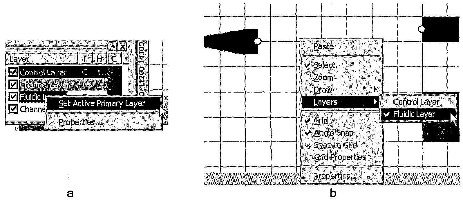
FIG. 11 shows a microfluidic valve symbol of an embodiment of the present invention. The fluid channel 262 has input end 263 and output end 264. The confrol channel 266 has input end 267 and a closed output end 268. When fluid (liquid or gas) flows in the control channel 266, the fluid channel 262 it is shut off and the fluid (liquid or gas) stops flowing, i.e., the valve 260 is turned on. Otherwise, the valve 260 is normally off (i.e., open) and the fluid (liquid or gas) in the fluid channel 262 keeps flowing. The valve in FIG. 11 is a multilayered symbol. The fluid channel is on a different layer from that of the control channel. From Fig. 12, for illustration purposes, let layer 1 335 represent the confrol layer and layer 0 334 represent the fluid layer. Then with layer 0 334 selected and layer 1 unselected the fluid channel 262 is displayed and can be connected to another fluid channel. With layer 0 334 unselected and layer 1 selected the control channel 266 is displayed and can be connected to another control channel. FIG. 12 illustrates a schematic capture display window 310 according to an embodiment of the present invention. The window 310 includes an area showing the library components 312, an area 314 showing the layers selected and an active drawing area 316 were the component symbols from active library area 320 are dragged and dropped and connected together. The layered area 314 is used when there are multilayered component symbols in library components area 312. The layered area 314 controls which layer(s) in the active drawing area 316 is/are active. If, for example, only one layer is active then only the components or parts of components on that layer are displayed and can be modified or acted upon. The layers include major layers, for example, layer n 338, layer 1 335, and layer 0 334, and sub-layers, for example, inter-layer n 336 and inter-layer 0 337. The sub-layers are layers in between the major layers. For ease of viewing each layer may have its own associated color for the channels on that layer.
FIG. 13 A shows an example of a peristaltic pump 342 connected to a T-switch 344 in an expanded drawing area 340 of the window 310 of FIG. 12 in an embodiment of the present invention. The peristaltic pump 342 is a basic component that allows the active control of fluid in either direction. Each of the control channels 348-1, 348-2, and 348-3, are pressurized (and depressurized) in some order to create a pumping effect in the fluid channel 364. The T-switch 344 represents a basic component that is used to direct the incoming flow 360 in the fluidic channel to none or one of two channels, 362-1 or 362-2, based on the state of the control channels 350-1 and 350-2. The peristaltic pump 342 is first selected from the
active library/palette area 320 and dragged and dropped into the drawing area 316. Next the T-switch is selected and dragged and dropped into the drawing area 316. The peristaltic pump 342 is then connected to the T Switch 344 via a fluid channel 346. The function of the microfluidic network in FIG. 13A is to pump a fluid into one of two directions 362-1 or 362- 2.
FIG. 13B shows an example of using IDEFO blocks to perform schematic capture in another embodiment of the present invention. The peristaltic pump 342 has input 364 and control bus 348 having three control lines. The output of the peristaltic pump 342 is connected via line 346 to the T-switch 344. The T-switch 344 has a control bus 350 having two lines and an output bus 362 having two lines. The microfluidic network schematically captured in FIG. 13B is the same as that of FIG. 13A, but with more abstract symbols.
As shown in FIG. 8, from the schematic entry 202, a design database 220 is produced that represents the interconnected components. This design database 220 serves as input into the functional analysis 360 and the physical implementation 400.
Functional Analysis ("Phase 3)
After completion of the schematic design entry, a good design practice to reduce the number of design iterations is to functionally simulate the design. Functional simulation of microfluidic circuits involves application of control signals to the active components of the design and shows the functional/static behavior of the design without regard to the dynamic behavior of the fluid within the device. Examples of active fluidic components include valves and pumps which act on the fluid. A fixed channel is an example of a passive fluidic component. Functional libraries 362 for the component models are provided for each component (FIG. 1). In one embodiment the component functional models are computer programs written in C, C++, VHDL, Verilog, Verilog- A, VHDL-AMS, or Verilog- AMS, and are executed by a commercial simulator, such as from Synopsys, Inc. of Mountain View, California, or Cadence Design Systems, Inc. of San Jose, California.
FIG. 14 shows a block diagram for the connected component functional models of the functional analysis 360 of the MCAD system 10 according to an embodiment of the present invention. Components are extracted from the schematic design database 220 and are used to select the associated component functional models from the functional simulation library 362 (FIG. 1). These component functional models are connected together as given by the schematic design database 220 for the microfluidic circuit being simulated.
In one embodiment of the present invention, the logical fluidic flow simulation 366 simulates the confrol logic of the active microfluidic components (FIG. 1). The purpose is to give an initial validation of the logic control 364 and to insure proper connectivity in the microfluidic circuit. In this case the functional models in the functional simulation library 362 includes models defined as Boolean expressions with operands based on the control port(s) 376 of the active component which control connections to the input ports 372 and the output ports 374. Valid Boolean operators are as follows: * = AND, + = OR, Λ = XOR, ! = NOT.
For example, a simple valve component with a single input port and a single output port and a control port can be defined as follows:
Input — I, Output = O, Control = C
Functional Model Valve
Port I: input
Port O: output Port C: control
0 =I * C
When C = H (or ' 1 '), then the output O gets the input I. When C = L (or '0'), then O = L regardless of the value of the input I.
Logical fluidic flow simulation 366 of the logic confrol 364 of the testing apparatus that will actuate the active components (FIG. 1) is created using the diagnostic device control language or diagnostic chip control language (DCCL) 380, as shown in FIG. 14. The DCCL 380 is a simple Boolean based language with timing constraints that can generate control signals to simulate actuation of the device's active components and read and log data from detection ports 378 of the functional models 370. Any additional physical. characteristics of the control and input signals can be included for the physical simulation but are ignored in the functional simulation. Consequently, the same DCCL program can be used in the actual testing when the device is ultimately fabricated and put into use by the user. The results of the simulation are shown in the functional analysis results 382 and are displayed as a series of square waves that indicate valve position, path connectivity, detection, control signal generation, etc.
In another embodiment the functional models are VHDL or Verilog models. A valve can be represented by the VHDL expression:
O <= I and C after 5 μsec; where "and" is a Boolean operator and there is a delay of 5 μsec before the result of the and operation is assigned to O. The DCCL of the above embodiment is represented in this embodiment as a typical VHDL test bench. As seen in FIG. 14 the test bench supplies over
time the inputs to some of the input ports 372, primarily to the input ports 372 associated with the inputs to the microfluidic circuit given by the connected functional models 370. The test bench analyzes the output ports 374 associated with the outputs of the microfluidic circuit given by the connected functional models 370. The test bench also monitors intermediate points in the connected functional models 370 by monitoring various detection ports 378. The functional analysis results 382 may be displayed by a commercial VHDL simulator as timing diagrams or waveforms.
In yet another embodiment VHDL-AMS or Verilog- AMS is used to represent the Functional Models 370. The inputs into the control ports 376 are typically digital, while the functional transformation of values from the input ports 372 to the output ports 374 are given by analog functions. Thus a first order dynamic analysis may be done. This allows an intermediary analysis between the static connectivity analysis and the physical analysis 800 given by phase 6 (FIG. 1).
In a further embodiment an analysis of the fluid flow only may be performed in a way similar to that for passive microfluidics (see "Passive Microfluidics - Ultra-Low- Cost Plastic Disposable Lab-On-A-Chips," by Bernard H. Weigl, et. al., in Proceedings of Micro Total Analysis Systems 2000, Dordrecht, Netherlands: Kluwer Academic Publishers, 2000, p. 299). Assuming the fluid is flowing through the fluid channels and the pertinent control channels are turned on, the microfluidic circuits may be represented by analog electrical components, such as capacitors, resistors, and inductors, to predict fluid flow rates. Diffusion and chemical reactions may be calculated using finite element analysis. Thus an initial analysis of the fluid flow and fluid mixing through the fluid microcircuits may be obtained. This again is neither a static nor a full dynamic analysis, but somewhere in between, i.e., an intermediary analysis.
Physical Implementation (Phase 4)
Once the schematic design has been completed and functionally tested, the physical implementation of the schematic into a physical layout takes place. FIG. 15 shows a block diagram of the physical implementation 400 according to an embodiment of the present invention. The design database also is developed based on the schematic entry 202, as shown in FIG. 8 and described above. The design database 220 represents the interconnected components which are then assigned to physical layers, via a place and route routine, either automatically or manually.
While a tool such as AutoCAD® from Autodesk, Inc. of San Rafael, California, may be used to physically lay out a microfluidic circuit, it has several disadvantages. AutoCAD® has no drawing constraints as it is a general tool. Hence, for example, a control channel can overlap a fluid channel causing an unwanted parasitic valve. While this tool is capable of multiple layers, components are typically drawn on one layer only. Manipulation of a multilayered component presents serious difficulties. AutoCAD® does not have the concept of an I/O port and connectivity to an I/O port. Again since AutoCAD® is a general CAD program, there is no design information associated with a component such as functional information. Embodiments of the present invention overcome these disadvantages of AutoCAD® and other similar tools, and provide a system in which a microfluidic circuit can be easily and efficiently created using multilayered microfluidic components on a physical layout. There are two primary aspects to the physical layout 410 of the microfluidic circuit or system or device. The first is component placement and the second is the routing of the interconnections between the placed components. Components can be either manually or automatically placed in the MCAD system's placement tool. The placement tool includes one or more of the following functions: allowing the grouping of components by connectivity by layer and/or by cross layer (3D grouping); placing components based on design rule constraints (DRC) in the DRC database 424 from set mechanical properties per layer provided in the mechanical properties library 422; performing design rule checking 420; allowing for grid and gridless placement of components; highlighting DRC errors; performing layer to layer shrinkage compensation for placements; and/or reading and writing the DWG, DXF, or other appropriate file formats.
Examples of DRC s include checks on I/O placement, channel size mismatch, dangling channels, overlapping components & channels, and channel spacing. An I/O placement rule may restrict a user to a set of pre-defined templates having pre-defined I/O ports. FIGS. 16A and 16B give examples of pre-defined templates of an embodiment of the present invention. For example, a template 440 may correspond to a microfluidic chip that is approximately a 20 mm x 20 mm square in size and about 4 mm thick. The I/O ports 442 and 444 correspond to a large via about 3 mm and a small via about 625 μm, respectively. In an alternative embodiment the user may create his/her own template and may place the I/O ports on the user-designed template.
A channel size mismatch rule allows checks for component channels (i.e., channels that are part of the component) to connecting channel having size mismatch and channel-to-channel size mismatch.
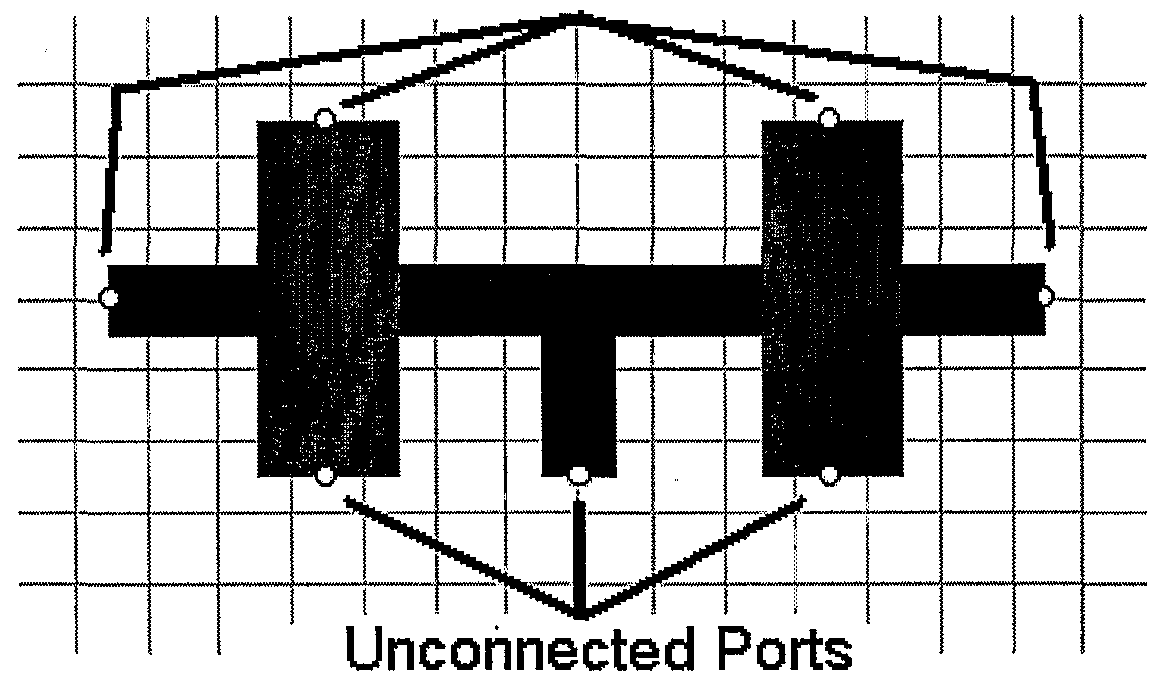
A dangling channel checking rule checks for two or more unconnected ports per component channel (only one end of a component channel need be connected) and for only one connected port on a user drawn channel (both ends of channels must be connected).
An overlapping channels rule allows checking for overlapping user drawn fluidic and control channels. There is an error for any overlapping channels. If there is auto- bridging then one or both channels are re-shaped at and within a predefined distance of the overlap point and no error occurs. Other overlapping components & channels rules check for overlapping channels on the same layer and overlapping components on the same layer or on another layer. Again if there is auto-bridging, two overlapping channels on the same layer may be corrected by routing one channel to another layer and back again using vias.
A channel spacing rule checks for minimum spacing between adjacent channels of a predetermined width. For example, there may be required a minimum of 30 μm between adjacent 120 μm width channels, a minimum of 50 μm between adjacent 100 μm width channels, and a minimum of 70 μm between adjacent 80 μm width channels,
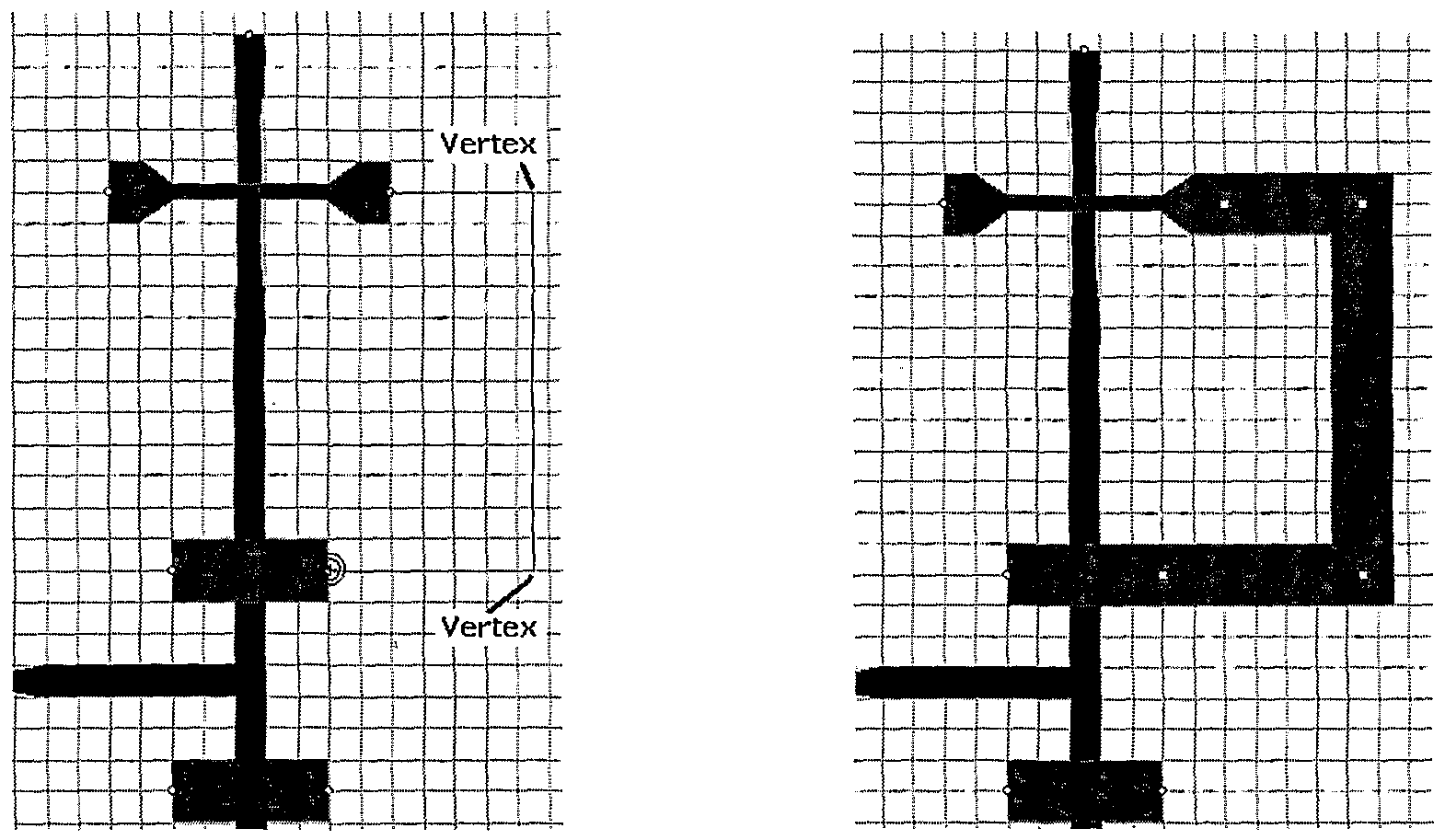
Next the interconnections between the placed components can be either manually or automatically done in the MCAD system's routing tool. The routing tool includes one or more of the following functions: definition of routing cross-sectional profiles; auto-routing 430 for similarly pitched components - grid or gridless; optimization of routing corners: right angle, radius, etc.; relocation of routing to other layers; layer to layer shrinkage compensation; and/or auto-bridging either intra or inter layer, where inter-layer bridging is done using vias. In an embodiment of the present invention there are two types of bridging performed by the auto routing 430 (FIG. 15). The first type is an interconnect bridge channel which is used when a control channel on one layer overlaps a fluid channel on an adjacent layer. The interconnected bridge channel prevents the fluid channel from being closed when the control channel is activated. The second type is needed, when there is a crossing between a first and a second channel on the same layer. This type of bridge uses vias to reroute the first channel to another layer to detour around the second channel.
FIG. 17A shows the physical dimensions for an interconnect bridge channel 460 of an embodiment of the present invention. The interconnect bridge channel has channel
width 462 and channel length 464. Both ends of the interconnect bridge channel have widths greater than the middle portion with one end having interconnect width 466 and the other and having interconnect width 468.
FIG. 17B shows a symbol for an interconnect bridge of one embodiment of the present invention. The fluid channel 470 is on a first layer with ends 472 and 474. The control channel 476 is on a second adjacent layer with ends 480 and 478. The control channel 476 is an interconnect bridge similar to that shown in FIG. 17A and it overlaps the fluid channel 478 at overlap area 482. The control channel 476 goes from a first channel width at end 478 through a taper element to a narrow channel width and through a taper element back to the first channel width at end 480. The fluid channel 470 is tapered in the middle near overlap area 482. The tapering is done to reduce the ability of the control channel to inhibit the flow in the fluid channel 470. The control channel 476 when activated does not stop the flow through fluid channel 470 and thus effectively bridges the fluid channel 470. FIG. 18A shows a crossing of two channels located on the same layer. In order to get from point 485 to point 488 and from point 486 to point 489 without going around any of the points, channels 490 and 492 must cross. In order to prevent this crossing, channel 490 must be detoured to another layer (alternately channel 492 could be detoured). FIG. 18B shows an interconnect bridge channel using vias of an embodiment to of the present invention. From point 485 channel 491 on layer 496 is detoured through a via 493 to an adjacent layer 498 to channel 495. Channel 495 on layer 498 goes underneath channel 492 and then goes backup through via 494 to channel 497 to point 488. Thus channel 492 is bridged using another, but not necessarily adjacent, layer. In another embodiment channel 492 is detoured around channel 490. FIG. 19 shows a physical layout tool according to one embodiment of the present invention. Typically, the difference between the design schematic capture 200 (phase 2) and the physical layout schematic 400 (phase 4) is that the former shows interconnected functional components without regard to placement on a template, while the latter takes into account the physical location on a template. In the physical layout 410, the physical characteristics of a microfluidic component are just as important as the functional characteristics of a component (both active and passive). In a schematic capture the symbols representing a component may be abstracted (e.g., FIG. 10) and the symbols are placed and connected, and no physical routing takes place. Also the placement in the schematic is not necessarily related to where the microfluidic component is physically located in the
manufactured microfluidic chip or device. In a physical layout where the microfluidic component is placed is related to where the component is physically located. And routing places channels between microfluidic components to physically connect them.
For this embodiment, phase 1 to phase 3 are not performed and the user begins with phase 4. In this embodiment, the basic library 206 and macro library 210, which together include the components for the physical layout 410, feed the layout tool 510 directly and the schematic entry 202 is bypassed. In FIG. 19 the layout tool 510 displayed includes a component library area 512, a layer area 520, an active drawing area 530 and status bar 535. The component library area 512 includes the library components, represented by symbols, that are available for the layout design. To select the portion of the library desired, one simply left clicks on the title of the portion (e.g., bridges 514, channel arrays 516, or pumps 517), and the components are displayed (e.g., active area 520 of bridges 514). If more than one component is present in the active area the up or down button is used to scroll through them. Once the proper component is found, one may left click the mouse button and hold and drag the component into the active drawing area 530 and release the button to place the component in a desired location.
A library component is typically composed of channels. Some components have channels only on one layer while some have channels on two or more layers. FIG. 20 shows a symbol for a microfluidic valve of one embodiment of the' present invention. The black line 537 represents a fluid channel present on the fluidic layer while the gray line 538 represents a channel on the control layer. The colors have been picked for illustration purposes only and other colors such as blue for a fluid channel and red for a control channel are equally acceptable. The connection ports 540 are points where connections from other components or channels are allowed to be made with the valve component. Additional examples of the symbols or icons for the microfluidic components are provided below.
The layer area 520 in FIG. 19 indicates the coloring/shading of the layers as well as the different channel heights that are available in the particular layer. For example, control layer 522 and fluidic layer 524 are selected and thus both fluidic and control channels are shown in active drawing area 530. There are two categories of layers: primary layers, e.g., control layer 522 and fluidic layer 524, and channel layers, e.g., 523 and 525, in FIG. 19. The primary layer has a type, such as control or fluid, and includes one or more channel layers, e.g., control layer 522 has one channel layer 523, and fluid layer 524 has one channel layer 525. Channel layers inherit their type from their parent primary layer. Channel layers
own channels, for example, drawn by the user or by auto-routing, in the active drawing area 530. Channels in a component, when placed on the drawing area 530, are linked to these user (or auto-route) drawn channels in the corresponding channel layer via the associated primary layer. The active drawing area 530 is where components from the component library area 512 are placed and connected together using the drawing tools. In one embodiment the active drawing area includes a predefined template 532. The predefined template 532 has a plurality of I/O ports, for example 534-1, 534-2, 534-3, and 534-4. the components in component library area 512 are placed and connected on this template 532. Also connections are made from the connected components to the I/O ports.
The status bar 535 has two modes for the drawing area 530. One mode for the drawing area is the select mode (shown in FIG. 19) and the other is the channel drawing mode (not shown). In the select mode the status bar includes the following information: (1) Left Status Box: Component Name; (2) Center Status Box: Absolute Cursor Location (in microns); and (3) Right Status Box: Percentage Zoomed In. In the drawing mode (not shown) the status bar includes the following information: (1) Left Status Box: Length of channel drawn (in microns); (2) Center Status Box: Absolute Cursor Location (in microns); and (3) Right Status Box: Percentage Zoomed In.
FIG. 21 shows two components of an embodiment of the present invention. The two components shown on an expanded template area 545 are a rotary pump 544 and a channel array 547. The rotary pump 544 shown has a fluid channel 580 and two fluid ports 576 and 577 (FIG. 23). The rotary pump 544 is provided for mixing and incubating solutions by employing one or more pumps to flow solution around a circular flow channel. See, e.g., Stephen R. Quake and Axel Scherer, "From Micro- to Nanofabrication with Soft Materials," Science 290: 1536-40 (2000). The three channel array 547 provides a set of individually addressable flow lines 582, 584, and 586 (FIG. 23). The number of control lines is equal to the number of fluid lines for this array component. The flow of the liquid within the array can be controlled by actuating the necessary control lines.
FIG. 22 shows the control channels on the control layer for the two components of FIG. 21. In the layer area 520 the fluidic layer 524 is not selected and the control layer 522 is selected. This allows only the channels on the control layer to be viewed on the active drawing area 530. For the rotary pump 544 the control channels are 562, 564, 566, and 568. For the channel array 547 the three control channels are 570, 572, and 574. Channels 572 and 574 have narrow channel regions 571 and 573, so that the fluid channel
582 in the case of control channel 572 and the fluid channels 582 and 584 in the case of control channel 574 are not shut when control channel 572 or 574 is activated.
FIG. 23 shows the fluid channels for the fluid layer for the two components of FIG. 21. In the layer area 520 the fluidic layer 524 is selected and the control layer 522 is not selected. This allows only the channels on the fluid layer to be viewed on the active drawing area 530. For the rotary pump 544 there is one fluid channel 580 with two I/O ports 576 and 577. For the channel array 547 there are three fluid channels 582, 584, and 586.
FIG. 24 shows a partially connected layout of a microfluidic circuit having a rotary pump 544 and a channel array 547 according to an embodiment of the present invention. In the layer area 520 both the control layer 522 and the fluidic layer 524 have been selected. Hence both control and fluid channels are displayed on expanded template area 545. I/O port 534-1 is connected to the array pump 544 via fluid channel 590. Rotary pump 544 is connected to channel array 547 via the fluid channel 592. Channel array 547 also receives input from I/O port 534-6 via fluid channel 594. Control channels for rotary pump 544 include control channel 591 from I/O port 534-5 and control channel 595 from I/O port 534-7. Control channel 595 is tapered to a narrow channel 596 to bridge fluid channel 594 (interconnect bridge of FIG. 17B). Fluid channel 594 may also be tapered to a narrow fluid channel 597 to further insure that control channel 595 does not shut off fluid channel 594 when control channel 595 is activated. In one embodiment, if a user tries to draw a control channel 598 as shown in
FIG. 24, a design rule check gives an error that valves are formed at the overlap points 599-1 and 599-2. The user is not allowed to add control channel 598 to expanded template area 545. In another embodiment interconnect bridges would automatically be formed at overlap points 599-1 and 599-2. FIG. 25 shows a flow chart having the steps involved in the physical layout of a microfluidic circuit according to an embodiment of the present invention. At step 602 a chip template is selected from, for example, a plurality of templates such as those shown in FIGS. 16A and 16B. The layers, including the control and fluid layers, are selected and modified (step 603). At step 604 components are selected from the component library area 512 (FIG. 19). At step 605 these components are placed on the template. The placed components are connected (step 606), either manually or via an auto-route routine by channels. For example, the components' control channels are first connected together on the confrol layer using control channels. Next the components' fluid channels are connected together on the fluid layer using fluid channels. At step 607 some of the components are
connected to the I/ ports on the template. At step 608, the design topology of the microfluidic circuit may be manually or automatically verified.
In one embodiment the control channels are not connected to the fluid channels. In another embodiment, although the control channels may be on different layers than the fluid channels, they may be connected to the fluid channels by vias.
FIG. 26 shows a pressure oscillator structure of one embodiment of the present invention. The pressure oscillator operates analogously to oscillator circuits frequently employed in the field of electronics. The pressure oscillator includes a fluid channel 610 which has an imtial portion 611 proximate to a pressure source 612, and a serpentine portion 614 distal from pressure source 612. Initial portion 611 is in fluid communication, through via 616, with control channel 618 formed above the level of fluid channel 610. At a location more distal from pressure source 612 than via 616, control channel 618 overlaps, but is separated from, fluid channel 610, thereby forming a valve 620.
The pressure oscillator structure operates as follows. Initially, pressure source 612 provides pressure along fluid channel 611 and control channel 618 through via 616. Because of the serpentine shape of flow channel 614, pressure is lower in region 614 as compared with control channel 618. At valve 620, the pressure difference between serpentine flow channel portion 614 and overlying control channel 618 eventually causes valve 620 to close. Owing to the continued operation of pressure source 612, however, pressure begins to build up in serpentine flow channel portion 614 behind closed valve 620. Eventually the pressure equalizes between control channel 618 and serpentine flow channel portion 614, and valve 620 opens. Given the continuous operation of the pressure source 612, the above-described build up and release of pressure will continue indefinitely, resulting in a regular oscillation of pressure. Such a pressure oscillation device may perform any number of possible functions, including but not limited to, timing.
An illustration of an application developed using the physical layout tool of FIG. 19 and the steps of FIG. 25 is a cell sorter shown in FIGS. 27 and 28.
FIG. 27 shows a physical layout of a cell sorter of an embodiment of the present invention. The template 630 is located in active drawing area 530 and has one fluid input port 634, two fluid output ports 636 and 638, and five control input ports 642, 644, 646, 648, and 640. Fluid input port 634 is connected to fluid channel 650. Fluid channel 650 forks to fluid channel 652 and fluid channel 654. Fluid channel 652 is connected to output port 636 and fluid channel 654 is connected to output port 638. Input control port 642 is connected to control channel 660. Input control port 644 is connected to control channel 662.
Input control port 646 is connected to control channel 664. Input control port 648 is connected to control channel 668. Input control port 640 is connected to control channel 666.
FIG. 28 shows an expanded view 710 of the physical layout of the cell sorter of an embodiment of the present invention. A pump 712 includes a peristaltic pump 714 and a damper element 716. The pump 712 includes a peristaltic pump 714 which is composed of three individual valves with control channels 642, 644, and 646. The liquid within the fluid channel 650 is pumped by sequentially actuating the individual valves. The damper element 716 is used to provide a smoother flow of pumped fluid. The membrane of the damper element 716 will deflect and absorb the energy caused by the closing of the valves of the peristaltic pump 714. The fluid from fluid input port 634 is pressurized by pump 712 and enters, via a fluidic taper 718-1, a narrow channel 720 which is a detection region 724. The narrow channel 720 is connected to a T-sorter 722 by another fluidic taper 718-2. The fluid in the T-sorter 722 either proceeds to the fluid output port 636 or the fluid output port 638, depending on whether control channel 666 or control channel 668 is activated. The microfluidic circuit of FIGS. 27 and 28 is laid out according to the steps given in FIG. 25 as follows. First a template 630 is selected (step 602) and placed in drawing area 530. The template has six large I/O ports (e.g., I/O ports 634, 636, and 638 of 3 mm in size) and 12 small I/O ports (e.g., I/O ports 640, 642, 644, 646, and 648 of 625 μm in size). Next at step 603 the layers are selected in layer area 520. From the component library area 512 (FIG. 19), one pump 712, one T-sorter 722, two fluidic tapers 718, and two interconnect bridges 732-1 and 732-2, are dragged and dropped on the template 630 as shown in FIG. 28 (steps 604 and 605). Step 606 has two parts, and involves first connecting the fluid channels of the components by drawing fluid channels on the fluid layer, and second connecting the control channels of the components on the control layer (in this case the connections are only to the template's I/O ports). When the fluid layer is selected, the pump 712 is connected to a first fluid taper 718-1, and via a narrow channel 720 to a second fluid taper 718-2 (see FIG. 28). The narrow fluid channel is created by drawing a normal fluid channel with default width of, for example 100 μm, and then selecting a new channel width of, for example, 30 μm. The second fluid taper 718-2 is connected to the T-sorter 722. At step 607 the T- sorter's fluid channels are connected to I/O ports 636 and 638 on the fluid layer using fluid channels 652 and 654. The control channels of the pump 712 and T-sorter 722 are connected to the I/O ports, 642, 644, 646, 640, and 648, using control channels, 660, 662, 664, 666, and 668, drawn on the control layer. In the case of the T-sorter 722, interconnect bridges 732-1
and 732-2 are used, so that control channels 666 and 668 can bridge the fluid channels 652 and 654 without creating parasitic valves. At step 608 the microfluidic circuit on template 630 is checked for errors. For example a DRC may be done. In an alternative embodiment of the present invention, after the components have been placed on the template 630 (step 605), an auto-routing routine may connect the components with channels (step 606). In another embodiment the design rule checks may be done interactively as each entry in active drawing area 530 is made.
The operation of the sorting device in accordance with one embodiment of the present invention is as follows. The sample is diluted to a level such that only a single sortable entity would be expected to be present in the narrow channel 720 at any time.
Assume, for the sake of illustration, that the sortable entity is either size A or size B and that size A entities are collected at fluid output port 636 and size B entities are collected at fluid output port 638. Pump 712 (three confrol valves and five damping elements) is activated by flowing a fluid through control channels 642, 644, and 646 as described above. The sortable entity enters via input port 634 and moves via fluid channel 650. The sortable entity is pushed by the pump 712 into the narrow channel 722. The narrow channel width is selected such that the sortable entities can move only in a single file manner through this channel. Hence if there happen to be two sortable entities in the narrow channel 722, one must follow the other. The narrow channel 722 serves as a detection region 724, where an external detection system, such as an optical measurement system, is used to determine if the detected sortable entity is size A or size B. The bridge components 732-1 and 732-2 are used to allow crossing of the fluid lines by the control lines without creating a parasitic valve. The bridge components are also used to create an area clear of channels for the detection region 724. If the sortable entity is size A then control channel 668 is activated and control line 666 is deactivated. This turns on the valve 750 and turns off valve 752. Hence the size A entity flows to fluid output port 636. If the sortable entity is size B then control channel 666 is activated and control line 668 is deactivated. This turns on the valve 752 and turns off valve 750. Hence the size B entity flows to fluid output port 638.
Sorting in accordance with the above embodiment would avoid the disadvantages of sorting utilizing conventional elecfrokinetic flow, such as bubble formation, a strong dependence of flow magnitude and direction on the composition of the solution and surface chemistry effects, a differential mobility of different chemical species, and/or decreased viability of living organisms in the mobile medium. For more detailed discussions of cell sorting by microfabricated devices, see A. Y. Fu et al, "A Microfabricated
Fluorescence-Activated Cell Sorter," Nature Biotechnology 17: 1109-1111 (1999); H. P. Chou et al., "A Microfabricated Device for Sizing and Sorting DNA Molecules," Proc. NatT Acad. Sci. 96: 11-13 (1999); S. Quake et al., "Disposable Microdevices for DNA Analysis and Cell Sorting," Proc. Solid-State Sensor and Actuator Workshop," Hilton Head, S.C., June 8-11, 1998, pp. 11-14; and H. P. Chou et al., "Microfabricated Devices for Sizing DNA and Sorting Cells, Micro- and Nanofabricated Structures and Devices for Biomedical Environmental Applications," Paul L. Gourley, Editor, Proceedings of SPIE Vol. 3258, 181-7 (1998).
Further details on the physical layout tool is given by the User's Manual as provided below.
Object-Oriented Design of Physical Layout (Phase 4)
As illustrated by the above embodiments, one major feature of an embodiment of the present invention is a microfluidic channel (herein called a channel or channel object), for example, a fluid or control channel, that may be used to form a microfluidic component, e.g., the valve of FIG. 20, to connect two microfluidic components, e.g., fluid channel 592 of FIG. 24 connecting a rotary pump 544 to a 3-array 547, or to connect an I/O port to a microfluidic component, e.g., control channel 591 of FIG. 24 connecting I/O port 535-5 to a rotary pump 544. In the case of an active microfluidic component, in one object oriented embodiment, the active microfluidic component symbol is constructed using at least one control channel object as part of one symbol layer object and at least one fluid channel object as part of a different layer object. An example, is a valve symbol with two symbol layers; one symbol layer having a fluid channel and a second symbol layer having a control channel.
Fig. 28-1 shows a simplified UML diagram of the object relationships of an embodiment of the present invention. The model is a "canvas" which provides the main container for all objects in one embodiment of the present invention. The model class is CMDCModel 812 (CMDC stands for Class Mycometrix Design Capture, and precedes all class names). The CMDCModel 812 owns three types of FluidArchitect objects: CMDCSymbolComponent 820, CMDCIOPortComponent 814, and CMDCPrimaryLayerComponent 830. CMDCSymbolComponent 820 has children of type CMDCSymbolLayerComponent 822, which in turn has children of type
CMDCChannelComponent 824, which in turn has children of type CMDCPortComponent 826. CMDCPrimaryLayerComponent 830 has children of type CMDCInterLayerComponent 832, which in turn has children of channel objects 834, which in turn have children of type CMDCPortComponent 836. Note that the CMDCPortComponent 826 and
CMDCPortComponent 836 are the same class The diamond(s) 808 indicate in the Unified Modeling Language (UML) aggregation (part-whole relationship). For example, a primary layer object of class CMDCPrimaryLayerComponent 830 is "part of the model object of the CMDCModel class 812. To simplify the explanation, from here onward instantiation of classes, or objects, will be used when referring to the item numbers in Fig. 28-1. The model object 812 owns the primary layer objects 830 (CMDCPrimaryLayerComponent), of type, for example, fluidic/fluid or control. The model object 812 doesn't own channel objects 834 directly; rather it owns the primary layers which own the channel layer object(s) 832 that own the channel objects 834. Also the model object owns the symbol objects 820 of the microfluidic components (CMDCSymbolComponent), for example, the symbol (i.e., symbol object) for the valve (FIG. 20), and further owns the Input/Output port objects 814 (CMDCIOPortComponent). In addition the model 812 provides hit testing of the entire design, validating operations on channels (move, resize, etc) and various DRC's (Design Rule Checks). The primary layers objects 830 (CMDCPrimaryLayerComponent) are part of the model object 812 (CMDCModel). The model includes one or more primary layers. Primary layers 830 are layers that include one or more channel layers 832. A primary layer 830 has a used defined height that is at least the sum of all its channel layer's 832 heights. Primary layers 830 are typed to describe their functionality, for example, fluidic/fluid and control types.
The channel layer objects 832 (CMDCInterLayerComponent) are owned by the primary layer objects 830. A channel layer may only be owned by one primary layer. A channel layer 832 owns zero or more channel objects (i.e., channels) 834. A channel layer has a user-defined height that all channels, i.e., channel objects 834, on the layer will inherit. Channel layers 832 only have a type of Interlayer. They inherit their primary layer's type for functionality. Channel layers 832 own the actual channels 834, e.g., fluid or control channels, that the user draws using the drawing tools. Channels 824 contained in symbols 820 are not owned by the channel layer 832 (CMDCInterLayerComponent), but when the symbol is placed on the drawing area, these channels 824 are associated to the appropriate channel layer 832. This allows the channel layer 832 access to all channels, e.g., channels 834, that are placed on that channel layer 832.
A model 812 may include a symbol object for a microfluidic component (CMDCSymbolComponent), or symbol 820 for short. Symbols are added to the drawing area or canvas via a drag and drop method. A symbol object 820 owns one or more symbol
layer objects 822 (CMDCSymbolLayerComponent). A symbol layer object 822 owns zero or more channel objects 824 (CMDCChannelComponent). Symbol layers 822 are matched up with the primary layers 830, either via an "active" layer, or through user input. A channel object 824 from the symbol layer 822 is linked to a channel layer 832 via the associated primary layer 830. The channel object 824 is associated to either the "active" channel layer 832 or a channel layer 832 selected by user input. The channel layer 832 and corresponding primary layer 830 have no control over the existence of the linked channels 824 from the symbol layer 822.
The channel objects 824 and 834 (CMDCChannelComponent) own port objects 826 and 836 (CMDCPortComponent) respectively. These ports 826 and 836, are children of the channel objects 824 or 834, which allow connections to other ports. This facilitates the connection of channel objects 824 and 834 to each other. Any data member that is specific to a particular type of channel is stored in that channel's structure. All data members that are general to all channel components are stored in the CMDCChannelAdapter. Examples of different types of channels include: 1 ) a polyline channel
(CMDCChannelComponent) having a line of N vertices. It is a straight polyline channel with basic line functionality. This channel is a line with a user specified width. It has a port at each end of the line for connection to other channels; 2) an arc Channel (CMDCArcChannelComponent) which like the CMDCChannelComponent, provides basic line functionality. The CMDCArcChannelComponent requires 3 vertices to form an elliptical arc channel. The arc channel has 2 ports, one at either end of the arc; 3) an ellipse Channel (CMDCEUipseChannelComponenf) which provides an elliptical channel. This channel also has a user specified width. It has ports at the top, bottom, left and right of the ellipse; 4) a funnel channel (CMDCFunnelChannelComponent) which is used to connect two channels of differing widths. The funnel channel has only two vertices. The funnel channel inherits the widths from its port connections; and 5) a Rectangle Channel
(CMDCRectangleChannelComponent) which provides a solid filled rectangle channel. The rectangle channel has ports on the left center, right center, top center, and bottom center of the rectangle. The rectangle does not make use of the width variable, as it is a filled rectangle.
Channel objects are owned exclusively by layers, with the exception of the I/O ports. Channels 824 that are part of symbols 820 are owned by symbol layers 822 and are associated with channel layers 832 when they are added to the design. Channels 824 and 834
own ports 826 and 836 respectively. Some channel types have a fixed number of ports; other types allow any number of ports.
The model 812 further includes I/O Ports (CMDCIOPortChannelComponent)
814. These are the actual input and outputs into the design. The model object itself 812 owns the I/O port objects 814 so any layer of the design can access them. Unlike other channels, these channels are, in some cases, predefined on a template. They accept connections from any of the other channels 824 and 834.
Thus a first microfluidic component symbol object in one embodiment of the present invention has a plurality of symbol layer objects, where each symbol layer object represents a different layer. A first symbol layer object has a first fluid channel object and a second symbol layer object has a first control channel object. Similarly, a second microfluidic symbol object has two symbol layer objects: a third symbol layer having a second fluid channel object and a forth symbol layer having a second control channel object.
The fluid channel objects of these two microfluidic component symbol objects are linked, i.e., connected, together in the model object 812 via a channel object 834 as part of a channel layer object 832 via the port objects 826 and 836 of their respective channel objects. Hence, the first fluid channel object on the first symbol layer is linked to the channel object 834 via the channel layer 832; and the second fluid channel object on the third symbol layer is linked to the channel object 834 via the channel layer 832. Thus a fluid channel of a first active microfluidic component placed on a template is connected to a fluid channel of a second active microfluidic component placed on the template using a passive channel drawn by a user (or via an auto-route routine).
Further details on the object-oriented design is given below.
Physical Analysis (Phase 5)
Once the design has been completed, placed, and routed, a simulation indicating the dynamic performance can be performed under physical analysis 800 (phase 5). As shown in FIG. 1, dynamic simulation models 810 of the components are based on the physical attributes as well as the chosen material properties for the layer in which the component is placed, as provided in the mechanical properties library 820. Fluid characteristics are also taken into account as well as the confrol signal's actual actuation pressures. The physical analysis 800 in the MCAD system 10 includes one or more of the following: dynamic volumetric flow rates, volumetric capacitances of components,
volumetric capacitances of interconnect/routing channels, parasitic layout extraction 830 and/or parasitic components.
In one embodiment the dynamic fluidic flow simulation 840 is performed using ANS YS/Multiphysics (coupled field structural-fluid) and ANSYS/FLOTRAN™ (computational fluid dynamics) tools of ANSYS Inc. of Canonsburg, Pennsylvania (www. ansys.com/products/html multiphysics .htm and
(www.ansys.com products/flotran.htm). The ANSYS tools can perform laminar flow simulations and coupled physics simulations, such as dynamic fluidic and mechanical simulations, for microfluidic systems. Using this tool, dynamic simulation models 810 are first developed, taking into account the mechanical/structural properties of the model' s associated component (mechanical properties library 820). Next using the dynamic simulation models 810 as connected and laid out in the physical layout 410, a dynamic fluidic flow simulation circuit model for the microfluidic circuit of the physical layout 410 is developed. Parasitic or coupling effects between different channels, which are typically second order effects, optionally, may be incorporated into the dynamic fluidic flow simulation circuit model. The ANSYS/Mutiphysics tool is then used to simulate the dynamic fluidic flow simulation circuit model using a variety of test inputs. Both the final outputs and intermediate test points of the circuit model are analyzed to determine if the proper results are achieved. If not, then the physical layout 410 is modified and the associated modified dynamic fluidic flow simulation circuit model is again simulated. This iterative design process is continued until the desired results are achieved.
In another embodiment the dynamic fluidic flow simulation 840 may employ the DCCL 380 used in the functional analysis 360 as shown in FIG. 14. Device Implementation (Phase 6) Once the design has been placed and routed, the physical layout 410 of phase
4 will write out the desired chip layout files 902 to manufacture a prototype 904 of the microfluidic circuit as seen in FIG. 1. The DWG/DXF files written from the physical layout 902 can be converted to a manufacturing format, for example, Gerber, HPGL, EPS, DXF, GDS II, or Postscript, for use in device implementation 900. The layout files are then used for mask layout generation of a chip or die. Several masks are then used in step 904 to set up a wafer for manufacturing.
FIG. 29 shows a display for setting up the die layout on a wafer of an embodiment of the present invention. The die layout settings window 960 has a screen 962
which displays the die layout on a wafer 963. The screen 962 includes, a top displacement 964 from the edge of the wafer 963, a left displacement 966 from the wafer edge, an X pitch 968, a Y pitch 970 and dies, 972-1, 972-2, 972-3, and 972-4. Each die may include a microfluidic circuit such as that shown in FIG. 27. The window 960 also has a table which indicates setting values, including: wafer size 974 (e.g., 3 or 4 inches), number of dies per wafer 974 (e.g., 4 or 12), top displacement 976 (e.g., 10.4 mm or 9.2 mm), left displacement 978 (e.g., 10.4 mm or 9.2 mm), an X pitch 980 (e.g., 15 mm or 0.8 mm), and a Y pitch 982 (e.g., 15 mm or 0.8 mm).
The wafer is then manufactured (step 904) and the resulting microfluidic device is ready for either one-time use (disposable) or for continuous reuse (semi-permanent test device).
The MCAD system 10 can be implemented and executed in a variety of ways. For instance, it can be implemented as a computer-aided design (CAD) program for design, analysis, and implementation of the elastomeric circuits or networks. The CAD program can be provided separately to individual users or distributed over networks such as the Internet so that it can be centrally maintained and controlled.
Although the above functionality has generally been described in terms of specific hardware and software, it would be recognized that the invention has a much broader range of applicability. For example, the software functionality can be further combined or even separated. Similarly, the hardware functionality can be further combined, or even separated. The software functionality can be implemented in terms of hardware or a combination of hardware and software. Similarly, the hardware functionality can be implemented in software or a combination of hardware and software. 'Any number of different combinations can occur depending upon the application. Many modifications and variations of the present invention are possible in light of the above teachings. Therefore, it is to be understood that within the scope of the appended claims, the invention may be practiced otherwise than as specifically described.
The following describes a number of microfluidic components and structures from U.S. Provisional Patent Application No. 60/282,253. Fluidic Pressure Amplifier
An embodiment of a microfabricated fluidic pressure amplifier (or pressure multiplier) is shown in FIGS. 30, 31A and 3 IB. Pressure multiplier 1030 shown in FIG. 30 is a cross sectional view of a microfabricated fluidic pressure amplifier that contains pre-cured elastomer layers 1031 and 1032 that are formed on top of rigid planar substrate 1033 (e.g.,
glass). There are many, many types of elastomeric polymers. Common elastomeric polymers that maybe used to form elastomer layers 1031-1032 include polyisoprene, polybutadiene, polychloroprene, polyisobutylene, poly(styrene-butadiene-styrene), the polyurethanes, and silicones. Layer 1031 has chamber 1034, and layer 1032 has chambers 1037-1038.
Layers 1031-1032 and other elastomer layers used to form microfluidic devices may be formed and hermetically sealed together using methods discussed in further detail in PCT Patent Application Number PCT/US00/17740.
Layers 1031-1032 may be, for example, 1-1000 microns thick. Specific examples include 5, 10, 15, 20, 25, 35, 50, 60, 75, 85, 100, 150, 200, 250, 300, 350, 400, 450, 500, 550, 600, 650, 700, 750, 800, 850, 900, 950, and 1000 microns.
Chamber 1034 may be, for example, 2.5-5000 microns wide. Specific examples include 2.5, 5, 10, 15, 20, 25, 35, 50, 60, 75, 85, 100, 150, 200, 250, 300, 350, 400, 450, 500, 550, 600, 650, 700, 750, 800, 850, 900, 950, 1000, 1200, 1400, 1600, 2000, 2200, 2400, 2600, 2800, 3000, 3200, 3400, 3600, 3800, 4000, 4200, 4400, 4600, 4800, and 5000 microns.
Channel 1038 may be, for example, 0.1 - 250 microns wide. Specific examples include 0.1, 0.2, 0.3, 0.4, 0.5, 0.6, 0.7, 0.8, 0.9, 1.0, 2, 3, 4, 5, 6, 7, 8, 9, 10, 20, 30, 40, 50, 60, 70, 80, 90, 100, 120, 140, 160, 180, 200, 210, 220, and 225 microns. Layer 1035 may be, for example, 1-100 microns thick. Specific examples include 1, 2, 3, 4, 5, 6, 7, 8, 9, 10, 20, 30, 40, 50, 60, 70, 80, 90, and 100 microns.
A multilayer soft lithography process may be used to build integrated (i.e.: monolithic) microfabricated elastomeric structures. Advantages of fabricating the present structures by binding together layers of soft elastomeric materials include the fact that the resulting devices are reduced by more than two orders of magnitude in size as compared to silicon-based devices. Further advantages of rapid prototyping, ease of fabrication, and biocompatability are also achieved.
Separate elastomeric layers such as layers 1031-1032 are fabricated on top of micromachined molds such that recesses are formed in each of the various elastomeric layers. By bonding or sealing these various elastomeric layers together, the recesses extending along the various elastomeric layers form flow channels and control lines through the resulting monolithic, integral elastomeric structure. These flow channels and control lines which are formed in the elastomeric structure can be actuated to function as micro-pumps and micro- valves, as will be explained.
A top view of layer 1031 is shown in FIG. 31 A. Chamber 1034 has inlet port 1041. Layer 1035 comprises a rigid material that can be deposited on elastomer layer 1032. Rigid layer 1035 and other rigid layers used in microfluidic pressure multipliers and switches may comprise material such as polymethomethacrylate (PMMA ). Layer 1031 is then placed on top of layer 1032 so that layer 1035 is inside of chamber 1034 as shown in FIGS. 30 and 31A. A top view of layer 1032 is shown in FIG. 31B. Chamber 1037 of layer 1032 comprises two branches that surround most of chamber 1038. Chamber 1037 has inlet port 1043, and chamber 1038 has inlet port 1042.
Chamber 1037 is filled with fluid at ambient pressure P0 through inlet port 1043. Chamber 1034 is filled with a fluid at pressure Pi through port 1041, and chamber 1038 is filled with a fluid at pressure P2 through port 1042. When pressure Pi in chamber 1034 is increased above ambient pressure P0, rigid layer 1035 expands downward against chambers 1037 and 1038 causing pressure P2 in chamber 1038 to increase above Pi. The device of FIGS. 30 and 31 A-31B is a pressure multiplier. Pressure P2 is amplified to a value greater than the final value of Pi when Pi is increased above P0, according to the following equation:
P2 =aPλ -bPO -c (2)
Referring to FIGS. 30, and 31A-31B, a is the ratio of the horizontal surface area of the floor of chamber 1034 that overlaps rigid layer 1035 to the horizontal surface area of chamber 1038 that is under layer 1035, and Ms the ratio of the horizontal surface area of chamber 1037 that is directly below rigid layer 1035 to the horizontal surface area of chamber 1038 that is under layer 1035. Constant c is shown by the following equation:
AH A c=M • '32 (3)
H ■*38
where M is the bulk modulus of the elastomer layer, Η is the vertical height of chamber 1038 (FIG. 30) when Pi is at ambient pressure, ΔΗ is change in the vertical height of chamber 1038 when Pi is increased above ambient pressure and layer 1035 presses down on chamber 1038, A32 is the horizontal surface area of a cross section of elastomer layer 1032
that is underneath layer 1035 (within the dotted line 1035 in FIG. 3 IB), and A38 is the horizontal surface area of chamber 1038 that is under layer 35.
Chamber 1037 reduces the force with which elastomer material in layer 1032 presses up against rigid material 1035 when material 1035 is forced downward (with respect to FIG. 30), preserving the pressure amplification effect on P2. Pressure multiplier 1030 is advantageous, because it can be microfabricated (e.g., less than 1 mm thick). Also, the fluid in input chamber 1034 is isolated from the fluid in output chamber 1038. This may be an advantage, because the fluids in the input and output chamber of a pressure multiplier may be different types of fluids. FIG. 32 is a symbol for a pressure multiplier such as pressure multiplier 1030.
In a further embodiment, P0 need not be ambient pressure, but may be any pressure level. In this embodiment the pressure amplification system of FIGS. 30 and 31A-31B amplifies the pressure difference between Pi and P0 according to the gain factor represented in equation (2) to provide pressure P2 at the output. Microfluidic pressure multipliers may be coupled with other microfluidic devices (that are discussed in further detail below) to build devices such that perform a variety of analog functions such as integration and differentiation using configurations known to those of skill in the semiconductor circuit art. Pressure- Actuated. Normally Open Switch An embodiment of a microfabricated fluidic switch is shown in FIGS. 33A- 33E. FIGS. 33A-33D are cross sectional views of fluidic switch 1070, and FIG. 33E is a top down view of fluidic switch 1070. FIGS. 33A and 33C are cross sectional views along channel 1074, and FIGS. 33B and 33D are cross sectional views along horizontal axis 1077 illustrated in FIG. 33E. Switch 1070 includes substrate 1073, elastomer layer 1072, and elastomer layer 1071. Elastomer layer 1071 contains channel 1074, and elastomer layer 1072 contains channel 1078 and chambers 1079 A and 1079B. Channel 1074 is coupled to the gate of the switch. Channel 1078 is coupled between the source and the drain of the switch. Layers 1071-1073 may be formed and hermetically sealed using methods described in further detail in PCT Patent Application Number PCT/US00/17740.
Layer 1075 comprises a rigid material (such as PMMA) that is deposited on top of layer 1072. Layer 1071 can then be placed on top of layer 1072 so that layer 1075 is inside channel 1074. Layer 1075 is deposited on layer 1072 so that it overlaps channel 1078 and portions of chambers 1079A-1079B. A fluid is passed through channel 1074 at pressure Pi. A fluid is passed through channel 1078 at pressure P2. Channel 1074 is perpendicular to channel 1078. Chambers 1079A-1079B contain fluid at ambient pressure P0.
Layers 1071-1072 may be, for example, 1-1000 microns thick. Specific examples include 5, 10, 15, 20, 25, 35, 50, 60, 75, 85, 100, 150, 200, 250, 300, 350, 400, 450, 500, 550, 600, 650, 700, 750, 800, 850, 900, 950, and 1000 microns.
Channel 1074 may be, for example, 2.5-5000 microns wide. Specific examples include 2.5, 5, 10, 15, 20, 25, 35, 50, 60, 75, 85, 100, 150, 200, 250, 300, 350, 400, 450, 500, 550, 600, 650, 700, 750, 800, 850, 900, 950, 1000, 1200, 1400, 1600, 2000, 2200, 2400, 2600, 2800, 3000, 3200, 3400, 3600, 3800, 4000, 4200, 4400, 4600, 4800, and 5000 microns.
Channel 1078 may be, for example, 0.1 micron - 1 mm wide. Specific examples include 0.1, 0.2, 0.3, 0.4, 0.5, 0.6, 0.7, 0.8, 0.9, 1.0, 2, 3, 4, 5, 6, 7, 8, 9, 10, 20, 30, 40, 50, 60, 70, 80, 90, 100, 120, 140, 160, 180, 200, 250, 300, 350, 400, 450, 500, 550, 600, 650, 700, 750, 800, 850, 900, 950, and 1000 microns.
Layer 1075 may be, for example, 1-100 microns thick. Specific examples include 1, 2, 3, 4, 5, 6, 7, 8, 9, 10, 20, 30, 40, 50, 60, 70, 80, 90, and 100 microns. When the pressure Pi in channel 1074 is increased above P0, the radius of channel 1074 expands and rigid layer 1075 moves downwardly as shown in FIG. 33C applying pressure against channel 1078 and chambers 1079A-1079B. As Pi increases, layer 1075 presses down on the portion of channel 1078 beneath layer 1075 pinching channel 1078 closed. Channel 1078 is concave in shape making it more collapsible so that channel 1078 completely closes when Pi is increased to a predetermined level.
Chambers 1079A-1079B reduce the upward force that elastomer material in layer 1072 applies to layer 1075 when channel 1074 expands so that channel 1078 closes more quickly and completely. When channel 1074 expands to close channel 1078, fluid is displaced from chambers 1079A-1079B beneath channel 1074 into adjacent portions of chambers 1079A-1079B. Chambers 1079A-1079B provide less resistance to downward pressure on channel 1078 than chambers 1056 and 1058, because chambers 1079A-1079B are wider than chambers 1056 and 1058.
Chambers 1079A-1079B allow channel 1078 to be closed without having to increase the pressure in gate channel 1074 above the pressure in channel 1078. Therefore, switch 1070 may be coupled with other microfluidic switches to perform logic functions and other functions, because switch 1070 does not require a pressure drop from the gate channel to the source-to-drain channel.
When channel 1078 is closed by increased pressure in channel 1074, gas is displaced in chambers 1079A-1079B beneath channel 1074 (shown in FIG. 33C) causing the
pressure in chambers 1079A-1079B to increase. The increased pressure pushes up on air chambers 1076A-1076B as shown by the arrows in FIG. 33D. Air chambers 1076A-1076B are located over chambers 1079A-1079B, respectively, adjacent to channel 1074 in FIG. 33E. Chambers 1076A-1076B contain fluid initially at ambient pressure. Chambers 1076A-1076B allow the volume of chambers 1079A-1079B to increase when air is displaced in chambers 1079A-1079B so that the increase in pressure in chambers 1079A-1079B is minimized. Channel 1078 closes with less of a pressure increase in channel 1074, because the pressure in chambers 1079A-1079B increases less.
In a further embodiment, the structure shown in FIGS. 33A-33E may be configured as a vacuum actuated normally open microfluidic switch. In the present application, a "vacuum" may refer to zero pressure or any reduction in pressure from ambient. In this embodiment, chambers 1079A-1079B are coupled to the gate of the switch, channel 1074 is filled with fluid at ambient pressure, and chambers 1076A-1076B are filled with fluid at ambient pressure. Channel 1078 is coupled between the source and the drain of the switch. When the pressure in gate chambers 1079A-1079B is at ambient, drain-to-source channel 1078 is open as shown in FIG. 33 A. When the pressure in gate chambers 1079A- 1079B is reduced (e.g., to a vacuum), rigid layer 1075 is pulled down, closing source-to-drain channel 1078 as shown in FIG. 33C.
Another embodiment of a microfabricated fluidic switch is shown in FIG. 34. Fluidic switch 1080 comprises substrate 1083 and elastomer layers 1081 and 1082. FIG. 34 is a cross sectional view of switch 1080 across channel 1084. Channel 1084 is coupled to the gate of the switch. Layer 1082 comprises channel 1088 and chambers 1089A and 1089B. Channel 1088 is coupled between the drain and the source of the switch. Rigid material 1085 is deposited inside region 1086 and on top of layer 1082 as shown in FIG. 34. When pressure Pi in channel 1084 increases, rigid layer 1085 moves downwardly, closing channel 1088. The extension of rigid layer 1085 into region 1086 facilitates the closing of channel 1088 by more effectively concentrating the force applied by layer 1085 directly over drain-to-source channel 1088. Chambers 1089A-1089B allow channel 1088 to be closed without having to increase the pressure in gate channel 1084 above the pressure in channel 1088. Therefore, switch 1080 may be coupled with other microfluidic switches to perform logic functions and other functions, because switch 1080 does require a pressure drop from the gate channel to the source-to-drain channel.
Layers 1081-1082 may be, for example, 1-2000 microns thick. Specific examples include 5, 10, 15, 20, 25, 35, 50, 60, 75, 85, 100, 150, 200, 250, 300, 350, 400,
450, 500, 550, 600, 650, 700, 750, 800, 850, 900, 950, 1000, 1100, 1200, 1300, 1400, 1500, 1600, 1700, 1800, 1900, and 2000 microns.
Chamber 1084 may be, for example, 2.5-5000 microns wide. Specific examples include 2.5, 5, 10, 15, 20, 25, 35, 50, 60, 75, 85, 100, 150, 200, 250, 300, 350, 400, 450, 500, 550, 600, 650, 700, 750, 800, 850, 900, 950, 1000, 1200, 1400, 1600, 2000, 2200, 2400, 2600, 2800, 3000, 3200, 3400, 3600, 3800, 4000, 4200, 4400, 4600, 4800, and 5000 microns.
Channel 1088 may be, for example, 0.1 micron - 1 mm wide. Specific examples include 0.1, 0.2, 0.3, 0.4, 0.5, 0.6, 0.7, 0.8, 0.9, 1.0, 2, 3, 4, 5, 6, 7, 8, 9, 10, 20, 30, 40, 50, 60, 70, 80, 90, 100, 120, 140, 160, 180, 200, 250, 300, 350, 400, 450, 500, 550, 600, 650, 700, 750, 800, 850, 900, 950, and 1000 microns.
Layer 1085 may be, for example, 1-2000 microns thick. Specific examples include 1, 2, 3, 4, 5, 6, 7, 8, 9, 10, 20, 30, 40, 50, 60, 70, 80, 90, 100, 150, 200, 250, 300, 350, 400, 450, 500, 550, 600, 650, 700, 750, 800, 850, 900, 950, 1000, 1100, 1200, 1300, 1400, 1500, 1600, 1700, 1800, 1900, and 2000 microns.
Pressure-Actuated. Normally Closed Switch
An embodiment of a microfabricated fluidic switch that is normally closed, but opens when the pressure in the gate is increased is shown in FIGS. 35A-35D. This is called a pressure actuated normally closed switch. FIG. 35 A is a cross sectional view of pressure actuated normally closed switch
1090 which includes elastomer layers 1101, 1102, and 1104 and substrate 1105. FIG. 35B is a top down view of elastomer layer 1104, and FIG. 35C is a top down view of elastomer layer 1101. Rigid material is deposited in regions 1097 and 1098 on layer 1104, and layer 1102 is placed on top of regions 1097 and 1098. Empty space exists between layers 1102 and 1104 adjacent to regions 1097-1098. Fluid is introduced into chambers 1093, 1094, and 1096 at ambient pressure P0.
Chambers 1095 A and 1095B are coupled together and to the gate of the switch through openings. Fluid is introduced into chambers 1095A-1095B at pressure P Layer 1104 has elastomer bar region 1099 which is not sealed to substrate 1105. Bar region 1099 is located between source chamber 1091 and drain chamber 1092 as shown in FIG. 35B. Rigid regions 1097 and 1098 lie above portions of bar region 1099 and chambers 1093 and 1094. Rigid regions 1097 and 1098 also lie below chambers 1095A-1095B and 1096.
Layers 1101 and 1104 may be, for example, 1-1000 microns thick. Specific examples include 5, 10, 15, 20, 25, 35, 50, 60, 75, 85, 100, 150, 200, 250, 300, 350, 400, 450, 500, 550, 600, 650, 700, 750, 800, 850, 900, 950, and 1000 microns.
Chambers 1093, 1094, 1095A-1095B, and 1096 may be, for example, 2.5- 5000 microns wide. Specific examples include 2.5, 5, 10, 15, 20, 25, 35, 50, 60, 75, 85, 100, 150, 200, 250, 300, 350, 400, 450, 500, 550, 600, 650, 700, 750, 800, 850, 900, 950, 1000, 1200, 1400, 1600, 2000, 2200, 2400, 2600, 2800, 3000, 3200, 3400, 3600, 3800, 4000, 4200, 4400, 4600, 4800, and 5000 microns.
Layers 1097-1098 may be, for example, 1-100 microns thick. Specific examples include 1, 2, 3, 4, 5, 6, 7, 8, 9, 10, 20, 30, 40, 50, 60, 70, 80, 90, and 100 microns. When pressure Pi in chambers 1095A-1095B equals pressure P0, bar region 1099 lies flush against substrate 1105 as shown in FIG. 35 A and the channel between the source and the drain of switch 1090 is closed. Thus, switch 1090 is normally closed. When pressure Pi is increased above P0, chambers 1095A-1095B expand, pushing layers 1102 and 1103 down into chambers 1093-1094 as shown in FIG. 35D. Rigid regions 1097-1098 act as levers which are pushed upward into chamber 1096 along with adjacent portions of layers 1102 and 1103.
Bar region 1099 is pulled up with layer 1103, causing chamber 1108 to open underneath bar region 1099. Chamber 1108 is an opening that connects source chamber 1091 to drain chamber 1092. Thus, the channel between the drain and the source of switch 1090 opens when Pi is increased , and fluid may flow there between. Thus, switch 1090 opens when pressure Pi in chambers 1095A-1095B is increased to a predetermined value sufficient to lift up region 1099.
Chambers 1093, 1094, and 1096 allow channel 1108 to be opened without having to increase the pressure in gate channel 1095A/B above the pressure in channel drain chamber 1092 and source chamber 1091. Therefore, switch 1090 may be coupled with other microfluidic switches to perform logic functions and other functions, because switch 1090 does not require a pressure drop from the gate channel to the source-to-drain channel. In a further embodiment, the structures shown in FIGS. 35A-35D may be configured as vacuum actuated normally closed microfluidic switch. Chambers 1093, 1094, and 1096 are coupled to the gate of the switch. Fluid in chambers 1095A-1095B is at ambient pressure. When the fluid in chambers 1093, 1094 and 1096 are at ambient pressure, the switch is closed as shown in FIG. 35 A. When the pressure of the fluid in chambers 1093, 1094, and 1096 is reduced below ambient (e.g., to a vacuum), layers 1097-1098 act as levers
to pull up region 1099, opening channel 1108 between drain chamber 1092 and source chamber 1091 as shown in FIG. 35D.
Vacuum- Actuated. Normally ©losed Switch
FIG. 36 illustrates a microfabricated fluidic switch comprising a pressure multiplier and a valve. FIG. 36 illustrates that a microfluidic switch may be formed by coupling a pressure multiplier to the control channel of a microfluidic valve. Pressure multiplier 1122 may comprise the pressure multiplier of FIGS. 30 and 31A-31B. Pressure multiplier 1122 is coupled to valve 1120 which overlies drain-to-source channel 1121. When pressure is increased at the gate in FIG. 36, the gate pressure is amplified by multiplier 1122 and applied to valve 1120.
Valve 1120 presses down on channel 1121 to completely close channel 1121, so that fluid does not flow between the source and the drain. If desired, valve 1120 and channel 1121 may comprise previously known fluidic systems. Pressure multiplier 1122 provides enough pressure in valve 1120 so that channel 1121 is opened and closed as a switch. Pressure multiplier 1122 allows the source-to-drain channel to be opened and closed without increasing the pressure at the gate above the pressure in the source-to-drain channel. This allows switches formed as shown in FIG. 36 to be coupled together to form logic functions and complex other functions, because these switches do not require a pressure drop from the gate channel to the source-to-drain channel. Further embodiments include microfluidic vacuum actuated normally closed switches. Each of the valves discussed below with respect to FIGS. 38A-38J may be used as vacuum actuated normally closed switches when its input channel is coupled to a pressure amplifier such as pressure amplifier 1030 (FIGS. 30 and 31A-31B) as shown for example in FIG. 36. Pressure applied to the gate of the resulting switch is amplified in the input channel of the valve. By adding a pressure amplifier to the input channel of one of the valves in
FIGS. 38A-38J, the pressure in the gate of the resulting switch does not need to be decreased below the pressure in the output channel between the source and the drain of the switch. Therefore, by adding pressure multipliers to the valves of FIGS. 38A-38J, the resulting switches may be coupled together to perform logic functions and Boolean algebra as discussed above.
Valve 1340 shown in FIG. 38A may be a microfluidic vacuum actuated normally closed switch when the gate is coupled to a pressure multiplier (as discussed with respect to FIG. 36). Valve 1340 has channels 1341 and 1342 formed in elastomer block 1347 on rigid substrate 1348. Elastomer block 1347 may comprise a plurality of elastomer layers
sealed together. Channel 1341 overlies and is perpendicular to channel 1342. Channel 1341 is the control channel, and channel 1342 couples the source and the drain of the switch.
Cross sections of valve 1340 along axis 1345 are shown in FIGS. 38B-38C. Elastomer block 1347 includes elastomer region 1349 which extends into channel 1342. The length of region 1349 equals the width of channel 1342. When the pressure in channel 1341 is at ambient pressure, region 1349 extends into channel 1342 as shown in FIG. 38B. Region 1349 completely blocks channel 1342 preventing fluid from flowing there through, because region 1349 fully fills the width of channel 1342. Therefore, valve 1340 is closed in its normal state when pressure in channel 1341 is at ambient. When the pressure in channel 1341 is reduced (e.g., to a vacuum), region 1349 retracts into channel 1341 as shown in FIG. 38C, because of the pressure differential between channel 1341 and channel 1342. Channel 1342 opens when region 1349 retracts into channel 1341. Fluid can now freely flow through channel 1342. Thus, vacuum pressure in gate 1341 of valve 1340 causes the switch to open, and ambient pressure in gate 1341 causes the switch to close.
Layer 1347 may be, for example, 1-1000 microns thick. Specific examples include 5, 10, 15, 20, 25, 35, 50, 60, 75, 85, 100, 150, 200, 250, 300, 350, 400, 450, 500, 550, 600, 650, 700, 750, 800, 850, 900, 950, and 1000 microns.
Channels 1341-1342 may be, for example, 0.1-5000 microns wide. Specific examples include 0.1, 0.3, 0.5, 0.7, 1, 2, 2.5, 5, 10, 15, 20, 25, 35, 50, 60, 75, 85, 100, 150, 200, 250, 300, 350, 400, 450, 500, 550, 600, 650, 700, 750, 800, 850, 900, 950, 1000, 1200, 1400, 1600, 2000, 2200, 2400, 2600, 2800, 3000, 3200, 3400, 3600, 3800, 4000, 4200, 4400, 4600, 4800, and 5000 microns.
Valve 1360 shown in FIG. 38D is a second embodiment of a valve that can be used as a vacuum actuated normally closed microfluidic switch if a pressure amplifier is coupled to the input channel 1361. Valve 1360 comprises an elastomer block 1363 which may be formed from elastomer layers sealed together. Valve 1360 has perpendicular channels 1361 and 1362. Channel 1361 overlies channel 1362. Channel 1361 is the input channel of valve 1360, and channel 1362 couples the source and the drain of the switch. Cross sections of valve 1360 are shown in FIGS. 38E-H. Elastomer 1363 includes elastomer region 1365 which extends down into channel 1362. When the pressure in channel 1361 is at ambient pressure, region 1365 blocks channel 1362 as shown in FIG. 38E, and valve 1360 is closed, because region 1365 extends across the width of channel
1362. When the pressure in channel 1361 is reduced (e.g., to a vacuum), region 1365 retracts into channel 1361 as shown in FIG. 38F, unblocking channel 1362 so that valve 1360 is open.
As can be seen by comparing FIGS. 38B and 38E, channel 1341 is only slightly wider than region 1349, while channel 1361 is much wider than region 1365. It is advantageous that channel 1361 is much wider than channel region 1365, because it takes less of a pressure reduction in channel 1361 to retract region 1365 into channel 1361, than it does to retract region 1349 into channel 1341. This is because elastomer regions 1366A- 1366B of block 1363 are wide enough so that they do not have to stretch a lot to allow region 1365 to retract into channel 1361 relative to region 1349. Layer 1363 may be, for example, 1-1000 microns thick. Specific examples include 5, 10, 15, 20, 25, 35, 50, 60, 75, 85, 100, 150, 200, 250, 300, 350, 400, 450, 500, - 550, 600, 650, 700, 750, 800, 850, 900, 950, and 1000 microns.
Channels 1361-1362 may be, for example, 0.1-5000 microns wide. Specific examples include 0.1, 0.5, 1, 2, 5, 10, 15, 20, 25, 35, 50, 60, 75, 85, 100, 150, 200, 250, 300, 350, 400, 450, 500, 550, 600, 650, 700, 750, 800, 850, 900, 950, 1000, 1200, 1400, 1600,
2000, 2200, 2400, 2600, 2800, 3000, 3200, 3400, 3600, 3800, 4000, 4200, 4400, 4600, 4800, and 5000 microns.
A disadvantage of valve 1360 is illustrated in FIGS. 38G-38H. FIG. 38G is a cross section of valve 1360 along horizontal axis 1367 (FIG. 38D) when the pressure in channel 1361 is at ambient pressure and valve 1360 is closed. FIG. 38H is a cross section of valve 1360 along axis 1367 when the pressure in channel 1361 is a vacuum and valve 1360 is open. As can be seen in FIG. 38H, the portion of elastomer 1363 under channel 1361 retracts into channel 1361 when the pressure in channel 1361 is reduced (e.g., to a vacuum), opening up cross channel 1369 below channel 1361. Channel 1369 is unwanted because fluid in channel 1362 can leak out through channel 1369, causing unwanted effects in valve 1360. The same problem can occur in valve 1340, beneath channel 1341.
The problem illustrated in FIG. 38H can be minimized by reducing the width of the gate channel (except above the drain-source channel) as shown in FIG. 381. In a further embodiment, valve 1380 shown in FIG. 381 may be used as a vacuum actuated normally open microfluidic switch if a pressure multiplier is coupled to its input channel
1381. Valve 1380 comprises elastomer block 1384 on rigid substrate 1385. Valve 1380 has input channel 1381, and channel 1382 which couples the drain and the source together. Channels 1381 and 1382 are perpendicular to each other. Input channel 1381 is relatively narrow except in region 1383 over channel 1382 where channel 1381 widens. Thus, when
the pressure in channel 1381 is reduced (e.g., to a vacuum), elastomer 1384 does not retract into the narrow portion of channel 1381, as shown in FIG. 38 . Therefore, unwanted openings do not form beneath narrow portions of channel 1381. Elastomer region 1389 retracts into opening 1383 of channel 1381 when to open valve 1380 when the pressure in channel 1381 is reduced (e.g., to a vacuum) as discussed with respect to valves 1340 and
1360. The valves of FIGS. 38A-38J are discussed in further detail in PCT Patent Application Number PCT/USOO/17740.
Layer 1384 may be, for example, 1-1000 microns thick. Specific examples include 5, 10, 15, 20, 25, 35, 50, 60, 75, 85, 100, 150, 200, 250, 300, 350, 400, 450, 500, 550, 600, 650, 700, 750, 800, 850, 900, 950, and 1000 microns.
Channels 1381-1382 may be, for example, 0.1 micron - 1 mm wide. Specific examples include 0.1, 0.2, 0.3, 0.4, 0.5, 0.6, 0.7, 0.8, 0.9, 1.0, 2, 3, 4, 5, 6, 7, 8, 9, 10, 20, 30, 40, 50, 60, 70, 80, 90, 100, 120, 140, 160, 180, 200, 250, 300, 350, 400, 450, 500, 550, 600, 650, 700, 750, 800, 850, 900, 950, and 1000 microns. Microfluidic switches discussed in the present application may be coupled together to form multiplexers, using configurations known to those of skill in the semiconductor circuit art. Microfabricated fluidic switches, logic gates, and flip-flops discussed in the present application may be coupled together to perform mathematical functions such as addition, subtraction, multiplication, and division, using configurations known to those of skill in the semiconductor circuit art. Also, microfluidic devices may be used to build devices that perform more complex functions. For example, microfluidic processors (CPU) perform functions performed by electronic processors and are designed with the principles of the present invention and principles known in the circuit architecture art. A further embodiment includes structures and methods that provide high pressure sources for microfluidic applications. A high pressure source or a vacuum pressure source may be used as a power supply for microfluidic logic devices disclosed in this application. The pressure source is self-contained and self-recharging, making it ideal for devices that are implanted in the human body. The recharging mechanism works like a self- winding watch, in that motions in the device's environment are converted into potential energy.
Inverted Pyramid Pressure Amplification Switch
Another microfluidic switch is shown in FIGS. 54A-54D. Pressure actuated normally open switch 1900 includes elastomer layers 1901, 1902, and 1903 that are form on
top of rigid substrate 1904. Layer 1901 includes channel 1910, which is the gate of the switch. Layer 1902 includes chambers 1911-1912, which are shown by the dotted lines in the top down view of FIG. 54B. Chambers 1911-1912 are connected to ambient exhaust. Layer
1903 includes channel 1914, which couples the drain and the source of the switch. FIG. 54A is a cross section view along channel 1910. FIG. 54C is a cross section view perpendicular to channel 1910, that does not intersect chambers 1911-1912 or channel 1914.
The pressure in chambers 1911-1912 may be at ambient pressure. When the pressure in gate channel 1910 increases above ambient, the channel 1910 presses down on the area between chambers 1911-1912. The V shaped cross-section of this elastomer layer concentrates force from a large area under channel 1910 onto a small area over channel 1910.
When the pressure on channel 1910 is increased enough, channel 1914 closes, decoupling the source and the drain of switch 1900.
The pressure in channel 1910 may be increased and decreased above and below a threshold to open and close channel 1914 as a switch. Chambers 1911-1912 may be formed in layer 1902 by placing photoresist on a silicon substrate, etching the photoresist, and then baking it to form photoresist regions 1931 and 1932 as shown in FIG. 54D.
Elastomer is formed over regions 1931-1932, and regions 1931-1932 act as amold to form chambers 1911-1912 in the elastomer layer.
Layer 1901 may be, for example, 10 microns to 2 mm. Specific examples include 10, 20, 30 , 40, 50 , 60 70, 80, 90, 100, 200, 300, 400, 500, 600, 700, 800, 900, 1000,
1500, 2000, 2500, 3000, 3500, 4000, 4500, 5000, 5500, 6000, 6500, 7000, 7500, 8000, 8500,
9000, 9500, 10,000, 11,000, 12,000, 13,000, 14,000, 15,000, 16,000, 17,000, 18,000, 19,000 and 20,000 microns.
Layers 1902 and 1903 may be, for example, 1-1000 microns. Specific examples include 1, 2, 3, 4, 5, 10, 20, 30 , 40, 50 , 60 70, 80, 90, 100, 200, 300, 400, 500,
600, 700, 800, 900, and 1000 microns.
Channel 1910 and chambers 1911-1912 may be, for example, 2.5-5000 microns wide. Specific examples include 2.5, 5, 10, 15, 20, 25, 35, 50, 60, 75, 85, 100, 150,
200, 250, 300, 350, 400, 450, 500, 550, 600, 650, 700, 750, 800, 850, 900, 950, 1000, 1200, 1400, 1600, 2000, 2200, 2400, 2600, 2800, 3000, 3200, 3400, 3600, 3800, 4000, 4200, 4400,
4600, 4800, and 5000 microns. Channel 1910 and chambers 1911-1912 may be, for example,
1-200 microns high. Specific examples include 1, 5, 10, 20, 30, 40, 50, 60, 70, 80, 90, 100,
120, 140, 160, 180, and 200 microns.
Channel 1914 may be, for example, 0.1 - 250 microns wide. Specific examples include 0.1, 0.2, 0.3, 0.4, 0.5, 0.6, 0.7, 0.8, 0.9, 1.0, 2, 3, 4, 5, 6, 7, 8, 9, 10, 20, 30, 40, 50, 60, 70, 80, 90, 100, 120, 140, 160, 180, 200, 210, 220, 225, and 250 microns.
Channel 1910 and chambers 1911-1912 act as an inverted pyramid pressure structure that takes the force of a smaller pressure buildup in a larger area in channel 1910, and concentrates that force into a larger pressure over a smaller area into channel 1914 (where channel 1914 intersects channel 1910). Chambers 1911-1912 focus the pressure increase in channel 1910 over channel 1914. This design provides a way to amplify the effect of a pressure increase in channel 1910 to open and close channel 1914 without having to increase the pressure in channel 1910 above the pressure in channel 1914. Layer 1901 may be referred to as the control layer, layer 1902 is the focus layer, and layer 1903 is the flow layer.
Chambers 1911 and 1912 allow channel 1914 to be closed without having to increase the pressure in gate channel 1910 above the pressure in drain-to-source channel 1914. Therefore, switch 1900 may be coupled with other microfluidic switches to perform logic functions and other functions, because switch 1900 does not require a pressure drop from the gate channel to the source-to-drain channel.
Examples of other inverted pyramid pressure amplification switches include the switches 1950 and 1970 in FIGS. 55-56. Pressure actuated normally open switch 1950 includes elastomer layers 1951, 1952, and 1953 which are formed on rigid substrate 1954. Layer 1951 includes gate channel 957, layer 1952 includes chambers 1955-1956, and layer 1953 includes drain-to-source channel 958. Channel 957 is perpendicular to channel 1958. When pressure in gate channel 1957 increases, chambers 1955-1956 concentrate the force over channel 1958 to close channel 1958. Chambers 1955-1956 are rectangular, and therefore they provide less effective force transmission to channel 1958 than chambers 1911- 1912.
Pressure actuated normally open switch 1970 includes elastomer layers 1971, 1972 and 1973, which are formed on rigid substrate 1974. Layer 1971 includes gate channel 1977, layer 1972 includes chambers 1975-1976, and layer 1973 includes drain-to-source channel 1978. Channel 1977 is perpendicular to channel 1978. When pressure in gate channel 977 increases, chambers 1975-1976 concentrate the force over channel 1978 to close channel 978. Chambers 1975-1976 concentrate the force from channel 1977 over channel 1978 more effectively than chambers 1955-1956, because chambers 1975-1976 are shaped as trapezoids.
Unidirectional Valve
Unidirectional valve 1450 in FIG. 40A is an embodiment of a unidirectional valve that can be made on a microfluidic chip. Valve 1450 comprises a channel through elastomer material that has stopper 1451 and elastomer flap 1452 in channel 1453. Valve 1450 may comprise layers of elastomer material that are sealed together. Flap 1452 is only attached to the top of channel 1453. Flap 1452 opens up to allow fluid to flow to the right in FIG. 40A through channel 1453. Flap 1452 and stopper 1451 prevent fluid from flowing to the left in FIG. 40A through channel 1453. When fluid begins to flow to the left, flap 1452 presses up against stopper 1451. Stopper 1451 extends into channel 1453 from the bottom and side walls of the channel as shown in the cross sectional view of FIG. 40B so that flap 1452 forms a complete hermetic seal against stopper 1451.
Channel 1453 may be, for example, 5-1000 microns thick. Specific examples include 5, 10, 20, 30 , 40, 50 , 60 70, 80, 90, 100, 200, 300, 400, 500, 600, 700, 800, 900, and 1000 microns. Flap 1452 may be, for example, 5-1000 microns wide. Specific examples include 5, 10, 20, 30 , 40, 50 , 60 70, 80, 90, 100, 200, 300, 400, 500, 600, 700, 800, 900, and 1000 microns.
Flap 1452 maybe, for example, 1-200 microns thick. Specific examples include 1, 5, 10 , 20, 30 , 40, 50 , 60 70, 80, 90, 100, 110, 120, 130, 140, 150, 160, 170, 180, 190, and 200 microns.
Stopper 1451 may protrude, for example, 1-1000 microns into channel 453. Specific examples include 1, 5, 10, 20, 30 , 40, 50 , 60 70, 80, 90, 100, 200, 300, 400, 500, 600, 700, 800, 900, and 1000.
Unidirectional valve 1470 shown in FIG. 41 is another embodiment of a microfluidic unidirectional valve that can be made on a microfluidic chip. Layers and regions 1471-1475 comprise an elastomer such as General Electric Silicones RTV (room temperature vulcanizing) 1615, which comprises polydimethylsiloxane bearing vinyl groups and a platinum catalyst (hereinafter referred to as Part "A") and a cross-linker containing silicon hydride (Si-H) groups (hereinafter referred to as Part "B") which form a covalent bond with vinyl groups. RTV 1615 is normally comprises of a ratio of 10 : 1 (Part A : Part B). For bonding, one layer of RTV 1615 is made with a high Part A : Part B ratio (excess vinyl groups) such as a ratio of 30 : 1, and the other layer of RTV1 615 is made with a low Part A : Part B ratio (excess Si-H groups) such as ratio of 3 : 1. An RTV 1615 layer with a 30 : 1 ratio bonds to an RTV layer with a 3 : 1 ratio, but does not bond to another RTV layer
with a 30 : 1 ratio. Also, an RTV 1615 layer with a 3 : 1 ratio does not bond to another RTV layer with a 3 : 1 ratio.
Membrane 1471, layer 1474, and layer 1475 all may comprise an elastomer such as RTV silicone with a low Part A to Part B ratio (e.g., 3:1). Spacer 1472 and spacer 1473 comprise an elastomer such as RTV silicone with a high Part A to Part B ratio (e.g., 30:1). Membrane 1471 is held in place by spacer 1472. Membrane 1471 bonds to spacer 1472, and spacer 1472 bonds to layer 1474. Spacer 1473 bonds to layers 1474 and 1475. Membrane 1471 does not bond to layer 1475. Membrane 1471 allows fluid to flow from feed-through 1478 to channel 1477, but prevents backflow of fluid from channel 1477 to feed-through 1478. Spacer 1473 also blocks fluid flow in channel 1477 to the right of feed through 1478.
Channel 1477 may be, for example, 0.1-5000 microns in width. Specific examples include 0.1, 0.3, 0.5, 0.7, 1, 2, 5, 10, 15, 20, 25, 35, 50, 60, 75, 85, 100, 150, 200, 250, 300, 350, 400, 450, 500, 550, 600, 650, 700, 750, 800, 850, 900, 950, 1000, 1200, 1400, 1600, 2000, 2200, 2400, 2600, 2800, 3000, 3200, 3400, 3600, 3800, 4000, 4200, 4400, 4600, 4800, and 5000 microns.
Membrane 1471 may be, for example, 1-200 microns thick. Specific examples include 1, 5, 10 , 20, 30 , 40, 50 , 60 70, 80, 90, 100, 110, 120, 130, 140, 150, 160, 170, 180, 190, and 200 microns. Channel 1478 may be, for example, 1-5000 microns in width. Specific examples include 1, 2, 5, 10, 15, 20, 25, 35, 50, 60, 75, 85, 100, 150, 200, 250, 300, 350, 400, 450, 500, 550, 600, 650, 700, 750, 800, 850, 900, 950, 1000, 1200, 1400, 1600, 2000, 2200, 2400, 2600, 2800, 3000, 3200, 3400, 3600, 3800, 4000, 4200, 4400, 4600, 4800, and 5000 microns. Another embodiment of a microfluidic unidirectional valve is shown in FIG.
42. Active "servo" unidirectional valve 1500 shown in FIG. 42 advantageously'does not require high horizontal tolerances. Unidirectional servo valve 1500 is comprised of two devices: differential pressure multiplier 1502 and pressure actuated normally closed switch 1501. Switch 1501 may be, for example, the embodiment of FIGS. 35A-35D. Resistor 1503 represents the equivalent resistance for normally closed switch 1501 in the "open" configuration.
Differential pressure multiplier 1502 is the device described with respect to FIGS. 30-32. The P0 chamber is connected to a second inlet source instead of ambient pressure (an embodiment discussed with respect to FIG. 32), which is the pressure at output
terminal OUT in valve 1500. When the pressure at input terminal TN is less than the pressure at output terminal OUT, the pressure at the output of multiplier 1502 and the gate of switch 1501 is LOW so that switch 1501 is closed. When the pressure at input terminal IN increases above the pressure at output terminal OUT, multiplier 1502 increases the pressure at the gate of switch 1501 above its threshold causing switch 1501 to open so that fluid flows through switch 1501 from IN to OUT.
In another embodiment, a unidirectional active valve may be constructed by using a pair of normally open switches instead of the normally closed switch as shown in FIG. 43. Unidirectional valve 1520 comprises differential pressure multiplier 1523, pressure actuated normally open switches 1522 and 1524, and fluidic resistor 1525. Resistor 1521 represents the equivalent resistance for normally open switch 1522 in the "open" configuration. When the pressure at input terminal IN is less than the pressure at output terminal OUT, multiplier 1523 decreases the pressure at the gate of switch 1524 below its threshold so that switch 1524 is open. The pressure at the gate of switch 1522 increases above its threshold, because it is coupled to high pressure terminal HP through switch 1524, and the resistance of resistor 1525 is much greater than the resistance of switch 1524. Switch 1522 closes and fluid cannot flow between IN and OUT.
When the pressure at IN is greater than the pressure at OUT, multiplier 1523 increases the pressure at the gate of switch 1524 above its threshold so that switch 1524 is closed. The gate of switch 1522 is now decoupled from high pressure terminal HP. The pressure at the gate of switch 1522 decreases below the threshold of switch 1522 through resistor 1525, which is coupled to an ambient exhaust. Switch 1522 opens and fluid can now flow between IN and OUT. Unidirectional valve 1520, however, requires a high pressure source at terminal HP, and so valve 1520 cannot be used to build the high pressure source itself. It could be used to recharge a high pressure reservoir if there is an independent means to charge the system initially. Inverter
An example of an inverter formed with microfabricated fluidic devices is shown in FIG. 37 A. Fluidic inverter 1150 is a logic gate that accepts an input at IN and inverts it to provide an output OUT. OUT is the opposite logic state of IN. For example, if IN is HIGH, OUT is LOW, and if IN is LOW, OUT is HIGH. Inverter 150 comprises microfluidic resistor 1151 coupled between ambient exhaust and OUT, and pressure actuated normally open microfluidic switch 1152 which is coupled between OUT and a high pressure terminal. Input TN is coupled to the gate of switch 1152.
When IN is LOW, switch 1152 is open, and fluid is allowed to flow from the high pressure terminal HP through resistor 1151 to the ambient exhaust. The resistance of the channel of switch 1152 is substantially less than the resistance of resistor 1151. Therefore, OUT rises to the high pressure level at terminal HP. When IN is HIGH (i.e., high pressure), switch 1152 is closed, and the flow of fluid through switch 1152 is impeded. The pressure at OUT diffuses through resistor 1151 to the ambient exhaust terminal, and OUT returns to LOW (i.e., ambient pressure). The symbol for an inverter is shown in FIG. 37B. OR Gate
An example of an OR logic gate formed with microfabricated fluidic devices is shown in FIG. 37C. OR gate 1170 includes microfluidic resistor 1171 coupled between a high pressure terminal and the output OUT. OR gate 1170 also includes pressure actuated normally open microfluidic switches 1172 and 1173 which are coupled in series between OUT and an ambient pressure exhaust terminal. The gate of switch 1172 is coupled to input INI, and the gate of switch 1173 is coupled to input IN2. When either of inputs INI or IN2 is at high pressure (HIGH), switch 1172 or switch 1173 is closed, and OUT is decoupled from the ambient exhaust terminal. The pressure at OUT rises to a high pressure (HIGH) as fluid flows from the high pressure terminal through resistor 1171 to OUT. When both inputs INI and IN2 are at a low pressure (i.e., ambient pressure), switches 1172 and 1173 are both open and fluid flows from the high pressure terminal to the ambient exhaust terminal. The pressure at OUT decreases to ambient pressure (LOW), because the resistance of resistor 1171 is much greater than the resistance of switches 1172 and 1173.
Microfluidic OR gates may comprises any number of input terminals greater than one. Each input terminal is coupled to the gate of an additional switch that is coupled in series between OUT and the ambient exhaust terminal with switches 1172 and 1173. Of course, other configurations for the construction of OR logic gates known to those of skill in the semiconductor circuit design art may be used to design a microfluidic OR gate in which transistors are replaced with microfluidic switches. The symbol for an OR gate is shown in FIG. 37D. The truth table for OR gate 1170 is shown in Table 1 :
Table 1
NOR Gate
An example of a NOR logic gate formed with microfabricated fluidic devices is shown in FIG. 37E. NOR gate 1190 is formed by reversing the high pressure and ambient terminals in OR gate 1170. NOR gate 1190 includes microfluidic resistor 1191 which is coupled between an ambient exhaust terminal and output OUT. NOR gate 1191 also includes pressure actuated normally open microfluidic switches 1192 and 1193 which are coupled together in series between OUT and a high pressure terminal. The gate of switch 1192 is coupled to input INI, and the gate of switch 1193 is coupled to input IN2. When either of inputs INI or IN2 is at high pressure (HIGH), switch 1192 or switch 1193 is closed, and OUT is decoupled from the high pressure terminal. Fluid flows from OUT through resistor 1191 to the ambient exhaust terminal, causing the pressure at OUT to be at ambient pressure (LOW). When both inputs INI and IN2 are at low ambient pressure, both of switches 1192 and 1193 are open and fluid flows from the high pressure terminal to the ambient exhaust terminal through resistor 1191. The pressure at OUT rises to a HIGH level, because the resistance of resistor 1191 is much greater than the resistance of switches 1192 and 1193.
Microfluidic NOR gates may comprise any number of input terminals greater than one. Each input terminal is coupled to the gate of an additional switch that is coupled in series between OUT and the high pressure terminal HP with switches 1192 and 1193. Of course, other configurations for the construction of NOR logic gates known to those of skill in the semiconductor circuit design art may be used to design a microfluidic NOR gate in which transistors are replaced with microfluidic switches. The symbol for a two input NOR gate is shown in FIG. 37F. The truth table for a two input NOR gate is shown below in Table 2:
Table 2
An example of an AND logic gate formed with microfabricated fluidic devices is shown in FIG. 37G. AND gate 1210 includes microfluidic resistor 1211 coupled between a high pressure terminal HP and output terminal OUT. AND gate 1210 also includes pressure actuated normally open microfluidic switches 1212 and 1213 that are coupled in parallel between OUT and an ambient exhaust terminal. The gate of switch 1212 is coupled to input terminal INI, and the gate of switch 1213 is coupled to input terminal IN2.
When either of input terminals INI or IN2 is at a low ambient pressure (LOW), one of switches 1212 or 1213 is open, and fluid flows from high pressure terminal HP to the ambient exhaust terminal through the open switch(es) and resistor 1211. The pressure at OUT is LOW at ambient pressure, because the resistance of resistor 1211 is much greater than the resistance of switches 1212 and 1213. When both of input terminals INI and IN2 are at high pressure (HIGH), both of switches 1212 and 1213 are closed blocking the flow of fluid from OUT to the ambient exhaust. Fluid now flows only from the high pressure terminal HP to OUT through resistor 1211, causing the pressure at OUT increases to a high pressure (HIGH).
A microfluidic AND gate may comprises any number of inputs greater than one. Each input terminal is coupled to the gate of a normally open switch coupled in parallel with switches 1212 and 1213 between OUT and the ambient exhaust terminal. Of course, other configurations for the construction of AND logic gates known to those of skill in the semiconductor circuit design art may be used to design a microfluidic AND gate in which transistors are replaced with microfluidic switches. The symbol for a two input AND gate is shown in FIG. 37H. The truth table for a two input AND gate is shown in Table 3 below:
Table 3
Latch
A further embodiment includes a microfluidic S-R flip-flip that is constructed from a pair of cross-coupled NOR gates. Flip-flop 1690 in FIG. 52 includes cross-coupled
microfluidic NOR gates 1691 and 1692. When the SET input of NOR gate 1691 transitions from LOW to HIGH, the OUT signal goes HIGH and the OUT signal goes LOW. When the RESET input of NOR gate 1692 transitions from LOW to HIGH, the OUT signal goes LOW and the OUT signal goes HIGH. When the SET input of NOR gate 1691 and the RESET input of NOR gate 1692 are both LOW, the OUT signal and the OUT signal both remain in their previous states. When the SET input of NOR gate 1691 and the RESET input of NOR gate 1692 are both HIGH, the OUT signal and the OUT signal are both LOW, which is an unstable state, because OUT and OUT cannot remain in that state when SET or RESET go LOW. The truth table for flip-flop 1690 is shown below in Table 6.
Table 6
Pump A microfluidic pressure source may be constructed using microfabricated fluidic devices, as will now be discussed. An example of a microfabricated fluidic pump 1410 comprised of elastic material is shown in FIG. 39 A. Pump 1410 has inner chamber 1411, inlet conduit 1412, and outlet conduit 1413. Pump 1410 may be integrated into a microfluidic chip, or may exist as a discrete component. The walls and the top and bottom surfaces of pump 1410 may comprise elastomer material. If desired, the top and bottom surfaces of pump 1410 (with respect to FIG. 39A) may comprise semi-rigid material.
Pump 1410 may be bent or compressed as shown in FIG. 39B to change the pressure within chamber 1411 and to cause fluid to flow through conduits 1412 and 1413.
When pump 1410 is bent or compressed, the pressure of fluid in chamber 1411 increases above the pressure in a fluid reservoir coupled outlet conduit 1413, causing fluid to flow out of pump 1410 through outlet conduit 1413. When pump 1410 is no longer bent or compressed, it returns to its normal position, and the pressure in chamber 1411 decreases below the pressure in a fluid reservoir coupled to inlet conduit 1412, causing fluid to flow into pump 1410 through inlet conduit 1412. In this way, pump 1410 pumps fluid into and out of chamber 1411. In microfluidic devices implanted in the human body, compression and bending occurs due to motion in the surrounding tissue causing pump 1410 to perform its pumping action. Pump 1410 may be, for example, 100 microns to 10 cm wide. Specific examples include 100, 200, 300, 400, 500, 600, 700, 800, 900, 1000, 2000, 3000, 4000, 5000, 6000, 7000, 8000, and 9000 microns. Further examples are 1, 2, 3, 4, 5, 6, 7, 8, 9 and 10 cm.
Pump may be, for example, 5 microns to 10 mm thick. Specific examples include 5, 10, 20, 30 , 40, 50 , 60 70, 80, 90, 100, 200, 300, 400, 500, 600, 700, 800, 900, 1000, 1500, 2000, 2500, 3000, 3500, 4000, 4500, 5000, 5500, 6000, 6500, 7000, 7500, 8000, 8500, 9000, 9500, and 10,000 microns.
Single-Chamber High-Pressure Reservoir
An embodiment of a microfluidic high pressure reservoir that can be formed on a microfluidic chip is shown in FIG. 44. For an incompressible working fluid, the reservoir may be an elastic chamber similar to a water filled balloon, such as reservoir 1540 shown in FIG. 44. Reservoir 1540 includes elastomer layers 1541-1542 as well as elastomer layers 1544 formed on rigid substrate 1543. Devices that perform logic functions and other functionality may exist in layers 1544. Elastomer layer 1542 includes chamber 1545 which may be pressurized through an inlet conduit (not shown). Elastomer layers 1541, 1542, and 1544 are sealed together to form an elastomeric block.
As fluid is introduced into chamber 1545 through the inlet conduit, the pressure in chamber 1545 increases and elastomer layer 1541 expands upwardly. When the pressure in chamber 1545 decreases, layer 1541 retracts downwardly. Chamber 1545 also includes an outlet conduit (not shown) whereby high pressure fluid exits chamber 1545. High pressure reservoir 1540 is a capacitive element which has an appropriately small drop in pressure when a given amount of fluid is removed from chamber 1545 to do work in a load device coupled to the outlet conduit.
Chamber 1545 may be, for example, 5 microns to 10 mm wide. Specific examples include 5, 10, 20, 30 , 40, 50 , 60 70, 80, 90, 100, 200, 300, 400, 500, 600, 700,
800, 900, 1000, 1500, 2000, 2500, 3000, 3500, 4000, 4500, 5000, 5500, 6000, 6500, 7000, 7500, 8000, 8500, 9000, 9500, and 10,000 microns.
For a compressible working fluid such as air, the high pressure reservoir could be a rigid chamber of sufficient volume. The symbol for a microfluidic high pressure reservoir such as reservoir 1540 is shown in FIG. 45B, which is the same symbol for a capacitor in the electronic arts. The symbol for a microfluidic pump is shown in FIG. 45 A.
Two-Chamber Capacitor
A microfluidic capacitor that may be manufactured on a microfluidic chip is shown in cross section in FIG. 48. Capacitor 1600 is formed of elastomer layers 1607-1608 that include chambers 1601 and 1604, respectively. A cross section view of layer 1608 is shown in FIG. 49 A, and a cross section view of layer 1607 is shown in FIG. 49B. Fluid enters or exits chamber 1604 through port 1603, and fluid enters or exits chamber 1601 through port 1602. When the pressure of the fluid in chamber 1604 increases above the pressure of the fluid in chamber 1601, layer 1607 flexes downwardly into chamber 1601, causing the pressure in chamber 1601 to rise. When the pressure of the fluid in chamber 1601 increases above the pressure of the fluid in chamber 1604, layer 1607 flexes upwardly into chamber 1604, causing the pressure in chamber 1604 to rise.
Capacitor 1600 allows fluid pressure to be transferred between two chambers that are not in fluid communication with each other. Fluidic capacitors are advantageous, because they allow pressure to be transferred between two fluids without requiring that the fluids mix with each other. Microfluidic capacitors also provide storage for high pressures and low pressures. Microfluidic capacitors also provide delays in pressure transfer which depend on the RC time constant associated with the microfluidic capacitor.
Chambers 1604 and 1601 maybe, for example, 5 microns to 10 mm wide. Specific examples include 5, 10, 20, 30 , 40, 50 , 60 70, 80, 90, 100, 200, 300, 400, 500, 600, 700, 800, 900, 1000, 1500, 2000, 2500, 3000, 3500, 4000, 4500, 5000, 5500, 6000, 6500, 7000, 7500, 8000, 8500, 9000, 9500, and 10,000 microns.
Single-Chamber Vacuum Reservoir
An example of microfluidic vacuum reservoir 1644 is shown in FIG. 51. Vacuum reservoir 1670 includes elastomer layers 1671-1672 as well as elastomer layers 1673 which are formed on top of rigid substrate 1674. Layers 1673 may include microfluidic devices that perform logic functions and other functions. Layer 1672 includes chamber 1675 between layers 1671 and 1673. Chamber 1672 may include inlet and output conduits (not shown).
When fluid is pumped out of chamber 1675 (e.g., using pump 1641) through the outlet conduit, elastomer layer 1671 retracts downwardly as shown in FIG. 51, because the pressure in chamber 1675 decreases. When fluid flows into chamber 1675 from the load devices through the inlet conduit, layer 1671 expands upwardly, because the pressure in chamber 1675 increases. Vacuum reservoir 1670 is a capacitive element which has an appropriately small drop in pressure when a given amount of fluid is added to chamber 1675 to do work in a load device coupled to the outlet conduit.
Chamber 1675 may be, for example, 5 microns to 10 mm wide. Specific examples include 5, 10, 20, 30 , 40, 50 , 60 70, 80, 90, 100, 200, 300, 400, 500, 600, 700, 800, 900, 1000, 1500, 2000, 2500, 3000, 3500, 4000, 4500, 5000, 5500, 6000, 6500, 7000, 7500, 8000, 8500, 9000, 9500, and 10,000 microns. High Pressure Source
A schematic for a microfabricated fluidic device that provides a high pressure source for microfluidic applications is shown in FIG. 46. Device 1560 includes microfluidic pump 1561 coupled to microfluidic unidirectional valves 1562 and 1563, and microfluidic reservoir 1564. Pump 1561 may, for example, comprise pump 1410 (FIGS. 39A-39B). Unidirectional valves 1562-1563 may, for example, comprise valves 1450, 1470, and 1500 (FIGS. 40A-42). Reservoir 1564 may, for example, comprise reservoir 1540 (FIG. 44).
Fluid at ambient pressure is drawn through valve 1563 into pump 1561 when the pressure in pump 1561 decreases. When the pressure in pump 1561 increases, pump
1561 then pumps fluid through valve 1562 into reservoir 1564. High pressure fluid may then be applied to load devices coupled to the HP terminal. Low pressure fluid is returned from the load devices to the ambient exhaust terminal. Fluid at ambient pressure returns to pump 1561 through valve 1563. High Pressure Generator
Stages of microfluidic high pressure generators which multiply the output pressure may be coupled together to generate higher pressures as in a Cockroft- Walton generator. Microfluidic generator 1580 shown in FIG. 47 includes microfluidic pump 1581, microfluidic unidirectional valves 1582-1585, and microfluidic capacitors 1586-1588. Pump 1581 forces fluid through valve 1583 and valve 1585 via capacitor 1586. The second stage which includes capacitor 1586 and valves 1584 and 1585 doubles the output pressure at the HP terminal. Adding a third stage triples the pressure output; adding a fourth stage quadruples the pressure output, a fifth stage increases the pressure output by five times, a
sixth stage increases the pressure output by six times, a seventh stage increases the pressure output by seven times, and so on. Vacuum Source
The difference between ambient pressure and the vacuum generated by a microfluidic vacuum pressure source may be used to drive microfluidic devices on chip (instead of using a high pressure source). For example, a vacuum pressure source can drive vacuum actuated normally open and normally closed microfluidic switches. The schematic for an embodiment of a vacuum pressure source is shown in FIG. 50. Vacuum pressure source 1640 includes pump 1641, unidirectional valves 1642-1643, and vacuum reservoir 644. Vacuum pressure source 1640 may maintain zero pressure or any other low pressure value in reservoir 1644.
Fluid is drawn from vacuum reservoir 1644 into pump 1641 through unidirectional valve 1642. Pump 1641 then pumps fluid through valve 1643 out through the ambient exhaust. Pump 1641 maintains vacuum pressure or another low pressure value in reservoir 1644 by removing fluid from it. Reservoir 1644 is coupled to load devices at its vacuum terminal. Reservoir 1644 acts as a vacuum source that is used to drive microfluidic load devices coupled to its vacuum terminal. Switching Regulator
A microfluidic switching regulator is shown in FIG. 53. Regulator 1620 is an embodiment of a microfluidic switching regulator. Regulator 1620 includes microfluidic pressure multiplier 1622 and pressure actuated normally closed switch 1621. The non- inverting input of multiplier 1622 is coupled to a high pressure source (such as high pressure source 1560), and the inverting input of multiplier 1622 is coupled to ambient exhaust.
When the pressure at the high pressure HP terminal increases above ambient pressure, pressure multiplier 1622 amplifies the difference between the pressure at the HP terminal and ambient pressure and applies it to the gate of switch 1621. The gain of amplifier 1622 is determined by equation (2) above as discussed with respect to FIG. 30. When the pressure at the HP terminal increases enough such that multiplier 1622 increases the pressure at the gate of switch 1621 above its threshold, switch 1621 opens, causing fluid to flow from the HP terminal to ambient.
The pressure at the HP terminal now decreases. When the pressure at the HP terminal decreases enough such that multiplier 1622 drops the pressure at the gate of switch 1621 below its threshold, switch 1621 closes, and the pressure at the HP terminal rises again. The geometry of differential pressure multiplier 1622 is chosen to give it a gain such that it
will open switch 1621 at the desired pressure at the HP terminal. The gain of regulator 1620 is chosen so that the pressure at the HP terminal is regulated to the desired value. Regulator 1620 can be configured to regulate the pressure at the HP terminal to any desired value, by adjusting the gain of multiplier 1622.
Icons for FluidArchitect - Microfluidic Design Automation System
General Icon Properties
Two distinguishable colors representing channels on different layers. Red in this case representing the control channel and blue the fluidic channel. There are typically two ports on each of the channels represented by white circles, or dots, sometimes outlined with black circles. Some of the icons will only have one color representing a channel only present on one layer and others will have two colors representing components composed of multiple channels on multiple layers.
Orientation
The orientation of the components in the icons does not represent it final placement in the microfluidic design. Once the component is placed, it can be rotated with freedom to any degree (0 - 360).
Valve
Description:
The valve icon represents the basic switching element and consists of channels of different widths and lengths with connection points, or ports.
T- Switch
Description:
The T-Switch represents a basic component that is used to direct the incoming flow in the fluidic channel to none or one of two channels based on the state of the control channels. The channels for both the fluidic and control layer can be of different widths and lengths with connection points, or ports.
Control Tapers
Control Taper
Description:
The Control Taper is a basic component that allows a connection from a larger control channel to a smaller control channel or visa versa. The ends of the tapers can be of different widths based on the needed geometries of what needs to be connected.
Fluid Taper
Description:
The Fluid Taper is a basic component that allows a connection from a larger fluid channel to a smaller fluid channel or visa versa. The ends of the tapers can be of different widths based on the needed geometries of what needs to be connected.
Peristaltic Pump
Description:
The Peristaltic Pump is a basic component that allows the active control of fluid in either direction. The actual channels, both fluidic and confrol, can be of different widths based on the geometries required for proper operation.
Pump and Dampener
Pump+Dampener
Description:
The Peristaltic Pump and Dampener is a basic component that allows the active control of fluid in either direction and includes dampening channels to smoofhen the flow of fluid. The actual channels, both fluidic and control, can be of different widths based on the geometries required for proper operation.
Description:
The Multiplexers are basic component that allows the active control of fluid in 8 or 16 fluid channels based on a binary application of control signals to the control channels. The actual channels, both fluidic and control, can be of different widths based on the geometries required for proper operation. In general, these icons can be extended to cover N fluid lines controlled by 2LogN control lines.
Rotary Mixers
Rotary xer R
Rot
Sq Rotary Mixer Sq
Description:
The Rotary Mixers are basic components and come in different configurations based on the application needs. The Rotary Mixer comes in three basic variations of the fluid input and output ports: 2 fluid input/output (I/O), 3 fluid I/O, and 4 fluid I/O. The Rotary Mixer Sq has a different topology which allows "tiling" of the mixers and comes in two basic variations of the fluid input and output ports: 2 fluid input/output (I/O) and 3 fluid I/O. The actual channels, both fluidic and control, can be of different widths based on the geometries required for proper operation.
Fluid Mux Connectors
The Fluid Mux Connectors are basic components that are sized and positioned to work the Multiplexer and Channel Array Components. These icons represent the "mux" connections from 2 through 8 array or multiplexer outputs or inputs.
Bridges
The purpose of the Bridge component is to allow control lines to cross over fluid lines without stopping the flow of the fluid line below it. This feature enables the user to design the chip with more complexity and greater density. Note: The flow line is not completely unaffected because the membrane of the bridge component will deflect when the control line is actuated. The amount of deflection will depend upon the amount of pressure that is applied to the control line.
Channel Arrays
The channel array provides a set of individually addressable flow lines. The number of control lines is equal to the number of flow lines for this component. The flow of the liquid within the array can be controlled in any fashion by actuating the necessary control lines.
Control Components
The Control components allow the Control lines to be arranged in the configurations required by the user. The dimensions of these components have been established using the minimum recommended lengths for the individual components.
Dampeners
The Dampener elements are used provide smoother flow of pumped liquid. The membrane of the Dampener element will deflect and absorb the energy caused by the closing of the valves of the peristaltic pump.
Fluid Components
The Fluid components allow the Fluid lines to be arranged in the configurations required by the user. The dimensions of these components have been established using the minimum recommended lengths for the individual components.
Fluid Mux Connectors
The Fluid Mux Connectors enable the user to interface the flow lines of the Multiplexer and Channel arrays to other components. They have been designed to match the flow line spacing for these components.
Mixers
The Mixers are used to mix two or more different liquids within a closed loop. Mixing is accomplished by pumping the liquid around the closed loop. Parabolic flow of the liquid within the loop allows for fast and efficient mixing. The different Mixer orientations allow the user to arrange the mixers in various configurations (arrays, etc.) depending upon requirements.
Tapers
The taper element is required when varying the width of the control lines or the fluid lines. This requirement is necessary because of the manufacturing process involved in making the molds for the chips.
Multiplexers
The Multiplexer element allows the user to flow liquid in any single flow line at a given time using a predetermined control scheme. The number of control lines required for a given multiplexer can be calculated using the equation 2(log2N), where
N is the number of flow lines. The advantage of the Multiplexer becomes more obvious as larger arrays are used, where the number of control lines can be significantly less than the number of flow lines.
Pumps
The Pump element is a peristaltic pump which is composed of three individual valves. The liquid within the flow lines are pumped by sequentially actuating the individual valves. The Pump can be used with or without the Dampener element.
T-Switch
The T-Switch element allows the user to control the input of two flow lines into a single flow line or vice versa. The valve elements can be used to turn the flow of each input on and off so that the desired liquid runs through the single line or the valves can be used to separate the flow from a single line to two lines.
Valve
The valve element is used to turn the liquid flow on and off. This is controlled by providing sufficient air pressure to cause the membrane to deflect and pinch off the flow line.
74
75
76
FluidArchitect™ User's Guide/Reference Manual
Copyright
Fluidigm Corporation reserves the right to make changes in the information contained in this publication without prior notice. The reader should in all cases consult Fluidigm Corporation to determine whether any such changes have been made.
COPYRIGHT (C) 2001 BY FLUIDIGM CORPORATION. ALL RIGHTS RESERVED. UNPUBLISHED - RIGHTS RESERVED UNDER THE COPYRIGHTS LAW OF THE UNITED STATES. USE OF A COPYRIGHT NOTICE IS PRECAUTIONARY ONLY AND DOES NOT IMPLY PUBLICATION OR DISCLOSURE.
OTHER PRODUCT OR BRAND NAMES ARE TRADEMARKS OR REGISTERED TRADEMARKS OF THEIR RESPECTIVE HOLDERS.
Preface
What is a Microfluidic Chip?
Fluidigm's technology is the product of highly successful basic research. The Company's technology was developed by researchers at the California Institute of Technology who sought to create assays based on the interactions of individual molecules, cells, viruses and proteins. These assays, and the fluidic technology that enables them, proved overwhelmingly advantageous over their macroscopic counterparts and yielded functionality unavailable until now. These capabilities are the result of breakthroughs in active fluidic devices, surface chemistry, material science, and optical instrumentation. Fluidigm's microfluidic chips provide order of magnitude sensitivity increases and unparalleled flexibility by actively manipulating femtoliters of fluid.
What is FluidArchitect?
FluidArchitect is the design automation applications portion of a revolutionary microfluidics platform that Fluidigm has built and continues to develop. This platform allows the user the ability to design customized microfluidic chips from Fluidigm's library of basic building blocks components with built in rule checking and submit the design for fabrication.
The design automation tool guides the user through the design process setup process and allows the user the ability to simply drag, drop, click, and connect components to form a customized microfluidic chip. User's who are familiar with Microsoft Windows applications will be able to use the FluidArchitect.
FluidArchitect User Requirements
Users of the FluidArchitect design automation application should have the following requirements:
• A good understanding and previous experience with microfluidics
• Experience with computer aided design applications
Chapter 1 - Installation Process
System Requirements
The following are the system requirements for installing FluidArchitect onto a PC.
• Computer/Processor:
A Pentium class processor running at 300 MHz processor or higher
• Operating System:
Windows NT 4.0 or Windows 2000. If you are running a version of Windows NT, you must be running Windows NT Service Pack 3 or higher. If you are running Windows 2000, it is suggested that you are running Windows 2000 Service Pack 1 or higher.
• Memory:
For Windows NT:
64 MB of RAM minimum
For Windows 2000:
128 MB of F AM minimum
• Hard drive space: 10 MB
• Mouse:
Three button mouse. (Mouse with middle scroll wheel is suggested) o Left mouse button is used to select or start component/channel o Middle mouse button is used to pan in select mode o Scroll wheel used to zoom in and out 25% per rotation interval o Right mouse button is used to pop up menus in the drawing area
Installing FluidArchitect
FluidArchitect is delivered as an installation package to be executed on the target PC it is to be installed onto. The installation package will automatically guide you through the installation process step by step. All files and libraries will be installed into a directory that can be specified by you.
Requesting a License
Once you have successfully installed the program onto your computer you will need to request a license to unlock the FluidArchitect application in order to use it. The unlock code that will be generated is specifically for the computer the application is installed on. Follow the steps outlined below to request a license for your copy of FluidArchitect.
1. Start the FluidArchitect installer.
2. The InstallShield application will now walk you through the steps of selecting a target directory and installing all the necessary files and directories onto your computer.
3. After finishing installation, go to Programs > Fluid Architect > Fluid Architect under the St rt menu on your computers desktop to start the FluidArchitect application.
4. Figure "rø shows the dialog box will come up on the first time FluidArchitect is executed. The Site code shown in red is specific to the computer in which the FluidArchitect is being installed.
Figure 1sJ-3 - License Manager
Select the Site code and copy the code. Paste the code into an email along with the following information:
Contact Name
Company
Address
Phone Number
Fax Number (optional)
Email Address
Email the information to license@fluidiqm.com. A license will be generated and emailed back to you typically within 24 hours.
Licensing FluidArchitect
After you have received an email containing your Initialization code, follow the steps below to license FluidArchitect.
1. You will receive a 16 digit alphanumeric string based on the Site code sent in your email.
2. Enter the 16 digit alphanumeric string EXACTLY as it is shown in the email including the "-" character which separates the strings. See Figure 144. In this case the Init code of TEST-123455678-LOCK was entered. £ r
3. Click the Continue » button to complete the licensing process.
Figure \& - Dialog to Enter the Init Code 4. After successful entry of the Init code the application is ready for use.
Trouble Shooting Licensing
Check the following items to resolve licensing issues:
• Check the Site code sent to Fluidigm for Init code generation. If the Site code does not match what is displayed in the dialog box then the Init code will not work. Resend the correct Site code for a new Init code following the directions given in the previous sections.
• FluidArchitect has been successfully installed and removed from the computer you are trying to reinstall onto. Once the application has been removed from a computer it is not possible to reinstall and use the old license. A new license must be generated but the existing license from your current working installation must be removed first and verified before a new Init code can be sent.
Chapter 2 - Design Process
FluidArchitect
Send Design
Chip Design Chip
Design Capture Database to Database Manufacturing
Fluidigm
Microfluidic Designer lacra
Library Basic Library
(IP)
-Finished Chips- s<\
Figure - Microfluidic Chip Design Process with FluidArchitect
Design Flow Process
The design process for designing and building a microfluidic chip is described in Figure § £7. Application specific microfluidic chips can be created using the library components provided by Fluidigm. FluidArchitect allows you to capture your design in a simple drag and drop, point and click design environment. Once the design has been completed it is sent to Fluidigm for fabrication. Fabricated devices are sent back to the microfluidic designer for use.
Application Interface
FluidArchitect's interface contains the entire environment in which a design will be started and completed for submission to Fluidigm for fabrication.
The user interface has three primary components: Library Manager, Layer Manager, and Drawing Area (see Figure 60).
Library Manager
The component libraries come predefined and are installed with the FluidArchitect application. The library components are tested and approved for use in the microfluidic chip making process. These libraries will be updated with new components as they are approved from Fluidigm for use. The component library will be delivered as part of a new release or
delivered as a separate library installation. Components can be "dragged and dropped" from the Library Manager onto the Drawing Area to be added as part of a design.
Layer Manager
The Layer Manager can be used to control the viewing of the layers as well as the properties of the layers. The color representations of the layers are shown in the manager and can be changed as part of the layer properties. Currently the number of layers is limited to two and channel heights per layer is limited one.
Drawing Area
The Drawing Area is where the design is created using components from the Library Manager and interconnected with the channel drawing tools. The Drawing Area is a WYSIWYG representation of the layout of the microfluidic circuit that will be fabrication and represents the standard 20 mm x 20 mm chip outline.
Basic Design Operations
Starting a New Project
To start a new project click New button, cri', in the File toolbar or use the File > New menu command. FluidArchitect will start the Design Wizard to help setup a new project. The Design Wizard will ask you to select or set the following items:
• Project Directory
• Chip Template
• Layers of the Chip
Once the Design Wizard was collected all of the needed information, the chosen chip template with the appropriate settings will be displayed in the Drawing Area of the FluidArchitect application.
Opening an Existing Project
To open an existing project use the File > Open menu command. The File menu will also show the four most recent projects that have been opened just above the Exit command. These recently opened projected can be quickly opened by simply selected them in the menu.
Loading the Libraries
The initial set of libraries will be installed with the installation of the FluidArchitect application. Should additional libraries be available from Fluidigm, the libraries can be simply added using the Library menu.
Saving a Design Project
The project can be saved at any point by using the File > Save or File > Save As... menu command. The project is saved with a *.mdx file extension and this file can be sent to Fluidigm for chip fabrication once the design has been completed.
Note - It is strongly suggested that a back up of the *.mdx file is saved periodically. The *.mdx file contains the complete database of the design project.
Submitting a Design Database for Fabrication
Once the design has been completed and verified free of errors it can be submitted to Fluidigm for fabrication. The design database can be found in the directory that the design was created in. The file extension of the design database is *.mdx. This file can be sent to manufacturinqtoϋf luidiqm.com along with your contact information. A representative from Fluidigm will contact you regarding the details of your order for fabrication.
Chapter 3 - Design Editor Reference
Introduction
The goal of the design editor is to help you design effectively and as efficiently as possible. The libraries that are built into FluidArchitect represent microfluidic structures that are approved for implmentation in Fluidigm's processes "Channel" drawing tools are provided to connect the microfluidic structures available from the libraries. The sections below will described the design editor in detail.
Figure 61 - FluidArchitect Main User Interface (Main Menu, Toolbars, Library Manager, Layer
Manager, and Active Drawing Area)
Menus
Main Menu
The main menu is composed of nine menu groups which group related operations and commands for the application.
SSFluidήrchilect - [Sc ematicl j _? File Edit View Draw Modify Layer Window Help
Figure 62 - Main Menu Bar
File Menu
Figure 63 - File Menu Commands
File > New
The New command starts the Design Wizard which will automatically set up the design project, (see Creating a Design for more details on the Design Wizard).
File > Open...
The Open command opens an existing design which has been saved.
File > Close
The Close command closes the active design project in the application. Closing a design project will safely close and exit the application. If any changes were made to the active design, you will be asked whether or not you want to continue to close the design.
File > Save
The Save command saves the active design project in the application. Saving the design will save the design project and close the project.
File > Save As...
The Save As... command saves the active design project in the application. This command allows you to save the design project under a different name or directory location other than the current location where the file is saved.
File > Page Setup
The Page Setup command allows you to set the print options for the active design project.
File > Print
The Print command will print the active design project and scale the design to fit the selected
Paper size for the Printer.
File > Print Preview
The Print Preview command will preview a print of the active design project to the screen.
Edit Menu
Figure 64 - Edit Menu Commands
Edit > Undo
The Undo command will undo the last command you executed on the active design project.
Edit > Redo
The Redo command will reverse the last command Undo command you executed on the active design project.
Edit > Cut
The Cut command cuts and pastes all selected components in the drawing area into the Clipboard.
Edit > Copy
The Copy command copies and pastes all selected components in the drawing area into the Clipboard.
Edit > Paste
The Paste command will paste the contents of the Clipboard into the drawing area. Only objects using the Cur or Copy command can be pasted from the Clipboard.
Edit > Paste Special
Not Currently Defined.
Edit > Delete
The Delete command is used to delete any selected object in the active drawing area.
Edit > Components
The Components command will bring up the Components dialog box. The dialog box, Figure 65, will show all of the components that are currently placed into the active drawing area.
Additional commands available from this dialog box are:
• OK- Closes the dialog box
• Go To - Not currently implemented
• Properties - Opens the Properties dialog sheet for the component
• Delete - Not currently implemented
Edit > Default Properties
The Default Properties command will bring up the Properties dialog box for the entire design. The dialog box, Figure 66, will show all of the default settings for the design
Figure 66 - Default Properties Dialog Box
OK- Closes the dialog box and save any changes
Cancel- Closes the dialog box and discards changes
Edit tab - Not currently implemented
Labels - Sets the label orientation for components
Line - Not currently implemented
Fill- Not currently implemented
Fonf - Sets the fonts options for the labels
View Menu
Figure 67 - View Menu Commands
View > Refresh
The Refresh command will redraw the active drawing area. Sometimes the drawing area may not refresh completely during editing of the design leaving screen artifacts. The Refresh command can be used to redraw the screen to eliminate the artifacts. Note that the artifacts will not be saved into the design.
View > Status Bar
The Status Bar command can be used to display or remove the status bar in the lower right corner of the application. The Status Bar, Figure 68, shows the selected component, the screen location of the cursor, and the percent zoomed.
Figure 68 - Status Bar View > Page Bounds
The Page Bounds not currently implemented.
View > Customize Toolbars...
The Customize Toolbars... allow you to show or hide the toolbar tool bars in the application window directly under the Main Menu bar. Figure 69 shows the dialog box that appears when this command is selected. All of the toolbars, including the Main Menu bar, can be displayed or hidden based on settings made through this dialog box with the Toolbars tab selected.
Figure 69 - Customize Toolbars Dialog Box with Toolbars tab selected
The toolbars can be customized by dragging and dropping commands icons from the dialog box directly into the existing toolbars present in the application. Figure 70 shows the "Buttons" or commands that can be left click and dragged to the toolbars.
Figure 70 - Customized Toolbars Dialog Box with Commands tab selected
View > Grid
The Grid command enables or disables the grid to be displayed in the active drawing area.
View > Grid Properties...
The Grid Properties... command will bring up the dialog box, Figure 71. The Grid dialog box allows you to set the grid color and the intervals at which the grid is rendered and also to enable or disable the grid from the drawing area.
Figure 71 - Grid Properties Dialog Box View > Zoom Normal
The Zoom Normal command will zoom the view of the active drawing area to view the entire chip.
View > Zoom Percent
The Zoom Percent command allows you to select 50%, 75%, 100%, and 200% zoom of the active drawing area.
View > Zoom Custom...
The Zoom Custom... command allows you to select 50%, 75%, 100%, and 200% from the drop down box and you can also enter in your own zoom factor of the active drawing area.
View > Zoom Fit
The Zoom Fit command will zoom the view of the active drawing area to view the entire chip.
View > Options
The Options command will bring up the Grid and Library dialog box, Figure 72. The Grid properties are the same as those in the View > Grid Properties...
Figure 72 - Grid and Channel Defaults Dialog Box
The Channel Defaults allow you to set the default channel widths for the fluidic and the control layer channels that are draw to interconnect the library components. Figure 73 shows the dialog box with the Channel Defaults tab selected.
Figure 73 - Channel Defaults Selection Dialog Box
The drop down boxes allows you to set the default width of the channel that you draw on both the fluidic and control layer. Keep in mind that any drawn channel's width can be changed using the Property sheet for each channel.
Draw Menu
Drawl j Channel I
Figure 74 - Draw Dialog Box
Draw > Channel
The Channel command places the mode of the active drawing area into drawing channels. A drawn channel will be to the layer that is currently "Active". A layer can be set active in two methods: enabling the layer to be active through the Library Manager, Figure 75, or through a right mouse click while in the active drawing area with the Select tool selected. Select the Layers command to set the desired layer, Figure 76.
Figure 75 - Library Manager Window
Figure 76 - Right Click Pop Up Menu in Drawing Area
Modify Menu
Figure 77 - Modify Menu Commands
Modify > Rotate
The Rotate command contains a submenu of commands, Figure 78, which can be performed on a selected object(s) in the active drawing area.
Figure 78 - Rotate Submenu Commands
Modify > Rotate > Free
The Free command allows you to freely rotate the selected object(s). Depending on the properties of the object it may or may not be enabled to rotate. Note that rotating objects can cause ports of components and channels to become detached from the grid making it difficult to connect channels.
Modify > Rotate > Right
The Right command allows you to rotate the selected object(s) clockwise 90 degrees.
Modify > Rotate > Left
The Left command allows you to rotate the selected object(s) counterclockwise 90 degrees.
Modify > Flip
The Flip command contains a submenu of commands, Figure 79, which can be performed on a selected object(s) in the active drawing area.
Figure 79 - Flip Submenu Commands Modify > Flip > Horizontal
The Horizontal command allows you to flip the selected object(s) about a horizontal axis. Note that selected objects not grouped together will be flipped about the objects horizontal axis.
Modify > Flip > Vertical
The Vertical command allows you to flip the selected object(s) about a vertical axis. Note that selected objects not grouped together will be flipped about the objects ve tcal axis.
Modify > Nudge
The Nudge command contains a submenu of commands, Figure 80, which can be performed on a selected object(s) in the active drawing area. The Nudge command can be used to move selected object(s) back onto the grid to help connecting to other channels or components on the grid.
Modify ]
Rotate ► fiown
Align ► U Group ► Left • Right
Figure 80 - Nudge Submenu Commands
Modify > Nudge > Down
The Down command allows you to move the selected object(s) down one micron in the active drawing area. Holding the Shift key while executing this command will move the object 5 microns.
Modify > Nudge > Up
The Up command allows you to move the selected object(s) up one micron in the active drawing area. Holding the Shift key while executing this command will move the object 5 microns.
Modify > Nudge > Left
The Left command allows you to move the selected object(s) left one micron in the active drawing area. Holding the Shift key while executing this command will move the object 5 microns.
Modify > Nudge > Right
The Right command allows you to move the selected object(s) right one micron in the active drawing area. Holding the Shift key while executing this command will move the object 5 microns.
Modify > Align
The >A//gn command contains a submenu of commands, Figure 81 , which can be performed on a selected object(s) in the active drawing area.
l-gtodify
Figure 81 - Align Submenu Commands
Modify > Align > Top
The Top command allows you to select a group of objects in the active drawing area and have the top of the objects aligned together.
Modify > Align > Middle
The Middle command allows you to select a group of objects in the active drawing area and have all of the objects aligned to horizontal middle.
Modify > Align > Bottom
The Bottom command allows you to select a group of objects in the active drawing area and have the bottom of the objects aligned together.
Modify > Align > Left
The Left command allows you to select a group of objects in the active drawing area and have all of the objects aligned to the left.
Modify > Align > Center
The Center command allows you to select a group of objects in the active drawing area and have all of the objects aligned to vertical center.
Modify > Align > Right
The Right command allows you to select a group of objects in the active drawing area and have all of the objects aligned to the right.
Figure 82 - Group Submenu Commands
Modify > Group
The Group command allows you to select a group of objects in the active drawing area and group the objects into a single entity or the ability to select a grouped object and ungroup them into their original components.
Modify > Group > Group
The Group command allows you to select a group of objects in the active drawing area and group the objects into a single entity.
Modify > Group > Ungroup
The Group command allows you to select a grouped object in the active drawing area and ungroup the objects back to their stand alone state.
Modify > Group > Bring to Front Not Currently Implemented
Modify > Group > Move to Back Not Currently Implemented
Modify > Group > Bring Forward Not Currently Implemented
Modify > Group > Move Backward Not Currently Implemented
Layer Menu
Figure 83 - Layer Menu Command
Layer Manager
The Layer Manager command brings up the Layer Manager dialog box as shown in Figure
84.
Figure 84 - Layer Manager Dialog
Primary Layers
The Primary Layers section of the dialog box shown in Figure 84 shows the total number of layers present in the design. Currently it is not possible to change the Name nor the Depth of these primary layers. You can change the color of the layers in the Properties section of the dialog box once the primary layer is selected. Click on the Apply button after any changes are made to save the changes.
Channel Layers
The Channel Layers section of the dialog box shown in Figure 84 shows the total number of channel depths available in one primary layer. Currently this is set to one channel depth per primary layer. You can change the name of the channel layer by left clicking on the layer name to select it in the Channel Layers section of the dialog and then entering in a new name in the Properties section. Click on the Apply button after any changes are made to save the changes. Also note that the channel depth is shown for the layer once it has been selected.
Window Menu
Figure 85 - Window Menu Commands
Window > Library Browser
This command close or open the Library Manager window. A check mark indicates that it is currently displayed.
Window > Layer Browser
This command close or open the Layer Manager window. A check mark indicates that it is currently displayed.
Window > New Window
This command will open up another drawing window with a copy of the design in the active drawing window.
Window > Cascade
This command will cascade all open design drawing windows in the application.
Window > Tile
The command will tile all open design drawing windows in the application.
Window > Arrange Icons
The command will arrange all iconified design drawing windows in the application and align them to the bottom of the drawing window area.
Help Menu
[Help
About^luidArchitect,,
Figure 86 - Help Menu Command The Help Menu currently only displays the version number of the application.
Toolbars
The tool bars shown in Figure 87 replicate much of the functionality that can be found in the Main Menu system but are readily accessible without having to select the menu to find the needed command.
There are a total of six toolbars that are set to appear upon the start of FluidArchitect: File, Drawing, ZoomPan, Rotate, Align, and Nudge. Each of these toolbars consist of a set of icons which represents a function that can be performed either on a selected object or on the design project itself.
Docking and Undocking
The tool bars initially are docked under the Main Menu system. As with typical Windows applications, the toolbars can be selected and undocked to float above the application for
easier access. At anytime the toolbars can be "re-docked" back under the Main Menu by simply left clicking the mouse over the undocked toolbar and dragging it back to the docked area of the other toolbars.
File Toolbar
D Q 1 - c
Figure 87 - File Toolbar
Toolbar
Command Command
New- Opening a new design database and starts the Design Wizard to ti walk you through the setup.
Open- Opens an existing design database.
Save- Saves the design database of the active drawing window.
Cut- Cuts any selected object(s) in the active drawing window and saves it to the system clipboard.
Copy- Copies any selected object(s) in the active drawing window and saves it to the system clipboard.
Paste - Pastes a item from the system clipboard into the active drawing window. Note: It is not advisable to paste objects other than those cut or copied from the FluidArchitect application.
Undo - Undoes the last command performed. Repeated undo can be performed. rat Redo - Redoes the last undo command.
Print - Prints a scaled copy of the design to the printer. The scaled design will be scaled to best fit the standard size printer page.
Help - Brings up the "About FluidArchitect" dialog with the release
% information.
Table 1 - File Toolbar Commands
Drawing Toolbar
'fe K WS . „ \ It
Figure 88a - Drawing Toolbar
Table 2 - File Toolbar Commands
Zoom Pan Toolbar
\ h Ξ E3
Figure 88b - Zoom Pan Toolbar
Table 3 - Zoom Pan Toolbar Commands
Rotate Toolbar jώ3 ι έ & 2 A
Figure 89 - Rotate Toolbar
Table 4 - Rotate Toolbar Commands
Align Toolbar
V €■ ii llH $ 9
Figure 90 - Align Toolbar
Table 5 - Align Toolbar Commands
Nudge Toolbar
Figure 91 - Nudge Toolbar
Table 6 - Nudge Toolbar Commands
Library Manager
The Library Manager is show in Figure 92. This window of the FluidArchitect application contains the library components that are available for your design.
Use of the Library Manager is simple and straightforward. To select the library desired, simply left click on the title of the library and the components will be displayed. If more than one component is present in the library use the up or down button to scroll through them.
Once the proper component is found, left click the mouse button and hold and drag the component into the active drawing area and release the button to place the component.
Figure 92 - Library Manager Window
Please refer to the Fluidigm Databook for a list of available library components along with their description and specifications.
Library Component Characteristics
A library component is typically composed of channels. Some components have channels only on one layer while some have channels on both layers. Figure 93 shows a microfluidic valve from the Valves library.
Figure 93 - Typical Library Component and Characteristics
The blue line represents a fluid channel present on the Fluidic layer while the red line represents a channel on the Control layer. The connection ports are points where connections from other components or drawn channels can legally be connected to the component.
Note: Channel or component connections to connection ports of components MUST be members of the same layer.
Layer Manager
The Layer Manager serves to indicate the coloring of the layers as well as the different channel heights that are available in the particular layer. Currently only two layers are available at this time. The Layer Manager can be used to select the "Active" layer such that any drawn channels are added to that layer, change the coloring of the layer, and display or hide a layer from the active drawing area.
Figure 94 shows the Layer Manager window and the highlights the information available from the Layer Manager window.
Figure 94 - Layer Manager Layer Color
The default layer color is blue for the fluidic layer and red for the control layer. These colors can be changed to suit your preference.
Setting the Active Primary Layer
As mentioned above, the "Active Primary Layer" can be set through the Library Manager. Figure 95 shows the pop up after selecting the Control or Fluidic layer by left clicking to select it in the Layer Manager. Once selected, right clicking will bring up a pop up dialog box allowing you the ability to set the layer to be active.
Setting the layer to be active enables the following:
• Drawing of channels onto that layer.
• Selecting channels or components that are on that layer and performing actions on those selected.
• Changing the color of the layer. Any new color selected will replace the existing color for all components and channels in that layer.
Figure 95 - Setting the Active Primary Layer
Active Drawing Area
The active drawing area is where components from the library are placed and connected together using the Drawing tools.
Rulers and Grid
The rulers displayed in the active drawing window displays the absolute location from (0,0) which represents the top left hand corner of the chip template. Figure 96 shows an example of the rulers and the grid from the active drawing window.
The lower right hand corner represents the (20000, 20000) position. These position numbers also translate into real measures as they are represented in microns. The grid color and the interval of grid lines can be changed using the Grid Properties command from the V/ew menu.
Figure 96 - Ruler and Grid from Active Drawing Window
Pop Up Menus
The active drawing area has right click pop up menus based on the function that is currently selected. There are two different pop up menus, one for the Select tool and the other for a selected component.
' U
Select tool ( ι,_J) enabled Pop Up Menu
Figure 97 - Right Click Pop Menu with Select Tool Enabled
The pop up menu contains some of the most frequently used commands from the tool bar with the addition of the Layers command. The Layers command can be used to set active the layer you need to draw on without having to go to the Layer Manager. Figure 98 shows the submenu to select and set active a layer.
The check mark next to the layer name indicates the layer that is currently selected.
Selected Component/Channel Pop Up Menu
Once a component(s) or channel(s) is selected in active drawing area, a right click will pop up a menu to allow functions or commands to be performed on the selected objects.. The pop up menu is context sensitive in that a selected component will bring up a different pop up menu as opposed to a selected channel. Figure 99 shows a component selected and the pop
commands available. The function descriptions can be found in the Main Menu or Toolbar commands with the exception of the Properties... command
Figure 99 - Selected Component Pop Up Menu
Figure 100 shows a channel selected and the pop up menu with its available commands. Notice here the addition of the Channel Widths command. The Channel Widths command allows quick modifications of the drawn channels so that matching to connected components or channels is easily facilitated. Figure X shows an example where a channel drawn at 50 um needs to be connected to a pump control element that is 200 um in width.
Figure 100 - Selected Channel Pop Up Menu
Status Bar
The Status Bar has two modes. One mode is when the drawing area is in the Select mode and the other is in the channel drawing mode.
Select Mode
In the Select mode the status bar contains the following information:
• Left Status Box: Component Name
• Center Status Box: Absolute Cursor Location (in microns)
• Right Status Box: Percentage Zoomed In Figure 101 shows the Status Bar while in the select mode.
PeristalticlOxlOl ffltjjum % : βgOO ujm y y[%10P3
Component Cursor %
Name Location Zoom
Figure 101 - Status Bar in Select Mode
Drawing Mode
In the Drawing mode the status bar contains the following information:
Left Status Box: Length of channel drawn (in microns) Center Status Box: Absolute Cursor Location (in microns) Right Status Box: Percentage Zoomed In
Figure 102 shows the Status Bar while in the drawing mode. Notice as you start drawing the channel the status bar is updated with the length of the channel drawn.
Channel Cursor % Length Position Zoomed
Figure 102 - Status Bar in Drawing Mode
Chapter 4 - Creating a Design
Figure 103 - Design 'Creation Block Diagram
General Rules For Design Implementation
FluidArchitect was built with many design rules that are implemented directly into the various parts of the design system. As such, FluidArchitect applies those design rules to your design as you are placing and connecting the components from the libraries in the drawing area. The following are general rules to keep in mind and will help lead to a successful design implementation.
• Only library components delivered by Fluidigm can be used in a design.
• Do not overlap components. All components should be connected to other channels or other components via port connections, (see Connecting Components and Channels)
• Do not overlap channels. Channels on the same layer or channels on different layers cannot be overlapped. User drawn channels must be used to connect other channels and components.
• Only connect channels on the same layer and of the same width. The set of components provided can be interconnected using the Channel tool. Depending on the layer, Fluidic or Control, a choice of channel widths is provided. Be sure to select the proper width for your connection.
• Use common sense for placement of components. Some components require more connections than others. Plan your design carefully so that you are not route restricted to where your components cannot be connected to due to other connection requirements.
Design Wizard
The Design Wizard walks you through the setup of the design and will allow you to set up the following details of your design:
• Design Directory
The design database will be kept into the directory that you specify in this wizard screen, see Figure 104. You can change the final directory using the Save or Save As... command under the File menu.
Figure 104 - Design Directory Selection Wizard Screen
Chip Template Selection
The appropriate chip template can be selected from this wizard screen, see Figure 105. As you click the < Previous and Next > buttons a thumbnail of the template will appear. Notice that the solid black circles represent where inputs and outputs will be placed and the number of each particular input and output size is shown to the right of the thumbnails. Currently, once you have selected a template it is not possible to change during your design process
Figure 105 - Chip Template Selection Wizard Screen
Layer Selection
The layer selection screen, Figure 106, shows the number of layers that are available for use. The default is a pair of layers composed of the Control Layer and the Fluidic Layer. You can choose to deselect the layer by left clicking on the check box next to the layer name and the layer will be removed from the design. Note that after removal of this layer, active components will not be possible.
Figure 106 - Layer Selection Wizard Screen
Placing Library Components
Figure 107 - Placing Components from the Libraries
The library contains a set of components that can be used in your design. Placement of the components accomplished by the following:
• Select the desired library by left clicking the mouse on the title of the library.
• Place the mouse over the desired component in the library window. The component will become selected and outlined.
• Left click and hold the mouse on the selected component and drag the component into the drawing area.
• Position the component where you would like to place it and release the left mouse button. The component will now be placed.
Figure 107 shows the process of placing the component from the library into the drawing area.
Note that the libraries provided are built specifically for use with our fabrication process. The components cannot be modified in any of its absolute dimensions. You only have control in its placement and its rotational position. If the component is rotated it should only be rotated in increments of +/- 90 degrees. Rotating using the free rotation tool can cause the component to become off grid and thus prevent it from being connected to other components or channels.
Ports of Channels and Components
After you have successfully dragged and dropped components onto the drawing area, the next step will be to connect the ports of the components with channels. Figure 108 shows the ports of a typical component.
• Ports are shown on components as black outlined white circles.
• Ports once successfully connected they appear as black filled circles. See Figure 109.
• Zooming in can help identify the ports on components and channels.
Unconnected Ports
Figure 108 - Ports of a Component
Figure 109 - Fluidic Channel Connect to a Component
Drawing Channels
Drawing channels to connect to other channels and components can be accomplished using the Draw Channel tool. Components are built up using channels in specific placement and physical dimensions. Thus, drawing channels to connect to components is the same as
connecting to other drawn channels. The following are guidelines to keep in mind while drawing channels to make connections:
Fluidic channels can only be connected to other fluidic channels.
Control channels can only be connected to other control channels.
Fluidic and Control channels cannot be drawn to overlap or cross each other.
A 100um minimum separation between channels regardless of which layer the channels are members of.
Only one layer can be set as "Active" so that any drawn channel is placed onto that layer.
Widths of connecting channels must be the same.
Channels can only be drawn orthogonally or parallel to the channel it is to be connected.
Procedure for Drawing a Channel
The Channel command under the Draw menu is used to enable the active drawing area for drawing channels. The following are the basic features to drawing channels.
• Selecting the Draw Channel command
• Left clicking to start one end point of the channel and dragging mouse to the location of the end point and double left click to end the channel.
• Single left clicking while drawing the channel will place vertex in the channel so that you can draw orthogonally from the placed vertex.
• Right clicking while drawing a channel will cancel the channel.
• When the drawn channel is within the "auto connect" area of a port or Input/Output, the cursor becomes a target (see Target Tool section). Left clicking twice will cause the drawn channel to become automatically connected.
Target Tool
Connecting channels to other channels and components is facilitated by the Target Tool, which is automatically engaged when drawing channels for interconnections. Figure 110 shows a channel being drawn from the right to left towards the unconnected port.
Figure 110a shows a channel being drawing towards the input of a component with the cursor identified as the "+" symbol. Figure 110b shows the cursor detecting a port on the component or channel and changing into a "target" cursor. When the target cursor is present you can double click the left mouse button and automatically the interconnection to the port of the channel or component. The result is shown in Figure 110c. where the port has turned black indicating that the port was successfully connected.
Figure 110 a Channel Port Not Detected, b Channel Port Detected, c Channel Connected to
Port
Input and Output Ports
The input and output ports, more commonly referred to as "l/O's", are the large circular figures on the template of the chip Typically the l/O's are found near the perimeter of the chip The l/O's are predetermined based on the template chosen in the Design Wizard.
I/O Ports are used to accomplish the following:
• Provide connections to fluid and material input and output from the chip
• Provide connections to the control channels to input control signals such as air pressure.
Figure 111 - Chip Template with 6 - 3mm and 12 - 625um I/O Ports
Figure 111 also shows a typical chip template with a preset I/O configuration. The connection point for each of the ports is illustrated in the figure as well. The connection point is the smaller concentric circle that is inside of the port. Connecting a channel to a port is can be accomplished by drawing a channel from a channel and when the target tool is engaged over the port, double left clicking the mouse will attach the to the I/O. Once successfully connected to the I/O, the I/O will turn blue and the inner circle will become a filled black circle. Figure 112 shows a connected I/O.
Figure 112 - Connected and Unconnected I/O Ports
Channel Properties
Components and channels can be assigned user defined names by accessing the Properties sheet for the component or channel. Channel Properties can be used to accomplish the following:
• Change Channel Instance Names
• Change Channel Widths (Fluidic and Control)
• List the connections to other components or channels
Figure 113 shows the channel dialog box for a selected control channel. You can change the width to any value in the drop down box as well as assign a new name to the channel. The channel is not currently connected to any other channel or component so the Connections list is empty.
Figure 113 - Channel Properties Dialog Box
Component Properties
Library components are assigned a default name in the design. You can assign your own instance name to these components, as well as l/O's, to help identify them in the design.
Figure 114 shows a selected T-Switch that was placed from the library. To bring up the Properties dialog box do the following:
• Right click on the T-Switch and select Properties...
The Component Properties dialog box will appear. In this case, this component has been named "My_T-switch". Figure 115 shows that type of component as well as two other tabs that contains placement information regarding the component.
Figure 115 - Component Instance Property Dialog Box
Design Example
In the following design example a simple cell sorter, shown in Figure 116, is created using FluidArchitect. The pump drives into a T-Switch The T-Switch is used to drive the fluid/material flow into one of two ports based on the detection region feedback to a system, which monitors and controls the flow The design will illustrate the methods and procedures used to create the design in FluidArchitect.
Figure 116 - Completed Design of the Simple Cell Sorter
Components Required
The components required to construct the simple cell sorter are: 1 - Peristaltic Pump
1 - T-Sorter 2 - 30 um-100 um Fluidic Tapers
2 - Bridges
3 - 3 mm I/O Ports 5 - 625 um I/O Ports
Basic Operation of the Design
Figure 117 shows the pump, T-Sorter, and the bridges connected in the drawing area. There are many ways to connect the components together and if the design rules are not violated the design will be valid.
Figure 117 also points out a "Detection Region". This region can be used by an optical detection system to control the direction of the flow through the T-Sorter. The detection region is not a component from the library but rather a user drawn 30 um fluidic channel connecting fluidic taper components forming the region.
Cells are pumped through the channel from the 3mm input port on the left side of the chip using the three control valves and five damping elements that constitutes the pump. An
external detection system, such as an optical measuring system, detects cells as they flow through the "Detection Region". The cells can be directed in either direction to the 3mm output ports by actuation of the T-sorter valve switches. The Bridge components are used to enable the crossing of fluid lines by control lines without creating a parasitic valve. The Bridge components were used in this design to create an area clear of channels for the "Detection Region".
Figure 117 - Components of the Simple Cell Sorter
Creating the Design
Start the design by launching FluidArchitect from the Start menu > FluidArchitect > FluidArchitect on your PC.
Once the FluidArchitect is started, the next step is to select File menu > New. The design wizard will start and guide you through the setup for a new design.
Design Wizard Setup
The Figure 118 shows the Design Wizard screens as they appear in order querying for selections. Carefully read the screens shown by the Design Wizard to appropriately setup the design. Failure to setup the design correctly could lead to reiterations of the design to get the desired results.
ijgBffll'JJgffll ββlSllIiilflffl
Figure 118 - First Design Wizard Screen
Figure 119 - Material Compatibility Design Wizard Screen
The material compatibility screen warns you to the materials that can and cannot be used with the microfluidic chips that are designed with the FluidArchitect system and fabricated by Fluidigm. Selecting "Accept" will allow you move forward with the design setup. If your needs are not met and you "Reject" the Design Wizard will not go forward. Please contact the factory for more details regarding your special needs.
Figure 120 - Project Directory Selection
The Project Directory selection screen simply selects the directory where your design database will be stored.
Figure 121 - Chip Template Selection
The chip template selection is very important. Please consider your design and how many inputs and outputs are needed. There are several templates to choose from and the number of 625 um and 3 mm input/output ports are shown in the page as you select the template need. Currently it is not possibly to change chip templates in the middle of a design.
Figure 122 - Layer Setup
The layer setup page allows you to select the layers needed in your design. By default two layers are selected and this is necessary to create active fluidic circuits on the chip. Currently the system is restricted to having a maximum of two layers. Each layer has a channel depth associated with the layer that is fixed in depth.
Figure 123 - Completed Design Wizard Setup View
Once you have completed the Design Wizard the chip template chosen will appear in the drawing area as shown in Figure 123. The library components are ready for selection and placement into your design. The layer manager indicates the color of the channels and two which layer they belong as well as the current "Active" layer which is highlighted in black.
Placing Components
Simply select the library from which to drag and drop the components and place them into the drawing area. Left click on the T-Switches title bar in the Library Manager to select the library. Figure 124 shows the T-Switch library being selected and the T-Switch being placed into the drawing area. As the T-Switch is being dragged and positioned it appears as outline of dashed lines. Once placed
Figure 124 - Placing the T-Switch Component
Figure 125 - Finally Placed T-Switch
The placed T-Switch component can now be selected by left clicking it. Once selected, it can be rotated or positioned depending on what is required.
Now, the steps above should be repeated to place the rest of the components for this design.
Connecting the Components
Once all of the components are placed, they must be connected. The components typically consist of channels from both the fluidic and control layers that are specifically positioned and dimensioned to insure proper operation.
Figure 126 shows the connection of the T-Switch to the "Detection Region", which consists two taper elements and a 30 um channel connecting between the two tapers. Recall that to select a component that only has channel in either the fluidic or control layer, the fluidic or control layer must be set "Active". This can be done in the Layer Manager by left clicking on the desired layer and right clicking to bring up the pop up menu to set the layer "Active" OR this can also be done by right clicking in the drawing area and bring up the pop up menu and selecting Layer > Control or Fluidic.
Figure 126. a. Selecting the "Active" Layer through the Layer Manager, b. Selecting the "Active Layer" through the right clicked pop up menu in the drawing area.
In this case the Fluidic Layer needed to be selected as the 30 um - 100 um Taper component was being connected to the input of the T-Switch. Figure 127 shows a channel being drawn from the right end of the Taper component to the input of the T-Switch. Once the cursor turns into the Target Tool a left click will cause a channel to be connected to the unconnected port.
Figure 127 - a. Drawing a Fluidic Connecting Channel, b. Successfully Connected Channel.
Adding a Vertex While Drawing a Channel
While you are drawing a channel, you can single left click to place a vertex from which you can continue to draw a straight channel or draw the channel orthogonally from the placed vertex. Figure 128 shows an example of how to place a vertex and draw a channel with an orthogonal continuation.
Figure 128 - a. Drawing the control channel and placing the two vertices as shown. b. Completing the connection and the control channel.
Changing the Channel Widths
The width of the drawn fluidic channel was set to 100 um as the default. The default setting for a new design is 100 um for a user drawn fluidic channel and 200 um for a user drawn control channel. FluidArchitect will keep the default width setting until the user changes the channel width through selecting a channel and changing its width. Figure 129 shows the how the drawn fluidic channel is originally drawn as 100 um but needs to be resized to match the components that it connects to.
Figure 129 - Drawn Channel Not the Correct Width for Connection
Figure 130 - Open the Channel Properties Dialog to Set Correct Channel Width
Figure 132 - Drawn Fluidic Channel Width is Now Correct
Connecting To I/O Ports
Once all of the components have been interconnected, the inputs and outputs (I/O) need to be connected. They are connected much in the same way that channels are connected with the help of the Target tool. Once the l/O's are successfully connected, the outlined ports will turn from white to black and the port will turn blue as well. Figure 133 shows an example of a successfully connected 625 um port.
Figure 133 - Bridge Component Connected to an I/O Port
Conclusion
Using the techniques in the example design give above will help lead to successful microfluidic chip design using FluidArchitect. Recall, there are built in design rule checkers that will give you warnings and errors from time to time as you are designing based on what you are connecting and drawing.
Source Code, Description of Objects
FluidArchitect Object Diagram
1. Framework
1.1. FluidArchitect is based on the Objective Views toolkit from Stingray, a division of Rouge Wave Software. Objective Views provides the MVC (model- view-controller) framework used in FluidArchitect and basic graphical objects, which all FluidArchitect channels are derived. FluidArchitect can be written with any MVC framework, homegrown or purchased. Objective Views was chosen as the initial implementation to expedite development.
1.2. CODComponent is the base class for all graphical components in Objective Views. (COD stands for Class Objective Diagram and precedes all Objective Views classes. Objective Diagram is the legacy name of Objective Views toolkit) Along with providing basic component functionality, drawing, saving, etc., it is also a collection for other CODComponents. All FluidArchitect objects are derived from CODComponent.
2. The Model
2.1. The model in the Objective Views MVC is a "canvas", the CODModel class, which provides the object containers. CODModel is derived from the Object Views base class CODComponent.
2.2. The model is the main container for all objects in FluidArchitect. The model class is CMDCModel. (CMDC stands for Class Mycometrix Design Capture, and precedes all FluidArchitect class names).
2.3. The model owns primary layers (CMDCPrimaryLayerComponent), of type Fluidic or Control. The model doesn't own channels directly; rather it owns the layers that own the channels.
2.4. The model owns the FluidArchitect symbols (CMDCSymbolComponent).
2.5. The model owns the Input/Output ports (CMDCIOPortComponent).
2.6. The model is responsible for hit testing the entire design, as well as validating operations on channels (move, resize, etc). The model is also responsible for various DRC (Design Rule Checks).
3. FluidArchitect Channels
3.1. FluidArchitect Channel Interface: IMDCChannel
3.1.1. The IMDCChannel interface differentiates the FluidArchitect channel objects from the standard Stingray graphical objects. (EVIDC stands for Interface Mycometrix Design Capture). This interface provides accessers into channel specific data. It also provides the interfaces for operations that need to be performed on channels that were not provided by Objective Views.
3.2. FluidArchitect Channel Adapter
3.2.1. The FluidArchitect channels do not directly implement the interface, IMDCChannel. Rather, they are derived from the adapter class, CMDCChannelAdapter. The CMDCChannelAdapter class provides the data members required of all FluidArchitect channel components. All data members that are relevant to channels are stored in FluidArchitect objects, not in Object View objects. It also provides default functionality for IMDCChannel methods where applicable.
IMDCChannel o — QvlDCChannelA apter rn cdoπ COLORFEF mvvi h: UNT rnpPεddedPen: CFten* mjDadcedrgn CODRgn m_bGraphb:BOCL m lπtσLayeπ OMDCIntσLayαComponert* mJpD-aΛingPdigonPoints LFPOINT mjiDravmgF lygαiPdrts'.int mJpR-kfedFblygcnPα'rts: LPPαNT m iPadde PdygonPorits: iit rnportmap: CMap
GetA/alPortmapld<0: iit GetChanndBufferO: int
3.3. FluidArchitect Channels
CM DCChannelComponent
CMDCPortComponent
Channel Object
3.3.1. All items that will be outputted for product production are channels. This includes control channels, fluid channels and graphics.
3.3.2. The FluidArchitect channel components contain ports (CMDCPortComponent). These ports are children of the channel object that allow connections to other ports.
3.3.3. Any data member that is specific to a particular type of channel is stored in that channel's structure. All data members that are general to all channel components are stored in the CMDCChannelAdapter.
3.3.4. There are 6 different types of FluidArchitect channels
3.3.4.1. Polyline Channel (CMDCChannelComponent): This channel is a line of n vertices. It is derived from the CODLineComponent from Stingray to provide the base line functionality and standard CODComponent functionality. This channel is a line with a user specified width. It has a port at each end of the line for connection to other channels. It is derived from CMDCChannelAdapter to provide the channel interface, channel data members, and default channel functionality.
3.3.4.2. Arc Channel (CMDCArcChannelComponent): Like the
CMDCChannelComponent, the CMDCArcChannelComponent is derived from CODLineComponent to provide basic line functionality. The CMDCArcChannelComponent requires 3 vertices to form an elliptical arc channel. The arc channel has 2 ports, one at either end of the arc.
3.3.4.3. Ellipse Channel (CMDCEUipseChannelComponent): Derived from CODEllipseComponent to provide the ellipse rendering and CMDCChannelAdapter to implement the channel interface (IMDCChannel). This channel is an ellipse with a user specified width. It has ports at the top, bottom, left and right of the ellipse.
3.3.4.4.Funnel Channel (CMDCFunnelChannelComponent): The funnel channel is used to connect two channels of differing widths. It is derived from CODLineComponent and CMDCChannelAdapter.
The funnel channel has only two vertices. The funnel channel inherits the widths from its port connections.
3.3.4.5.Rectangle Channel (CMDCRectangleChannelComponent): This provided a solid filled rectangle channel. It is derived from CODPointComponent and CMDCChannelAdapter. The rectangle channel has ports on the left center, right center, top center, and bottom center. The rectangle does not make use of the width variable, as it is a filled rectangle.
3.3.4.6.I/O Ports (CMDCIOPortChaimelComponent): These are the actual input and outputs into the design. They are derived off of CODPointComponent and CMDCChannelAdapter. Unlike other channels, these channels are static and defined by the current processes for production. They accept connections from any of the other channels. These are specialized channels that do not always behave as other channels.
Channel Class Inheritance
3.4. Channel Object Ownership
3.4.1. Channel objects are owned by exclusively by layers, with the exception of the I O ports. The model itself owns I/O ports so any layer of the design can access them.
3.4.2. Channels that are part of symbols are owned by symbol layers and are associated with channel layers when they are added to the design.
3.4.3. Channels that are part of symbols that are graphics are associated to primary layers instead of channel layers.
3.4.4. Channels own ports. Some channel types have a fixed number of ports; other types allow any number of ports.
Channel Object Ownership
FluidArchitect Layers
Layer Object Ownership
4.1. FluidArchitect Layer Interface: IMDCLayer
4.1.1. The IMDCLayer provides a standard CODComponent object with the functionality required for a FluidArchitect layer.
4.1.2. A layer is a container for either other layers and/or FluidArchitect components.
IMDCLayer
setVisible (BOOL): void getVisible (): BOOL setDepth (U INT): void getDepth (): UINT setName (CString): void getName (): CString setCoIor (COLORREF): void getColor(): COLORREF setActive (BOOL): void getActive (): BOOL setType (LayerType): void getType (): LayerType getPort (UINT): CMDCPortComponent
4.2. Primary Layers: CMDCPrimaryLayerComponent
Primary Layer Object Ownership
4.2.1. Primary layers are layers that own any number of channel layers.
4.2.2. The only channels that are owned by the primary layers are graphical channels, associated from graphical symbols. Examples of graphical symbols are alignment marks, logos, and identification numbers.
4.2.3. A primary layer has a used defined height that is at least the sum of all its channel layer's heights.
4.2.4. Primary layers are typed to describe their functionality. Currently there are only two types of primary layers: Fluidic and Control.
4.2.5. A Primary layer can have any number of channel layers.
CM DCPrimary LayerComponent depth: UINT name: CString visible: BOOL active: BOOL index: int cobr: COLORREF type: LayerType m_symbolgraphics: CODComponeπtSet tn_symbolgraphicmap: CMap core: SMDCPrimaryLayerCore mjayercount: int m_zorderindex: int m_pActivelnterLayer: CMDCInterLayerComponent* m symbolchannelmap: CMap
AddSymbolChannel(CODComponent*): BOOL RemoveSymbolChannel(CODComponent*): BOOL cιeatelnterLayer(): CMDCInterLayerComponent* removelnterLayer(CMDCInterLayerComponent*): void insertlnterLayer(CMDCInterLayerComponent*): void setActivelnterLayer CMDCInterLayerComponent*): void getActivelπterLayerO: CMDCInterLayerComponent* FhdClosestChannelCenter(CPoint&, CODComponent*&): BOOL ReconnectSymbols(CMDCModel*): void AddSymbolGraphic(CODComponent*): BOOL RemoveSymbolGraphic(CODComponent*): BOOL
4.3. Channel Layers: CMDCInterLayerComponent
Channel Layer Object Ownership
4.3.1. A channel layer has a user-defined height that all channels on the layer will inherit.
4.3.2. Channel layers only have a type of Interlayer. They inherit their primary layer's type for functionality.
4.3.3. A channel layer can have only one primary layer parent.
4.3.4. Channel layers own the actual channels that the user draws using the drawing tools.
4.3.5. Channels contained in symbols are linked to the interlayer, but not owned by them. This allows the layer access to all channels that are to be outputted on the layer.
CM DC InterLayerComponent name: CString depth: UINT index: int cdor: COLORREF visible: BOOL active: BOOL type: LayerType m_pChannelPen: CPen* m_pChannelBrush: CBrush* m_symbolchannelmap: CMap pParentLayer: CMDCPrimaryLayerComponent* m_ParentLayerName: CString core: SMDCInterLayerCore m_zorderindex: int symbolchannels: CODComponentSet
AddSymbolChannel(CODComponent*): BOOL RemoveSymbolChannel(CODComponent*): BOOL getlndex(): int setlπdex(iπt): void getParent(): CMDCPrimaryLayerComponent* setParent(CMDCPrimaryLayerComponent*): void GetParentName(): CString
ChangeChannelld(ODCornponentld,ODComponen_d): void RecoπnectSymbols(CMDCModer): void
4.4. Layer Object Ownership
4.4.1. Primary layers are owned exclusively by the model. The model can own any number of primary layers.
4.4.2. Primary layers must own at least one channel layer, but may own any number of them.
4.4.3. Channel layers own channels, but do not own any layers. Channel layers may only be owned by one primary layer.
4.4.4. Symbols own symbol layers. Symbol layers own the channel objects. These objects are linked to the channel layer or primary layer they reside on when placed in the design.
Layer Object Ownership
FluidArchitect Symbols
Symbol Object Ownership
5.1. CMDCSymbolComponent
5.1.1. A symbol is a collection of layers . Each layer owns channels .
5.1.2. Symbols are added to the canvas via a drag and drop method.
5.1.3. Symbol layers are matched up the primary layers, either via an "active" layer, or through user input.
5.2. CMDCSymbolLayerComponent
5.2.1. Symbol layers can own any number of channels.
5.2.2. Channels from the symbol layer are linked to the active interlayer from the associated primary layer.
5.2.3. Graphical channels from the symbol layer are linked to the active primary layer, or a user specified layer.
5.3. Symbol Object Ownership
5.3.1. Symbols are owned exclusively by the model.
5.3.2. A symbol must own one symbol layer, but may own any number of them.
5.3.3. A symbol layer may own 0 or more channels.
5.3.4. The channel layer or primary layer has no control over the existence of their linked channels from the symbol layer
Symbol Object Ownership