WO1998035294A2 - Internal bus system for dfps, building blocks with two dimensional or multidimensional programmable cell structures to handle large amounts of data involving high networking requirements - Google Patents

Internal bus system for dfps, building blocks with two dimensional or multidimensional programmable cell structures to handle large amounts of data involving high networking requirements Download PDF

Info

Publication number
WO1998035294A2
WO1998035294A2 PCT/DE1998/000456 DE9800456W WO9835294A2 WO 1998035294 A2 WO1998035294 A2 WO 1998035294A2 DE 9800456 W DE9800456 W DE 9800456W WO 9835294 A2 WO9835294 A2 WO 9835294A2
Authority
WO
WIPO (PCT)
Prior art keywords
bus
data
node
connection
nodes
Prior art date
Application number
PCT/DE1998/000456
Other languages
German (de)
French (fr)
Other versions
WO1998035294A3 (en
Inventor
Martin Vorbach
Robert MÜNCH
Original Assignee
Pact Informationstechnologie Gmbh
Priority date (The priority date is an assumption and is not a legal conclusion. Google has not performed a legal analysis and makes no representation as to the accuracy of the date listed.)
Filing date
Publication date
Application filed by Pact Informationstechnologie Gmbh filed Critical Pact Informationstechnologie Gmbh
Priority to DE59810469T priority Critical patent/DE59810469D1/en
Priority to AT98909365T priority patent/ATE256888T1/en
Priority to AU63924/98A priority patent/AU6392498A/en
Priority to JP53357998A priority patent/JP3894957B2/en
Priority to CA002280057A priority patent/CA2280057A1/en
Priority to EP98909365A priority patent/EP0960374B1/en
Priority to DE19880128T priority patent/DE19880128D2/en
Publication of WO1998035294A2 publication Critical patent/WO1998035294A2/en
Priority to US09/145,139 priority patent/US6405299B1/en
Publication of WO1998035294A3 publication Critical patent/WO1998035294A3/en
Priority to US10/116,986 priority patent/US7010667B2/en

Links

Classifications

    • HELECTRICITY
    • H03ELECTRONIC CIRCUITRY
    • H03KPULSE TECHNIQUE
    • H03K19/00Logic circuits, i.e. having at least two inputs acting on one output; Inverting circuits
    • H03K19/02Logic circuits, i.e. having at least two inputs acting on one output; Inverting circuits using specified components
    • H03K19/173Logic circuits, i.e. having at least two inputs acting on one output; Inverting circuits using specified components using elementary logic circuits as components
    • H03K19/177Logic circuits, i.e. having at least two inputs acting on one output; Inverting circuits using specified components using elementary logic circuits as components arranged in matrix form
    • H03K19/17736Structural details of routing resources
    • HELECTRICITY
    • H03ELECTRONIC CIRCUITRY
    • H03KPULSE TECHNIQUE
    • H03K19/00Logic circuits, i.e. having at least two inputs acting on one output; Inverting circuits
    • H03K19/02Logic circuits, i.e. having at least two inputs acting on one output; Inverting circuits using specified components
    • H03K19/173Logic circuits, i.e. having at least two inputs acting on one output; Inverting circuits using specified components using elementary logic circuits as components
    • H03K19/177Logic circuits, i.e. having at least two inputs acting on one output; Inverting circuits using specified components using elementary logic circuits as components arranged in matrix form
    • H03K19/17704Logic circuits, i.e. having at least two inputs acting on one output; Inverting circuits using specified components using elementary logic circuits as components arranged in matrix form the logic functions being realised by the interconnection of rows and columns
    • HELECTRICITY
    • H03ELECTRONIC CIRCUITRY
    • H03KPULSE TECHNIQUE
    • H03K19/00Logic circuits, i.e. having at least two inputs acting on one output; Inverting circuits
    • H03K19/02Logic circuits, i.e. having at least two inputs acting on one output; Inverting circuits using specified components
    • H03K19/173Logic circuits, i.e. having at least two inputs acting on one output; Inverting circuits using specified components using elementary logic circuits as components
    • H03K19/177Logic circuits, i.e. having at least two inputs acting on one output; Inverting circuits using specified components using elementary logic circuits as components arranged in matrix form
    • H03K19/1778Structural details for adapting physical parameters
    • H03K19/17796Structural details for adapting physical parameters for physical disposition of blocks

Definitions

  • FPGAs and DPGAs contain internal bus systems that either have a global connection to all or a large number of logic cells or have a local NextNeighbour connection. Both types have in common that they are direct connections between two or more logic cells. Furthermore, exactly one signal can always use the bus, unless a multiplexer structure is configured in a plurality of logic cells together with a controller.
  • IO bus systems according to DE 196 54 595.1-53
  • DE 196 54 595.1-53 an IO bus system is described, which combines a large number of building block internal bus systems, one building block being an FPGA, DPGA, DFP or similar leads out of the block.
  • Memory modules or peripherals or other modules of the type mentioned above can be controlled.
  • the usual bus systems are not suitable for transferring large amounts of data in the form of byte-by-byte or other grouped signals. Especially when the modules are used to calculate algorithms, it is necessary that a large amount of data (packets) be transferred simultaneously between the individual configured functional areas of a module.
  • a direct point-to-point connection must be set up for each data path, i.e. the connection (the bus) of two (or more) function blocks that receive the same data, which then only regulates the data traffic between these function blocks. There can always be exactly one data packet on the bus.
  • the networking effort is extremely high. The speed: today's internal buses are limited by the maximum bus width and the duration of the signals on the bus.
  • the aim of the invention is to create a bus system that
  • Data can be transferred between a multitude of function blocks, whereby several data packets can be on the bus at the same time.
  • the bus system recognizes for different
  • a bus system is described that can be integrated horizontally, vertically, diagonally or in any position on a module.
  • the bus system is divided into a large number of segments, with the segments being separated by a bus control circuit.
  • This bus control circuit is called a node.
  • the node takes over the routing, that is, the control of the flow direction of the data.
  • Logic cells or PAE cells
  • the bus system is also capable of using LookUp tables in the
  • the following routing tables are used to generate destination addresses, the method described in DE 196 54 846.2-53 can be used for this purpose.
  • the bus systems are particularly suitable for direct connection to the INPUT- / OÜTPUT-CELLs described in DE 196 54 595.1-53. Connections are set up and cleared down and the data is synchronized automatically. If a setup fails because the required bus segment is currently occupied, the setup is repeated at a later time. Different connections can be established automatically using different data types or data transmitters.
  • bus segments are separated by the nodes described below. Each bus segment can be used and connected independently of the others, with the connection being taken over by the nodes.
  • a separate protocol can be implemented on the bus system, which is managed by the nodes; it is also conceivable that the protocol is managed by the cells using the bus and the nodes are only passive switches.
  • a node is used to interconnect the individual bus segments.
  • the nodes are also responsible for connecting the cells to the bus segments.
  • the buses are led to the nodes from 4 directions north (N), south (S), east (E), west (W).
  • the buses are routed to the nodes from 6 directions north (N), south (S), east (E), west (W), top (T), bottom (B).
  • the buses are from n directions (there is a direction vector of each dimension
  • bus system inside the node, to which the external buses are connected and which thus consists of several busbars.
  • An external first bus is connected to a busbar via a gate.
  • the busbar is connected to the external second bus via another gate.
  • several "second" buses can also be switched to the internal bus system.
  • the gates can be designed as purely passive switches, as bus drivers or as registers / latches.
  • the node also has access to one (or more) configurable elements (cells) connected to it. If necessary, he connects these to one or more of the adjacent bus segments.
  • the node In contrast to the type A node, there is no internal bus system.
  • a switch can be unidirectional or bidirectional, it can contain a register or latch for storing the data.
  • a connection is initiated by a data transmitter (DS) this is a configurable element (logic cell, bus cell
  • a data receiver that also consists of a configurable element is required.
  • the DS notifies the node of its bus request.
  • the first node immediately after a data transmitter is called the initiator node. As described below, it takes the address of the next node required for data transfer from an internal table. If the knot is able, the first one needed
  • Each subsequent node takes the address of the next node from its internal table and continues to set up the connection. If the node is not able to establish the connection (either the required bus segment is busy or the busbar of the node is not free), it can either jump to a wait state or interrupt the establishment and an error on the initiator node report back. Only when a connection is completely established, the data packets are transmitted and the transmitter receives the acknowledgment signals for the data exchange (cf. rACK in DE 196 51 075.9-53). This automatically synchronizes the data transfer with the data senders. If the connection fails and has to be repeated at a later time, the data transmitter does not receive an acknowledgment signal, so no data is lost.
  • connection Once the connection has been completely established, it remains quasi-permanent (this means that it appears to the DS and DE as a direct connection) until the DS breaks the connection again by sending a message to the initiator node. It is conceivable to implement a timeout method that interrupts a standing connection after a certain time, especially if there has been no data transfer for a long time in order to release the bus segments for other connections.
  • the spatial coordinates of the destination are given as addresses.
  • the spatial coordinates depend on the selected dimension of the system. For example, a 3-dimensional system uses the coordinates X / Y / Z and a 2-dimensional X / Y. In principle, the method can be applied to any system of any dimension.
  • a direction vector is assigned to each coordinate, which indicates whether the data / the connection establishment moves / moves in a positive or negative direction.
  • the data moves from the origin node in one of the set directions.
  • the corresponding direction coordinate is modified when passing through a node so that
  • the target axis is reached when the coordinate is 0, the target node is reached when all coordinates are 0.
  • Static procedure The data always run in the same direction, ie an attempt is always made to maintain the direction until a change of direction is absolutely necessary. A change of direction is necessary if the current direction coordinate is zero, ie the target position is reached.
  • the data is moved in the direction of the coordinates that are not equal to 0. If all coordinates are zero, the target node of the data has been reached.
  • b. Dynamic process The data is moved anywhere in one of the possible directions, while the movement is always in the direction specified by the direction vector. Any movement means that the data is always forwarded to the node with the least traffic. So it always tries to go the way of the smallest collisions and blockages. This may result in the procedure faster and more suitable for large systems.
  • lookup addresses are transmitted, the next node in each node is determined anew. D it is done by reading the entry of the lookup address in the routing tables described below and thus determining the data for the next destination. This process is the same as in the "usual" routing procedure.
  • the advantage of the spatial coordinates is that no lookup in a table is required, which means less administrative work.
  • the data are transmitted using the spatial coordinates. As soon as the spatial coordinates reach zero, a will appear in the current routing table
  • Data can be transferred using the lookup method or spatial coordinate method.
  • a connection can be established quasi-permanently, similar to the "normal" routing method. Every node that goes through a first date is permanently activated according to the addresses assigned to this date. The activation is maintained for all subsequent data until the connection is terminated. Although such a structure is not absolutely necessary in the extended routing method, it offers two advantages: i. The throughput time of the data is considerably reduced. 11. Time losses through arbitration are avoided.
  • Incoming data are first stored in a register.
  • an acknowledgment signal is sent to the sending node.
  • Data is only written to the register if it is empty, i.e. either no data has previously been written in the register or the previously written data has already been transferred. If the register is not empty, the system waits and no acknowledgment signal is generated until the register is _eer.
  • the registers are arbitrated and the register with the currently highest priority is transferred. The arbitration and transmission takes place cyclically with every clock. This method is particularly suitable for transmission channels on which data from many different sources have to be transmitted in a time-uncritical manner. This method is called source-optimized.
  • a segmented transmission channel consists of quasi-permanent and register-oriented nodes.
  • the transmission channel is quasi-permanent in places optimized for speed and source-optimized in other places.
  • the basic building block of a node is a routing table, similar to the switching tables described in DE 196 54 846.2-53.
  • Each line represents a valid connection. Several connections can be active at the same time, maximum as many connections as there are free internal busbars and free external bus segments.
  • the monitoring logic described below checks whether a newly selected connection can be established. Each line is addressed and selected via its binary address. There are also special lines that do not have a binary address, but are selected using trigger signals or status signals. These signals include (see DE 196 51 075.9-53)
  • bus connections to the data receivers are automatically established whenever the data transmitter cell has valid results.
  • the receiver / transmitter sequence is reversed.
  • the data receiver establishes the connection to its data transmitter as soon as the data receiver has processed its operands and is able to process new operands.
  • the gates that are active for the respective connection are entered in the Gate columns. It is possible that only one gate is marked and in the EALU columns a connection to a configurable element (one or more cells), for example to an R-REG or O-REG (cf. DE 196 51 075.9-53) is selected.
  • the internal busbar used for this connection is selected in the Bus column.
  • the value is binary, so that a total of 4 internal busbars can be used in the table described.
  • the selection of the internal busbars can also be omitted if a priority decoder recognizes the first free busbar and assigns it automatically.
  • the address of the row of the table is specified which controls the node to which the connection is established.
  • the routing information required for the current connection is in the next node at this address.
  • the column runtime is optional. It can be used to specify the expected signal transit time from DS to DE. This information can be used to calculate data throughput or to generate a timeout.
  • the Construction time column is optional.
  • the maximum time for establishing the connection to the next node (or the entire connection from the DS to the DE) can be specified in this. If this time is exceeded, the connection establishment can be terminated via a timeout and the bus segments and nodes become free for other connections. At a later time, the DS tries to connect again.
  • the entries in the routing table can be configured and reconfigured by a loading logic in accordance with known methods (DE 196 51 075.9-53, DE 196 54 846.2-53).
  • Priority identification provides information on how relevant a channel is for the performance of a module. If the priority identifier is very high, the relevance of the channel increases.
  • the identifier can be interpreted in three ways:
  • the identifier indicates after how many unused clock cycles the channel is to be torn down, i.e. after how many cycles a DISCONNECT is generated.
  • the identifier specifies the number of data packets after which a DISCONNECT is generated.
  • the identifier indicates the number of clock cycles after which a DISCONNECT is generated.
  • One of the 3 possible types can be implemented, or a type can be selected by means of additional information.
  • the priority type (priority type in the table below) is evaluated in the following routing table, for example:
  • Permanent can also be represented by a value of the priority identifier being fixed as "permanent".
  • the maximum value of the priority identifier or zero is usually particularly suitable for this.
  • An upstream of the routing table is an arbiter, which selects some signals from the set of requests to establish a connection via the routing table. It makes sense to use the arbiter consisting of a conventional priority logic and a so-called round robin arbiter according to the prior art (it always switches the highest priority on a time slice to the next signal, which means the signal that is currently the highest Priority, will have the lowest next and then get a higher one with each access).
  • the priority logic can serve some Always assign signals such as rACK, oRDY to a particularly high or particularly low priority.
  • the round-robm arbiter ensures that a requested connection establishment, which has not just been established, receives the lowest priority and thus waits until all other connection requests have either been established or checked.
  • a state machine controls the internal processes in the node.
  • the state structure is divided into two:
  • the state machine (s) can be implemented in accordance with the prior art and are not described in more detail.
  • a monitoring unit is placed after the routing table. It takes the data from an addressed line and checks whether the connection can be established.
  • An existing connection can be cleared down using various criteria. The most important criteria include: Timeout: A connection is cleared down because no data transfer has taken place over a longer period of time. A timeout can easily be implemented using a loadable down counter. The counter is reloaded with each transmitted date with a fixed output value that represents the time span until the timeout. If there is no data transfer, it counts down by one with every bus cycle. If it arrives at zero, the maximum time has expired and the bus is dismantled.
  • Data counter A loadable counter is loaded with the number of data to be transferred. With every data transfer the counts Counter down by one. If the counter arrives at zero, all data is transferred and the bus is dismantled.
  • Synchronization signals (cf. DE 197 04 728.9, RECONFIG): The bus breakdown is controlled by the status and / or synchronization signals of the cell (s) that occur as data transmitters. If the cells indicate, for example, that their data processing has ended or that they can be reconfigured, the bus is dismantled because it is no longer required. These signals also include rRDY, oACK.
  • the termination of the connection takes place in such a way that a signal for clearing the connection is sent from the initiator node.
  • Each further node transmits the received signal to its partner node (s) and immediately dissolves the connection.
  • quasi-permanent buses are either reduced by the RECONFIG synchronization signal (cf. DE 197 04 728.9) or according to the priority identifier. If the end of a connection is determined by a node according to the priority identifier, it generates the DISCONNECT signal for breaking the bus and forwards it to all other nodes. The nodes react to a DISCONNECT like to a RECONFIG.
  • each gate is assigned an address within the target routing table.
  • the acknowledgment takes place exactly as described in DE 196 51 075.9-53 via signal lines which are driven by open collector drivers and are terminated with a transistor.
  • acknowledgment signals can first be masked in a node and then logically linked to one another. The logical link is forwarded to the next node. For example, found in all the nodes that pass through a logical AND operation of the acknowledgment signals, the result is the same as with an open collector circuit.
  • a loading logic in the sense of DE 44 16 881 AI is to the
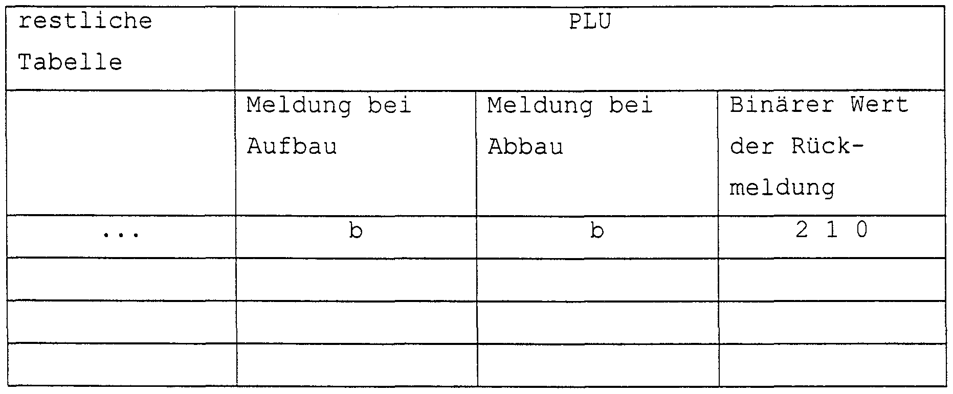
  • the routing tables can be expanded by a column that is used to send feedback messages to the loading logic when the connection specified in the relevant line is established or cleared down. In this way it can be specified in the column whether a feedback to the PLU should take place when the connection is established or terminated, and what type of feedback is.
  • the feedback occurs in accordance with DE 196 51 075.9-53 Figure 15, with a gate being used instead of the latch 1504, which switches through after setting either when connecting or disconnecting the connection and the feedback to the transistors (1502; Drivers are activated.
  • Fig. 1 shows a two-dimensional building block with cell array and nodes.
  • FIG. 2 shows a section from FIG. 1.
  • Fig. 3 shows several existing bus connections and the establishment of new connections.
  • Fig. 4 shows the establishment of new bus connections.
  • Fig. 5 shows the next step of establishing a connection.
  • Fig. 6 shows the collision of two buses.
  • Fig. 7 shows the gradual disconnection after a
  • Fig. 8 shows the gradual disconnection after a
  • Fig. 9 shows the gradual disconnection after a
  • Fig. 10 shows the gradual disconnection after a
  • Fig. 11 shows the re-establishment of the cleared connection after a certain period of time.
  • Fig. 12 shows the continuation of Fig. 6 when the node has more than one busbar and thus there is no collision.
  • Fig. 13 shows the connection of the bus segments with the
  • a node busbars A node busbars.
  • Fig. 14 shows the data transfer of a connection establishment.
  • Fig. 15 shows the data transfer of a disconnection.
  • 16 shows the control unit of a node.
  • Fig. 17 shows the broadcast to several data receivers.
  • FIG. 18 shows an improvement over FIG. 16
  • Control unit of a node with collision detectors Control unit of a node with collision detectors.
  • FIG. 19 shows an improvement over FIG. 16
  • Fig. 20 shows the busbars suitable for Fig. 18/19.
  • FIG. 21 shows an improved broadcasting to several nodes compared to FIG. 17.
  • Fig. 22 shows the flow control of Figs. 18-21.
  • FIG. 24 shows an optimized variant of FIG. 23.
  • 25 shows a data register with a synchronization unit.
  • Fig. 26 shows a collision detector after the extended one
  • Fig. 27 shows the control unit for Figs. 23-26.
  • Fig. 29 shows the control registers for Fig. 27 (2705).
  • FIG. 30 shows a bus structure using relative spatial coordinates in accordance with the extended routing method.
  • 31 shows a bus structure using absolute spatial coordinates in accordance with the extended routing method.
  • Figure 1 shows a block of the genera FPGA, DPGA, DFP (DE 44 16 881 AI).
  • the module is constructed two-dimensionally symmetrically from configurable cells (0101), 0101 can also represent a plurality of different configurable cells, which are combined into a group and networked with one another.
  • the nodes of the bus system (0102) are located between the cells. Several nodes are identified, which will establish several connections in the following exemplary embodiment.
  • Data transmitter A (0103) will subsequently establish a connection to data receiver A (0104), and data transmitter B (0106) with data receiver B (0105).
  • a partial enlargement (0107) is shown in FIG. 2.
  • Figure 2 shows a section of a block of the type described.
  • the configurable cell (s) of FIG. 1 (0101) are shown in 0201.
  • a bundle (0203) consisting of a large number of lines (the number is arbitrary and not exactly shown) connects 0201 to a node 0202.
  • the nodes (0202) are connected to one another via the bus segments (0205).
  • the nodes have bus segments 0206, the design of which is the same as that of bus segments 0205, to the nodes located outside of the enlargement.
  • the optional line bundle (0204) makes it clear that the configurable cell (s) can also be connected to a plurality of nodes (0202) via several different line bundles.
  • FIG. 3 shows the block at runtime. There are several connections:
  • the data transmitter A (0302) tries to establish a connection (0303) to the data receiver A (0307). However, the connection is rejected (REJECT) because it is blocked at node Z (0308). At the same time, data transmitter B (0304) establishes a bus segment (0305) to its receiver. This attempt succeeds because the addressed node and the required bus segment are not blocked.
  • FIG. 4 shows the next bus cycle.
  • the connections Y and Z have since been cleared.
  • the data transmitter A (0401) can now set up the bus segment (0403) because the node (0402) cannot more is blocked
  • FIG. 5 The bus structure started in FIG. 3 and continued via FIG. 4 continues in an equivalent manner to FIG. 4.
  • Figure 6 The connection establishment of the bus segment 0602 of the data transmitter B fails. Node 0601 is busy and delivers a REJECT signal to node 0603, which signals the failure of the connection establishment and causes the connection to be terminated.
  • Figure 7 shows the complete connection between the data transmitter A (0701) and the data receiver A (0702). The connection of the data transmitter B is further cleared down. Node 0703 supplies the REJECT signal to node 0705 via bus segment (0704). Segment 0704 is then removed.
  • Figure 8 The data transfer between data transmitter A and data receiver A begins. The connection of the data transmitter B is further cleared down. Node 0801 supplies the REJECT signal to node 0803 via bus segment (0802). Segment 0802 is then removed.
  • FIG. 9 The data transfer between data transmitter A and data receiver A continues. The last segment of data transmitter B is dismantled. The node 0901 delivers via the Bus segment (0902) the REJECT signal to node 0903. Segment 0902 is then removed.
  • Figure 10 The data transfer between data transmitter A and data receiver A continues.
  • the data transmitter B (1001) waits a period of time until it tries again to establish a connection to its data receiver.
  • Figure 11 shows the state several bus cycles later: The data transfer between the data transmitter A and the data receiver A is still taking place.
  • the data transmitter B (1101) starts a new attempt to establish a connection to its data receiver. It builds up a bus segment (1102) to the node (1103). If the connection of the data transmitter A to its data receiver A is terminated in the next bus cycles, the connection establishment of the data transmitter B (1101) succeeds, otherwise it fails again as brushed in FIG. 6.
  • FIG. 12 shows the continuation of FIG. 6 when the node 1202 is able to be set up as a connection, that is to say the node has several internal busbars. Therefore, the connection of the data transmitter A can be handled via the first busbar and the connection of the data transmitter B via the second.
  • the node 1202 sets up the bus segment 1203 to the data receiver B (1201).
  • FIG. 13 shows an internal network structure.
  • the busbars are switched to the bus segments west (1318), north (1316), east (1319), south (1317) via a group of gates (1308, 1309, 1310, 1311).
  • the busbars are connected to the O-REGl / 2 (see DE 196 51 075.9-53) via gates 1307 (1314, 1315).
  • the R-REG (see DE 196 51 075.9-53) is connected to the busbars via gates 1306.
  • the low-order and higher-order R-REG (1312, 1313) can be connected separately.
  • the gates are controlled via bus 1320.
  • the required gate system west, north, east, south
  • the internal busbar are specified.
  • FIG. 14a shows the establishment of a connection, the data transmitter (1401) transmitting the first data packet to the node of the data transmitter (1402).
  • Figure 14b The node selects from the routing table to rRDY rRDY is a status signal that indicates that
  • Data at the data transmitter are available (cf. DE 196 51 075.9-53) - - belonging entry.
  • the next bus segment is set up on the basis of this entry and the address of the routing table of the next node is transmitted.
  • Figure 14c The last node (1403), the data receiver node, receives the address for the entry within its routing table. The entry points to no further nodes, but to a cell. The node therefore immediately activates its gates to the selected cell.
  • FIG. 14d The data go directly to the receiver cell 1404 through the activated gate of 1403.
  • FIG. 14e The cell sends the oACK signal (cf. DE 196 51
  • the data transmitter will then send the next data packet in the next bus cycle (cf. FIG. 14e).
  • FIG. 15a There is a data connection from the data transmitter
  • FIG. 15b The data transmitter (1501) has ended its data transmission and sends an DISCONNECT signal to the first node.
  • the data receiver has been removed.
  • DISCONNECT line is looped through all nodes.
  • the DISCONNECT is propagated in one clock cycle; all
  • Figure 15g corresponds to Figure 15e.
  • Figure 16 shows the control of a node.
  • the requirements (1601) for establishing a connection come via the Priority decoder (1602) to the routing table (1603).
  • the priority decoder selects the request with the highest priority, whereby a request that has just failed is assigned the lowest priority.
  • the priority logic receives your requirements via status signals (e.g. those from the configurable cells (cf. DE 196 51 075.9-53) rRDY, oACK) or via the bus segments 1316, 1317, 1318, 1319.
  • status signals e.g. those from the configurable cells (cf. DE 196 51 075.9-53) rRDY, oACK) or via the bus segments 1316, 1317, 1318, 1319.
  • the data is interpreted by the priority logic as the address of the routing table and viewed as a request.
  • rRDY, oACK If status signals are present on the priority logic (rRDY, oACK), these are transferred to addresses for the routing table.
  • the addresses in the routing table select an entry.
  • the data of the entry (1604) are forwarded to a unit of AND gates (1605).
  • the binary number of the bus selection (BUS 1..0) is transmitted via a 2: 4 decoder (1606) in select signals.
  • the AND gate unit ANDs each signal with the same signal stored in a latch (1607). This means that the signal GATE1 of the routing table is rounded with the signal GATE1 of the latch, the signal GATE2 of the routing table with the signal GATE2 of the latch and so on.
  • the signals of the latch represent the status of the current network structure, ie the gates and busbars used are entered in the latch.
  • connection request If a connection of the connection request to the current state gives a true level, this means that the new connection request requires resources that are currently being used. All are via an OR gate (1608) AND gates linked together. If there is a true level at the output of the OR gate, the connection request is rejected (REJECT) (1609) because the required resources are occupied.
  • REJECT REJECT
  • the ACCEPT signal (1611) is generated from the REJECT signal via an inverter (1610).
  • the signals are forwarded to a state machine (1612), which can be implemented according to the prior art. This then controls the acceptance of the connection or the rejection. If the connection request is rejected, the state machine reports (1613) the REJECT to the priority decoder and the request receives the lowest priority.
  • the new status signals are ORED (1614) with the current status signals after the latch - the OR unit is constructed in the same way as the described AND unit (1605) and written back to the latch (1607).
  • the state machine controls via 1623 whether the OR unit (1614) or the mask (1616) is active.
  • the latch was killed by the state machine in 1622.
  • the new setting reaches the gates via bus 1615.
  • the subscription to a bus connection works in a similar way. However, the REJECT signal must occur when the resources are checked, since the bus connection that is to be cleared down must exist. Based on the REJECT, the state machine 1612 activates the mask 1616 instead of the OR unit 1614. The connection data of the connection to be terminated are masked out from the current network state and written back to the latch 1607. The state machine sends this before the new connection data is written back DISCONNECT signal to clear the connection to the next one
  • the control can access busbars 1301, 1302, 1303, 1304 directly via gates 1617, 1618, 1619, 1620.
  • the state machine can thus both transmit control signals (DISCONNECT) to the busbar and receive control signals from the busbar (REJECT, ACCEPT) and react to them. These gates also serve to transfer the entry position in the target table (over 1621) to the busbar.
  • the loading logic can access the routing table via 1624.
  • FIG. 17 shows a broadcasting of a data transmitter (1701) to a plurality of data receivers (1702) via a multiplicity of nodes
  • the bus is shown separated for clarity, namely in the acknowledgment line (ACK) (1703) and the rest of the bus
  • ACK is negated and delivered to the in turn inverting open collector bus driver. ACK is pulled high via a pull-up resistor 1705.
  • the circuit is designed so that the following cases occur:
  • H is present at the base of the transistor (1706). This means that the bus is pulled to L. If a result is broadcast to several data recipients, pull all nodes that have not yet acknowledged the result data and waiting cycles require the bus to be L. - If the corresponding bus is activated and the signal is acknowledged, L is present at the base of the transistor (1706). This means that the bus is not loaded. If a result is distributed to several data receivers by broadcasting, all nodes that have acknowledged the result data and do not require waiting cycles do not load the bus. Since the bus in its basic state assumes the H level, i.e. the acknowledgment, the non-acknowledgment according to case 2 overrides the acknowledgment by pulling the bus to L. The bus only goes to the H level, i.e. to the acknowledgment state, when all nodes involved in the connection acknowledge. A wired AND circuit is thus implemented.
  • Figure 18 shows the control of the busbar from Figure 13.
  • the logic is able to determine and allocate a free busbar itself.
  • One control unit 1801 is assigned to one busbar.
  • a control unit consists of a gate (1801a) to send the address information of the routing table to nodes connected to the busbar and a register (1801b), which takes over the control of the busbar.
  • 1801 receives the data from the routing table via the bus 1813 by means of a circuit described in FIG. 19.
  • the gates are unlocked via 1801b, which have access to the correspondingly assigned busbar.
  • Each gate has an activation signal to which an entry in 1801b is assigned. If no entry is set, the assigned busbar is unoccupied and can be freely assigned to an access request.
  • the check is carried out by an OR function (1802) via all enable signals to the gates.
  • the results of 1802 of all busbars are fed to an arbiter (1803) who selects one of the free busbars and responds to 1801 via an address bus (1804). If no busbar is free, 1803 signals this via 1805 to the controlling state machine.
  • Each entry in 1801b identifies a gate assigned to the busbar. The position is the same in every 1801b. That means from position p of a 1801b there is always the release signal for gate p, at position p + 1 that Release signal for gate p + 1 and at position q the release signal for gate q. If an OR function (1806) is executed for each gate p via the enable signals, the result indicates whether gate p is free or not.
  • An OR function (1811) is used to determine whether one of the gates is unlocked. Since all irrelevant gates are marked with "not activated", only the state of the gate required for the current connection establishment is forwarded to the state machine (1812). If the desired gate is unlocked, it cannot be used when the connection is currently being established, otherwise a collision would occur. The connection establishment is interrupted and either rejected or tried again at a later time.
  • FIG. 19 shows the arbiter for selecting the active bus and the routing table.
  • Each bus (2004, 2005, 2006) connected to a node sends its access request via a signal (1901) to an arbiter (1902), which selects one of the access requests.
  • the multiplexer (1904) is controlled via a decoder (1903) in such a way that either the number of the selected access (in the case of direct access through a configurable cell) (1905) or the lookup address of the selected one Access to the routing table 1906 is transmitted. 1906 outputs the data assigned to the value of 1905.
  • the lookup address for the next node is transmitted directly to 1801a via 1813.
  • the address of the next node is decoded (1907) via a mixer (1908), which is usually made up of OR gates, transmitted to 1801b by bus 1813. If the bus to the next node is set up, the activation of the gate to the previous node is made possible by connecting the address of the previous node, which is decoded via the decimal decoder 1909, to the bus 1813 in the mixer 1908 and transmitting it to 1801b.
  • Figure 20 shows the busbars (2001, 2002, 2003) for connecting the adjacent buses (2004, 2005, 2006).
  • the buses are connected to the busbars via the multiplexer / demultiplexer (2007) in accordance with the control by 1801b; the output signals p of all 1801b are fed to a multiplexer p, the output signals p + 1 of all 1801b, etc. to a multiplexer p + 1
  • Signals represent adjacent busbars, since each busbar controller controls exactly one (p) out of a multitude of signals (p x , p x + I, .., q x ). If a signal belonging to a busbar control is set, the corresponding busbar is activated by a 2007.
  • the timeout generators (2008) control the dismantling of the respective segment and the connected buses.
  • the timeout generators are taken directly from the routing table (1906) configured.
  • the connection is not shown in the drawings for the sake of simplicity.
  • the 1801a assigned to a respective busbar are connected to this busbar.
  • a bus segment (2105) is broadcast via a node (2101) to a plurality of nodes (2102, 2103, 2104).
  • the RDY handshake like the data, is sent directly to each recipient.
  • the retrograde ACK handshakes are switched to the OR gate (2107) and the AND gate (2108).
  • the masks are used to select which ACK is significant and whether the ACK is forwarded by a Boolean AND function or an OR function. Both functions are summarized via em OR gate (2109). If an ACK is irrelevant, mask 2105 passes a logical 0 (L level), while mask 2106 passes a logical 1 (H level).
  • the masks 2105 and 2106 are set separately from the routing table. The connection is not shown in the drawings for the sake of simplicity.
  • the basic state is "IDLE", which the status mechanism only leaves when a "request” (access) occurs AND a busbar AND the selected gate are free.
  • the state machine of the previous state machine acknowledges the bus structure by sending an ACK handshake.
  • the state machine goes into the SEND state, during which the data of the Routing table (via 1801a) are sent to the following routing table.
  • the state machine only leaves this state when an ACK handshake from the following routing table arrives OR when a "disconnect” signal arrives on the bus, for example by a timeout.
  • With a "disconnect” the status mechanism goes into the DISCONNECT state in order to disconnect the bus (this state is not necessary; in the implementation, the system jumps back directly to IDLE, but is used in this example for a better overview).
  • the system jumps back to the IDLE state; the gate of the previous routing table m 1801b is activated via 1909/1908.
  • the access data to be sent to the following routing table must be stored in 1801a during SEND, ie 1801a is a register; at the same time, the information about the previous routing table must be written with additional 1801b during SEND.
  • the arrival of the ACK handshake of the following routing table results in switching off 1801a and switching from the first 1801b to the second in independently constructed logic by storing the interconnection of the gate of the previous routing table.
  • FIG. 23 shows a node with the switching elements 1, 2, 3, 4, 5, 6 and the buses B1, B2, B3, B4.
  • FIG 23a The drawing is designed as a one-line system for better presentation. In fact, it is a bus system. All figures are to duplicate the amount of bus lines.
  • the switching elements are constructed from a transistor (2301).
  • Figure 23b) In order to be able to temporarily store data, the switching element is expanded by a register (2302). Via the transistors Tl, T2, T3, T4, the bidirectional buses Bn and Bm are switched to the register in such a way that either the transition Bm -> Bn or the transition Bn -> Bm is stored. Alternatively, bidirectional unsaved data transfer is made possible via T5.
  • the mode of the switching element is set as follows via the control signals S1, S2, S3, S4: Sl Bm -> Bn (unidirectional, saved)
  • FIG. 23d The inputs and outputs run on different lines (Bmi, Bmo, Bm, Bno) for better implementation in chips.
  • the drivers (2304) are unidirectional. There is no need to control the drivers.
  • FIG. 24 shows a node similar to the node from FIG. 23.
  • the advantage of the node is that it is easier to implement and manage the registers.
  • the drawing is designed as a one-line system for better presentation. In fact, it is a bus system. All figures are to duplicate the amount of bus lines.
  • the registers and drivers (A, B, C, D) are arranged upstream of the switching elements (1, 2, 3, 4, 5, 6). The switching elements are reduced to the cross connection shown in FIG. 24a.
  • the transistors T6, T7 are used to selectively switch the inputs (Imi, Ini) to the outputs (Imo, Ino) by means of the control lines S5, S6.
  • Figures 24b-d show different types of configurations of the registers and drivers (A, B, C, D).
  • a bidirectional bus is switched via T8 either as an input to regsiter 2401, or switched out of the output via T9, the node-internal bus Imo representing the signal source.
  • T8 and T9 are controlled via the control line S7.
  • the transistor pair T10 / T11 which is controlled via S8, a register bypass can be switched to enable the quasi-permanent mode.
  • the output of the register goes to the internal bus Imi.
  • the Imi and Imo are networked via the switching elements from FIG. 24a.
  • Figure 24c we have one instead of the transistor pair T8 / T9
  • Drivers 2403 are unidirectional, the control signal S7 is omitted.
  • FIG. 25 proposes a possible synchronization circuit for FIG. 24.
  • Registers 2401 for data storage are in
  • Register 2502 is used to store an RDY handshake signal, ie the information that there is valid data on the bus or in 2501. If there is no valid data in 2501, the output Q of 2502 is logic 0. If valid data arrives (RDY is active and logic 1), an enable signal (EN) is generated for registers 2501 and 2502 via AND gate 2503, the data and the RDY are saved with the rising clock edge. The input from 2503 for Q (from 2502) is inverting! If data arrives again, the output (Q) of 2502 is logic 1. The AND gate supplies a logic 0 and the registers are not enabled via EN. If the data is forwarded via the bus, the activation signal of the output driver (OE) is clear for
  • Figure 26 shows the test strategy to determine if a connection can be established, i.e. the network is free.
  • the status information of the switching elements 1, 2, 3, 4, 5, 6, which provides information as to whether a switching element is connected or free, is arranged in a matrix 2603.
  • the 90 ° switching elements 3, 4, 5, 6 form the corners, the 180 ° switching elements 1 and 2 the center pieces and occur twice.
  • the entire edge m which the switching element is located must be free. For example, it is possible to use 1 + 2, 6 + 4, 3 + 5. However, 6 + 2, 6 + 1, 2 + 5, 2 + 4, 2 + 3, etc. is impossible.
  • each edge is only occupied once.
  • the data for this is provided by register 2602, in which the current interconnection of the node is stored via input r; and the routing table 2601, which forwards the data of the desired new bus to the matrix via the input t.
  • the test circuit is shown in Figure 26a.
  • Each row (2605, 2606, 2607, 2608) is checked for the existence of an interconnection via e OR gates (2609, 2610, 2611, 2612). If there is an interconnected element m in the row, the respective OR gate supplies a logical 1. The result of the the respective row is linked by means of an AND gate to each of the new interconnections to be set up in the row. If the row is already occupied AND a further connection in the row is requested, the respective AND gate supplies a logical 1. The outputs of all AND gates are ORed (2613). The result of the test thus returns a logical 0 to 2604 if the requested networking is valid and a logical 1 if there is a collision.
  • the circuit in FIG. 26 is only able to process one request per unit of time.
  • a time optimization is shown in FIG. 27.
  • Access requests from the buses to the circuit go through 2701.
  • the routing table (2702) is not constructed from a conventional memory, but from a plurality of individual registers (2711). As a result, the data of all access requests can be read out simultaneously from the routing table via the multiplexers 2703.
  • the data for each access request is sent to a matrix (2704) according to FIG. 26, which receives the comparison data from the register with the current interconnection of the nodes (2705).
  • Circuit 2706 consists of an OR gate which determines the presence of a valid request to matrix 2704.
  • the result of 2704 is ANDed to the output of the OR gate via an inverter.
  • Each matrix has a circuit 2706.
  • the results of which are assigned to an arbiter 2707 switched, which selects one of the valid accesses.
  • the multiplexer 2708 is switched so that the data of the valid access reach the mixer 2709, which links the valid new access to the existing connection and forwards it to the register 2705 for storage.
  • This circuit is able to select exactly one valid from a set of 4 accesses.
  • a valid access can be processed from an arbitrarily adjustable number of requests.
  • lines 2801, 2805, 2802 and 2810 are used for this purpose, which lead to the additional circuit in FIG. 28 and allow a simultaneous selection of 2 accesses. If 2810 is wired, line 2710 is omitted. According to the principle presented below, any number of accesses can be selected at the same time by cascading.
  • the information as to which access was selected as "valid" is sent to the decoder 2803 via 2801.
  • the information is decoded in such a way that only the access data of the unselected access are passed to the matrices via the three multiplexers 2804. By eliminating the access already selected, the number of matrices is reduced by one.
  • the decoder works as shown in the table:
  • the table shows in the "Decoder” column the "valid" bus selected via 2802.
  • the MUX1-MUX3 columns indicate which bus the respective multiplexer selects, depending on the value 2802.
  • the matrices (2811), the logic (2806) and the arbiter (2807) operate as known from FIG.
  • the data of the access selected by the arbiter are passed to the mixer 2809 via the multiplexer 2808. Similar to the mixer 2709, it adds the data of the access selected by the logic of FIG. 28 to the output data of 2709 and passes the generated access data to the register 2705 via 2810.
  • the input data of the multiplexer 2808 must be transferred from their outputs due to the interconnection into the multiplexer 2804 be tapped.
  • FIG. 29 describes a register according to 2602 or 2705.
  • the outputs of mixers 2709 and 2809 are fed to the register as input data via 2901.
  • One register bank each 2902a / b manages one of the buses (Bl, B2, .. Bm) of the node.
  • the control of the node is stored in part a of a bank.
  • the timeout of the bus connection is defined in part b.
  • Part b consists of a loadable counter, the enable and reload of which is selected via the multiplexer 2903, adjustable by part a.
  • the reload and enable signals of the counter are generated as follows:
  • the register required for a reload i.e. the reloading of the meter, which contains the originally set meter reading is contained in 2902b.
  • 2904 tests for counter reading 0 to determine the timeout.
  • 2904 is only the figure in the figure Shown for understanding; the carry signal (ripple carry) of the counter is used in the implementation.
  • the transfer deletes the content of 2902a, which then passes on the status information "bus-free" and thus tears off the bus.
  • the signal BUS-DISCONNECT from the carry is switched to the bus and used to tear off the remaining bus segment.
  • BUS-RECONF is carried along with the data according to DE 197 04 728.9 and also causes the bus to be demolished if it occurs.
  • Both signals 2902 are supplied via OR gate 2905 and cause the register and counter to be cleared.
  • the timeout is deactivated by deactivating the enable signal in accordance with the tables listed above and loading the counter with a value greater than zero.
  • the data in the register are bus-oriented, not switching element-oriented. This data is sent to mixers 2709 and 2809 via 2906. Each control signal occurs m times (number of buses) and is designated in the notation Si, m , where m stands for the bus and i for the number of the switching element.
  • Figure 30 shows an example of two bus connections. Configurable elements or groups of configurable A node 3002 is assigned to elements (3001). Node 3003 transmits data to node 3004. The connection establishment is static. The node 3005 transmits the data dynamically to the destination node 3008. The segments 3006 and 3007 are occupied, so that the direction of travel changes in each case.
  • the X / Y space coordinates are specified in the nodes that are run through. Depending on the running direction, the coordinates are kept the same, increased or decreased by one. Based on the numerical value of the coordinates, the direction of travel and the destination can be identified.
  • the deviation of the direction of movement is calculated from the position (A, 3, C, D) of the incoming bus at the node and the sign of the (X / Y) movement.
  • Directions are used for the designation, with y forming the north-south axis and x forming the east-west axis:
  • the direction of travel and the direction of the sky of the incoming bus can be used to calculate which of the switching elements (1, 2, 3, 4, 5, 6) is addressed. Both of the above-mentioned calculations are trivial, so that the necessary calculation unit (XY2ADR) can be designed, for example, using lookup tables. Therefore, the calculation is not discussed further, but reference is made to the table shown above. The addressing in this example is relative.
  • Figure 31 shows the same example with absolute coordinates.
  • FIGS. 30 and 31 do not allow any deviation from the optimal direction. If, for example, segment 3009 in FIG. 30 were occupied, the data could not be transferred any further. It is possible to allow a deviation from the specified direction in the busy case. Then the connection could be established via 3010. However, the space for a possible deviation must be limited in order to avoid senseless routing attempts receive. A reasonable limit for deviations from the specified direction is +/- 1 to +/- 2.
  • FIGS. 32a and 32b show the necessary periphery around a node 3201 in order to evaluate or modify the spatial coordinates.
  • Figure 32a modifies relative coordinates according to their direction of travel. Subtract (3203) in the positive direction and add (3202) in the negative direction. The comparators (3204) check whether a coordinate has reached 0.
  • FIG. 32b compares absolute coordinates with the coordinates of the node, using the comparators 3205. In order to allow a deviation from the predetermined direction, the comparators 3205 and 3204 are expanded in such a way that they check and pass on the information as to whether a coordinate is in the deviation area (-Deviation ⁇ Kooromate ⁇ deviation). On the basis of this information, the calculation unit (XY2ADR) can modify the direction of movement within the limits of the permissible deviation and allow or prevent a deviation in the event of a collision of the predefined direction. This calculation is also trivial and can, if necessary, be carried out by expanding the lookup tables. In the table below, the maximum permissible deviation is indicated by A:
  • Figure 33 shows the behavior of a segmented bus.
  • the structure of the drawing corresponds to that already known.
  • a transmitter node Sa sends data to the receiver accounts Ea
  • another transmitter node Sb sends to Eb
  • a last one Sc to Ec which is also the receiver node Eb.
  • Collisions occur at segments 3301 and 3302.
  • all buses are quasi built up permanently; with the exception of segments 3301 and 3302.
  • These segments operate in the "Registered” mode and arbitrate one of the pending buses according to the set timeout.
  • the priority of the individual buses can be set via the respective timeout.
  • a relevant bus receives large "timeout rights", ie long cycles, while short cycles are available to an irrelevant bus.
  • FIGS. 23-27 only show the networking in the four directions.
  • a configurable cell or a group of configurable cells must also be added to a node.
  • the extensions required for this are shown in FIG. 34.
  • the identifications of the nodes correspond in FIG. 34a to FIG. 23 and in FIG. 34b to FIG. 24; the connection of the configurable elements is marked with Z.
  • the matrix 2603 is to be changed to 3401 according to FIG. 34c.
  • the interconnection is changed in accordance with FIG. 26.
  • Address lookup The address is not calculated, but generated by "looking up” in a memory.
  • ALU Arithmetic logical unit Basic unit for processing data.
  • the unit can perform arithmetic operations such as addition, subtraction, possibly also multiplication, division, series expansions etc.
  • the unit can be designed as an integer unit or as a floating point unit.
  • the unit can also perform logical operations such as AND, OR and comparisons.
  • Arbiter unit to distribute rights between signals.
  • Broadcast Send data from a PAE to several or all data receivers.
  • Bus request The request to establish a bus connection for data transfer. (Also connection request) Bus segment Section of a bus system between two
  • Bus states The way a bus works. There are two main states:
  • Quasi-permanent The bus behaves like a continuous one
  • the bus can only be used by one data packet (until its demolition).
  • a register is inserted between each segment, which delays the data by one clock cycle.
  • Each clock cycle (depending on the timeout) can be different
  • Data type Type of data characters, numbers, floating point numbers, signals (boolean), etc.
  • Decimal decoder Converts a binary signal into a decimal.
  • DFP data flow processor according to patent / disclosure DE 44 16 881
  • DISCONNECT Signal generated by timeout counters / generators for the demolition of a bus. Is routed to all nodes of a bus.
  • Gate group of transistors that perform a basic logic function are e.g. NAND, NOR, transmission gates.
  • Optimized for speed A bus system that is mostly quasi-permanent, has a high priority and is not influenced by other accesses.
  • Node element that connects several bus segments with each other and actively controls the connection establishment, but is passive during data transfer.
  • configurable element represents a unit of a logic module, which can be set by a configuration word for a special function.
  • Configurable elements are thus all types of RAM cells, multiplexers, arithmetic logic units, registers and all types of internal and external networking description etc.
  • configurable cell See logic cells Configuration Setting the function and networking of a logical unit, an (FPGA) cell or a PAE (see reconfigure).
  • Loading logic unit for configuring and reconfiguring the PAE. Designed by a microcontroller specially adapted to its task.
  • Latch memory element that normally passes a signal transparently during the H level and stores it during the L level. Latches are sometimes used in PAEs where the function of the level is exactly the opposite. Here, an inverter is switched before the clock of a conventional latch.
  • Logic cells Configurable cells used in DFPs, FPGAs, DPGAs that perform simple logic or arithmetic tasks according to their configuration.
  • LookUp table (LUT) Table that receives a value as an address and returns a result. For example, a number is given as an address and its sine is returned.
  • Mask A bit combination that specifies which signals from a source are forwarded and which signals are interrupted (masked out).
  • Mx unit for interconnecting multiple signals according to a specific mapping rule.
  • a logical operation usually takes place, or b) the signals are combined to form a bus, possibly c) several signal sources are selectively combined via several multiplexers.
  • Open collector circuit technology in which the collector of a transistor is connected to a bus signal that is pulled up to the H level by a pull-up.
  • the transistor emitter is at ground. If the transistor switches, the bus signal is pulled to the L level.
  • the advantage of the method is that a plurality of such transistors can control the bus without an electrical collision.
  • the signals are OR-linked, resulting in the so-called wired-OR.
  • PAE Processing Array Element EALU with O-REG, R-REG, R20-MUX, F-PLUREG, M-PLUREG, BM, SM, Sync, StateBack and Power UNIT.
  • Partner node Node with which a certain node has contact or wants to establish via a bus segment.
  • PLU unit for configuring and reconfiguring the PAE. Designed by a microcontroller specially adapted to its task.
  • Priority type The way in which a priority identifier is evaluated.
  • Priority decoder The signal with the highest priority is passed on or released.
  • Priority identifier Specifies the priority level (high to low) of a bus connection.
  • PullDown resistor that pulls a bus line onto a lever.
  • Source-optimized A bus system that is mostly registered and has low priorities to allow as many data senders (sources) as possible to access the bus.
  • RECONFIG Signal generated by configurable elements which indicates that the elements can be reconfigured and have ended their activity. Used to demolish all buses involved and lead to all nodes on a bus.
  • Register bank Combination of several registers with different sizes and functions into one group.
  • Register bypass line for bypassing a register, this deactivates the synchronization effect of the register.
  • Round-robin arbiter Arbiter that activates one signal at a time.
  • the currently activated signal has the lowest priority and is the last in the chain to be activated again.
  • the arbiter works in a circle.
  • Busbar on which several bus segments are brought together.
  • Schmitt trigger window comparator that uses a hysteresis to assign exactly one of two values to a signal, thereby improving the signal quality.
  • Switching table A switching table is a ring memory that is addressed by a controller.
  • the entries in a switching table can contain any configuration words.
  • the controller can execute commands.
  • the switching table reacts to trigger signals and reconfigures configurable elements based on an entry in a ring buffer.
  • Timeout generator Unit for generating a timeout according to different criteria, such as
  • Reconfiguration New configuration of any amount of PAEs while any remaining amount of PAEs continue their own functions (see configure).
  • State machine logic that can assume various states. The transitions between the states depend on different input parameters. These machines are used to control complex functions and correspond to the state of the art

Abstract

The invention relates to a bus system for DFPs DE 16 88 A1 and to building blocks with two dimensional or multidimensional programmable cell structures (of type FPGA, DPGA or the like), characterized in that a) the bus system comprises a plurality of electrically independent bus segments disconnected by nodes, b) the nodes actively connect or disconnect bus segments, whereby b1) several bus segments are joined and connected by gates to a bus bar located inside the node or b2) connection occurs directly via circuitry elements, drivers and/or registers, c) each node has a routing table where information on the structure of the connection is stored, d) each node has a monitoring unit, which verifies independently if a connection can be established or not.

Description

Internes Bussystem für DFPs, sowie Bausteinen mit zwei- oder mehrdimensionalen programmierbaren Zellstrukturen, zur Bewältigung großer Datenmengen mit hohem Vernetzungsaufwand.Internal bus system for DFPs, as well as modules with two- or multi-dimensional programmable cell structures, for handling large amounts of data with a high level of networking.
Hintergrund der Erfindung Stand der TechnikBackground of the Invention Prior Art
... in Systemen mit zwei- oder mehrdimensionalen programmierbaren Zellstrukturen (FPGAs, DPGAs) In FPGAs und DPGAs befinden sich interne Bussysteme, die entweder global Anschluß an alle oder eine große Menge von Logikzellen haben oder eine lokale NextNeighbour-Verbindung aufweisen. Beiden Arten ist gemeinsam, daß es sich um direkte Verbindungen zwischen zwei oder mehreren Logikzellen handelt. Weiterhin kann immer genau ein Signal den Bus benutzen, es sei denn, daß eine Multiplexerstruktur in eine Mehrzahl von Logikzellen zusammen mit einer Steuerung konfiguriert wird.... in systems with two- or multi-dimensional programmable cell structures (FPGAs, DPGAs) FPGAs and DPGAs contain internal bus systems that either have a global connection to all or a large number of logic cells or have a local NextNeighbour connection. Both types have in common that they are direct connections between two or more logic cells. Furthermore, exactly one signal can always use the bus, unless a multiplexer structure is configured in a plurality of logic cells together with a controller.
... in DFP-basierenden Systemen... in DFP-based systems
In DFP-basierenden Systemen, nach DE 44 16 881 existieren die selben bereits beschriebenen Bussysteme. Zusätzlich existiert die Möglichkeit ein Bussystem zu trennen, so daß mehrere getrennt nutzbare Teilbusse entstehen.In DFP-based systems, according to DE 44 16 881, the same bus systems already described exist. In addition, there is the option of separating a bus system, so that several separate sub-buses can be used.
... in IO-Bussysteme nach DE 196 54 595.1-53 In DE 196 54 595.1-53 wird ein IO-Bussystem beschrieben, das eine Vielzahl Bausteininterner Bussysteme, wobei ein Baustein ein FPGA, DPGA, DFP oder ähnlicher sein kann, zusammenfaßt und aus dem Baustein herausführt. Dabei können Speicherbaugruppen oder Peripherie oder weitere Bausteine oben genannter Gattung angesteuert werden. Es existiert nur ein Adressregister, bzw. ein Adresszähler um die externen Adressen zu generieren.... in IO bus systems according to DE 196 54 595.1-53 In DE 196 54 595.1-53 an IO bus system is described, which combines a large number of building block internal bus systems, one building block being an FPGA, DPGA, DFP or similar leads out of the block. Memory modules or peripherals or other modules of the type mentioned above can be controlled. There is only one address register or one address counter to generate the external addresses.
ProblemeProblems
Die üblichen Bussysteme sind nicht dazu geeigne große Datenmengen in Form von byteweise oder anders gruppierten Signalen zu übertragen. Besonders wenn die Bausteine zur Berechnung von Algorithmen verwendet werden ist es erforderlich, daß eine Vielzahl von Daten (paketen) gleichzeitig zwischen den einzelnen konfigurierten Funktionsbereichen eines Bausteines übertragen werden. In der üblichen Technik muß für jeden Datenpfad, das ist die Verbindung (der Bus) zweier (oder mehrerer) Funktionsblöcke, die dieselben Daten erhalten, eine direkte Punkt zu Punkt Verbindung aufgebaut werden, die dann ausschließlich den Datenverkehr zwischen eben diesen Funktionsblöcken regelt. Es kann sich immer genau ein Datenpaket auf dem Bus befinden. Der Vernetzungsaufwand wird extrem hoch. Die Geschwindigkeit: der heutigen internen Busse wird begrenzt durch die maximale Busbreite und die Laufzeit der Signale auf dem Bus. Beim in DE 196 54 595.1-53 beschriebenen IO-Bus kann pro 10- Zelle nur eine Art von Busverbindung aufgebaut werden, nämlich ausschließlich die in dem Adressregister programmierte. Es besteht keine Möglichkeit auf verschiedene Datentypen oder Datensender zu reagieren und diese mit verschiedenen externen Bausteinen zu verbinden. Verbesserung durch die Erfindung, AufgabeThe usual bus systems are not suitable for transferring large amounts of data in the form of byte-by-byte or other grouped signals. Especially when the modules are used to calculate algorithms, it is necessary that a large amount of data (packets) be transferred simultaneously between the individual configured functional areas of a module. In conventional technology, a direct point-to-point connection must be set up for each data path, i.e. the connection (the bus) of two (or more) function blocks that receive the same data, which then only regulates the data traffic between these function blocks. There can always be exactly one data packet on the bus. The networking effort is extremely high. The speed: today's internal buses are limited by the maximum bus width and the duration of the signals on the bus. In the IO bus described in DE 196 54 595.1-53, only one type of bus connection can be established per 10 cell, namely only the one programmed in the address register. There is no possibility to react to different data types or data transmitters and to connect them with different external blocks. Improvement by the invention, task
Ziel der Erfindung ist es, ein Bussystem zu schaffen, dasThe aim of the invention is to create a bus system that
Daten zwischen einer Vielzahl von Funktionsblöcken übertragen kann, wobei sich mehrere Datenpakete gleichzeitig auf dem Bus befinden können. Dabei erkennt das Bussystem für verschiedeneData can be transferred between a multitude of function blocks, whereby several data packets can be on the bus at the same time. The bus system recognizes for different
Datentypen oder Datensender automatisch die richtigeData types or data senders automatically the right one
Verbindung und baut diese auf.Connection and builds it up.
Die Einzelheiten und besondere Ausgestaltungen, sowie Merkmale des er indungsgemäßen Bussystems sind Gegenstand derThe details and special configurations, as well as features of the bus system according to the invention are the subject of
Patentansprüche .Claims.
Beschreibung der ErfindungDescription of the invention
Übersicht über die Erfindung, AbstraktOverview of the invention, abstract
Beschrieben wird ein Bussystem, das horizontal, vertikal, diagonal oder in jeder beliebigen Lage auf einem Baustein integriert werden kann.A bus system is described that can be integrated horizontally, vertically, diagonally or in any position on a module.
Das Bussystem ist in eine Vielzahl von Segmenten unterteilt, wobei die Trennung der Segmente durch eine Bussteuerschaltung erfolgt. Diese Bussteuerschaltung wird Knoten genannnt .The bus system is divided into a large number of segments, with the segments being separated by a bus control circuit. This bus control circuit is called a node.
Gleichzeitig übernimmt der Knoten das Routen, also das Steuern der Flußrichtung der Daten. Logikzellen oder PAE-Zellen nachAt the same time, the node takes over the routing, that is, the control of the flow direction of the data. Logic cells or PAE cells
DE 196 51 075.9-53 sind an die Knoten angeschlossen, sie senden und empfangen ihre Daten über die Knoten, wobei jedemDE 196 51 075.9-53 are connected to the nodes, they send and receive their data via the nodes, each
Datenpaket eine Zieladresse mitgegeben werden kann. Ebenfalls ist das Bussystem in der Lage über LookUp-Tabellen, imData packet can be given a destination address. The bus system is also capable of using LookUp tables in the
Folgende Routingtabellen genannt, Zieladressen zu generieren, hierzu kann vor allem das in DE 196 54 846.2-53 beschriebene Verfahren dienen. Die Bussysteme sind besonders zu einem direkten Anschluß an die in DE 196 54 595.1-53 beschriebenen INPUT-/OÜTPUT-CELLs geeignet. Das Auf- und Abbauen von Verbindungen, sowie die Synchronisation der Daten erfolgt automatisch. Schlägt ein Aufbau fehl, da das benötigte Bussegment momentan belegt ist, wird der Aufbau zu einem späteren Zeitpunkt wiederholt. Anhand unterschiedlicher Datentypen oder Datensender können automatisch unterschiedliche Verbindungen aufgebaut werden.The following routing tables are used to generate destination addresses, the method described in DE 196 54 846.2-53 can be used for this purpose. The bus systems are particularly suitable for direct connection to the INPUT- / OÜTPUT-CELLs described in DE 196 54 595.1-53. Connections are set up and cleared down and the data is synchronized automatically. If a setup fails because the required bus segment is currently occupied, the setup is repeated at a later time. Different connections can be established automatically using different data types or data transmitters.
Detailbeschreibung der Erfindung Das BussystemDetailed description of the invention The bus system
Auf einem Baustein befinden sich eine Vielzahl von Bussen, die horizontal, vertikal, diagonal oder in jeder beliebigen Lage auf dem Baustein angeordnet sind. Dabei sind die einzelnen Busse nicht durchgehend von einer Bausteinkante zur anderen, sondern sie sind in eine Mehrzahl von Bussegmenten unterteilt. Die Bussegmente werden durch die nachfolgend beschriebenen Knoten getrennt. Jedes Bussegment ist unabhängig von den anderen nutzbar und verschaltbar, wobei die Verschaltung von den Knoten übernommen wird. Auf dem Bussystem ist kann ein eigenes Protokoll implementiert sein, das von den Knoten verwaltet wird; ebenfalls ist denkbar, daß das Protokoll von den Zellen, die den Bus benutzen, verwaltet wird und die Knoten nur passive Schalter sind. Der KnotenThere is a large number of buses on a module, which are arranged horizontally, vertically, diagonally or in any position on the module. The individual buses are not continuous from one module edge to the other, but are divided into a plurality of bus segments. The bus segments are separated by the nodes described below. Each bus segment can be used and connected independently of the others, with the connection being taken over by the nodes. A separate protocol can be implemented on the bus system, which is managed by the nodes; it is also conceivable that the protocol is managed by the cells using the bus and the nodes are only passive switches. The knot
Ein Knoten dient der Verschaltung der einzelnen Bussegmente miteinander. Ebenfalls wird das Aufschalten der Zellen auf die Bussegmente von den Knoten übernommen.A node is used to interconnect the individual bus segments. The nodes are also responsible for connecting the cells to the bus segments.
In einem Knoten sind die Bussegmente aller Richtungen zusammengeführt, das bedeutet,The bus segments of all directions are brought together in a node, which means
- in einem zweidimensionalen System werden die Busse aus 4 Richtungen Norden (N) , Süden (S) , Osten (E) , Westen (W) auf den Knoten geführt.- In a two-dimensional system, the buses are led to the nodes from 4 directions north (N), south (S), east (E), west (W).
- in einem dreidimensionalen System werden die Busse aus 6 Richtungen Norden (N) , Süden (S) , Osten (E) , Westen (W) , Oben (T) , Unten (B) auf den Knoten geführt.- In a three-dimensional system, the buses are routed to the nodes from 6 directions north (N), south (S), east (E), west (W), top (T), bottom (B).
- in einem n-dimensionalen System werden die Busse aus n- Richtungen (je Dimension existiert ein Richtungsvektor dessen- In an n-dimensional system, the buses are from n directions (there is a direction vector of each dimension
Richtung durch das Vorzeichen bestimmt wird => pro Dimension existieren zwei Richtungen, die durch das Vorzeichen des Richtungsvektors unterschieden werden) auf den Knoten geführt.Direction is determined by the sign => there are two directions per dimension, which are distinguished by the sign of the direction vector) led to the node.
Knoten Typ AType A knot
Innerhalb des Knotens befindet sich ein Bussystem, auf das die externen Busse aufgeschaltet werden und das somit aus mehreren Sammelschienen besteht. Ein externer erster Bus wird über ein Tor auf eine Sa melschiene aufgeschaltet . Über ein weiteres Tor wird die Sammelschiene auf den externen zweiten Bus aufgeschaltet . Um Broadcasting, das Versenden von Daten an mehrere Empfänger, zu ermöglichen, können auch mehrere "zweite" Busse auf das interne Bussystem geschaltet werden. Die Tore können dabei als rein passive Schalter, als Bustreiber oder als Register/Latch ausgestaltet sein.There is a bus system inside the node, to which the external buses are connected and which thus consists of several busbars. An external first bus is connected to a busbar via a gate. The busbar is connected to the external second bus via another gate. In order to enable broadcasting, the sending of data to several receivers, several "second" buses can also be switched to the internal bus system. The gates can be designed as purely passive switches, as bus drivers or as registers / latches.
Weiterhin hat der Knoten Zugriff auf eine (oder mehrere) mit ihm verbundene (n) konfigurierbaren Elemente (Zellen). Diese verbindet er gegebenenfalls mit einem oder mehreren der angrenzenden Bussegmente.The node also has access to one (or more) configurable elements (cells) connected to it. If necessary, he connects these to one or more of the adjacent bus segments.
Knoten Typ BB type knot
Im Gegensatz zum Knoten Typ A existiert kein internes Bussystem. Der Knoten besteht aus n konfigurierbaren Schaltern, die jedes angrenzende Segment mit jedem anderen angrenzenden Segment verbinden können. Beispielsweise gilt bei 2-dimensionalen Strukturen n=6.In contrast to the type A node, there is no internal bus system. The node consists of n configurable switches that can connect any adjacent segment to any other adjacent segment. For example, for 2-dimensional structures, n = 6.
Figure imgf000008_0001
(N=Nord, 0=Ost, S=Süd, W=West](N = North, 0 = East, S = South, W = West]
Ein Schalter kann unidirektional oder bidirektional ausgestaltet sein, dabei kann er ein Register oder Latch zur Speicherung der Daten enthalten. Das "gewohnliche" RoutingverfahrenA switch can be unidirectional or bidirectional, it can contain a register or latch for storing the data. The "usual" routing procedure
Eine Verbindung wird initiiert von einem Datensender (DS) dies ist ein konfigurierbares Element (Logikzelle, BuszelleA connection is initiated by a data transmitter (DS) this is a configurable element (logic cell, bus cell
(auch Externe gemäß DE 196 54 595.1-53)) , der eine(also external according to DE 196 54 595.1-53)), the one
Verbindung zu einem Datenempfanger (DE) der ebenfalls aus einem konfigurierbaren Element besteht benotigt. Hierzu teilt der DS dem Knoten seine Busanforderung mit. Der erste Knoten direkt nach einem Datensender wird Initiator-Knoten genannt. Der entnimmt, wie nachfolgend beschrieben, einer internen Tabelle die Adresse des nächsten für den Datentransfers benotigten Knotens. Sofern der Knoten in der Lage ist, das erste benotigteConnection to a data receiver (DE) that also consists of a configurable element is required. To do this, the DS notifies the node of its bus request. The first node immediately after a data transmitter is called the initiator node. As described below, it takes the address of the next node required for data transfer from an internal table. If the knot is able, the first one needed
Bussegment anzusprechen das ist immer dann möglich, wenn das Bussegment UND eine interne Sammelschiene des Knoten frei st baut er die Verbindung auf, ansonsten weist er dieAddressing the bus segment is always possible if the bus segment AND an internal busbar of the node is free, it establishes the connection, otherwise it has the
Anforderung des DS zurück und der DS versucht den Zugriff zu einem spateren Zeitpunkt noch einmal, oder wartet und halt die Zugriffsanforderung weiter aufrecht, bis der Knoten sie aktzeptiert .Request the DS back and the DS tries the access again later, or waits and holds the access request until the node accepts it.
Jeder nachfolgende Knoten entnimmt wiederum die Aαresse des nächsten Knotens aus seiner internen Tabelle und setzt oen Aufbau der Verbindung fort. Ist der Knoten nicht in der Lage den Aufbau der Verbindung durchzufuhren (entweder ist das benotigte Bussegment besetzt oder die Sammelschiene des Knotens ist nicht frei) , so kann er entweder in einen Wartezustand springen, oder den Aufbau unterbrechen und einen Fehler an den Initiator-Knoten zurückmelden. Erst wenn eine Verbindung komplett aufgebaut ist, werden die Datenpakete übertragen und der Sender erhält erhält die Quittierungssignale für den Datenaustausch (vgl. rACK in DE 196 51 075.9-53). Dadurch wird der Datentransfer automatisch mit den Datensendern synchronistiert . Schlägt der Verbindungsaufbau fehl und muß er zu einem späteren Zeitpunkt wiederholt werden, erhält der Datensender kein Quittierungssignal, somit gehen keine Daten verloren.Each subsequent node in turn takes the address of the next node from its internal table and continues to set up the connection. If the node is not able to establish the connection (either the required bus segment is busy or the busbar of the node is not free), it can either jump to a wait state or interrupt the establishment and an error on the initiator node report back. Only when a connection is completely established, the data packets are transmitted and the transmitter receives the acknowledgment signals for the data exchange (cf. rACK in DE 196 51 075.9-53). This automatically synchronizes the data transfer with the data senders. If the connection fails and has to be repeated at a later time, the data transmitter does not receive an acknowledgment signal, so no data is lost.
Ist die Verbindung komplett aufgebaut, bleibt sie so lange quasi-permanent (das bedeutet, sie erscheint dem DS und DE wie eine direkte Verbindung) stehen, bis der DS die Verbindung durch eine Meldung an den Initiator-Knoten wieder auflöst. Es ist denkbar ein Timeout-Verfahren zu implementieren, das eine stehende Verbindung nach einer gewissen Zeit unterbricht, ins besondere dann, wenn längere Zeit kein Datentransfer stattgefunden hat, um die Bussegmente für andere Verbindungen freizugeben.Once the connection has been completely established, it remains quasi-permanent (this means that it appears to the DS and DE as a direct connection) until the DS breaks the connection again by sending a message to the initiator node. It is conceivable to implement a timeout method that interrupts a standing connection after a certain time, especially if there has been no data transfer for a long time in order to release the bus segments for other connections.
Das erweiterte RoutingverfahrenThe advanced routing process
Beim bisher beschriebenen Verbindungsaufbau befinden sich die Adressen nur während der Aufbauphase auf dem Bus. Während der Datenübertagen werden die Adressen nicht mehr übertragen. Beim Verfahren des erweiterten Verbindungsaufbaus laufen die Adressen ständig auf separaten Leitungen mit den Daten mit. Dabei existieren zwei Adressierungsschemata: 1. RaumkoordinatenWith the connection setup described so far, the addresses are only on the bus during the setup phase. The addresses are no longer transmitted during data transfer. When the extended connection is established, the addresses are always running with the data on separate lines. There are two addressing schemes: 1. Space coordinates
Als Adressen werden die Raumkoordinaten des Ziels angegeben. Die Raumkoordinaten sind von der gewählten Dimension des Systems abhängig. Beispielsweise benutzt ein 3-dimensionales System die Koordinaten X/Y/Z und ein 2-dimensionales X/Y. Prinzipiell ist das Verfahren auf ein beliebig dimensionales System anwendbar. Jeder Koordinate ist ein Richtungsvektor zugeordnet, der angibt, ob sich die Daten/der Verbindungsaufbau in positiver oder negativer Richtung bewegen/bewegt .The spatial coordinates of the destination are given as addresses. The spatial coordinates depend on the selected dimension of the system. For example, a 3-dimensional system uses the coordinates X / Y / Z and a 2-dimensional X / Y. In principle, the method can be applied to any system of any dimension. A direction vector is assigned to each coordinate, which indicates whether the data / the connection establishment moves / moves in a positive or negative direction.
Die Daten bewegen sich vom Ursprungsknoten in eine der eingestellten Richtungen. Dabei wird die entsprechende Richtungskoordinate beim Durchlauf eines Knotens so modifiziert, daßThe data moves from the origin node in one of the set directions. The corresponding direction coordinate is modified when passing through a node so that
- bei Bewegung in positiver Richtung 1 subtrahiert wird- Subtract 1 when moving in positive direction
- bei Bewegung in negativer Richtung 1 addiert wird- 1 is added when moving in the negative direction
Die Zielachse ist erreicht, wenn die Koordinate 0 ist, der Zielknoten ist erreicht, wenn alle Koordinaten 0 sind.The target axis is reached when the coordinate is 0, the target node is reached when all coordinates are 0.
Es ist implementierungsabhängig, ob ein zweier-Komplement generiert wird und eine Koordinate als negative Zahl dargestellt wird (auf die aufaddiert wird) oder ob von einer positiven Zahl subtrahiert wird. Ebenfalls kann auf eine positive Zahl so lange aufaddiert werden, bis ein Überlauf generiert wird, der die Zielposition kennzeichnet.It depends on the implementation whether a two's complement is generated and a coordinate is represented as a negative number (to which addition is made) or whether it is subtracted from a positive number. You can also add to a positive number until an overflow is generated that identifies the target position.
Es gibt zwei sinnvolle Strategien die Laufrichtung der Daten festzulegen: a. Statisches Verfahren: Die Daten laufen immer m dieselbe Richtung, d.h. es wird versucht immer die Richtung beizubehalten, so lange, bis ein Richtungswechsel unbedingt erforderlich ist. Ein Richtungswechsel ist erforderlich, wenn die aktuelle Richtungskoordinate gleich null ist, d.h. deren Zielposition erreicht wird.There are two sensible strategies to determine the direction of the data: a. Static procedure: The data always run in the same direction, ie an attempt is always made to maintain the direction until a change of direction is absolutely necessary. A change of direction is necessary if the current direction coordinate is zero, ie the target position is reached.
Wird die Zielposition einer Koordinate erreicht, werden die Daten in Richtung der Koordinaten bewegt, die ungleich 0 sind. Sind alle Koordinaten gleich null, ist der Zielknoten der Daten erreicht. b. Dynamisches Verfahren. Die Daten werden bel eoig in eine der möglichen Richtungen bewegt, ^obei die Bewegung immer in die vom Richtungsvektor vorgegebene Richtung erfolgt. Dabei bedeutet eine beliebige Bewegung, daß die Daten immer zu dem Knoten weitergeleitet werden, zu dem am wenigsten Verkehr herrscnt. Es wird also versucht immer den Weg der geringsten Kollisionen und Blockaden zu gehen. Dadurch kann das Verfahren u.U. schneller und bei großen Systemen geeigneter sein.If the target position of a coordinate is reached, the data is moved in the direction of the coordinates that are not equal to 0. If all coordinates are zero, the target node of the data has been reached. b. Dynamic process. The data is moved anywhere in one of the possible directions, while the movement is always in the direction specified by the direction vector. Any movement means that the data is always forwarded to the node with the least traffic. So it always tries to go the way of the smallest collisions and blockages. This may result in the procedure faster and more suitable for large systems.
2. Adress-Lookup2. Address lookup
Werden Lookup-Adressen übertragen, wird der jeweils nacnste Knoten in jedem Knoten neu bestimmt. D es geschieht indem m den nachfolgend beschriebenen Routingtabellen der Eintrag der Lookup-Adresse ausgelesen wird und so die Daten für das nächste Ziel festgelegt werden. Dieses Ablauf ist gleich wie im "gewohnlichen" Routing-Verfahren. Der Vorteil der Raumkoordinaten liegt darin, daß kein Lookup in einer Tabelle benötigt wird und somit weniger Verwaltungsaufwand anfällt.If lookup addresses are transmitted, the next node in each node is determined anew. D it is done by reading the entry of the lookup address in the routing tables described below and thus determining the data for the next destination. This process is the same as in the "usual" routing procedure. The advantage of the spatial coordinates is that no lookup in a table is required, which means less administrative work.
Der Vorteil des Adress-Lookup liegt in seiner Flexibilität und der genauen Vorhersagbarkeit der Verbindung.The advantage of the address lookup is its flexibility and the precise predictability of the connection.
Teilweise kann es sinnvoll beide Verfahren miteinander zu mischen. Dazu müssen beide Adressen (Raumkoordinaten undSometimes it can make sense to mix the two processes together. To do this, both addresses (spatial coordinates and
Lookup-Adressen) gleichzeitig übertragen werden.Lookup addresses) are transmitted simultaneously.
Sind die Raumkoordinaten nicht null, werden die Daten anhand der Raumkoordinaten übertragen. Sobald die Raumkoordinaten null erreichen, wird in der aktuellen Routingtabelle einIf the spatial coordinates are not zero, the data are transmitted using the spatial coordinates. As soon as the spatial coordinates reach zero, a will appear in the current routing table
Lookup an Stelle der Lookup-Adresse durchgeführt.Lookup performed in place of the lookup address.
Dadurch ist flexibel einstellbar über welchen Segmenten dieThis means that the segments can be flexibly adjusted
Daten per Lookup-Verfahren oder Raumkoordinaten-Verfahren übertragen werden.Data can be transferred using the lookup method or spatial coordinate method.
Die Buszustände des erweiterten Routingverfahrens 1. Quasi-permanentThe bus states of the extended routing procedure 1. Quasi-permanent
Eine Verbindung kann ähnlich zum "gewöhnlichen" Routingverfahren quasi-permanent aufgebaut werden. Dabei wird jeder Knoten, den ein erstes Datum durchläuft permanent gemäß den Adressen die die diesem Datum zugeordnet sind freigeschaltet. Die Freischaltung bleibt für alle nachfolgenden Daten so lange aufrechterhalten, bis ein Abbruch der Verbindung durchgeführt wird. Obwohl ein derartiger Aufbau im erweiterten Routingverfahren nicht zwingend notwendig ist, bietet er zwei Vorteile: i. Die Durchlaufzeit der Daten wird erheblich verringert. 11. Zeitverluste durch Arbitrierung werden vermieden.A connection can be established quasi-permanently, similar to the "normal" routing method. Every node that goes through a first date is permanently activated according to the addresses assigned to this date. The activation is maintained for all subsequent data until the connection is terminated. Although such a structure is not absolutely necessary in the extended routing method, it offers two advantages: i. The throughput time of the data is considerably reduced. 11. Time losses through arbitration are avoided.
2. Registered2. Registered
Dies ist der normale Buszustand. Eingehende Daten werden zunächst in einem Register zwischengespeichert. Beim Schreiben in das Register, wird ein Quittierungssignal an den sendenden Knoten geschickt. Daten werden nur in das Register geschrieben, wenn dieses leer ist, d.h. entweder vorher keine Daten m das Register geschrieben wurden oder die vorher geschriebenen Daten bereits weiterubertragen sind. Ist das Register nicht leer, wird so lange gewartet und kein Quittierungssignal erzeugt, bis das Register _eer ist. Die Register werden arbitriert und das Register mit der momentan αochsten Priorität wird übertragen. Die Arbitrierung und Übertragung findet zyklisch mit jedem Takt statt. Diese Methode eignet sich vor allem für Ubertragungskanale auf denen Daten vieler verschiedener Quellen zeitunkritisch übertragen werden müssen. Diese Methode wird quellenoptimiert genannt.This is the normal bus state. Incoming data are first stored in a register. When writing to the register, an acknowledgment signal is sent to the sending node. Data is only written to the register if it is empty, i.e. either no data has previously been written in the register or the previously written data has already been transferred. If the register is not empty, the system waits and no acknowledgment signal is generated until the register is _eer. The registers are arbitrated and the register with the currently highest priority is transferred. The arbitration and transmission takes place cyclically with every clock. This method is particularly suitable for transmission channels on which data from many different sources have to be transmitted in a time-uncritical manner. This method is called source-optimized.
3. Segmentiert3. Segmented
Ein segmentierter Ubertragungskanal besteht aus quasi- permanεnten und register-orientierten Knoten. Dabei ist der Ubertragungskanal stellenweise geschwmdigkeitsoptimiert quasipermanent und an anderen Stellen quellenoptimiert ausgestaltet . A segmented transmission channel consists of quasi-permanent and register-oriented nodes. In this case, the transmission channel is quasi-permanent in places optimized for speed and source-optimized in other places.
Die RoutingtabellenThe routing tables
Grundbaustein eines Knotens ist eine Routing-Tabelle, ähnlich der in DE 196 54 846.2-53 beschriebenen Switching-Tabellen.The basic building block of a node is a routing table, similar to the switching tables described in DE 196 54 846.2-53.
Der mögliche Aufbau einer solchen Tabelle ist wird anhand eines Ausführungsbeispieles beschrieben:The possible structure of such a table is described using an exemplary embodiment:
Figure imgf000015_0001
Jede Zeile stellt eine gültige Verbindung dar. Dabei können mehrere Verbindungen gleichzeitig aktiv sein, maximal so viel Verbindungen, wie freie interne Sammelschienen und freie externe Bussegmente existieren. Eine nachfolgend beschriebene Überwachungslogik übernimmt die Prüfung, ob eine neu ausgewählte Verbindung aufgebaut werden kann. Jede Zeile wird über ihre binare Adresse angesprochen und ausgewanlt. Weiterhin gibt es Sonderzeilen, die keine binare Adresse besitzen, sondern über Triggerssignale oder Zustandssignalen selektiert werden. Zu diesen Signalen gehören (vgl. DE 196 51 075.9-53)Each line represents a valid connection. Several connections can be active at the same time, maximum as many connections as there are free internal busbars and free external bus segments. The monitoring logic described below checks whether a newly selected connection can be established. Each line is addressed and selected via its binary address. There are also special lines that do not have a binary address, but are selected using trigger signals or status signals. These signals include (see DE 196 51 075.9-53)
- rRDYl, rRDYh- rRDYl, rRDYh
- oACKl, OÄCK2- oACKl, OÄCK2
Hierbei werden Busverbindungen zu den Datenempfangern (rRDY) automatisch immer dann aufgebaut, wenn die Datensender-Zelle gültige Ergebnisse besitzt. Bei den Signalen oACK ist der Empfanger-/Senderablauf vertauscht. Der Datenempfanger baut die Veroindung zu seinem Datensender auf, sobald der Datenempfanger seine Operanden abgearbeitet hat und m der Lage ist neue Operanden zu verarbeiten.Here, bus connections to the data receivers (rRDY) are automatically established whenever the data transmitter cell has valid results. In the case of the oACK signals, the receiver / transmitter sequence is reversed. The data receiver establishes the connection to its data transmitter as soon as the data receiver has processed its operands and is able to process new operands.
In den Spalten Tor werden die für die jeweilige Verbindung aktiven Tore eingetragen, dabei ist es möglich, daß nur ein Tor markiert ist und m den Spalten EALU eine Verbindung zu einem konfigurierbaren Element (einer oder mehrerer Zellen) zum Beispiel zu einem R-REG oder O-REG (vgl. DE 196 51 075.9- 53) gewählt wird.The gates that are active for the respective connection are entered in the Gate columns. It is possible that only one gate is marked and in the EALU columns a connection to a configurable element (one or more cells), for example to an R-REG or O-REG (cf. DE 196 51 075.9-53) is selected.
In der Spalte Bus wird die für diese Verbindung verwendete interne Sammelschiene ausgewählt, dabei ist der Wert binar, so daß in der beschriebenen Tabelle insgesamt 4 interne Sammelscheinen benutzt werden konnnen. Die Auswahl der internen Sammelschienen kann auch entfallen, m dem ein Prioritatsdekoder die erste freie Sammelschiene erkennt und diese automatisch zuteilt. In der Spalte Ein trag Posi tion in Ziel tabelle wird die Adresse der Zeile der Tabelle angegeben, die den Knoten steuert, zu dem Verbindung aufgenommen wird. An dieser Adresse stehen die für die aktuelle Verbindung benötigten Routinginformationen im nächsten Knoten.The internal busbar used for this connection is selected in the Bus column. The value is binary, so that a total of 4 internal busbars can be used in the table described. The selection of the internal busbars can also be omitted if a priority decoder recognizes the first free busbar and assigns it automatically. In the column Entry position in target table the address of the row of the table is specified which controls the node to which the connection is established. The routing information required for the current connection is in the next node at this address.
Die Spalte Laufzei t ist optional. Darin kann die erwartete Signallaufzeit vom DS zum DE angegeben werden. Diese Information kann für Berechungen des Datendurchsatzes oder zur Generierung eines Timeout verwendet werden.The column runtime is optional. It can be used to specify the expected signal transit time from DS to DE. This information can be used to calculate data throughput or to generate a timeout.
Die Spalte Aufba uzei t ist optional. Darin kann die maximale Zeit zum Aufbauen der Verbindung zum nächsten Knoten (oder der gesamten Verbindung vom DS zum DE) angegeben werden. Wird diese Zeit überschritten kann über einen Timeout der Verbindungsaufbau abgebrochen werden und die Bussegmente und Knoten werden für andere Verbindungen frei. Zu einem späteren Zeitpunkt versucht der DS erneut die Verbindung herzustellen.The Construction time column is optional. The maximum time for establishing the connection to the next node (or the entire connection from the DS to the DE) can be specified in this. If this time is exceeded, the connection establishment can be terminated via a timeout and the bus segments and nodes become free for other connections. At a later time, the DS tries to connect again.
Die Einträge in der Routingtabelle können gemäß bekannten Verfahren (DE 196 51 075.9-53, DE 196 54 846.2-53) von einer Ladelogik konfiguriert und umkonfiguriert werden.The entries in the routing table can be configured and reconfigured by a loading logic in accordance with known methods (DE 196 51 075.9-53, DE 196 54 846.2-53).
Wird das "erweiterte" Routingverfahren verwendet, müssen die Raumkoordinaten den Routingtabellen hinzugefügt werden. Ebenfalls wird eine Priori tä tskennung erwartet. Die Priori tä tskennung gibt Auskunft, wie relevant ein Kanal für die Leistung eines Bausteines ist. Ist die Prioritätskennung sehr hoch, steigt die Relevanz des Kanales. Dabei kann die Kennung auf drei Arten ausgelegt werden:If the "extended" routing method is used, the spatial coordinates must be added to the routing tables. Priority identification is also expected. The priority identifier provides information on how relevant a channel is for the performance of a module. If the priority identifier is very high, the relevance of the channel increases. The identifier can be interpreted in three ways:
1. Timeout1. Timeout
Die Kennung gibt an, nach wievielen ungenutzten Taktzyklen der Kanal abgerissen werden soll, also nach wievielen Zyklen eine DISCONNECT generiert wird.The identifier indicates after how many unused clock cycles the channel is to be torn down, i.e. after how many cycles a DISCONNECT is generated.
2. Paket-Größe2. Package size
Die Kennung gibt an, nach wievielen Datenpaketen ein DISCONNECT generiert wird.The identifier specifies the number of data packets after which a DISCONNECT is generated.
3. Takt-Zyklen3. Clock cycles
Die Kennung gibt an, nach wievielen Taktzyklen ein DISCONNECT generiert wird.The identifier indicates the number of clock cycles after which a DISCONNECT is generated.
Dabei kann fest eine der 3 möglichen Arten implementiert werden, oder mittels einer zusätzlichen Angabe eine Art ausgewählt werden.One of the 3 possible types can be implemented, or a type can be selected by means of additional information.
Die Prioritätsart { Prioart in der nachstehenden Tabelle) wird in der nachfolgen beispielsweise aufgeführten Routingtabelle wie folgt ausgewertet:The priority type (priority type in the table below) is evaluated in the following routing table, for example:
Figure imgf000018_0001
Permanent kann auch dargestellt werden, indem ein Wert der Priori tä tskennung fest als "permanent" vorgegeben ist. Dafür eignet sich für gewöhnlich besonders der Maximalwert der Priori tä tskennung oder null.
Figure imgf000018_0001
Permanent can also be represented by a value of the priority identifier being fixed as "permanent". The maximum value of the priority identifier or zero is usually particularly suitable for this.
Figure imgf000019_0001
Der ArbiterThe arbiter
Der Routingtabelle vorgeschaltet ist ein Arbiter, die aus der Menge der Anfragen zum Verbindungsaufbau über die Routingtabelle einige Signale auswählt. Dabei ist es sinnvoll den Arbiter aus einem gewöhnlichen Priority-Logik und einem sogenannten Round-Robin-Arbiter nach dem Stand der Technik (er schaltet die höchste Priorität auf einer Zeitscheibe immer dem nächsten Signal zu, das bedeutet, das Signal, das momentan die höchste Priorität hat, wird als nächstes die Niederste besitzen und dann mit jedem Zugriff eine Höhere erhalten) aufzubauen. Dabei kann die Priority-Logik dazu dienen einigen Signalen, wie zum Beispiel rACK, oRDY grundsätzlich eine besonders hohe oder besonders niedere Priorität zuzuordnen. Der Round-Robm-Arbiter sorgt dafür, daß ein angeforderter Verbindungsaufbau, der soeben nicht aufbaubar war, die niederste Priorität erhalt und somit wartet, bis alle anderen Verbindungsanforderungen entweder aufgebaut oder überprüft wurden.An upstream of the routing table is an arbiter, which selects some signals from the set of requests to establish a connection via the routing table. It makes sense to use the arbiter consisting of a conventional priority logic and a so-called round robin arbiter according to the prior art (it always switches the highest priority on a time slice to the next signal, which means the signal that is currently the highest Priority, will have the lowest next and then get a higher one with each access). The priority logic can serve some Always assign signals such as rACK, oRDY to a particularly high or particularly low priority. The round-robm arbiter ensures that a requested connection establishment, which has not just been established, receives the lowest priority and thus waits until all other connection requests have either been established or checked.
Die Zustandsmaschme (Steuerung)The state machine (control)
Eine Zustandsmaschme steuert die internen Ablaufe im Knoten.A state machine controls the internal processes in the node.
Dabei ist die Zustandsmsch e zweigeteilt:The state structure is divided into two:
- Die Steuerung des Knotens- The control of the node
- Die Steuerung des Bustransfers und der Synchronistation. Dabei kann auf eine Zustandsmaschme ähnlich der m DE 196 51 075.9-53 beschriebenen zurückgegriffen werden.- The control of the bus transfer and the synchronization. A state machine similar to that described in DE 196 51 075.9-53 can be used.
Die Zustandsmaschme (n) sind gemäß dem Stand der Technik implementierbar und werden nicht nahers beschrieben.The state machine (s) can be implemented in accordance with the prior art and are not described in more detail.
Die UberwachungsemheitThe surveillance unit
Eine Uberwachungsemheit ist der Routingtabelle nachgeschaltet. Sie entnimmt die m eine adressierte Zeile eingetragenen Daten und überprüft ob der Verbindungsaufbau möglich ist.A monitoring unit is placed after the routing table. It takes the data from an addressed line and checks whether the connection can be established.
Dabei werden vor allem folgende Punkte überprüft:The following points in particular are checked:
- Steht eine freie interne Sammelschiene zur Verfugung.- A free internal busbar is available.
- Ist das angeforderte Tor frei. - Ist das angeforderte externe Bussegment frei.- The requested gate is free. - Is the requested external bus segment free?
a) Ist die Überprüfung positiv, wird das Signal ACCEPT generiert und an die Zustandsmaschinen, sowie die, den Verbindungsaufbau anfordernde Einheit, gesendet, um einen erfolgreichen Aufbau zu signalisieren. b) Ist die Überprüfung negativ, wird das Signal REJECT generiert und an die Zustandsmaschinen, sowie die, den Verbindungsaufbau anfordernde Einheit, gesendet, um einen fehlgeschlagenen Aufbau zu signalisieren. Auf dieses Signal kann der oben beschriebene Arbiter reagieren und die Priorität dieser Anforderung auf die Niederste setzen.a) If the check is positive, the signal ACCEPT is generated and sent to the state machines and to the unit requesting the connection to signal a successful establishment. b) If the check is negative, the REJECT signal is generated and sent to the state machines and to the unit requesting the connection to signal a failed setup. The arbiter described above can react to this signal and set the priority of this request to the lowest.
VerbindungsabbauDisconnection
Eine bestehende Verbindung kann durch verschiedene Kriterien wieder abgebaut werden. Zu den wichtigsten Kriterien zählen: Timeout: Eine Verbindung wird abgebaut, da über eine längere Zeitspanne kein Datentransfer stattgefunden hat. Ein Timeout kann einfach über einen ladbaren Abwärtszähler implementiert werden. Der Zähler wird bei jedem übertragenen Datum neu mit einem festen Ausgangswert, der die Zeitspannne bis zum Timeout repräsentiert, geladen. Findet kein Datentransfer statt, zählt er mit jedem Bustakt um eins herunter. Kommt er bei null an, ist die maximale Zeitspanne abgelaufen und der Bus wird abgebaut .An existing connection can be cleared down using various criteria. The most important criteria include: Timeout: A connection is cleared down because no data transfer has taken place over a longer period of time. A timeout can easily be implemented using a loadable down counter. The counter is reloaded with each transmitted date with a fixed output value that represents the time span until the timeout. If there is no data transfer, it counts down by one with every bus cycle. If it arrives at zero, the maximum time has expired and the bus is dismantled.
Datenzähler: Ein ladbarer Zähler wird mit der zu übertragenden Anzahl von Daten geladen. Bei jedem Datentransfer zählt der Zähler um eins herab. Kommt der Zähler bei null an, sind alle Daten übertragen und der Bus wird abgebaut.Data counter: A loadable counter is loaded with the number of data to be transferred. With every data transfer the counts Counter down by one. If the counter arrives at zero, all data is transferred and the bus is dismantled.
Synchronisationssignale (vgl. DE 197 04 728.9, RECONFIG) : Der Busabbau wird durch die Status- und/oder Synchronisationssignale der Zelle (n) gesteuert, die als Datensender auftreten. Zeigen die Zellen beispielweise an, daß ihre Datenverarbeitung beendet ist oder daß sie umkonfiguriert werden können, wird der Bus abgebaut, da er nicht mehr benötigt wird. Zu diesen Signalen gehören auch rRDY, oACK.Synchronization signals (cf. DE 197 04 728.9, RECONFIG): The bus breakdown is controlled by the status and / or synchronization signals of the cell (s) that occur as data transmitters. If the cells indicate, for example, that their data processing has ended or that they can be reconfigured, the bus is dismantled because it is no longer required. These signals also include rRDY, oACK.
Der Verbindungsabbau geht dabei so vonstatten, daß vom Initiator-Knoten aus ein Signal zum Abbauen der Verbindung gesendet wird Jeder weitere Knoten sendet das empfangene Signal an seine (n) Partnerknoten weiter und löst die Verbindung sofort auf.The termination of the connection takes place in such a way that a signal for clearing the connection is sent from the initiator node. Each further node transmits the received signal to its partner node (s) and immediately dissolves the connection.
Im erweiterten Routingverfahren werden quasi-permanente Busse entweder durch das RECONFIG-Synchronisationssignal (vgl. DE 197 04 728.9) oder gemäß der Prioritätskennung abgebaut. Wird das Ende einer Verbindung gemäß der Prioritätskennung von einem Knoten festgestellt, wird von ihm das DISCONNECT-Signal zum Abbruch des Busses generiert und an alle anderen Knoten weitergeleitet. Die Knoten reagieren auf ein DISCONNECT wie auf ein RECONFIG.In the extended routing method, quasi-permanent buses are either reduced by the RECONFIG synchronization signal (cf. DE 197 04 728.9) or according to the priority identifier. If the end of a connection is determined by a node according to the priority identifier, it generates the DISCONNECT signal for breaking the bus and forwards it to all other nodes. The nodes react to a DISCONNECT like to a RECONFIG.
Bei register-orientierten Knoten ist ein Verbindungsabbau nicht notwendig, da eine Verbindung dynamisch mit den eintreffenden Daten gemäß der zugeordneten Adressen aufgebaut wird. Nach dem Weiterleiten der Daten ist die Verbindung automatisch abgebaut und für andere Übertragungen frei. BroadcastingWith register-oriented nodes, it is not necessary to clear the connection, since a connection is established dynamically with the incoming data in accordance with the assigned addresses. After the data has been forwarded, the connection is automatically terminated and free for other transmissions. Broadcasting
In DE 196 51 075.9-53 ist ein Bussystem beschrieben, das das Senden eines Datenpaketes an mehrere Empfänger erlaubt und ebenfalls eine Quittierung des Datentransfers ermöglicht. Dasselbe System kann bei dem hier beschriebenen Verfahren verwendet werden. Es ist ohne weiteres möglich, mehrere Tore auf eine Sammelschiene zu schalten. Dabei wird nur eine Zeile in der Routingtabelle verwendet. Die Adresse innerhalb der Zielroutingtabellen Eintrag Posi tion in Ziel tabelle muß dabei bei jeder der selektierten Routingtabellen zwangsläufig dieselbe sein.DE 196 51 075.9-53 describes a bus system that allows a data packet to be sent to several receivers and also enables the data transfer to be acknowledged. The same system can be used in the method described here. It is easily possible to connect several gates to one busbar. Only one line is used in the routing table. The address in the destination routing table entry Position in destination table must necessarily be the same for each of the selected routing tables.
Um dieses Problem zu umgehen, ist es möglich mehrere Einträge für als Eintrag Posi tion in Ziel tabelle zur Verfügung zu stellen. Beispielsweise könnte für jedes Tor ein separater Eintrag Posi tion in Ziel tabelle existieren. Damit ist jedem Tor eine Adresse innerhalb der Zielroutingtabelle zugeordnet.To avoid this problem, it is possible to provide several entries for the entry position in the target table. For example, there could be a separate entry in the target table for each gate. This means that each gate is assigned an address within the target routing table.
Die Quittierung erfolgt genau wie in DE 196 51 075.9-53 beschrieben über Signalleitungen, die von Open-Kollektor- Treiber getrieben werden und mit einem Transistor abgeschlossen sind.The acknowledgment takes place exactly as described in DE 196 51 075.9-53 via signal lines which are driven by open collector drivers and are terminated with a transistor.
Um eine bessere Implementierbarkeit in existierende Chip- Technologien zu ermöglichen können Quittierungssignale in einem Knoten zunächst maskiert und danach logisch miteinander verknüpft werden. Die logische Verknüpfung wird an den nächsten Knoten weitergeleitet. Findet beispielsweise in allen durchlaufenden Knoten eine logische UND-Verknupfung der Quittierungssignale statt, ist das Resultat dasselbe, wie bei einer Open-Kollektor-Schaltung.In order to enable better implementation in existing chip technologies, acknowledgment signals can first be masked in a node and then logically linked to one another. The logical link is forwarded to the next node. For example, found in all the nodes that pass through a logical AND operation of the acknowledgment signals, the result is the same as with an open collector circuit.
Ladelogik (PLU)Charge logic (PLU)
Eine Ladelogik im Sinne von DE 44 16 881 AI ist an dieA loading logic in the sense of DE 44 16 881 AI is to the
Routingtabelle angeschlossen. Über diese kann dieRouting table connected. Via this the
Routingtabelle äquivalent zu den Switchmgtabellen aus DERouting table equivalent to the switchmgtables from DE
196 54 846.2-53 konfiguriert und umkonfiguriert werden.196 54 846.2-53 configured and reconfigured.
Die Routingtabellen können um eine Spalte erweitert werden, die benutzt wird um Ruckmeldungen an die Ladelogik zu senden, wenn die in der betreffenden Zeile angegebene Verbindung auf- oder abgebaut wird. So kann in der Spalte angegeoen werden, ob eine Ruckmeldung an die PLU erfolgen soll, wenn αie Verbindung auf- oder abgebaut wird, sowie welcher Art die Rückmeldung ist. Die Ruckmeldung erfolgt gemäß DE 196 51 075.9-53 Figur 15, wobei statt des Latches 1504 ein Tor eingesetzt ist, das e nach Einstellung entweder beim Verbmdungsaufoau oder - abbau durchschaltet und die Ruckmeldung an die Transistoren (1502;, die als Open-Kollektor-Treiber geschaltet sind ansteuern. The routing tables can be expanded by a column that is used to send feedback messages to the loading logic when the connection specified in the relevant line is established or cleared down. In this way it can be specified in the column whether a feedback to the PLU should take place when the connection is established or terminated, and what type of feedback is. The feedback occurs in accordance with DE 196 51 075.9-53 Figure 15, with a gate being used instead of the latch 1504, which switches through after setting either when connecting or disconnecting the connection and the feedback to the transistors (1502; Drivers are activated.
Figure imgf000025_0001
Kurzbeschreibung der DiagrammeBrief description of the diagrams
Fig. 1 Zeigt einen zweisimensionalen Baustein mit Zellarray und Knoten.Fig. 1 shows a two-dimensional building block with cell array and nodes.
Fig. 2 Zeigt einen Ausschnitt aus Fig. 1.FIG. 2 shows a section from FIG. 1.
Fig. 3 Zeigt mehrere bestehende Busverbindungen und den Aufbau neuer Verbindungen.Fig. 3 shows several existing bus connections and the establishment of new connections.
Fig. 4 Zeigt den Aufbau neuer Busverbindungen.Fig. 4 shows the establishment of new bus connections.
Fig. 5 Zeigt den nächsten Schritt des Verbindungsaufbaus .Fig. 5 shows the next step of establishing a connection.
Fig. 6 Zeigt die Kollistion zweier Busse.Fig. 6 shows the collision of two buses.
Fig. 7 Zeigt den schrittweisen Verbindungsabbau nach einerFig. 7 shows the gradual disconnection after a
Kollision.Collision.
Fig. 8 Zeigt den schrittweisen Verbindungsabbau nach einerFig. 8 shows the gradual disconnection after a
Kollision.Collision.
Fig. 9 Zeigt den schrittweisen Verbindungsabbau nach einerFig. 9 shows the gradual disconnection after a
Kollision.Collision.
Fig. 10 Zeigt den schrittweisen Verbindungsabbau nach einerFig. 10 shows the gradual disconnection after a
Kollision. Fig. 11 Zeigt den Neuaufbau der abgebauten Verbindung nach einer gewissen Zeitspanne.Collision. Fig. 11 shows the re-establishment of the cleared connection after a certain period of time.
Fig. 12 Zeigt d e Fortsetzung von Fig. 6, wenn der Knoten mehr als eine Sammelschiene Desitzt und somit keine Kollision stattfindet .Fig. 12 shows the continuation of Fig. 6 when the node has more than one busbar and thus there is no collision.
Fig. 13 Zeigt die Verbindung der Bussegmente mit denFig. 13 shows the connection of the bus segments with the
Sammelschienen eines Knotens.A node busbars.
Fig. 14 Zeigt den Datentransfer eines Verbindungsaufbaus. DieFig. 14 shows the data transfer of a connection establishment. The
Unterfiguren zeigen den Zustand der Verbindung jeweils imSub-figures show the state of the connection in each case
Abstanden von einem Buszyklus.Distances from a bus cycle.
Fig. 15 Zeigt den Datentransfer eines Verbindungsabbaus. DieFig. 15 shows the data transfer of a disconnection. The
Unterfiguren zeigen den Zustand der Verbindung jeweils imSub-figures show the state of the connection in each case
Abstanden von einem Buszyklus.Distances from a bus cycle.
Fig. 16 zeigt die Steuereinheit eines Knotens.16 shows the control unit of a node.
Fig. 17 Zeigt das Broadcastmg an mehrere Datenempfanger .Fig. 17 shows the broadcast to several data receivers.
Fig. 18 zeigt eine gegenüber Figur 16 verbesserteFIG. 18 shows an improvement over FIG. 16
Steuereinneit eines Knoten mit Kollisionsdetektoren .Control unit of a node with collision detectors.
Fig. 19 zeigt eine gegenüber Fig. 16 verbesserteFIG. 19 shows an improvement over FIG. 16
Routingtabelle mit Ansteuerung der Fig. 18.Routing table with control of FIG. 18.
Fig. 20 zeigt die zu Fig. 18/19 passenden Sammelschienen.Fig. 20 shows the busbars suitable for Fig. 18/19.
Fig. 21 zeigt e gegenüber Fig. 17 verbessertes Broadcastmg an mehrere Knoten.FIG. 21 shows an improved broadcasting to several nodes compared to FIG. 17.
Fig. 22 zeigt die Ablaufsteuerung der Fig. 18-21.Fig. 22 shows the flow control of Figs. 18-21.
Fig. 23 zeigt einen Busknoten gemäß dem erweiterten23 shows a bus node according to the extended one
Routingverfahren .Routing method.
Fig. 24 zeigt eine optimierte Variante von Fig. 23.24 shows an optimized variant of FIG. 23.
Fig. 25 zeigt em Datenregister mit Synchronisationseinheit.25 shows a data register with a synchronization unit.
Fig. 26 zeigt einen Kollisionsdetektor nach dem erweitertenFig. 26 shows a collision detector after the extended one
Routingverfahren . Fig. 27 zeigt die Steuereinheit für Fig. 23-26.Routing method. Fig. 27 shows the control unit for Figs. 23-26.
Fig. 28 zeigt einen durchsatzsteigernden, kaskadierbaren28 shows a throughput-increasing, cascadable
Zusatz zu Fig. 27.Addition to Fig. 27.
Fig. 29 zeigt die Steuerregister für Fig. 27 (2705) .Fig. 29 shows the control registers for Fig. 27 (2705).
Fig. 30 zeigt einen Busaufbau über relative Raumkoordinaten gemäß dem erweiterten Routingverfahren.30 shows a bus structure using relative spatial coordinates in accordance with the extended routing method.
Fig. 31 zeigt einen Busaufbau über absolute Raumkoordinaten gemäß dem erweiterten Routingverfahren.31 shows a bus structure using absolute spatial coordinates in accordance with the extended routing method.
Fig. 32 zeigt die Verwaltung der Raumkoordinaten.32 shows the management of the spatial coordinates.
Fig. 33 zeigt einen segmentierten Busaufbau.33 shows a segmented bus structure.
Detailbeschreibung der DiagrammeDetailed description of the diagrams
Figur 1 zeigt einen Baustein der Gattungen FPGA, DPGA, DFP (DE 44 16 881 AI) . Der Baustein ist zweidimensional symmetrisch aus konfigurierbaren Zellen (0101) aufgebaut, dabei kann 0101 auch eine Mehrzahl von auch unterschiedlichen konfigurierbaren Zellen, die zu einer Gruppe zusammengefaßt und untereinander vernetzt sind, repräsentieren. Zwischen den Zellen befinden sich die Knoten des Bussystemes (0102). Dabei sind mehrere Knoten gekennzeichnet, die im folgenden Ausführungsbeispiel mehrere Verbindugnen aufbauen werden. Der Datensender A (0103) wird im Folgenden eine Verbindung zum Datenempfänger A (0104) aufbauen, sowie der Datensender B (0106) mit dem Datenempfänger B (0105) . Eine ausschnittsweise Vergrößerung (0107) ist in Fig. 2 dargestellt. Figur 2 zeigt einen Ausschnitt aus einem Baustein beschriebener Gattung. Die konfigurierbare (n) Zelle (n) aus Fig. 1 (0101) sind in 0201 dargestellt. Ein Bündel (0203) aus einer Vielzahl von Leitungen (die Anzahl ist beliebig und nicht exakt dargestellt) verbindet 0201 mit einem Knoten 0202. Die Knoten (0202) sind über die Bussegmente (0205) miteinander verbunden. Ebenfalls haben die Knoten über die Bussegmente 0206, deren Ausgestaltung dieselbe wie die der Bussegmente 0205 ist, Anschluß an die sich außerhalb der Vergrößerung befindenden Knoten. Über das optionale Leitungsbündel (0204) wird verdeutlicht, daß die konfigurierbare (n) Zelle (n) auch über mehrere unterschiedliche Leitungsbündel an eine Mehrzahl von Knoten (0202) angeschlossen sein kann/können.Figure 1 shows a block of the genera FPGA, DPGA, DFP (DE 44 16 881 AI). The module is constructed two-dimensionally symmetrically from configurable cells (0101), 0101 can also represent a plurality of different configurable cells, which are combined into a group and networked with one another. The nodes of the bus system (0102) are located between the cells. Several nodes are identified, which will establish several connections in the following exemplary embodiment. Data transmitter A (0103) will subsequently establish a connection to data receiver A (0104), and data transmitter B (0106) with data receiver B (0105). A partial enlargement (0107) is shown in FIG. 2. Figure 2 shows a section of a block of the type described. The configurable cell (s) of FIG. 1 (0101) are shown in 0201. A bundle (0203) consisting of a large number of lines (the number is arbitrary and not exactly shown) connects 0201 to a node 0202. The nodes (0202) are connected to one another via the bus segments (0205). Likewise, the nodes have bus segments 0206, the design of which is the same as that of bus segments 0205, to the nodes located outside of the enlargement. The optional line bundle (0204) makes it clear that the configurable cell (s) can also be connected to a plurality of nodes (0202) via several different line bundles.
Figur 3 zeigt den Baustein zur Laufzeit. Es existieren mehrere Verbindungen:Figure 3 shows the block at runtime. There are several connections:
- zwischen den Knoten Z (0301)- between the nodes Z (0301)
- zwischen den Knoten Y (0306)- between nodes Y (0306)
Der Datensender A (0302) versucht eine Verbindung (0303) zum Datenempfänger A (0307) aufzubauen. Die Verbindung wird jedoch zurückgewiesen (REJECT) , da sie beim Knoten Z (0308) blockiert ist. Gleichzeitig baut der Datensender B (0304) ein Bussegment (0305) zu seinem Empfänger auf. Dieser Versuch gelingt, da der angesprochene Knoten und das benötigte Bussegment nicht blockiert ist.The data transmitter A (0302) tries to establish a connection (0303) to the data receiver A (0307). However, the connection is rejected (REJECT) because it is blocked at node Z (0308). At the same time, data transmitter B (0304) establishes a bus segment (0305) to its receiver. This attempt succeeds because the addressed node and the required bus segment are not blocked.
Figur 4 zeigt den nächsten Buszyklus. Die Verbindungen Y und Z sind zwischenzeitlich abgebaut. Der Datensender A (0401) kann nun das Bussegment (0403) aufbauen, da der Knoten (0402) nicht mehr blockiert ist Gleichzeitig baut der Datensender B (0404) das bereits bestehende Bussegment (0405) über den Knoten (0406) hinaus aus = Das neue Bussegment (0407) wird aufgebaut .Figure 4 shows the next bus cycle. The connections Y and Z have since been cleared. The data transmitter A (0401) can now set up the bus segment (0403) because the node (0402) cannot more is blocked At the same time, data transmitter B (0404) extends the existing bus segment (0405) beyond the node (0406) = The new bus segment (0407) is set up.
Figur 5: Der m Fig. 3 begonnene und über Fig. 4 fortgesetzte Busaufbau setzt sich äquivalent zu Fig. 4 fort.FIG. 5: The bus structure started in FIG. 3 and continued via FIG. 4 continues in an equivalent manner to FIG. 4.
Figur 6: Der Verbindungsaufbau des Bussegmentes 0602 des Datensenders B schlägt fehl. Der Knoten 0601 ist besetzt und liefert em REJECT-Signal, das das Fehlschlagen des Verbindungsaufbaus signalisiert und den Abbruch der Verbindung bewirkt, an den Knoten 0603.Figure 6: The connection establishment of the bus segment 0602 of the data transmitter B fails. Node 0601 is busy and delivers a REJECT signal to node 0603, which signals the failure of the connection establishment and causes the connection to be terminated.
Figur 7 zeigt den kompletten Verbindungsaufbau zwischen dem Datensender A (0701) und dem Datenempfanger A (0702) . Die Verbindung des Datensenders B wird weiter abgebaut. Der Knoten 0703 liefert über das Bussegment (0704) das REJECT-Signal an den Knoten 0705. Daraufhin wird das Segment 0704 abgebaut.Figure 7 shows the complete connection between the data transmitter A (0701) and the data receiver A (0702). The connection of the data transmitter B is further cleared down. Node 0703 supplies the REJECT signal to node 0705 via bus segment (0704). Segment 0704 is then removed.
Figur 8: Der Datentransfer zwischen dem Datensender A und dem Datenempfanger A beginnt. Die Verbindung des Datensenders B wird weiter abgebaut. Der Knoten 0801 liefert über das Bussegment (0802) das REJECT-Signal an den Knoten 0803. Daraufhin wird das Segment 0802 abgebaut.Figure 8: The data transfer between data transmitter A and data receiver A begins. The connection of the data transmitter B is further cleared down. Node 0801 supplies the REJECT signal to node 0803 via bus segment (0802). Segment 0802 is then removed.
Figur 9: Der Datentransfer zwischen dem Datensender A und dem Datenempfanger A setzt sich fort. Das letzte Segment des Datensenders B wird abgebaut. Der Knoten 0901 liefert über das Bussegment (0902) das REJECT-Signal an den Knoten 0903. Daraufhin wird das Segment 0902 abgebaut.Figure 9: The data transfer between data transmitter A and data receiver A continues. The last segment of data transmitter B is dismantled. The node 0901 delivers via the Bus segment (0902) the REJECT signal to node 0903. Segment 0902 is then removed.
Figur 10: Der Datentransfer zwischen dem Datensender A und dem Datenempfanger A setzt sich fort. Der Datensender B (1001) wartet eine Zeitspanne ab, bis er erneut versucr.t eine Verbindung zu seinem Datenempfanger aufzubauen.Figure 10: The data transfer between data transmitter A and data receiver A continues. The data transmitter B (1001) waits a period of time until it tries again to establish a connection to its data receiver.
Figur 11 zeigt den Zustand mehrere Buszyklen spater: Der Datentransfer zwischen dem Datensender A und dem Datenempfanger A findet immer noch statt. Der Datensender B (1101) startet einen neuen Versuch die Verbindung zu seinem Datenempfanger aufzubauen. Er baut em Bussegment (1102) zum Knoten (1103) auf. Sofern in den nächsten Buszyklen die Verbindung des Datensenders A zu seinem Datenempfanger A abgebaut ist, gelingt der Verbindungsaufbau des Datensenders B (1101), ansonsten schlagt sie wie m Fig. 6 besenrieben erneut fehl.Figure 11 shows the state several bus cycles later: The data transfer between the data transmitter A and the data receiver A is still taking place. The data transmitter B (1101) starts a new attempt to establish a connection to its data receiver. It builds up a bus segment (1102) to the node (1103). If the connection of the data transmitter A to its data receiver A is terminated in the next bus cycles, the connection establishment of the data transmitter B (1101) succeeds, otherwise it fails again as brushed in FIG. 6.
Figur 12 zeigt die Fortsetzung der Fig. 6, wenn der Knoten 1202 m αer Lage ist menr als eine Verbindung aufzubauen, das heißt, der Knoten besitzt mehrere interne Sammelschienen. Dadurcn kann die Verbindung des Datensenders A über die erste Sammelschiene abgewickelt werden und die Verbidnung des Datensenders B über die Zweite. Der Knoten 1202 baut das Bussegment 1203 zu dem Datenempfanger B (1201) auf.FIG. 12 shows the continuation of FIG. 6 when the node 1202 is able to be set up as a connection, that is to say the node has several internal busbars. Therefore, the connection of the data transmitter A can be handled via the first busbar and the connection of the data transmitter B via the second. The node 1202 sets up the bus segment 1203 to the data receiver B (1201).
Figur 13 stellt eine knoteninterne Vernetzungsstruktur dar. Es existieren vier knoteninterne Sammelschienen 1301, 1302, 1303, 1304. Über je eine Gruppe von Toren (1308, 1309, 1310, 1311) werden die Sammelschienen auf die Bussegmente Westen (1318), Norden (1316), Osten (1319), Süden (1317) geschaltet. Über die Tore 1307 werden die Sammelschienen mit den O-REGl/2 (vgl. DE 196 51 075.9-53) verbunden (1314, 1315). Über die Tore 1306 wird das R-REG (vgl. DE 196 51 075.9-53) auf die Sammelschienen geschaltet. Dabei kann das niederwertige und höherwertige R-REG (1312, 1313) jeweils getrennt verschaltet werden. Die Tore werden über den Bus 1320 angesteuert. Dabei wird das benötigte Torsystem (Westen, Norden, Osten, Süden) , sowie die interne Sammelschiene angegeben. Durch VerUNDungFIG. 13 shows an internal network structure. There are four internal busbars 1301, 1302, 1303, 1304. The busbars are switched to the bus segments west (1318), north (1316), east (1319), south (1317) via a group of gates (1308, 1309, 1310, 1311). The busbars are connected to the O-REGl / 2 (see DE 196 51 075.9-53) via gates 1307 (1314, 1315). The R-REG (see DE 196 51 075.9-53) is connected to the busbars via gates 1306. The low-order and higher-order R-REG (1312, 1313) can be connected separately. The gates are controlled via bus 1320. The required gate system (west, north, east, south) and the internal busbar are specified. By wounding
(1325, 1326, 1327, 1328) der Richtungsangabe mit der Angabe der selektierten Sammelschiene wird das erforderliche Tor(1325, 1326, 1327, 1328) the direction specification with the specification of the selected busbar becomes the required gate
(1321, 1322, 1323, 1324) ausgewählt.(1321, 1322, 1323, 1324) selected.
Figur 14a zeigt den Aufbau einer Verbindung, dabei übermittelt der Datensender (1401) dem Knoten des Datensenders (1402) das erste Datenpaket. Figur 14b Der Knoten selektiert dabei aus der Routingtabelle den zu rRDY rRDY ist ein Statussignal, das anzeigt, daßFIG. 14a shows the establishment of a connection, the data transmitter (1401) transmitting the first data packet to the node of the data transmitter (1402). Figure 14b The node selects from the routing table to rRDY rRDY is a status signal that indicates that
Daten am Datensender bereitstehen (vgl. DE 196 51 075.9-53) -- - gehörenden Eintrag. Anhand diesem Eintrag wird das nächste Bussegment aufgebaut und die Adresse der Routingtabelle des nächsten Knotens übertragen.Data at the data transmitter are available (cf. DE 196 51 075.9-53) - - belonging entry. The next bus segment is set up on the basis of this entry and the address of the routing table of the next node is transmitted.
Figur 14c Der letzte Knoten (1403) , der Datenempfängerknoten, erhält die Adresse für den Eintrag innerhalb seiner Routingtabelle. Der Eintrag zeigt auf keinen weiteren Knoten, sonderen auf eine Zelle. Daher aktiviert der Knoten sofort seine Tore zur selektierten Zelle. Figur 14d Die Daten gelangen durch das aktivierte Tor von 1403 direkt zur Empfangerzelle 1404.Figure 14c The last node (1403), the data receiver node, receives the address for the entry within its routing table. The entry points to no further nodes, but to a cell. The node therefore immediately activates its gates to the selected cell. FIG. 14d The data go directly to the receiver cell 1404 through the activated gate of 1403.
Figur 14e Die Zelle sendet das oACK-Signal (vgl. DE 196 51FIG. 14e The cell sends the oACK signal (cf. DE 196 51
075.9-53) als Quittierung für die erhaltenen Daten zurück. Im nächsten Buszyklus (vgl. Fig. 14e) wird der Datensender daraufhin das nächste Datenpaket absenden.075.9-53) as an acknowledgment for the data received. The data transmitter will then send the next data packet in the next bus cycle (cf. FIG. 14e).
Figur 14e-g Der normale Datenaustausch zwischen den Zellen lauft ab.Figure 14e-g The normal data exchange between the cells takes place.
Figur 15a Es existiert eine Datenverbindung vom DatensenderFigure 15a There is a data connection from the data transmitter
(1501) zum Datenempfanger (1503) über mehrere Knoten.(1501) to the data receiver (1503) over several nodes.
Figur 15b Der Datensender (1501) hat seine Datenübertragung beendet und sendet em DISCONNECT-Signal zum ersten Knoten.FIG. 15b The data transmitter (1501) has ended its data transmission and sends an DISCONNECT signal to the first node.
Figur 15c Das erste Bussegment ist abgebaut und der Knoten reicht das DISCONNECT-Signal weiter.Figure 15c The first bus segment has been removed and the node passes on the DISCONNECT signal.
Figur 15d Der Verbindungsabbau geht weiter.Figure 15d The connection clearing continues.
Figur 15d Der letzte Knoten erhalt das DISCONNECT. Daraufhin baut der letzte Knoten gleichzeitig die Verbindung zumFigure 15d The last node receives the DISCONNECT. The last node then connects to the
Vorgangerknoten und zum Datenempfanger ab.Process node and to the data receiver.
Figur 15e Das letzte Bussegment und die Verbindurg zumFigure 15e The last bus segment and the connection to
Datenempfanger ist abgebaut.The data receiver has been removed.
Figur 15f zeigt das em Abbauverfahren, bei dem dieFigure 15f shows the degradation process in which the
DISCONNECT-Leitung durch alle Knoten durchgeschleift ist.DISCONNECT line is looped through all nodes.
Dabei wird das DISCONNECT in einem Taktzyklus propagiert; alleThe DISCONNECT is propagated in one clock cycle; all
Segmente werden gleichzeitig abgerissen.Segments are torn down at the same time.
Figur 15g entspricht Figur 15e.Figure 15g corresponds to Figure 15e.
Figur 16 Zeigt die Steuerung eines Knotens. Die Anforderungen (1601) zum Aufbau einer Verbindung gelangen über den Prioritätsdekoder (1602) an die Routingtabelle (1603) . Der Prioritätsdekoder wählt die Anforderung mit der höchsten Priorität aus, wobei eine soeben fehlgeschlagene Anforderung die niederste Priorität zugewiesen bekommt. Die Prioritätslogik erhält Ihre Anforderungen über Statussignale (z.B. der der konfigurierbaren Zellen (vgl. DE 196 51 075.9- 53) rRDY, oACK) oder über die Bussegmente 1316, 1317, 1318, 1319. Liegen Daten an den Bussegmenten an, ohne daß das Tor des Bussegmentes aktiviert ist, werden die Daten von der Prioritätslogik als Adresse der Routingtabelle interpretiert und als Anforderung betrachtet. Liegen Statussignale an der Prioritätslogik an (rRDY, oACK) , werden diese in Adressen für die Routingtabelle übertragen. Die Adressen der Routingtabelle selektieren einen Eintrag. Die Daten des Eintrages (1604) werden an eine Einheit aus UND-Gattern (1605) weitergeleitet. Dabei wird die Binärzahl der Busauswahl (BUS 1..0) über einen 2:4 Dekoder (1606) in Selektsignale übertragen. Die UND- Gatter-Einheit verUNDet dabei jedes Signal mit demselben in einem Latch (1607) gespeicherten Signal. Das heißt daß das Signal GATE1 der Routingtabelle mit dem Signal GATE1 des Latches verUNDet wird, das Signal GATE2 der Routingtabelle mit dem Signal GATE2 des Latches und so weiter. Dabei repräsentieren die Signale des Latches den Zustand der momentan aktuellen Vernetzungsstruktur, d.h. die benutzten Tore und die benutzten Sammelschienen sind in das Latch eingetragen. Ergibt eine VerUNDung der Verbindungsanforderung mit dem aktuellen Zustand einen wahren Pegel, bedeutet dies, daß die neue Verbindungsanforderung Ressourcen benötigt, die momentan benutzt sind. Über ein ODER-Gatter (1608) werden alle UND-Gatter miteinander verknüpft. Ergibt sich am Ausgang des ODER-Gatters em wahrer Pegel, wird die Verbindungsanforderung zurückgewiesen (REJECT) (1609), da die benotigten Ressourcen belegt sind. Aus dem REJECT-Signal wird über einen Inverter (1610) das ACCEPT-Signal (1611) generiert. Die Signale werden an eine Zustandsmaschme (1612), die nach dem Stand der Technik implementiert sein kann, weitergeleitet . Diese steuert danach die Annahme der Verbindung oder die Zurückweisung. Wird die Verbindungsanforderung zurückgewiesen, meldet (1613) die Zustandsmaschme den REJECT an den Pπoritatsdekoder und die Anforderung erhalt niederste Priorität. Bei einer Annahme der Anforderung, werden die neuen Zustandssignale mit den aktuellen Zustandssignalen nach dem Latch verODERt (1614) — dabei ist die ODER-Emheit ebeso aufgebaut wie die beschriebene UND-Einheit (1605) und in das Latch (1607) zurückgeschrieben. Über 1623 steuert die Zustandsmaschme, ob die ODER-Emheit (1614) oder die Maske (1616) aktiv ist. Das Latch wird über 1622 von der Zustandsmaschme getπggert. Über den Bus 1615 gelangt die neue Einstellung an die Tore.Figure 16 shows the control of a node. The requirements (1601) for establishing a connection come via the Priority decoder (1602) to the routing table (1603). The priority decoder selects the request with the highest priority, whereby a request that has just failed is assigned the lowest priority. The priority logic receives your requirements via status signals (e.g. those from the configurable cells (cf. DE 196 51 075.9-53) rRDY, oACK) or via the bus segments 1316, 1317, 1318, 1319. Are there data on the bus segments without the gate of the bus segment is activated, the data is interpreted by the priority logic as the address of the routing table and viewed as a request. If status signals are present on the priority logic (rRDY, oACK), these are transferred to addresses for the routing table. The addresses in the routing table select an entry. The data of the entry (1604) are forwarded to a unit of AND gates (1605). The binary number of the bus selection (BUS 1..0) is transmitted via a 2: 4 decoder (1606) in select signals. The AND gate unit ANDs each signal with the same signal stored in a latch (1607). This means that the signal GATE1 of the routing table is rounded with the signal GATE1 of the latch, the signal GATE2 of the routing table with the signal GATE2 of the latch and so on. The signals of the latch represent the status of the current network structure, ie the gates and busbars used are entered in the latch. If a connection of the connection request to the current state gives a true level, this means that the new connection request requires resources that are currently being used. All are via an OR gate (1608) AND gates linked together. If there is a true level at the output of the OR gate, the connection request is rejected (REJECT) (1609) because the required resources are occupied. The ACCEPT signal (1611) is generated from the REJECT signal via an inverter (1610). The signals are forwarded to a state machine (1612), which can be implemented according to the prior art. This then controls the acceptance of the connection or the rejection. If the connection request is rejected, the state machine reports (1613) the REJECT to the priority decoder and the request receives the lowest priority. If the request is accepted, the new status signals are ORED (1614) with the current status signals after the latch - the OR unit is constructed in the same way as the described AND unit (1605) and written back to the latch (1607). The state machine controls via 1623 whether the OR unit (1614) or the mask (1616) is active. The latch was killed by the state machine in 1622. The new setting reaches the gates via bus 1615.
Der Aboau einer Busverbindung lauft auf ahnliche Weise. Allerdings findet muß bei einer Überprüfung der Ressourcen das Signal REJECT auftreten, da die Busverbindung, die abgenbaut werden soll, existieren muß. Aufgrund des REJECTs aktiviert die Zustandsmaschme 1612 anstatt der ODER-Emheit 1614 die Maske 1616. Die Verbindungsdaten der abzubauenden Verbindung werden aus dem aktuellen Vernetzungszustand ausmaskiert und in das Latch 1607 zurückgeschrieben. Vor dem Zurückschreiben der neuen Verbindungsdaten sendet die Zustandsmaschme das DISCONNECT-Signal zum Abbau der Verbindung an den nächstenThe subscription to a bus connection works in a similar way. However, the REJECT signal must occur when the resources are checked, since the bus connection that is to be cleared down must exist. Based on the REJECT, the state machine 1612 activates the mask 1616 instead of the OR unit 1614. The connection data of the connection to be terminated are masked out from the current network state and written back to the latch 1607. The state machine sends this before the new connection data is written back DISCONNECT signal to clear the connection to the next one
Knoten.Node.
Über die Tore 1617, 1618, 1619, 1620 kann die Steuerung direkt auf die Sammelschienen 1301, 1302, 1303, 1304 zugreifen. Damit kann die Zustandsmaschine sowohl Steuersignale (DISCONNECT) auf die Sammelschiene übertragen, als auch Steuersignale von der Sammelschiene erhalten (REJECT, ACCEPT) und auf diese reagieren. Ebenfalls dienen diese Tore um den Eintrag Posi tion in Ziel tabelle (über 1621) auf die Sammelschiene zu übertragen.The control can access busbars 1301, 1302, 1303, 1304 directly via gates 1617, 1618, 1619, 1620. The state machine can thus both transmit control signals (DISCONNECT) to the busbar and receive control signals from the busbar (REJECT, ACCEPT) and react to them. These gates also serve to transfer the entry position in the target table (over 1621) to the busbar.
Über 1624 kann die Ladelogik (PLU) auf die Routingtabelle zugreifen.The loading logic (PLU) can access the routing table via 1624.
Figur 17 Zeigt ein Broadcasting eines Datensenders (1701) an mehrere Datenempfänger (1702) über eine Vielzahl von KnotenFIG. 17 shows a broadcasting of a data transmitter (1701) to a plurality of data receivers (1702) via a multiplicity of nodes
(1707), auf die nicht nähers eingegangen wird. Der Bus ist zur Verdeutlichung aufgetrennt dargestellt, nämlich in die Quittierungsleitung (ACK) (1703) und den restlichen Bus(1707), which will not be discussed further. The bus is shown separated for clarity, namely in the acknowledgment line (ACK) (1703) and the rest of the bus
(1704). ACK wird dabei negiert und an den wiederum invertierenden Open-Kollektor-Bustreiber geliefert. ACK wird über einen PullUp-Widerstand 1705 auf H gezogen. Dabei st die Schaltung so aufgebaut, daß folgende Fälle eintreten:(1704). ACK is negated and delivered to the in turn inverting open collector bus driver. ACK is pulled high via a pull-up resistor 1705. The circuit is designed so that the following cases occur:
- Wird der entsprechende Bus nicht angesteuert, liegt an der Basis des Transistors (1706) L an. Dadurch belastet er den Bus nicht.- If the corresponding bus is not activated, L is present at the base of the transistor (1706). As a result, it does not burden the bus.
- Wird der entsprechende Bus angesteuert, und das Signal nicht quittiert, liegt an der Basis des Transistors (1706) H an. Das bedeutet, daß der Bus auf L gezogen wird. Wird ein Ergebnis per Broadcasting an mehrere Datenempfänger verteilt, so ziehen alle Knoten, die die Ergebnisdaten noch nicht quittiert haben und Warte-Zyklen benötigen den Bus auf L. - Wird der entsprechende Bus angesteuert, und das Signal quittiert, liegt an der Basis des Transistors (1706) L an. Das bedeutet, daß der Bus nicht belastet wird. Wird ein Ergebnis per Broadcasting an mehrere Datenempfänger verteilt, so belasten alle Knoten, die die Ergebnisdaten quittiert haben und keine Warte-Zyklen benötigen, den Bus nicht. Da der Bus in seinem Grundzustand den H-Pegel, also die Quittierung, einnimmt, übersteuert die Nichtquittierung gemäß Fall 2 die Quittierung, indem sie den Bus auf L zieht. Dabei geht der Bus erst dann in den H-Pegel, also in den Quittierungszustand, wenn alle an der Verbindung beteiligten Knoten quittieren. Es ist somit eine Wired-AND-Schaltung realisiert.- If the corresponding bus is activated and the signal is not acknowledged, H is present at the base of the transistor (1706). This means that the bus is pulled to L. If a result is broadcast to several data recipients, pull all nodes that have not yet acknowledged the result data and waiting cycles require the bus to be L. - If the corresponding bus is activated and the signal is acknowledged, L is present at the base of the transistor (1706). This means that the bus is not loaded. If a result is distributed to several data receivers by broadcasting, all nodes that have acknowledged the result data and do not require waiting cycles do not load the bus. Since the bus in its basic state assumes the H level, i.e. the acknowledgment, the non-acknowledgment according to case 2 overrides the acknowledgment by pulling the bus to L. The bus only goes to the H level, i.e. to the acknowledgment state, when all nodes involved in the connection acknowledge. A wired AND circuit is thus implemented.
Im Folgenden ist ein Implemetierungbeispiel für einen Knoten dargestellt, der den folgenden Busaufbau besitzt:An implementation example for a node with the following bus structure is shown below:
Figure imgf000036_0001
Figur 18 zeigt die Ansteuerung von der Sammelschienen aus Figur 13. Im Gegensatz zu der bisher beschriebenen Lösung, die Sammelschiene in den Routingtabellen vorzugeben, ist die Logik in der Lage eine freie Sammelschiene selbst festzustellen und zu allokieren.
Figure imgf000036_0001
Figure 18 shows the control of the busbar from Figure 13. In contrast to the previously described solution to specify the busbar in the routing tables, the logic is able to determine and allocate a free busbar itself.
Je eine AnSteuereinheit 1801 ist einer Sammelschiene zugeordnet. Eine Ansteuereinheit besteht aus einem Tor (1801a) , um während des Verbindungsaufbaus die Adressinformationen der Routingtabelle an die Sammelschiene angeschlossenen Knoten zu senden und einem Register (1801b), das die Ansteuerung der Sammelschiene übernimmt. 1801 erhält über den Bus 1813 die Daten mittels einer in Figur 19 beschriebenen Schaltung aus der Routingtabelle. Über 1801b werden die Tore freigeschaltet, die Zugriff auf die entsprechend zugeordnete Sammelschiene haben. Jedes Tor besitzt eine Freischaltesignal, dem ein Eintrag in 1801b zugeordnet ist. Wenn kein Eintrag gesetzt ist, ist die zugeordnetet Sammelschiene unbelegt und kann frei einer Zugriffsanforderung zugeteilt werden. Die Überprüfung wird durch eine ODER-Funktion (1802) über alle Freischaltesignale an die Tore realisiert. Die Ergebnisse der 1802 aller Sammelschienen werden einem Arbiter (1803) zugeführt, der eine der freien Sammelschienen auswählt und über einen Adressbus (1804) deren 1801 anspricht. Ist keine Sammelschiene frei, signalisiert 1803 dies über 1805 der steuernden Statemachine . Je ein Eintrag in 1801b kennzeichnet ein der Sammelschiene zugeordnetes Tor. Die Position ist in jedem 1801b dieselbe. Das bedeutet ab Position p eines 1801b befindet sich immer das Freischaltesignal für das Tor p, an Position p+1 das Freischaltesignal für Tor p+1 und an Position q das Freischaltesignal für Tor q. Wird über die Freischaltesignale von je einem Tor p eine ODER-Funktion (1806) ausgeführt, gibt das Resultat an, ob Tor p frei ist oder nicht. Für jedes Tor existiert eine derartige Überprüfungsfunktion (1807 = Tor p+1, 1808, 1809 = Tor q) . Über eine Maske 1810 werden alle Tore, die für den aktuellen Verbindungsaufbau irrelevant sind ausmaskiert, d.h. irrelevante Tore werden durch die Maske als nicht freigeschaltet weitergeleitet. Über eine ODER-Funktion (1811) wird festgestellt ob eines der Tore freigeschaltet ist. Da alle irrelevanten Tore mit "nicht freigeschaltet" markiert sind, wird nur der Zustand des für den aktuellen Verbindungsaufbau notwendigen Tores an die State-Machine weitergeleitet (1812) . Ist das gewünschte Tor freigeschaltet, kann es bei dem aktuellen Verbindungsaufbau nicht genutzt werden, da ansonsten eine Kollision eintreten würde. Der Verbindungsaufbau wird unterbrochen und entweder zurückgewiesen oder zu einem späteren Zeitpunkt erneut versucht .One control unit 1801 is assigned to one busbar. A control unit consists of a gate (1801a) to send the address information of the routing table to nodes connected to the busbar and a register (1801b), which takes over the control of the busbar. 1801 receives the data from the routing table via the bus 1813 by means of a circuit described in FIG. 19. The gates are unlocked via 1801b, which have access to the correspondingly assigned busbar. Each gate has an activation signal to which an entry in 1801b is assigned. If no entry is set, the assigned busbar is unoccupied and can be freely assigned to an access request. The check is carried out by an OR function (1802) via all enable signals to the gates. The results of 1802 of all busbars are fed to an arbiter (1803) who selects one of the free busbars and responds to 1801 via an address bus (1804). If no busbar is free, 1803 signals this via 1805 to the controlling state machine. Each entry in 1801b identifies a gate assigned to the busbar. The position is the same in every 1801b. That means from position p of a 1801b there is always the release signal for gate p, at position p + 1 that Release signal for gate p + 1 and at position q the release signal for gate q. If an OR function (1806) is executed for each gate p via the enable signals, the result indicates whether gate p is free or not. There is such a check function for each gate (1807 = gate p + 1, 1808, 1809 = gate q). All gates that are irrelevant to the current connection setup are masked out via a mask 1810, ie irrelevant gates are forwarded through the mask as not activated. An OR function (1811) is used to determine whether one of the gates is unlocked. Since all irrelevant gates are marked with "not activated", only the state of the gate required for the current connection establishment is forwarded to the state machine (1812). If the desired gate is unlocked, it cannot be used when the connection is currently being established, otherwise a collision would occur. The connection establishment is interrupted and either rejected or tried again at a later time.
In Figur 19 ist der Arbiter zur Auswahl des aktiven Busses und die Routingtabelle dargestellt. Jeder an einen Knoten angeschlossene Bus (2004, 2005, 2006) sendet seine Zugriffsanforderung über ein Signal (1901) an einen Arbiter (1902), der eine der Zugriffsanforderungen auswählt. Über einen Dekoder (1903) wird der Multiplexer (1904) so angesteuert, daß entweder die Nummer des ausgewählten Zugriffes (bei direkten Zugriff durch eine konfigurierbare Zelle) (1905) oder die Lookup-Addresse des ausgewählten Zugriffes an die Routingtabelle 1906 übertragen wird. 1906 gibt die, dem Wert von 1905 zugeordneten, Daten aus. Die Lookup-Addresse für den nächsten Knotens wird direkt über 1813 an 1801a übertragen. Die Adresse des nächsten Knotens wird dezimal auskodiert (1907) über einen Mischer (1908), der für gewöhnlich aus ODER-Gattern ausgestaltet ist, mittels des Busses 1813 an 1801b übertragen. Ist der Bus zum nächsten Knoten aufgebaut, wird die Freischaltung des Tores zum vorhergehenden Knoten ermöglicht, indem die über den Dezimaldekoder 1909 auskodierte Adresse des vorhergehenden Knotens im Mischer 1908 auf den Bus 1813 zugeschaltet wird und zu 1801b übertragen wird.FIG. 19 shows the arbiter for selecting the active bus and the routing table. Each bus (2004, 2005, 2006) connected to a node sends its access request via a signal (1901) to an arbiter (1902), which selects one of the access requests. The multiplexer (1904) is controlled via a decoder (1903) in such a way that either the number of the selected access (in the case of direct access through a configurable cell) (1905) or the lookup address of the selected one Access to the routing table 1906 is transmitted. 1906 outputs the data assigned to the value of 1905. The lookup address for the next node is transmitted directly to 1801a via 1813. The address of the next node is decoded (1907) via a mixer (1908), which is usually made up of OR gates, transmitted to 1801b by bus 1813. If the bus to the next node is set up, the activation of the gate to the previous node is made possible by connecting the address of the previous node, which is decoded via the decimal decoder 1909, to the bus 1813 in the mixer 1908 and transmitting it to 1801b.
Figur 20 zeigt die Sammelschienen (2001, 2002, 2003) zur Aufschaltung der anliegenden Busse (2004, 2005, 2006) . Über die Multiplexer/Demultiplexer (2007) werden die Busse gemäß der Ansteuerung durch 1801b auf die Sammelschienen geschaltet, dabei werden einem Multiplexer p die Ausgangssignale p aller 1801b zugeführt, einem Multiplexer p+1 die Ausgangssignale p+1 aller 1801b, etc. Die einzelnen Signale repräsentieren anliegende Sammelschienen, da jede Sammelschienensteuerung genau eines (p) aus einer Vielzahl von Signalen (px, px+I, .. , qx) ansteuert. Ist ein zu einer Sammelschienensteuerung gehörendes Signal gesetzt, wird die entsprechende Sammelschiene durch einen 2007 aufgeschaltet .Figure 20 shows the busbars (2001, 2002, 2003) for connecting the adjacent buses (2004, 2005, 2006). The buses are connected to the busbars via the multiplexer / demultiplexer (2007) in accordance with the control by 1801b; the output signals p of all 1801b are fed to a multiplexer p, the output signals p + 1 of all 1801b, etc. to a multiplexer p + 1 Signals represent adjacent busbars, since each busbar controller controls exactly one (p) out of a multitude of signals (p x , p x + I, .., q x ). If a signal belonging to a busbar control is set, the corresponding busbar is activated by a 2007.
Die Timeout-Generatoren (2008) steuern den Abbau des jeweiligen Segmentes und den aufgeschalteten Bussen. Die Timeout-Generatoren werden direkt von der Routingtabelle (1906) konfiguriert. Die Verbindung ist der Einfachheit halber in den Zeichnungen nicht dargestellt.The timeout generators (2008) control the dismantling of the respective segment and the connected buses. The timeout generators are taken directly from the routing table (1906) configured. The connection is not shown in the drawings for the sake of simplicity.
Die einer jeweiligen Sammelschiene zugeordneten 1801a werden auf diese Sammelschiene aufgeschaltet .The 1801a assigned to a respective busbar are connected to this busbar.
In Figur 21 wird em Bussegment (2105) über einen Knoten (2101) an mehrere Knoten (2102, 2103, 2104) gebroadcastet . Das RDY-Handshake wird, ebenso wie die Daten direkt an jeden Empfanger gesendet. Über die Masken (2105, 2106) werden die rückläufigen ACK-Handshakes auf das ODER-Gatter (2107) und das UND-Gatter (2108) geschaltet. Über die Masken wird daoei ausgewählt, welches ACK signifikant ist, und ob em ACK durch eine boolsche UND-Funktion oder eine ODER-Funktion weitergeleitet wird. Beide Funktionen werden über em ODER- Gatter (2109) zusammengefaßt. Ist ein ACK irrelevant, so gibt die Maske 2105 eine logische 0 (L-Pegel) weiter, wahrend die Maske 2106 eine logische 1 (H-Pegel) weitergibt. Die Masken 2105 und 2106 werden getrennt von der Routingtabelle gesetzt. Die Verbindung ist der Einfachheit halber in den Zeichnungen nicht dargestellt.In FIG. 21, a bus segment (2105) is broadcast via a node (2101) to a plurality of nodes (2102, 2103, 2104). The RDY handshake, like the data, is sent directly to each recipient. Via the masks (2105, 2106), the retrograde ACK handshakes are switched to the OR gate (2107) and the AND gate (2108). The masks are used to select which ACK is significant and whether the ACK is forwarded by a Boolean AND function or an OR function. Both functions are summarized via em OR gate (2109). If an ACK is irrelevant, mask 2105 passes a logical 0 (L level), while mask 2106 passes a logical 1 (H level). The masks 2105 and 2106 are set separately from the routing table. The connection is not shown in the drawings for the sake of simplicity.
In Figur 22 ist die Statemachme der beschriebenen Schaltung dargestell .The state mechanism of the circuit described is shown in FIG.
Der Grundzustand ist "IDLE", den die Statemachme erst verlaßt, wenn em "request" (Zugriff) auftrat UND eine Sammelschiene UND das selektierte Tor frei sind. Dabei quittiert die Statemachme der vorhergehenden Statemachme den Busaufbau durch senden eines ACK-Handshakes. Die Statemachine geht in den SEND-Zustand, wahrend dessen die Daten der Routingtabelle (über 1801a) an die nachfolgende Routingtabelle gesendet werden. Diesen Zustand verlaßt die Statemachme erst beim Eintreffen eines ACK-Handshakes der nachfolgenden Routingtabelle ODER beim Eintreffen eines "disconnect"- Signales auf dem Bus, z.B. durch einen Timeout. Bei einem "disconnect" geht die Statemachme in den DISCONNECT-Zustand, um den Bus abzubauen (dieser Zustand ist nicht notwendig, in der Implementierung wird direkt nach IDLE zurückgesprungen, dient aber m diesem Beispiel der besseren Übersicht) . Bei Eintreffen eines ACK-Handshakes wird in den IDLE-Zustand zurückgesprungen, dabei wird über 1909/1908 das Tor der vorhergenenden Routingtabelle m 1801b freigeschaltet. Um die Leistung der Routingtabelle zu erhohen kann auf das warten auf em ACK-Handshake wahrend des SEND-Zustandes verzichtet werden. Dazu müssen wahrend SEND die zu sendenden Zugriffsdaten an die nachfolgende Routingtabelle in 1801a gespeichert werden, d.h. 1801a ist ein Register; gleichzeitig muß wahrend SEND die Information über die vorhergehende Routingtabelle m em zusätzliches 1801b geschrieben werden. Das Eintreffen des ACK-Handshakes der nachfolgenden Routingtabelle, bewirkt in unabhängig aufgebauter Logik das Abschalten von 1801a und das Umschalten von dem erste 1801b auf das Zweite, indem die Verschaltung des Tors der vorhergehenden Routingtabelle gespeichert st.The basic state is "IDLE", which the status mechanism only leaves when a "request" (access) occurs AND a busbar AND the selected gate are free. The state machine of the previous state machine acknowledges the bus structure by sending an ACK handshake. The state machine goes into the SEND state, during which the data of the Routing table (via 1801a) are sent to the following routing table. The state machine only leaves this state when an ACK handshake from the following routing table arrives OR when a "disconnect" signal arrives on the bus, for example by a timeout. With a "disconnect", the status mechanism goes into the DISCONNECT state in order to disconnect the bus (this state is not necessary; in the implementation, the system jumps back directly to IDLE, but is used in this example for a better overview). When an ACK handshake arrives, the system jumps back to the IDLE state; the gate of the previous routing table m 1801b is activated via 1909/1908. In order to increase the performance of the routing table, there is no need to wait for an ACK handshake during the SEND state. For this purpose, the access data to be sent to the following routing table must be stored in 1801a during SEND, ie 1801a is a register; at the same time, the information about the previous routing table must be written with additional 1801b during SEND. The arrival of the ACK handshake of the following routing table results in switching off 1801a and switching from the first 1801b to the second in independently constructed logic by storing the interconnection of the gate of the previous routing table.
Die folgenden Figuren beschreiben em Implementationsbeispiel nach dem "erweiterten" Routingverfahren, der Bus sieht wie folgt aus:
Figure imgf000042_0001
The following figures describe an implementation example according to the "extended" routing method, the bus looks like this:
Figure imgf000042_0001
Figur 23 zeigt einen Knoten mit den Schaltelementen 1,2,3,4,5,6, sowie den Bussen Bl, B2, B3, B4.FIG. 23 shows a node with the switching elements 1, 2, 3, 4, 5, 6 and the buses B1, B2, B3, B4.
Figur 23a) . Die Zeichnung ist zur besseren Darstellbarkeit als ein Ein-Leitungssystem ausgestaltet. Tatsächlich handelt es sich um ein Bussystem. Dazu sind alle Figuren um die Menge der Busleitungen zu duplizieren. Die Schaltelemente sind im einfachsten Fall aus einem Transistor (2301) aufgebaut. Figur 23b) Um Daten Zwischenspeichern zu können, wird das Schaltelement um ein Register (2302) erweitert. Über die Transistoren Tl, T2, T3, T4 werden die bidirektionalen Busse Bn und Bm so auf das Register geschaltet, daß entweder der Übergang Bm -> Bn oder der Übergang Bn -> Bm gespeichert wird. Über T5 wird alternativ ein bidirektionaler ungespeicherter Datentransfer ermöglicht. Über die Steuersignale Sl, S2, S3, S4 wird der Modus des Schaltelementes wie folgt eingestellt: Sl Bm -> Bn (unidirektional, gespeichert)Figure 23a). The drawing is designed as a one-line system for better presentation. In fact, it is a bus system. All figures are to duplicate the amount of bus lines. In the simplest case, the switching elements are constructed from a transistor (2301). Figure 23b) In order to be able to temporarily store data, the switching element is expanded by a register (2302). Via the transistors Tl, T2, T3, T4, the bidirectional buses Bn and Bm are switched to the register in such a way that either the transition Bm -> Bn or the transition Bn -> Bm is stored. Alternatively, bidirectional unsaved data transfer is made possible via T5. The mode of the switching element is set as follows via the control signals S1, S2, S3, S4: Sl Bm -> Bn (unidirectional, saved)
S2 Bm <-> Bn (bidirektional, nicht gespeichert)S2 Bm <-> Bn (bidirectional, not saved)
S3 Bn <-> Bm (bidirektional, nicht gespeichert)S3 Bn <-> Bm (bidirectional, not saved)
S4 Bn -> Bm (unidirektional, gespeichert)S4 Bn -> Bm (unidirectional, saved)
Figur 23c) Um eine bessere Signalqualitat zu erhalten, werden Emgangsschmittrigger und Ausgangstreiber (2303) eingesetzt. Die Treiber (2303) sind so ausgestaltet, daß über em Steuersignal pegelabhangig- entweder der Ausgangs oder der Emgangstreiber freigeschaltet wird. Die Bidirektionalitat geht verloren, es sind ausschließlich unidirektionale Schaltvorgange realisierbar: S4 wird der Modus des Schaltelementes wie folgt eingestellt:Figure 23c) In order to obtain a better signal quality, input trigger triggers and output drivers (2303) are used. The drivers (2303) are designed in such a way that either the output or the output driver is enabled via the control signal depending on the level. The bidirectionality is lost, only unidirectional switching processes can be implemented: S4, the mode of the switching element is set as follows:
Sl Bm -> Bn (unidirektional, gespeichert)Sl Bm -> Bn (unidirectional, saved)
S2 Bm -> Bn (unidirektional, nicht gespeichert)S2 Bm -> Bn (unidirectional, not saved)
S3 Bn -> Bm (unidirektional, nicht gespeichert)S3 Bn -> Bm (unidirectional, not saved)
S4 Bn -> Bm (unidirektional, gespeichert)S4 Bn -> Bm (unidirectional, saved)
Figur 23d) Die Em- und Ausgange verlaufen auf unterschiedlichen Leitungen (Bmi, Bmo, Bm, Bno) zur besseren Implementierbarkeit in Chips. Die Treiber (2304) sind unidirektional ausgestaltet. Die Ansteuerung der Treiber kann entfallen. Figure 23d) The inputs and outputs run on different lines (Bmi, Bmo, Bm, Bno) for better implementation in chips. The drivers (2304) are unidirectional. There is no need to control the drivers.
Sl Bmi -> Bno (unidirektional, gespeichert)Sl Bmi -> Bno (unidirectional, saved)
S2 Bmi -> Bno (unidirektional, nicht gespeichert)S2 Bmi -> Bno (unidirectional, not saved)
S3 Bni -> Bmo (unidirektional, nicht gespeichert)S3 Bni -> Bmo (unidirectional, not saved)
S4 Bni -> Bmo (unidirektional, gespeichert)S4 Bni -> Bmo (unidirectional, saved)
Figur 24 zeigt einen Knoten ähnlich dem Knoten aus Figur 23. Der Vorteil des Knotens liegt in seiner besseren Implementierbarkeit und Verwaltung der Register. Die Zeichnung ist zur besseren Darstellbarkeit als ein Ein-Leitungssystem ausgestaltet. Tatsächlich handelt es sich um ein Bussystem. Dazu sind alle Figuren um die Menge der Busleitungen zu duplizieren. Die Register und Treiber (A, B, C, D) sind den Schaltelementen (1, 2, 3, 4, 5, 6) vorgeordnet. Die Schaltelemente reduzieren sich auf die in Figur 24a gezeigte Kreuzschaltung. Mittels der Transistoren T6, T7 werden die Eingänge (Imi, Ini) jeweils selektiv mittels der Steuerleitungen S5, S6 auf die Ausgänge (Imo, Ino) geschaltet. Die Figuren 24b-d zeigen verschiedene Ausgestaltungsarten der Register und Treiber (A, B, C, D) .FIG. 24 shows a node similar to the node from FIG. 23. The advantage of the node is that it is easier to implement and manage the registers. The drawing is designed as a one-line system for better presentation. In fact, it is a bus system. All figures are to duplicate the amount of bus lines. The registers and drivers (A, B, C, D) are arranged upstream of the switching elements (1, 2, 3, 4, 5, 6). The switching elements are reduced to the cross connection shown in FIG. 24a. The transistors T6, T7 are used to selectively switch the inputs (Imi, Ini) to the outputs (Imo, Ino) by means of the control lines S5, S6. Figures 24b-d show different types of configurations of the registers and drivers (A, B, C, D).
In Figur 24b wird ein bidirektionaler Bus über T8 entweder als Eingang zum Regsiter 2401 geschaltet, oder über T9 aus Ausgang geschaltet, wobei der knoteninterne Bus Imo die Signalquelle darstellt. T8 und T9 werden über die Steuerleitung S7 angesteuert. Mittels des Transistorpaares T10/T11, das über S8 angesteuert wird, kann ein Register-Bypass geschaltet werden um den quasi-permanenten Modus zu ermöglichen. Der Ausgang des Registers geht auf den knoteninternen Bus Imi. Die Vernetzung der Imi und Imo erfolgt über die Schaltelemente aus Figur 24a. In Figur 24c wir anstatt des Transistorpaares T8/T9 eineIn FIG. 24b, a bidirectional bus is switched via T8 either as an input to regsiter 2401, or switched out of the output via T9, the node-internal bus Imo representing the signal source. T8 and T9 are controlled via the control line S7. By means of the transistor pair T10 / T11, which is controlled via S8, a register bypass can be switched to enable the quasi-permanent mode. The output of the register goes to the internal bus Imi. The Imi and Imo are networked via the switching elements from FIG. 24a. In Figure 24c we have one instead of the transistor pair T8 / T9
Treiberstufe (2402) zur Verbesserung der Signalqualität zumDriver stage (2402) to improve the signal quality for
Bus geschaltet.Bus switched.
In Figur 24d ist der externe Bus zur besserenIn Figure 24d the external bus is for the better
Implementierbarkeit in Chips unidirektional ausgestaltet. DieUnidirectional implementation in chips. The
Treiber 2403 sind unidirektional, das Steuersignal S7 entfällt.Drivers 2403 are unidirectional, the control signal S7 is omitted.
Figur 25 schlägt eine mögliche Synchronisationsschaltung für Fig. 24 vor. Die Register 2401 zur Datenspeicherung sind inFIG. 25 proposes a possible synchronization circuit for FIG. 24. Registers 2401 for data storage are in
2501 dargestellt. Das Register 2502 dient der Speicherung eines RDY-Handshakesignales, also der Information, daß sich gültige Datenen auf dem Bus, bzw. in 2501 befindet. Befindet sich keine gültigen Daten in 2501, ist der Ausgang Q von 2502 logisch 0. Treffen gültige Daten ein (RDY ist aktiv und logisch 1) , wird über das UND-Gatter 2503 ein Freischaltesignal (EN) für die Register 2501 und 2502 generiert, die Daten und das RDY werden mit der steigenden Taktflanke gespeichert. Der Eingang von 2503 für Q (von 2502) ist invertierend! Treffen erneut Daten ein, ist der Ausgang (Q) von 2502 logisch 1. Das UND-Gatter liefert eine logische 0 und die Register werden über EN nicht freigeschaltet. Werden die Daten über den Bus weitergeleitet, wird das Aktivierungssignal des Ausgangstreibers (OE) als Clear für2501 shown. Register 2502 is used to store an RDY handshake signal, ie the information that there is valid data on the bus or in 2501. If there is no valid data in 2501, the output Q of 2502 is logic 0. If valid data arrives (RDY is active and logic 1), an enable signal (EN) is generated for registers 2501 and 2502 via AND gate 2503, the data and the RDY are saved with the rising clock edge. The input from 2503 for Q (from 2502) is inverting! If data arrives again, the output (Q) of 2502 is logic 1. The AND gate supplies a logic 0 and the registers are not enabled via EN. If the data is forwarded via the bus, the activation signal of the output driver (OE) is clear for
2502 verwendet; Q von 2502 wird logisch 0 und neue Daten können mit dem nächsten Taktzyklus gespeichert werden. Die Leitung Din und Dout ist fett eingezeichnet, da es sich hier um ein Bussystem handelt. Ebenso ist 2501 fett gezeichnet, da das Register der Breite des Busses entspricht. Es ist möglich die Register als Latches aufzubauen und an die Pegel des Taktes (CLK) oder Handshakes (RDY) zu koppeln. Die Schaltung verhalt sich dadurch allerdings asynchron, was zu erheblichen Implementierungsproblemen fuhrt und dadurch einem nicht unerheblichem Zusatzaufwand unterliegt.2502 used; Q of 2502 becomes logic 0 and new data can be saved with the next clock cycle. The Din and Dout line is shown in bold since this is a bus system. 2501 is also shown in bold, since the register corresponds to the width of the bus. It is possible to set up the registers as latches and to couple them to the level of the clock (CLK) or handshakes (RDY). However, the circuit behaves asynchronously, which leads to considerable implementation problems and is therefore subject to a not inconsiderable additional effort.
Figur 26 zeigt die Teststrategie um festzustellen, ob eine Verbindung aufgebaut werden kann, d.h. das Netz frei ist. Die Statusinformationen der Schaltelemente 1,2,3,4,5,6, die Auskunft geben ob ein Schaltelement verschaltet oder frei ist, werden m einer Matrix 2603 angeordnet. Dabei bilden die 90°- Schaiteiemente 3,4,5,6 die Ecken, die 180°-Schaltelemente 1 und 2 die Mittelstucke und kommen doppelt vor. Um em Schaltelement kollisionsfrei zu benutzen muß die gesamte Kante m welcher sich das Schaltelement befindet frei sein. Beispielsweise ist es möglich 1+2, 6+4, 3+5 zu benutzen. Unmöglich dagegen ist beispielsweise 6+2, 6+1, 2+5, 2+4, 2+3, etc.Figure 26 shows the test strategy to determine if a connection can be established, i.e. the network is free. The status information of the switching elements 1, 2, 3, 4, 5, 6, which provides information as to whether a switching element is connected or free, is arranged in a matrix 2603. The 90 ° switching elements 3, 4, 5, 6 form the corners, the 180 ° switching elements 1 and 2 the center pieces and occur twice. In order to use the switching element without collision, the entire edge m which the switching element is located must be free. For example, it is possible to use 1 + 2, 6 + 4, 3 + 5. However, 6 + 2, 6 + 1, 2 + 5, 2 + 4, 2 + 3, etc. is impossible.
Es muß also sichergestellt und getestet werden, daß jede Kante nur einmal belegt ist. Die Daten hierzu liefert e Register 2602, m dem die aktuelle Verschaltung des Knoten gespeichert ist über den Eingang r; sowie die Routingtabelle 2601, die die Daten des gewünschten neuen Busses über den Eingang t an die Matrix weiterleitet.It must therefore be ensured and tested that each edge is only occupied once. The data for this is provided by register 2602, in which the current interconnection of the node is stored via input r; and the routing table 2601, which forwards the data of the desired new bus to the matrix via the input t.
Die Testschaltung ist in Figur 26a dargestellt. Je eine Reihe (2605, 2606, 2607, 2608) wir über e ODER-Gatter (2609, 2610, 2611, 2612) auf die Existenz einer Verschaltung überprüft. Existiert em verschaltetes Element m der Reihe, liefert das jeweilige ODER-Gatter eine logische 1. Das Ergebnis der jeweiligen Reihe wird mittels jeweils eines UND-Gatters mit je einer sich in der Reihe befindenden, neu aufzubauenden Verschaltung verknüpft. Ist die Reihe bereits belegt UND eine weitere Verschaltung in der Reihe wird angefordert, liefert das jeweilige UND-Gatter eine logische 1. Die Ausgänge aller UND-Gatter werden verODERt (2613) . Das Ergebnis des Tests liefert somit an 2604 eine logische 0, wenn die angeforderte Vernetzung gültig ist und eine logische 1, wenn eine Kollision vorliegt .The test circuit is shown in Figure 26a. Each row (2605, 2606, 2607, 2608) is checked for the existence of an interconnection via e OR gates (2609, 2610, 2611, 2612). If there is an interconnected element m in the row, the respective OR gate supplies a logical 1. The result of the the respective row is linked by means of an AND gate to each of the new interconnections to be set up in the row. If the row is already occupied AND a further connection in the row is requested, the respective AND gate supplies a logical 1. The outputs of all AND gates are ORed (2613). The result of the test thus returns a logical 0 to 2604 if the requested networking is valid and a logical 1 if there is a collision.
Die Schaltung in Figur 26 ist lediglich in der Lage eine Anforderung pro Zeiteinheit zu verarbeiten. Eine zeitliche Optimierung ist in Figur 27 dargestellt. Über 2701 gelangen die Zugriffsanforderungen von den Bussen an die Schaltung. Die Routingtabelle (2702) ist nicht aus einem üblichen Speicher, sondern aus einer Mehrzahl von einzelnen Registern (2711) aufgebaut. Dadurch können über die Multiplexer 2703 die Daten sämtlicher Zugriffsanforderungen gleichzeitig aus der Routingtabelle ausgelesen werden. Die Daten je einer Zugriffsanforderung werden an je eine Matrix (2704) gemäß Figur 26 geleitet, das die Vergleichsdaten aus dem Register mit der aktuellen Verschaltung der Knoten (2705) erhält. Die Schaltung 2706 besteht aus einem ODER-Gatter, das das Vorhandensein einer gültigen Anfrage an die Matrix 2704 feststellt. Das Ergebnis von 2704 wird über einen Inverter mit dem Ausgang des ODER-Gatters verUNDet. Als Ergebnis wird bei einem bestehenden und gültigen Zugriff eine logische 1, ansonsten eine logische 0 geliefert. Jede Matrix besitzt je eine Schaltung 2706. Deren Ergebnisse werden auf einen Arbiter 2707 geschaltet, der einen der gültigen Zugriffe auswählt. Der Multiplexer 2708 wird so geschaltet, daß die Daten des gültigen Zugriffes auf den Mischer 2709 gelangen, der den gültigen neuen Zugriff mit der bestehenden Verbindung verknüpft und an das Register 2705 zur Speicherung weiterleitet.The circuit in FIG. 26 is only able to process one request per unit of time. A time optimization is shown in FIG. 27. Access requests from the buses to the circuit go through 2701. The routing table (2702) is not constructed from a conventional memory, but from a plurality of individual registers (2711). As a result, the data of all access requests can be read out simultaneously from the routing table via the multiplexers 2703. The data for each access request is sent to a matrix (2704) according to FIG. 26, which receives the comparison data from the register with the current interconnection of the nodes (2705). Circuit 2706 consists of an OR gate which determines the presence of a valid request to matrix 2704. The result of 2704 is ANDed to the output of the OR gate via an inverter. The result is a logical 1 for an existing and valid access, otherwise a logical 0. Each matrix has a circuit 2706. The results of which are assigned to an arbiter 2707 switched, which selects one of the valid accesses. The multiplexer 2708 is switched so that the data of the valid access reach the mixer 2709, which links the valid new access to the existing connection and forwards it to the register 2705 for storage.
Diese Schaltung ist in der Lage aus einem Menge von 4 Zugriffen genau einen Gültigen auszuwählen. Durch Änderung der Anzahl der Multiplexer (2703), Matrizen (2704), der Arbiter- und Multiplexerbreite (2707, 2708) sowie der dazugehörenden Logiken, kann ein gültiger Zugriff aus einer beliebig einstellbaren Menge von Anfragen bearbeitet werden.This circuit is able to select exactly one valid from a set of 4 accesses. By changing the number of multiplexers (2703), matrices (2704), the arbiter and multiplexer width (2707, 2708) and the associated logics, a valid access can be processed from an arbitrarily adjustable number of requests.
Oftmals ist es erforderlich mehr als einen gültigen Zugriff aus einer Menge von Zugriffen auszuwählen. Dazu dienen die Leitungen 2801, 2805, 2802 und 2810, die zu der Zusatzschaltung Figur 28 führen und eine gleichzeitige Auswahl von 2 Zugriffen ermöglichen. Wird 2810 verdrahtet, entfällt die Leitung 2710. Nach dem im Folgenden vorgestellten Prinzip kann durch Kaskadierung eine beliebige Menge von Zugriffen gleichzeitig ausgewählt werden.Often it is necessary to select more than one valid access from a set of accesses. The lines 2801, 2805, 2802 and 2810 are used for this purpose, which lead to the additional circuit in FIG. 28 and allow a simultaneous selection of 2 accesses. If 2810 is wired, line 2710 is omitted. According to the principle presented below, any number of accesses can be selected at the same time by cascading.
Über 2801 gelangt die Information, welcher Zugriff als "gültig" ausgewählt wurde, an den Dekoder 2803. Die Information wird so auskodiert, daß über die drei Multiplexer 2804 nur die Zugriffsdaten der nicht ausgewählten Zugriff an die Matrizen geleitet werden. Durch den Wegfall des bereits ausgewählten Zugriffes verringert sich die Zahl der Matrizen um eins. Der Dekoder arbeitet wie in der Tabelle angegeben:The information as to which access was selected as "valid" is sent to the decoder 2803 via 2801. The information is decoded in such a way that only the access data of the unselected access are passed to the matrices via the three multiplexers 2804. By eliminating the access already selected, the number of matrices is reduced by one. The decoder works as shown in the table:
Figure imgf000049_0001
Die Tabelle gibt in der Spalte "Dekoder" den über 2802 selektierten "gültige" Bus an. In den Spalten MUX1-MUX3 wird angegeben, welchen Bus der jeweilige Multiplexer, abhängig von dem Wert 2802, selektiert.The table shows in the "Decoder" column the "valid" bus selected via 2802. The MUX1-MUX3 columns indicate which bus the respective multiplexer selects, depending on the value 2802.
Die Matrizen (2811), die Logik (2806) und der Arbiter (2807) arbeiten wie aus Figur 27 bekannt. Über den Multiplexer 2808 werden die Daten des vom Arbiter ausgewählten Zugriffes an dem Mischer 2809 geleitet. Der fügt ähnlich dem Mischer 2709 den Ausgangsdaten von 2709 die Daten des von der Logik von Figur 28 ausgewählten Zugriffes zu und leitet die generierten Zugriffsdaten über 2810 an das Register 2705. Die Eingangsdaten des Multiplexers 2808 müssen aufgrund der Verschaltung in den Multiplexer 2804 von deren Ausgängen abgegriffen werden.The matrices (2811), the logic (2806) and the arbiter (2807) operate as known from FIG. The data of the access selected by the arbiter are passed to the mixer 2809 via the multiplexer 2808. Similar to the mixer 2709, it adds the data of the access selected by the logic of FIG. 28 to the output data of 2709 and passes the generated access data to the register 2705 via 2810. The input data of the multiplexer 2808 must be transferred from their outputs due to the interconnection into the multiplexer 2804 be tapped.
Die Schaltung gemäß Fig. 28 ist in die Tiefe nach dem beschriebenen Prinzip weiter kaskadierbar, wobei sich die Zahl der Matrizen weiter um jeweils eins pro Kaskade verringert.28 can be further cascaded in depth according to the principle described, the number of matrices being reduced further by one per cascade.
Figur 29 beschreibt ein Register gemäß 2602 bzw. 2705. Die Ausgänge der Mischer 2709 bzw. 2809 werden über 2901 als Eingangsdaten an das Register geführt. Je eine Registerbank 2902a/b verwaltet einen der Busse (Bl,B2,..Bm) des Knotens. Im Teil a einer Bank ist die Ansteuerung des Knotens gespeichert. In Teil b ist das Timeout der Busverbindung definiert. Teil b besteht aus einem ladbaren Zähler, dessen enable und reload über den Multiplexer 2903, einstellbar durch Teil a, gewählt wird.FIG. 29 describes a register according to 2602 or 2705. The outputs of mixers 2709 and 2809 are fed to the register as input data via 2901. One register bank each 2902a / b manages one of the buses (Bl, B2, .. Bm) of the node. The control of the node is stored in part a of a bank. The timeout of the bus connection is defined in part b. Part b consists of a loadable counter, the enable and reload of which is selected via the multiplexer 2903, adjustable by part a.
Figure imgf000050_0001
Die Signale reload und enable des Zählers werden bie folgt generiert:The reload and enable signals of the counter are generated as follows:
Figure imgf000050_0002
Dabei ist das für einen Reload, also das Neuladen des Zählers, benötigte Register, das den ursprünglich gesetzten Zählerstand enthält in 2902b enthalten. 2904 testet auf den Zählerstand 0 um den Timeout festzustellen. 2904 ist in der Figur nur des Verständnis halber aufgezeigt; in der Implementierung wird das Übertragssignal (Ripple-Carry) des Zählers verwendet. Der Übertrag löscht den Inhalt von 2902a, welches danach die Zustandsinformation "Bus-frei" weitergibt und somit den Bus abreißt. Aus dem Übertrag wird als Signal BUS-DISCONNECT auf den Bus geschaltet und zum Abriß der restlichen Bussegment verwendet. BUS-RECONF wird gemäß DE 197 04 728.9 mit den Daten mitgeführt und bewirkt bei Auftreten ebenfalls den Abriß des Busses. Über das ODER-Gatter 2905 werden beide Signale 2902 zugeführt und bewirken das Löschen des Registers und Zählers. Der Timeout wird deaktiviert, indem gemäß den vorher aufgeführten Tabellen das enable-Signal deaktiviert ist und der Zähler mit einem Wert größer null geladen wird. Die Daten in dem Register sind busorientiert, nicht schaltelementorientiert . Diese Daten gelangen über 2906 an die Mischer 2709 und 2809. Jedes Steuersignal kommt m-fach (Anzahl der Busse) vor und wird in der Notation Si,m bezeichnet, wobei m für den Bus und i für die Nummer des Schaltelements steht. Bevor die Daten an eine Matrix gemäß Figur 26 oder an einen Knoten gemäß den Figuren 23/24 geführt werden müssen diese in der Art abgebildet werden, daß lediglich eine Folge Ti existiert. Die Abbildungsvorschrift lautet dabei Ti = (Si;ι Si,2 u Sir3 u ... u Si,m) , mit anderen Worten alle Si(ι bis Si,m werden verODERt. 2907 übernimmt diese Funktion und führt T über 2908 den Matrizen und Schaltelementen zu.The register required for a reload, i.e. the reloading of the meter, which contains the originally set meter reading is contained in 2902b. 2904 tests for counter reading 0 to determine the timeout. 2904 is only the figure in the figure Shown for understanding; the carry signal (ripple carry) of the counter is used in the implementation. The transfer deletes the content of 2902a, which then passes on the status information "bus-free" and thus tears off the bus. The signal BUS-DISCONNECT from the carry is switched to the bus and used to tear off the remaining bus segment. BUS-RECONF is carried along with the data according to DE 197 04 728.9 and also causes the bus to be demolished if it occurs. Both signals 2902 are supplied via OR gate 2905 and cause the register and counter to be cleared. The timeout is deactivated by deactivating the enable signal in accordance with the tables listed above and loading the counter with a value greater than zero. The data in the register are bus-oriented, not switching element-oriented. This data is sent to mixers 2709 and 2809 via 2906. Each control signal occurs m times (number of buses) and is designated in the notation Si, m , where m stands for the bus and i for the number of the switching element. Before the data are sent to a matrix according to FIG. 26 or to a node according to FIGS. 23/24, they have to be mapped in such a way that only one sequence Ti exists. The mapping rule is Ti = (S i; ι Si, 2 u S ir3 u ... u Si, m ), in other words all S i ( ι to Si, m are ORed. 2907 takes over this function and transfers T 2908 to the matrices and switching elements.
Figur 30 zeigt ein Beispiel für zwei Busverbindungen. Konfigurierbaren Elementen oder Gruppen von konfigurierbaren Elementen (3001) ist ein Knoten 3002 zugeordnet. Der Knoten 3003 überträgt Daten zum Knoten 3004. Der Verbindungsaufbau ist statisch. Der Knoten 3005 überträgt die Daten dynamisch an den Zielknoten 3008. Dabei sind die Segmente 3006 und 3007 belegt, sodaß sich die Laufrichtung jeweils ändert. Die X/Y- Raumkoordinaten sind in den jeweilig durchlaufenen Knoten angegeben. Dabei werden die Koordinaten je nach Laufrichtung gleichbehalten, um eins erhöht oder verringert. Anhand des Zahlenwertes der Koordinaten kann die Laufrichtung und das Ziel ausgemacht werden. Dabei wird aus der Position (A, 3, C, D) des eingehenden Busses am Knoten und dem Vorzeichen der (X/Y)- Bewegung die Abweichung der Bewegungsrichtung berechnet. Dabei werden Himmelsrichtungen zur Bezeichnung verwendet, wobei y die Nord-Süd Achse und x die Ost-West Achse bildet:Figure 30 shows an example of two bus connections. Configurable elements or groups of configurable A node 3002 is assigned to elements (3001). Node 3003 transmits data to node 3004. The connection establishment is static. The node 3005 transmits the data dynamically to the destination node 3008. The segments 3006 and 3007 are occupied, so that the direction of travel changes in each case. The X / Y space coordinates are specified in the nodes that are run through. Depending on the running direction, the coordinates are kept the same, increased or decreased by one. Based on the numerical value of the coordinates, the direction of travel and the destination can be identified. The deviation of the direction of movement is calculated from the position (A, 3, C, D) of the incoming bus at the node and the sign of the (X / Y) movement. Directions are used for the designation, with y forming the north-south axis and x forming the east-west axis:
Figure imgf000052_0001
Anhand der Laufrichtung und der Himmelrichtung des eingehenden Busses kann berechnet werden, welches der Schaltelemente (1,2,3,4,5,6) angesprochen wird. Beide oben genannten Berechnungen sind trivial, so daß die notwendige Berechnungseinheit (XY2ADR) beispielsweise durch Lookup- Tabellen ausgestaltet werden kann. Daher wird auf die Berechnung nicht weiters eingegangen, sondern auf die oben gezeigte Tabelle verwiesen. Die Adressierung in diesem Beispiel ist relativ.
Figure imgf000052_0001
The direction of travel and the direction of the sky of the incoming bus can be used to calculate which of the switching elements (1, 2, 3, 4, 5, 6) is addressed. Both of the above-mentioned calculations are trivial, so that the necessary calculation unit (XY2ADR) can be designed, for example, using lookup tables. Therefore, the calculation is not discussed further, but reference is made to the table shown above. The addressing in this example is relative.
Figur 31 zeigt dasselbe Beispiel mit absoluten Koordinaten. Im Gegensatz zu Figur 30 werden die Koordinaten in den Knoten nicht berechnet, sondern mit den Koordinaten der Knoten gemäß dem übergeordneten Koordinatensystem 3101 verglichen. Anhand der Vergleiche, größer (>) , kleiner (<) und gleich (=) wird der Verbindungsaufbau gesteuert. Sind beide Koodinaten (X und Y) gleich den Koordinaten des Knotens, ist das Ziel erreicht, ist eine Koordinate gleich der Koordinate des Knotens, ist die Zielachse der Koordinate erreicht.Figure 31 shows the same example with absolute coordinates. In contrast to FIG. 30, the coordinates in the nodes are not calculated, but are compared with the coordinates of the nodes according to the higher-level coordinate system 3101. Based on the comparisons, greater (>), less (<) and equal (=), the connection establishment is controlled. If both coordinates (X and Y) are the same as the coordinates of the node, the target has been reached, if one coordinate is equal to the coordinate of the node, the target axis of the coordinate has been reached.
Die in den Figuren 30 und 31 aufgeführten Beispiele lassen keine Abweichung von der optimalen Richtung zu. Wäre beispielsweise das Segment 3009 in Figur 30 belegt, könnten die Daten nicht weiter transferiert werden. Es ist möglich im Besetzt-Fall eine Abweichung von der vorgegebenen Richtung zuzulassen. Dann könnte die Verbindung über 3010 aufgebaut werden. Allerdings muß der Raum für eine mögliche Abweichung begrenzt werden, um keine unsinnigen Routingversuche zu erhalten. Eine sinnvolle Schranke für Abweichungen von der vorgegebenen Richtung liegt bei +/-1 bis +/-2.The examples listed in FIGS. 30 and 31 do not allow any deviation from the optimal direction. If, for example, segment 3009 in FIG. 30 were occupied, the data could not be transferred any further. It is possible to allow a deviation from the specified direction in the busy case. Then the connection could be established via 3010. However, the space for a possible deviation must be limited in order to avoid senseless routing attempts receive. A reasonable limit for deviations from the specified direction is +/- 1 to +/- 2.
Figur 32a und 32b zeigen die notwendige Peripherie um einen Knoten 3201, um die Raumkoordinaten auszuwerten, bzw. zu modifizieren.FIGS. 32a and 32b show the necessary periphery around a node 3201 in order to evaluate or modify the spatial coordinates.
Figur 32a modifiziert relative Koordinaten entsprechend ihrer Laufrichtung. In positiver Richtung wird subtrahiert (3203) , in negativer Richtung addiert (3202) . Die Vergleicher (3204) stellen prüfen, ob eine Koordiante 0 erreicht hat. Figur 32b vergleicht absolute Koordinaten mit den Koordinaten des Knotens, mittels der Vergleicher 3205. Um eine Abweichung von der vorgegebenen Richtung zu ermoglicnen, werden die Vergleicher 3205 und 3204 so erweitert, daß sie die Information, ob sich eine Koordinate im Abweichungbereich befmaet überprüfen und weitergeben (-Abweιcnung<Kooromate<Abweιchung) . Anhand dieser Information kann die Berecnnungseinheit (XY2ADR) bei einer Kollision der vorgegebenen Richtung, die Bewegungsrichtung innerhalb der Grenzen der zulassigen Abweichung modifizieren und eine Abweichung zulassen oder verhindern. Auch diese Berecnnung ist trivial und kann ggf. durch Erweiterung der Lookup-Tabellen durchgeführt werden, m der nachfolgenden Tabelle ist die maximal zulassige Abweichung durch A angegeben: Figure 32a modifies relative coordinates according to their direction of travel. Subtract (3203) in the positive direction and add (3202) in the negative direction. The comparators (3204) check whether a coordinate has reached 0. FIG. 32b compares absolute coordinates with the coordinates of the node, using the comparators 3205. In order to allow a deviation from the predetermined direction, the comparators 3205 and 3204 are expanded in such a way that they check and pass on the information as to whether a coordinate is in the deviation area (-Deviation <Kooromate <deviation). On the basis of this information, the calculation unit (XY2ADR) can modify the direction of movement within the limits of the permissible deviation and allow or prevent a deviation in the event of a collision of the predefined direction. This calculation is also trivial and can, if necessary, be carried out by expanding the lookup tables. In the table below, the maximum permissible deviation is indicated by A:
Figure imgf000055_0001
Die Umgebung von x und y wird dabei unscharf, d.h. es ist möglich, daß Bewegungen in entgegengesetzte Himmelsrichtungen zulässig werden, da gleichzeitig k-A<0 UND k+A>0 gelter, kann. Dies kann wenn gewünscht eingegengt werden, indem keine Laufrichtung entgegen des Vorzeichens von k zugelassen wird. Ist k = 0 sind alle Laufrichtungen zugelassen.The surroundings of x and y become blurred, i.e. it is possible that movements in opposite directions are allowed, since k-A <0 AND k + A> 0 can be valid at the same time. If desired, this can be restricted by not allowing a direction of rotation contrary to the sign of k. If k = 0, all running directions are permitted.
Figur 33 zeigt das Verhalten eines segmentierten Busses. Der Aufbau der Zeichnung entspricht dem bereits bekannten. Ein Senderknoten Sa sendet Daten an den Empfängerkonten Ea, ein weiterer Senderknoten Sb sendet an Eb und ein Letzter Sc an Ec, der auch der Empfängerknoten Eb ist. Dabei treten an den Segmenten 3301 und 3302 Kollisionen auf. Zur optimalen Ausnutzung des Busses (abgesehen davon, daß prinzipiell eine andere Wegführung möglich wäre) werden alle Busse quasi- permanent aufgebaut; mit Ausnahme der Segmente 3301 und 3302. Diese Segmente arbeiten in dem Modus "Registered" und arbitrieren gemäß dem eingestellten Timeout je einen der anstehenden Busse. Über den jeweiligen Timeout kann die Priorität der einzelnen Busse festgelegt werden. Ein relevanter Bus erhält große "Timout-Rechte", also lange Zyklen, während einem irrelevanten Bus kurze Zyklen zur Verfügung stehen.Figure 33 shows the behavior of a segmented bus. The structure of the drawing corresponds to that already known. A transmitter node Sa sends data to the receiver accounts Ea, another transmitter node Sb sends to Eb and a last one Sc to Ec, which is also the receiver node Eb. Collisions occur at segments 3301 and 3302. For optimal use of the bus (apart from the fact that a different route would be possible in principle), all buses are quasi built up permanently; with the exception of segments 3301 and 3302. These segments operate in the "Registered" mode and arbitrate one of the pending buses according to the set timeout. The priority of the individual buses can be set via the respective timeout. A relevant bus receives large "timeout rights", ie long cycles, while short cycles are available to an irrelevant bus.
Die bisherigen Beschreibungen der Knoten in den Figuren 23-27 zeigen der Vereinfachung halber nur die Vernetzung in die vier Himmelsrichtungen. Tatsächlich müssen in einem Knoten jedoch zusätzlich jeweils eine konfigurierbare Zelle oder eine Gruppe von konfigurierbaren Zellen aufgeschaltet werden. Die hierfür notwendigen Erweiterungen sind in Figur 34 dargestellt. Die Kennzeichnungen der Knoten entsprechen in Figur 34a der Figur 23 und in Figur 34b der Figur 24; der Anschluß der konfigurierbaren Elemente ist mit Z gekennzeichnet. Die Matrix 2603 ist gemäß Figur 34c zu 3401 zu ändern. Die Änderung der Verschaltung erfolgt entsprechend Fig. 26.For the sake of simplicity, the previous descriptions of the nodes in FIGS. 23-27 only show the networking in the four directions. In fact, a configurable cell or a group of configurable cells must also be added to a node. The extensions required for this are shown in FIG. 34. The identifications of the nodes correspond in FIG. 34a to FIG. 23 and in FIG. 34b to FIG. 24; the connection of the configurable elements is marked with Z. The matrix 2603 is to be changed to 3401 according to FIG. 34c. The interconnection is changed in accordance with FIG. 26.
Die vorgestellten Beispiele sind der Verständlichkeit halber auf 2-dimensionale Systeme ausgelegt. Auf Grundlage der vorgestellten Verfahren sind entsprechend komplexe beliebig mehrdimensionale Systeme baubar. For the sake of clarity, the examples presented are designed for 2-dimensional systems. On the basis of the methods presented, correspondingly complex, multi-dimensional systems can be built.
BegriffsdefinitionDefinition of terms
Address-Lookup Die Adresse wird nicht berechnet, sondern durch "nachsehen" in einem Speicher generiert.Address lookup The address is not calculated, but generated by "looking up" in a memory.
ALU Arithmetisch logische Einheit. Grundeinheit zum Verarbeiten von Daten. Die Einheit kann arithmetische Operationen wie Addition, Subtraktion, unter Umständen auch Multiplikation, Division, Reihenentwicklungen usw. durch\- führen. Dabei kann die Einheit als ganzzahlige (integer) Einheit oder als Fließkomma- (floating-point) -Einheit gestaltet sein. Ebenfalls kann die Einheit logische Operationen, wie UND, ODER, sowie Vergleiche durchführen.ALU Arithmetic logical unit. Basic unit for processing data. The unit can perform arithmetic operations such as addition, subtraction, possibly also multiplication, division, series expansions etc. The unit can be designed as an integer unit or as a floating point unit. The unit can also perform logical operations such as AND, OR and comparisons.
Aufbauphase Zyklus während dessen ein Bussegment aufgebaut wird.Set-up phase Cycle during which a bus segment is set up.
Arbiter Einheit um Rechte zwischen Signalen zu verteilen.Arbiter unit to distribute rights between signals.
bidirektional Datenübertragung in beide Richtungen (Quelle/Ziell <-> Quelle/Ziel2)bidirectional data transmission in both directions (source / target <-> source / target2)
Broadcast Senden von Daten einer PAE an mehrere oder alle Datenempfänger .Broadcast Send data from a PAE to several or all data receivers.
Busanforderung Die Anforderung eine Busverbindung zum Datentransfer aufzubauen. (Auch Verbindungsanforderung) Bussegment Abschnitt eines Bussystems zwischen zweiBus request The request to establish a bus connection for data transfer. (Also connection request) Bus segment Section of a bus system between two
Knotennode
Buszustände Art und Weise wie ein Bus arbeitet. Es wird zwischen zwei Hauptzuständen unterschieden:Bus states The way a bus works. There are two main states:
Quasi-permanent: Der Bus verhält sich wie eine durchgehendeQuasi-permanent: The bus behaves like a continuous one
Leitung. Der Bus ist nur von einem Datenpaket verwendbar (bis zu seinem Abriss) .Management. The bus can only be used by one data packet (until its demolition).
Registered: Zwischen jedem Segment ist ein Register eingeschleift, das die Daten um einen Taktzyklus verzögert.Registered: A register is inserted between each segment, which delays the data by one clock cycle.
Bei jedem Taktzyklus (abhängig von Timeout) kann ein anderesEach clock cycle (depending on the timeout) can be different
Datenpaket arbitriert werden.Data packet are arbitrated.
Eine Mischung der beiden Zustände ergibt den ZustandA mixture of the two states results in the state
Segmentiert, der beide Vorteile miteinander verbindet.Segmented, which combines both advantages.
Datenempfänger Die Einheit (en), die Ergebnisse der PAE weiterverarbeitet/-arbeiten}Data receiver The unit (s) that process / work on the results of the PAE}
Datensender Die Einheit (en) , die Daten für die PAE als Operanden zur Verfügung stellt/stellen}Data sender The unit (s) that provide data for the PAE as operands}
Datentyp Art der Daten: Zeichen, Zahlen, Fließkommazahlen, Signale (boolean) , etc.Data type Type of data: characters, numbers, floating point numbers, signals (boolean), etc.
Dezimaldekoder Wandelt ein binäres Signal in ein Dezimales um. DFP Datenflußprozessor nach Patent/Offenlegung DE 44 16 881Decimal decoder Converts a binary signal into a decimal. DFP data flow processor according to patent / disclosure DE 44 16 881
DISCONNECT Von Timeout-Zählern/Generatoren generiertes Signal zum Abriss eines Busses. Wird an alle Knoten eines Busses geführt.DISCONNECT Signal generated by timeout counters / generators for the demolition of a bus. Is routed to all nodes of a bus.
DPGA Dynamisch konfigurierbare FPGAs. Stand der TechnikDPGA Dynamically configurable FPGAs. State of the art
EALU Erweiterte arithmetisch logische Einheit. ALU, die um Sonderfunktionen, die zum Betrieb einerEALU Extended arithmetic logical unit. ALU, which are special functions for operating a
Datenverarbeitungseinrichtung gemäß DE 441 16 881 AI benötigt werden oder sinnvoll sind erweitert wurde. Dies sind ins besondere Zähler.}Data processing device according to DE 441 16 881 AI are required or useful are expanded. These are counters in particular.}
Elemente Sammelbegriff für alle Arten von in sich abgeschlossenen Einheiten, welche als Stück in einem elektronischen Baustein zum Einsatz kommen können. Elemente sind also:Elements Collective term for all types of self-contained units that can be used as a piece in an electronic module. So elements are:
- Konfigurierbare Zellen aller Art- Configurable cells of all kinds
- Cluster- cluster
- RAM-Blöcke- RAM blocks
- Logik- logic
- Rechenwerke- arithmetic units
- Register- Register
- Multiplexer- multiplexer
- I/O Pins eines Chips Enable Freischalten eines Registers oder Zählers.- I / O pins of a chip Enable Enable a register or counter.
FPGA Programmierbarer Logikbaustein. Stand der Technik,FPGA programmable logic device. State of the art,
Gatter Gruppe von Transistoren, die eine logische Grundfunktion durchführen. Grundfunktionen sind z.B. NAND, NOR, Transmission-Gates.Gate group of transistors that perform a basic logic function. Basic functions are e.g. NAND, NOR, transmission gates.
Gesch indigkeitsoptimiert Ein Bussystem, das meist quasipermanent aufgebaut ist, eine hohe Priorität besitzt und nicht von anderen Zugriffen beeinflußt wird.Optimized for speed A bus system that is mostly quasi-permanent, has a high priority and is not influenced by other accesses.
H-Pegel Logisch 1 Pegel, abhängig von der verwendeten TechnologieH-level Logical 1 level, depending on the technology used
Knoten Element das mehrere Bussegmente miteinander verbindet und den Verbindungsaufbau aktiv steuert, während des Datentransfers jedoch passiv ist.Node element that connects several bus segments with each other and actively controls the connection establishment, but is passive during data transfer.
konfigurierbares Element Ein konfigurierbares Element stellt eine Einheit eines Logik-Bausteines dar, welche durch ein Konfigurationswort für eine spezielle Funktion eingestellt werden kann. Konfigurierbare Elemente sind somit, alle Arten von RAM-Zellen, Multiplexer, Arithmetische logische Einheiten, Register und alle Arten von interner und externer Vernetzungsbeschreibung etc.configurable element A configurable element represents a unit of a logic module, which can be set by a configuration word for a special function. Configurable elements are thus all types of RAM cells, multiplexers, arithmetic logic units, registers and all types of internal and external networking description etc.
konfigurierbare Zelle Siehe Logikzellen Konfigurieren Einstellen der Funktion und Vernetzung einer logischen Einheit, einer (FPGA) -Zelle oder einer PAE (vgl. umkonfigurieren) .configurable cell See logic cells Configuration Setting the function and networking of a logical unit, an (FPGA) cell or a PAE (see reconfigure).
Ladelogik Einheit zum Konfigurieren und Umkonfigurieren der PAE. Ausgestaltet durch einen speziell an seine Aufgabe angepaßten Mikrokontroller .Loading logic unit for configuring and reconfiguring the PAE. Designed by a microcontroller specially adapted to its task.
Latch Speicherelement, das ein Signal für gewöhnlich während des H-Pegels transparent weiterleitet und während des L-Pegels speichert. In PAEs werden teilweise Latches gebraucht, bei denen die Funktion der Pegel genau umgekehrt ist. Hierbei wird vor den Takt eines üblichen Latch ein Inverter geschaltet.Latch memory element that normally passes a signal transparently during the H level and stores it during the L level. Latches are sometimes used in PAEs where the function of the level is exactly the opposite. Here, an inverter is switched before the clock of a conventional latch.
Logikzellen Bei DFPs, FPGAs, DPGAs verwendete konfigurierbare Zellen, die einfache logische oder arithmetische Aufgaben gemäß ihrer Konfiguration erfüllen.Logic cells Configurable cells used in DFPs, FPGAs, DPGAs that perform simple logic or arithmetic tasks according to their configuration.
LookUp-Tabelle (LUT) Tabelle, die einen Wert als Adresse erhält und ein Ergebnis zurückliefert. Beispielsweise wird eine Zahl als Adresse angegeben und deren sinus wird zurückgegeben .LookUp table (LUT) Table that receives a value as an address and returns a result. For example, a number is given as an address and its sine is returned.
L-Pegel Logisch 0 Pegel, abhängig von der verwendeten Technologie M-PLUREG Register in dem die Vernetzung der PAE gesetzt wird. Das Register wird von der PLU beschrieben.L level Logical 0 level, depending on the technology used M-PLUREG register in which the networking of the PAE is set. The register is written by the PLU.
Maske Eine Bitkombination, die angibt, welche Signale einer Quelle weitergeleitet werden und welche Signale unterbrochen (ausmaskiert) werden.Mask A bit combination that specifies which signals from a source are forwarded and which signals are interrupted (masked out).
Mxscher Einheit zum Verschalten mehrerer Signale nach einer bestimmten Abbildungsvorschrift . a) Für gewöhnlich findet eine logische Operation (UND/ODER) statt, oder b) die Signale werden zu einem Bus zusammengefaßt, wobei evtl. c) mehrere Signalquellen über mehrere Multiplexer selektiv zusammengefaßt werden.Mx unit for interconnecting multiple signals according to a specific mapping rule. a) A logical operation (AND / OR) usually takes place, or b) the signals are combined to form a bus, possibly c) several signal sources are selectively combined via several multiplexers.
Open-Kollektor Schaltungstechnik, bei der der Kollektor eines Transistors an einem, über einen Pullup auf den H-Pegel gezogenen, Bussignal liegt. Der Emitter der Transistors liegt auf Masse. Schaltet der Transistor, so wird das Bussignal auf den L-Pegel gezogen. Vorteil des Verfahrens ist, daß eine Mehrzahl solcher Transistoren den Bus ohne elektrische Kollision steuern können. Dabei sind die Signale ODER- verkupft, es entsteht das sog. wired-OR.Open collector circuit technology, in which the collector of a transistor is connected to a bus signal that is pulled up to the H level by a pull-up. The transistor emitter is at ground. If the transistor switches, the bus signal is pulled to the L level. The advantage of the method is that a plurality of such transistors can control the bus without an electrical collision. The signals are OR-linked, resulting in the so-called wired-OR.
PAE Processing Array Element: EALU mit O-REG, R-REG, R20-MUX, F-PLUREG, M-PLUREG, BM-, SM-, Sync-, StateBack- und Power-UNIT. Partnerknoten Knoten mit dem ein bestimmter Knoten über ein Bussegment Kontakt hat oder aufbauen will.PAE Processing Array Element: EALU with O-REG, R-REG, R20-MUX, F-PLUREG, M-PLUREG, BM, SM, Sync, StateBack and Power UNIT. Partner node Node with which a certain node has contact or wants to establish via a bus segment.
PLU Einheit zum Konfigurieren und Umkonfigurieren der PAE. Ausgestaltet durch einen speziell an seine Aufgabe angepaßten Mikrokontroller .PLU unit for configuring and reconfiguring the PAE. Designed by a microcontroller specially adapted to its task.
Prioritätsart Art und Weise, wie eine Prioritätskennung ausgewertet wird.Priority type The way in which a priority identifier is evaluated.
Prioritätsdekoder Das Signal mit der höchsten Priorität wird weitergegeben oder freigeschaltet.Priority decoder The signal with the highest priority is passed on or released.
Prioritätskennung Angabe der Prioritätsebene (hoch bis nieder) einer Busverbindung.Priority identifier Specifies the priority level (high to low) of a bus connection.
Priority-Logik Das Signal mit der höchsten Priorität wird weitergegeben oder freigeschaltet.Priority logic The signal with the highest priority is passed on or enabled.
PullDown Widerstand, der eine Busleitung auf einen L-?egel zieht.PullDown resistor that pulls a bus line onto a lever.
PullUp Widerstand, der eine Busleitung auf einen H-Pegel zieht . Quellenoptimiert Ein Bussystem, das meist registered und mit niederen Prioritäten aufgebaut ist, um möglichst vielen Datensendern (Quellen) den Zugriff auf den Bus zu ermöglichen.PullUp resistor that pulls a bus line to an H level. Source-optimized A bus system that is mostly registered and has low priorities to allow as many data senders (sources) as possible to access the bus.
Raumkoordinaten Angabe von Punkten mittels eines mehrdimensionalen Koordinatensystemes . Es können absolute Koordinaten (exakte Adresse eines Punktes) oder relative Koordinaten (relative Entfernung von einem Ausgangspunkt) verwendet werden. Eine Bewegung in positiver Richtung erhöht den Zahlenwert einer Koordiante, eine Bewegung in negativer Richtung verringert den Zahlenwert einer Koordinate.Spatial coordinates Specification of points using a multi-dimensional coordinate system. Absolute coordinates (exact address of a point) or relative coordinates (relative distance from a starting point) can be used. A movement in a positive direction increases the numerical value of a coordinate, a movement in a negative direction decreases the numerical value of a coordinate.
RECONFIG Von konfigurierbaren Elementen generiertes Signal das anzeigt, daß die Elemente umkonfiguriert werden können und ihre Aktivität beendet haben. Wird zum Abriss aller beteiligten Busses verwendet und an alle Knoten eines Busses geführt.RECONFIG Signal generated by configurable elements, which indicates that the elements can be reconfigured and have ended their activity. Used to demolish all buses involved and lead to all nodes on a bus.
Registerbank Zusammenfassung mehrerer in Größer und Funtkion unterschiedlicher Register zu einer Gruppe.Register bank Combination of several registers with different sizes and functions into one group.
Register-Bypass Leitung zum Umgehen eines Registers, dadurch wird der Synchronisationseffekt des Registers ausgeschaltet.Register bypass line for bypassing a register, this deactivates the synchronization effect of the register.
RELOAD Neuladen eines Zählers mit seinem ursprünglich gesetzten Wert. Routingtabelle Tabelle innerhalb eines Knotens, die Informationen über aufzubauende Verbindungen enthält.RELOAD Reload a counter with its originally set value. Routing table Table within a node that contains information about connections to be established.
Round-Robin-Arbiter Arbiter, der der Reihe nach ein Signal nach dem anderen freischaltet. Das aktuell freigeschaltete Signal bekommt die niederste Priorität und wird als Letztes in der Kette dann wieder freigeschaltet. Der Arbiter arbeitet im Kreis.Round-robin arbiter Arbiter that activates one signal at a time. The currently activated signal has the lowest priority and is the last in the chain to be activated again. The arbiter works in a circle.
Sammelschiene Bus auf dem mehrere Bussegmente zusammengeführt werden .Busbar on which several bus segments are brought together.
Schmitt-Trigger Fensterkomparator, der über eine Hysterese einem Signal genau einen von zwei Werten zuweist und dadurch die Signalqualität verbessert.Schmitt trigger window comparator that uses a hysteresis to assign exactly one of two values to a signal, thereby improving the signal quality.
Switching-Tabelle Eine Switching-Tabelle ist ein Ring- Speicher, welcher durch eine Steuerung angesprochen wird. Die Einträge einer Switching-Tabelle können beliebige Konfigurationswörter aufnehmen. Die Steuerung kann Befehle durchführen. Die Switching-Tabelle reagiert auf Triggersignale und konfiguriert konfigurierbare Elemente anhand eines Eintrages in einem Ringspeicher um.Switching table A switching table is a ring memory that is addressed by a controller. The entries in a switching table can contain any configuration words. The controller can execute commands. The switching table reacts to trigger signals and reconfigures configurable elements based on an entry in a ring buffer.
Timeout-Generator Einheit zum Generieren eines Timeouts nach unterschiedlichen Kriterien, wieTimeout generator Unit for generating a timeout according to different criteria, such as
- Taktzyklen ohne erfolgten Verbindungsaufbau- Clock cycles without establishing a connection
- übertragene Datenpakete - Taktzyklen- transmitted data packets - clock cycles
- Taktzyklen ohne Übertragung- clock cycles without transmission
Timeout Nach Ablauf einer bestimmten Zeit geschieht etwas (ein Vorgang wird begonnen oder unterbrochen) .Timeout Something happens after a certain time (an operation is started or interrupted).
Timeout-Zähler siehe Timeout-GeneratorTimeout counter see timeout generator
Tor Schalter, der ein Signal weiterleitet oder sperrt. Einfacher Vergleich: RelaisGate switch that forwards a signal or blocks it. Simple comparison: relay
unidirektional Datenübertragung in eine Richtungen (Quelle -> Ziel)unidirectional data transmission in one direction (source -> destination)
Umkonfigurieren Neues Konfigurieren von einer beliebigen Menge von PAEs während eine beliebige Restmenge von PAEs ihre eigenen Funktionen fortsetzen (vgl. konfigurieren).Reconfiguration New configuration of any amount of PAEs while any remaining amount of PAEs continue their own functions (see configure).
Verbindungsanforderung Die Anforderung eine Busverbindung zum Datentransfer aufzubauen. (Auch Busanforderung)Connection request The requirement to establish a bus connection for data transfer. (Also bus request)
Zellen Synonym für konfigurierbare ElementeCells synonymous with configurable elements
Zielachse Die X/Y-Achse an der X = 0 ist oder X = Achse, bzw. Y = 0 oder Y = Achse ist die Zielachse von X bzw. Y. Zustandsmaschine Logik, die diversen Zustände annehmen kann. Die Übergänge zwischen den Zuständen sind von verschiedenen Eingangsparametern abhängig. Diese Maschinen werden zur Steuerung komplexer Funktionen eingesetzt und entsprechen dem Stand der Technik Target axis The X / Y axis where X = 0 or X = axis, or Y = 0 or Y = axis is the target axis of X or Y. State machine logic that can assume various states. The transitions between the states depend on different input parameters. These machines are used to control complex functions and correspond to the state of the art
NamenskonventionNaming convention
Baugruppe -UNITAssembly -UNIT
Betriebsart -MODEOperating mode -MODE
Multiplexer -MUXMultiplexer -MUX
Negiertes Signal not-Negated signal not
Register für PLU sichtbar -PLUREGRegister visible for PLU -PLUREG
Register intern -REGInternal register -REG
Schieberegisters -sftShift registers -sft
Funk lonskonventionFunk lonskonvention
NICHT-Funktion !NOT function!
Figure imgf000068_0001
UND-Funktion &AND function &
Figure imgf000068_0002
ODER-Funktion #, >
Figure imgf000068_0002
OR function #,>
Figure imgf000069_0001
TOR-Funktion GGATE function G
Figure imgf000069_0002

Claims

Patentansprüche claims
1. Bussystem für DFPs gemäß DE 44 16 881 AI, sowie Bausteine mit zwei- oder mehrdimensionaler programmierbarer Zellstruktur1. Bus system for DFPs according to DE 44 16 881 AI, as well as modules with two or more dimensional programmable cell structure
(der Gattungen FPGA, DPGA, o.dgl.), dadurch gekennzeicnnet, daß a) das Bussystem aus einer Vielzahl voneinander elektrisch unabhängiger Bussegmente besteht, die über Knoten getrennt sind, b) die Knoten Bussegmente aktiv zusammenfugen oder trennen, wobei bl) entweder zum Zusammenfugen mehrere Bussgmente über Tore auf eine, sich innerhalb des Knoten befindende Sammelschiene zusammengeschaltet werden, oder b2) die Zusammenfugung direkt über Schaltelemente, Treiber und/oder Register erfolgt, c) jeder Knoten eine Routingtabelle besitzt, der die(of the types FPGA, DPGA, or the like.), characterized gekennzeicnnet that a) the bus system consists of a plurality of electrically independent bus segments, which are separated by nodes, b) the nodes actively join or separate bus segments, where bl) either to join together several bus segments via gates on a busbar located within the node, or b2) the joining takes place directly via switching elements, drivers and / or registers, c) each node has a routing table that contains the
Informationen über den Aufbau der Verbindungen gespeichert sind, α) jeder Knoten eine Uberwachungsemheit besitzt, die selbständig prüft ob eine Verbindung aufgebaut werden kann oder nicht.Information about the establishment of the connections is stored, α) each node has a monitoring unit which independently checks whether a connection can be established or not.
2. Bussystem nach Patentanspruch 1, dadurch gekennzeichnet, daß eine Busverbindung schrittweise aufgebaut wird, wobei der Datensender zunächst nur die Verbindung zu dem mit ihm verbundenen Knoten herstellt, der Knoten dann über seine Routingtabelle feststellt, welcher ihm benachbarte Knoten für die Verbindung benötigt wird und zu diesem über das verbindende Bussegment Verbindung aufnimmt, sofern dieses nicht bereits von einer anderen Verbindung belegt ist; ist dies der Fall, so wird der Aufbau der Busverbindung abgebrochen oder ausgesetzt; ist dies nicht der Fall, so setzt der angesprochene Knoten den Aufbau der Busverbindung fort.2. Bus system according to claim 1, characterized in that a bus connection is established step by step, the data transmitter initially only establishing the connection to the node connected to it, the node then via its Routing table determines which neighboring node is needed for the connection and connects to it via the connecting bus segment, provided that this is not already occupied by another connection; if this is the case, the establishment of the bus connection is interrupted or suspended; if this is not the case, the addressed node continues to set up the bus connection.
3. Bussystem nach Patentansspruch 1, dadurch gekennzeichnet, daß ein Bussegment zur Übertragung eines Datenpaketes aufgebaut wird, wobei der Datensender zunächst die Verbindung zu dem mit ihm verbundenen Knoten herstellt, der Knoten dann über seine Routingtabelle feststellt, welcher ihm benachbarte Knoten für die Verbindung benötigt wird und die Daten über das entspechende Bussegment weiterleitet, sofern dieses nicht bereits von einer anderen Verbindung belegt ist; ist dies der Fall, so wird der Aufbau der Busverbindung ausgesetzt; ist dies nicht der Fall, werden die Daten in dem Knoten gelöscht und von dem benachbarten Knoten weiterverarbeitet.3. Bus system according to claim 1, characterized in that a bus segment is set up for the transmission of a data packet, the data transmitter first establishing the connection to the node connected to it, the node then determining via its routing table which neighboring nodes it needs for the connection is and forwards the data via the corresponding bus segment, unless this is already occupied by another connection; if this is the case, the establishment of the bus connection is suspended; if this is not the case, the data in the node are deleted and processed by the neighboring node.
4. Bussystem nach Patentanspruch 1-3, dadurch gekennzeichnet, daß die Adressen der Daten oder der Verbindung in der Lookup- Tabelle eines Knotens auf die Adressen des nächsten Knotens übersetzt werden.4. Bus system according to claims 1-3, characterized in that the addresses of the data or the connection in the lookup table of a node are translated to the addresses of the next node.
5. Bussystem nach Patentanspruch 1-3, dadurch gekennzeichnet, daß die Adressen der Daten oder der Verbindung in einer Berechnungseinheit eines Knotens so verrechnet werden, daß entweder die Adresse des nächsten Knotens errechnet wird oder über die Lookup-Tabelle die Adressen des nächsten Knotens generiert werden.5. Bus system according to claims 1-3, characterized in that the addresses of the data or the connection are calculated in a calculation unit of a node in such a way that either the address of the next node is calculated or the addresses of the next node are generated via the lookup table.
6. Bussystem nach Patentanspruch 1 bis 5, dadurch gekennzeichnet, daß bei einem fehlgeschlagenen Verbindungsaufbau der Aufbau zu einem späteren Zeitpunkt erneut versucht wird.6. Bus system according to claim 1 to 5, characterized in that if a connection establishment fails, the attempt is made again at a later time.
7. Bussystem nach Patentanspruch 1 bis 6, dadurch gekennzeichnet, daß nach einem erfolgten Verbindungsaufbau die Knoten passiv sind und der Datentransfer ausschließlich von Datensender und Datenempfänger gesteuert werden.7. Bus system according to claim 1 to 6, characterized in that after a connection has been established, the nodes are passive and the data transfer is controlled exclusively by data transmitter and data receiver.
8. Bussystem nach Patentanspruch 1 bis 6, dadurch gekennzeichnet, daß ein Knoten aktiv die Daten zu dem nächsten Knoten überträgt und die Synchronisation übernimmt.8. Bus system according to claim 1 to 6, characterized in that a node actively transmits the data to the next node and takes over the synchronization.
9. Bussystem nach Patentanspruch 1 bis 8, dadurch gekennzeichnet, daß weder Datensender noch Datenempfänger, weder während des Verbindungsaufbaus noch des Betriebs, Kenntniss über das Bussystem haben und keinerlei aktiven Eingriff auf die Knoten nehmen. 9. Bus system according to claim 1 to 8, characterized in that neither data transmitter nor data receiver, neither during connection establishment nor in operation, have knowledge of the bus system and do not actively intervene on the nodes.
10. Bussystem nach Patentanspruch 1 bis 9, dadurch gekennzeichnet, daß die Knoten und deren Routingtabellen von einer Ladelogik konfiguriert und umkonfiguriert werden.10. Bus system according to claim 1 to 9, characterized in that the nodes and their routing tables are configured and reconfigured by a loading logic.
11. Bussystem nach Patentanspruch 1 bis 10, dadurch gekennzeichnet, daß über die Routingtabellen Rückmeldungen an die Ladelogik gesendet werden können.11. Bus system according to claim 1 to 10, characterized in that feedback can be sent to the loading logic via the routing tables.
12. Bussystem nach Patentanspruch 1 bis 11, dadurch gekennzeichnet, daß ein Knoten Daten an mehrere andere Knoten gleichzeitig versenden kann (Broadcasting) , wobei die12. Bus system according to claim 1 to 11, characterized in that a node can send data to several other nodes simultaneously (broadcasting), the
Synchronisationssignale der empfangenden Knoten einstellbar boolsche verknüpft und einstellbar maskiert an den sendenden Knoten zurückgegeben werden.Synchronization signals of the receiving nodes can be linked in an adjustable Boolean manner and can be returned in an adjustable masked form to the sending node.
14. Verfahren zur Übertragung von Daten in DFPs gemäß DE 44 16 881 AI, sowie Bausteine mit zwei- oder mehrdimensionaler programmierbarer Zellstruktur (der Gattungen FPGA, DPGA, o.dgl.), dadurch gekennzeichnet, daß die Übertragung der Daten segmentweise auf einem mehrdimensionalen Bussystemen erfolgt, wobei die Segmente beliebig zusammengeschaltet werden können und die Datenübertragung synchronisiert erfolgt.14. Process for the transmission of data in DFPs according to DE 44 16 881 AI, as well as modules with two- or multi-dimensional programmable cell structure (of the types FPGA, DPGA, or the like), characterized in that the transmission of the data segment by segment on a multi-dimensional Bus systems take place, whereby the segments can be interconnected as desired and the data transmission is synchronized.
15. Verfahren nach Anspruch 14 dadurch gekennzeichet, daß die Segmente der Busse fest zu einem durchgängigen unverzögerten Bussystem zusammengeschaltet werden.15. The method according to claim 14, characterized in that the segments of the buses are permanently interconnected to form a continuous, undelayed bus system.
16. Verfahren nach Anspruch 14 dadurch gekennzeichet, daß die Segmente der Busse durch Register zeitverzögert und arbitriert verschaltet werden.16. The method according to claim 14, characterized in that the segments of the buses are interconnected by registers with a time delay and arbitrarily.
17. Verfahren nach Anspruch 14 bis 16 dadurch gekennzeichet, daß die beide Verschaltungsverfahren gemäß den Absprüchen 15 und 16 bei einer Verbindung vorkommen.17. The method according to claim 14 to 16, characterized in that the two interconnection methods according to the claims 15 and 16 occur in a connection.
18. Verfahren nach Anspruch 14 bis 17 dadurch gekennzeichet, daß der Aufbau eines Busses durch Lookup-Tabellen gesteuert wird, in denen die Verbindungsdaten abgelegt sind, wobei in jeder Lookup-Tabelle der Eintrag der nachfolgenden Tabelle referenziert ist.18. The method according to claim 14 to 17, characterized in that the structure of a bus is controlled by lookup tables in which the connection data are stored, the entry in the following table being referenced in each lookup table.
19. Verfahren nach Anspruch 14 bis 17 dadurch gekennzeichet, daß der Aufbau des eines Busses durch die Angabe einer eindeutigen berechenbaren relativen oder absoluten Adresse des Zieles erfolgt.19. The method according to claim 14 to 17, characterized in that the structure of a bus is carried out by specifying a clear, calculable relative or absolute address of the destination.
20. Verfahren nach Anspruch 14 bis 17 und 19 dadurch gekennzeichet, daß eine vorliegende Aufbaurichtung nur gewechselt wird, wenn die Zielachse erreicht ist. 20. The method according to claim 14 to 17 and 19 characterized in that an existing direction of assembly is only changed when the target axis is reached.
21. Verfahren nach Anspruch 14 bis 17 und 19 dadurch gekennzeichet, daß eine vorliegende Aufbaurichtung gewechselt wird, sobald eine Blockade in der vorliegenden Aufbaurichtung auftritt.21. The method according to claim 14 to 17 and 19 characterized in that an existing direction of construction is changed as soon as a blockage occurs in the present direction of construction.
22. Verfahren nach Anspruch 14 bis 17 und 19 dadurch gekennzeichet, daß kein Aufbau entgegen der Aufbaurichtung und über die Zielachse hinaus erfolgt.22. The method according to claim 14 to 17 and 19 characterized in that there is no construction against the direction of construction and beyond the target axis.
23. Verfahren nach Anspruch 14 bis 17 und 19 dadurch gekennzeichet, daß ein Aufbau entgegen der Aufbaurichtung und über die Zielachse hinaus erfolgen kann, sofern sich die Abweichung innerhalb eines fest vorgegebenen Raumes bewegt.23. The method according to claim 14 to 17 and 19 characterized in that a construction against the direction of construction and beyond the target axis can take place, provided that the deviation moves within a predetermined space.
24. Verfahren nach Anspruch 14 bis 23 dadurch gekennzeichet, daß die beide Aufbauverfahren gemäß den Absprüchen 18 und 19 bei einer Verbindung vorkommen.24. The method according to claim 14 to 23, characterized in that the two construction methods according to the claims 18 and 19 occur in a connection.
25. Verfahren nach Anspruch 14 bis 24 dadurch gekennzeichet, daß beim Auftreten mehrere Anforderungen an einem Knoten die Anforderungen arbitriert werden.25. The method according to claim 14 to 24, characterized in that the requests are arbitrated when several requests occur at a node.
26. Verfahren nach Anspruch 14 bis 25 dadurch gekennzeichet, daß beim Auftreten mehrere Anforderungen eine Mehrzahl von Anforderungen zeitgleich behandelt werden.26. The method according to claim 14 to 25 characterized in that if several requirements occur, a plurality of requirements are dealt with simultaneously.
27. Verfahren nach Anspruch 14 bis 26 dadurch gekennzeichet, daß27. The method according to claim 14 to 26 characterized in that
Daten über ein Bussegment an einen nächsten Knoten gesendet werden und der nächste Knoten die Daten bestätigt.Data is sent over a bus segment to a next node and the next node confirms the data.
28. 'Verfahren nach Anspruch 14 bis 26 dadurch gekennzeichet, daß28. 'The method according to claim 14 to 26 characterized in that
Daten über ein Bussegment an mehrere nächsten Knoten gesendet werden und die nächste Knoten die Daten bestätigen, wobei dieData is sent over a bus segment to several next nodes and the next nodes confirm the data, the
Bestätigungssignale beliebig in boolscher Algebra verknüpft werden.Confirmation signals can be linked in boolean algebra.
29. Verfahren nach Anspruch 14 bis 26 und 28 dadurch gekennzeichet, daß29. The method according to claim 14 to 26 and 28 characterized in that
Daten über ein Bussegment an mehrere nächsten Knoten gesendet werden und die nächste Knoten die Daten bestätigen, eine Maske zum ausmaskieren einzelner Bestätigungssignale existiert.Data are sent over a bus segment to several next nodes and the next nodes confirm the data, a mask for masking out individual confirmation signals exists.
30. Verfahren nach Anspruch 14 bis 28 dadurch gekennzeichet, daß die beide Übertragungsverfahren gemäß den Absprüchen 27 und 28 bei einer Verbindung vorkommen.30. The method according to claim 14 to 28, characterized in that the two transmission methods according to the claims 27 and 28 occur in a connection.
31. Verfahren nach Anspruch 14 bis 30 dadurch gekennzeichet, daß ein bestehender Bus aufgrund eines Abriß-Signales aufgelöst wird, das an alle beteiligten Knoten geleitet wird.31. The method according to claim 14 to 30 characterized in that an existing bus is broken up due to a demolition signal that is routed to all nodes involved.
32. Verfahren nach Anspruch 14 bis 31 dadurch gekennzeichet, daß ein Abriß-Sigtnal aufgrund einer Zeitüberschreitung von einem oder mehreren Knoten generiert wird und an alle beteiligten Knoten geleitet wird.32. The method according to claim 14 to 31, characterized in that a demolition signal is generated due to a timeout by one or more nodes and is passed to all nodes involved.
33. Verfahren nach Anspruch 14 bis 32 dadurch gekennzeichet, daß eine Zeitüberschreitung aufgrund eines Zeitraums erfolgt, indem keine Daten übertragen wurden.33. The method according to claim 14 to 32, characterized in that a timeout occurs due to a period in which no data has been transmitted.
34. Verfahren nach Anspruch 14 bis 32 dadurch gekennzeichet, daß eine Zeitüberschreitung aufgrund eines Zeitraums erfolgt, indem Daten übertragen wurden.34. The method according to claim 14 to 32, characterized in that the time is exceeded due to a period in which data has been transmitted.
35. Verfahren nach Anspruch 14 bis 32 dadurch gekennzeichet, daß eine Zeitüberschreitung aufgrund der übertragenen Datenmenge erfolgt.35. The method according to claim 14 to 32, characterized in that a timeout occurs due to the amount of data transmitted.
36. Verfahren nach Anspruch 14 bis 32 dadurch gekennzeichet, daß eine Zeitüberschreitung nicht möglich ist. 36. The method according to claim 14 to 32, characterized in that a timeout is not possible.
37. Verfahren nach Anspruch 14 bis 36 dadurch gekennzeichet, daß das verwendete Zeitüberschreitungsverfahren für jedes37. The method according to claims 14 to 36, characterized in that the time-out method used for each
Bussegment gemäß den Ansprüchen 33 bis 36 selektiv gewählt wird. Bus segment is selected according to claims 33 to 36.
PCT/DE1998/000456 1997-02-11 1998-02-11 Internal bus system for dfps, building blocks with two dimensional or multidimensional programmable cell structures to handle large amounts of data involving high networking requirements WO1998035294A2 (en)

Priority Applications (9)

Application Number Priority Date Filing Date Title
DE59810469T DE59810469D1 (en) 1997-02-11 1998-02-11 INTERNAL BUS SYSTEM FOR DFPS, AND COMPONENTS WITH TWO- OR MULTI-DIMENSIONAL PROGRAMMABLE CELL STRUCTURES, FOR THE MANAGEMENT OF LARGE DATA QUANTITIES WITH A LONG NETWORKING EFFORT
AT98909365T ATE256888T1 (en) 1997-02-11 1998-02-11 INTERNAL BUS SYSTEM FOR DFPS, AS WELL AS COMPONENTS WITH TWO- OR MULTI-DIMENSIONAL PROGRAMMABLE CELL STRUCTURES, FOR MANAGING LARGE AMOUNTS OF DATA WITH HIGH NETWORKING EFFORT
AU63924/98A AU6392498A (en) 1997-02-11 1998-02-11 Internal bus system for dfps, building blocks with two dimensional or multidimensional programmable cell structures to handle large amounts of data involving high networking requirements
JP53357998A JP3894957B2 (en) 1997-02-11 1998-02-11 Module having a two-dimensional or multi-dimensional programmable cell structure and an internal bus system for DFP for managing a large amount of data with a large network connection cost
CA002280057A CA2280057A1 (en) 1997-02-11 1998-02-11 Internal bus system for dfps, building blocks with two dimensional or multidimensional programmable cell structures to handle large amounts of data involving high networking requirements
EP98909365A EP0960374B1 (en) 1997-02-11 1998-02-11 Internal bus system for dfps, building blocks with two dimensional or multidimensional programmable cell structures to handle large amounts of data involving high networking requirements
DE19880128T DE19880128D2 (en) 1997-02-11 1998-02-11 Internal bus system for DFPs, as well as modules with two- or multi-dimensional programmable cell structures, for coping with large amounts of data with high networking effort
US09/145,139 US6405299B1 (en) 1997-02-11 1998-08-28 Internal bus system for DFPS and units with two- or multi-dimensional programmable cell architectures, for managing large volumes of data with a high interconnection complexity
US10/116,986 US7010667B2 (en) 1997-02-11 2002-04-05 Internal bus system for DFPS and units with two- or multi-dimensional programmable cell architectures, for managing large volumes of data with a high interconnection complexity

Applications Claiming Priority (2)

Application Number Priority Date Filing Date Title
DE19704742.4 1997-02-11
DE19704742A DE19704742A1 (en) 1997-02-11 1997-02-11 Internal bus system for DFPs, as well as modules with two- or multi-dimensional programmable cell structures, for coping with large amounts of data with high networking effort

Related Child Applications (1)

Application Number Title Priority Date Filing Date
US09/145,139 Continuation US6405299B1 (en) 1997-02-11 1998-08-28 Internal bus system for DFPS and units with two- or multi-dimensional programmable cell architectures, for managing large volumes of data with a high interconnection complexity

Publications (2)

Publication Number Publication Date
WO1998035294A2 true WO1998035294A2 (en) 1998-08-13
WO1998035294A3 WO1998035294A3 (en) 1998-10-22

Family

ID=7819649

Family Applications (1)

Application Number Title Priority Date Filing Date
PCT/DE1998/000456 WO1998035294A2 (en) 1997-02-11 1998-02-11 Internal bus system for dfps, building blocks with two dimensional or multidimensional programmable cell structures to handle large amounts of data involving high networking requirements

Country Status (8)

Country Link
US (2) US6405299B1 (en)
EP (2) EP1398706A3 (en)
JP (1) JP3894957B2 (en)
AT (1) ATE256888T1 (en)
AU (1) AU6392498A (en)
CA (1) CA2280057A1 (en)
DE (3) DE19704742A1 (en)
WO (1) WO1998035294A2 (en)

Cited By (7)

* Cited by examiner, † Cited by third party
Publication number Priority date Publication date Assignee Title
WO2003067814A2 (en) * 2002-02-01 2003-08-14 California Institute Of Technology Hardware-assisted fast router
US7210112B2 (en) 2002-08-21 2007-04-24 California Institute Of Technology Element placement method and apparatus
US7285487B2 (en) 2003-07-24 2007-10-23 California Institute Of Technology Method and apparatus for network with multilayer metalization
EP2043000A2 (en) 2002-02-18 2009-04-01 PACT XPP Technologies AG Bus systems and reconfiguration method
US9037807B2 (en) 2001-03-05 2015-05-19 Pact Xpp Technologies Ag Processor arrangement on a chip including data processing, memory, and interface elements
US9047440B2 (en) 2000-10-06 2015-06-02 Pact Xpp Technologies Ag Logical cell array and bus system
US9075605B2 (en) 2001-03-05 2015-07-07 Pact Xpp Technologies Ag Methods and devices for treating and processing data

Families Citing this family (142)

* Cited by examiner, † Cited by third party
Publication number Priority date Publication date Assignee Title
US7266725B2 (en) 2001-09-03 2007-09-04 Pact Xpp Technologies Ag Method for debugging reconfigurable architectures
DE19651075A1 (en) 1996-12-09 1998-06-10 Pact Inf Tech Gmbh Unit for processing numerical and logical operations, for use in processors (CPU's), multi-computer systems, data flow processors (DFP's), digital signal processors (DSP's) or the like
DE19654595A1 (en) 1996-12-20 1998-07-02 Pact Inf Tech Gmbh I0 and memory bus system for DFPs as well as building blocks with two- or multi-dimensional programmable cell structures
US6338106B1 (en) * 1996-12-20 2002-01-08 Pact Gmbh I/O and memory bus system for DFPS and units with two or multi-dimensional programmable cell architectures
DE19654846A1 (en) * 1996-12-27 1998-07-09 Pact Inf Tech Gmbh Process for the independent dynamic reloading of data flow processors (DFPs) as well as modules with two- or multi-dimensional programmable cell structures (FPGAs, DPGAs, etc.)
ATE243390T1 (en) 1996-12-27 2003-07-15 Pact Inf Tech Gmbh METHOD FOR INDEPENDENT DYNAMIC LOADING OF DATA FLOW PROCESSORS (DFPS) AND COMPONENTS WITH TWO- OR MULTI-DIMENSIONAL PROGRAMMABLE CELL STRUCTURES (FPGAS, DPGAS, O.L.)
US6542998B1 (en) 1997-02-08 2003-04-01 Pact Gmbh Method of self-synchronization of configurable elements of a programmable module
DE19704728A1 (en) * 1997-02-08 1998-08-13 Pact Inf Tech Gmbh Method for self-synchronization of configurable elements of a programmable module
DE19704742A1 (en) * 1997-02-11 1998-09-24 Pact Inf Tech Gmbh Internal bus system for DFPs, as well as modules with two- or multi-dimensional programmable cell structures, for coping with large amounts of data with high networking effort
US9092595B2 (en) 1997-10-08 2015-07-28 Pact Xpp Technologies Ag Multiprocessor having associated RAM units
US8686549B2 (en) 2001-09-03 2014-04-01 Martin Vorbach Reconfigurable elements
DE19861088A1 (en) 1997-12-22 2000-02-10 Pact Inf Tech Gmbh Repairing integrated circuits by replacing subassemblies with substitutes
US7003660B2 (en) 2000-06-13 2006-02-21 Pact Xpp Technologies Ag Pipeline configuration unit protocols and communication
AU5805300A (en) 1999-06-10 2001-01-02 Pact Informationstechnologie Gmbh Sequence partitioning in cell structures
US6636924B1 (en) * 2000-08-17 2003-10-21 Koninklijke Philips Electronics N.V. Multiple port I2C hub
US6957041B2 (en) 2000-09-13 2005-10-18 Stratosaudio, Inc. System and method for ordering and delivering media content
US7595659B2 (en) * 2000-10-09 2009-09-29 Pact Xpp Technologies Ag Logic cell array and bus system
US6624056B2 (en) * 2000-12-04 2003-09-23 Pts Corporation Methods and apparatus for providing improved physical designs and routing with reduced capacitive power dissipation
US7844796B2 (en) 2001-03-05 2010-11-30 Martin Vorbach Data processing device and method
US20070299993A1 (en) * 2001-03-05 2007-12-27 Pact Xpp Technologies Ag Method and Device for Treating and Processing Data
US7210129B2 (en) * 2001-08-16 2007-04-24 Pact Xpp Technologies Ag Method for translating programs for reconfigurable architectures
US7624204B2 (en) * 2001-03-22 2009-11-24 Nvidia Corporation Input/output controller node in an adaptable computing environment
WO2002103532A2 (en) * 2001-06-20 2002-12-27 Pact Xpp Technologies Ag Data processing method
US7996827B2 (en) 2001-08-16 2011-08-09 Martin Vorbach Method for the translation of programs for reconfigurable architectures
US7434191B2 (en) 2001-09-03 2008-10-07 Pact Xpp Technologies Ag Router
US8686475B2 (en) 2001-09-19 2014-04-01 Pact Xpp Technologies Ag Reconfigurable elements
US7594229B2 (en) * 2001-10-09 2009-09-22 Nvidia Corp. Predictive resource allocation in computing systems
US7644279B2 (en) * 2001-12-05 2010-01-05 Nvidia Corporation Consumer product distribution in the embedded system market
EP1483682A2 (en) 2002-01-19 2004-12-08 PACT XPP Technologies AG Reconfigurable processor
US8914590B2 (en) 2002-08-07 2014-12-16 Pact Xpp Technologies Ag Data processing method and device
DE10243322B4 (en) * 2002-09-18 2004-12-02 Pact Xpp Technologies Ag Analog reconfigurable data processing device
US7093255B1 (en) * 2002-05-31 2006-08-15 Quicksilver Technology, Inc. Method for estimating cost when placing operations within a modulo scheduler when scheduling for processors with a large number of function units or reconfigurable data paths
US7620678B1 (en) 2002-06-12 2009-11-17 Nvidia Corporation Method and system for reducing the time-to-market concerns for embedded system design
US7461234B2 (en) * 2002-07-01 2008-12-02 Panasonic Corporation Loosely-biased heterogeneous reconfigurable arrays
US7802108B1 (en) 2002-07-18 2010-09-21 Nvidia Corporation Secure storage of program code for an embedded system
US6816809B2 (en) * 2002-07-23 2004-11-09 Hewlett-Packard Development Company, L.P. Hardware based utilization metering
AU2003286131A1 (en) 2002-08-07 2004-03-19 Pact Xpp Technologies Ag Method and device for processing data
US7657861B2 (en) 2002-08-07 2010-02-02 Pact Xpp Technologies Ag Method and device for processing data
AU2003289844A1 (en) 2002-09-06 2004-05-13 Pact Xpp Technologies Ag Reconfigurable sequencer structure
US7502915B2 (en) * 2002-09-30 2009-03-10 Nvidia Corporation System and method using embedded microprocessor as a node in an adaptable computing machine
US8949576B2 (en) * 2002-11-01 2015-02-03 Nvidia Corporation Arithmetic node including general digital signal processing functions for an adaptive computing machine
US7617100B1 (en) 2003-01-10 2009-11-10 Nvidia Corporation Method and system for providing an excitation-pattern based audio coding scheme
US7237216B2 (en) * 2003-02-21 2007-06-26 Infineon Technologies Ag Clock gating approach to accommodate infrequent additional processing latencies
US7917130B1 (en) 2003-03-21 2011-03-29 Stratosaudio, Inc. Broadcast response method and system
US8296764B2 (en) * 2003-08-14 2012-10-23 Nvidia Corporation Internal synchronization control for adaptive integrated circuitry
EP1676208A2 (en) 2003-08-28 2006-07-05 PACT XPP Technologies AG Data processing device and method
US7284222B1 (en) * 2004-06-30 2007-10-16 Tabula, Inc. Method and apparatus for identifying connections between configurable nodes in a configurable integrated circuit
US7167025B1 (en) * 2004-02-14 2007-01-23 Herman Schmit Non-sequentially configurable IC
US7425841B2 (en) 2004-02-14 2008-09-16 Tabula Inc. Configurable circuits, IC's, and systems
US7622951B2 (en) * 2004-02-14 2009-11-24 Tabula, Inc. Via programmable gate array with offset direct connections
US8130825B2 (en) * 2004-05-10 2012-03-06 Nvidia Corporation Processor for video data encoding/decoding
US8018463B2 (en) * 2004-05-10 2011-09-13 Nvidia Corporation Processor for video data
US7282950B1 (en) * 2004-11-08 2007-10-16 Tabula, Inc. Configurable IC's with logic resources with offset connections
US7312630B2 (en) * 2004-06-30 2007-12-25 Tabula, Inc. Configurable integrated circuit with built-in turns
US7145361B1 (en) * 2004-06-30 2006-12-05 Andre Rohe Configurable integrated circuit with different connection schemes
TWI256013B (en) * 2004-10-12 2006-06-01 Uli Electronics Inc Sound-effect processing circuit
US7295037B2 (en) 2004-11-08 2007-11-13 Tabula, Inc. Configurable IC with routing circuits with offset connections
US7317331B2 (en) 2004-11-08 2008-01-08 Tabula, Inc. Reconfigurable IC that has sections running at different reconfiguration rates
US7573296B2 (en) * 2004-11-08 2009-08-11 Tabula Inc. Configurable IC with configurable routing resources that have asymmetric input and/or outputs
US7301368B2 (en) * 2005-03-15 2007-11-27 Tabula, Inc. Embedding memory within tile arrangement of a configurable IC
US7342415B2 (en) * 2004-11-08 2008-03-11 Tabula, Inc. Configurable IC with interconnect circuits that also perform storage operations
US7242216B1 (en) 2004-11-08 2007-07-10 Herman Schmit Embedding memory between tile arrangement of a configurable IC
US7259587B1 (en) * 2004-11-08 2007-08-21 Tabula, Inc. Configurable IC's with configurable logic resources that have asymetric inputs and/or outputs
US7743085B2 (en) * 2004-11-08 2010-06-22 Tabula, Inc. Configurable IC with large carry chains
US7268586B1 (en) * 2004-11-08 2007-09-11 Tabula, Inc. Method and apparatus for accessing stored data in a reconfigurable IC
US7330050B2 (en) 2004-11-08 2008-02-12 Tabula, Inc. Storage elements for a configurable IC and method and apparatus for accessing data stored in the storage elements
US20070244958A1 (en) * 2004-11-08 2007-10-18 Jason Redgrave Configurable IC's with carry bypass circuitry
US7224181B1 (en) 2004-11-08 2007-05-29 Herman Schmit Clock distribution in a configurable IC
US7276933B1 (en) * 2004-11-08 2007-10-02 Tabula, Inc. Reconfigurable IC that has sections running at different looperness
US7917559B2 (en) * 2004-11-08 2011-03-29 Tabula, Inc. Configurable IC's with configurable logic circuits that perform adder and/or subtractor operations
US7236009B1 (en) 2004-12-01 2007-06-26 Andre Rohe Operational time extension
DE102005005484A1 (en) * 2005-02-04 2006-08-10 Deutsche Thomson-Brandt Gmbh Network station and computer program product which can be loaded into the internal memory of a network station
US20070244959A1 (en) * 2005-03-15 2007-10-18 Steven Teig Configurable IC's with dual carry chains
US7298169B2 (en) * 2005-03-15 2007-11-20 Tabula, Inc Hybrid logic/interconnect circuit in a configurable IC
US7825684B2 (en) * 2005-03-15 2010-11-02 Tabula, Inc. Variable width management for a memory of a configurable IC
US7230869B1 (en) 2005-03-15 2007-06-12 Jason Redgrave Method and apparatus for accessing contents of memory cells
US7392446B1 (en) * 2005-06-17 2008-06-24 Xilinx, Inc. Test channel usage reduction
US7548085B2 (en) * 2005-07-15 2009-06-16 Tabula, Inc. Random access of user design states in a configurable IC
US7375550B1 (en) * 2005-07-15 2008-05-20 Tabula, Inc. Configurable IC with packet switch configuration network
US20070094664A1 (en) * 2005-10-21 2007-04-26 Kimming So Programmable priority for concurrent multi-threaded processors
US7818361B1 (en) 2005-11-07 2010-10-19 Tabula, Inc. Method and apparatus for performing two's complement multiplication
US8463836B1 (en) 2005-11-07 2013-06-11 Tabula, Inc. Performing mathematical and logical operations in multiple sub-cycles
US7372297B1 (en) 2005-11-07 2008-05-13 Tabula Inc. Hybrid interconnect/logic circuits enabling efficient replication of a function in several sub-cycles to save logic and routing resources
US7765249B1 (en) 2005-11-07 2010-07-27 Tabula, Inc. Use of hybrid interconnect/logic circuits for multiplication
US7262633B1 (en) 2005-11-11 2007-08-28 Tabula, Inc. Via programmable gate array with offset bit lines
US7679401B1 (en) 2005-12-01 2010-03-16 Tabula, Inc. User registers implemented with routing circuits in a configurable IC
DE102005059522A1 (en) * 2005-12-13 2007-06-14 Siemens Ag Communication system of a motor vehicle and method for establishing a wireless ad hoc wireless network
US8250503B2 (en) 2006-01-18 2012-08-21 Martin Vorbach Hardware definition method including determining whether to implement a function as hardware or software
US7694083B1 (en) * 2006-03-08 2010-04-06 Tabula, Inc. System and method for providing a virtual memory architecture narrower and deeper than a physical memory architecture
US7797497B1 (en) 2006-03-08 2010-09-14 Tabula, Inc. System and method for providing more logical memory ports than physical memory ports
DE102006012275B4 (en) * 2006-03-15 2007-12-20 Phoenix Contact Gmbh & Co. Kg Data transmission and processing system with secure detection of critical conditions
US7669097B1 (en) 2006-03-27 2010-02-23 Tabula, Inc. Configurable IC with error detection and correction circuitry
US7999820B1 (en) 2006-10-23 2011-08-16 Nvidia Corporation Methods and systems for reusing memory addresses in a graphics system
US20080111923A1 (en) * 2006-11-09 2008-05-15 Scheuermann W James Processor for video data
US7930666B1 (en) 2006-12-12 2011-04-19 Tabula, Inc. System and method of providing a memory hierarchy
US7525344B2 (en) * 2007-03-20 2009-04-28 Tabula, Inc. Configurable IC having a routing fabric with storage elements
US7610566B1 (en) 2007-03-22 2009-10-27 Tabula, Inc. Method and apparatus for function decomposition
US8169789B1 (en) 2007-04-10 2012-05-01 Nvidia Corporation Graphics processing unit stiffening frame
US7987065B1 (en) 2007-04-17 2011-07-26 Nvidia Corporation Automatic quality testing of multimedia rendering by software drivers
US8572598B1 (en) 2007-04-18 2013-10-29 Nvidia Corporation Method and system for upgrading software in a computing device
US8726283B1 (en) 2007-06-04 2014-05-13 Nvidia Corporation Deadlock avoidance skid buffer
US7944453B1 (en) 2007-06-07 2011-05-17 Nvidia Corporation Extrapolation texture filtering for nonresident mipmaps
US7948500B2 (en) * 2007-06-07 2011-05-24 Nvidia Corporation Extrapolation of nonresident mipmap data using resident mipmap data
US7839162B2 (en) * 2007-06-27 2010-11-23 Tabula, Inc. Configurable IC with deskewing circuits
US7501855B2 (en) 2007-06-27 2009-03-10 Tabula, Inc Transport network for a configurable IC
US7579867B2 (en) * 2007-06-27 2009-08-25 Tabula Inc. Restructuring data from a trace buffer of a configurable IC
US7595655B2 (en) * 2007-06-27 2009-09-29 Tabula, Inc. Retrieving data from a configurable IC
US8412990B2 (en) * 2007-06-27 2013-04-02 Tabula, Inc. Dynamically tracking data values in a configurable IC
US8069425B2 (en) 2007-06-27 2011-11-29 Tabula, Inc. Translating a user design in a configurable IC for debugging the user design
US7652498B2 (en) 2007-06-27 2010-01-26 Tabula, Inc. Integrated circuit with delay selecting input selection circuitry
WO2009035586A1 (en) 2007-09-06 2009-03-19 Tabula, Inc. Configuration context switcher
US8990651B2 (en) 2007-09-19 2015-03-24 Tabula, Inc. Integrated circuit (IC) with primary and secondary networks and device containing such an IC
WO2009079417A1 (en) 2007-12-14 2009-06-25 Stratosaudio, Inc. Systems and methods for scheduling interactive media and events
WO2009079416A2 (en) * 2007-12-14 2009-06-25 Stratosaudio, Inc. Systems and methods for outputting updated media
US8166081B2 (en) 2008-02-05 2012-04-24 Stratosaudio, Inc. System and method for advertisement transmission and display
WO2009100246A2 (en) 2008-02-05 2009-08-13 Stratosaudio, Inc. Systems, methods, and devices for scanning broadcasts
US8863067B1 (en) 2008-02-06 2014-10-14 Tabula, Inc. Sequential delay analysis by placement engines
JP5110433B2 (en) * 2008-03-18 2012-12-26 公立大学法人高知工科大学 Data-driven information processing device
US8166435B2 (en) * 2008-06-26 2012-04-24 Tabula, Inc. Timing operations in an IC with configurable circuits
WO2010002397A1 (en) 2008-07-01 2010-01-07 Hewlett-Packard Development Company, L.P. Segmenting bus topology
WO2010016857A1 (en) 2008-08-04 2010-02-11 Tabula, Inc. Trigger circuits and event counters for an ic
US8674721B2 (en) 2008-09-17 2014-03-18 Tabula, Inc. Controllable storage elements for an IC
US7877897B2 (en) * 2008-12-16 2011-02-01 Skechers U.S.A., Inc. Ii Shoe
US9086973B2 (en) 2009-06-09 2015-07-21 Hyperion Core, Inc. System and method for a cache in a multi-core processor
US8072234B2 (en) 2009-09-21 2011-12-06 Tabula, Inc. Micro-granular delay testing of configurable ICs
WO2011123151A1 (en) 2010-04-02 2011-10-06 Tabula Inc. System and method for reducing reconfiguration power usage
US8760193B2 (en) 2011-07-01 2014-06-24 Tabula, Inc. Configurable storage elements
US9148151B2 (en) 2011-07-13 2015-09-29 Altera Corporation Configurable storage elements
US9154137B2 (en) 2013-07-04 2015-10-06 Altera Corporation Non-intrusive monitoring and control of integrated circuits
WO2018193354A1 (en) * 2017-04-17 2018-10-25 Cerebras Systems Inc. Wavelet representation for accelerated deep learning
GB2580165B (en) * 2018-12-21 2021-02-24 Graphcore Ltd Data exchange in a computer with predetermined delay
US11269316B2 (en) 2019-08-01 2022-03-08 Vulcan Technologies Shanghai Co., Ltd. Intelligent controller and sensor network bus, system and method including smart compliant actuator module
US11809163B2 (en) 2019-08-01 2023-11-07 Vulcan Technologies Shanghai Co., Ltd. Intelligent controller and sensor network bus, system and method including a message retransmission mechanism
US11086810B2 (en) 2019-08-01 2021-08-10 Vulcan Technologies Shanghai Co., Ltd. Intelligent controller and sensor network bus, system and method including multi-layer platform security architecture
US11689386B2 (en) 2019-08-01 2023-06-27 Vulcan Technologies International Inc. Intelligent controller and sensor network bus, system and method for controlling and operating an automated machine including a failover mechanism for multi-core architectures
US11269795B2 (en) 2019-08-01 2022-03-08 Vulcan Technologies Shanghai Co., Ltd. Intelligent controller and sensor network bus, system and method including a link media expansion and conversion mechanism
US10841230B1 (en) * 2019-08-01 2020-11-17 Vulcan Technologies Shanghai Co., Ltd. Intelligent controller and sensor network bus, system and method
US11258538B2 (en) 2019-08-01 2022-02-22 Vulcan Technologies Shanghai Co., Ltd. Intelligent controller and sensor network bus, system and method including an error avoidance and correction mechanism
US11156987B2 (en) 2019-08-01 2021-10-26 Vulcan Technologies Shanghai Co., Ltd. Intelligent controller and sensor network bus, system and method including a message retransmission mechanism
US11263157B2 (en) 2019-08-01 2022-03-01 Vulcan Technologies Shanghai Co., Ltd. Intelligent controller and sensor network bus, system and method including a dynamic bandwidth allocation mechanism
US11089140B2 (en) 2019-08-01 2021-08-10 Vulcan Technologies Shanghai Co., Ltd. Intelligent controller and sensor network bus, system and method including generic encapsulation mode
US11327771B1 (en) * 2021-07-16 2022-05-10 SambaNova Systems, Inc. Defect repair circuits for a reconfigurable data processor

Citations (6)

* Cited by examiner, † Cited by third party
Publication number Priority date Publication date Assignee Title
EP0221360A2 (en) * 1985-11-04 1987-05-13 International Business Machines Corporation Digital data message transmission networks and the establishing of communication paths therein
US5021947A (en) * 1986-03-31 1991-06-04 Hughes Aircraft Company Data-flow multiprocessor architecture with three dimensional multistage interconnection network for efficient signal and data processing
US5208491A (en) * 1992-01-07 1993-05-04 Washington Research Foundation Field programmable gate array
US5247689A (en) * 1985-02-25 1993-09-21 Ewert Alfred P Parallel digital processor including lateral transfer buses with interrupt switches to form bus interconnection segments
DE4416881A1 (en) * 1993-05-13 1994-11-17 Martin Vorbach Data processing device
US5521837A (en) * 1992-06-04 1996-05-28 Xilinx, Inc. Timing driven method for laying out a user's circuit onto a programmable integrated circuit device

Family Cites Families (209)

* Cited by examiner, † Cited by third party
Publication number Priority date Publication date Assignee Title
US2067477A (en) * 1931-03-20 1937-01-12 Allis Chalmers Mfg Co Gearing
GB971191A (en) * 1962-05-28 1964-09-30 Wolf Electric Tools Ltd Improvements relating to electrically driven equipment
GB1253309A (en) * 1969-11-21 1971-11-10 Marconi Co Ltd Improvements in or relating to data processing arrangements
DE2057312A1 (en) * 1970-11-21 1972-05-25 Bhs Bayerische Berg Planetary gear with load pressure compensation
US3855577A (en) * 1973-06-11 1974-12-17 Texas Instruments Inc Power saving circuit for calculator system
DE2943433A1 (en) 1979-10-26 1981-05-07 Bayer Ag, 5090 Leverkusen METHOD FOR PRODUCING CARBONIC ACID HALOGENIDES
US4498134A (en) * 1982-01-26 1985-02-05 Hughes Aircraft Company Segregator functional plane for use in a modular array processor
JPS58151661A (en) * 1982-03-04 1983-09-08 Omron Tateisi Electronics Co Memory device
US4498172A (en) * 1982-07-26 1985-02-05 General Electric Company System for polynomial division self-testing of digital networks
JPS5936857A (en) * 1982-08-25 1984-02-29 Nec Corp Processor unit
US4663706A (en) * 1982-10-28 1987-05-05 Tandem Computers Incorporated Multiprocessor multisystem communications network
US4739474A (en) 1983-03-10 1988-04-19 Martin Marietta Corporation Geometric-arithmetic parallel processor
US4566102A (en) * 1983-04-18 1986-01-21 International Business Machines Corporation Parallel-shift error reconfiguration
US5123109A (en) 1983-05-31 1992-06-16 Thinking Machines Corporation Parallel processor including a processor array with plural data transfer arrangements including (1) a global router and (2) a proximate-neighbor transfer system
US4870302A (en) 1984-03-12 1989-09-26 Xilinx, Inc. Configurable electrical circuit having configurable logic elements and configurable interconnects
USRE34363E (en) 1984-03-12 1993-08-31 Xilinx, Inc. Configurable electrical circuit having configurable logic elements and configurable interconnects
US4761755A (en) 1984-07-11 1988-08-02 Prime Computer, Inc. Data processing system and method having an improved arithmetic unit
US4682284A (en) * 1984-12-06 1987-07-21 American Telephone & Telegraph Co., At&T Bell Lab. Queue administration method and apparatus
DE3681463D1 (en) * 1985-01-29 1991-10-24 Secr Defence Brit PROCESSING CELL FOR ERROR-TOLERANT MATRIX ARRANGEMENTS.
US5023775A (en) 1985-02-14 1991-06-11 Intel Corporation Software programmable logic array utilizing "and" and "or" gates
US4706216A (en) 1985-02-27 1987-11-10 Xilinx, Inc. Configurable logic element
US5225719A (en) 1985-03-29 1993-07-06 Advanced Micro Devices, Inc. Family of multiple segmented programmable logic blocks interconnected by a high speed centralized switch matrix
US5015884A (en) 1985-03-29 1991-05-14 Advanced Micro Devices, Inc. Multiple array high performance programmable logic device family
US4967340A (en) 1985-06-12 1990-10-30 E-Systems, Inc. Adaptive processing system having an array of individually configurable processing components
US4720780A (en) * 1985-09-17 1988-01-19 The Johns Hopkins University Memory-linked wavefront array processor
US4852048A (en) * 1985-12-12 1989-07-25 Itt Corporation Single instruction multiple data (SIMD) cellular array processing apparatus employing a common bus where a first number of bits manifest a first bus portion and a second number of bits manifest a second bus portion
GB8612396D0 (en) * 1986-05-21 1986-06-25 Hewlett Packard Ltd Chain-configured interface bus system
US4860201A (en) * 1986-09-02 1989-08-22 The Trustees Of Columbia University In The City Of New York Binary tree parallel processor
US4910665A (en) * 1986-09-02 1990-03-20 General Electric Company Distributed processing system including reconfigurable elements
US5367208A (en) 1986-09-19 1994-11-22 Actel Corporation Reconfigurable programmable interconnect architecture
FR2606184B1 (en) * 1986-10-31 1991-11-29 Thomson Csf RECONFIGURABLE CALCULATION DEVICE
US4811214A (en) 1986-11-14 1989-03-07 Princeton University Multinode reconfigurable pipeline computer
US5226122A (en) 1987-08-21 1993-07-06 Compaq Computer Corp. Programmable logic system for filtering commands to a microprocessor
US5115510A (en) 1987-10-20 1992-05-19 Sharp Kabushiki Kaisha Multistage data flow processor with instruction packet, fetch, storage transmission and address generation controlled by destination information
US5113498A (en) * 1987-11-10 1992-05-12 Echelon Corporation Input/output section for an intelligent cell which provides sensing, bidirectional communications and control
US5303172A (en) 1988-02-16 1994-04-12 Array Microsystems Pipelined combination and vector signal processor
JPH06101043B2 (en) * 1988-06-30 1994-12-12 三菱電機株式会社 Microcomputer
US4901268A (en) 1988-08-19 1990-02-13 General Electric Company Multiple function data processor
US5204935A (en) 1988-08-19 1993-04-20 Fuji Xerox Co., Ltd. Programmable fuzzy logic circuits
US5353432A (en) 1988-09-09 1994-10-04 Compaq Computer Corporation Interactive method for configuration of computer system and circuit boards with user specification of system resources and computer resolution of resource conflicts
ATE98833T1 (en) * 1988-09-22 1994-01-15 Siemens Ag CIRCUIT ARRANGEMENT FOR TELECOMMUNICATION SWITCHING SYSTEMS, IN PARTICULAR PCM TIME MULTIPLEX TELEPHONE SWITCHING SYSTEMS WITH CENTRAL SWITCHING SYSTEM AND ATTACHED SUB-COUPLING SECTIONS.
EP0390907B1 (en) 1988-10-07 1996-07-03 Martin Marietta Corporation Parallel data processor
US5014193A (en) 1988-10-14 1991-05-07 Compaq Computer Corporation Dynamically configurable portable computer system
US5136717A (en) 1988-11-23 1992-08-04 Flavors Technology Inc. Realtime systolic, multiple-instruction, single-data parallel computer system
US5081375A (en) 1989-01-19 1992-01-14 National Semiconductor Corp. Method for operating a multiple page programmable logic device
GB8906145D0 (en) 1989-03-17 1989-05-04 Algotronix Ltd Configurable cellular array
US5203005A (en) 1989-05-02 1993-04-13 Horst Robert W Cell structure for linear array wafer scale integration architecture with capability to open boundary i/o bus without neighbor acknowledgement
US5109503A (en) 1989-05-22 1992-04-28 Ge Fanuc Automation North America, Inc. Apparatus with reconfigurable counter includes memory for storing plurality of counter configuration files which respectively define plurality of predetermined counters
JP2584673B2 (en) * 1989-06-09 1997-02-26 株式会社日立製作所 Logic circuit test apparatus having test data change circuit
CA2021192A1 (en) 1989-07-28 1991-01-29 Malcolm A. Mumme Simplified synchronous mesh processor
US5233539A (en) 1989-08-15 1993-08-03 Advanced Micro Devices, Inc. Programmable gate array with improved interconnect structure, input/output structure and configurable logic block
US5489857A (en) 1992-08-03 1996-02-06 Advanced Micro Devices, Inc. Flexible synchronous/asynchronous cell structure for a high density programmable logic device
US5212652A (en) 1989-08-15 1993-05-18 Advanced Micro Devices, Inc. Programmable gate array with improved interconnect structure
US5128559A (en) 1989-09-29 1992-07-07 Sgs-Thomson Microelectronics, Inc. Logic block for programmable logic devices
JP2968289B2 (en) 1989-11-08 1999-10-25 株式会社リコー Central processing unit
US5522083A (en) 1989-11-17 1996-05-28 Texas Instruments Incorporated Reconfigurable multi-processor operating in SIMD mode with one processor fetching instructions for use by remaining processors
DE58908974D1 (en) 1989-11-21 1995-03-16 Itt Ind Gmbh Deutsche Data controlled array processor.
DE4000673C2 (en) * 1990-01-11 2003-04-24 Siemens Ag Method and arrangement for the transmission of data in a bus system consisting of several segments
US5125801A (en) 1990-02-02 1992-06-30 Isco, Inc. Pumping system
US5142469A (en) 1990-03-29 1992-08-25 Ge Fanuc Automation North America, Inc. Method for converting a programmable logic controller hardware configuration and corresponding control program for use on a first programmable logic controller to use on a second programmable logic controller
US5198705A (en) 1990-05-11 1993-03-30 Actel Corporation Logic module with configurable combinational and sequential blocks
US5483620A (en) 1990-05-22 1996-01-09 International Business Machines Corp. Learning machine synapse processor system apparatus
US5193202A (en) 1990-05-29 1993-03-09 Wavetracer, Inc. Processor array with relocated operand physical address generator capable of data transfer to distant physical processor for each virtual processor while simulating dimensionally larger array processor
US5111079A (en) 1990-06-29 1992-05-05 Sgs-Thomson Microelectronics, Inc. Power reduction circuit for programmable logic device
SE9002558D0 (en) 1990-08-02 1990-08-02 Carlstedt Elektronik Ab PROCESSOR
US5274593A (en) 1990-09-28 1993-12-28 Intergraph Corporation High speed redundant rows and columns for semiconductor memories
US5144166A (en) 1990-11-02 1992-09-01 Concurrent Logic, Inc. Programmable logic cell and array
US5752067A (en) 1990-11-13 1998-05-12 International Business Machines Corporation Fully scalable parallel processing system having asynchronous SIMD processing
US5734921A (en) 1990-11-13 1998-03-31 International Business Machines Corporation Advanced parallel array processor computer package
US5588152A (en) 1990-11-13 1996-12-24 International Business Machines Corporation Advanced parallel processor including advanced support hardware
US5590345A (en) * 1990-11-13 1996-12-31 International Business Machines Corporation Advanced parallel array processor(APAP)
US5301284A (en) 1991-01-16 1994-04-05 Walker-Estes Corporation Mixed-resolution, N-dimensional object space method and apparatus
US5301344A (en) 1991-01-29 1994-04-05 Analogic Corporation Multibus sequential processor to perform in parallel a plurality of reconfigurable logic operations on a plurality of data sets
DE59107764D1 (en) 1991-02-22 1996-06-05 Siemens Ag Programmable logic controller
JPH04290155A (en) 1991-03-19 1992-10-14 Fujitsu Ltd Parallel data processing system
JPH04293151A (en) 1991-03-20 1992-10-16 Fujitsu Ltd Parallel data processing system
US5617547A (en) * 1991-03-29 1997-04-01 International Business Machines Corporation Switch network extension of bus architecture
WO1992018935A1 (en) 1991-04-09 1992-10-29 Fujitsu Limited Data processor and data processing method
US5551033A (en) * 1991-05-17 1996-08-27 Zenith Data Systems Corporation Apparatus for maintaining one interrupt mask register in conformity with another in a manner invisible to an executing program
WO1992022029A1 (en) 1991-05-24 1992-12-10 British Technology Group Usa, Inc. Optimizing compiler for computers
US5659797A (en) 1991-06-24 1997-08-19 U.S. Philips Corporation Sparc RISC based computer system including a single chip processor with memory management and DMA units coupled to a DRAM interface
US5347639A (en) 1991-07-15 1994-09-13 International Business Machines Corporation Self-parallelizing computer system and method
US5317209A (en) 1991-08-29 1994-05-31 National Semiconductor Corporation Dynamic three-state bussing capability in a configurable logic array
US5260610A (en) 1991-09-03 1993-11-09 Altera Corporation Programmable logic element interconnections for programmable logic array integrated circuits
FR2681791B1 (en) 1991-09-27 1994-05-06 Salomon Sa VIBRATION DAMPING DEVICE FOR A GOLF CLUB.
CA2073516A1 (en) 1991-11-27 1993-05-28 Peter Michael Kogge Dynamic multi-mode parallel processor array architecture computer system
FR2686175B1 (en) 1992-01-14 1996-12-20 Andre Thepaut MULTIPROCESSOR DATA PROCESSING SYSTEM.
JP2791243B2 (en) * 1992-03-13 1998-08-27 株式会社東芝 Hierarchical synchronization system and large scale integrated circuit using the same
US5452401A (en) 1992-03-31 1995-09-19 Seiko Epson Corporation Selective power-down for high performance CPU/system
US5611049A (en) 1992-06-03 1997-03-11 Pitts; William M. System for accessing distributed data cache channel at each network node to pass requests and data
US5475803A (en) 1992-07-10 1995-12-12 Lsi Logic Corporation Method for 2-D affine transformation of images
US5590348A (en) 1992-07-28 1996-12-31 International Business Machines Corporation Status predictor for combined shifter-rotate/merge unit
US5802290A (en) * 1992-07-29 1998-09-01 Virtual Computer Corporation Computer network of distributed virtual computers which are EAC reconfigurable in response to instruction to be executed
US5581778A (en) * 1992-08-05 1996-12-03 David Sarnoff Researach Center Advanced massively parallel computer using a field of the instruction to selectively enable the profiling counter to increase its value in response to the system clock
US5425036A (en) 1992-09-18 1995-06-13 Quickturn Design Systems, Inc. Method and apparatus for debugging reconfigurable emulation systems
JPH06180653A (en) 1992-10-02 1994-06-28 Hudson Soft Co Ltd Interruption processing method and device therefor
US5329179A (en) 1992-10-05 1994-07-12 Lattice Semiconductor Corporation Arrangement for parallel programming of in-system programmable IC logical devices
US5497498A (en) 1992-11-05 1996-03-05 Giga Operations Corporation Video processing module using a second programmable logic device which reconfigures a first programmable logic device for data transformation
US5392437A (en) 1992-11-06 1995-02-21 Intel Corporation Method and apparatus for independently stopping and restarting functional units
US5361373A (en) 1992-12-11 1994-11-01 Gilson Kent L Integrated circuit computing device comprising a dynamically configurable gate array having a microprocessor and reconfigurable instruction execution means and method therefor
US5428526A (en) 1993-02-03 1995-06-27 Flood; Mark A. Programmable controller with time periodic communication
GB9303084D0 (en) 1993-02-16 1993-03-31 Inmos Ltd Programmable logic circuit
JPH06276086A (en) 1993-03-18 1994-09-30 Fuji Xerox Co Ltd Field programmable gate array
US5548773A (en) 1993-03-30 1996-08-20 The United States Of America As Represented By The Administrator Of The National Aeronautics And Space Administration Digital parallel processor array for optimum path planning
US5596742A (en) 1993-04-02 1997-01-21 Massachusetts Institute Of Technology Virtual interconnections for reconfigurable logic systems
US5473266A (en) 1993-04-19 1995-12-05 Altera Corporation Programmable logic device having fast programmable logic array blocks and a central global interconnect array
US5349193A (en) 1993-05-20 1994-09-20 Princeton Gamma Tech, Inc. Highly sensitive nuclear spectrometer apparatus and method
US5444394A (en) 1993-07-08 1995-08-22 Altera Corporation PLD with selective inputs from local and global conductors
JPH0736858A (en) 1993-07-21 1995-02-07 Hitachi Ltd Signal processor
US5457644A (en) 1993-08-20 1995-10-10 Actel Corporation Field programmable digital signal processing array integrated circuit
US5440538A (en) 1993-09-23 1995-08-08 Massachusetts Institute Of Technology Communication system with redundant links and data bit time multiplexing
US5455525A (en) 1993-12-06 1995-10-03 Intelligent Logic Systems, Inc. Hierarchically-structured programmable logic array and system for interconnecting logic elements in the logic array
US5535406A (en) 1993-12-29 1996-07-09 Kolchinsky; Alexander Virtual processor module including a reconfigurable programmable matrix
US5680583A (en) 1994-02-16 1997-10-21 Arkos Design, Inc. Method and apparatus for a trace buffer in an emulation system
US5561738A (en) 1994-03-25 1996-10-01 Motorola, Inc. Data processor for executing a fuzzy logic operation and method therefor
US5430687A (en) 1994-04-01 1995-07-04 Xilinx, Inc. Programmable logic device including a parallel input device for loading memory cells
US5896551A (en) * 1994-04-15 1999-04-20 Micron Technology, Inc. Initializing and reprogramming circuitry for state independent memory array burst operations control
US5426378A (en) 1994-04-20 1995-06-20 Xilinx, Inc. Programmable logic device which stores more than one configuration and means for switching configurations
US5532693A (en) 1994-06-13 1996-07-02 Advanced Hardware Architectures Adaptive data compression system with systolic string matching logic
JP3365581B2 (en) 1994-07-29 2003-01-14 富士通株式会社 Information processing device with self-healing function
US5530813A (en) * 1994-08-04 1996-06-25 Pattern Processing Technology Field-programmable electronic crossbar system and method for using same
US5574930A (en) 1994-08-12 1996-11-12 University Of Hawaii Computer system and method using functional memory
US5513366A (en) 1994-09-28 1996-04-30 International Business Machines Corporation Method and system for dynamically reconfiguring a register file in a vector processor
US5530946A (en) 1994-10-28 1996-06-25 Dell Usa, L.P. Processor failure detection and recovery circuit in a dual processor computer system and method of operation thereof
JPH08137824A (en) 1994-11-15 1996-05-31 Mitsubishi Semiconductor Software Kk Single-chip microcomputer with built-in self-test function
EP0721157A1 (en) 1994-12-12 1996-07-10 Advanced Micro Devices, Inc. Microprocessor with selectable clock frequency
US5532957A (en) 1995-01-31 1996-07-02 Texas Instruments Incorporated Field reconfigurable logic/memory array
US5493239A (en) 1995-01-31 1996-02-20 Motorola, Inc. Circuit and method of configuring a field programmable gate array
US5659785A (en) 1995-02-10 1997-08-19 International Business Machines Corporation Array processor communication architecture with broadcast processor instructions
US6052773A (en) * 1995-02-10 2000-04-18 Massachusetts Institute Of Technology DPGA-coupled microprocessors
US5742180A (en) * 1995-02-10 1998-04-21 Massachusetts Institute Of Technology Dynamically programmable gate array with multiple contexts
US5537057A (en) 1995-02-14 1996-07-16 Altera Corporation Programmable logic array device with grouped logic regions and three types of conductors
US5892961A (en) * 1995-02-17 1999-04-06 Xilinx, Inc. Field programmable gate array having programming instructions in the configuration bitstream
US5675743A (en) 1995-02-22 1997-10-07 Callisto Media Systems Inc. Multi-media server
US5570040A (en) 1995-03-22 1996-10-29 Altera Corporation Programmable logic array integrated circuit incorporating a first-in first-out memory
US5541530A (en) 1995-05-17 1996-07-30 Altera Corporation Programmable logic array integrated circuits with blocks of logic regions grouped into super-blocks
US5649179A (en) 1995-05-19 1997-07-15 Motorola, Inc. Dynamic instruction allocation for a SIMD processor
US5646544A (en) 1995-06-05 1997-07-08 International Business Machines Corporation System and method for dynamically reconfiguring a programmable gate array
US5889982A (en) * 1995-07-01 1999-03-30 Intel Corporation Method and apparatus for generating event handler vectors based on both operating mode and event type
US5559450A (en) 1995-07-27 1996-09-24 Lucent Technologies Inc. Field programmable gate array with multi-port RAM
US5978583A (en) * 1995-08-07 1999-11-02 International Business Machines Corp. Method for resource control in parallel environments using program organization and run-time support
US5649176A (en) 1995-08-10 1997-07-15 Virtual Machine Works, Inc. Transition analysis and circuit resynthesis method and device for digital circuit modeling
US5583450A (en) 1995-08-18 1996-12-10 Xilinx, Inc. Sequencer for a time multiplexed programmable logic device
US5784313A (en) * 1995-08-18 1998-07-21 Xilinx, Inc. Programmable logic device including configuration data or user data memory slices
US5652894A (en) 1995-09-29 1997-07-29 Intel Corporation Method and apparatus for providing power saving modes to a pipelined processor
US5943242A (en) * 1995-11-17 1999-08-24 Pact Gmbh Dynamically reconfigurable data processing system
US5732209A (en) 1995-11-29 1998-03-24 Exponential Technology, Inc. Self-testing multi-processor die with internal compare points
US7266725B2 (en) * 2001-09-03 2007-09-04 Pact Xpp Technologies Ag Method for debugging reconfigurable architectures
US5936424A (en) * 1996-02-02 1999-08-10 Xilinx, Inc. High speed bus with tree structure for selecting bus driver
US6279077B1 (en) * 1996-03-22 2001-08-21 Texas Instruments Incorporated Bus interface buffer control in a microprocessor
US6173434B1 (en) * 1996-04-22 2001-01-09 Brigham Young University Dynamically-configurable digital processor using method for relocating logic array modules
US5894565A (en) * 1996-05-20 1999-04-13 Atmel Corporation Field programmable gate array with distributed RAM and increased cell utilization
US5892370A (en) * 1996-06-21 1999-04-06 Quicklogic Corporation Clock network for field programmable gate array
US6023742A (en) * 1996-07-18 2000-02-08 University Of Washington Reconfigurable computing architecture for providing pipelined data paths
US6023564A (en) * 1996-07-19 2000-02-08 Xilinx, Inc. Data processing system using a flash reconfigurable logic device as a dynamic execution unit for a sequence of instructions
US5838165A (en) * 1996-08-21 1998-11-17 Chatter; Mukesh High performance self modifying on-the-fly alterable logic FPGA, architecture and method
US5859544A (en) * 1996-09-05 1999-01-12 Altera Corporation Dynamic configurable elements for programmable logic devices
US6005410A (en) * 1996-12-05 1999-12-21 International Business Machines Corporation Interconnect structure between heterogeneous core regions in a programmable array
DE19651075A1 (en) * 1996-12-09 1998-06-10 Pact Inf Tech Gmbh Unit for processing numerical and logical operations, for use in processors (CPU's), multi-computer systems, data flow processors (DFP's), digital signal processors (DSP's) or the like
DE19654593A1 (en) * 1996-12-20 1998-07-02 Pact Inf Tech Gmbh Reconfiguration procedure for programmable blocks at runtime
US6338106B1 (en) * 1996-12-20 2002-01-08 Pact Gmbh I/O and memory bus system for DFPS and units with two or multi-dimensional programmable cell architectures
DE19654846A1 (en) * 1996-12-27 1998-07-09 Pact Inf Tech Gmbh Process for the independent dynamic reloading of data flow processors (DFPs) as well as modules with two- or multi-dimensional programmable cell structures (FPGAs, DPGAs, etc.)
DE19704044A1 (en) * 1997-02-04 1998-08-13 Pact Inf Tech Gmbh Address generation with systems having programmable modules
US5865239A (en) * 1997-02-05 1999-02-02 Micropump, Inc. Method for making herringbone gears
US6542998B1 (en) * 1997-02-08 2003-04-01 Pact Gmbh Method of self-synchronization of configurable elements of a programmable module
DE19704728A1 (en) * 1997-02-08 1998-08-13 Pact Inf Tech Gmbh Method for self-synchronization of configurable elements of a programmable module
DE19704742A1 (en) * 1997-02-11 1998-09-24 Pact Inf Tech Gmbh Internal bus system for DFPs, as well as modules with two- or multi-dimensional programmable cell structures, for coping with large amounts of data with high networking effort
US5884075A (en) * 1997-03-10 1999-03-16 Compaq Computer Corporation Conflict resolution using self-contained virtual devices
US6321366B1 (en) * 1997-05-02 2001-11-20 Axis Systems, Inc. Timing-insensitive glitch-free logic system and method
US6389379B1 (en) * 1997-05-02 2002-05-14 Axis Systems, Inc. Converification system and method
US6421817B1 (en) * 1997-05-29 2002-07-16 Xilinx, Inc. System and method of computation in a programmable logic device using virtual instructions
US6047115A (en) * 1997-05-29 2000-04-04 Xilinx, Inc. Method for configuring FPGA memory planes for virtual hardware computation
US6011407A (en) * 1997-06-13 2000-01-04 Xilinx, Inc. Field programmable gate array with dedicated computer bus interface and method for configuring both
US5966534A (en) * 1997-06-27 1999-10-12 Cooke; Laurence H. Method for compiling high level programming languages into an integrated processor with reconfigurable logic
US6038656A (en) * 1997-09-12 2000-03-14 California Institute Of Technology Pipelined completion for asynchronous communication
JP4128251B2 (en) * 1997-10-23 2008-07-30 富士通株式会社 Wiring density prediction method and cell placement apparatus
US5915123A (en) * 1997-10-31 1999-06-22 Silicon Spice Method and apparatus for controlling configuration memory contexts of processing elements in a network of multiple context processing elements
EP0926594B1 (en) * 1997-12-17 2007-05-23 Hewlett-Packard Company, A Delaware Corporation Method of using primary and secondary processors
DE19861088A1 (en) * 1997-12-22 2000-02-10 Pact Inf Tech Gmbh Repairing integrated circuits by replacing subassemblies with substitutes
US6049222A (en) * 1997-12-30 2000-04-11 Xilinx, Inc Configuring an FPGA using embedded memory
US6172520B1 (en) * 1997-12-30 2001-01-09 Xilinx, Inc. FPGA system with user-programmable configuration ports and method for reconfiguring the FPGA
US6034538A (en) * 1998-01-21 2000-03-07 Lucent Technologies Inc. Virtual logic system for reconfigurable hardware
US6389579B1 (en) * 1998-01-26 2002-05-14 Chameleon Systems Reconfigurable logic for table lookup
DE19807872A1 (en) * 1998-02-25 1999-08-26 Pact Inf Tech Gmbh Method of managing configuration data in data flow processors
US6282627B1 (en) * 1998-06-29 2001-08-28 Chameleon Systems, Inc. Integrated processor and programmable data path chip for reconfigurable computing
US6202182B1 (en) * 1998-06-30 2001-03-13 Lucent Technologies Inc. Method and apparatus for testing field programmable gate arrays
JP3585800B2 (en) * 1999-01-13 2004-11-04 株式会社東芝 Information processing equipment
US7003660B2 (en) * 2000-06-13 2006-02-21 Pact Xpp Technologies Ag Pipeline configuration unit protocols and communication
US6243808B1 (en) * 1999-03-08 2001-06-05 Chameleon Systems, Inc. Digital data bit order conversion using universal switch matrix comprising rows of bit swapping selector groups
US6298472B1 (en) * 1999-05-07 2001-10-02 Chameleon Systems, Inc. Behavioral silicon construct architecture and mapping
US6347346B1 (en) * 1999-06-30 2002-02-12 Chameleon Systems, Inc. Local memory unit system with global access for use on reconfigurable chips
US6370596B1 (en) * 1999-08-03 2002-04-09 Chameleon Systems, Inc. Logic flag registers for monitoring processing system events
US6341318B1 (en) * 1999-08-10 2002-01-22 Chameleon Systems, Inc. DMA data streaming
US6311200B1 (en) * 1999-09-23 2001-10-30 Chameleon Systems, Inc. Reconfigurable program sum of products generator
US6349346B1 (en) * 1999-09-23 2002-02-19 Chameleon Systems, Inc. Control fabric unit including associated configuration memory and PSOP state machine adapted to provide configuration address to reconfigurable functional unit
US6288566B1 (en) * 1999-09-23 2001-09-11 Chameleon Systems, Inc. Configuration state memory for functional blocks on a reconfigurable chip
US6519674B1 (en) * 2000-02-18 2003-02-11 Chameleon Systems, Inc. Configuration bits layout
US6539477B1 (en) * 2000-03-03 2003-03-25 Chameleon Systems, Inc. System and method for control synthesis using a reachable states look-up table
US6657457B1 (en) * 2000-03-15 2003-12-02 Intel Corporation Data transfer on reconfigurable chip
US6538468B1 (en) * 2000-07-31 2003-03-25 Cypress Semiconductor Corporation Method and apparatus for multiple boot-up functionalities for a programmable logic device (PLD)
US20040015899A1 (en) * 2000-10-06 2004-01-22 Frank May Method for processing data
US6392912B1 (en) * 2001-01-10 2002-05-21 Chameleon Systems, Inc. Loading data plane on reconfigurable chip
US7210129B2 (en) * 2001-08-16 2007-04-24 Pact Xpp Technologies Ag Method for translating programs for reconfigurable architectures
US6792588B2 (en) * 2001-04-02 2004-09-14 Intel Corporation Faster scalable floorplan which enables easier data control flow
US20020143505A1 (en) * 2001-04-02 2002-10-03 Doron Drusinsky Implementing a finite state machine using concurrent finite state machines with delayed communications and no shared control signals
US6999984B2 (en) * 2001-05-02 2006-02-14 Intel Corporation Modification to reconfigurable functional unit in a reconfigurable chip to perform linear feedback shift register function
US20030056091A1 (en) * 2001-09-14 2003-03-20 Greenberg Craig B. Method of scheduling in a reconfigurable hardware architecture with multiple hardware configurations
US20030055861A1 (en) * 2001-09-18 2003-03-20 Lai Gary N. Multipler unit in reconfigurable chip
US20030052711A1 (en) * 2001-09-19 2003-03-20 Taylor Bradley L. Despreader/correlator unit for use in reconfigurable chip

Patent Citations (6)

* Cited by examiner, † Cited by third party
Publication number Priority date Publication date Assignee Title
US5247689A (en) * 1985-02-25 1993-09-21 Ewert Alfred P Parallel digital processor including lateral transfer buses with interrupt switches to form bus interconnection segments
EP0221360A2 (en) * 1985-11-04 1987-05-13 International Business Machines Corporation Digital data message transmission networks and the establishing of communication paths therein
US5021947A (en) * 1986-03-31 1991-06-04 Hughes Aircraft Company Data-flow multiprocessor architecture with three dimensional multistage interconnection network for efficient signal and data processing
US5208491A (en) * 1992-01-07 1993-05-04 Washington Research Foundation Field programmable gate array
US5521837A (en) * 1992-06-04 1996-05-28 Xilinx, Inc. Timing driven method for laying out a user's circuit onto a programmable integrated circuit device
DE4416881A1 (en) * 1993-05-13 1994-11-17 Martin Vorbach Data processing device

Cited By (10)

* Cited by examiner, † Cited by third party
Publication number Priority date Publication date Assignee Title
US9047440B2 (en) 2000-10-06 2015-06-02 Pact Xpp Technologies Ag Logical cell array and bus system
US9037807B2 (en) 2001-03-05 2015-05-19 Pact Xpp Technologies Ag Processor arrangement on a chip including data processing, memory, and interface elements
US9075605B2 (en) 2001-03-05 2015-07-07 Pact Xpp Technologies Ag Methods and devices for treating and processing data
WO2003067814A2 (en) * 2002-02-01 2003-08-14 California Institute Of Technology Hardware-assisted fast router
WO2003067814A3 (en) * 2002-02-01 2003-09-25 California Inst Of Techn Hardware-assisted fast router
US7342414B2 (en) 2002-02-01 2008-03-11 California Institute Of Technology Fast router and hardware-assisted fast routing method
EP2043000A2 (en) 2002-02-18 2009-04-01 PACT XPP Technologies AG Bus systems and reconfiguration method
US8127061B2 (en) * 2002-02-18 2012-02-28 Martin Vorbach Bus systems and reconfiguration methods
US7210112B2 (en) 2002-08-21 2007-04-24 California Institute Of Technology Element placement method and apparatus
US7285487B2 (en) 2003-07-24 2007-10-23 California Institute Of Technology Method and apparatus for network with multilayer metalization

Also Published As

Publication number Publication date
JP2001511326A (en) 2001-08-07
EP0960374A2 (en) 1999-12-01
DE19880128D2 (en) 2000-01-13
ATE256888T1 (en) 2004-01-15
JP3894957B2 (en) 2007-03-22
EP1398706A3 (en) 2006-04-12
US6405299B1 (en) 2002-06-11
CA2280057A1 (en) 1998-08-13
US20030135686A1 (en) 2003-07-17
AU6392498A (en) 1998-08-26
WO1998035294A3 (en) 1998-10-22
US7010667B2 (en) 2006-03-07
EP1398706A2 (en) 2004-03-17
DE59810469D1 (en) 2004-01-29
EP0960374B1 (en) 2003-12-17
DE19704742A1 (en) 1998-09-24

Similar Documents

Publication Publication Date Title
EP0960374B1 (en) Internal bus system for dfps, building blocks with two dimensional or multidimensional programmable cell structures to handle large amounts of data involving high networking requirements
DE69936225T2 (en) SIMULTANEOUS SERIAL CONNECTION FOR INTEGRATING FUNCTIONAL BLOCKS IN AN INTEGRATED CIRCUIT
EP0961980B1 (en) Method for self-synchronization of configurable elements of a programmable component
DE4416881C2 (en) Method for operating a data processing device
EP0951682B1 (en) IO-AND MEMORY BUS SYSTEM FOR DFPs AND UNITS WITH TWO-OR MULTI- DIMENSIONALLY PROGRAMMABLE CELL STRUCTURES
US9047440B2 (en) Logical cell array and bus system
DE69533230T2 (en) METHOD AND DEVICE FOR IMPROVING THE ERROR TOLERANCE OF A NETWORK
EP1057102B1 (en) METHOD FOR CONFIGURING DATA FLOW PROCESSORS AND MODULES WITH A TWO- OR MULTIDIMENSIONAL PROGRAMMABLE CELL STRUCTURE (FPGAs, DPGAs OR SIMILAR) WITHOUT PRODUCING DEADLOCKS
US7595659B2 (en) Logic cell array and bus system
EP1329816A2 (en) Method for automatic dynamic unloading of data flow processors (dfp) as well as modules with bidimensional or multidimensional programmable cell structures (fpgas, dpgas or the like)
EP0428770A1 (en) Data controlled array processor
DE602004009324T2 (en) INTEGRATED DATA PROCESSING CIRCUIT WITH MULTIPLE PROGRAMMABLE PROCESSORS
EP1342158A2 (en) Pipeline configuration unit protocols and communication
WO1998029952A1 (en) METHOD FOR AUTOMATIC DYNAMIC UNLOADING OF DATA FLOW PROCESSORS (DFP) AS WELL AS MODULES WITH BIDIMENSIONAL OR MULTIDIMENSIONAL PROGRAMMABLE CELL STRUCTURES (EPGAs, DPGAs OR THE LIKE)
WO2002071248A2 (en) Methods and devices for treating and/or processing data
EP2668763B1 (en) Circuit arrangement for connection interface
EP2043000B1 (en) Bus systems and reconfiguration method
DE60316332T2 (en) INTEGRATED CIRCUIT AND METHOD FOR SENDING INQUIRIES
DE602004013458T2 (en) Reconfigurable multiprocessor system especially for the digital processing of radar images
DE3708887C2 (en)
EP1348257B1 (en) Device with segmented cell structure
DE10134981A1 (en) Large parallel multi-processor system has a modular design with individual modules linked to a central array logic chip so that system capability is used more efficiently and effective system power is increased
US9626325B2 (en) Array processor having a segmented bus system
DE4447706B4 (en) Data flow processor - uses charging logic for individual and group-wise programming of mutually orthogonal homogeneously structured cells in integrated circuit chip
WO1990016028A1 (en) Data-processing network using electromagnetic waves

Legal Events

Date Code Title Description
AK Designated states

Kind code of ref document: A2

Designated state(s): AL AM AT AU AZ BA BB BG BR BY CA CH CN CU CZ DE DK EE ES FI GB GE GH GM GW HU ID IL IS JP KE KG KP KR KZ LC LK LR LS LT LU LV MD MG MK MN MW MX NO NZ PL PT RO RU SD SE SG SI SK SL TJ TM TR TT UA UG US UZ VN YU ZW

AL Designated countries for regional patents

Kind code of ref document: A2

Designated state(s): GH GM KE LS MW SD SZ UG ZW AM AZ BY KG KZ MD RU TJ TM AT BE CH DE DK ES FI FR GB GR IE IT LU MC NL PT SE BF BJ CF CG CI CM GA GN ML MR NE SN TD TG

WWE Wipo information: entry into national phase

Ref document number: 09145139

Country of ref document: US

AK Designated states

Kind code of ref document: A3

Designated state(s): AL AM AT AU AZ BA BB BG BR BY CA CH CN CU CZ DE DK EE ES FI GB GE GH GM GW HU ID IL IS JP KE KG KP KR KZ LC LK LR LS LT GH

AL Designated countries for regional patents

Kind code of ref document: A3

Designated state(s): GH GM KE LS MW SD SZ UG ZW AM AZ BY KG KZ MD RU TJ TM AT BE CH DE DK ES FI FR GB GR IE IT LU MC NL PT SE BF BJ CF CG CI

DFPE Request for preliminary examination filed prior to expiration of 19th month from priority date (pct application filed before 20040101)
121 Ep: the epo has been informed by wipo that ep was designated in this application
WWE Wipo information: entry into national phase

Ref document number: 1998909365

Country of ref document: EP

ENP Entry into the national phase

Ref document number: 2280057

Country of ref document: CA

Ref document number: 2280057

Country of ref document: CA

Kind code of ref document: A

ENP Entry into the national phase

Ref document number: 1998 533579

Country of ref document: JP

Kind code of ref document: A

WWP Wipo information: published in national office

Ref document number: 1998909365

Country of ref document: EP

REF Corresponds to

Ref document number: 19880128

Country of ref document: DE

Date of ref document: 20000113

WWE Wipo information: entry into national phase

Ref document number: 19880128

Country of ref document: DE

WWG Wipo information: grant in national office

Ref document number: 1998909365

Country of ref document: EP