WO1998028767A1 - An organic light emitting device containing a protection layer - Google Patents
An organic light emitting device containing a protection layer Download PDFInfo
- Publication number
- WO1998028767A1 WO1998028767A1 PCT/US1997/023952 US9723952W WO9828767A1 WO 1998028767 A1 WO1998028767 A1 WO 1998028767A1 US 9723952 W US9723952 W US 9723952W WO 9828767 A1 WO9828767 A1 WO 9828767A1
- Authority
- WO
- WIPO (PCT)
- Prior art keywords
- light emitting
- layer
- organic light
- compound
- emitting device
- Prior art date
Links
- 239000000463 material Substances 0.000 claims abstract description 128
- 238000000034 method Methods 0.000 claims abstract description 45
- 238000005401 electroluminescence Methods 0.000 claims abstract description 30
- CLYVDMAATCIVBF-UHFFFAOYSA-N pigment red 224 Chemical compound C=12C3=CC=C(C(OC4=O)=O)C2=C4C=CC=1C1=CC=C2C(=O)OC(=O)C4=CC=C3C1=C42 CLYVDMAATCIVBF-UHFFFAOYSA-N 0.000 claims abstract description 14
- AMGQUBHHOARCQH-UHFFFAOYSA-N indium;oxotin Chemical compound [In].[Sn]=O AMGQUBHHOARCQH-UHFFFAOYSA-N 0.000 claims abstract description 11
- ABMLGFPCLXTCEI-UHFFFAOYSA-N 4,8-bis(1,3-dithiol-2-ylidene)-[1,2,5]thiadiazolo[3,4-f][2,1,3]benzothiadiazole Chemical compound S1C=CSC1=C(C=1C2=NSN=1)C1=NSN=C1C2=C1SC=CS1 ABMLGFPCLXTCEI-UHFFFAOYSA-N 0.000 claims abstract description 7
- 150000001875 compounds Chemical class 0.000 claims description 109
- 239000002019 doping agent Substances 0.000 claims description 91
- 238000000151 deposition Methods 0.000 claims description 87
- 230000008021 deposition Effects 0.000 claims description 71
- 239000000758 substrate Substances 0.000 claims description 71
- -1 phthalocyanine compound Chemical class 0.000 claims description 45
- 150000003254 radicals Chemical class 0.000 claims description 38
- 125000003118 aryl group Chemical group 0.000 claims description 34
- OAICVXFJPJFONN-UHFFFAOYSA-N Phosphorus Chemical compound [P] OAICVXFJPJFONN-UHFFFAOYSA-N 0.000 claims description 30
- 125000000217 alkyl group Chemical group 0.000 claims description 23
- 239000006096 absorbing agent Substances 0.000 claims description 22
- 229910052751 metal Inorganic materials 0.000 claims description 18
- 239000002184 metal Substances 0.000 claims description 18
- 125000000547 substituted alkyl group Chemical group 0.000 claims description 18
- 125000001997 phenyl group Chemical group [H]C1=C([H])C([H])=C(*)C([H])=C1[H] 0.000 claims description 17
- COHYTHOBJLSHDF-UHFFFAOYSA-N indigo powder Natural products N1C2=CC=CC=C2C(=O)C1=C1C(=O)C2=CC=CC=C2N1 COHYTHOBJLSHDF-UHFFFAOYSA-N 0.000 claims description 15
- 238000004519 manufacturing process Methods 0.000 claims description 15
- 230000008569 process Effects 0.000 claims description 14
- 229910052782 aluminium Inorganic materials 0.000 claims description 13
- 229910052757 nitrogen Inorganic materials 0.000 claims description 12
- ZUQDDQFXSNXEOD-UHFFFAOYSA-N quinoxalin-5-ol Chemical compound C1=CN=C2C(O)=CC=CC2=N1 ZUQDDQFXSNXEOD-UHFFFAOYSA-N 0.000 claims description 12
- 229910052733 gallium Inorganic materials 0.000 claims description 10
- 229910003472 fullerene Inorganic materials 0.000 claims description 9
- 239000000126 substance Substances 0.000 claims description 9
- UFWIBTONFRDIAS-UHFFFAOYSA-N Naphthalene Chemical compound C1=CC=CC2=CC=CC=C21 UFWIBTONFRDIAS-UHFFFAOYSA-N 0.000 claims description 8
- UVNXNSUKKOLFBM-UHFFFAOYSA-N imidazo[2,1-b][1,3,4]thiadiazole Chemical compound N1=CSC2=NC=CN21 UVNXNSUKKOLFBM-UHFFFAOYSA-N 0.000 claims description 8
- AWJUIBRHMBBTKR-UHFFFAOYSA-N isoquinoline Chemical compound C1=NC=CC2=CC=CC=C21 AWJUIBRHMBBTKR-UHFFFAOYSA-N 0.000 claims description 8
- 229910052749 magnesium Inorganic materials 0.000 claims description 8
- 229910052725 zinc Inorganic materials 0.000 claims description 8
- 230000001681 protective effect Effects 0.000 claims description 7
- XAGFODPZIPBFFR-UHFFFAOYSA-N aluminium Chemical compound [Al] XAGFODPZIPBFFR-UHFFFAOYSA-N 0.000 claims description 6
- 229910052738 indium Inorganic materials 0.000 claims description 6
- YTVNOVQHSGMMOV-UHFFFAOYSA-N naphthalenetetracarboxylic dianhydride Chemical compound C1=CC(C(=O)OC2=O)=C3C2=CC=C2C(=O)OC(=O)C1=C32 YTVNOVQHSGMMOV-UHFFFAOYSA-N 0.000 claims description 6
- 125000000026 trimethylsilyl group Chemical group [H]C([H])([H])[Si]([*])(C([H])([H])[H])C([H])([H])[H] 0.000 claims description 6
- GYHNNYVSQQEPJS-UHFFFAOYSA-N Gallium Chemical compound [Ga] GYHNNYVSQQEPJS-UHFFFAOYSA-N 0.000 claims description 5
- RBTKNAXYKSUFRK-UHFFFAOYSA-N heliogen blue Chemical compound [Cu].[N-]1C2=C(C=CC=C3)C3=C1N=C([N-]1)C3=CC=CC=C3C1=NC([N-]1)=C(C=CC=C3)C3=C1N=C([N-]1)C3=CC=CC=C3C1=N2 RBTKNAXYKSUFRK-UHFFFAOYSA-N 0.000 claims description 5
- 125000000623 heterocyclic group Chemical group 0.000 claims description 5
- 229910052711 selenium Inorganic materials 0.000 claims description 5
- 229910052717 sulfur Inorganic materials 0.000 claims description 5
- 229910052714 tellurium Inorganic materials 0.000 claims description 5
- APEUEQHUBYTZSE-UHFFFAOYSA-N 6,13-diazatetracyclo[6.6.2.04,16.011,15]hexadeca-1,3,6,8(16),9,11(15),12-heptaene-5,14-dione Chemical compound C1(N=CC=2C=CC=3C=NC(C=4C=3C=2C1=CC=4)=O)=O APEUEQHUBYTZSE-UHFFFAOYSA-N 0.000 claims description 4
- DGEZNRSVGBDHLK-UHFFFAOYSA-N [1,10]phenanthroline Chemical compound C1=CN=C2C3=NC=CC=C3C=CC2=C1 DGEZNRSVGBDHLK-UHFFFAOYSA-N 0.000 claims description 4
- 125000005605 benzo group Chemical group 0.000 claims description 4
- 150000004696 coordination complex Chemical class 0.000 claims description 4
- 125000002080 perylenyl group Chemical group C1(=CC=C2C=CC=C3C4=CC=CC5=CC=CC(C1=C23)=C45)* 0.000 claims description 4
- CSHWQDPOILHKBI-UHFFFAOYSA-N peryrene Natural products C1=CC(C2=CC=CC=3C2=C2C=CC=3)=C3C2=CC=CC3=C1 CSHWQDPOILHKBI-UHFFFAOYSA-N 0.000 claims description 4
- IEQIEDJGQAUEQZ-UHFFFAOYSA-N phthalocyanine Chemical compound N1C(N=C2C3=CC=CC=C3C(N=C3C4=CC=CC=C4C(=N4)N3)=N2)=C(C=CC=C2)C2=C1N=C1C2=CC=CC=C2C4=N1 IEQIEDJGQAUEQZ-UHFFFAOYSA-N 0.000 claims description 4
- 229910052799 carbon Inorganic materials 0.000 claims description 3
- 150000002500 ions Chemical class 0.000 claims description 3
- 125000002524 organometallic group Chemical group 0.000 claims description 3
- 239000011701 zinc Substances 0.000 claims 4
- OBKARQMATMRWQZ-UHFFFAOYSA-N naphthalene-1,2,5,6-tetracarboxylic acid Chemical compound OC(=O)C1=C(C(O)=O)C=CC2=C(C(O)=O)C(C(=O)O)=CC=C21 OBKARQMATMRWQZ-UHFFFAOYSA-N 0.000 claims 3
- HCHKCACWOHOZIP-UHFFFAOYSA-N Zinc Chemical compound [Zn] HCHKCACWOHOZIP-UHFFFAOYSA-N 0.000 claims 2
- APFVFJFRJDLVQX-UHFFFAOYSA-N indium atom Chemical compound [In] APFVFJFRJDLVQX-UHFFFAOYSA-N 0.000 claims 2
- 238000010438 heat treatment Methods 0.000 claims 1
- 238000002347 injection Methods 0.000 abstract description 22
- 239000007924 injection Substances 0.000 abstract description 22
- 239000011368 organic material Substances 0.000 abstract description 9
- 239000010410 layer Substances 0.000 description 383
- TVIVIEFSHFOWTE-UHFFFAOYSA-K tri(quinolin-8-yloxy)alumane Chemical compound [Al+3].C1=CN=C2C([O-])=CC=CC2=C1.C1=CN=C2C([O-])=CC=CC2=C1.C1=CN=C2C([O-])=CC=CC2=C1 TVIVIEFSHFOWTE-UHFFFAOYSA-K 0.000 description 33
- 230000006870 function Effects 0.000 description 21
- 239000000975 dye Substances 0.000 description 18
- 239000010408 film Substances 0.000 description 17
- 239000012044 organic layer Substances 0.000 description 16
- OKKJLVBELUTLKV-UHFFFAOYSA-N Methanol Chemical compound OC OKKJLVBELUTLKV-UHFFFAOYSA-N 0.000 description 15
- XCJYREBRNVKWGJ-UHFFFAOYSA-N copper(II) phthalocyanine Chemical compound [Cu+2].C12=CC=CC=C2C(N=C2[N-]C(C3=CC=CC=C32)=N2)=NC1=NC([C]1C=CC=CC1=1)=NC=1N=C1[C]3C=CC=CC3=C2[N-]1 XCJYREBRNVKWGJ-UHFFFAOYSA-N 0.000 description 15
- 239000011777 magnesium Substances 0.000 description 15
- 238000001228 spectrum Methods 0.000 description 15
- 241000894007 species Species 0.000 description 13
- 230000003595 spectral effect Effects 0.000 description 13
- 238000010521 absorption reaction Methods 0.000 description 12
- 239000000243 solution Substances 0.000 description 12
- KFZMGEQAYNKOFK-UHFFFAOYSA-N Isopropanol Chemical compound CC(C)O KFZMGEQAYNKOFK-UHFFFAOYSA-N 0.000 description 11
- 238000004544 sputter deposition Methods 0.000 description 11
- 239000003989 dielectric material Substances 0.000 description 10
- 239000011521 glass Substances 0.000 description 10
- 238000005424 photoluminescence Methods 0.000 description 10
- 230000001965 increasing effect Effects 0.000 description 9
- 150000003839 salts Chemical class 0.000 description 9
- VYPSYNLAJGMNEJ-UHFFFAOYSA-N silicon dioxide Inorganic materials O=[Si]=O VYPSYNLAJGMNEJ-UHFFFAOYSA-N 0.000 description 9
- 238000001771 vacuum deposition Methods 0.000 description 9
- CSCPPACGZOOCGX-UHFFFAOYSA-N Acetone Chemical compound CC(C)=O CSCPPACGZOOCGX-UHFFFAOYSA-N 0.000 description 8
- 238000000576 coating method Methods 0.000 description 8
- 125000001424 substituent group Chemical group 0.000 description 8
- GWEVSGVZZGPLCZ-UHFFFAOYSA-N Titan oxide Chemical compound O=[Ti]=O GWEVSGVZZGPLCZ-UHFFFAOYSA-N 0.000 description 7
- 230000008901 benefit Effects 0.000 description 7
- 230000000903 blocking effect Effects 0.000 description 7
- 239000003086 colorant Substances 0.000 description 7
- 229920000642 polymer Polymers 0.000 description 7
- 238000002360 preparation method Methods 0.000 description 7
- HEMHJVSKTPXQMS-UHFFFAOYSA-M Sodium hydroxide Chemical compound [OH-].[Na+] HEMHJVSKTPXQMS-UHFFFAOYSA-M 0.000 description 6
- WYURNTSHIVDZCO-UHFFFAOYSA-N Tetrahydrofuran Chemical compound C1CCOC1 WYURNTSHIVDZCO-UHFFFAOYSA-N 0.000 description 6
- 230000005284 excitation Effects 0.000 description 6
- 239000003446 ligand Substances 0.000 description 6
- 229920003023 plastic Polymers 0.000 description 6
- 239000004033 plastic Substances 0.000 description 6
- 230000009467 reduction Effects 0.000 description 6
- 239000002904 solvent Substances 0.000 description 6
- 238000012546 transfer Methods 0.000 description 6
- XLYOFNOQVPJJNP-UHFFFAOYSA-N water Chemical compound O XLYOFNOQVPJJNP-UHFFFAOYSA-N 0.000 description 6
- IJGRMHOSHXDMSA-UHFFFAOYSA-N Atomic nitrogen Chemical compound N#N IJGRMHOSHXDMSA-UHFFFAOYSA-N 0.000 description 5
- XUIMIQQOPSSXEZ-UHFFFAOYSA-N Silicon Chemical compound [Si] XUIMIQQOPSSXEZ-UHFFFAOYSA-N 0.000 description 5
- 239000007983 Tris buffer Substances 0.000 description 5
- 150000001450 anions Chemical class 0.000 description 5
- 239000011248 coating agent Substances 0.000 description 5
- 238000005137 deposition process Methods 0.000 description 5
- 238000001194 electroluminescence spectrum Methods 0.000 description 5
- 230000004907 flux Effects 0.000 description 5
- 229910052732 germanium Inorganic materials 0.000 description 5
- 229960004592 isopropanol Drugs 0.000 description 5
- 229910052745 lead Inorganic materials 0.000 description 5
- 230000007246 mechanism Effects 0.000 description 5
- 238000000103 photoluminescence spectrum Methods 0.000 description 5
- 229920006395 saturated elastomer Polymers 0.000 description 5
- 229910052710 silicon Inorganic materials 0.000 description 5
- 239000010703 silicon Substances 0.000 description 5
- 239000010409 thin film Substances 0.000 description 5
- UOCLXMDMGBRAIB-UHFFFAOYSA-N 1,1,1-trichloroethane Chemical compound CC(Cl)(Cl)Cl UOCLXMDMGBRAIB-UHFFFAOYSA-N 0.000 description 4
- XKRFYHLGVUSROY-UHFFFAOYSA-N Argon Chemical compound [Ar] XKRFYHLGVUSROY-UHFFFAOYSA-N 0.000 description 4
- 230000015556 catabolic process Effects 0.000 description 4
- 238000006243 chemical reaction Methods 0.000 description 4
- 229910052681 coesite Inorganic materials 0.000 description 4
- 229910052906 cristobalite Inorganic materials 0.000 description 4
- 230000007423 decrease Effects 0.000 description 4
- 239000008367 deionised water Substances 0.000 description 4
- 229910021641 deionized water Inorganic materials 0.000 description 4
- 238000000295 emission spectrum Methods 0.000 description 4
- ZSWFCLXCOIISFI-UHFFFAOYSA-N endo-cyclopentadiene Natural products C1C=CC=C1 ZSWFCLXCOIISFI-UHFFFAOYSA-N 0.000 description 4
- 238000005516 engineering process Methods 0.000 description 4
- 239000007850 fluorescent dye Substances 0.000 description 4
- CHPZKNULDCNCBW-UHFFFAOYSA-N gallium nitrate Chemical compound [Ga+3].[O-][N+]([O-])=O.[O-][N+]([O-])=O.[O-][N+]([O-])=O CHPZKNULDCNCBW-UHFFFAOYSA-N 0.000 description 4
- 239000001257 hydrogen Substances 0.000 description 4
- 229910052739 hydrogen Inorganic materials 0.000 description 4
- 238000004020 luminiscence type Methods 0.000 description 4
- 239000002244 precipitate Substances 0.000 description 4
- 230000002829 reductive effect Effects 0.000 description 4
- 229910052682 stishovite Inorganic materials 0.000 description 4
- 238000002207 thermal evaporation Methods 0.000 description 4
- 229910052905 tridymite Inorganic materials 0.000 description 4
- UHOVQNZJYSORNB-UHFFFAOYSA-N Benzene Chemical compound C1=CC=CC=C1 UHOVQNZJYSORNB-UHFFFAOYSA-N 0.000 description 3
- RTZKZFJDLAIYFH-UHFFFAOYSA-N Diethyl ether Chemical compound CCOCC RTZKZFJDLAIYFH-UHFFFAOYSA-N 0.000 description 3
- IAZDPXIOMUYVGZ-UHFFFAOYSA-N Dimethylsulphoxide Chemical compound CS(C)=O IAZDPXIOMUYVGZ-UHFFFAOYSA-N 0.000 description 3
- 108091006149 Electron carriers Proteins 0.000 description 3
- YXLXNENXOJSQEI-UHFFFAOYSA-L Oxine-copper Chemical compound [Cu+2].C1=CN=C2C([O-])=CC=CC2=C1.C1=CN=C2C([O-])=CC=CC2=C1 YXLXNENXOJSQEI-UHFFFAOYSA-L 0.000 description 3
- BQCADISMDOOEFD-UHFFFAOYSA-N Silver Chemical compound [Ag] BQCADISMDOOEFD-UHFFFAOYSA-N 0.000 description 3
- YXFVVABEGXRONW-UHFFFAOYSA-N Toluene Chemical compound CC1=CC=CC=C1 YXFVVABEGXRONW-UHFFFAOYSA-N 0.000 description 3
- 150000001412 amines Chemical class 0.000 description 3
- QVGXLLKOCUKJST-UHFFFAOYSA-N atomic oxygen Chemical compound [O] QVGXLLKOCUKJST-UHFFFAOYSA-N 0.000 description 3
- 230000004888 barrier function Effects 0.000 description 3
- 239000002800 charge carrier Substances 0.000 description 3
- 238000010549 co-Evaporation Methods 0.000 description 3
- 230000001419 dependent effect Effects 0.000 description 3
- 229910001873 dinitrogen Inorganic materials 0.000 description 3
- 239000011888 foil Substances 0.000 description 3
- 230000005525 hole transport Effects 0.000 description 3
- 230000010354 integration Effects 0.000 description 3
- 239000004973 liquid crystal related substance Substances 0.000 description 3
- 239000011159 matrix material Substances 0.000 description 3
- 238000001465 metallisation Methods 0.000 description 3
- 239000000203 mixture Substances 0.000 description 3
- 230000003647 oxidation Effects 0.000 description 3
- 238000007254 oxidation reaction Methods 0.000 description 3
- 229910052760 oxygen Inorganic materials 0.000 description 3
- 239000001301 oxygen Substances 0.000 description 3
- 239000000047 product Substances 0.000 description 3
- 238000005086 pumping Methods 0.000 description 3
- 230000005855 radiation Effects 0.000 description 3
- 230000006798 recombination Effects 0.000 description 3
- 238000005215 recombination Methods 0.000 description 3
- 229910052709 silver Inorganic materials 0.000 description 3
- 239000004332 silver Substances 0.000 description 3
- 239000007787 solid Substances 0.000 description 3
- 238000004528 spin coating Methods 0.000 description 3
- YLQBMQCUIZJEEH-UHFFFAOYSA-N tetrahydrofuran Natural products C=1C=COC=1 YLQBMQCUIZJEEH-UHFFFAOYSA-N 0.000 description 3
- 238000001429 visible spectrum Methods 0.000 description 3
- YGLVWOUNCXBPJF-UHFFFAOYSA-N (2,3,4,5-tetraphenylcyclopenta-1,4-dien-1-yl)benzene Chemical compound C1=CC=CC=C1C1C(C=2C=CC=CC=2)=C(C=2C=CC=CC=2)C(C=2C=CC=CC=2)=C1C1=CC=CC=C1 YGLVWOUNCXBPJF-UHFFFAOYSA-N 0.000 description 2
- UJOBWOGCFQCDNV-UHFFFAOYSA-N 9H-carbazole Chemical compound C1=CC=C2C3=CC=CC=C3NC2=C1 UJOBWOGCFQCDNV-UHFFFAOYSA-N 0.000 description 2
- 229910001316 Ag alloy Inorganic materials 0.000 description 2
- 229930185605 Bisphenol Natural products 0.000 description 2
- LFQSCWFLJHTTHZ-UHFFFAOYSA-N Ethanol Chemical compound CCO LFQSCWFLJHTTHZ-UHFFFAOYSA-N 0.000 description 2
- UFHFLCQGNIYNRP-UHFFFAOYSA-N Hydrogen Chemical compound [H][H] UFHFLCQGNIYNRP-UHFFFAOYSA-N 0.000 description 2
- FYYHWMGAXLPEAU-UHFFFAOYSA-N Magnesium Chemical compound [Mg] FYYHWMGAXLPEAU-UHFFFAOYSA-N 0.000 description 2
- 229910019015 Mg-Ag Inorganic materials 0.000 description 2
- OFBQJSOFQDEBGM-UHFFFAOYSA-N Pentane Chemical compound CCCCC OFBQJSOFQDEBGM-UHFFFAOYSA-N 0.000 description 2
- 229910004205 SiNX Inorganic materials 0.000 description 2
- 238000000862 absorption spectrum Methods 0.000 description 2
- 230000002411 adverse Effects 0.000 description 2
- 229910045601 alloy Inorganic materials 0.000 description 2
- 239000000956 alloy Substances 0.000 description 2
- SMZOGRDCAXLAAR-UHFFFAOYSA-N aluminium isopropoxide Chemical compound [Al+3].CC(C)[O-].CC(C)[O-].CC(C)[O-] SMZOGRDCAXLAAR-UHFFFAOYSA-N 0.000 description 2
- PNEYBMLMFCGWSK-UHFFFAOYSA-N aluminium oxide Inorganic materials [O-2].[O-2].[O-2].[Al+3].[Al+3] PNEYBMLMFCGWSK-UHFFFAOYSA-N 0.000 description 2
- 229910052786 argon Inorganic materials 0.000 description 2
- HFACYLZERDEVSX-UHFFFAOYSA-N benzidine Chemical compound C1=CC(N)=CC=C1C1=CC=C(N)C=C1 HFACYLZERDEVSX-UHFFFAOYSA-N 0.000 description 2
- IISBACLAFKSPIT-UHFFFAOYSA-N bisphenol A Chemical compound C=1C=C(O)C=CC=1C(C)(C)C1=CC=C(O)C=C1 IISBACLAFKSPIT-UHFFFAOYSA-N 0.000 description 2
- 230000008859 change Effects 0.000 description 2
- 239000004020 conductor Substances 0.000 description 2
- 125000000058 cyclopentadienyl group Chemical group C1(=CC=CC1)* 0.000 description 2
- 230000003247 decreasing effect Effects 0.000 description 2
- 238000006731 degradation reaction Methods 0.000 description 2
- 238000013461 design Methods 0.000 description 2
- 239000003599 detergent Substances 0.000 description 2
- 238000006471 dimerization reaction Methods 0.000 description 2
- 238000010894 electron beam technology Methods 0.000 description 2
- 230000005281 excited state Effects 0.000 description 2
- 239000000706 filtrate Substances 0.000 description 2
- 238000001914 filtration Methods 0.000 description 2
- 229940044658 gallium nitrate Drugs 0.000 description 2
- 239000007789 gas Substances 0.000 description 2
- 229910052737 gold Inorganic materials 0.000 description 2
- 239000010931 gold Substances 0.000 description 2
- 150000002431 hydrogen Chemical class 0.000 description 2
- 239000011810 insulating material Substances 0.000 description 2
- 229910052742 iron Inorganic materials 0.000 description 2
- 230000031700 light absorption Effects 0.000 description 2
- 238000012986 modification Methods 0.000 description 2
- 230000004048 modification Effects 0.000 description 2
- IBHBKWKFFTZAHE-UHFFFAOYSA-N n-[4-[4-(n-naphthalen-1-ylanilino)phenyl]phenyl]-n-phenylnaphthalen-1-amine Chemical group C1=CC=CC=C1N(C=1C2=CC=CC=C2C=CC=1)C1=CC=C(C=2C=CC(=CC=2)N(C=2C=CC=CC=2)C=2C3=CC=CC=C3C=CC=2)C=C1 IBHBKWKFFTZAHE-UHFFFAOYSA-N 0.000 description 2
- BLFVVZKSHYCRDR-UHFFFAOYSA-N n-[4-[4-(n-naphthalen-2-ylanilino)phenyl]phenyl]-n-phenylnaphthalen-2-amine Chemical group C1=CC=CC=C1N(C=1C=C2C=CC=CC2=CC=1)C1=CC=C(C=2C=CC(=CC=2)N(C=2C=CC=CC=2)C=2C=C3C=CC=CC3=CC=2)C=C1 BLFVVZKSHYCRDR-UHFFFAOYSA-N 0.000 description 2
- 230000003287 optical effect Effects 0.000 description 2
- 238000000623 plasma-assisted chemical vapour deposition Methods 0.000 description 2
- 239000002243 precursor Substances 0.000 description 2
- 239000010453 quartz Substances 0.000 description 2
- 239000011541 reaction mixture Substances 0.000 description 2
- 230000004044 response Effects 0.000 description 2
- 229910052707 ruthenium Inorganic materials 0.000 description 2
- 239000010980 sapphire Substances 0.000 description 2
- 229910052594 sapphire Inorganic materials 0.000 description 2
- 229910052814 silicon oxide Inorganic materials 0.000 description 2
- 239000002356 single layer Substances 0.000 description 2
- 238000010561 standard procedure Methods 0.000 description 2
- 238000000859 sublimation Methods 0.000 description 2
- 230000008022 sublimation Effects 0.000 description 2
- 229910052718 tin Inorganic materials 0.000 description 2
- RIOQSEWOXXDEQQ-UHFFFAOYSA-N triphenylphosphine Chemical compound C1=CC=CC=C1P(C=1C=CC=CC=1)C1=CC=CC=C1 RIOQSEWOXXDEQQ-UHFFFAOYSA-N 0.000 description 2
- 230000005641 tunneling Effects 0.000 description 2
- PIINXYKJQGMIOZ-UHFFFAOYSA-N 1,2-dipyridin-2-ylethane-1,2-dione Chemical compound C=1C=CC=NC=1C(=O)C(=O)C1=CC=CC=N1 PIINXYKJQGMIOZ-UHFFFAOYSA-N 0.000 description 1
- OGGKVJMNFFSDEV-UHFFFAOYSA-N 3-methyl-n-[4-[4-(n-(3-methylphenyl)anilino)phenyl]phenyl]-n-phenylaniline Chemical compound CC1=CC=CC(N(C=2C=CC=CC=2)C=2C=CC(=CC=2)C=2C=CC(=CC=2)N(C=2C=CC=CC=2)C=2C=C(C)C=CC=2)=C1 OGGKVJMNFFSDEV-UHFFFAOYSA-N 0.000 description 1
- ZRXVCYGHAUGABY-UHFFFAOYSA-N 4-bromo-n,n-bis(4-bromophenyl)aniline Chemical compound C1=CC(Br)=CC=C1N(C=1C=CC(Br)=CC=1)C1=CC=C(Br)C=C1 ZRXVCYGHAUGABY-UHFFFAOYSA-N 0.000 description 1
- QTBSBXVTEAMEQO-UHFFFAOYSA-M Acetate Chemical group CC([O-])=O QTBSBXVTEAMEQO-UHFFFAOYSA-M 0.000 description 1
- 229910000838 Al alloy Inorganic materials 0.000 description 1
- VHUUQVKOLVNVRT-UHFFFAOYSA-N Ammonium hydroxide Chemical compound [NH4+].[OH-] VHUUQVKOLVNVRT-UHFFFAOYSA-N 0.000 description 1
- OVOCFVNMDSFGFG-UHFFFAOYSA-N C1=CC(=CC=2C(=CC(=C(C12)C(=O)O)C(=O)O)C(=O)O)C(=O)O Chemical compound C1=CC(=CC=2C(=CC(=C(C12)C(=O)O)C(=O)O)C(=O)O)C(=O)O OVOCFVNMDSFGFG-UHFFFAOYSA-N 0.000 description 1
- XMWRBQBLMFGWIX-UHFFFAOYSA-N C60 fullerene Chemical compound C12=C3C(C4=C56)=C7C8=C5C5=C9C%10=C6C6=C4C1=C1C4=C6C6=C%10C%10=C9C9=C%11C5=C8C5=C8C7=C3C3=C7C2=C1C1=C2C4=C6C4=C%10C6=C9C9=C%11C5=C5C8=C3C3=C7C1=C1C2=C4C6=C2C9=C5C3=C12 XMWRBQBLMFGWIX-UHFFFAOYSA-N 0.000 description 1
- DRSHXJFUUPIBHX-UHFFFAOYSA-N COc1ccc(cc1)N1N=CC2C=NC(Nc3cc(OC)c(OC)c(OCCCN4CCN(C)CC4)c3)=NC12 Chemical compound COc1ccc(cc1)N1N=CC2C=NC(Nc3cc(OC)c(OC)c(OCCCN4CCN(C)CC4)c3)=NC12 DRSHXJFUUPIBHX-UHFFFAOYSA-N 0.000 description 1
- WHXSMMKQMYFTQS-UHFFFAOYSA-N Lithium Chemical compound [Li] WHXSMMKQMYFTQS-UHFFFAOYSA-N 0.000 description 1
- 229910002666 PdCl2 Inorganic materials 0.000 description 1
- KAESVJOAVNADME-UHFFFAOYSA-N Pyrrole Chemical compound C=1C=CNC=1 KAESVJOAVNADME-UHFFFAOYSA-N 0.000 description 1
- JFBZPFYRPYOZCQ-UHFFFAOYSA-N [Li].[Al] Chemical compound [Li].[Al] JFBZPFYRPYOZCQ-UHFFFAOYSA-N 0.000 description 1
- 230000001476 alcoholic effect Effects 0.000 description 1
- OFCNXPDARWKPPY-UHFFFAOYSA-N allopurinol Chemical compound OC1=NC=NC2=C1C=NN2 OFCNXPDARWKPPY-UHFFFAOYSA-N 0.000 description 1
- 239000000908 ammonium hydroxide Substances 0.000 description 1
- 229910021417 amorphous silicon Inorganic materials 0.000 description 1
- 125000000129 anionic group Chemical group 0.000 description 1
- 238000013459 approach Methods 0.000 description 1
- 125000006615 aromatic heterocyclic group Chemical group 0.000 description 1
- 125000000732 arylene group Chemical group 0.000 description 1
- BODUWJSFPLUDMP-UHFFFAOYSA-N benzo[lmn][3,8]phenanthroline-1,3,6,8(2h,7h)-tetrone Chemical compound C1=CC(C(=O)NC2=O)=C3C2=CC=C2C(=O)NC(=O)C1=C32 BODUWJSFPLUDMP-UHFFFAOYSA-N 0.000 description 1
- 230000005540 biological transmission Effects 0.000 description 1
- 230000015572 biosynthetic process Effects 0.000 description 1
- XZCJVWCMJYNSQO-UHFFFAOYSA-N butyl pbd Chemical compound C1=CC(C(C)(C)C)=CC=C1C1=NN=C(C=2C=CC(=CC=2)C=2C=CC=CC=2)O1 XZCJVWCMJYNSQO-UHFFFAOYSA-N 0.000 description 1
- 239000006229 carbon black Substances 0.000 description 1
- 239000011111 cardboard Substances 0.000 description 1
- 238000012512 characterization method Methods 0.000 description 1
- 125000003636 chemical group Chemical group 0.000 description 1
- 239000003153 chemical reaction reagent Substances 0.000 description 1
- 238000004140 cleaning Methods 0.000 description 1
- 230000004456 color vision Effects 0.000 description 1
- 238000010276 construction Methods 0.000 description 1
- 238000007796 conventional method Methods 0.000 description 1
- 238000001816 cooling Methods 0.000 description 1
- GBRBMTNGQBKBQE-UHFFFAOYSA-L copper;diiodide Chemical compound I[Cu]I GBRBMTNGQBKBQE-UHFFFAOYSA-L 0.000 description 1
- 229910052593 corundum Inorganic materials 0.000 description 1
- 239000002178 crystalline material Substances 0.000 description 1
- 230000007547 defect Effects 0.000 description 1
- 230000006866 deterioration Effects 0.000 description 1
- 229960004132 diethyl ether Drugs 0.000 description 1
- HPNMFZURTQLUMO-UHFFFAOYSA-N diethylamine Chemical compound CCNCC HPNMFZURTQLUMO-UHFFFAOYSA-N 0.000 description 1
- 125000002147 dimethylamino group Chemical group [H]C([H])([H])N(*)C([H])([H])[H] 0.000 description 1
- 230000000694 effects Effects 0.000 description 1
- 230000002708 enhancing effect Effects 0.000 description 1
- 238000001704 evaporation Methods 0.000 description 1
- 230000008020 evaporation Effects 0.000 description 1
- 239000000284 extract Substances 0.000 description 1
- 230000005669 field effect Effects 0.000 description 1
- 229920002457 flexible plastic Polymers 0.000 description 1
- 230000009477 glass transition Effects 0.000 description 1
- PCHJSUWPFVWCPO-UHFFFAOYSA-N gold Chemical compound [Au] PCHJSUWPFVWCPO-UHFFFAOYSA-N 0.000 description 1
- 150000004820 halides Chemical group 0.000 description 1
- 238000005286 illumination Methods 0.000 description 1
- 238000010348 incorporation Methods 0.000 description 1
- 229910010272 inorganic material Inorganic materials 0.000 description 1
- 239000011147 inorganic material Substances 0.000 description 1
- 230000009878 intermolecular interaction Effects 0.000 description 1
- 230000000670 limiting effect Effects 0.000 description 1
- 229910052744 lithium Inorganic materials 0.000 description 1
- 125000000040 m-tolyl group Chemical group [H]C1=C([H])C(*)=C([H])C(=C1[H])C([H])([H])[H] 0.000 description 1
- SJCKRGFTWFGHGZ-UHFFFAOYSA-N magnesium silver Chemical compound [Mg].[Ag] SJCKRGFTWFGHGZ-UHFFFAOYSA-N 0.000 description 1
- 238000001755 magnetron sputter deposition Methods 0.000 description 1
- 238000002844 melting Methods 0.000 description 1
- 230000008018 melting Effects 0.000 description 1
- 229910021645 metal ion Inorganic materials 0.000 description 1
- 150000002739 metals Chemical class 0.000 description 1
- 238000002156 mixing Methods 0.000 description 1
- 125000001624 naphthyl group Chemical group 0.000 description 1
- QJGQUHMNIGDVPM-UHFFFAOYSA-N nitrogen group Chemical group [N] QJGQUHMNIGDVPM-UHFFFAOYSA-N 0.000 description 1
- 238000005457 optimization Methods 0.000 description 1
- 230000005693 optoelectronics Effects 0.000 description 1
- 150000004866 oxadiazoles Chemical class 0.000 description 1
- 239000003973 paint Substances 0.000 description 1
- 238000010422 painting Methods 0.000 description 1
- PIBWKRNGBLPSSY-UHFFFAOYSA-L palladium(II) chloride Chemical compound Cl[Pd]Cl PIBWKRNGBLPSSY-UHFFFAOYSA-L 0.000 description 1
- 239000011087 paperboard Substances 0.000 description 1
- 239000002245 particle Substances 0.000 description 1
- 230000003094 perturbing effect Effects 0.000 description 1
- PJQYNUFEEZFYIS-UHFFFAOYSA-N perylene maroon Chemical compound C=12C3=CC=C(C(N(C)C4=O)=O)C2=C4C=CC=1C1=CC=C2C(=O)N(C)C(=O)C4=CC=C3C1=C42 PJQYNUFEEZFYIS-UHFFFAOYSA-N 0.000 description 1
- KJOLVZJFMDVPGB-UHFFFAOYSA-N perylenediimide Chemical compound C=12C3=CC=C(C(NC4=O)=O)C2=C4C=CC=1C1=CC=C2C(=O)NC(=O)C4=CC=C3C1=C42 KJOLVZJFMDVPGB-UHFFFAOYSA-N 0.000 description 1
- 230000001443 photoexcitation Effects 0.000 description 1
- 229920000728 polyester Polymers 0.000 description 1
- 239000002861 polymer material Substances 0.000 description 1
- 229920001343 polytetrafluoroethylene Polymers 0.000 description 1
- 239000000843 powder Substances 0.000 description 1
- 239000011241 protective layer Substances 0.000 description 1
- 125000004076 pyridyl group Chemical group 0.000 description 1
- 238000010791 quenching Methods 0.000 description 1
- 238000010992 reflux Methods 0.000 description 1
- 239000010935 stainless steel Substances 0.000 description 1
- 229910001220 stainless steel Inorganic materials 0.000 description 1
- 239000007858 starting material Substances 0.000 description 1
- 238000003756 stirring Methods 0.000 description 1
- 229910052715 tantalum Inorganic materials 0.000 description 1
- GUVRBAGPIYLISA-UHFFFAOYSA-N tantalum atom Chemical compound [Ta] GUVRBAGPIYLISA-UHFFFAOYSA-N 0.000 description 1
- 125000001544 thienyl group Chemical group 0.000 description 1
- 239000004408 titanium dioxide Substances 0.000 description 1
- OGIDPMRJRNCKJF-UHFFFAOYSA-N titanium oxide Inorganic materials [Ti]=O OGIDPMRJRNCKJF-UHFFFAOYSA-N 0.000 description 1
- 230000007704 transition Effects 0.000 description 1
- 239000012780 transparent material Substances 0.000 description 1
- CWMFRHBXRUITQE-UHFFFAOYSA-N trimethylsilylacetylene Chemical group C[Si](C)(C)C#C CWMFRHBXRUITQE-UHFFFAOYSA-N 0.000 description 1
- 229910001845 yogo sapphire Inorganic materials 0.000 description 1
Classifications
-
- B—PERFORMING OPERATIONS; TRANSPORTING
- B82—NANOTECHNOLOGY
- B82Y—SPECIFIC USES OR APPLICATIONS OF NANOSTRUCTURES; MEASUREMENT OR ANALYSIS OF NANOSTRUCTURES; MANUFACTURE OR TREATMENT OF NANOSTRUCTURES
- B82Y10/00—Nanotechnology for information processing, storage or transmission, e.g. quantum computing or single electron logic
-
- H—ELECTRICITY
- H10—SEMICONDUCTOR DEVICES; ELECTRIC SOLID-STATE DEVICES NOT OTHERWISE PROVIDED FOR
- H10K—ORGANIC ELECTRIC SOLID-STATE DEVICES
- H10K50/00—Organic light-emitting devices
- H10K50/10—OLEDs or polymer light-emitting diodes [PLED]
- H10K50/17—Carrier injection layers
-
- H—ELECTRICITY
- H10—SEMICONDUCTOR DEVICES; ELECTRIC SOLID-STATE DEVICES NOT OTHERWISE PROVIDED FOR
- H10K—ORGANIC ELECTRIC SOLID-STATE DEVICES
- H10K59/00—Integrated devices, or assemblies of multiple devices, comprising at least one organic light-emitting element covered by group H10K50/00
- H10K59/80—Constructional details
- H10K59/875—Arrangements for extracting light from the devices
- H10K59/878—Arrangements for extracting light from the devices comprising reflective means
-
- H—ELECTRICITY
- H10—SEMICONDUCTOR DEVICES; ELECTRIC SOLID-STATE DEVICES NOT OTHERWISE PROVIDED FOR
- H10K—ORGANIC ELECTRIC SOLID-STATE DEVICES
- H10K71/00—Manufacture or treatment specially adapted for the organic devices covered by this subclass
- H10K71/60—Forming conductive regions or layers, e.g. electrodes
-
- H—ELECTRICITY
- H10—SEMICONDUCTOR DEVICES; ELECTRIC SOLID-STATE DEVICES NOT OTHERWISE PROVIDED FOR
- H10K—ORGANIC ELECTRIC SOLID-STATE DEVICES
- H10K85/00—Organic materials used in the body or electrodes of devices covered by this subclass
- H10K85/30—Coordination compounds
- H10K85/321—Metal complexes comprising a group IIIA element, e.g. Tris (8-hydroxyquinoline) gallium [Gaq3]
- H10K85/324—Metal complexes comprising a group IIIA element, e.g. Tris (8-hydroxyquinoline) gallium [Gaq3] comprising aluminium, e.g. Alq3
-
- H—ELECTRICITY
- H10—SEMICONDUCTOR DEVICES; ELECTRIC SOLID-STATE DEVICES NOT OTHERWISE PROVIDED FOR
- H10K—ORGANIC ELECTRIC SOLID-STATE DEVICES
- H10K85/00—Organic materials used in the body or electrodes of devices covered by this subclass
- H10K85/30—Coordination compounds
- H10K85/321—Metal complexes comprising a group IIIA element, e.g. Tris (8-hydroxyquinoline) gallium [Gaq3]
- H10K85/326—Metal complexes comprising a group IIIA element, e.g. Tris (8-hydroxyquinoline) gallium [Gaq3] comprising gallium
-
- H—ELECTRICITY
- H10—SEMICONDUCTOR DEVICES; ELECTRIC SOLID-STATE DEVICES NOT OTHERWISE PROVIDED FOR
- H10K—ORGANIC ELECTRIC SOLID-STATE DEVICES
- H10K85/00—Organic materials used in the body or electrodes of devices covered by this subclass
- H10K85/60—Organic compounds having low molecular weight
- H10K85/615—Polycyclic condensed aromatic hydrocarbons, e.g. anthracene
- H10K85/621—Aromatic anhydride or imide compounds, e.g. perylene tetra-carboxylic dianhydride or perylene tetracarboxylic di-imide
-
- H—ELECTRICITY
- H10—SEMICONDUCTOR DEVICES; ELECTRIC SOLID-STATE DEVICES NOT OTHERWISE PROVIDED FOR
- H10K—ORGANIC ELECTRIC SOLID-STATE DEVICES
- H10K2102/00—Constructional details relating to the organic devices covered by this subclass
- H10K2102/10—Transparent electrodes, e.g. using graphene
- H10K2102/101—Transparent electrodes, e.g. using graphene comprising transparent conductive oxides [TCO]
- H10K2102/103—Transparent electrodes, e.g. using graphene comprising transparent conductive oxides [TCO] comprising indium oxides, e.g. ITO
-
- H—ELECTRICITY
- H10—SEMICONDUCTOR DEVICES; ELECTRIC SOLID-STATE DEVICES NOT OTHERWISE PROVIDED FOR
- H10K—ORGANIC ELECTRIC SOLID-STATE DEVICES
- H10K2102/00—Constructional details relating to the organic devices covered by this subclass
- H10K2102/301—Details of OLEDs
- H10K2102/302—Details of OLEDs of OLED structures
- H10K2102/3023—Direction of light emission
- H10K2102/3026—Top emission
-
- H—ELECTRICITY
- H10—SEMICONDUCTOR DEVICES; ELECTRIC SOLID-STATE DEVICES NOT OTHERWISE PROVIDED FOR
- H10K—ORGANIC ELECTRIC SOLID-STATE DEVICES
- H10K59/00—Integrated devices, or assemblies of multiple devices, comprising at least one organic light-emitting element covered by group H10K50/00
- H10K59/30—Devices specially adapted for multicolour light emission
- H10K59/32—Stacked devices having two or more layers, each emitting at different wavelengths
-
- H—ELECTRICITY
- H10—SEMICONDUCTOR DEVICES; ELECTRIC SOLID-STATE DEVICES NOT OTHERWISE PROVIDED FOR
- H10K—ORGANIC ELECTRIC SOLID-STATE DEVICES
- H10K59/00—Integrated devices, or assemblies of multiple devices, comprising at least one organic light-emitting element covered by group H10K50/00
- H10K59/80—Constructional details
- H10K59/805—Electrodes
- H10K59/8051—Anodes
-
- H—ELECTRICITY
- H10—SEMICONDUCTOR DEVICES; ELECTRIC SOLID-STATE DEVICES NOT OTHERWISE PROVIDED FOR
- H10K—ORGANIC ELECTRIC SOLID-STATE DEVICES
- H10K59/00—Integrated devices, or assemblies of multiple devices, comprising at least one organic light-emitting element covered by group H10K50/00
- H10K59/80—Constructional details
- H10K59/875—Arrangements for extracting light from the devices
- H10K59/876—Arrangements for extracting light from the devices comprising a resonant cavity structure, e.g. Bragg reflector pair
-
- H—ELECTRICITY
- H10—SEMICONDUCTOR DEVICES; ELECTRIC SOLID-STATE DEVICES NOT OTHERWISE PROVIDED FOR
- H10K—ORGANIC ELECTRIC SOLID-STATE DEVICES
- H10K59/00—Integrated devices, or assemblies of multiple devices, comprising at least one organic light-emitting element covered by group H10K50/00
- H10K59/80—Constructional details
- H10K59/8791—Arrangements for improving contrast, e.g. preventing reflection of ambient light
- H10K59/8792—Arrangements for improving contrast, e.g. preventing reflection of ambient light comprising light absorbing layers, e.g. black layers
-
- H—ELECTRICITY
- H10—SEMICONDUCTOR DEVICES; ELECTRIC SOLID-STATE DEVICES NOT OTHERWISE PROVIDED FOR
- H10K—ORGANIC ELECTRIC SOLID-STATE DEVICES
- H10K85/00—Organic materials used in the body or electrodes of devices covered by this subclass
- H10K85/20—Carbon compounds, e.g. carbon nanotubes or fullerenes
- H10K85/211—Fullerenes, e.g. C60
Definitions
- the present invention is directed to organic light emitting devices comprised of a protection layer between the hole transporting layer and the ITO anode layer.
- OLEDs are light emitting devices that are comprised of several layers, in which one of the layers is comprised of an organic material that can be made to electroluminesce by applying a voltage across the device, C. W. Tang et al . , Appl . Phys . Lett 51 , 913 (1987) . Certain OLEDs have been shown to have sufficient brightness, range of color and operating lifetimes for use as a practical alternative technology to LCD-based full color flat-panel displays (S.R. Forrest, P.E. Burrows and M.E. Thompson, Laser Focus World, Feb. 1995) .
- the organic thin films used in such devices are transparent in the visible spectral region, they allow for the realization of a completely new type of display pixel in which the red (R) , green (G) , and blue (B) emission layers are placed in a vertically stacked geometry to provide a simple fabrication process, a small R-G-B pixel size, and a large fill factor.
- TOLED transparent OLED
- the TOLED uses transparent indium tin oxide (ITO) as the hole-injecting electrode and a Mg-Ag-ITO layer for electron- injection.
- ITO transparent indium tin oxide
- Mg-Ag-ITO layer for electron- injection.
- SOLED stacked OLED
- Each device in the stacked OLED (SOLED) which is comprised of multiple vertically stacked layers, was independently addressable and emitted its own characteristic color through the transparent organic layers, the transparent contacts and the glass substrate, allowing the device to emit any color that could be produced by varying the relative output of the red and blue color-emitting layers.
- PCT/US95/15790 provides disclosure of an integrated OLED where both intensity and color could be independently varied and controlled with external power supplies in a color tunable display device.
- PCT/US95/15790 illustrates a principle for achieving integrated, full color pixels that provide high image resolution, which is made possible by the compact pixel size.
- relatively low cost fabrication techniques as compared with prior art methods, may be utilized for making such devices .
- organic light emitting devices comprise at least two thin organic layers separating the anode and cathode of the device .
- the material of one of these layers is specifically chosen based on the material's ability to transport holes (the "hole transporting layer” or “HTL”) and the material for one of the other layers is specifically selected according to its ability to transport electrons (the “electron transporting layer” or “ETL”) .
- the device can be viewed as a diode with a forward bias when the potential applied to the anode is higher than the potential applied to the cathode.
- the anode injects holes (positive charge carriers) into the hole transporting layer, while the cathode injects electrons into the electron transporting layer.
- the portion of the luminescent medium adjacent to the anode thus forms a hole injecting and transporting zone while the portion of the luminescent medium adjacent to the cathode forms an electron injecting and transporting zone.
- the injected holes and electrons each migrate toward the oppositely charged electrode. When an electron and hole localize on the same molecule, a Frenkel exciton is formed.
- the electroluminescent layer comprises a luminescence zone receiving mobile charge carriers (electrons and holes) from each electrode.
- the materials that produce the electroluminescent emission are frequently the same materials that function either as the electron transporting layer or as the hole transporting layer.
- Such devices are referred to as having a single heterostructure.
- the electroluminescent material may be present in a separate emissive layer between the hole transporting layer and the electron transporting layer in what is referred to as a double heterostructure.
- the emissive material may also be present as a dopant that is contained within a host material.
- Materials that are present as host and dopant are selected so as to have efficient energy transfer between the host and dopant materials. It is desirable for OLEDs to be fabricated using materials that provide electroluminescent emission in a relatively narrow band centered near selected spectral regions, which correspond to one of the three primary colors, red, green and blue so that they may be used as a colored layer in an OLED or SOLED. It would be desirable, in particular, to be able to select these compounds from classes of compounds in which the emission may be varied by selectively varying the substituents or by modifying the structure of the base compound that produces emission. In addition, these materials need to be capable of producing acceptable electrical properties for the OLED. Furthermore, such host and dopant materials are preferably capable of being incorporated into the OLED using starting materials that can be readily incorporated into the hole transporting layer or electron transporting layer using convenient fabrication techniques .
- the TOLED anode forms the electrode contact which is in direct contact with the substrate, "the bottom contact", whereas for display drivers employing n- channel field effect transistors (NFETs) , such as amorphous silicon NFETs, it would be desirable for the bottom contact of the OLED to be the cathode. This would require fabricating inverted OLEDs (IOLEDs) , that is, devices in which the order of placing the sequence of layers onto the substrate is reversed.
- IOLEDs inverted OLEDs
- the electron-injecting cathode layer is deposited onto the substrate, the electron transporting layer is deposited on the cathode, the hole transporting layer is deposited on the electron transporting layer and the hole-injecting anode layer is deposited on the hole transporting layer.
- the ITO anode layer be sputter-deposited directly or indirectly onto relatively fragile organic thin films. Since the ITO layer is typically deposited using conventional sputtering or electron beam methods so as to produce layers having a thickness from about 500 ⁇ up to as much as 4000 A, it is desirable that these layers be deposited at the highest deposition rates possible so as to reduce the time necessary to prepare such layers. For example, it has been found that while the ITO layer may be deposited at a rate of up to 50-100 A per minute, or more, whenever the ITO layer is deposited on a bare substrate.
- the deposition rate may be only about 2-5 A/minute, if the ITO is deposited directly onto an organic layer or onto a Mg:Ag surface that is typically deposited over several organic layers. Since the organic layers are highly vulnerable to damage when subjected to the beam of high energy particles that are used at the higher ITO deposition rates, higher deposition rates can cause substantial damage to the underlying organic layers, thus causing unacceptably large deterioration in the overall performance of the OLED.
- the ITO layer of an OLED is deposited onto such fragile organic surfaces, it would be desirable if the ITO layer could be deposited at substantially higher deposition rates than have been possible until now.
- CuPc copper phthalocyanine
- PTCDA 3,4, 9, 10-perylenetetra-carboxylic dianhydride
- the present invention is directed to OLEDs, and a method of fabricating such OLEDs, that comprise a heterostructure for producing electroluminescence wherein the heterostructure includes a layer, between the hole transporting layer and the ITO anode layer, that protects the underlying organic layers from damage during the ITO sputter deposition process.
- the protection layer may be used in OLEDs not only for protection of the underlying organic layers, but the protection layer may also serve as a hole injection enhancement layer.
- the protection layer may also function as a hole injection enhancement layer as disclosed in U.S. Serial No. 08/865,491, filed May 29, 1997, include PTCDA or related arylene-based compounds .
- the present invention is further directed toward an improved method of preparing the ITO layer of an OLED wherein, during the course of preparing the ITO layer, the deposition rate is increased from a relatively low initial deposition rate to a substantially higher deposition rate after the depositing ITO layer has reached a sufficient thickness such that damage to the underlying layers is prevented.
- another aspect of the present invention is directed to a vacuum deposition process in which the initial deposition rate is increased by a factor of about five- to ten-fold after a layer thickness of about 50 A to about 200 A is reached.
- this aspect of the present invention is directed to a process in which the initial deposition rate is about 2-5 A/minute and the final deposition rate is at least about 50-60 A/minute.
- the present invention is still further directed to a high contrast, transparent organic light emitting device (TOLED) display wherein the contrast of the display is improved by minimizing the amount of light reflected from the display.
- TOLED transparent organic light emitting device
- This is accomplished by the use of a display with a TOLED structure and by the arrangement of a low-reflectance absorber behind the TOLED display.
- TOLEDs have substantially transparent conducting layers and as such do not reflect light as do the metallic conducting layers of conventional OLEDs.
- the low-reflectance absorber arranged behind the TOLED display acts to absorb the light which passes through the TOLED display. The majority of the light incident on the TOLED display is absorbed by the low-reflectance absorber, with very little of the incident light reflected back to the viewer. This configuration provides improved contrast of the image displayed by the display.
- the display of the present invention also exhibits improved contrast for images of different colors.
- the present invention is further directed to OLEDs comprised of host and dopant compounds which in combination may be used to produce emission in a relatively narrow band centered near the saturation wavelength of one of the primary colors.
- Fig. 1 shows a representative IOLED for a single heterostructural device.
- Fig. 2 shows the forward bias current-voltage (I-V) characteristics of 0.05 mm IOLEDs with PTCDA and CuPc protective cap layers (PCLs) , which function as hole injection enhancement layers, and of a device with no PCL.
- I-V current-voltage
- Fig. 3 shows the luminescence intensity vs. current (L-I) of the IOLEDs in Fig. 2.
- Fig. 4 shows the I-V characteristics of the shape of the EL emission spectra of IOLEDs with hole injection enhancement layers as compared to that of conventional Alq 3 -based OLEDs not having the hole injection enhancement layer.
- Fig. 5 shows the current vs. voltage of an OLED with and without a 60 A PTCDA layer between an ITO anode layer and an NPD hole transporting layer.
- Fig. 6 shows a cross section of an OLED containing an ITO layer prepared in two stages, the first stage being prepared using a low ITO deposition rate and the second stage being prepared using a substantially higher ITO deposition rate.
- Fig. 7 shows how the resistivity of 1000 A ITO layers deposited on glass with an Ar flow of 200 ("standard cm 3 /minute) and at a pressure of 5 mTorr and at 45 W of RF power varies as a function of the 0 2 flux.
- Fig. 8 shows how the absorption of 1000 A thick ITO layers deposited at 45 W of RF power varies as a function of wavelength and as a function of 0 2 flux (for an Ar flow of 200 o seem, a pressure of 5 mTorr, a rate of 0.8 A/sec and onto a glass substrate) .
- Fig. 9 shows how the I-V characteristic of a TOLED made using the higher ITO deposition rates (as shown by the small open circles) compares with the I-V characteristic of a TOLED for which the ITO layer was prepared entirely at the slower ITO deposition rate (dashed line) .
- Fig. 10 shows a representative OLED for a single heterostructural device.
- Fig. 11 shows the photoluminescence (PL) spectra of aluminumtris (5-hydroxy-quinoxaline) , aluminum tris (5-hydroxy- quinoline) and gallium bis (5-hydroxy-quinoxaline) .
- Fig. 12 shows the electroluminescence spectra of OLEDs containing an emissive layer of aluminumtris (5-hydroxy- quinoxaline) with and without the inner salt of a bisphenyl- squarilium compound of formula III as a dopant.
- Fig. 13 shows the I-V characteristics of aluminumtris (5- hydroxy-quinoxaline) with and without the inner salt of a bisphenyl-squarilium compound of formula VI as the dopant.
- Fig. 14 shows the photoluminescent spectra of the host compounds Alq 3 and Alx 3 as compared with the absorbance spectra of the dopants: the inner salt of a bisphenyl-squarilium dye ("BIS-OH”) an indigo dye compound and a fullerene compound, C 60 .
- BIS-OH bisphenyl-squarilium dye
- Fig. 15 shows the photoluminescent spectra of the dopant compounds in solution, the inner salt of a bisphenyl- squarilium dye ("BIS-OH") (in CH 2 CI 2 ) , an indigo dye compound (in DMSO) and C 60 (in toluene) .
- BIOS-OH bisphenyl- squarilium dye
- Fig. 16 shows the electroluminescent spectra of TPD-Alq 3 /C 60 devices as a function of increasing C 60 concentration in the host Alq 3 material .
- Fig. 17 shows the electroluminescent spectra of TPD-Alq 3 / (the bisphenol-squarilium dye of formula XI) devices as a function of the bisphenol-squarilium dopant concentration in the Alq 3 host material .
- Fig. 18 shows the electroluminescent spectra of TPD-Alx 3 / (the bisphenol-squarilium dye of formula XI) devices as a function of the bisphenol-squarilium dopant concentration in the host Alx 3 material .
- Fig. 19 shows the electroluminescent spectrum of the TPD-Alx 3 / indigo dye compound device with a 1.7% indigo dye compound concentration .
- Fig. 20 shows representative compounds according to formula XIII.
- Fig. 21 shows a conventional display device under bright ambient light conditions.
- Fig. 22 shows a high contrast TOLED display, in accordance with the present invention, under bright ambient light conditions .
- Fig. 23 is a cross-sectional view of a first embodiment of a high contrast TOLED display, in accordance with the present invention.
- Fig. 24 is a cross-sectional view of a second embodiment of a high contrast TOLED display, in accordance with the present invention.
- Fig. 25 is a cross sectional view of a stacked light emitting device, in accordance with a first embodiment of the present invention.
- Fig. 26 is a cross sectional view of a stacked light emitting device, in accordance with a second embodiment of the present invention.
- Fig. 27 is a cross sectional view of a stacked light emitting device, in accordance with a third embodiment of the present invention.
- Fig. 28 is a cross sectional view of an inverted stacked light emitting device, in accordance with an embodiment of the present invention.
- Fig. 29 shows an OLED with a distributed Bragg reflector structure .
- the OLEDs of the present invention are comprised of a heterostructure for producing electroluminescence which may be fabricated as a single heterostructure or as a double heterostructure.
- a heterostructure for producing electroluminescence refers to a heterostructure that includes, for a single heterostructure, in sequence, a hole injecting anode layer, a hole transporting layer, an electron transporting layer, and a cathode layer.
- An additional layer or layers may be present between one or more of the sequential pairs of these layers.
- a separate emissive layer is included between the hole transporting layer and the electron transporting layer.
- Either the anode layer or the cathode layer may be in contact with a substrate and each electrode is connected to electrical contacts which are capable of delivering a voltage across the device causing it to produce electroluminescence from an electron transporting layer, a hole transporting layer or a separate emissive layer.
- the cathode layer is deposited on the substrate, the device may be referred to as having an inverted OLED (IOLED) structure.
- An inverted structure may also be referred to as an "OILED” structure.
- the heterostructure for producing electroluminescence is included as part of a stacked OLED (SOLED) , one or both of the electrodes of an individual heterostructure may be in contact with an electrode of an adjacent heterostructure.
- SOLED stacked OLED
- an insulating layer may be provided between the adjacent electrodes of the OLEDs in the stack.
- a single heterostructure typically includes a substrate which may be opaque or transparent, rigid or flexible, and/or plastic, metal or glass; a first electrode, which is typically a high work function, hole-injecting anode layer, for example, an indium tin oxide (ITO) anode layer; a hole transporting layer; an electron transporting layer; and a second electrode layer, for example, a low work function, electron-injecting, metal cathode layer of a magnesium-silver alloy, (Mg:Ag) or of a lithium-aluminum alloy, (Li:Al).
- the order of these layers may be reversed or inverted, such that the cathode layer is in direct contact with the substrate.
- Preferred materials that may be used as the substrate in a representative embodiment of the present invention include, in particular, glass, transparent polymers such as polyester, sapphire or quartz, or substantially any other material that may be used as the substrate of an OLED.
- Preferred materials that may be used as the hole-injecting anode layer in a representative embodiment of the present invention include, in particular, ITO, Zn-In-Sn0 2 or Sb0 2 , or substantially any other material that may be used as the hole-injecting anode layer of an OLED.
- Preferred materials that may be used in the hole transporting layer in a representative embodiment of the present invention include, in particular,
- Preferred materials that may be used as the electron transporting layer include, in particular, tris- (8-hydroxyquinoline) -aluminum (Alq 3 ) and carbazole.
- Preferred materials that may be used as the separate emissive layer, if present, include, in particular, dye-doped Alq 3 , or substantially any other material that may be used as the separate emissive layer of an OLED.
- the insulating layer may be comprised of an insulating material such as Si0 2 , SiN x or Al 2 0 3 , or substantially any other material that may be used as the insulating material of an OLED, which may be deposited by a variety of processes such as plasma enhanced chemical vapor deposition (PECVD) , electron beam, etc.
- PECVD plasma enhanced chemical vapor deposition
- the OLEDs of the present invention may also include doped layers such as disclosed in S.A . VanSlyke et al . , Appl . Phys . Lett 70, 1665 (1997) and Tang et al . , J. Appl . Phys . 64 , 3610 (1989) , which are incorporated herein by reference.
- the OLEDs of the present invention have the advantage that they can be fabricated entirely from vacuum-deposited molecular organic materials as distinct, for example, from OLEDs in which some of the layers are comprised of polymeric materials.
- Polymeric materials typically require solvent- based methods such as spin coating.
- Vacuum deposition methods, rather than solvent-based deposition of polymeric materials, are particularly suitable for use in fabricating the OLED's of the subject invention since such methods permit integration of all the vacuum deposition steps into a single overall sequence of steps for fabricating the OLED. Such methods, thus, do not require the use of solvents or the need to remove air sensitive layers from a vacuum chamber, such that the layers will be exposed to ambient conditions.
- a vacuum-deposited material is one that can be deposited in a vacuum having a background pressure less than one atmosphere, preferably about 10 "5 to about 10 "11 torr.
- the substrate may be as thin as 10 ⁇ m (micrometer) , if present as a flexible plastic or metal foil substrate, such as aluminum foil, or substantially thicker if present as a rigid, transparent or opaque, substrate or if the substrate is comprised of a silicon-based display driver;
- the type, number, thickness and order of the layers that are present, dependent on whether the device includes a single heterostructure or a double heterostructure, whether the device is a SOLED or a single OLED, whether the device is a TOLED or an IOLED, whether the OLED is intended to produce emission in a preferred spectral region, or whether still other design variations are used.
- the present invention is, however, directed in particular to substantially any type of OLED structure in which a protection layer is present between the hole transporting layer and the anode layer. More specifically, the present invention is directed toward OLEDs that include a protection layer that functions as a protective cap layer (PCL) for reducing ITO sputtering damage to the underlying organic layers during fabrication of the OLEDs.
- the present invention is further directed to the OLEDs having the enhanced hole injection efficiency properties observed for OLEDs containing such a protection layer.
- the enhanced hole injection efficiency is characterized by having a higher injected current at a given forward bias, and/or a higher maximum current before device failure.
- a “hole injection enhancement layer” is, thus, a layer that may be characterized as a layer that produces a current that is at least about 10% higher, typically about 50- 100% higher or still higher, than a similar device that lacks such an additional layer. Such layers are believed to provide improved matching of the energy levels of the adjacent layers in a manner that results in enhancement of hole injection.
- the protection layer which may also function as a hole injection enhancement layer, may be formed, for example, by deposition of a phthalocyanine compound or of 3,4,9,10- perylenetetracarboxylic dianhydride (PTCDA) :
- NTCDA 1,4,5, 8 -naphthalenetetracarboxylic dianhydride
- R H, alkyl or aryl
- R H, (1, 4, 5, 8 -naphthalenetetracarboxdiimide) ;
- R CH 3 , (N,N'-dimethyl-l, 4 , 5, 8- naphthalenetetracarboxdiimide) ;
- R H, alkyl or aryl
- R H, (3 , 4 , 9, 10-perylenetetracarboxylic diimide);
- R CH 3 , (N,N'-dimethyl-3 , 4 , 9, 10-perylenetetracarboxylic diimide) ;
- a substituted derivative of any one of these perylene, naphthalene, isoquinoline, phthalocyanine, or phenanthroline based compounds, or family of compounds, may also be used while remaining within the scope and spirit of the present invention.
- the cathode is deposited as the bottom layer on the substrate onto which the inverted OLED is deposited.
- Such an inverted OLED has the advantage that it can be fabricated entirely from vacuum-deposited molecular organic materials as distinct, for example, from OLEDs in which some of the layers are comprise of polymeric materials, which cannot be readily deposited using vacuum deposition techniques.
- the protective cap layer is typically comprised of a crystalline organic layer that protects the underlying hole conducting material from damage incurred during sputter deposition of the ITO anode .
- the present invention is, thus, directed to OLEDs having organic layers that can be fabricated entirely from vacuum- deposited materials.
- the present OLEDs are comprised of vacuum-deposited molecular organic materials that contain a crystalline organic layer that may serve not only to protect the underlying hole transporting material from damage incurred during sputter deposition of the ITO anode but such a layer may also serve as a hole injection enhancement layer.
- I-V forward bias current-voltage
- the EL brightness at a current density of 10 mA/cm 2 was between 40 and 100 cd/m 2 for all devices, independent of details of the HTL, PCL or anode structure.
- the IOLEDs whose characteristics are presented in Fig. 2, are a representative sample of devices with different thicknesses of PTCDA or CuPc .
- the operating voltage of IOLEDs employing CuPc as the PCL was independent of CuPc thickness between 40 A and 170 A.
- the operating voltage of PTCDA-protected IOLEDs abruptly decreased by 1.5 V as the PTCDA thickness increased from 40 A to 60 A.
- the voltage drop across the PCL is typically small compared to that across the rest of the device, since PTCDA and CuPc are both thinner and more conductive. Therefore, the abrupt change in the I-V characteristics reflects a change in the hole injection efficiency from the ITO contact.
- the enhancement is believed to be partly due to the reduced damage of the vacuum deposited hole transport layer during deposition of the ITO layer and partly due to a reduced barrier for hole injection from ITO into the hole injection enhancement layer.
- the ITO sputter deposition typically inflicts film damage to the top-most organic layer. This damage results in only a 30% yield out of 15 devices with no PCL, as compared to 100% yield for devices with either a PTCDA or CuPc PCL.
- the abrupt increase in the operating voltage for IOLEDs with ⁇ 40 A thick PTCDA layers occurs when the thickness of the damaged region is comparable to the PCL thickness. At this point, further deposition of ITO degrades the TPD which becomes directly exposed to the sputtering plasma.
- I max the maximum drive current before device breakdown
- the PCL is, therefore, shown herein to protect the underlying organic materials, to decrease the IOLED operating voltage, and to increases I max of the IOLEDs prepared containing the PCL.
- a similar decrease in the operating voltage was previously observed for conventional OLEDs with a CuPc coated ITO anode, S.A . VanSlyke et al . , Appl . Phys . Lett 69, 2160 (1996) . This is believed to be due to a reduced energy barrier to hole injection from the ITO into CuPc as opposed to the energy barrier between the ITO and the HTL.
- the lowest transition voltage i.e. the voltage at which ohmic conduction and trap limited conduction are equal
- Fig. 3 shows the light intensity vs. current (L-I) response of the IOLEDs in Fig. 2.
- ⁇ for PTCDA-protected IOLEDs decreases by 25% with an increase in PTCDA film thickness from 10 A to 120 A, consistent with PTCDA absorption.
- the origin of the remaining difference in ⁇ between IOLEDs with and without a PCL is not understood, although it is believed that defects at the PTCDA/ITO interface may scatter a fraction of the emitted light back into the PTCDA where it can experience further absorption.
- a different PCL material some of which are described above, which is transparent to Alq 3 emission is thus expected to increase the IOLED efficiency somewhat.
- the shape of the EL emission spectra of IOLEDs with PCLs is similar to that of conventional Alq 3 -based OLEDs (Fig. 4) .
- the IOLED spectrum with a 60 A thick PTCDA PCL is slightly broadened due to the PCL absorption.
- a surface-emitting, or inverted organic LED (IOLED) with a cathode as a bottom contact and using a novel anode comprised of an organic hole- injecting PCL and a transparent, sputter-deposited ITO thin film could produce enhanced hole injection efficiency as compared with IOLEDs lacking such a PCL.
- the IOLED can be grown on top of any smooth substrate to which the cathode will adhere, including opaque substrates such as Si and metal foils.
- the IOLED I-V characteristics and EL spectra were similar to that of conventional OLEDs, while the operating voltage is higher and efficiency somewhat decreased, indicating the need for further optimization of the device contacts .
- Still another aspect of the present invention is directed to an alternative method for reducing or preventing the ITO sputtering damage.
- This method may be used in place of or in addition to using the protection layer.
- the ITO layer is deposited initially at a relatively low ITO deposition rate so as to avoid causing damage to the underlying organic layers and then the ITO layer is deposited at a relatively high rate, so as to reduce the time required to fabricate the OLEDs.
- the ITO deposition rate is preferably only about 2-5 A/minute.
- the deposition rate may be increased several fold, preferably, to a deposition rate that is at least 5 to 10 times higher than the initial deposition rate.
- the improved ITO deposition method is preferably used in combination with a protection layer, the improved ITO deposition method may in some cases be used without using the protection layer.
- the power settings may be varied from about 1W-7W for the low ITO deposition rates and from about 20W-40W for the higher ITO deposition rates.
- the increase is such as to produce an increase in the ITO deposition rate of at least from about a 5-fold increase up to about a 10-fold increase.
- the underlying layer or layers may be a thin and relatively fragile Mg:Ag cathode layer, an organic layer that is under the Mg:Ag cathode layer, and/or an organic layer, such as a hole transporting layer, onto which the ITO layer is directly deposited, for example, whenever an IOLED is being fabricated.
- a low ITO deposition rate is one for which no practically discernible damage to a fragile layer can be detected and a high ITO deposition rate is one for which discernible damage to a fragile layer can be detected.
- a threshold thickness of ITO that is sufficient to protect the underlying layer or layers from damage during the ITO deposition process herein referred to as a "protective ITO layer, " is one for which no practically discernible difference is observed in the I-V characteristics for OLEDs prepared using the higher ITO deposition rates, as compared with OLEDs wherein the ITO layer is prepared using only the low, non- damaging, ITO deposition rates.
- No practically discernible difference in I-V characteristics is one for which, over the range of voltages applied across a particular OLED structure, the voltage required to obtain a particular current is within about 20% of the value that can be observed for that particular OLED structure whenever the ITO is deposited only at the low, non-damaging, ITO deposition rates.
- the threshold thickness of the growing layer of ITO that is required to protect the underlying layers may vary depending on the actual materials that are in the underlying layers, this threshold thickness is preferably about 50 to 200 A, and more preferably about 50 to 100 A, before substantially increasing the deposition rate. While the maximum rate that may be used without causing damage may also vary over a substantial range, also depending on the actual materials being coated, the deposition rate may be increased from about 2-5 A/minute to at least about 50 to about 60 A per minute. Programming the deposition process so as to gradually and continuously increase the ITO deposition rate throughout the process or, alternatively, to continuously increase the ITO deposition rate only after a certain threshold ITO thickness is reached also falls fully within the scope and spirit of the present invention.
- the threshold thickness that is sufficient to function as the protective ITO layer may be somewhat thinner than that required whenever the ITO deposition rate is abruptly increased to a substantially higher ITO deposition rate.
- the performance of the OLEDs prepared using the present invention may be evaluated by comparing the I-V characteristics of OLEDs made using the accelerated ITO deposition rate as compared with OLEDs prepared using a single ITO deposition rate throughout the ITO deposition process. It was discovered that OLEDs prepared using the present accelerated deposition rate method could be made with I-V characteristics having no practically discernible difference from the I-V characteristics of an OLED in which the deposition rate was kept at a low deposition rate throughout the ITO deposition process.
- the ITO layer is sputtered using an RF power source onto the target in the presence of an oxygen flux that is selected to provide the desired combination of transparency and electrical resistivity values for a given ITO layer thickness.
- the actual oxygen flux that is selected may vary widely depending on the characteristics of the specific fabrication system used and may be evaluated in terms of the absorption of visible radiation by the ITO layer.
- the absorption of visible radiation which varies as a function of wavelength over the visible region of the spectrum, be such as to produce a total light transmission, for the ITO layers made using the accelerated deposition rates, comparable to that for ITO coatings prepared at the lower ITO deposition rates.
- the oxygen flux may vary over the range from about 0.35 to about 0.50 seem ("standard cm 3 /minute") for the higher ITO deposition rates and from none at all up to about 0.2 seem, preferably, about 0.1 seem, for the much lower ITO deposition rates.
- an increase in the ITO deposition rate of at least ten-fold could be used to produce ITO coatings having I-V characteristics nearly identical to coatings prepared using only the lowest ITO deposition rates. Such an increase is typically produced by using a ten-fold increase in the RF power settings.
- the electron transporting layer of OLEDs made according to the present invention may be comprised of an organic free radical, which may be prepared in a manner that is suitable for fabricating the electron transport layer of an OLED.
- the electron transporting material is represented by the chemical structure, Cp Ar -, of formula (I) :
- Ar-group which is herein referred to as multi-aryl-substituted cyclopentadienyl free radical, wherein each Ar-group, Ar 1# Ar 2 , Ar 3 , rt, and Ar 5 , is hydrogen, an alkyl group or an unsubstituted or substituted aromatic group.
- Ar-group may typically be used to refer only to aryl groups, the term is used herein to include hydrogen or an alkyl group even though, preferably, at most only one of the Ar-groups is an alkyl group or hydrogen, with the remainder being aromatic groups, and, most preferably, all of the Ar- groups being aromatic groups.
- aromatic groups may be independently selected to be the same or different, one from the other, with the total number of compounds that may be embraced by formula I being limited only insofar as they may be suitable for use in preparing an electron transporting layer and insofar as it is chemically practical to prepare such compounds.
- An organic free radical compound is herein defined to be suitable for use as an electron transporting material if the carrier mobility of the electron transporting layer has a value of at least 10 "6 cm 2 /V sec.
- the unsubstituted or substituted aromatic groups may be, for example, phenyl groups; groups having fused phenyl rings, such as naphthyl; or aromatic heterocyclic groups such as pyridyl or thiophenyl .
- Each aromatic group may be, independently of the other aromatic groups, unsubstituted or substituted with one or more substituent groups.
- the substituent group, or groups may be an electron donor group, an electron acceptor group or an alkyl group .
- the unsubstituted or substituted aromatic group may be selected so as to adjust the spectral emission characteristics in a manner such as to produce a desired color, as characterized, for example, by using the X-Y chromaticity coordinates of the CIE colori etric system.
- a desired color as characterized, for example, by using the X-Y chromaticity coordinates of the CIE colori etric system.
- substantial changes in the emission spectra of a phenyl-containing compound may be produced dependent on whether the phenyl group is unsubstituted or is instead substituted in the ortho or para position with an electron donor group or an electron acceptor group.
- the donor and acceptor groups may also be selected to affect the degree of intermolecular interaction and, thus, carrier mobility.
- substituents may also be selected so as to adjust the reduction potential of the organic free radicals, that is, the energy required to reduce the free radicals, thus converting the free radicals to the anions of the free radical.
- the carrier mobility and/or the carrier trap depth may be favorably altered, such that stable organic free radicals may be produced that have an overall combination of electron- transporting and electron-emissive properties that is particularly suitable for use as an electron transporting layer .
- the organic free radical is a pentaphenylcyclopentadienyl radical, Cp ⁇ - of formula (II) :
- each aryl group of formula (I) is defined in formula (II) as being a single phenyl group that may be unsubstituted, or substituted with the substituents R x , R 2 , R 3 , R ⁇ , and R 5 , respectively, wherein each R-group represents independently from the other R-groups, one or more of an electron donor group, an electron acceptor group or an alkyl group.
- the organic free radical may be the unsubstituted Cp ⁇ -, as represented by formula (III) :
- the organic free radical may be the tetraphenylcyclopentadienyl free radical of formula (IV) ,
- the present invention has the further feature that the substituents that are included in the organic free radicals may be selected so as to alter the emissive spectra and the reduction potential of the free radical in a manner so as to produce an overall combination of electron- transporting and electron-emissive properties that is particularly suitable for use as an electron transporting layer.
- the present invention is thus directed to electron transporting materials suitable for use in the electron transporting layer of an OLED, wherein the electron transporting material is comprised of a stable organic free radical having a readily accessible reduction potential between the stable organic free radical and the anion formed from the radical, for example, the pentaphenylcyclopentadienyl free radical, Cp 0 - , of formula (III) and the pentaphenylcyclopentadienyl anion of formula (V)
- a ready accessible reduction potential leads to suitable electron conduction through the electron transporting layer, wherein suitable electron conduction is herein defined to mean an electron conduction based on having an electron mobility of at least about 10 "6 cm 2 /V sec.
- An electron transporting layer comprised of the Cp ⁇ - free radical provides a further advantage in that the electron transporting material may, in some cases, also function as an emissive material in the OLED. Whenever the electron transporting material also serves as an emissive material, the OLED may be fabricated using a single heterostructure. If the electron transporting material does not also serve as an emissive material, the OLED may be fabricated from a single heterostructure in which the hole transporting layer is the emissive layer or from a double heterostructure.
- the present invention is further directed toward a novel method for preparing the Cp ⁇ - free radical in bulk form as a thin layer of electron transporting material having a high electron mobility and a high electron carrier density, wherein the electron transporting layer is included in a multi-layer structure, in particular, a heterostructure for producing electroluminescence. It is believed that no prior art electron transporting materials have been disclosed which are comprised of an organic free radical.
- the present invention is directed toward use of a multi-aryl-substituted cyclopentadienyl free radical, or more specifically, a multi- phenyl -substituted cyclopentadienyl free radical, or still more specifically, a pentaphenylcyclopentadienyl free radical as a species representing the preferred embodiment, it is to be understood that the present invention is generally directed toward any organic free radical that may be contained in an electron transporting layer as an electron transporting material having an electron mobility of at least 10 "6 cm 2 /V sec .
- Cp ⁇ H the pentaphenylcyclopentadiene itself
- Cp ⁇ H has been reported to be a blue emitting material when used in OLEDs, C. Adachi et al . , Appl . Phys . Lett . , vol . 56, 799 - 801 (1990) , whereas a film of the pentaphenylcyclopentadienyl free radical has been observed and reported to have a purple color, M. J. Heeg et al . , J. Organometallic Chem . , vol . 346, 321 -332 (1988) .
- the Cp ⁇ - free radical differs from Cp ⁇ H in that the latter is not readily reduced. Reduction of Cp ⁇ H would have to be followed by loss of H + to give the stable anionic form, which is not energetically feasible. In particular, whereas there is no reason to expect, based on these differences, that Cp ⁇ H would have good carrier transport properties at all, the Cp ⁇ - free radical is capable of being especially well suited for this purpose.
- Another feature of the present invention is based on the fact that, while it is typically difficult to prepare and store Cp ⁇ - by conventional methods, the Cp ⁇ - free radical material of the present invention may be readily prepared in vacuo from air- stable precursor complexes.
- the purple films which are deposited from the gas phase organic free radical, Cp-, are comprised only of the Cp ⁇ - free radical material, according to Heeg et al .
- the present invention is directed toward using such precursor materials and such methods to prepare electron transporting layers that may be used in substantially any type of multilayer structure that includes an electron transporting layer.
- the free-radical-containing, electron transporting layer may be included, for example, in the multi- layer structure of a light emitting device, that is, in a heterostructure for producing electroluminescence .
- the present invention is, thus, directed to incorporating the subject electron transporting layers into multi-layer structures wherein the electron transporting layer is in electrical contact with a hole transporting layer.
- the stable organic free-radical-containing materials are intended to provide benefits and advantages that are uniquely suited for use as an electron transporting material, when such free-radical-containing materials are incorporated into a multi-layer structure as the electron transporting layer. While it is intended, in the more preferred embodiments of the present invention, that the electron transporting layer be comprised predominantly of an organic free radical, or even, in some cases, be directed to electron transporting layers consisting essentially of organic free radicals, it is also contemplated that layers containing free radical materials that have undergone dimerization, even substantial dimerization, may also serve as effective electron transporting materials, and are, therefore, also contemplated to fall within the scope of the present invention.
- the electron transporting layer be comprised predominantly, if not completely, of an organic free radical material
- the present invention may embrace any electron transporting layer that includes an organic free radical material for which it can be shown that the presence of the organic free radical contributes to the electron-transporting characteristics of the electron transporting layer.
- the layer may be comprised of organic free radical materials that are embedded in a matrix of non-free-radical, but still electron-transporting, material.
- An electron transporting layer comprised predominantly of an organic free radical is herein defined as a layer in which the organic free radical is the major component of the electron transporting layer.
- the Ge (decaphenylgermanocene) or Pb (decaphenyl-plumbocene) complex of pentaphenylcyclopentadienyl is used as the source for preparing the thin layers of Cp ⁇ - in a vacuum deposition system.
- the present invention is further directed to OLEDs in which dopant compounds may be included in the emissive layer.
- a dopant capable of shifting the emission wavelength of an emissive layer comprised only of a host compound is added to the host compound in an amount effective to shift the wavelength of emission so that the LED device preferably emits light that is perceived by the human eye to be close to one of the primary colors.
- a quantitative chromaticity scale has been developed by the Commission Internationale de l'Eclairage (International Commission of Illumination) , otherwise known as the CIE standard. According to this standard, a saturated color may be represented by a single point, with specific quantitative coordinates according to the defined axes of the chromaticity scale. It will be appreciated by one of skill in the art that such a single point on the CIE scale would represent a standard or a goal that, in practical terms, is difficult, but inevitably, unnecessary, to attain.
- the dopant is incorporated into a host compound so that the OLED emits light that is perceived by the human eye to be close to a saturated primary color.
- OLEDs be constructed which can be characterized by an emission that is close to an absolute (or saturated) chromaticity value, as that would be defined by the CIE scale.
- LED's utilizing the materials of the present invention are also intended to be capable of a display brightness that can be in excess of 100 cd/m 2 although somewhat lower values, perhaps as low as 10 cd/m 2 , may be acceptable in certain cases .
- the host compounds as defined herein are compounds which can be doped with dopants to emit light with the desired spectral characteristics.
- the term "host” is used to refer to the compound in the emissive layer that functions as the component which receives the hole/electron recombination energy and then by an emission/absorption energy transfer process, transfers that excitation energy to the dopant compound, which is typically present in much lower concentrations.
- the dopant may then relax to an excited state having a slightly lower energy level, which preferentially radiates all of its energy as luminescent emission in a desired spectral region.
- a dopant that radiates 100% of the dopant's excited state excitation energy is said to have a quantum efficiency of
- host/dopant concentrations which are to be used in a color tunable SOLED, preferably most, if not all, of the host's excitation energy is transferred to the dopant which in turn radiates, perhaps from a lower energy level, but with a high quantum efficiency, to produce visible radiation having a desired chromaticity.
- host compound it will be appreciated that such compounds can be found in either an electron transporting/emissive layer of a single heterostructure OLED device or in the separate emissive layer of a double heterostructure device.
- the dopant species such as disclosed herein makes it possible to extend not only the range of colors emitted by the OLED, but also to extend the range of possible candidate species for host and/or dopant compounds. Accordingly, for effective host/dopant systems, although the host compound can have a strong emission in a region of the spectrum where the dopant species strongly absorbs light, the host species preferably does not have an emission band in a region where the dopant also emits strongly. In structures where the host compound also functions as a charge carrier, then additional criteria such as redox potential for the species also becomes a consideration. In general, however, the spectral characteristics of the host and dopant species are the most important criteria.
- the amount of dopant that is present is that amount which is sufficient to shift the emission wavelength of the host material as close as possible to a saturated primary color, as that would be defined according to the CIE scale.
- the effective amount is from about 0.01 to 10.0 mol %, based on the emitting layer.
- the preferred amount is from about 0.1 to 1.0 mol % .
- the primary criterion for determining an appropriate doping level is the level which is effective for achieving an emission with the appropriate spectral characteristics. By way of example, and without limitation, if the amount of dopant species is at too low a level, then emission from the device will also comprise a component of light from the host compound itself, which will be at shorter wavelengths than the desired emission form the dopant species.
- a further embodiment of the present invention is directed, in particular, to an emissive layer containing a host material of a metal complex of (5-hydroxy) quinoxaline,
- R ⁇ R 2 , R 3 and R 4 are, independently of each other, an unsubstituted or substituted alkyl, aryl or heterocycle (for example, a pyrole)
- R 5 and R 6 are, independently of each other, an unsubstituted or substituted alkyl, aryl, OH or NH 2 .
- Such compounds are herein referred to as bisphenyl-squarilium compounds .
- one of the embodiments of the present invention is directed to dopant materials comprised of an inner salt of a compound having the chemical structure of formula VII:
- R an alkyl .
- Such compounds are herein referred to as squarilium dyes.
- X NH, NR 9 , S, Se, Te, or 0, wherein R 9 is alkyl or phenyl, and R 7 and R 8 are, independently of each other, an unsubstituted or substituted alkyl or aryl group, or a ⁇ - electron donor group such as -OR, -Br, -NR 2 , etc. or a ⁇ - electron acceptor group such as -CN, -N0 2 , etc.
- Another of the embodiments of the present invention is directed to dopant materials comprised of an indigo dye compound having the chemical structure of formula IX:
- Still another embodiment of the present invention is directed to dopant materials comprised of a fullerene compound, for example, the C 60 fullerene compound.
- the dopant compound is preferably comprised of the squarilium dye compound of formula XI, 1,3 -bis [4- (dimethylamino) -2-hydroxyphenyl] -2,4- dihydroxycyclobuteneolyllum dihydroxide, bis (inner salt) [63842- 83-1] :
- Vacuum-deposited, single heterostructural OLEDs may be made having an electron transporting layer comprised of a host compound of formula X and a dopant compound of formula XI, wherein the OLED has current-voltage (I-V) characteristics, UV-visible, photoluminescence and electroluminescence properties that are particularly suitable for OLEDs. It is believed that the effectiveness of this particular host/dopant combination is based on achieving a high level of energy transfer from the host to the dopant . Such a high level of energy transfer, for suitably matched hosts and dopants, can lead to more efficient electroluminescence as compared to when the host compound is used alone .
- I-V current-voltage
- the PL of these compounds may be measured using standard techniques, for example, by immersing the compounds in a solvent, exposing them to a photoexcitation source and measuring the photoluminescence spectrum as a function of wavelength using equipment such as is available from Photon Technology International, in Somerville, New Jersey, USA.
- the PL spectrum of Alq 3 Alx 3 and Gax 3 is shown in Fig. 11.
- the Alx 3 produces an orange photoluminescence with a maximum at about 620 nm, which is significantly red shifted relative to Alq 3 , which has a PL maximum at about 515 nm. It is believed that this large red shift can be significant in helping to achieve the high level of energy transfer from the host Alx 3 compound to the red fluorescent dye dopant .
- the EL spectra of OLEDs prepared with an un-doped and doped Alx 3 layer are shown in Fig. 12.
- FIG. 14 The absorbance spectra of these compounds, as shown in Fig. 14, together with the bisphenol squarilium compound of formula XI, show that these compounds have absorption bandwidths which are suitably matched to accept the photoluminescence from the host compounds Alx 3 and Alq 3 .
- each of these compounds produces luminescence in or toward the red region of the visible spectrum.
- electroluminescent spectra of OLEDs incorporating the fullerene or squarilium dye dopants in a single heterostructural device using Alx 3 or Alq 3 as the host material each of these compounds is shown to be capable, at sufficient dopant concentrations, of having the excitation energy completely transferred from the host, see Figs. 16, 17, 18. Part of that energy is then radiated as electroluminescence by the dopant.
- the capacity for a dopant to replace substantially all of the emission of the host compound with that of the dopant is of particular benefit, for example, in a color tunable SOLED. In such devices, which have more than one color-emitting layer, it is desirable to have each layer with its own well-defined chromaticity and with a spectral emission that does not overlap the spectral emission of any other layer.
- the Zn and Mg derivatives of (5-hydroxy) quinoxaline have also been prepared and found to produce PL spectra nearly identical to that observed for Alx 3 .
- PL spectra show that the Zn and Mg derivatives may also be useful as host materials for suitably selected red-emitting dopants.
- the Ga derivative of (5-hydroxy) quinoxaline has also been prepared and found to have the PL emission spectrum as shown in Fig. 11. These results show that the Ga analog may be effective not only as a doped emissive material, but also as an un-doped material.
- additional host or receiving compounds include emitting compounds and/or host compounds of the type shown and described in Applicants' co-pending U.S. Patent Application Serial No. 08/693,359, filed 6 August 1996. Further representative examples of the present invention include emitting compounds according to Formula XII:
- M is a trivalent metal ion of a metal such as Al or Ga; and R is alkyl, phenyl, substituted alkyl, substituted phenyl, trimethylsilyl, or substituted trimethylsilyl; and wherein X, Y, and Z are each individually and independently C or N, such that at least two of X, Y and Z are N; and of Formula XIII:
- Fig. 20 Specific examples of compounds according to Formula I are provided in Fig. 20, which are all commercially available species (Aldrich Chemical Co., Inc.).
- a frequently used emitting compound utilized in those green- emitting OLED's is a quinolate complex of the general formula:
- M is a trivalent ion of metals such as aluminum and gallium.
- An exemplary green-emitting compound according to this general formula would be tris (8-hydroxyquinolato) aluminum, also referred to as Alq 3 .
- Compounds of the present invention as represented by formulas XII and XIII have a red- shifted emission due to the altered ligand structure. The selection of the compounds of formula XII is based on the observation that the incorporation of two nitrogen heteroatoms into the pyridil side of the quinolate ligand results in a shift of emission wavelength of 100 nm relative to the emission from Alq 3 .
- the compounds of Formulas XII have been devised and synthesized with the specific purpose of shifting the emission from Alq 3 -type receiving compound materials toward shorter wavelengths.
- the ligand of Formula XII is an example of a fused ring, multi-heteroatom structure that offers many of the same structural features of the quinolate-based ligands, yet has an emission shifted considerably from that of Alq 3 .
- the compound represented by Formula XIII although not a metal complex, may be prepared as the hole conducting material for an HTL layer in an OLED. In addition to functioning as the hole transporting material the compound of formula XIII also exhibits satisfactory emissive characteristics as well.
- the emissive properties of this compound, as well as a compound of Formula XII, are summarized below. Also provided are comparable data for the Alq 3 compound.
- Fig. 22 shows a high contrast TOLED display under bright ambient light conditions, such as in sunlight.
- the high contrast TOLED display of the present invention comprises a TOLED display TD and a low-reflectance absorber, such as a black absorber BA arranged behind the display TD .
- the TOLED display TD can be fabricated as disclosed in U.S. Patent Applications Serial Nos. 08/354,674 and 08/613,207, incorporated herein by reference in their entirety.
- FIG. 23 A cross-sectional view of an embodiment of a high contrast display in accordance with the present invention is shown in Fig. 23.
- a TOLED 1 is arranged over a transparent substrate 2 which is arranged over a low-reflectance absorber 3. Light I emitted from the TOLED 1 propagates toward the viewer.
- the TOLED 1, which is comprised of several different layers of materials is shown, for simplicity, as one layer.
- the transparent substrate 2 can be comprised of glass or of plastic, which may be flexible or rigid.
- the low-reflectance absorber 3 can be comprised, for example, of a layer of paper or cardboard painted or printed black at least on the side facing the substrate 2.
- the low-reflectance absorber 3 can also be deposited directly onto the bottom side of the substrate 2, such as by painting the bottom of the substrate with a black, preferably matte, paint.
- the low- reflectance absorber 3 can also be implemented by spin coating carbon black onto a polymer matrix or by evaporation deposition.
- FIG. 24 A cross-sectional view of a second embodiment of a high contrast display in accordance with the present invention is shown in Fig. 24.
- a low-reflectance absorber 3 is arranged between a TOLED 1 and a substrate 2.
- the low-reflectance absorber 3 is deposited onto the substrate 2.
- the substrate 2 need not be transparent.
- the low-reflectance absorber 3 and the substrate 2 can also be implemented as one layer.
- a planarizing layer 4 can be deposited on the reflectance absorber 3 to provide a smooth surface on which to deposit the TOLED 1.
- the planarizing layer 4 can be comprised, for instance, of a polymer or plastic and can be applied by spin coating.
- the low-reflectance absorber can be implemented, as described above, as a "black absorber," the present invention may also embrace the use of a low-reflectance absorber having a color different from that of the color emitted by the TOLED.
- a dark green absorber behind a red-emitting TOLED, or still other combinations of selected colors may also be used within the scope of the subject invention so as to provide a high color contrast display.
- the low-reflectance surface thus, may have a high light absorption across the entire visible region of the spectrum so as to produce a gray- to-black surface or it may have high absorption only over that part of the spectral region corresponding to the wavelength region generated by the light emitting device.
- the absorption of light is at least about 50%, and more preferably, about 80-90%, or still higher, for a black absorber.
- an antireflection (AR) coating can be deposited on the transparent ITO anode.
- this entails depositing the AR coating on top of the transparent substrate prior to the deposition of the ITO layer and the rest of the OLED layers. In such a configuration, care must be taken to account for the reflections in the transparent substrate.
- the EL light does not travel through the substrate, simplifying the AR coating design.
- the AR coating can be deposited directly on the anode and thus can at the same time serve as a passivating layer for protecting the IOLED from atmosphere-related degradation.
- the IOLED structure of the present invention can also be fabricated with one or more filter structures for controlling the spectral width of the light emitted.
- Fig. 29 shows an IOLED 50 fabricated over a distributed Bragg reflector (DBR) 5 structure 60 which is fabricated on a substrate 70.
- DBR structure may also be referred to as a multilayer stack (MLS) , such as taught by if. A . MacLeod, Thin Film Optical Fil ters 94 - 110 (1969) .
- the DBR structure 60 is formed as a 1/4- wavelength stack 62 of highly reflective layers of dielectric
- the stack 62 can be formed with two to ten alternating layers of titanium oxide Ti0 2 and silicon oxide Si0 2 .
- a layer 61 of ITO is deposited on the stack 62.
- the cathode 55 of the OLED 50 which is formed as a thin, semi- transparent layer of Mg:Ag alloy, is deposited on the ITO
- the combination of the ITO anode 51 and the bottom DBR structure 60 can provide good cavity and microcavity effect.
- the thickness of the ETL/EL layer 54 is substantially equal to ⁇ /2n, where ⁇ is the wavelength of the emitted light and n is the refractive index of the ITO anode layer 51 (which is approximately 2.0, relative to air), spectral narrowing is achieved with a considerable increase in
- another DBR structure can be placed on top of the OLED 50. This, however, requires that electrical 30 access to the anode 51 of the OLED be provided from a side of the combined structure.
- a top-side DBR can be replaced by a color filter layer consisting of, for example, an organic dye film.
- the present invention further provides monochromatic and multicolor light emitting devices that make use of phosphor layers to downconvert the color of light emitted from organic light emitting materials into different colors.
- a downconversion layer is used to convert blue light emitted from an organic light emitting layer into red light within a stacked arrangement of OLEDs.
- downconversion layers are used to convert blue light emitted from organic light emitting layers into green and/or red light .
- the light emitting devices of the present invention are used in a variety of monochromatic and multicolor applications to provide displays with high brightnesses and efficiencies.
- the present invention may also provide organic light emitting devices which make use of downconversion phosphor layers to provide displays of high efficiency and brightness.
- a light emitting device in accordance with the present invention comprises a plurality of organic light emitting layers in a stacked arrangement and a downconversion phosphor layer disposed between any two of the plurality of organic light emitting layers.
- a light emitting device 100 is provided as shown in Fig. 25.
- a first blue light emitting layer 112 is provided over substrate 111
- green light emitting layer 113 is provided over first blue light emitting layer 112
- red downconversion phosphor layer 114 is provided over green light emitting layer 113
- second blue light emitting layer 115 is provided over downconversion phosphor layer 114.
- Disposed between the light emitting layers are transparent, conductive layers 120, 121, 122 and 123.
- Metal contact layer 130 is provided over second blue light emitting layer 115.
- mirror structure 125 Disposed between green light emitting layer 113 and red downconversion phosphor layer 114 is a mirror structure 125, which is preferably a multilayer stack of dielectric material.
- Mirror structure 125 shown in Fig. 25 is characterized by a red pass-band and blue and green blocking bands to prevent the pumping of red downconversion phosphor layer 114 by green and blue light emitting layers, 113 and 112, respectively.
- By reflecting green and blue light mirror structure 125 also serves to increase device efficiency by a factor of at least two.
- mirror structure 125 results in the efficient pumping of red downconversion phosphor layer 114 by second blue light emitting layer 115 such that layer 114 is much less thick than is necessary for a single-pass device.
- red downconversion phosphor layer 114 is as thin as 1000 A.
- Mirror structure 125 is any suitable material to permit the passage of red light but block the passage of green and blue light, as is known in the art.
- mirror structure 125 comprises at least two dielectric materials with different dielectric constants arranged in a multilayer stack. The thickness of the layers in the stack define the range of wavelengths that are permitted to pass through the structure.
- Typical inorganic dielectric materials to form mirror structure 125 include SiO z /Ti0 2 and Si0 2 /SiN x . Although such inorganic materials are within the scope of the present invention, the use of organic dielectric materials such as 3, 5, 7, 8 naphthalene tetracarboxylic dianhydride (“NTCDA”) and polytetrafluorethylene (TEFLON) are preferred. The use of organic dielectric materials minimizes the risk of damaging the organic light emitting materials during deposition of the dielectric materials used for mirror structure 125.
- NTCDA 3, 5, 7, 8 naphthalene tetracarboxylic dianhydride
- light emitting layers 112, 113 and 115 are made from organic materials that emit light when excited by electric current. Therefore, the light emitting device shown in Fig. 25 will emit blue light when a voltage is applied across conductive layers 120 and 121, and green light when voltage is applied between conductive layers 121 and 122.
- a voltage is applied between conductive layer 123 and metal contact layer 130 so that second blue light emitting layer 115 emits blue light, which is then converted to red light by red downconversion phosphor layer 114.
- Blue light emitted from second blue light emitting layer 115 is not permitted to pass through mirror structure 125 and therefore resonates between layers 125 and 130, thereby causing the efficient pumping of red downconversion phosphor layer 114.
- the resulting emission of red light passes through light emitting layers 113 and 112 and into substrate 111.
- the configuration shown in Fig. 25 permits the more efficient emission of red light than is possible with the use of red organic light emitting layers.
- substrate 111 is a substantially transparent material, such as glass, quartz, sapphire or plastic.
- the light emitting layers 112, 113 and 115 are shown as single layers in the drawing. As is well-known in the art, however, these layers actually comprise multiple sublayers (e.g., HTL's, EL's and ETL's) when they are not single-layer polymer devices. The arrangement of the sublayers obviously depends on whether the device is of DH (double heterostructure) or SH (single heterostructure) configuration.
- a transparent, conductive layer serves as both cathode for one light emitting layer and anode for another, such as layer 121, it preferably comprises indium-tin-oxide ("ITO").
- ITO indium-tin-oxide
- a transparent, conductive layer does not serve as both cathode and anode, such as layer 122, which serves as cathode for green light emitting layer 113 but is separated from second blue light emitting layer 115 by mirror structure 125, it preferably comprises a compound electrode such as a semi-transparent low work function metal and ITO.
- An anode layer that does not serve as both cathode and anode, however, is nonetheless preferably ITO.
- Metal contact layer 130 comprises any suitable material, such as magnesium, lithium, aluminum, silver, gold and alloys thereof.
- green downconversion phosphor layer 126 is inserted between red downconversion phosphor layer 114 and second blue light emitting layer 115, as shown in Fig. 26.
- Layer 126 results in the more efficient conversion of blue to red light by the intermediate conversion of blue to green light.
- blue light emitting layers are used to pump both red and green downconversion phosphor layers, as shown in Fig. 27.
- a first blue light emitting layer 112 is provided over substrate 111
- green downconversion phosphor layer 126 is provided over first blue light emitting layer 112
- second blue light emitting layer 115 is provided over green downconversion layer 126
- red downconversion phosphor layer 114 is provided over second blue light emitting layer 115
- third blue light emitting layer 127 is provided over red downconversion phosphor layer 114.
- Disposed between the light emitting layers are transparent, conductive layers 120, 121, 122, 123 and 125.
- Metal contact layer 130 is provided over third blue light emitting layer
- first and second mirror structures 128 and 125 are disposed between first blue light emitting layer 112 and green downconversion layer 126, and between second blue light emitting layer 115 and red downconversion phosphor layer 114, respectively.
- First mirror structure 128 permits the passage of red and green light while blocking the passage of blue light.
- Second mirror structure 125 permits the passage of red light while blocking the passage of green and blue light.
- such an OLED may be comprised of: a transparent substrate; a first blue organic light emitting layer over said substrate; a green organic light emitting layer over said first blue organic light emitting layer; a mirror structure over said green organic light emitting layer, said mirror structure comprising a multilayer stack of at least one dielectric material, said mirror structure allowing the passage of red light and blocking the passage of blue and green light; a red downconversion phosphor layer over said mirror structure; and a second blue organic light emitting layer over said red downconversion phosphor layer.
- Such an OLED containing a downconversion phosphor layer may, alternatively, be comprised of: a transparent substrate; a first blue organic light emitting layer over said substrate; a first mirror structure over said first blue organic light emitting layer, said mirror structure comprising a multilayer stack of at least one dielectric material, said mirror structure allowing the passage of red and green light and blocking the passage of blue light; a green downconversion phosphor layer over said first mirror structure; a second blue organic light emitting layer over said green downconversion phosphor layer; a mirror structure over said second blue organic light emitting layer, said mirror structure comprising a multilayer stack of at least one dielectric material, said mirror structure allowing the passage of red light and blocking the passage of blue and green light; a red downconversion phosphor layer over said mirror structure; and a third blue organic light emitting layer over said red downconversion phosphor layer.
- the light emitting devices of the present invention optionally comprises a layer 140 of low-loss, high refractive index dielectric material, such as titanium dioxide (Ti0 2 ) , between transparent conductive layer 120 and substrate 111.
- Layer 140 is especially preferred when transparent, conductive layer 120 is made from ITO, which is a high-loss material.
- the refractive indexes for Ti0 2 and ITO are approximately 2.6 and 2.2, respectively.
- Layer 140 therefore substantially eliminates waveguiding and absorption in the ITO, the light emitted from light emitting layers 112, 113 and 115 now being easily transmitted through layer 140 and substrate 111.
- Si substrates Prior to deposition of the organic films for the representative OLEDs of the present invention, (100) Si substrates may be cleaned by sequential ultrasonic rinses in detergent solution and deionized water, then boiled in 1,1,1- trichloroethane, rinsed in acetone, and finally boiled in 2- propanol . Between each cleaning step, the substrates may be dried in high purity nitrogen.
- the background pressure prior to deposition is normally 7 x 10 "7 torr or lower and the pressure during the deposition is about 5 x 10 "7 to 1.1 x 10 "6 torr.
- An IOLED structure (Fig. 1) was grown starting with the thermal evaporation in vacuum of a 1000 A thick cathode consisting of 25:1 Mg-Ag alloy, followed by a 500 A thick aluminum tris (8-hydroxyquinoline) (Alq 3 ) electron transporting and electroluminescent (EL) layer, and a 250 A thick hole transporting layer (HTL) of N,N' -diphenyl-N,N' -bis (3- methylphenyl) -1, 1' -biphenyl-4,4 ' -diamine (TPD) .
- IOLEDs employing 4 , 4 ' -bis [N- (1-napthyl) -N- phenyl-amino] biphenyl ( -NPD) as the HTL were also fabricated, with results similar to those obtained using TPD.
- a 3 , 4 , 9, 10-perylenetetracarboxylic dianhydride (PTCDA) or a copper phthalocyanine (CuPc) film was employed.
- PTCDA 10-perylenetetracarboxylic dianhydride
- CuPc copper phthalocyanine
- the top ITO layer was deposited by RF magnetron sputtering of a pressed ITO target in a 2000:1 Ar:0 2 atmosphere, and 5 mTorr pressure.
- the RF power was 5W, which resulted in a deposition rate of 200 A/hour.
- FIG. 2 shows the forward bias current-voltage (I-V) characteristics of 0.05 mm 2 IOLEDs with PTCDA and CuPc PCLs, as well as of a device with no PCL.
- Fig. 3 shows the light intensity vs. current (L-I) response of the IOLEDs in Fig. 2.
- An OLED was also prepared comprised of structure having the following sequence of layers: an ITO layer/6 ⁇ A PTCDA/500A NPD/500A Alq 3 /lOO ⁇ A MgAg/50 ⁇ A Ag and a similar OLED, but without the PTCDA layer.
- the current vs. voltage of this device is shown in Fig. 5.
- OLEDs fabricated with improved ITO deposition method In a representative example of the present invention in which the improved ITO deposition method was used, a commercially available glass substrate precoated with ITO, from Southwall Technologies, Inc., Palo Alto, California, USA, was used. A hole transport layer comprised of about 300 A of TPD was deposited onto the ITO anode layer, an electron transporting layer comprised of about 500 A of tris- (8-hydroxyquinoline) aluminum (Alq 3 ) was deposited onto the TPD hole transporting layer and a cathode layer of about 120 A Mg-Ag was deposited onto the Alq 3 electron transporting layer.
- a hole transport layer comprised of about 300 A of TPD was deposited onto the ITO anode layer
- an electron transporting layer comprised of about 500 A of tris- (8-hydroxyquinoline) aluminum (Alq 3 ) was deposited onto the TPD hole transporting layer
- a cathode layer of about 120 A Mg-Ag was deposited onto the Al
- An ITO layer according to the present invention was then prepared by depositing about 150 A of ITO using only 5W of RF power in the presence of about 200 seem Ar and 0.1 seem 0 2 onto the MG-Ag cathode layer and then an additional 400 A of ITO was deposited using 45W RF power in the presence of about 200 seem Ar and about 0.42 seem 0 2 .
- Fig. 7 shows the current-voltage (I-V) characteristics of this heterostructure. There was no practically discernible difference between the I-V characteristics of this device as compared with an OLED having the entire ITO layer deposited at the slower deposition rate.
- OLEDs with an electron transporting layer containing an organic free radical 1.
- a single heterostructure containing an organic free radical .
- a transparent substrate is pre-coated with an indium tin oxide (ITO) layer having a sheet resistance of about 15 ⁇ /square.
- ITO indium tin oxide
- the substrate may be ultrasonically cleaned in detergent, followed by thorough rinsing in deionized water,
- a sample of M(C 5 Ph 5 ) 2 (where M may be Ge or Pb) may then be heated to ca . 250°C, liberating Cp ⁇ -, which may be deposited as a layer on top of the TPD film.
- the final thickness of the Cp ⁇ - film may be about 400 A.
- An array of circular 250 mm diameter 1,000 A electrodes of approximately 10:1 Mg:Ag atomic ratio may be subsequently deposited by co-evaporation from separate Ta boats.
- a 500 A thick layer of Ag may be deposited to inhibit atmospheric oxidation of the electrode. 2.
- a double heterostructure may be fabricated by including a separate emissive layer, which may be formed as doped or un- doped tris- (8-hydroxyquinoline) aluminum Alq 3 .
- the double heterostructure may be prepared substantially as described for the single heterostructure structure, except that after depositing the TPD layer and before depositing the organic free radical layer, a separate emissive layer of Alq 3 is deposited.
- the hole transport layer was comprised of N,N'-diphenyl-N,N'-bis (3-methylpheny) 1-1 ' biphenyl- 4, 4' diamine (TPD), and the electron transporting layer was comprised of the doped or undoped tris- (5-hydroxyquinoxaline) aluminum (Alx 3 ) or of doped or undoped Alq 3 .
- the hole transporting material TPD and the electron transporting materials Alq 3 and Alx 3 were synthesized according to literature procedures, and were sublimed before use.
- the dopant C 60 was purchased from Southern Chemical Group, LLC, and used as received.
- the bisphenol-squarilium dopant of formula XI and the indigo dye compound dopant were purchased from Aldrieh Chemical Co., Inc., and sublimed twice to give the pure green and purple crystalline materials, respectively.
- Aluminum tris (5-hydroxyquinoxaline) (Alx 3 ) was prepared by the reaction of aluminum trisisopropoxide with 5- hydroxyquinoxaline in isopropanol under argon. Isopropanol was dried over CaH 2 before use. The amount of the ligand taken for the reaction was in slight excess. The isopropanol mixture was refluxed under argon for one and a half hours, and orange product was isolated by rotarvaporization.
- Gallium tris (5-hydroxyquinoxaline) (Gax 3 ) , was formed by mixing 200 ml water solution of 0.2g Ga (N0 3 ) 3 »xH 2 0 and an excess of 1% alcoholic solution of the ligand at 60°C, followed by 10% ammonium hydroxide addition to make the solution slightly basic. Orange precipitate was obtained, and, after cooling, filtered off.
- the Gax 3 preparation was similar to that described in Spectrochimica Acta, 1956, Vol . 8, pp . 1 -8.
- 5-hydroxyquinoxaline was prepared according to S. K. Freeman, P. E. Spoerri , J. Org . Chem . , 1951 , 16, 438 ; aluminum trisisopropoxide (99.99% purity) and Ga (N0 3 ) 3 *xH 2 0 (99.999% purity) were bought from Aldrieh Chemical Co.; and isopropanol was obtained from Fisher Scientific.
- the ITO/Borosilicate substrates (lOO ⁇ /square) were prepared using standard procedures. All the chemicals were resistively heated in various tantalum boats. TPD was first deposited at a rate from one to four A/s. The thickness was typically controlled at about 300 A.
- the electron transporting layer (Alq 3 , Alx 3 ) was doped with various dyes (C 60 , the bisphenol squarilium dye and the indigo dye compound of formula IX) .
- the dopant was first vaporized with the substrates covered. After the rate of the dopant was stabilized, the host material was vaporized at the prescribed rate. The cover over the substrates was then opened and the host and guest were deposited at the desired concentration. The rate of dopant was normally 0.1 - 0.2 A/s. The total thickness of this layer was controlled at about 450 A.
- the substrates were then released to air and masks were put directly on the substrates.
- the masks are made of stainless steel sheet and contain holes with diameters of 0.25, 0.5, 0.75, and 1.0 mm. The substrates were then put back into vacuum for further coating.
- Magnesium and silver were co-deposited at a rate normally of 2.6 A/s.
- the ratio of Mg:Ag varied from 7:1 to 12:1.
- the thickness of this layer was typically about 500 A.
- 1000 A Ag was deposited at the rate between one to four A/s.
- a solution of aqueous KOH is prepared by dissolving 1.26 g (0.0225 mol) in methanol .
- the KOH solution is added to a solution of tris (4-trimethylsilylethynylphenyl) amine that was prepared by adding 2.00 g (0.0038 mol) to 100 mL of tetrahydrofuran (THF) , creating an orange solution that was stirred at room temperature for 3 hours.
- THF tetrahydrofuran
- the small amount of orange precipitate that formed was removed by filtering the reaction mixture through Celite.
- the Celite was washed with two 10-mL portions of THF.
- the solvent was removed from the combined filtrates in vacuo leaving a gummy beige-orange residue.
- the residue was triturated with 50 mL of methanol and left to stir for one hour at room temperature.
- the product corresponding to Formula XIII was obtained as an orange powder that was collected, washed with 2 5-mL portions of pentane and dried in vacuo . Two additional crops were obtained from the filtrates in a similar manner, providing a total yield of 0.746 g (63%) .
- a 100-mL Schenk flask is charged with 1.8 g of trimethylsilylacetylene, 15 mL of diethylamine, 2.0 g of tris (4-bromophenyl) amine, 0.59 g of PdCl 2 , 0.175 g of triphenylphosphine and 0.032 of copper (II) iodide.
- the reaction mixture is heated to reflux for 24 hours.
- the solvent is removed in vacuo, and the residue extracted with 70 mL of benzene, followed by 70 mL of diethylether . Both organic extracts are filtered through alumina, combined and the solvent removed in vacuo .
- the resulting solid has a melting point of 155 - 158 °C and shows strong blue fluorescence. Excitation at either 255 or 350 nm gives luminescence centered at 402 nm.
- a transparent substrate e . g. glass or plastic
- ITO indium tin oxide
- the substrate may be cleaned by thorough rinsing in deionized water, 1, 1, 1-trichloroethane, acetone and methanol, and dried in pure nitrogen gas between each step. The clean, dry substrate is then transferred to the vacuum deposition system. All organic and metal depositions may then be carried out under high vacuum ( ⁇ 2 x 10 "6 torr) . Depositions are carried out by thermal evaporation from baffled Ta crucibles at a nominal deposition rate of 2-4 angstroms/second.
- an approximately 350 A layer of N,NI-diphenyl-N,N' -bis (3-methylphenyl) -1, ll-biphenyl-4 , 41- diamine (TPD) may be vapor deposited onto the cleaned ITO substrate.
- a sample of a compound according to Formula XII and a selected fluorescent dye are then heated in separate Ta boats to deposit a film on top of the TPD film that is a mixture of 0.1-10 mole % dye in the receiving compound according to Formula XII.
- the emission color of the OLED will be dictated by the luminescent properties of the dye itself, and can span the entire visible spectrum by appropriate choice of the dye .
- This mixed film according to the present invention is deposited to a thickness of about 400 A.
- An array of circular, 0.25-mm diameter, 1000-A electrodes of approximately 10:1 Mg:Ag ratio may be subsequently deposited by co-evaporation from separate Ta boats.
- a 500 A-thick layer of Ag may then be added to inhibit atmospheric oxidation of the electrode.
- a transparent substrate e.g. glass or plastic
- ITO indium tin oxide
- the substrate may be cleaned by thorough rinsing in deionized water, 1, 1, 1-trichloroethane, acetone and methanol, and dried in pure nitrogen gas between each step. The clean, dry substrate is then transferred to the vacuum deposition system. All organic and metal depositions may then be carried out under high vacuum ( ⁇ 2 x 10 "6 torr) . Depositions are carried out by thermal evaporation from baffled Ta crucibles at a nominal deposition rate of 2-4 angstroms/second.
- a sample of a compound according to Formula XIII and a selected fluorescent dye are heated in separate Ta boats to deposit a film on the cleaned substrate that is a mixture of 0.1-10 mole % dye in compound II.
- the emission color of the OLED will be dictated by the luminescent properties of the dye itself, and can span the entire visible spectrum by appropriate choice of the dye.
- This mixed film according to the present invention is deposited to a thickness of about 400 angstroms.
- a film of a suitable hole blocking material is deposited, such as 100 A of an oxadiazole derivative ⁇ e . g.
- An array of circular, 0.25-mm diameter, 1000-A electrodes of approximately 10:1 Mg:Ag ratio may be subsequently deposited by co-evaporation from separate Ta boats.
- a 500 A thick layer of Ag may then be added to inhibit atmospheric oxidation of the electrode.
Abstract
Description


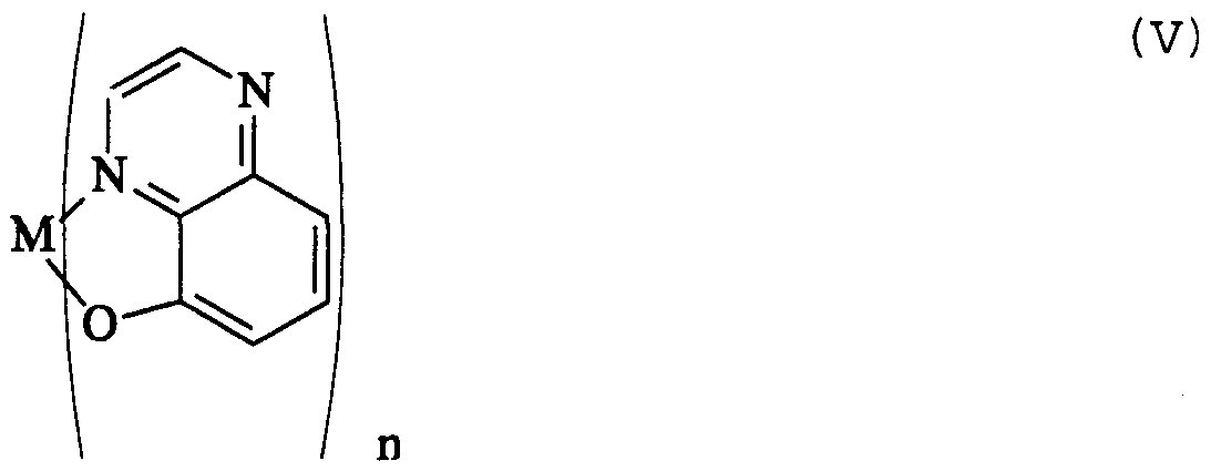


Claims


Priority Applications (4)
| Application Number | Priority Date | Filing Date | Title |
|---|---|---|---|
| AU57210/98A AU5721098A (en) | 1996-12-23 | 1997-12-23 | An organic light emitting device containing a protection layer |
| CA002275542A CA2275542A1 (en) | 1996-12-23 | 1997-12-23 | An organic light emitting device containing a protection layer |
| EP97953470A EP0950254A4 (en) | 1996-12-23 | 1997-12-23 | An organic light emitting device containing a protection layer |
| JP52908098A JP2001527688A (en) | 1996-12-23 | 1997-12-23 | Organic light emitting device containing protective layer |
Applications Claiming Priority (22)
| Application Number | Priority Date | Filing Date | Title |
|---|---|---|---|
| US77181596A | 1996-12-23 | 1996-12-23 | |
| US08/772,332 US5834893A (en) | 1996-12-23 | 1996-12-23 | High efficiency organic light emitting devices with light directing structures |
| US08/774,119 US6046543A (en) | 1996-12-23 | 1996-12-23 | High reliability, high efficiency, integratable organic light emitting devices and methods of producing same |
| US08/774,120 US5811833A (en) | 1996-12-23 | 1996-12-23 | Electron transporting and light emitting layers based on organic free radicals |
| US81497697A | 1997-03-11 | 1997-03-11 | |
| US08/821,380 US5986401A (en) | 1997-03-20 | 1997-03-20 | High contrast transparent organic light emitting device display |
| US08/838,099 US5861219A (en) | 1997-04-15 | 1997-04-15 | Organic light emitting devices containing a metal complex of 5-hydroxy-quinoxaline as a host material |
| US08/850,264 US6045930A (en) | 1996-12-23 | 1997-05-02 | Materials for multicolor light emitting diodes |
| US08/865,491 US5998803A (en) | 1997-05-29 | 1997-05-29 | Organic light emitting device containing a hole injection enhancement layer |
| US08/925,403 US5874803A (en) | 1997-09-09 | 1997-09-09 | Light emitting device with stack of OLEDS and phosphor downconverter |
| US08/928,800 | 1997-09-12 | ||
| US08/838,099 | 1997-09-12 | ||
| US08/774,120 | 1997-09-12 | ||
| US08/865,491 | 1997-09-12 | ||
| US08/821,380 | 1997-09-12 | ||
| US08/814,976 | 1997-09-12 | ||
| US08/928,800 US5981306A (en) | 1997-09-12 | 1997-09-12 | Method for depositing indium tin oxide layers in organic light emitting devices |
| US08/772,332 | 1997-09-12 | ||
| US08/925,403 | 1997-09-12 | ||
| US08/850,264 | 1997-09-12 | ||
| US08/774,119 | 1997-09-12 | ||
| US08/771,815 | 1997-09-12 |
Publications (2)
| Publication Number | Publication Date |
|---|---|
| WO1998028767A1 true WO1998028767A1 (en) | 1998-07-02 |
| WO1998028767A9 WO1998028767A9 (en) | 1998-11-05 |
Family
ID=27582810
Family Applications (1)
| Application Number | Title | Priority Date | Filing Date |
|---|---|---|---|
| PCT/US1997/023952 WO1998028767A1 (en) | 1996-12-23 | 1997-12-23 | An organic light emitting device containing a protection layer |
Country Status (5)
| Country | Link |
|---|---|
| EP (1) | EP0950254A4 (en) |
| JP (1) | JP2001527688A (en) |
| CN (1) | CN1245581A (en) |
| CA (1) | CA2275542A1 (en) |
| WO (1) | WO1998028767A1 (en) |
Cited By (22)
| Publication number | Priority date | Publication date | Assignee | Title |
|---|---|---|---|---|
| WO2000004594A1 (en) * | 1998-07-20 | 2000-01-27 | Motorola, Inc. | Organic electroluminescent apparatus |
| JP2000068060A (en) * | 1998-08-13 | 2000-03-03 | Tdk Corp | Organic el element and its manufacture |
| EP1026757A2 (en) * | 1998-11-05 | 2000-08-09 | Eastman Kodak Company | Organic electroluminescent device with a non-conductive fluorocarbon polymer layer |
| DE10035606A1 (en) * | 1999-07-21 | 2001-05-23 | Nec Corp | Organic electroluminescent plate and filter therefor |
| WO2002021557A1 (en) * | 2000-09-06 | 2002-03-14 | Osram Opto Semiconductors Gmbh | Encapsulation for oled devices |
| US6682782B2 (en) * | 2000-07-03 | 2004-01-27 | Korea Research Institute Of Chemical Technology | Organic compound having an acetylene group, vacuum deposition polymerization thereof, deposited polymerized thin film, and electroluminescence device containing same |
| WO2004031247A1 (en) * | 2002-09-30 | 2004-04-15 | Infineon Technologies Ag | Pentaarylcyclopentadienyl units as active units in resistive memory elements |
| US6873093B2 (en) | 2003-02-28 | 2005-03-29 | Motorola, Inc. | Organic light emitting diode display structure |
| US7166007B2 (en) | 1999-12-17 | 2007-01-23 | Osram Opto Semiconductors Gmbh | Encapsulation of electronic devices |
| US7417247B2 (en) | 2002-09-30 | 2008-08-26 | Infineon Technologies, Ag | Pentaarylcyclopentadienyl units as active units in resistive memory elements |
| US7915815B2 (en) | 2005-03-11 | 2011-03-29 | Novaled Ag | Transparent light-emitting component |
| US7943963B2 (en) | 2004-03-24 | 2011-05-17 | Hitachi Displays, Ltd. | Organic light-emitting display device |
| US8344360B2 (en) | 1999-12-17 | 2013-01-01 | Osram Opto Semiconductor Gmbh | Organic electronic devices with an encapsulation |
| US8637854B2 (en) | 2008-05-16 | 2014-01-28 | Lg Chem, Ltd. | Stacked organic light emitting diode |
| US8951645B2 (en) | 2004-04-09 | 2015-02-10 | Lg Chem, Ltd. | Stacked organic light emitting device having high efficiency and high brightness |
| US9023492B2 (en) | 2008-11-13 | 2015-05-05 | Lg Chem, Ltd. | Low voltage-driven organic electroluminescence device, and manufacturing method thereof |
| US9028974B2 (en) | 2006-03-07 | 2015-05-12 | Lg Chem, Ltd. | OLED and fabricating method of the same |
| US9048439B2 (en) | 2010-03-31 | 2015-06-02 | Semiconductor Energy Laboratory Co., Ltd. | Light-emitting element, light-emitting device, electronic device, and lighting device comprising a metal complex having a metal-oxygen bond and an aromatic ligand |
| US9520573B2 (en) | 2011-05-16 | 2016-12-13 | Qd Vision, Inc. | Device including quantum dots and method for making same |
| US9525148B2 (en) | 2008-04-03 | 2016-12-20 | Qd Vision, Inc. | Device including quantum dots |
| US9793505B2 (en) | 2008-04-03 | 2017-10-17 | Qd Vision, Inc. | Light-emitting device including quantum dots |
| WO2018223647A1 (en) | 2017-06-05 | 2018-12-13 | Boe Technology Group Co., Ltd. | Light-emitting diode, array substrate, and method of making the same |
Families Citing this family (24)
| Publication number | Priority date | Publication date | Assignee | Title |
|---|---|---|---|---|
| JP3907142B2 (en) * | 1998-08-18 | 2007-04-18 | 富士フイルム株式会社 | Organic electroluminescent device material and organic electroluminescent device using the same |
| GB9907931D0 (en) * | 1999-04-07 | 1999-06-02 | Univ Edinburgh | An optoelectronic display |
| JP4420486B2 (en) * | 1999-04-30 | 2010-02-24 | 出光興産株式会社 | Organic electroluminescence device and method for producing the same |
| DE10207859A1 (en) * | 2002-02-20 | 2003-09-04 | Univ Dresden Tech | Doped organic semiconductor material and process for its production |
| JP4222339B2 (en) * | 2002-10-03 | 2009-02-12 | セイコーエプソン株式会社 | Display panel and electronic device including the display panel |
| JP4365196B2 (en) * | 2002-12-27 | 2009-11-18 | 富士フイルム株式会社 | Organic electroluminescence device |
| JP4736352B2 (en) * | 2003-06-16 | 2011-07-27 | 三菱化学株式会社 | Field effect transistor |
| JP4396163B2 (en) * | 2003-07-08 | 2010-01-13 | 株式会社デンソー | Organic EL device |
| US6861664B2 (en) * | 2003-07-25 | 2005-03-01 | Xerox Corporation | Device with n-type semiconductor |
| KR20060113884A (en) * | 2003-08-05 | 2006-11-03 | 테크니체 우니베르시테트 브라운츠바이그 차롤오-빌헬미나 | Use of a layer consisting of hydrophobic, linear or two-dimensional polycyclic aromatics as a barrier layer or an encapsulation and electric components constructed with a layer of this type and comprising organic polymers |
| DE10338406A1 (en) * | 2003-08-18 | 2005-03-24 | Novaled Gmbh | Doped organic semiconductor materials and process for their preparation |
| JP2008510312A (en) * | 2004-08-19 | 2008-04-03 | エルジー・ケム・リミテッド | Organic light emitting device including buffer layer and method of manufacturing the same |
| DE502005009415D1 (en) * | 2005-05-27 | 2010-05-27 | Novaled Ag | Transparent organic light emitting diode |
| KR101254589B1 (en) | 2006-06-29 | 2013-04-15 | 엘지디스플레이 주식회사 | The organic electro-luminescence device and method for fabricating of the same |
| CN100521286C (en) * | 2006-10-18 | 2009-07-29 | 中国科学院半导体研究所 | Organic light emitting diode adopting polarized cavity injection structure |
| JP2008235193A (en) * | 2007-03-23 | 2008-10-02 | Fujifilm Corp | Organic electroluminescent device |
| US9123667B2 (en) * | 2011-10-04 | 2015-09-01 | Universal Display Corporation | Power-efficient RGBW OLED display |
| JP6130629B2 (en) * | 2012-06-21 | 2017-05-17 | ユー・ディー・シー アイルランド リミテッド | Organic electroluminescence device |
| DE102012217587A1 (en) * | 2012-09-27 | 2014-03-27 | Siemens Aktiengesellschaft | Salts of cyclopentadiene as n-dopants for organic electronics |
| WO2015081327A1 (en) * | 2013-11-27 | 2015-06-04 | Chou Stephen Y | Light emitting diode, photodiode, displays, and method for forming the same |
| CN105226184B (en) * | 2014-06-26 | 2020-01-14 | 潘才法 | Electroluminescent device comprising stable organic radical compound |
| CN105244447B (en) * | 2015-09-01 | 2018-09-14 | 华南理工大学 | A kind of planar heterojunction Organic Light Emitting Diode and preparation method thereof |
| KR102475330B1 (en) * | 2016-12-01 | 2022-12-08 | 도레이 카부시키가이샤 | organic EL display |
| CN112599704B (en) * | 2020-12-14 | 2022-07-12 | 武汉华星光电半导体显示技术有限公司 | Display panel and manufacturing method thereof |
Citations (1)
| Publication number | Priority date | Publication date | Assignee | Title |
|---|---|---|---|---|
| US4950950A (en) * | 1989-05-18 | 1990-08-21 | Eastman Kodak Company | Electroluminescent device with silazane-containing luminescent zone |
Family Cites Families (6)
| Publication number | Priority date | Publication date | Assignee | Title |
|---|---|---|---|---|
| US5118986A (en) * | 1989-06-30 | 1992-06-02 | Ricoh Company, Ltd. | Electroluminescent device |
| GB9215928D0 (en) * | 1992-07-27 | 1992-09-09 | Cambridge Display Tech Ltd | Manufacture of electroluminescent devices |
| JPH06203963A (en) * | 1993-01-08 | 1994-07-22 | Idemitsu Kosan Co Ltd | Organic electroluminescent element |
| JPH06325872A (en) * | 1993-05-18 | 1994-11-25 | Mitsubishi Kasei Corp | Organic electroluminescent element |
| JPH08288068A (en) * | 1995-04-14 | 1996-11-01 | Toyota Central Res & Dev Lab Inc | Organic electroluminescent element |
| EP0946993B8 (en) * | 1996-09-04 | 2007-09-12 | Cambridge Display Technology Limited | Electrode deposition for organic light-emitting devices |
-
1997
- 1997-12-23 EP EP97953470A patent/EP0950254A4/en not_active Withdrawn
- 1997-12-23 CA CA002275542A patent/CA2275542A1/en not_active Abandoned
- 1997-12-23 WO PCT/US1997/023952 patent/WO1998028767A1/en not_active Application Discontinuation
- 1997-12-23 CN CN97181500A patent/CN1245581A/en active Pending
- 1997-12-23 JP JP52908098A patent/JP2001527688A/en active Pending
Patent Citations (1)
| Publication number | Priority date | Publication date | Assignee | Title |
|---|---|---|---|---|
| US4950950A (en) * | 1989-05-18 | 1990-08-21 | Eastman Kodak Company | Electroluminescent device with silazane-containing luminescent zone |
Cited By (36)
| Publication number | Priority date | Publication date | Assignee | Title |
|---|---|---|---|---|
| WO2000004594A1 (en) * | 1998-07-20 | 2000-01-27 | Motorola, Inc. | Organic electroluminescent apparatus |
| JP2000068060A (en) * | 1998-08-13 | 2000-03-03 | Tdk Corp | Organic el element and its manufacture |
| EP1026757A3 (en) * | 1998-11-05 | 2003-09-03 | Eastman Kodak Company | Organic electroluminescent device with a non-conductive fluorocarbon polymer layer |
| EP1026757A2 (en) * | 1998-11-05 | 2000-08-09 | Eastman Kodak Company | Organic electroluminescent device with a non-conductive fluorocarbon polymer layer |
| US6706425B2 (en) | 1999-07-21 | 2004-03-16 | Nec Corporation | Organic EL panel and filter for same |
| DE10035606A1 (en) * | 1999-07-21 | 2001-05-23 | Nec Corp | Organic electroluminescent plate and filter therefor |
| DE10035606C2 (en) * | 1999-07-21 | 2002-03-14 | Nec Corp | Organic electroluminescent display element and filter therefor |
| US7166007B2 (en) | 1999-12-17 | 2007-01-23 | Osram Opto Semiconductors Gmbh | Encapsulation of electronic devices |
| US7394153B2 (en) | 1999-12-17 | 2008-07-01 | Osram Opto Semiconductors Gmbh | Encapsulation of electronic devices |
| US7419842B2 (en) | 1999-12-17 | 2008-09-02 | Osram Gmbh | Encapsulation of electroluminescent devices with shaped spacers |
| US7432533B2 (en) | 1999-12-17 | 2008-10-07 | Osram Gmbh | Encapsulation of electronic devices with shaped spacers |
| US8344360B2 (en) | 1999-12-17 | 2013-01-01 | Osram Opto Semiconductor Gmbh | Organic electronic devices with an encapsulation |
| US6682782B2 (en) * | 2000-07-03 | 2004-01-27 | Korea Research Institute Of Chemical Technology | Organic compound having an acetylene group, vacuum deposition polymerization thereof, deposited polymerized thin film, and electroluminescence device containing same |
| WO2002021557A1 (en) * | 2000-09-06 | 2002-03-14 | Osram Opto Semiconductors Gmbh | Encapsulation for oled devices |
| US7255823B1 (en) | 2000-09-06 | 2007-08-14 | Institute Of Materials Research And Engineering | Encapsulation for oled devices |
| WO2004031247A1 (en) * | 2002-09-30 | 2004-04-15 | Infineon Technologies Ag | Pentaarylcyclopentadienyl units as active units in resistive memory elements |
| US7417247B2 (en) | 2002-09-30 | 2008-08-26 | Infineon Technologies, Ag | Pentaarylcyclopentadienyl units as active units in resistive memory elements |
| US6873093B2 (en) | 2003-02-28 | 2005-03-29 | Motorola, Inc. | Organic light emitting diode display structure |
| US7943963B2 (en) | 2004-03-24 | 2011-05-17 | Hitachi Displays, Ltd. | Organic light-emitting display device |
| US9647225B2 (en) | 2004-04-09 | 2017-05-09 | Lg Chem, Ltd. | Stacked organic light emitting device having high efficiency and high brightness |
| US8951645B2 (en) | 2004-04-09 | 2015-02-10 | Lg Chem, Ltd. | Stacked organic light emitting device having high efficiency and high brightness |
| US7915815B2 (en) | 2005-03-11 | 2011-03-29 | Novaled Ag | Transparent light-emitting component |
| US9028974B2 (en) | 2006-03-07 | 2015-05-12 | Lg Chem, Ltd. | OLED and fabricating method of the same |
| US9793505B2 (en) | 2008-04-03 | 2017-10-17 | Qd Vision, Inc. | Light-emitting device including quantum dots |
| US9525148B2 (en) | 2008-04-03 | 2016-12-20 | Qd Vision, Inc. | Device including quantum dots |
| US9755172B2 (en) | 2008-04-03 | 2017-09-05 | Qd Vision, Inc. | Device including quantum dots |
| US10164205B2 (en) | 2008-04-03 | 2018-12-25 | Samsung Research America, Inc. | Device including quantum dots |
| US10333090B2 (en) | 2008-04-03 | 2019-06-25 | Samsung Research America, Inc. | Light-emitting device including quantum dots |
| US11005058B2 (en) | 2008-04-03 | 2021-05-11 | Samsung Research America, Inc. | Light-emitting device including quantum dots |
| US8637854B2 (en) | 2008-05-16 | 2014-01-28 | Lg Chem, Ltd. | Stacked organic light emitting diode |
| US9023492B2 (en) | 2008-11-13 | 2015-05-05 | Lg Chem, Ltd. | Low voltage-driven organic electroluminescence device, and manufacturing method thereof |
| US9048439B2 (en) | 2010-03-31 | 2015-06-02 | Semiconductor Energy Laboratory Co., Ltd. | Light-emitting element, light-emitting device, electronic device, and lighting device comprising a metal complex having a metal-oxygen bond and an aromatic ligand |
| US9520573B2 (en) | 2011-05-16 | 2016-12-13 | Qd Vision, Inc. | Device including quantum dots and method for making same |
| WO2018223647A1 (en) | 2017-06-05 | 2018-12-13 | Boe Technology Group Co., Ltd. | Light-emitting diode, array substrate, and method of making the same |
| EP3635787A4 (en) * | 2017-06-05 | 2021-01-06 | BOE Technology Group Co., Ltd. | Light-emitting diode, array substrate, and method of making the same |
| US11114638B2 (en) | 2017-06-05 | 2021-09-07 | Hefei Xinsheng Optoelectronics Technology Co., Ltd. | Light-emitting diode, array substrate, and method of making the same |
Also Published As
| Publication number | Publication date |
|---|---|
| CA2275542A1 (en) | 1998-07-02 |
| CN1245581A (en) | 2000-02-23 |
| EP0950254A1 (en) | 1999-10-20 |
| EP0950254A4 (en) | 2002-11-27 |
| JP2001527688A (en) | 2001-12-25 |
Similar Documents
| Publication | Publication Date | Title |
|---|---|---|
| WO1998028767A1 (en) | An organic light emitting device containing a protection layer | |
| WO1998028767A9 (en) | An organic light emitting device containing a protection layer | |
| US7488542B2 (en) | OLEDs doped with phosphorescent compounds | |
| US5861219A (en) | Organic light emitting devices containing a metal complex of 5-hydroxy-quinoxaline as a host material | |
| JP4511024B2 (en) | Highly transparent non-metallic cathode | |
| US6045930A (en) | Materials for multicolor light emitting diodes | |
| US6030715A (en) | Azlactone-related dopants in the emissive layer of an OLED | |
| US5998803A (en) | Organic light emitting device containing a hole injection enhancement layer | |
| US6413656B1 (en) | Reduced symmetry porphyrin molecules for producing enhanced luminosity from phosphorescent organic light emitting devices | |
| US5811833A (en) | Electron transporting and light emitting layers based on organic free radicals | |
| US6451455B1 (en) | Metal complexes bearing both electron transporting and hole transporting moieties | |
| KR20000062301A (en) | An organic light emitting device containing a protection layer | |
| TW385620B (en) | An organic light emitting device containing a protection layer |
Legal Events
| Date | Code | Title | Description |
|---|---|---|---|
| WWE | Wipo information: entry into national phase |
Ref document number: 97181500.3 Country of ref document: CN |
|
| AK | Designated states |
Kind code of ref document: A1 Designated state(s): AL AM AT AU AZ BA BB BG BR BY CA CH CN CU CZ DE DK EE ES FI GB GE GH GW HU ID IL IS JP KE KG KP KR KZ LC LK LR LS LT LU LV MD MG MK MN MW MX NO NZ PL PT RO RU SD SE SG SI SK SL TJ TM TR TT UA UG UZ VN YU ZW AM AZ BY KG KZ MD RU TJ TM |
|
| AL | Designated countries for regional patents |
Kind code of ref document: A1 Designated state(s): GH GM KE LS MW SD SZ UG ZW AT BE CH DE DK ES FI FR GB GR IE IT LU |
|
| DFPE | Request for preliminary examination filed prior to expiration of 19th month from priority date (pct application filed before 20040101) | ||
| COP | Corrected version of pamphlet |
Free format text: PAGES 1/27-27/27, DRAWINGS, REPLACED BY NEW PAGES 1/22-22/22; DUE TO LATE TRANSMITTAL BY THE RECEIVING OFFICE |
|
| 121 | Ep: the epo has been informed by wipo that ep was designated in this application | ||
| WWE | Wipo information: entry into national phase |
Ref document number: 1997953470 Country of ref document: EP |
|
| ENP | Entry into the national phase |
Ref document number: 2275542 Country of ref document: CA Ref document number: 2275542 Country of ref document: CA Kind code of ref document: A |
|
| WWE | Wipo information: entry into national phase |
Ref document number: 1019997005719 Country of ref document: KR |
|
| ENP | Entry into the national phase |
Ref document number: 1998 529080 Country of ref document: JP Kind code of ref document: A |
|
| WWP | Wipo information: published in national office |
Ref document number: 1997953470 Country of ref document: EP |
|
| REG | Reference to national code |
Ref country code: DE Ref legal event code: 8642 |
|
| WWP | Wipo information: published in national office |
Ref document number: 1019997005719 Country of ref document: KR |
|
| WWW | Wipo information: withdrawn in national office |
Ref document number: 1019997005719 Country of ref document: KR |
|
| WWW | Wipo information: withdrawn in national office |
Ref document number: 1997953470 Country of ref document: EP |