WO1994010641A1 - Audio/video computer architecture - Google Patents
Audio/video computer architecture Download PDFInfo
- Publication number
- WO1994010641A1 WO1994010641A1 PCT/US1992/009349 US9209349W WO9410641A1 WO 1994010641 A1 WO1994010641 A1 WO 1994010641A1 US 9209349 W US9209349 W US 9209349W WO 9410641 A1 WO9410641 A1 WO 9410641A1
- Authority
- WO
- WIPO (PCT)
- Prior art keywords
- address
- bus
- cpu
- audio
- dma
- Prior art date
Links
Classifications
-
- G—PHYSICS
- G06—COMPUTING; CALCULATING OR COUNTING
- G06T—IMAGE DATA PROCESSING OR GENERATION, IN GENERAL
- G06T1/00—General purpose image data processing
- G06T1/20—Processor architectures; Processor configuration, e.g. pipelining
Definitions
- PCT Patent Application Serial No. entitled METHOD FOR CONTROLLING A SPRYTE RENDERING PROCESSOR, by inventors Robert J. Mical, et al., filed concurrently herewith, Attorney Docket No. MDIO3040, and also to U.S. Patent Application Serial No. , bearing the same title, same inventors and also filed concurrently herewith;
- PCT Patent Application Serial No entitled SPRYTE RENDERING SYSTEM WITH IMPROVED CORNER CALCULATING ENGINE AND IMPROVED POLYGON-PAINT ENGINE, by inventors David L. Needle, et al., filed concurrently herewith, Attorney Docket No. MDI04232, and also to U.S.
- the invention involves an interactive high-performance video and audio entertainment and education system, and more particularly, to techniques for reducing the cost and improving the performance and realism of such a system.
- Interactive multi-media systems are systems in which the flow of an audio/visual presentation is adjusted in response to signals provided interactively by a user.
- Such systems typically run game programs or education programs, which are purchased by the consumer and loaded into the system.
- Consumer interactive multi-media systems are or have been available from such companies as Nintendo K.K., Sega Enterprises, Atari Corp., and Commodore-Amiga, among others.
- manufacturers of consumer interactive multi-media systems have had to make significant compromises in the realism of sounds and video images created by the system, in order to maintain a low price for the consumer market.
- ordinary television sets have typically been used as the video output device of consumer interactive multi-media systems.
- a television display can support a maximum resolution of approximately 480 pixels vertically and 640 pixels horizontally.
- full color resolution is typically considered to require 8 bits of data for each of three primary colors (such as red, green, blue) for each of the pixels. Accordingly, if such systems were to represent a video frame in memory with full color and pixel resolution, a total of 24 bits x 480 x 640 pixels, or nearly one megabyte of memory, would be required. Techniques have been developed to reduce the number of bits required to represent a particular pixel color with varying degrees of flexibility, but a very large amount of memory was still required to store the frame.
- the realism of a multi-media experience is also affected by the frequency with which an animated video image can be updated.
- the system should be able to update all 480 x 640 pixels once each frame time (30 times per second, for NTSC television).
- Such a pixel rendering rate of over nine million pixels per second is far beyond the capabilities of conventional low cost multi-media systems, especially if any significant calculations need to be performed.
- Various techniques have been devised to reduce the required pixel writing bandwidth, but again, only at the expense of realism. For example, many systems form a "background" image, covering the entire frame, and a separate "sprite" image, covering only a small rectangular region in the frame.
- the pixel writing bandwidth is greatly reduced by altering the contents and position of only the sprite image at the rate of 30 times per second. But an unchanging background image reduces the realism of the visual experience.
- Various system architectures have been used in multi-media systems.
- a CPU renders and modifies images in a video memory which is continuously being read out and displayed via a separate port.
- Such an arrangement keeps the cost of the system low since the number of separate components is small.
- all rendering and animation in such a system is limited to the speed of the CPU and memory.
- a high-speed CPU and a graphics accelerator are both coupled to a memory in master/slave relationship.
- the CPU may be able to manipulate graphic images in the memory, but most of the manipulation is performed by the graphics accelerator in response to commands issued from the CPU to the graphics accelerator.
- the frame buffer data is continuously read out via a separate port of the memory and provided to the display.
- Systems such as these typically operate at full 24-bit color designations, with a full 640 by 480 pixel resolution. In order to update the entire frame buffer at the NTSC 30Hz rate, such systems require powerful hardware which is extremely expensive and does not reduce the memory requirements mentioned above. These architectures are not often used in consumer systems.
- a consumer interactive multi-media system in which a CPU is loosely coupled with system memory, and a graphics manipulation processor (“spryte engine”) performs substantially all of the graphics rendering and manipulation functions.
- the spryte system accesses the memory by DMA and has a significantly higher bus priority than does the CPU.
- graphic images may be stored, rendered and manipulated in a compressed format, both in terms of the number of bits stored per pixel and in terms of the number of pixels stored per frame.
- the frame buffer information is read out from a separate serial port of the system memory and expanded to full 640 by 480 pixel format, with a substantially full 24-bit color resolution, all as part of the video display path.
- the resulting images are nearly of broadcast quality and can be made highly realistic.
- Commands to modify CLUT tables or other parameters in the video display path are provided via the display path itself, and therefore are automatically synchronized appropriately with pixels, scan lines, fields and frames.
- the system also includes an audio manipulation processor which receives audio sample data via DMA from the system memory, also with a higher bus priority than the CPU.
- Fig. 1 is a block diagram of major components of the system
- Fig. 2 is a symbolic block diagram of the address manipulator of Fig. 1;
- Fig. 3 is a block diagram of part of the address generator of Fig. 2;
- Fig. 4 is a block diagram of the stack address logic of Fig. 3;
- Fig. 5 is a symbolic block diagram of part of the player bus interface of Fig. 2;
- Fig. 6 is a symbolic bock diagram of the audio/video processor of Fig. 1; and Fig. 7 is a block diagram of the left address pad logic of Fig. 3.
- FIG. 1 is a block diagram showing major components of a consumer interactive multi-media system according to the invention. It comprises a CPU 102, which may be an ARM 60 RISC processor manufactured by Advanced RISC Machines, Ltd., Swaffham Bulbeck, Cambridge, U.K.
- the ARM 60 is described in Advanced RISC Machines, "ARM 60 Datasheet” (1992), incorporated herein by reference.
- the ARM 60 is a relatively low-cost, general-purpose 32- bit single-chip microprocessor.
- the address pins of CPU 102 are coupled to a 32-bit address bus 104, which is provided as an input to an address manipulator chip 106.
- the address manipulator chip 106 contains, among other things, an address generator for providing DMA- generated addresses to system memory, as well as addresses from other sources; a D-bus arbiter; two spryte engines; and interfaces to a player bus, a slow bus and a set of external processors.
- the address manipulator chip 106 generates addresses for system memory 108, which includes a left memory bank 108A and a right memory bank 108B.
- System memory is 32-bits wide, the high-order 16 bits of each 32-bit word being in left memory 108A and the low-order 16 bits being in right memory 108B.
- the CPU 102 addresses system memory in words or bytes, but the address manipulator chip 106 can address each half of the memory entirely independently.
- Address manipulator chip 106 provides addresses and control signals to left memory 108A over an LA bus 110 and an LCTL bus 112, respectively, and provides addresses and control signals to right memory
- System memory 108 can include one or two "sets" of video RAM (VRAM) and zero, one or two sets of DRAM.
- VRAM video RAM
- a set of VRAM contains 512 k bytes of left memory and 512 k bytes of right memory, for a total of one megabyte.
- a set of DRAM is, depending on the system configuration, one, four or 16 megabytes long. Other options may also be made available. As with VRAM, half of each set is located in the left bank of memory and the other half is located in the right bank of memory.
- System memory 108 is considered big-endian.
- VRAM any standard DRAM will suffice.
- VRAM an array made up of those described in NEC Electronics, Inc., " ⁇ PD 482234, 482235 Video RAM”, Advance Copy Datasheet (2/92), or in NEC Corporation, “ ⁇ PD 482445 256K-word x 16-bit Dual Port Graphics Buffer”, Preliminary Datasheet (Jan. 1992), both of which are incorporated herein by reference, are preferred.
- the former reference describes a two megabit VRAM and the later describes a four megabit VRAM.
- All of the left and right bank system memory sets receive the respective left and right half addresses generated by the address manipulator chip 106.
- All of the left bank sets also include a data port which are coupled bi-directionally with a left half data bus D(31:16) 118.
- the data ports of all of the sets of right bank memory are coupled bi-directionally with a right half data bus D(15:0) 120.
- the VRAM sets also have a serial port S, which is coupled bi-directionally with an S(31:0) bus 122.
- a useful characteristic of many address-multiplexed DRAM and VRAM devices is "page mode" operation.
- the multiplexed nature of the address port of these memories requires that first a row (page) address be strobed into the device, then the column address be strobed in.
- the row address is received by the device, it accesses an entire row (page) of memory and makes it available to the column selector.
- the column address is provided to the column selector.
- the quantity of addresses in a page is determined by the number of bits of address value provided with a row address strobe (RAS), and the number of bits which are selected by a column address is the data width of the device. For example, one of the NEC VRAM devices mentioned above is organized as 256k by 8 bits.
- Each row address selects one of 512 rows of 512 addresses each, and each column address selects one of the 512 8-bit bytes contained in the selected row.
- the act of using multiple column address strobes for a single row address strobe is called "page mode operation" , and advantageously avoids the time penalty of having to re-establish the row address for each access.
- VRAM devices there is also a static holding register that can be loaded with a page of data from the internal DRAM. The contents of this holding register can be clocked out a serial data port of the device.
- 512 8-bit bytes of data are loaded into the static holding register in response to an S-port read transfer command issued to the device.
- serial clock (SC)
- the NEC device also permits the serial port to be used to write a page of data into a selected row of VRAM.
- the NEC device described above splits the static holding register into two halves (not to be confused with the two halves (banks) of system memory), and the device will respond to a command to load one half row while the other half-row is shifting out. In this manner, a continuous stream of data may be shifted out of the S-port of the VRAM without having to pause for an S-port read transfer cycle.
- the VRAM generates a QSF signal indicating which half page is currently being clocked out.
- the QSF signal is coupled over lines 124 and 126 (for the left and right system memory banks, respectively) , to respective LQSF and RQSF inputs of the address manipulator 106.
- address manipulator chip 106 also provides and receives control signals to and from the CPU 102 over lines 128, and is also coupled bi- directionally with the left and right data buses 118 and 120.
- Address manipulator chip 106 also interfaces to a slow bus 130, which is an 8-bit bus for accessing such devices as a CPU ROM 132, a battery-backed SRAM 133, and/or various front panel devices 134. It may also support additional CPU-accessible RAM, and may also support an FM sound generator device.
- the slow bus 130 includes 14 bits of the address bus 104 A(16:2), an 8- bit data bus PD(7:0), a PDRDB read strobe, a PDWRB write strobe, and various control lines. PDRDB and PDWRB are used to carry the two low-order address lines for accessing the 8-bit wide CPU ROM 132.
- Address manipulator chip 106 also interfaces to a player bus 136, which is used to connect the system to various user input/output devices such as joysticks, 3- D glasses, hand controllers and steering wheels, and also to auxiliary devices such IR pods for wireless operation and game saver cartridges.
- the player bus 136 is a serial bus.
- the player bus is described in the above -mentioned PLAYER BUS APPARATUS AND METHOD application. Briefly, it includes a clock line PBCK which is driven by the address manipulator chip 106, a data output line PDBO which is also driven by address manipulator chip 106, and a data input line PBDI which is driven by an external device.
- I/O controllers on the player bus 136 are daisy chained with the two serial data lines feeding through each of the controllers.
- the protocol automatically identifies each controller device type, with multiple identical controllers identified individually. No user settings are required.
- Left and right audio signals are also transmitted over lines PBLA and PBRA on the player bus 136 to external devices.
- Address manipulator chip 106 is also coupled to a control bus 138, which is used to send and receive control signals to and from other processors in the system of Fig. 1.
- the system of Fig. 1 further includes an audio/video processor chip 140 which is coupled bi-directionally to both halves 118 and 120 of the D-bus, and coupled to receive data from the 32-bit wide S bus 122. Audio/video processor chip 140 is also coupled to the control bus 138, and is coupled to receive address bits A(15:2) from the system address bus 104.
- the audio/video processor chip 140 generally includes display path circuitry, an audio subsystem, timers, an interrupt controller, an expansion bus interface and a watchdog timer.
- the expansion bus interface couples to an expansion bus 142 which includes control lines 144 and an 8-bit bus 146 carrying multiplexed address and data information.
- the expansion bus 142 supports such devices as CD/CD-ROM player 148 and optional expansion bus RAM 150.
- the CD/CD-ROM player 148 is built into the housing of the system of Fig. 1 and provides the primary mechanism by which software is loaded into the system for execution on the CPU 102. It may also be used to play standard CD/audio disks, as well as view standard photo-CD disks and handle other non-software formats.
- the audio/video processor 140 communicates with audio/video output circuitry 152 via audio lines 157, control lines 156, and a 12- or 24-bit AD bus 158.
- the audio lines 157 and the AD bus 158 are uni-directional from the audio/video processor 140 to the audio/video encoder 152.
- the audio/video output circuitry 152 generally generates the video timing and output video waveforms. It provides a composite video output, an RF output for connection to a standard television, an SVHS output, and separate left and right audio signal outputs. As previously mentioned, the audio outputs are included in the player bus 136.
- the AD lines 158 carry pixel data in RGB format at the rate of 24 bits per pixel time.
- One pixel time is approximately 80nS, the time required for the display scan to traverse one square pixel space in the NTSC standard.
- the AD lines 158 can be multiplexed to actually provide half of a pixel color every 40nS (25MHz) using only 12 of the 24 AD signal lines.
- the audio output data on lines 157 is provided as a serial stream of digital data, at the standard CD-audio rate of one 16-bit left and right sample every 22.7 microseconds (44.1kHz) .
- the system of Fig. 1 also includes a video input device 160 for "slipstream" capture of externally supplied video signals.
- the video input device 160 is coupled to the control bus 138 and provides a 32-bit output to the S-bus 122.
- the video input device 160 also provides synchronization signals to the audio/video output circuitry 152.
- the video input device 160 When externally supplied video signals are to be captured, or in some way coordinated with the remainder of the system of Fig. 1, the video input device 160 derives a video clock of approximately 25MHz (twice the square pixel frequency) from the analog video input signal. The system of Fig. 1 then uses this clock signal, rather than a local crystal oscillator, to drive the entire video display path from system memory, through the audio/video processor 140, and through the audio/video output circuitry 152. This procedure is referred to as "GenLock" . When the system is GenLocked, the video input device 160 decodes the video signal from the external analog input, digitizes it into 24-bit words each representing a respective pixel. This pixel data is processed down to a 16-bit format useful for the system of Fig.
- the system transmits a line of incoming pixel data in a burst over the S-bus 122, into VRAM.
- the S-bus is 32 bits wide, so two 16-bit pixels are transferred at a time.
- captured video data may be transmitted over the S-bus 122 directly into the audio/video processor 140 for writing out to the audio/video output circuitry 152, either in the 16-bit or 24-bit format.
- video input device 160 can also be used to capture software and other forms of data which are being downloaded over the external video input path.
- the external video input may be connected to a cable TV network cable.
- the cable TV head end equipment may download a game program over an otherwise unused cable channel.
- Video input device 160 would capture the software and burst it into system memory 108 in the same manner as captured video pixels are transmitted to system memory 108, except that this data can be transferred in an uncompressed 32-bit wide format. Instead of displaying the data, the system of Fig. 1 would execute it on the CPU 102.
- downloaded software may be received by a device on the expansion bus 142 and accessed by the system of Fig. 1 in a manner which is similar to the accessing of CD/CD-ROM player 148.
- the system of Fig. 1 also includes an audio input device 162 to capture externally supplied audio data, to compliment the externally supplied video data.
- the 4-wire output of audio/video input device 162 is coupled over lines 164 to the audio subsystem in the audio/video processor 140.
- the audio/video processor is programmable by the CPU 102 to accept the data in any of several predefined serial formats. Audio input device 162 is also coupled to the control bus 138.
- the system of Fig. 1 also includes a decompression co-processor 166 which is coupled to the control bus 138, to bits A(15:2) of the system address bus 104, and to both halves 118 and 120 of the D bus.
- Decompression co-processor 166 is used to decompress software or image data in system memory 108. Typically, such data was previously loaded into the system from the CD/CD-ROM player 148 or from another external source.
- the system of Fig. 1 does not require a user to perform any system configuration process, although it does permit a user to set certain preferences to optimize the audio/video experience in a particular environment.
- a section of system memory starting at address zero and extending to either 0, 8, 16 or 32 K bytes, may be defined as SYSRAM. If SYSRAM is available in a given embodiment, the size selection is made by the software.
- the address manipulator chip 106 contains protections which prevent user software from reading or writing to SYSRAM. All of the system address and timing signals are generated by the address manipulator chip 106. Any requests for access to system memory from either the CPU 102 or the audio/video processor 140 pass through the address manipulator chip 106.
- the address manipulator chip 106 detects page breaks when they occur in random memory accesses and anticipates page breaks in sequential memory accesses.
- the split read transfer function of the NEC VRAM is special functions of these chips which are controlled by address manipulator 106.
- Other special VRAM functions which are supported in the system of Fig. 1 are a write to the color register, a flash write, and a CAS before RAS feature reset.
- Special VRAM functions are activated by performing an access to a memory-mapped address corresponding to the desired function, with the desired VRAM page address located in address bits 9:2.
- the data bits which are provided over the D-bus when invoking a write transfer mode are used for masking purposes. A "1" in a particular bit will allow the write to occur for that bit position and a zero will prevent the write from occurring for that bit position.
- Special VRAM functions may be initiated by the CPU 102 or by the address generator internal to the address manipulator chip 106.
- the split register feature of the NEC VRAMs permits seamless serial output across page boundaries, it does not permit seamless serial output across the boundary from one VRAM device to another. Accordingly, most data structures in system memory which are to be shifted out of the S-port down the display path, are not permitted to cross the one megabyte physical boundary. This limitation can be removed or relaxed if deeper VRAMS are used.
- the restrictions on where various portions of a software application may be located in system memory are minimal.
- the low 64k 32-bit words might contain CPU instructions and data.
- the next 300k bytes might contain compressed image source data, and the next 172k bytes might contain audio and other data.
- the next 150k bytes might be allocated for one frame buffer (320 by 240 pixels by two bytes per pixel), and the last 150k bytes might be allocated for a second frame buffer.
- Frame buffers are arranged so that even numbered data lines reside in the left memory bank and odd numbered data lines reside in the right memory bank. Pixels are represented as 16-bit values divided as follows: five bits to represent a red pen number, five bits to represent a green pen number, four bits to represent a blue pen number, and two subposition bits H and V. In an alternative data format, either the H bit or the V bit may be replaced by a fifth blue pen number bit.
- a color look-up table translates each 4- or 5-bit pen number to an 8-bit value for the corresponding color DAC. The color look-up table can be updated prior to each scan line.
- Pixels are stored at a low resolution of 320 by 240 pixels by frame, and the H and V subposition bits indicate which quadrant of the low- resolution pixel area the designated color is actually considered to be located in.
- Two vertically adjacent pixels are always fetched from the frame buffer over the S-bus to generate high- resolution pixels for display. The two pixels would be vertically adjacent if viewed directly on a display, but are horizontally adjacent as stored in the VRAM. That is, a single address provided to both banks of VRAM is sufficient to fetch both vertically adjacent pixels.
- the two data lines which are fetched from the frame buffer contain the information required to calculate the pixel color value for the two high-resolution (640 by 480) scan lines that they surround (the lower high- resolution scan line of the upper low-resolution frame buffer data line, and the upper high-resolution scan line of the lower low-resolution frame buffer data line) .
- Two horizontally adjacent sets of upper and lower frame buffer data are maintained in the video display path and an interpolation is performed to determine the actual pixel color for each desired high-resolution pixel to be displayed.
- frame buffer data can be stored with full 480-line resolution.
- There are two forms of 480- line frame buffers One form actually comprises two separate 240-line buffers, each representing the data- for a particular field.
- the display operation is handled by disabling vertical interpolation and pointing the "current line video address" at the appropriate buffer when the image in that buffer is to be displayed.
- the entire screen does not need to be in 480 mode.
- the second form has 480 lines sequentially in memory. The hardware is placed in a 480 mode and vertical interpolation is disabled. In this case, the video display path automatically retrieves alternate scan lines of frame buffer data in order to accommodate the interlaced display.
- Fig. 1 functions of the system of Fig. 1 are split between two chips and coordinated via the control bus 138. These functions include reads and writes from the CPU 102 to or from the audio/video processor 140, DMA operations requested by the audio/video processor 140 and performed by the address manipulator chip 106, and video timing.
- the signals on the control bus 138 include PCSC for video sync timing, DMAREQ for DMA requests from the audio/video processor 140 to the address manipulator chip 106; CCODE(2:0) for events involving the audio/video processor 140; and PLSC and PRSC for slipstream timing of captured data to be transmitted down the video display path together with frame buffer pixel data.
- the PCSC line of control bus 138 is a serial communication line from audio/video processor 140 to the address manipulator chip 106 to indicate various video conditions. Each code is approximately 8 bits in length.
- the address manipulator chip 106 starts a horizontal counter as a result of receiving a PCSC burst, and video operations internal to the address manipulator chip 106 are then timed in response to the horizontal counter.
- the address manipulator chip 106 generates the PLSC and PRSC clocks as well as respectively related LSC and RSC clocks.
- the LSC and RSC clocks are provided to the VRAM for clocking the serial ports, and PLSC and PRSC are used by the audio/video processor 140 and any other device on the S- bus to correctly identify the time slots on that bus.
- the address manipulator chip 106 performs DMA operations requested by various devices both within and outside of that chip.
- the DMA operations are performed in response to DMA requests issued by the various devices, and a priority scheme is used in the event that more that one device requests a transfer at the same time. These transfers all occur over the D-bus.
- Audio/video processor 140 contains its own prioritization mechanism for DMA requests made by devices within the audio/video processor chip 140, and issues a single request to the address manipulator 106 whenever any of its devices desires a DMA transfer. Thus, all devices within the audio/video processor 140 together occupy a single priority level in the DMA prioritization scheme in the address manipulator 106. When a device within the audio/video processor
- DMA channel numbers as viewed from within audio/video processor 140 are different from those required for the address generator in address manipulator 106, so a translation is performed in the address manipulator chip 106 before the request is made to the D-bus arbiter.
- the address generator When the arbiter grants the D-bus (and the address generator in the address manipulator chip 106) to the requested transfer, the address generator performs the DMA over the D-bus and transmits a CCODE to the audio/video processor 140 over the control bus 138, to indicate that the requested transfer is taking place.
- a CCODE is transmitted for each word transferred.
- the audio/video processor 140 recognizes the CCODE, captures the data on the D-bus, and transmits it to the appropriate requesting unit within the audio/video processor 140.
- the processor 140 For transfers from audio/video processor 140, the processor 140 enables data from the appropriate requesting unit onto the D-bus, in response to each CCODE.
- the address manipulator chip 106 also sends bits to the audio/video processor 140 to indicate the end of a DMA block, the end of a DMA length, and the status of looping. After a DMA transfer is fully serviced and the audio/video processor 140 has completed its internal processing, it can send its next request to the address manipulator 106 if appropriate.
- the address manipulator 106 issues a request on the CCODE lines of control bus 138.
- the audio/video processor 140 strobes a CREADY line on control bus 138 to indicate when the CPU cycle can terminate.
- Address manipulator 106 responds to CREADY by returning READY to the CPU 102. Note that control of the display path is handled in the CLUT list transfer process described below. The display path is not directly accessed by the CPU 102. D. CCODE Values
- the CCODE value can indicate the following conditions:
- DMA operation (Audio/Video Processor 140 knows the channel number and whether it is a read or write)
- Fig. 2 is a symbolic block diagram showing major functional units of the address manipulator chip 106 of Fig. 1. It comprises an internal 32-bit MDT data bus 202, an internal 22-bit MADR address bus 204.
- the MDT data bus 202 is coupled to the left and right half system D-bus 118, 120 via buffers 222.
- the chip 106 also includes a CPU interface unit 206 which is coupled to receive CPU-generated addresses over the A-bus 104, and also communicates with the CPU 102 over control lines 128.
- the control lines 128 is an MCLK signal provided by the CPU interface 106 to the MCLK input of CPU 102, which is the memory clock input of CPU 102.
- Address manipulator 106 controls the waveform of this clock signal to both stretch CPU cycles for slow accesses and to put the CPU 102 to sleep for long periods of time.
- the ARM 60 CPU is a static part which does not need maintain any minimum clock input frequency.
- D-bus arbiter 210 arbitrates requests for control of the D-bus. Conceptually, it grants control of both the D-bus and address generator 208 as a single resource.
- the D-bus arbiter 210 grants control of the D-bus (and address generator 208) to the CPU 102, addresses generated by the CPU 102 are passed by the CPU interface 206 to address generator 208.
- the address generator 208 drives the high-order address bits from A(31:16) onto the MADR bus 204, where they are decoded by an address decoder 212.
- Address decoder 212 determines from these bits whether the desired address represents a memory- mapped hardware register, in which case it activates the appropriate select line to notify the appropriate hardware component in the system of Fig. 1.
- That hardware component then performs the desired function in response to bits A(15:2) of system address bus 104. If address decoder 212 determines that the desired address is part of system memory 108, then it so notifies the address generator 208.
- Address generator 208 generates the appropriate addressing and control signals on the LCTL and LA buses 112 and 110, and the RCTL and RA buses 116 and 114.
- the address generator 208 is also coupled to receive LQSF and RQSF signals over respective lines 124 and 126 to aid in its control of S-port transfers. Address generator 208 receives addresses from the CPU via the CPU interface 206 and also from spryte engine 214. Address generator 208 also maintains a stack of DMA control information and can generate addresses for DMA transfers.
- the D-bus arbiter 210 receives requests from the various devices for transfers over the D-bus, arbitrates among them, and indicates to address generator 208 which request to service. Even though the two halves of system memory are addressed and controlled separately, only one master may be operational at a time. If the winning requestor has requested a DMA transfer, then the D-bus arbiter 210 supplies the address generator 208 with a DMA group address indicating where in the DMA stack the desired control information may be found for the requested transfer. In effect, the DMA group address identifies a particular DMA channel. The DMA interface is handled entirely within the address manipulator chip 106.
- the spryte engine 214 is coupled bi-directionally with the internal MDT data bus 202 and with low-order bits of the internal MADR address bus 204. The functions and operation of the spryte engine 214 are described in more detail below.
- Address manipulator chip 106 also includes a player bus interface 216 and a slow bus interface 218, for interfacing respectively to the player bus 136 and the slow bus 130.
- Player bus interface 216 and slow bus interface 218 are each connected bi-directionally with the internal MDT data bus 202 and are activated by respective select lines generated by address decoder 212.
- Address manipulator chip 106 also includes an external processor interface 220 which couples the chip with the external control bus 138.
- D-bus arbiter 210 receives requests from various requestors for access to the D-bus, the D-port of system memory 108, and address generator 208. When D-bus arbiter 210 grants these resources to a particular requestor, it typically sends an acknowledge signal to the requestor. Some requestors of DMA transfers do not require an acknowledge, but rather simply assume that the requested transfer will take place. For requestors in audio/video processor 140, the acknowledge takes the form of a CCODE issued over the system control bus 138 (Fig. 1) at the time of transfer, as previously described. DMA transfers occur in bursts, each burst having a maximum burst length which depends on the requestor.
- Requestors maintain their requests to arbiter 210 until the last burst of transfers required to complete the transfer, begins. For some requestors, D-bus arbiter 210 can determine in advance the number of D-bus cycles to allot to the requestor, in which case the arbiter 210 then waits the required number of cycles and then gives the bus to the next winning requestor. For other requestors, the arbiter 210 cannot determine in advance the number of cycles to allot. These requestors return a "ready" to the arbiter 210 when they are finished with the bus.
- the arbiter 210 if the arbiter 210 receives a higher priority request than the one that is currently being serviced, the arbiter 210 grants the D-bus to the higher priority requestor after the current burst and postpones the current requestor. The transfer requested by the postponed requestor resumes after all higher priority requests have been serviced, since the postponed requestor will then be the highest priority requestor remaining.
- the order of priority among requestors is as follows:
- Spryte engine transfers (read or write addresses provided to address generator 208 by spryte engine 214), after the spryte engine has already acquired the bus;
- Spryte engine requests for FIFO input data (addresses generated by address generator 208); 8. Spryte engine transfers, before the spryte engine has acquired the D-bus; and 9. CPU 102.
- spryte engine transfers have two positions on the priority list. If the spryte engine 214 is running, it requests the bus regardless of its actual need for the bus. At this request time, spryte engine output transfers have the lowest priority other than the CPU. Once the spryte engine obtains the bus for output transfers, it keeps the bus regardless of its actual need for the bus. When any other requestor requests the bus, or if an interrupt occurs, D-bus arbiter 210 signals the spryte engine 214 to relinquish the bus, which it must do within seven clock ticks. When spryte engine 214 does relinquish the bus, it automatically re- asserts its request.
- a start video request is issued by an S-port control unit 224 at the beginning of every scan line for which a video transfer was enabled. Since a scan line of low (or high) resolution pixels has a different length than the number of pixels in a VRAM page, it is frequent that a new page will need to be loaded into the static holding register of the VRAM in the middle of a scan line. More particularly, since the NEC VRAMs support split read transfers, the S-port control unit 224 issues a mid-line video transfer request in response to each edge transition in the LQSF or RQSF signals from the VRAM. Making the request to perform a read transfer on one half of a VRAM while the other half is shifting its data out the S-port, and giving such mid-line requests a high priority, helps prevent the video display from glitching.
- Slipstream capture requests are also given a high priority to ensure that captured data is not missed.
- CLUT list transfer requests and CLUT mid- line requests are given a high priority to ensure their timely servicing.
- Slipstream capture requests, CLUT list transfer requests, CLUT mid-line transfer requests and start video requests are all extremely well-structured. They are all given the same arbitration priority since non-overlap of these requests is assured by other hardware.
- Refresh requests are performed in bursts of four. All four requests are issued at the same time and if no higher priority requestor takes the bus, all four will be processed without intervening page breaks.
- the CPU 102 is intentionally given the lowest priority in the arbitration for access to the D-bus port of system memory 108 because in the architecture of Fig. 1, the CPU 102 is conceived to perform housekeeping functions only. All the other functional units in the system are more tightly coupled with the memory than the CPU is, so they can perform their functions at high speed. In the past, the requirement that the CPU perform many of the detailed functions of an interactive multi-media system either limited the performance and realism of the system, or mandated the use of a powerful and expensive CPU, or both.
- the spryte engine 214 (Fig. 2) is described in detail in the related SPRYTE RENDERING SYSTEM WITH IMPROVED CORNER CALCULATING ENGINE AND IMPROVED POLYGON- PAINT ENGINE and IMPROVED METHOD AND APPARATUS FOR PROCESSING IMAGE DATA applications, incorporated by reference herein.
- Fig. 5 is a symbolic block diagram of player bus interface 216. It comprises a 32-bit shift register 502 controlled by a player bus control circuit 504. The parallel inputs and outputs of the shift register 502 are both coupled to the address manipulator chip 106 internal MDT data bus 202. The serial input line of shift register 502 is coupled to receive the PBDI signal from the player bus 136, and the serial output of shift register 502 drives the PBDO line of player bus 136.
- the player bus 136 uses a single stream serial protocol that is run at a rate of once per display field.
- the parallel data transfer in both directions between the system memory 108 and the shift register 502 is handled by the DMA system.
- the player bus clock line PBCK (Fig. 1) is held low, and during scan lines 9-16, PBCK is held high.
- the long clock is used to synchronize all player devices to vertical blank.
- the DMA system will first read the contents of the shift register 502 into a system memory address specified for input data, and will then transfer a word from the system memory address specified for output data, into the shift register 502.
- the player bus control circuitry 504 then simultaneously shifts out the 32 bits to the player bus 136 and shifts in 32 new bits from the player bus 136.
- the shift rate is two bits out (and two bits in) per scan line, and is derived from the video clock provided by the audio/video processor 140.
- the player bus control circuit 504 After completion of a 32-bit shift, the player bus control circuit 504 informs the DMA system that a new word pair is ready for transfer to and from system memory. When the DMA system indicates that all words have been transferred to/from shift register 502, the player bus control circuitry 504 then shifts out the last 32 bits of output data onto the player bus 136 and an interrupt is generated.
- the address manipulator chip 106 drives the PBCK signal with enough strength to drive a long cable of daisy-chained player bus devices without buffering. This is to give devices down the line a valid timing relationship to the horizontal and vertical sync.
- the PBDO and PBDI signals are electrically regenerated and resynchronized to the local clock in each device.
- the slow bus 130 is an 8-bit interface that is used for communicating with ROM, battery-backed RAM, possible other RAM, a possible front panel device, and/or any other non-handshaked 8-bit slow peripheral.
- the 8-bit data bus is bi-directional. Output data is merely the data present on bits 7:0 of D-bus 118, 120. For read cycles from other than the ROM 132, the CPU 102 considers only D(7:0) significant.
- the interface 218 actually performs four read cycles over the slow bus, captures the four bytes of data from the ROM, and assembles them into a 32-bit word for the CPU 102.
- the two port strobes PDRDB and PDWRB are used as the two low-order address lines to the ROM.
- the remaining address lines come directly from the CPU over A(16:2).
- the control signals on the slow bus 130 include a ROM chip select, a front panel device chip select, perhaps other chip selects, and PDRDB and PDWRB as read and write strobes. Further subdivision of the front panel chip select strobe can be accomplished externally.
- the CPU address lines A(16:2) are used where the devices require address lines.
- the slow bus devices, including the CPU ROM 132 are accessible by the CPU 102 in a plurality of memory- mapped address ranges. For example, A(31:17) may indicate a CPU ROM 132 access, and bits A(16:2) may indicate the address within CPU ROM 132 to be accessed. Slow bus devices are not accessed by the DMA engine.
- Fig. 6 is a symbolic block diagram depicting major functional blocks of the audio/video processor 140 (Fig. 1). It comprises an I/O interface 602, which is coupled to receive address lines A(15:2) from system address bus 104. It is also coupled to the control lines 138 and bi-directionally coupled to the D(31:0) data bus 118, 120. The I/O interface 602 is also coupled with an internal 16-bit CDT data bus 604.
- Audio/video processor 140 also includes the audio subsystem 606, which generates a serial digital audio signal over audio output lines 157.
- the chip also includes a set of timers 608, an interrupt controller 610, and a watchdog timer 612. It also includes an expansion bus interface 614 which is coupled to expansion bus 142. It also includes a local DMA arbiter and common requestor 616, which receives DMA requests from the various devices within audio/video processor 140 and asserts a DMAREQ signal to the D-bus arbiter 210 (Fig. 2) in address manipulator chip 106 when appropriate.
- Audio/video processor 140 also includes the video display path 618.
- This unit receives 32-bit words over the S-bus 122, performs CLUT translations and horizontal and/or vertical interpolation, as required, and provides the results to the audio/video output circuitry 152 over AD bus 158.
- Video display path 618 also communicates with audio/video output circuitry 152 over control lines 156.
- the audio subsystem includes a high-performance digital signal processor (DSP) which is inherently cyclical in nature.
- DSP digital signal processor
- a timer is provided which can be programmed to reset the DSP and return to the first instruction periodically, typically once each sample of an audio input stream.
- the number of clock ticks per cycle can be governed by CPU 102 software, based on an internally generated tick frequency, or can be governed by externally provided reset signals.
- Pipeline operation in the DSP is enhanced through the use of a double-buffering system in which operands are latched into the first stage of a double buffer as soon as they are ready, but are transferred to the second stage only when the last-ready operand is available and the computation unit in the DSP is ready to receive the operands.
- the computation unit receives the operands from the second stage of the buffers.
- the audio subsystem has a program memory which stores a DSP program provided by the CPU 102 via memory- mapped addresses. It also includes a random access data memory, a plurality of data input FIFOs, and a plurality of data output FIFOs. Each FIFO is associated with the respective location in the random access data memory.
- control means automatically refills that location from the corresponding FIFO.
- control means automatically recognizes that and copies the data into the corresponding output FIFO.
- Input FIFOs are filled, and output FIFOs are emptied, by DMA under the control of address generator 208 (Fig. 2) in address manipulator chip 106.
- a separate DMA channel is allocated to each FIFO.
- DMA requests to fill or empty a FIFO are made through the DMA requestor 616.
- Audio samples in the audio subsystem FIFOs are each 16 bits long, and each of the input FIFOs are 16 bytes (eight samples) deep. At its highest quality, all 16 bits of a sample are used as the sample value for a sound. Alternatively, the audio subsystem can use only eight bits per sound sample. Other options are also possible.
- the audio subsystem pulls the last sample from an input FIFO, and no more samples are forthcoming from a DMA transfer, the audio subsystem leaves the last sample in place in the FIFO in order to pull it again.
- the four output FIFOs of the audio subsystem may be used, for example, to create reverberation effects.
- the audio subsystem When the audio subsystem has completed outputting data to an output FIFO, it can send a FLUSH command to that FIFO. This will set a bit to ensure that sufficient DMA requests are made to the arbiter 210 until the FIFO is empty.
- Instructions running in the DSP in the audio subsystem 606 may include a "write-back" bit, which causes the result of an operation automatically to be written back to a corresponding one of the operands.
- the DSP also supports an instruction which, if placed following a branch instruction in DSP program memory, may mandate another branch from the target instruction stream of the first branch after a predetermined number of instructions from that target stream have been executed.
- the DSP is also capable of moving data in response to one instruction, without affecting the progress of a computation which is taking place simultaneously in response to another instruction.
- the DSP also has an operand mask register which permits doing many similar operations with a single re-used constant.
- the DSP in the audio subsystem 606 operates at approximately 25MHz and can perform approximately 568 system clock ticks worth of processing on each sample of a typical audio signal. Such audio signals are received via the input FIFOs, by DMA transfers from system memory 108. Possible original sources of this data can be, for example, samples taken from a CD-audio disk player, at the standard frequency of 44.1 or 88.2 kHz.
- Audio output from the subsystem 606 is provided in an IIS standard serial stream with 16 bits of data per channel and at a rate determined by an external digital filter clock.
- the audio subsystem 606 writes its left and right values (16 bits each) into an output stack that is a total of 64 bits deep. This allows for the outputting of up to two pairs of audio samples with no overflow.
- Audio subsystem 606 manipulates audio signals which have been digitized and stored as part of the CPU software. It can also generate its own audio signals, and can manipulate audio signals provided by an external source such as a CD-audio player or an FM synthesizer chip. It can also handle other digital audio sources which are coupled to the expansion bus 142.
- the audio subsystem 606 also can perform incoming CD-originated software and data decompression.
- the expansion bus 142 consists of eight bi ⁇ directional data lines, three control lines, one strobe, one ready line and one interrupt line.
- the three control lines define the type of cycle the bus is performing. No bus events occur due to the state or edge of any control line, and only the activation of the strobe will cause a bus event.
- Devices on the expansion bus 142 can assert an interrupt to the expansion bus interface 614 to receive attention.
- the CPU 102 addresses devices on the expansion bus by reading or writing to predefined memory-mapped addresses. In particular, the CPU 102 first writes an expansion bus address as data to a predefined memory mapped address, then reads or writes desired data from or to a second predefined memory- mapped address.
- FIG. 3 is a block diagram of parts of address generator 208 (Fig. 2). It comprises a multiplexer 302 which has two 10-bit input ports and a 10-bit output port. The first of the input ports of multiplexer 302 is coupled to receive MDT(25:16), and the second port is coupled to receive MDT(31:24) in the low-order 8 bits and '00' in the high-order 2 bits. The output of multiplexer 302 is coupled to the input of a 10-bit wide bypassable storage element 304.
- the bypassable storage element 304 contains a register which may be bypassed in response to a select input signal 306.
- 12 high-order '0' bits are added to the 10-bit output of bypassable storage element 304 and provided to one input port of a 22-bit wide multiplexer 308, the other input port of which is coupled to receive MDT(23:2).
- the 22-bit output of multiplexer 308 is provided to one input port of a 3-input multiplexer 310, the second input port of which receives a word of all zeros.
- the select input of multiplexer 302 is coupled to receive a BPP signal
- the select input of multiplexer 308 is coupled to receive a LOAD OFFSET signal
- the 2-bit select input of multiplexer 310 is coupled to receive an encoded signal indicating CTL, DMAOWN, or ZERO.
- the output of multiplexer 310 is connected to the D input of a 22-bit wide DMA stack, containing 128 register locations.
- the D output of DMA stack 312 is coupled to one input port of a source multiplexer 314.
- the other input port of source multiplexer 314 is coupled to the output port of a 3-input multiplexer 316.
- One input port of multiplexer 316 receives the 22-bit spryte engine read or write address from spryte engines 214 (Fig. 2), and a second input port of multiplexer 316 receives bits A(23:2) of the CPU address.
- the output port of source multiplexer 314 is coupled over a source mux out bus 370 to the D input of a 22- bit wide register 318, the output of which is coupled to one input port of an adder/clipper 320.
- the adder/clipper 320 can, in response to control signals received over control lines 322: pass the first input port value unchanged; pass it incremented or decremented by one; pass it incremented by 320, 384, 512, 1024, 160 or 192 (the number of words required to move the low- resolution pixel scanning window down by one low- resolution scan line for various available buffer widths) ("add modulo"); add 1 to the upper portion of a number and clear the lower portion (“add RAS and clip CAS”); or add the first input port value to the second input port value.
- the output of adder/clipper 320 is coupled to the D input of a 22-bit wide register 324, the output port of which is coupled back to the third input port of multiplexer 316.
- the output of adder/clipper 320 is also coupled back to the third input port of multiplexer 310.
- the output of the multiplexer 308, in addition to being provided to an input port of multiplexer 310, is also coupled to the input of a register 328, the output of which is coupled to the second input port of adder/clipper 320.
- the output of register 318 is also couplable to the MDT data bus 202 at bits MDT(24:2) via three-state buffers 330.
- the output of register 318 is also coupled to one input port of another multiplexer 332, the other input port of which is coupled to receive the output of adder/clipper 320.
- the output of multiplexer 332 is coupled to the input of a register 334, the output of which drives bits MADR(21:0) of internal address bus 204 of the address manipulator chip 106.
- the low-order seven bits of the source mux out bus 370 are also coupled to a stack address logic unit 336.
- Stack address logic unit 336 also receives the 7-bit DMA group address and the control lines from D-bus arbiter 210 (Fig. 2).
- Stack address logic 336 generates a 7- bit write address and a 7-bit read address for the DMA stack 312.
- the 22-bit source mux out bus 370 is also coupled to an address verify unit 338 and to a "page break imminent" (PBI) detector 340.
- the address verify unit 338 issues an abort signal to CPU 102 if there is no physical memory at the specified address, if the specified address is illegal for the current user, or if the address was issued during a DMA transfer of graphics or audio and the address is within SYSRAM space (if SYSRAM exists).
- Software running on CPU 102 can write registers in the address verify unit 338 to indicate the locations of physical memory, legal addresses for the present user, and the size of SYSRAM.
- PBI detector 340 outputs a signal, which is stored in a D flip-flop 342, when the specified address is part of a sequential series of accesses and points to the last word in a page of system memory 108. If it is, the immediately subsequent memory access cycle is held while the new row address is provided to system memory 108 and an appropriate RAS signal strobed.
- the source mux out bus 370 is also provided both directly and via a register 344, to respective input ports of left address pad logic 345, which selects either the high- or low-order 11 bits for the 11-bit LA output 110 of the address manipulator 106.
- the high- order 11 bits indicate a left bank system memory row address, and the low-order 11 bits indicate a column address for the left bank of system memory.
- the source mux out bus 370 is also provided, both directly and via a register 352, to respective input ports of right address pad logic 353, the output of which drives the 11-bit RA output bus 114 of the address manipulator chip 106.
- the high-order 13 bits of the output of register 344 are coupled to one input port of a multiplexer 360, the other input port of which is connected to receive the high-order 11 bits of the output of register 352.
- the output of multiplexer 360 indicates the current page of memory access either in the left or right bank, and is provided to a "within page detector" (not shown) in the spryte engine 214 (Fig. 2).
- An optional memory management unit (not shown) may be inserted on the source mux out bus 370 prior to registers 344 and 352 and pad logic units 345 and 353.
- the address generator 208 also includes left mid- line request logic 362, which receives the LQSF signal from the left memory bank 108A, and receives an LTYPE signal, indicating whether the transfer currently taking place over the S-port in the left memory bank 108A is a video transfer or a CLUT list transfer.
- Left bank mid-line request logic 362 issues a mid-line split transfer request to the D-bus arbiter 210 at an appropriate time depending on LTYPE. If LTYPE indicates that the S-port transfer then taking place is a CLUT list transfer, then the logic 362 dees not issue a split transfer mid-line request.
- address generator 208 also includes right mid-line request logic 364, which receives the RQSF signal from the right memory bank 108B, and receives an RTYPE signal, indicating whether the transfer currently taking place over the S-port in the right memory bank 108B is a video transfer or a CLUT list transfer.
- Right bank mid-line request logic 364 issues a mid-line split transfer request to the D-bus arbiter 210 at an appropriate time depending on RTYPE, similarly to the timing of mid-line split transfer requests issued by left bank mid-line request logic 362.
- Fig. 4 is a block diagram of stack address logic 336 (Fig. 3).
- the DMA group address and the low-order seven bits of the source multiplexer 314 output are coupled to respective input ports of a multiplexer 402.
- the high-order five bits of the output of multiplexer 402 are provided to the input of a register 404, and the low-order two bits of the output of multiplexer 402 are coupled to the input of a register 406.
- Register 404 also receives a HOLD signal to a its chip enable.
- the seven bits held in registers 404 and 406 are re-concatenated and provided to one input port of a multiplexer 408, the other input port of which is coupled to receive a 7-bit signal made up of bits 6:3 from the concatenated word, and bits 2:0 of control.
- the output of multiplexer 408 is coupled to the input of another register 410, the chip enable of which is coupled to receive an AE signal.
- the output of register 410 forms the 7-bit write address for the DMA stack 312 (Fig. 3) .
- the 2-bit output of register 406 is also coupled to one input port of a multiplexer 412, the other input port of which is coupled to receive two bits of control information.
- the 2-bit output of multiplexer 412 is concatenated as low-order bits with the 5-bit output of register 404, to form the 7-bit read address input to DMA stack 312.
- Fig. 7 is a block diagram of left address pad logic 345 (Fig. 3).
- Write address pad logic 353 is identical.
- the 22 bits of the source mux out bus 370 are split into high- and low-order 11-bit portions, representing row and column portions of the address, respectively.
- the row and column portions are provided inside pad logic 345 to two respective input ports of a three-input, 11-bit wide multiplexer 702.
- the column portion of the source mux out bus 370 is also connected to one input port of a two-input, 11-bit wide multiplexer 704.
- the 22-bit output of D flip-flop 344 (Fig.
- pad logic 345 is split inside pad logic 345 into high- and low-order 11-bit portions, representing the row and column portions of the address, respectively.
- the row and column portions are provided to two inputs of another three-input multiplexer 706, and to the column portions provided to the second input port of multiplexer 704.
- the output of multiplexer 704 is connected to the data input of an 11-bit D flip-flop 708, the output of which is connected to the third input port of multiplexer 702.
- the output of multiplexer 702 is connected to the third input port of multiplexer 706.
- the output of multiplexer 706 is coupled, via an 11-bit register 710, to the LA(10:0) output lines 110 for addressing the left bank of system memory 108.
- the left address pad logic 345 provides deglitching functions in the selection of the row or column portion of the address on the source mux out bus 370 for presentation to the address pins of system memory 108.
- address generator 208 also includes "pre-first-left" logic 366 which determines, based on various system conditions, which bank of system memory 108 contains even or odd scan line pixel data at the current word address.
- Address generator 208 also contains a control unit 368 for generating the various control signals used in the address generator 208. All the registers shown in Figs. 3 and 4 are clocked by a common clock signal operating at approximately 25MHz.
- address generator 208 will be described first with respect to CPU 102 memory access cycles.
- the CPU interface 206 (Fig. 2) receives a memory access cycle from the CPU 102, it requests the D-bus and the address generator 208 from arbiter 210.
- multiplexers 316 and 314 are controlled to select CPU-originated address lines A(23:2) onto the source mux output bus 370.
- This address is loaded into the registers 348 and 356 via multiplexers 346 and 354, respectively. If a new page (row) of system memory needs to be established, multiplexers 350 and 358 select the row address portion of the CPU address onto respective left and right bank address lines 110 and 114, and appropriate RAS signals are strobed.
- a new page is always established for every new device which gains access to system memory. Respective column addresses are then selected onto the left and right address buses 110 and 114, CASs are strobed, and data is read from or written to both banks 108A and 108B, to or from the CPU 102, simultaneously (see Fig. 1). If the CPU 102 determines that the next word address which it desires to access is either the same as the previous word address or the sequentially next higher word address, then it so indicates over its output lines Nmreq and seq. Address manipulator chip 106 recognizes this and, instead of waiting for the CPU 102 to actually drive the new address onto the address bus 104, forms the address itself in address generator 208. In particular, the current CPU word address is stored in register 318 (Fig. 3).
- control circuitry 368 In response to Nmreq and seq, control circuitry 368 causes adder/clipper 320 to pass this value either unchanged or incremented to the register 324, as appropriate, where it is stored on the next clock tick. Multiplexers 316 and 314 are then controlled to select the output of register 324 as the next address applied to the source mux out bus 370. Unless indicated by PBI detector 340, addresses generated sequentially by the address generator 208 do not require establishing a new page address in system memory 108. The operation of address generator 208 with respect to spryte engine read and write addresses provided by the spryte engine 214, is similar to the operation with respect to CPU 102-originated addresses.
- Spryte engine addresses are multiplexed onto source mux out bus 370 from the first input port of multiplexer 316.
- the spryte engine has control of the D-bus and is providing addresses to the first port of multiplexer 316, all address calculations are performed by the spryte engine 214. Adder/clipper 320 is not used.
- All system memory accesses are performed by DMA using the DMA stack 312.
- the 128 22-bit registers in the DMA stack 312 are organized in groups, each group storing the information required to control a respective DMA "channel". Each group is located at a respective fixed set of addresses in the DMA stack 312, and each channel is predefined to control transfers from a particular source device to a particular destination device. Table I sets forth various information about each type of DMA address grouping.
- the "Interrupts Available" column indicates whether the channel can be programmed to interrupt the CPU 102 upon completion of a transfer. For some channels, such as the audio data channels controlling transfers to a DSP input FIFO, the channel can be programmed not to interrupt the CPU 102 until after the FIFO is emptied following completion of the transfer.
- An audio data group consists of four DMA stack registers for holding a current address, a remaining length, a back-up address (next starting address) and a back-up length (next starting length) .
- the CPU 102 will write the starting address and desired length of transfer into the current address and remaining length registers for the desired channel in DMA stack 312.
- These registers are all addressable by the CPU 102 as memory-mapped hardware registers. For transfers from system memory to an audio subsystem input FIFO, the address to be written into the DMA stack register for the desired grouping is the system memory source address.
- the address to be stored in the DMA stack register for the grouping is the system memory destination address.
- the audio subsystem has 13 data input FIFOs and four data output FIFOs, each of which are referred to as a separate channel, and each of which corresponds to a different one of the audio data groupings in the DMA stack 312.
- the CPU 102 specifies a particular source or destination FIFO merely by choosing the corresponding audio data grouping in the DMA stack 312.
- the 32-bit words to be transferred from system memory are each divided into fields containing the data to be written to EIRAM (typically 16 bits wide) , the DSP internal EIRAM address to which data is to be written, and control information for the particular word transfer.
- EIRAM typically 16 bits wide
- the address generator 208 automatically sets the next starting address register for that group to zero in the next clock tick.
- the address generator 208 automatically sets the next starting length register to zero in the next clock tick.
- the audio subsystem is part of the audio/video processor 140, so all requests for DMA transfers reach the arbiter 210 over the single DMAREQ line previously described. This request includes the desired channel number.
- the arbiter 210 grants control of the D- bus and address generator to the audio/video processor 140 requestor, it provides the DMA group address for the desired channel to stack address logic 336 (Fig. 3) as previously described.
- the DMA group address is passed by multiplexer 402 (Fig. 4) to the registers 404 and 406.
- the read address for DMA stack 312 is then assembled as the high-order five bits from register 404, and the low-order two bits from register 406. For audio data transfers, the low-order two bits are zero.
- the read address provided to the DMA stack 312 now points to the first register in the 4-register grouping for the particular audio channel.
- the contents of this register which represents the system memory starting address, are read out of the DMA stack 312 and selected by source multiplexer 314 onto the source mux out bus 370.
- the address is transmitted- via left and right address pad logic 345 and 353 to the left and right bank address buses of system memory 108, respectively, in a manner similar to that for CPU- originated addresses and spryte destination addresses described above.
- the external processor interface 220 (Fig. 2) of address manipulator 106 drives the appropriate CCODE onto control bus 138 to indicate to audio/video processor 140 that the DMA transfer which it requested is now taking place.
- system memory 108 drives a word of data from the selected address onto the D-bus 118, 120, and audio/video processor 140 latches in the data from D-bus 118, 120 and internally routes it to the requesting FIFO or EIRAM address.
- the audio/video processor chip 140 drives the data from the appropriate audio subsystem output FIFO onto the D-bus 118, 120 and system memory 108 stores it at the selected address.
- the address information on the source mux out bus 370 (Fig. 3) is also captured in register 318, incremented by adder/clipper 320, and written back to the same address in DMA stack 312 via multiplexer 310.
- the write address for DMA stack 312 comes from register (Fig. 4) which previously derived it from the registers 404 and 406, via the lower input port of multiplexer 408.
- the read address for DMA stack 312 is now formed by the high-order 5 bits from register 404 (Fig. 4) and the low order 2 bits selected by multiplexer 412 from the control unit 368.
- control unit 368 provides '01' of the low-order 2 bits, since the length indication is stored in the second register in the group.
- DMA stack 312 is dual- ported, so reads and writes to different registers in the DMA stack 312 may be accomplished simultaneously.
- the length indication which for audio groups indicates the number of words to be transferred, passes through source multiplexer 314 to register 318, and is decremented by adder/clipper 320 and written back to the same location in the grouping in DMA stack 312.
- the write address for the decremented length indication is provided by register 410 (Fig. 4), having previously been derived from register 404 and control lines from control circuitry 368 via the upper input port of multiplexer 408.
- the address generator 208 causes the next data word to be transferred in the same manner as the first. Words are transferred in this manner until the maximum contiguous burst length is reached (either three or four words- see Table I), or the length indication as decremented is zero. Some time prior to the completion of this data transfer, if desired, the CPU 102 may write a backup address and a backup length into the third and fourth registers of the audio group. Typically, this is done before the data transfer begins. When the value in the remaining length register becomes zero, the access is completed and a "loop test" is performed. According to the loop test, if the next starting address register is zero, the DMA transfer has completed.
- next starting address value is non-zero, then it is copied to the current address register for the group and the next starting length value is copied into the remaining length register. Such copying occurs via the source multiplexer 314, register 318, adder/clipper 320, and multiplexer 310.
- the appropriate read and write stack addresses are generated by the control circuitry 368 through the stack address logic 336.
- the address generator 208 then continues the DMA transfer in the same manner as set forth above with respect to the original transfers specified for the group. This process repeats until the CPU 102 writes a zero into the next starting address register of the particular audio grouping.
- DMA looping can be achieved in this manner. Looping is useful, for example, to send a cyclical series of audio samples to the audio subsystem to have it generate a tone having a particular frequency. Looping action in a DMA transfer always causes a page break (causes address generator 208 to establish a new page address), whether or not the loop is successful.
- DMA transfers are usually in bursts of three or four.
- address manipulator 106 provides a CCODE on control bus 138 to inform the audio/video processor 140 of the current status of a DMA process that is currently active.
- a CCODE is sent for each data word transferred, and the audio/video processor 140 responds to each such CCODE either by driving data onto the D-bus or by latching data from the D-bus.
- one bit of information in the CCODE further indicates that the current length register decremented to zero during this burst, and that the DMA channel will now loop.
- the CCODE also contains a bit of information which indicates that the current length register decremented past zero during this burst, and the next starting address register is already at zero. This means that the DMA channel is not going to loop and the entire specified transfer is complete.
- the decompression co-processor 166 is not strictly within the audio/video processor 140, but it makes its DMA requests through the DMA requestor in audio/video processor 140 and is therefore handled in the same manner. The same is true with respect to an external co-processor.
- the decompression co-processor 166 and the external co-processor are coupled to the control bus 138 and therefore receive CCODEs directly.
- the DMA stack 312 contains one 8-register group (only seven of which are used) to control read transfers out the S-port of VRAM in system memory 108.
- the S-port transfers themselves do not require control of the D-bus or the address generator 208, but S-port activity can be controlled only via commands issued over the D-bus.
- the registers in the group are set forth in Table II.
- Fig. 1 transmits all of such commands down the display path during an allocated portion of each horizontal blanking period. In particular, about 50 words of transfer time are allotted during each horizontal blanking period. These commands are mostly directed to the color look-up table (CLUT) , thereby permitting the CLUTs (there are three CLUTs for a scan line — one for each primary color) to be updated each scan line.
- CLUT color look-up table
- the use of the commands ("color words") by the CLUTs, and the structure of the CLUT system, are described in the related METHOD AND APPARATUS FOR UPDATING A CLUT DURING HORIZONTAL BLANKING application.
- control words are directed to the interpolation mechanism, described in the related RESOLUTION ENHANCEMENT FOR VIDEO DISPLAY USING MULTI-LINE INTERPOLATION application. Still other control words are directed to the audio/video output circuitry 152 (Fig. 1), and are passed by the audio/video processor 140 to audio/video output circuitry 152 over the AD bus 158. Note that in another embodiment, other otherwise unused slots on the S-bus may be used to transmit commands down the video display path, such as during start-up and/or during vertical blanking.
- Control registers in audio/video output circuitry 152 are write-only, and are handled completely in the CLUT list transfer process. There is no direct access, from the CPU 102 to the registers in audio/video output circuitry 152, nor can any of such registers be read by the system.
- the control words to be transmitted down the video display path during the allocated portion of the horizontal blanking period are prepared in advance by the CPU 102 in the form of a linked list set up by the CPU in VRAM. Although the control words are not always intended for the CLUTs, this list is sometimes referred to herein as a CLUT list.
- a CLUT list contains four mandatory control words, optionally followed by a sequential list of up to about 50 command words.
- the structure of the words in the CLUT list is as follows:
- 3 bits select a display mode (320, 384, 512 or 1024 pixels per scan line)
- 1 bit sets a video mode for the upcoming scan lines to indicate whether 240 or 480 pixels will be provided
- Color words are indicated by a zero in bit 31. Eight bits of the word carry a red color value, eight bits carry a green color value, and eight bits carry a blue color value. Five bits of the word indicate the CLUT address to which this color data is to be written (the pen number), and two bits indicate whether to write red only, green only, blue only or all three colors at the indicated pen. Accordingly, by appropriately preparing the CLUT list, it is possible for the software running on CPU 102 to update individual color values for each of the 32 pen numbers in each of the three colors represented in the CLUT. 32 color control words are required to update the entire CLUT.
- the CLUT which is modified by these color control words is the CLUT which is used to translate "current line” pixel data.
- the CLUT which is used to translate "previous line” pixel data is always updated in its entirety from the "current line” CLUT after each scan line.
- bit 31 of a color/control word is one, and if bit 30 is zero, then the word contains control information for the audio/video output circuitry 152.
- the audio/ video processor circuitry 140 receives this word over the S-bus 122, and forwards it to the audio/video output circuitry 152 for processing.
- the word is a display control word and contains the following information:
- Display Control Word 1 bit forces audio/video processor 140 to send a null control word to audio/video output circuitry 152
- bits 31, 30 and 29 of a color/control word are all one, then the word contains three 8-bit color fields (red, green and blue) for writing to the "background" pen of the CLUTs.
- the CPU 102 writes the address of a "top of field" CLUT list into register 1 (next CLUT address) of the S-port read transfer group in DMA stack 312. If enabled, the top of field CLUT list is initiated every field by the CLUT control circuitry near the end of scan line 5 (or 4, depending on which field is being generated) .
- S-port control circuitry 224 of the address manipulator chip 106 (Fig. 2) issues a request to arbiter 210. When granted, the arbiter 210 transmits the DMA group address for S-port read transfers to the stack address logic 336 in the address generator 208.
- Stack address logic 336 generates the stack address of the 8-register S-port read grouping to the read address input of DMA stack 312, and source multiplexer 314 drives the top of field CLUT address from register 1 of that DMA stack register grouping onto the source mux out bus 370.
- the top-of-field CLUT address is also copied into register 0 of the group to indicate the current CLUT address.
- the top of field CLUT address is provided to the left and right memory banks 108A and 108B, which in turn drive the first word of the CLUT list (i.e., the DMA control word), onto the D-bus 118, 120.
- the address manipulator chip 106 receives the word onto its MDT data bus 202 via the buffers 222 (Fig. 2) and provides it to the S-port control circuitry 224. Appropriate bits are set in the S-port control unit 224 in response to the settings in the control word. Additionally, the CLUT list length indication from the control word is loaded into a word counter (not shown) , and the number of scan lines to wait before processing the next CLUT list is loaded into a scan line counter (not shown) .
- Address generator 208 automatically increments the system memory read address from register 0 of the group in the manner previously described, using adder/clipper 320, register 324 and multiplexer 316 providing the output of register 324 through the source multiplexer 314 back onto the source mux out bus 370.
- System memory 108 accordingly then drives the second word of the CLUT list onto the D-bus 118, 120.
- This value represents the address from which to begin fetching "current" line pixel data for the current scan line. Referring to Fig. 3, bits 23:2 of this address are taken from the MDT data bus 202 and provided to the DMA stack input port 312 via multiplexers 308 and 310.
- the address generator control circuitry 368 provides appropriate control signals to the stack address logic 336 (Fig. 4) such that this information will be written into register 5 of the S-port read transfer group, the current line video address register.
- the address generator 208 increments the address provided to system memory 108 again, such that system memory 108 drives the third word of the CLUT list onto D-bus 118, 120.
- This information representing the address from which to begin fetching "previous" line pixel data, reaches the data input port of DMA stack 312 in the same manner as did the current line video address.
- Address generator control circuitry 368 controls the stack address logic 336 to provide the address of register 4 of the S-port read transfer group to the write address input of the DMA stack 312, so that this information may be written to register holding the previous line video address.
- the fourth word of the CLUT list representing the address of the next CLUT list, is written into register 1 of the S-port read transfer register grouping of the DMA stack 312, overwriting the top-of-field CLUT list address.
- address generator 208 initiates a CLUT list display path transfer.
- address generator 208 drives the value in current CLUT address register 0 of the S- port read transfer grouping in DMA stack 312, onto the left and right address buses of system memory 108, and S-port control circuitry 224 drives appropriate control signals to both banks of VRAM to cause a full read transfer of the page of the specified address into the static holding register. (See the above-mentioned NEC Datasheets.)
- the S-port control circuitry 224 also loads the column address into the left and right bank VRAM as the starting tap for shifting purposes.
- Address generator 208 also at this time uses the adder/clipper 320 to calculate the next page address which will have to be written to the VRAMs, and stores this in register 2 ("CLUT mid-line address") of the S-port read transfer address grouping in DMA stack 312.
- the S-port control circuitry 224 then issues the appropriate number of serial clocks to the left and right banks of VRAM in system memory 108, to transmit the entire list of color/display path control words over the S-bus and down the video display path. During this time the D-bus is free to service other requestors.
- a CLUT mid-line request is issued automatically to the D-bus arbiter 210, whether or not it is needed. Note that a second mid-line request for a CLUT transfer will never be needed since a CLUT list can never be more than 64 words long whereas a half-page of the VRAM is 256 words long.
- address generator 208 provides the CLUT mid-line address from register 2 of the S-port read transfer grouping, for issuing the split read transfer command to the VRAMs.
- S-port control circuitry 224 continues issuing serial clocks to the left and right banks of VRAM until all the words of color/display path control have been transmitted. The D-bus and address generator 208 are available for other uses during this time.
- S-port control circuitry 224 issues a start video request to the arbiter 210.
- the address generator 208 latches the "previous line video address" from register 4 of the S-port read transfer grouping, into the registers 348 and 356.
- PFL logic 366 determines whether the previous line pixel data will come from the left or right bank of VRAM, depending on various system conditions. In either case, S-port control circuitry 224 applies the appropriate signals to the appropriate VRAM to have an initial full read transfer performed and the appropriate column number written into the VRAM as a starting tap.
- the "current line video address" from register 5 of the S- port read transfer grouping is used to perform an initial full read transfer and to set the starting tap of the opposite bank of VRAM.
- the address generator 208 also at this time calculates the next half-page address for previous line pixel data and stores it in register 6 of the S-port read transfer grouping, and calculates the next half-page address for current line pixel data and stores it in register 7 of the S-port read transfer grouping in DMA stack 312.
- the D-bus and address generator 208 are then released to service other requestors, and S-port control circuitry 224 issues the proper serial clocks to the VRAMs to transmit previous and current line pixel data over the S-bus and down the video display path.
- Previous and current mid-line requests are issued in response to LQSF and RQSF with the previous and current line mid-line addresses stored in registers 6 and 7 of the S-port read transfer grouping in DMA stack 312 being updated each time with an incremented half-page address.
- S-port control unit 224 issues a request to arbiter 210 for control of the D-bus and address generator 208.
- arbiter 210 for control of the D-bus and address generator 208.
- the S-port transfer of the next CLUT list begins in the same manner set forth above. If the number of scan lines to wait before loading the next CLUT list is zero, then S-port control 224 no longer checks for new transfer requests until the next "top of field" occurs. The top of field CLUT list transfer will take place beginning with the address specified in register 1.
- Refresh The refresh address is held in a single DMA stack location. Whenever the horizontal scan line count reaches a predefined pixel position, four requests are made to arbiter 210 for system memory refresh operations. The four requests are independent and are handled as separate requests.
- arbiter 210 provides the DMA group address of the refresh counter to stack address logic 336, which reads the current refresh address onto the source mux out bus 370. The address is loaded into both registers 348 and 356 and the left and right pad address logic 345 and 353 each select the low-order bits for driving onto the address buses 110 and 114.
- Address generator 208 then issues the appropriate RAS and CAS signals to both memory banks to thereby refresh the system memory page pointed to by the low-order bits of the refresh address.
- the refresh address is then incremented by adder/clipper 320 and written back into the refresh address register in DMA stack 312.
- the register grouping in DMA stack 312 for transfers between system memory and the player bus contains three registers: the system memory write address, the system memory read address, and the length of transfer in words.
- the player bus uses a single stream serial protocol that is run at a rate of once per display field. Details of the player bus and the serial protocol may be found in the related PLAYER BUS APPARATUS AND METHOD application.
- player bus control 504 (Fig. 5) makes a request to arbiter 210 for control of the D-bus and the address generator 208.
- the address generator 208 When granted, the address generator 208 will first read the contents of the 32-bit player bus shift register 502 and transfer it to the address in system memory 108 specified by the system memory write address register in the player bus grouping of the DMA stack 312. Note this first word contains information shifted in at the end of the previous stream and is therefore irrelevant and should be ignored by the software. The address generator 208 then transfers a 32-bit word from the system memory 108 address specified by the system memory read address register in the player bus grouping of DMA stack 312, to the shift register 502. Address generator 208 also increments the addresses in the system memory write address register and system memory read address register of the player bus grouping in the DMA stack 312, and decrements the length register in such grouping.
- the player bus control unit 504 then simultaneously shifts out the 32 bits from the shift register 502 onto the player bus, and shifts in 32 new bits of data from the player bus into the shift register 502.
- player bus control unit 504 again requests control of the D-bus and address generator 208 for another pair of DMA transfers to and from system memory 108.
- the DMA address and length registers for the player bus channel operate in the same fashion as those for the audio DMA channels described above, except that looping is not enabled.
- the size of the shift register 502 is only one word, so the transfer burst size in each direction is only one word.
- the useful length of the output stream and the input stream on the player bus are not directly related. Either one may be longer. Since one clock is used for both streams, non-valid input data could arrive and must be ignored. Additionally, the output stream may need to be padded with leading zeros. Also, note that disablement of the player bus DMA channel and interruption of the CPU 102 when the length register decrements to zero, merely indicates that all necessary DMA transfers have taken place; player bus control 504 still must shift the word most recently transferred to shift register 502, out the player bus.
- the CPU 102 In order to render a spryte into an area of system memory 108, the CPU 102 first sets up the required data in a different area of the system memory 108.
- data includes 6 to 15 32-bit words as specified in Table II above, all located contiguously in system memory 108; 4, 8 or 16 optional 32-bit words contiguously located in system memory 108 to represent PIP data; and spryte image data of any length.
- 6 to 15 words specified in Table II note that several groups are optional as set forth more fully below.
- the second word of the SCoB is a pointer to the next SCoB to process; thus, the CPU may create a linked list of any number of SCoBs to process in sequence, each defining its own spryte source data, optional PIP data, and spryte rendering control information.
- the CPU 102 writes desired information directly into certain memory-mapped hardware registers as follows:
- the BOPOS value of - 2 ' is the only setting that uses PPMP math to control the BO bit in the actually output oPEN signal. When this setting is chosen, the Blue LSB will also be included in the input parameters of the black detector. REGCTLO.
- the modulo effectively indicates the number of pixels per scan line as represented in the respective frame buffer in system memory 108.
- the low-order 16 bits of REGCTLO Only the low-order 16 bits of REGCTLO are used.
- the low-order 8 bits specify the modulo for the source frame buffer, and the next 8 bits specify the modulo for the destination frame buffer.
- the low-order 4 bits specify a Gl value and the high-order 4 bits specify a G2 value.
- the modulo specified for a particular buffer is then calculated as G1+G2.
- CBD refers to current frame buffer data, a source buffer separate from spryte source data, which the spryte engine may read as input data
- the software must ensure that no more than one bit in each nibble is set.
- the hardware does not protect against setting more than one bit. If no bits are set in a nibble, the contribution to the resultant modulo is zero.
- X and Y clip values effectively indicating the number of pixels in the X and Y dimensions which make up the frame buffer.
- Bits 26:16 indicate the last writeable row (counting from row 0) in the Y dimension and bits 10:0 indicate the last writeable column (counting from col. 0) in the X dimension. All other bits must be zero.
- a value of 00EF013F indicates that the frame buffer data is represented in 320x240 format.
- REGCTL2 Read base address. Indicates the address in system memory 108 of the upper left corner pixel of the source frame buffer data.
- REGCTL3. Write base address. Indicates the address in system memory 108 of the upper left corner pixel of the destination frame buffer (CFBD) .
- the CPU 102 places the address of the first SCoB in the linked list into the DMA stack 312 register corresponding to "next SCoB". The CPU then writes to the memory mapped address designated SPRSTRT in order to start the spryte engine running. Once the spryte engine starts running, it retains exclusive control of the D-bus until either it finishes processing all the SCoBs in the list, or an interrupt occurs. If an interrupt occurs, the spryte engine continues to a convenient stopping point, then releases the D-bus. The CPU then vectors to an appropriate interrupt handler, and when done, returns to the routine which originally started the spryte engine.
- That routine checks the status bit SPRON in a memory mapped status bit register to determine whether the spryte engine stopped due to an interrupt or due to completion of processing, and if the former, restarts the spryte engine.
- the CPU can have a separate bus to program memory, to thereby permit the CPU 102 to perform other tasks while the spryte engine 214 renders the sprytes.
- the spryte engine can generate an interrupt for the CPU 102 when spryte processing has completed, at which time the CPU 102 can vector to an interrupt handler.
- the DMA stack 312 includes an 8-register grouping for spryte control.
- the eight registers are as follows:
- the first SCoB word read, FLAGS, is written into a 32-bit hardware register in address manipulator chip 106.
- the next SCoB word read, NEXTPTR, is written into the NEXT SCOB register in DMA stack 312.
- SOURCEPTR is written into the SPRYTE DATA ADDRESS register of DMA stack 312, and
- PIPPTR is written into the PIP ADDRESS register in DMA stack 312.
- XPOS and YPOS are written to two memory mapped hardware registers XYPOSH and XYPOSL, each having the format of x,y.
- the high-order 16 bits from XPOS and the high-order 16 bits from YPOS are written to the high- and low-order half words, respectively, of XYPOSH, and the low-order 16 bits of XPOS and the low-order 16 bits of YPOS are written to the high and low half words, respectively, of XYPOSL.
- DX and DY are written in x,y format into two memory mapped hardware registers DXYH and DXYL, and LINEDX and LINEDY are written in x,y format to two memory mapped hardware registers DDXYH and DDXYL.
- the SKIP bit of the FLAGS word equals one, indicating that the present SCoB is to be skipped, or if the YOXY bit is zero, then the X and Y values are not written to the hardware.
- the LDPRS bit of FLAGS was set, then the DMA control unit of Figs. 3 and 4 expects the first two words (or the next two words) of the optional seven to contain DDX and DDY. These are written in x,y format to two memory mapped hardware registers DDXYH and DDXYL.
- the DMA control unit of Figs. 3 and 4 If the LDPPMP bit of the FLAGS word was set, then the DMA control unit of Figs. 3 and 4 expects the first (next) word of the optional seven words to be PPMPC. This word is written to a memory mapped PPMPC hardware register.
- the DMA control unit of Figs. 3 and 4 performs a preamble load of either one or two words. If the SCOBPRE bit of FLAGS was set, then the preamble word(s) is (are) assumed to be at the end of the SCoB, in which case the CURRENT SCOB register in DMA stack 312 contains the address of the first preamble word. If SCOBPRE was not set, then the preamble word(s) is (are) assumed to be at the start of the data, in which case the SPRYTE DATA ADDRESS contains the address of the first preamble word.
- the DMA control unit selects the appropriate register source for the starting address of the preamble load and returns the incremented addresses to the same register.
- the first preamble word is always present and is loaded into the appropriate hardware registers.
- the second preamble word is present only when the PACKED bit of the FLAGS word was zero, indicating that the spryte image data is in "totally literal" format.
- the DMA unit reads this word, the information in the WOFFSET field is written to an offset register and the information in the TLHPCNT field is written to a pixel count register in the hardware.
- the offset indicates the width of the totally literal spryte in memory, and is used by the DMA controller to calculate the start of each next line of the spryte source data.
- the pixel count indicates the number of pixels to be transferred on each scan line of totally literal spryte source data. These two values are settable independently in order to permit the transfer of only a rectangular portion of a larger bit image, smaller than the overall bit image both in width and height.
- the DMA control unit After the preamble load, if the LDPIP bit of the FLAGS word was set, the DMA control unit will read out 4, 8 or 16 words of PIN to IPN conversion information, beginning from the address in the PIP ADDRESS register in the DMA stack 312. Incremented addresses are also rewritten into the same DMA stack register.
- the number of 4-word bursts to perform depends on the data compression format of the spryte image source data, which is specified in the BPP ("bits per pixel") field of the first preamble word.
- the DMA unit of Figs. 3 and 4 begins transferring spryte image source data from system memory 108 to the data input FIFOs of the spryte engine 214.
- the first one or two bytes of the first word contain a word offset from the start of the current line of source data to the start of the next line of source data, minus 2. This offset is used by the DMA controller both to calculate the start of each next line of source data and to set the length of a DMA transfer of the line of source data.
- the DMA controller reads this word from the address specified in the SPRYTE DATA ADDRESS register of the DMA stack 312, incrementing the address and placing it into the ENGINE A FETCH ADDRESS register of the DMA stack 312.
- the high-order 8 or 10 bits of this word are placed into the ENGINE A LENGTH register of the DMA stack 312, and the entire word is also sent to the spryte engine data input FIFO for corner engine A.
- the spryte engine knows to ignore this word. Note that if the spryte image source data is in totally literal format, then the single offset value (as well as the pixel count value) specified in the second preamble word and described above applies to the entire spryte.
- the DMA controller transfers additional words of spryte image source data for the current scan line in bursts of up to four words each, as requested by the spryte engine 214.
- the starting address for each burst is found in the ENGINE A FETCH ADDRESS register of DMA stack 312, and the incremented addresses are placed in the same register.
- the DMA controller decrements the value in the ENGINE A LENGTH register of DMA stack 312 according to the number of words transferred.
- the DMA controller also updates the SPRYTE DATA
- ADDRESS register in DMA stack 312 by adding the offset specified in the first word of the scan line, so that that register always points to the next scan line to be processed.
- the spryte engine 214 can also request DMA transfers of 4-word bursts of the next scan line of spryte image source data into the corner engine B data input FIFO, using the ENGINE B FETCH ADDRESS and ENGINE B LENGTH registers. In this manner, both corner engines A and B in the spryte engine 214 can operate on different scan lines of spryte image source data simultaneously, and the DMA controller can burst data to each as independently requested.
- the address manipulator chip 106 maps the CPU ROM 132 into the bottom of the CPU 102 address range (beginning at address zero) . This range is read only until it is remapped to system memory space during the ROM start-up procedure.
- the ROM start-up procedure clears all necessary hardware conditions to a predefined state, determines the size of system memory 108 and sets the appropriate hardware bits, and performs various hardware initialization processes.
- the start ⁇ up ROM code will also copy ROM code to RAM and instruct the address manipulator chip 106 to remap the address space accordingly.
- expansion bus interface 614 sets some hardware bits which have the effect of preventing any commands issued by the hardware from reaching the device which had the media change. Only the CPU 102, running in a supervisor mode, can clear these bits, and it does so as part of a soft reset. An interrupt is sent to the CPU 102, which begins executing a media change routine in the supervisor mode from CPU ROM 132. This routine executes the soft reset to clear the hardware bits. After release from the soft reset, the CPU continues executing the media change routine by accessing the media to determine format and validity.
- the CPU 102 determines that a new CD inserted into CD/CD-ROM player 148 is in standard CD/audio format, then the CPU 102 jumps to a routine which automatically causes the CD to be read, passed through audio subsystem 606, converted to analog form by audio/video output circuitry 152, and driven onto the audio left and right output lines (Fig. 1).
- the CPU 102 determines that the newly inserted CD is in a standard photo-CD format, then it may jump to a routine which reads it into system memory 108 and writes it out via the S-bus 122, the video display path 618, and audio/video output circuitry 152, to the display.
- the CPU 102 determines that the new CD is not in one of a set of predefined standard formats, then it is assumed to be a CD/ROM having software for execution by the CPU 102.
- Such software may be completely or partially encoded, such as by the method of U.S. Patent No. 4,405,829, 4,200,770, 4,218,582 or 4,995,082, all incorporated herein by reference.
- the CPU 102 determines the authenticity of the data on the disk and copies a table of contents into system memory 108. Starting software is then located on the disk and retrieved into system memory 108 either by direct CPU byte reads from the expansion interface 614, or by DMA transfers.
- the software contains instructions intended for execution by the CPU 102, and it may need to be decompressed either by the decompression co-processor 166 (Fig. 1) or by a routine running in the audio subsystem 606, before execution begins. With the exception of some routines which may already be present in system memory 108 (having been copied there from the CPU ROM 132), this software can contain instructions to cause the system of Fig. 1 to perform all of the various user-level multimedia operations described herein.
- software may be provided to the system of Fig. 1 instead by download via a cable interface to the expansion bus 142. In such a situation, all addresses and procedures described above with respect to CD/ROM originated software can be applied to the cable interface. Still further, as previously mentioned, the software can be downloaded from a cable via the video input device 160, transmitted over the S-bus during the horizontal blanking period, and stored in system memory 108. After authentication procedures are performed thereon, and any required decoding and/or decompression, it may be executed by CPU 102.
Abstract
A consumer interactive multi-media system in which a CPU (102) is loosely coupled with system memory (108), and a graphics manipulation processor (spryte engine) performs substantially all of the graphics rendering and manipulation functions. The spryte system accesses the memory by DMA and has a significantly higher bus priority than does the CPU (102). Graphic images are stored, rendered and manipulated in a compressed format (166), both in terms of the number of bits stored per pixel and in terms of the number of pixels stored per frame. The frame buffer information is read out from a serial port of the system memory and expanded to full 640 by 480 pixel format, with a substantially full 24-bit color resolution, all within the video display path. The resulting images are nearly of broadcast quality and can be made highly realistic. Commands to modify CLUT tables or other parameters in the video display path are provided via the display path itself, and so are automatically synchronized appropriately with pixels, scan lines, fields and frames. The system also includes an audio manipulation processor (162) which receives audio sample data via DMA from the system memory (108), also with a higher priority than the CPU (102).
Description
AUDIO/VIDEO COMPUTER ARCHITECTURE
CROSS-REFERENCE TO RELATED APPLICATIONS This application is related to: PCT Patent Application Serial No. entitled AUDIO/VIDEO COMPUTER ARCHITECTURE, by inventors Robert J. Mical, et al., filed concurrently herewith, Attorney Docket No. MDI04222, and also to U.S. Patent
Application Serial No. , bearing the same title, same inventors and also filed concurrently herewith;
PCT Patent Application Serial No. , entitled RESOLUTION ENHANCEMENT FOR VIDEO DISPLAY USING MULTI-LINE INTERPOLATION, by inventors Robert J. Mical, et al., filed concurrently herewith, Attorney Docket No. MDIO3050, and also to U.S. Patent Application Serial No. , bearing the same title, same inventors and also filed concurrently herewith;
PCT Patent Application Serial No. , entitled METHOD FOR GENERATING THREE DIMENSIONAL SOUND, by inventor David C. Platt, filed concurrently herewith, Attorney Docket No. MDIO4220, and also to U.S. Patent Application Serial No. , bearing the same title, same inventor and also filed concurrently herewith;
PCT Patent Application Serial No. , entitled METHOD FOR CONTROLLING A SPRYTE RENDERING PROCESSOR, by inventors Robert J. Mical, et al., filed concurrently herewith, Attorney Docket No. MDIO3040, and also to U.S. Patent Application Serial No. , bearing the same title, same inventors and also filed concurrently herewith;
PCT Patent Application Serial No, entitled SPRYTE RENDERING SYSTEM WITH IMPROVED CORNER CALCULATING ENGINE AND IMPROVED POLYGON-PAINT ENGINE, by inventors David L. Needle, et al., filed concurrently herewith, Attorney Docket No. MDI04232, and also to U.S.
Patent Application Serial No. , bearing the same title, same inventors and also filed concurrently herewith;
PCT Patent Application Serial No. , entitled METHOD AND APPARATUS FOR UPDATING A CLUT DURING HORIZONTAL BLANKING, by inventors Robert J. Mical, et al., filed concurrently herewith, Attorney Docket No. MDIO4250, and also to U.S. Patent Application Serial No. , bearing the same title, same inventors and also filed concurrently herewith;
PCT Patent Application Serial No. , entitled IMPROVED METHOD AND APPARATUS FOR PROCESSING IMAGE DATA, by inventors Robert J. Mical, et al., filed concurrently herewith, Attorney Docket No. MDIO4230, and also to U.S. Patent Application Serial No. , bearing the same title, same inventors and also filed concurrently herewith; and
PCT Patent Application Serial No. , entitled PLAYER BUS APPARATUS AND METHOD, by inventors David L. Needle, et al., filed concurrently herewith, Attorney Docket No. MDIO4270, and also to U.S. Patent
Application Serial No. , bearing the same title, same inventors and also filed concurrently herewith.
The related patent applications are all commonly assigned with the present application and are all incorporated herein by reference in their entirety.
DESCRIPTION OF RELATED ART
1. Field of the Invention
The invention involves an interactive high-performance video and audio entertainment and education system, and more particularly, to techniques for reducing the cost and improving the performance and realism of such a system.
2. Description of Related Art Interactive multi-media systems are systems in which the flow of an audio/visual presentation is adjusted in response to signals provided interactively by a user. In the consumer market, such systems typically run game programs or education programs, which are purchased by the consumer and loaded into the system. Consumer interactive multi-media systems are or have been available from such companies as Nintendo K.K., Sega Enterprises, Atari Corp., and Commodore-Amiga, among others. In the past, manufacturers of consumer interactive multi-media systems have had to make significant compromises in the realism of sounds and video images created by the system, in order to maintain a low price for the consumer market. For example, ordinary television sets have typically been used as the video output device of consumer interactive multi-media systems. For digitally generated images, a television display can support a maximum resolution of approximately 480 pixels vertically and 640 pixels horizontally. In addition, full color resolution is typically considered to require 8 bits of data for each of three primary colors (such as red, green, blue) for each of the pixels. Accordingly, if such systems were to represent a video frame in memory with full color and
pixel resolution, a total of 24 bits x 480 x 640 pixels, or nearly one megabyte of memory, would be required. Techniques have been developed to reduce the number of bits required to represent a particular pixel color with varying degrees of flexibility, but a very large amount of memory was still required to store the frame.
Since memory is expensive, in order to keep the cost low, consumer interactive multi-media system manufacturers have often implemented reduced pixel resolution, reducing the number of horizontal and vertical pixels which are displayed on the screen from the 640 by 480 maximum. This results in a loss of detail in the displayed images, greater jaggedness in edge boundaries of displayed objects, and more jerky animation of images. These effects reduce the realism of the resulting experience.
The realism of a multi-media experience is also affected by the frequency with which an animated video image can be updated. For maximum realism, the system should be able to update all 480 x 640 pixels once each frame time (30 times per second, for NTSC television). Such a pixel rendering rate of over nine million pixels per second is far beyond the capabilities of conventional low cost multi-media systems, especially if any significant calculations need to be performed. Various techniques have been devised to reduce the required pixel writing bandwidth, but again, only at the expense of realism. For example, many systems form a "background" image, covering the entire frame, and a separate "sprite" image, covering only a small rectangular region in the frame. The pixel writing bandwidth is greatly reduced by altering the contents and position of only the sprite image at the rate of 30
times per second. But an unchanging background image reduces the realism of the visual experience.
Various system architectures have been used in multi-media systems. In one form of consumer interactive multi-media system, a CPU renders and modifies images in a video memory which is continuously being read out and displayed via a separate port. Such an arrangement keeps the cost of the system low since the number of separate components is small. However, all rendering and animation in such a system is limited to the speed of the CPU and memory.
In another form of system, a high-speed CPU and a graphics accelerator ("geometry engine") are both coupled to a memory in master/slave relationship. The CPU may be able to manipulate graphic images in the memory, but most of the manipulation is performed by the graphics accelerator in response to commands issued from the CPU to the graphics accelerator. The frame buffer data is continuously read out via a separate port of the memory and provided to the display. Systems such as these typically operate at full 24-bit color designations, with a full 640 by 480 pixel resolution. In order to update the entire frame buffer at the NTSC 30Hz rate, such systems require powerful hardware which is extremely expensive and does not reduce the memory requirements mentioned above. These architectures are not often used in consumer systems.
Another problem with interactive multi-media systems in the past has arisen because it is sometimes desirable to modify control information in the video output path from the memory to the display. If such a modification is not performed at a judiciously chosen time relative to the pixel clock, the position on a scan line of the pixel currently being drawn, and/or the scan line number
in a field or frame, or if it is not accomplished within a single pixel drawing time, then the image on the display may glitch undesirably.
Accordingly, it is an object of the present invention to provide a consumer interactive multi-media system which ameliorates some or all of the above problems.
SUMMARY OF THE INVENTION According to the invention, roughly described, a consumer interactive multi-media system is provided in which a CPU is loosely coupled with system memory, and a graphics manipulation processor ("spryte engine") performs substantially all of the graphics rendering and manipulation functions. The spryte system accesses the memory by DMA and has a significantly higher bus priority than does the CPU. To significantly reduce memory and processing power requirements, graphic images may be stored, rendered and manipulated in a compressed format, both in terms of the number of bits stored per pixel and in terms of the number of pixels stored per frame. The frame buffer information is read out from a separate serial port of the system memory and expanded to full 640 by 480 pixel format, with a substantially full 24-bit color resolution, all as part of the video display path. The resulting images are nearly of broadcast quality and can be made highly realistic. Commands to modify CLUT tables or other parameters in the video display path are provided via the display path itself, and therefore are automatically synchronized appropriately with pixels, scan lines, fields and frames. The system also includes an audio manipulation processor which receives audio sample data via DMA from
the system memory, also with a higher bus priority than the CPU.
BRIEF DESCRIPTION OF THE DRAWINGS The invention will be described with respect to particular embodiments thereof, and reference will be made to the drawings, in which:
Fig. 1 is a block diagram of major components of the system; Fig. 2 is a symbolic block diagram of the address manipulator of Fig. 1;
Fig. 3 is a block diagram of part of the address generator of Fig. 2;
Fig. 4 is a block diagram of the stack address logic of Fig. 3;
Fig. 5 is a symbolic block diagram of part of the player bus interface of Fig. 2;
Fig. 6 is a symbolic bock diagram of the audio/video processor of Fig. 1; and Fig. 7 is a block diagram of the left address pad logic of Fig. 3.
DETAILED DESCRIPTION
TABLE OF CONTENTS
Page
I. Overall Architecture 8 II. Memory Organization 16
III. Control Bus 20
A. Video and Slipstream Timing 20
B. DMA Operations Requested by Audio/Video Processor 140 21
C. CPU Accesses to Audio/Video Processor 140 22
D. CCODE Values 23
IV. Address Manipulator Chip 106 23 A. D-Bus Arbiter 210 26
B. Spryte Manipulation Subsystem 29
C. Player Bus Interface 29
D. Slow Bus Interface 30 V. Audio/Video Processor 31
A. Video Display Path 32
B. Audio Subsystem 32
C. Expansion Bus Interface 35 VI. Address Generator 208 36
A. Audio Data Groups 45
B. Expansion Bus Data and Co-Processor Data Groupings 50
C. S-Port Read Transfers 51 D. DMA Stack Register Grouping for System
Memory Refresh 61
E. Player Bus DMA Register Grouping . . . . 61
F. Spryte Engine Data Transfers 63 VII. General Operation of the System 72
I . Overall Architecture Fig. 1 is a block diagram showing major components of a consumer interactive multi-media system according to the invention. It comprises a CPU 102, which may be an ARM 60 RISC processor manufactured by Advanced RISC
Machines, Ltd., Swaffham Bulbeck, Cambridge, U.K. The ARM 60 is described in Advanced RISC Machines, "ARM 60 Datasheet" (1992), incorporated herein by reference. The ARM 60 is a relatively low-cost, general-purpose 32- bit single-chip microprocessor. The address pins of CPU 102 are coupled to a 32-bit address bus 104, which is provided as an input to an address manipulator chip 106. The address manipulator chip 106 contains, among other things, an address generator for providing DMA- generated addresses to system memory, as well as addresses from other sources; a D-bus arbiter; two spryte engines; and interfaces to a player bus, a slow bus and a set of external processors. The address manipulator chip 106 generates addresses for system memory 108, which includes a left memory bank 108A and a right memory bank 108B. System memory is 32-bits wide, the high-order 16 bits of each 32-bit word being in left memory 108A and the low-order 16 bits being in right memory 108B. The CPU 102 addresses system memory in words or bytes, but the address manipulator chip 106 can address each half of the memory entirely independently. Address manipulator chip 106 provides addresses and control signals to left memory 108A over an LA bus 110 and an LCTL bus 112, respectively, and provides addresses and control signals to right memory
108B over an RA bus 114 and RCTL bus 116, respectively.
System memory 108 can include one or two "sets" of video RAM (VRAM) and zero, one or two sets of DRAM. A set of VRAM contains 512 k bytes of left memory and 512 k bytes of right memory, for a total of one megabyte. A set of DRAM is, depending on the system configuration, one, four or 16 megabytes long. Other options may also be made available. As with VRAM, half of each set is located in the left bank of memory and the other half is
located in the right bank of memory. System memory 108 is considered big-endian.
Any standard DRAM will suffice. For VRAM, an array made up of those described in NEC Electronics, Inc., "μPD 482234, 482235 Video RAM", Advance Copy Datasheet (2/92), or in NEC Corporation, "μPD 482445 256K-word x 16-bit Dual Port Graphics Buffer", Preliminary Datasheet (Jan. 1992), both of which are incorporated herein by reference, are preferred. The former reference describes a two megabit VRAM and the later describes a four megabit VRAM.
All of the left and right bank system memory sets receive the respective left and right half addresses generated by the address manipulator chip 106. All of the left bank sets also include a data port which are coupled bi-directionally with a left half data bus D(31:16) 118. Similarly, the data ports of all of the sets of right bank memory are coupled bi-directionally with a right half data bus D(15:0) 120. The VRAM sets also have a serial port S, which is coupled bi-directionally with an S(31:0) bus 122.
A useful characteristic of many address-multiplexed DRAM and VRAM devices is "page mode" operation. The multiplexed nature of the address port of these memories requires that first a row (page) address be strobed into the device, then the column address be strobed in. When the row address is received by the device, it accesses an entire row (page) of memory and makes it available to the column selector. The column address is provided to the column selector. The quantity of addresses in a page is determined by the number of bits of address value provided with a row address strobe (RAS), and the number of bits which are selected by a column address is the data width of the device. For example, one of the
NEC VRAM devices mentioned above is organized as 256k by 8 bits. Each row address selects one of 512 rows of 512 addresses each, and each column address selects one of the 512 8-bit bytes contained in the selected row. The act of using multiple column address strobes for a single row address strobe is called "page mode operation" , and advantageously avoids the time penalty of having to re-establish the row address for each access. In VRAM devices, there is also a static holding register that can be loaded with a page of data from the internal DRAM. The contents of this holding register can be clocked out a serial data port of the device. In the above-mentioned NEC VRAM, 512 8-bit bytes of data are loaded into the static holding register in response to an S-port read transfer command issued to the device. These bytes are shifted out the 8-bit-wide S-port of the device in response to a serial clock (SC), one byte per clock tick. The NEC device also permits the serial port to be used to write a page of data into a selected row of VRAM.
The NEC device described above splits the static holding register into two halves (not to be confused with the two halves (banks) of system memory), and the device will respond to a command to load one half row while the other half-row is shifting out. In this manner, a continuous stream of data may be shifted out of the S-port of the VRAM without having to pause for an S-port read transfer cycle. The VRAM generates a QSF signal indicating which half page is currently being clocked out. The QSF signal is coupled over lines 124 and 126 (for the left and right system memory banks, respectively) , to respective LQSF and RQSF inputs of the address manipulator 106.
Referring again to Fig. 1, address manipulator chip 106 also provides and receives control signals to and from the CPU 102 over lines 128, and is also coupled bi- directionally with the left and right data buses 118 and 120. Address manipulator chip 106 also interfaces to a slow bus 130, which is an 8-bit bus for accessing such devices as a CPU ROM 132, a battery-backed SRAM 133, and/or various front panel devices 134. It may also support additional CPU-accessible RAM, and may also support an FM sound generator device. The slow bus 130 includes 14 bits of the address bus 104 A(16:2), an 8- bit data bus PD(7:0), a PDRDB read strobe, a PDWRB write strobe, and various control lines. PDRDB and PDWRB are used to carry the two low-order address lines for accessing the 8-bit wide CPU ROM 132.
Address manipulator chip 106 also interfaces to a player bus 136, which is used to connect the system to various user input/output devices such as joysticks, 3- D glasses, hand controllers and steering wheels, and also to auxiliary devices such IR pods for wireless operation and game saver cartridges. The player bus 136 is a serial bus. The player bus is described in the above -mentioned PLAYER BUS APPARATUS AND METHOD application. Briefly, it includes a clock line PBCK which is driven by the address manipulator chip 106, a data output line PDBO which is also driven by address manipulator chip 106, and a data input line PBDI which is driven by an external device. I/O controllers on the player bus 136 are daisy chained with the two serial data lines feeding through each of the controllers. The protocol automatically identifies each controller device type, with multiple identical controllers identified individually. No user settings are required. Left and
right audio signals are also transmitted over lines PBLA and PBRA on the player bus 136 to external devices.
Address manipulator chip 106 is also coupled to a control bus 138, which is used to send and receive control signals to and from other processors in the system of Fig. 1.
The system of Fig. 1 further includes an audio/video processor chip 140 which is coupled bi-directionally to both halves 118 and 120 of the D-bus, and coupled to receive data from the 32-bit wide S bus 122. Audio/video processor chip 140 is also coupled to the control bus 138, and is coupled to receive address bits A(15:2) from the system address bus 104. The audio/video processor chip 140 generally includes display path circuitry, an audio subsystem, timers, an interrupt controller, an expansion bus interface and a watchdog timer. The expansion bus interface couples to an expansion bus 142 which includes control lines 144 and an 8-bit bus 146 carrying multiplexed address and data information. The expansion bus 142 supports such devices as CD/CD-ROM player 148 and optional expansion bus RAM 150. The CD/CD-ROM player 148 is built into the housing of the system of Fig. 1 and provides the primary mechanism by which software is loaded into the system for execution on the CPU 102. It may also be used to play standard CD/audio disks, as well as view standard photo-CD disks and handle other non-software formats.
The audio/video processor 140 communicates with audio/video output circuitry 152 via audio lines 157, control lines 156, and a 12- or 24-bit AD bus 158. The audio lines 157 and the AD bus 158 are uni-directional from the audio/video processor 140 to the audio/video encoder 152. The audio/video output circuitry 152 generally generates the video timing and output video
waveforms. It provides a composite video output, an RF output for connection to a standard television, an SVHS output, and separate left and right audio signal outputs. As previously mentioned, the audio outputs are included in the player bus 136.
The AD lines 158 carry pixel data in RGB format at the rate of 24 bits per pixel time. One pixel time is approximately 80nS, the time required for the display scan to traverse one square pixel space in the NTSC standard. Thus the AD lines 158 can be multiplexed to actually provide half of a pixel color every 40nS (25MHz) using only 12 of the 24 AD signal lines. The audio output data on lines 157 is provided as a serial stream of digital data, at the standard CD-audio rate of one 16-bit left and right sample every 22.7 microseconds (44.1kHz) .
The system of Fig. 1 also includes a video input device 160 for "slipstream" capture of externally supplied video signals. The video input device 160 is coupled to the control bus 138 and provides a 32-bit output to the S-bus 122. The video input device 160 also provides synchronization signals to the audio/video output circuitry 152.
When externally supplied video signals are to be captured, or in some way coordinated with the remainder of the system of Fig. 1, the video input device 160 derives a video clock of approximately 25MHz (twice the square pixel frequency) from the analog video input signal. The system of Fig. 1 then uses this clock signal, rather than a local crystal oscillator, to drive the entire video display path from system memory, through the audio/video processor 140, and through the audio/video output circuitry 152. This procedure is referred to as "GenLock" . When the system is GenLocked,
the video input device 160 decodes the video signal from the external analog input, digitizes it into 24-bit words each representing a respective pixel. This pixel data is processed down to a 16-bit format useful for the system of Fig. 1, and is accumulated in the video input device 160. During an assigned portion of the horizontal blanking interval, when the S-bus is not needed for providing output pixel data to the video display path in the audio/video processor 140, the system transmits a line of incoming pixel data in a burst over the S-bus 122, into VRAM. The S-bus is 32 bits wide, so two 16-bit pixels are transferred at a time.
Alternatively, or additionally, captured video data may be transmitted over the S-bus 122 directly into the audio/video processor 140 for writing out to the audio/video output circuitry 152, either in the 16-bit or 24-bit format.
In addition to capturing video data, video input device 160 can also be used to capture software and other forms of data which are being downloaded over the external video input path. For example, the external video input may be connected to a cable TV network cable. At the request of the user of the system of Fig. 1, the cable TV head end equipment may download a game program over an otherwise unused cable channel. Video input device 160 would capture the software and burst it into system memory 108 in the same manner as captured video pixels are transmitted to system memory 108, except that this data can be transferred in an uncompressed 32-bit wide format. Instead of displaying the data, the system of Fig. 1 would execute it on the CPU 102. Alternatively, downloaded software may be received by a device on the expansion bus 142 and
accessed by the system of Fig. 1 in a manner which is similar to the accessing of CD/CD-ROM player 148.
The system of Fig. 1 also includes an audio input device 162 to capture externally supplied audio data, to compliment the externally supplied video data. The 4-wire output of audio/video input device 162 is coupled over lines 164 to the audio subsystem in the audio/video processor 140. The audio/video processor is programmable by the CPU 102 to accept the data in any of several predefined serial formats. Audio input device 162 is also coupled to the control bus 138.
The system of Fig. 1 also includes a decompression co-processor 166 which is coupled to the control bus 138, to bits A(15:2) of the system address bus 104, and to both halves 118 and 120 of the D bus. Decompression co-processor 166 is used to decompress software or image data in system memory 108. Typically, such data was previously loaded into the system from the CD/CD-ROM player 148 or from another external source. The system of Fig. 1 does not require a user to perform any system configuration process, although it does permit a user to set certain preferences to optimize the audio/video experience in a particular environment.
II. Memory Organization
A section of system memory starting at address zero and extending to either 0, 8, 16 or 32 K bytes, may be defined as SYSRAM. If SYSRAM is available in a given embodiment, the size selection is made by the software. The address manipulator chip 106 contains protections which prevent user software from reading or writing to SYSRAM.
All of the system address and timing signals are generated by the address manipulator chip 106. Any requests for access to system memory from either the CPU 102 or the audio/video processor 140 pass through the address manipulator chip 106. The address manipulator chip 106 detects page breaks when they occur in random memory accesses and anticipates page breaks in sequential memory accesses.
The split read transfer function of the NEC VRAM, as well as the split write transfer function, are special functions of these chips which are controlled by address manipulator 106. Other special VRAM functions which are supported in the system of Fig. 1 are a write to the color register, a flash write, and a CAS before RAS feature reset. Special VRAM functions are activated by performing an access to a memory-mapped address corresponding to the desired function, with the desired VRAM page address located in address bits 9:2. The data bits which are provided over the D-bus when invoking a write transfer mode are used for masking purposes. A "1" in a particular bit will allow the write to occur for that bit position and a zero will prevent the write from occurring for that bit position. Special VRAM functions may be initiated by the CPU 102 or by the address generator internal to the address manipulator chip 106.
Although the split register feature of the NEC VRAMs permits seamless serial output across page boundaries, it does not permit seamless serial output across the boundary from one VRAM device to another. Accordingly, most data structures in system memory which are to be shifted out of the S-port down the display path, are not permitted to cross the one megabyte physical boundary.
This limitation can be removed or relaxed if deeper VRAMS are used.
Except for the allocation of SYSRAM, and except for the physical VRAM depth limitation on data structures which are expected to be shifted out the S-port of a video RAM, the restrictions on where various portions of a software application may be located in system memory are minimal. In one embodiment, in a minimum system, with only one megabyte of system memory (VRAM) , the low 64k 32-bit words might contain CPU instructions and data. The next 300k bytes might contain compressed image source data, and the next 172k bytes might contain audio and other data. The next 150k bytes might be allocated for one frame buffer (320 by 240 pixels by two bytes per pixel), and the last 150k bytes might be allocated for a second frame buffer.
Frame buffers are arranged so that even numbered data lines reside in the left memory bank and odd numbered data lines reside in the right memory bank. Pixels are represented as 16-bit values divided as follows: five bits to represent a red pen number, five bits to represent a green pen number, four bits to represent a blue pen number, and two subposition bits H and V. In an alternative data format, either the H bit or the V bit may be replaced by a fifth blue pen number bit. When a pixel value is transmitted down the display path, a color look-up table translates each 4- or 5-bit pen number to an 8-bit value for the corresponding color DAC. The color look-up table can be updated prior to each scan line. Pixels are stored at a low resolution of 320 by 240 pixels by frame, and the H and V subposition bits indicate which quadrant of the low- resolution pixel area the designated color is actually considered to be located in.
Two vertically adjacent pixels are always fetched from the frame buffer over the S-bus to generate high- resolution pixels for display. The two pixels would be vertically adjacent if viewed directly on a display, but are horizontally adjacent as stored in the VRAM. That is, a single address provided to both banks of VRAM is sufficient to fetch both vertically adjacent pixels.
The two data lines which are fetched from the frame buffer contain the information required to calculate the pixel color value for the two high-resolution (640 by 480) scan lines that they surround (the lower high- resolution scan line of the upper low-resolution frame buffer data line, and the upper high-resolution scan line of the lower low-resolution frame buffer data line) . Two horizontally adjacent sets of upper and lower frame buffer data are maintained in the video display path and an interpolation is performed to determine the actual pixel color for each desired high-resolution pixel to be displayed. Alternatively, frame buffer data can be stored with full 480-line resolution. There are two forms of 480- line frame buffers. One form actually comprises two separate 240-line buffers, each representing the data- for a particular field. In this case, the display operation is handled by disabling vertical interpolation and pointing the "current line video address" at the appropriate buffer when the image in that buffer is to be displayed. Note that the entire screen does not need to be in 480 mode. The second form has 480 lines sequentially in memory. The hardware is placed in a 480 mode and vertical interpolation is disabled. In this case, the video display path automatically retrieves alternate scan lines of frame buffer data in order to accommodate the interlaced display.
III. Control Bus
Several functions of the system of Fig. 1 are split between two chips and coordinated via the control bus 138. These functions include reads and writes from the CPU 102 to or from the audio/video processor 140, DMA operations requested by the audio/video processor 140 and performed by the address manipulator chip 106, and video timing. The signals on the control bus 138 include PCSC for video sync timing, DMAREQ for DMA requests from the audio/video processor 140 to the address manipulator chip 106; CCODE(2:0) for events involving the audio/video processor 140; and PLSC and PRSC for slipstream timing of captured data to be transmitted down the video display path together with frame buffer pixel data.
A. Video and Slipstream Timing
The PCSC line of control bus 138 is a serial communication line from audio/video processor 140 to the address manipulator chip 106 to indicate various video conditions. Each code is approximately 8 bits in length. The address manipulator chip 106 starts a horizontal counter as a result of receiving a PCSC burst, and video operations internal to the address manipulator chip 106 are then timed in response to the horizontal counter. In addition, the address manipulator chip 106 generates the PLSC and PRSC clocks as well as respectively related LSC and RSC clocks. The LSC and RSC clocks are provided to the VRAM for clocking the serial ports, and PLSC and PRSC are used by the audio/video processor 140 and any other device on the S- bus to correctly identify the time slots on that bus.
B. DMA Operations Requested bv Audio/Video
Processor 140
As described in more detail below, the address manipulator chip 106 performs DMA operations requested by various devices both within and outside of that chip. The DMA operations are performed in response to DMA requests issued by the various devices, and a priority scheme is used in the event that more that one device requests a transfer at the same time. These transfers all occur over the D-bus.
Audio/video processor 140 contains its own prioritization mechanism for DMA requests made by devices within the audio/video processor chip 140, and issues a single request to the address manipulator 106 whenever any of its devices desires a DMA transfer. Thus, all devices within the audio/video processor 140 together occupy a single priority level in the DMA prioritization scheme in the address manipulator 106. When a device within the audio/video processor
140 desires a DMA transfer, if there is no other request from audio/video processor 140 then pending, the DMA requestor within audio/video processor 140 sends the desired DMA channel number by serial stream over a DMAREQ line of control bus 138 to the address manipulator chip 106. The audio/video processor 140 saves the channel number internally as well. DMA channel numbers as viewed from within audio/video processor 140 are different from those required for the address generator in address manipulator 106, so a translation is performed in the address manipulator chip 106 before the request is made to the D-bus arbiter.
When the arbiter grants the D-bus (and the address generator in the address manipulator chip 106) to the requested transfer, the address generator performs the
DMA over the D-bus and transmits a CCODE to the audio/video processor 140 over the control bus 138, to indicate that the requested transfer is taking place. A CCODE is transmitted for each word transferred. For transfers £& audio/video processor 140, the audio/video processor 140 recognizes the CCODE, captures the data on the D-bus, and transmits it to the appropriate requesting unit within the audio/video processor 140. For transfers from audio/video processor 140, the processor 140 enables data from the appropriate requesting unit onto the D-bus, in response to each CCODE. The address manipulator chip 106 also sends bits to the audio/video processor 140 to indicate the end of a DMA block, the end of a DMA length, and the status of looping. After a DMA transfer is fully serviced and the audio/video processor 140 has completed its internal processing, it can send its next request to the address manipulator 106 if appropriate.
C. CPU Accesses to Audio/Video Processor 140
When the CPU 102 starts a cycle intended for the audio/video processor 140 (or a device on the expansion bus 142), the address manipulator 106 issues a request on the CCODE lines of control bus 138. The audio/video processor 140 strobes a CREADY line on control bus 138 to indicate when the CPU cycle can terminate. Address manipulator 106 responds to CREADY by returning READY to the CPU 102. Note that control of the display path is handled in the CLUT list transfer process described below. The display path is not directly accessed by the CPU 102.
D. CCODE Values
The CCODE value can indicate the following conditions:
1. NO OP 2. CPU write to Audio/Video Processor 140
3. DMA operation (Audio/Video Processor 140 knows the channel number and whether it is a read or write)
4. CPU read from Audio/Video Processor 140
5. Trace write 6. Trace read
7. Information code to follow.
When an information code is sent, it can indicate any of the following:
1. ABORT pre-warning 2. End of Player bus DMA reached
3. End of DMA block service
4. End of DMA block service AND end of length (if the length expires and if DMA looping is allowed this code is not sent) 5. Certain violations of SYSRAM (if SYSRAM exists) or VRAM or DRAM size
6. End of DMA block service AND end of length AND no DMA looping
7. DMA request cannot be serviced
IV. Address Manipulator Chip 106
Fig. 2 is a symbolic block diagram showing major functional units of the address manipulator chip 106 of Fig. 1. It comprises an internal 32-bit MDT data bus 202, an internal 22-bit MADR address bus 204. The MDT data bus 202 is coupled to the left and right half system D-bus 118, 120 via buffers 222. The chip 106 also includes a CPU interface unit 206 which is coupled to receive CPU-generated addresses over the A-bus 104,
and also communicates with the CPU 102 over control lines 128. Among the control lines 128 is an MCLK signal provided by the CPU interface 106 to the MCLK input of CPU 102, which is the memory clock input of CPU 102. Address manipulator 106 controls the waveform of this clock signal to both stretch CPU cycles for slow accesses and to put the CPU 102 to sleep for long periods of time. The ARM 60 CPU is a static part which does not need maintain any minimum clock input frequency.
D-bus arbiter 210 arbitrates requests for control of the D-bus. Conceptually, it grants control of both the D-bus and address generator 208 as a single resource. When the D-bus arbiter 210 grants control of the D-bus (and address generator 208) to the CPU 102, addresses generated by the CPU 102 are passed by the CPU interface 206 to address generator 208. The address generator 208 drives the high-order address bits from A(31:16) onto the MADR bus 204, where they are decoded by an address decoder 212. Address decoder 212 determines from these bits whether the desired address represents a memory- mapped hardware register, in which case it activates the appropriate select line to notify the appropriate hardware component in the system of Fig. 1. That hardware component then performs the desired function in response to bits A(15:2) of system address bus 104. If address decoder 212 determines that the desired address is part of system memory 108, then it so notifies the address generator 208. Address generator 208 generates the appropriate addressing and control signals on the LCTL and LA buses 112 and 110, and the RCTL and RA buses 116 and 114. The address generator 208 is also coupled to receive LQSF and RQSF signals over respective lines 124 and 126 to aid in its control of S-port transfers.
Address generator 208 receives addresses from the CPU via the CPU interface 206 and also from spryte engine 214. Address generator 208 also maintains a stack of DMA control information and can generate addresses for DMA transfers. The D-bus arbiter 210 receives requests from the various devices for transfers over the D-bus, arbitrates among them, and indicates to address generator 208 which request to service. Even though the two halves of system memory are addressed and controlled separately, only one master may be operational at a time. If the winning requestor has requested a DMA transfer, then the D-bus arbiter 210 supplies the address generator 208 with a DMA group address indicating where in the DMA stack the desired control information may be found for the requested transfer. In effect, the DMA group address identifies a particular DMA channel. The DMA interface is handled entirely within the address manipulator chip 106.
The spryte engine 214 is coupled bi-directionally with the internal MDT data bus 202 and with low-order bits of the internal MADR address bus 204. The functions and operation of the spryte engine 214 are described in more detail below.
Address manipulator chip 106 also includes a player bus interface 216 and a slow bus interface 218, for interfacing respectively to the player bus 136 and the slow bus 130. Player bus interface 216 and slow bus interface 218 are each connected bi-directionally with the internal MDT data bus 202 and are activated by respective select lines generated by address decoder 212. Address manipulator chip 106 also includes an external processor interface 220 which couples the chip with the external control bus 138.
A. p-Eus Ayftj-ter 2 Q
D-bus arbiter 210 receives requests from various requestors for access to the D-bus, the D-port of system memory 108, and address generator 208. When D-bus arbiter 210 grants these resources to a particular requestor, it typically sends an acknowledge signal to the requestor. Some requestors of DMA transfers do not require an acknowledge, but rather simply assume that the requested transfer will take place. For requestors in audio/video processor 140, the acknowledge takes the form of a CCODE issued over the system control bus 138 (Fig. 1) at the time of transfer, as previously described. DMA transfers occur in bursts, each burst having a maximum burst length which depends on the requestor. Requestors maintain their requests to arbiter 210 until the last burst of transfers required to complete the transfer, begins. For some requestors, D-bus arbiter 210 can determine in advance the number of D-bus cycles to allot to the requestor, in which case the arbiter 210 then waits the required number of cycles and then gives the bus to the next winning requestor. For other requestors, the arbiter 210 cannot determine in advance the number of cycles to allot. These requestors return a "ready" to the arbiter 210 when they are finished with the bus. In either case, if the arbiter 210 receives a higher priority request than the one that is currently being serviced, the arbiter 210 grants the D-bus to the higher priority requestor after the current burst and postpones the current requestor. The transfer requested by the postponed requestor resumes after all higher priority requests have been serviced, since the postponed requestor will then be the highest priority requestor remaining.
The order of priority among requestors is as follows:
1. Spryte engine transfers (read or write addresses provided to address generator 208 by spryte engine 214), after the spryte engine has already acquired the bus;
2. Mid-line video transfer requests;
3. Slipstream capture requests, CLUT transfer requests, CLUT mid-line requests and start video requests; 4. Refresh requests;
5. Player bus requests;
6. All requests from audio/video processor 140;
7. Spryte engine requests for FIFO input data (addresses generated by address generator 208); 8. Spryte engine transfers, before the spryte engine has acquired the D-bus; and 9. CPU 102.
Note that spryte engine transfers have two positions on the priority list. If the spryte engine 214 is running, it requests the bus regardless of its actual need for the bus. At this request time, spryte engine output transfers have the lowest priority other than the CPU. Once the spryte engine obtains the bus for output transfers, it keeps the bus regardless of its actual need for the bus. When any other requestor requests the bus, or if an interrupt occurs, D-bus arbiter 210 signals the spryte engine 214 to relinquish the bus, which it must do within seven clock ticks. When spryte engine 214 does relinquish the bus, it automatically re- asserts its request. But since spryte engine 214 is now low on the priority list, all pending requestors and interrupts are serviced before the spryte engine transfers will again take place.
A start video request is issued by an S-port control unit 224 at the beginning of every scan line for which a video transfer was enabled. Since a scan line of low (or high) resolution pixels has a different length than the number of pixels in a VRAM page, it is frequent that a new page will need to be loaded into the static holding register of the VRAM in the middle of a scan line. More particularly, since the NEC VRAMs support split read transfers, the S-port control unit 224 issues a mid-line video transfer request in response to each edge transition in the LQSF or RQSF signals from the VRAM. Making the request to perform a read transfer on one half of a VRAM while the other half is shifting its data out the S-port, and giving such mid-line requests a high priority, helps prevent the video display from glitching.
Slipstream capture requests are also given a high priority to ensure that captured data is not missed. Similarly, CLUT list transfer requests and CLUT mid- line requests are given a high priority to ensure their timely servicing. Slipstream capture requests, CLUT list transfer requests, CLUT mid-line transfer requests and start video requests are all extremely well-structured. They are all given the same arbitration priority since non-overlap of these requests is assured by other hardware.
Refresh requests are performed in bursts of four. All four requests are issued at the same time and if no higher priority requestor takes the bus, all four will be processed without intervening page breaks.
The CPU 102 is intentionally given the lowest priority in the arbitration for access to the D-bus port of system memory 108 because in the architecture of Fig. 1, the CPU 102 is conceived to perform housekeeping
functions only. All the other functional units in the system are more tightly coupled with the memory than the CPU is, so they can perform their functions at high speed. In the past, the requirement that the CPU perform many of the detailed functions of an interactive multi-media system either limited the performance and realism of the system, or mandated the use of a powerful and expensive CPU, or both.
B. Spryte Manipulation Subsystem
The spryte engine 214 (Fig. 2) is described in detail in the related SPRYTE RENDERING SYSTEM WITH IMPROVED CORNER CALCULATING ENGINE AND IMPROVED POLYGON- PAINT ENGINE and IMPROVED METHOD AND APPARATUS FOR PROCESSING IMAGE DATA applications, incorporated by reference herein.
C. Player Bus Interface
Fig. 5 is a symbolic block diagram of player bus interface 216. It comprises a 32-bit shift register 502 controlled by a player bus control circuit 504. The parallel inputs and outputs of the shift register 502 are both coupled to the address manipulator chip 106 internal MDT data bus 202. The serial input line of shift register 502 is coupled to receive the PBDI signal from the player bus 136, and the serial output of shift register 502 drives the PBDO line of player bus 136.
The player bus 136 uses a single stream serial protocol that is run at a rate of once per display field. The parallel data transfer in both directions between the system memory 108 and the shift register 502 is handled by the DMA system.
During vertical blanking scan lines 1-8, the player bus clock line PBCK (Fig. 1) is held low, and during
scan lines 9-16, PBCK is held high. The long clock is used to synchronize all player devices to vertical blank. On scan line 17, if the DMA channel is enabled, the DMA system will first read the contents of the shift register 502 into a system memory address specified for input data, and will then transfer a word from the system memory address specified for output data, into the shift register 502. The player bus control circuitry 504 then simultaneously shifts out the 32 bits to the player bus 136 and shifts in 32 new bits from the player bus 136. The shift rate is two bits out (and two bits in) per scan line, and is derived from the video clock provided by the audio/video processor 140. After completion of a 32-bit shift, the player bus control circuit 504 informs the DMA system that a new word pair is ready for transfer to and from system memory. When the DMA system indicates that all words have been transferred to/from shift register 502, the player bus control circuitry 504 then shifts out the last 32 bits of output data onto the player bus 136 and an interrupt is generated.
On the player bus 136, the address manipulator chip 106 drives the PBCK signal with enough strength to drive a long cable of daisy-chained player bus devices without buffering. This is to give devices down the line a valid timing relationship to the horizontal and vertical sync. Within each player bus device, the PBDO and PBDI signals are electrically regenerated and resynchronized to the local clock in each device.
D. Slow Bus Interface
The slow bus 130 is an 8-bit interface that is used for communicating with ROM, battery-backed RAM, possible other RAM, a possible front panel device,
and/or any other non-handshaked 8-bit slow peripheral. The 8-bit data bus is bi-directional. Output data is merely the data present on bits 7:0 of D-bus 118, 120. For read cycles from other than the ROM 132, the CPU 102 considers only D(7:0) significant. When the slow bus is performing a ROM access, the interface 218 actually performs four read cycles over the slow bus, captures the four bytes of data from the ROM, and assembles them into a 32-bit word for the CPU 102. The two port strobes PDRDB and PDWRB are used as the two low-order address lines to the ROM. The remaining address lines come directly from the CPU over A(16:2). The control signals on the slow bus 130 include a ROM chip select, a front panel device chip select, perhaps other chip selects, and PDRDB and PDWRB as read and write strobes. Further subdivision of the front panel chip select strobe can be accomplished externally. The CPU address lines A(16:2) are used where the devices require address lines. The slow bus devices, including the CPU ROM 132, are accessible by the CPU 102 in a plurality of memory- mapped address ranges. For example, A(31:17) may indicate a CPU ROM 132 access, and bits A(16:2) may indicate the address within CPU ROM 132 to be accessed. Slow bus devices are not accessed by the DMA engine.
V. Audio/Video Processor
Fig. 6 is a symbolic block diagram depicting major functional blocks of the audio/video processor 140 (Fig. 1). It comprises an I/O interface 602, which is coupled to receive address lines A(15:2) from system address bus 104. It is also coupled to the control lines 138 and bi-directionally coupled to the D(31:0)
data bus 118, 120. The I/O interface 602 is also coupled with an internal 16-bit CDT data bus 604.
Audio/video processor 140 also includes the audio subsystem 606, which generates a serial digital audio signal over audio output lines 157. The chip also includes a set of timers 608, an interrupt controller 610, and a watchdog timer 612. It also includes an expansion bus interface 614 which is coupled to expansion bus 142. It also includes a local DMA arbiter and common requestor 616, which receives DMA requests from the various devices within audio/video processor 140 and asserts a DMAREQ signal to the D-bus arbiter 210 (Fig. 2) in address manipulator chip 106 when appropriate. Audio/video processor 140 also includes the video display path 618. This unit receives 32-bit words over the S-bus 122, performs CLUT translations and horizontal and/or vertical interpolation, as required, and provides the results to the audio/video output circuitry 152 over AD bus 158. Video display path 618 also communicates with audio/video output circuitry 152 over control lines 156.
A. Video Display path
The video display path is described in detail in the related RESOLUTION ENHANCEMENT FOR VIDEO DISPLAY
USING MULTI-LINE INTERPOLATION and METHOD AND APPARATUS
FOR UPDATING A CLUT DURING HORIZONTAL BLANKING applications, incorporated by reference herein.
B. Au io Subsystem
The audio subsystem includes a high-performance digital signal processor (DSP) which is inherently cyclical in nature. A timer is provided which can be programmed to reset the DSP and return to the first
instruction periodically, typically once each sample of an audio input stream. The number of clock ticks per cycle can be governed by CPU 102 software, based on an internally generated tick frequency, or can be governed by externally provided reset signals. Pipeline operation in the DSP is enhanced through the use of a double-buffering system in which operands are latched into the first stage of a double buffer as soon as they are ready, but are transferred to the second stage only when the last-ready operand is available and the computation unit in the DSP is ready to receive the operands. The computation unit receives the operands from the second stage of the buffers.
The audio subsystem has a program memory which stores a DSP program provided by the CPU 102 via memory- mapped addresses. It also includes a random access data memory, a plurality of data input FIFOs, and a plurality of data output FIFOs. Each FIFO is associated with the respective location in the random access data memory. When the DSP reads a value from one of the locations in the random access data memory corresponding to an input FIFO, control means automatically refills that location from the corresponding FIFO. Similarly, whenever the DSP writes data to one of the locations corresponding to an output FIFO, control means automatically recognizes that and copies the data into the corresponding output FIFO. Input FIFOs are filled, and output FIFOs are emptied, by DMA under the control of address generator 208 (Fig. 2) in address manipulator chip 106. A separate DMA channel is allocated to each FIFO. DMA requests to fill or empty a FIFO are made through the DMA requestor 616.
Audio samples in the audio subsystem FIFOs are each 16 bits long, and each of the input FIFOs are 16 bytes
(eight samples) deep. At its highest quality, all 16 bits of a sample are used as the sample value for a sound. Alternatively, the audio subsystem can use only eight bits per sound sample. Other options are also possible. When the audio subsystem pulls the last sample from an input FIFO, and no more samples are forthcoming from a DMA transfer, the audio subsystem leaves the last sample in place in the FIFO in order to pull it again. The four output FIFOs of the audio subsystem may be used, for example, to create reverberation effects. When the audio subsystem has completed outputting data to an output FIFO, it can send a FLUSH command to that FIFO. This will set a bit to ensure that sufficient DMA requests are made to the arbiter 210 until the FIFO is empty.
Instructions running in the DSP in the audio subsystem 606 may include a "write-back" bit, which causes the result of an operation automatically to be written back to a corresponding one of the operands. The DSP also supports an instruction which, if placed following a branch instruction in DSP program memory, may mandate another branch from the target instruction stream of the first branch after a predetermined number of instructions from that target stream have been executed. The DSP is also capable of moving data in response to one instruction, without affecting the progress of a computation which is taking place simultaneously in response to another instruction. The DSP also has an operand mask register which permits doing many similar operations with a single re-used constant.
The DSP in the audio subsystem 606 operates at approximately 25MHz and can perform approximately 568
system clock ticks worth of processing on each sample of a typical audio signal. Such audio signals are received via the input FIFOs, by DMA transfers from system memory 108. Possible original sources of this data can be, for example, samples taken from a CD-audio disk player, at the standard frequency of 44.1 or 88.2 kHz.
Audio output from the subsystem 606 is provided in an IIS standard serial stream with 16 bits of data per channel and at a rate determined by an external digital filter clock. The audio subsystem 606 writes its left and right values (16 bits each) into an output stack that is a total of 64 bits deep. This allows for the outputting of up to two pairs of audio samples with no overflow. Audio subsystem 606 manipulates audio signals which have been digitized and stored as part of the CPU software. It can also generate its own audio signals, and can manipulate audio signals provided by an external source such as a CD-audio player or an FM synthesizer chip. It can also handle other digital audio sources which are coupled to the expansion bus 142. The audio subsystem 606 also can perform incoming CD-originated software and data decompression.
C. Expansion Bus Interface
The expansion bus 142 consists of eight bi¬ directional data lines, three control lines, one strobe, one ready line and one interrupt line. The three control lines define the type of cycle the bus is performing. No bus events occur due to the state or edge of any control line, and only the activation of the strobe will cause a bus event.
Devices on the expansion bus 142 can assert an interrupt to the expansion bus interface 614 to receive
attention. The CPU 102 addresses devices on the expansion bus by reading or writing to predefined memory-mapped addresses. In particular, the CPU 102 first writes an expansion bus address as data to a predefined memory mapped address, then reads or writes desired data from or to a second predefined memory- mapped address.
VI. Address Generator 208 Fig. 3 is a block diagram of parts of address generator 208 (Fig. 2). It comprises a multiplexer 302 which has two 10-bit input ports and a 10-bit output port. The first of the input ports of multiplexer 302 is coupled to receive MDT(25:16), and the second port is coupled to receive MDT(31:24) in the low-order 8 bits and '00' in the high-order 2 bits. The output of multiplexer 302 is coupled to the input of a 10-bit wide bypassable storage element 304. The bypassable storage element 304 contains a register which may be bypassed in response to a select input signal 306. 12 high-order '0' bits are added to the 10-bit output of bypassable storage element 304 and provided to one input port of a 22-bit wide multiplexer 308, the other input port of which is coupled to receive MDT(23:2). The 22-bit output of multiplexer 308 is provided to one input port of a 3-input multiplexer 310, the second input port of which receives a word of all zeros. The select input of multiplexer 302 is coupled to receive a BPP signal, the select input of multiplexer 308 is coupled to receive a LOAD OFFSET signal, and the 2-bit select input of multiplexer 310 is coupled to receive an encoded signal indicating CTL, DMAOWN, or ZERO.
The output of multiplexer 310 is connected to the D input of a 22-bit wide DMA stack, containing 128
register locations. The D output of DMA stack 312 is coupled to one input port of a source multiplexer 314. The other input port of source multiplexer 314 is coupled to the output port of a 3-input multiplexer 316. One input port of multiplexer 316 receives the 22-bit spryte engine read or write address from spryte engines 214 (Fig. 2), and a second input port of multiplexer 316 receives bits A(23:2) of the CPU address.
The output port of source multiplexer 314 is coupled over a source mux out bus 370 to the D input of a 22- bit wide register 318, the output of which is coupled to one input port of an adder/clipper 320. The adder/clipper 320 can, in response to control signals received over control lines 322: pass the first input port value unchanged; pass it incremented or decremented by one; pass it incremented by 320, 384, 512, 1024, 160 or 192 (the number of words required to move the low- resolution pixel scanning window down by one low- resolution scan line for various available buffer widths) ("add modulo"); add 1 to the upper portion of a number and clear the lower portion ("add RAS and clip CAS"); or add the first input port value to the second input port value.
The output of adder/clipper 320 is coupled to the D input of a 22-bit wide register 324, the output port of which is coupled back to the third input port of multiplexer 316. The output of adder/clipper 320 is also coupled back to the third input port of multiplexer 310. The output of the multiplexer 308, in addition to being provided to an input port of multiplexer 310, is also coupled to the input of a register 328, the output of which is coupled to the second input port of adder/clipper 320. The output of register 318 is also
couplable to the MDT data bus 202 at bits MDT(24:2) via three-state buffers 330. The output of register 318 is also coupled to one input port of another multiplexer 332, the other input port of which is coupled to receive the output of adder/clipper 320. The output of multiplexer 332 is coupled to the input of a register 334, the output of which drives bits MADR(21:0) of internal address bus 204 of the address manipulator chip 106. The low-order seven bits of the source mux out bus 370 are also coupled to a stack address logic unit 336. Stack address logic unit 336 also receives the 7-bit DMA group address and the control lines from D-bus arbiter 210 (Fig. 2). Stack address logic 336 generates a 7- bit write address and a 7-bit read address for the DMA stack 312.
The 22-bit source mux out bus 370 is also coupled to an address verify unit 338 and to a "page break imminent" (PBI) detector 340. The address verify unit 338 issues an abort signal to CPU 102 if there is no physical memory at the specified address, if the specified address is illegal for the current user, or if the address was issued during a DMA transfer of graphics or audio and the address is within SYSRAM space (if SYSRAM exists). Software running on CPU 102 can write registers in the address verify unit 338 to indicate the locations of physical memory, legal addresses for the present user, and the size of SYSRAM.
PBI detector 340 outputs a signal, which is stored in a D flip-flop 342, when the specified address is part of a sequential series of accesses and points to the last word in a page of system memory 108. If it is, the immediately subsequent memory access cycle is held while
the new row address is provided to system memory 108 and an appropriate RAS signal strobed.
The source mux out bus 370 is also provided both directly and via a register 344, to respective input ports of left address pad logic 345, which selects either the high- or low-order 11 bits for the 11-bit LA output 110 of the address manipulator 106. The high- order 11 bits indicate a left bank system memory row address, and the low-order 11 bits indicate a column address for the left bank of system memory. Similarly, the source mux out bus 370 is also provided, both directly and via a register 352, to respective input ports of right address pad logic 353, the output of which drives the 11-bit RA output bus 114 of the address manipulator chip 106.
The high-order 13 bits of the output of register 344 are coupled to one input port of a multiplexer 360, the other input port of which is connected to receive the high-order 11 bits of the output of register 352. The output of multiplexer 360 indicates the current page of memory access either in the left or right bank, and is provided to a "within page detector" (not shown) in the spryte engine 214 (Fig. 2).
An optional memory management unit (not shown) may be inserted on the source mux out bus 370 prior to registers 344 and 352 and pad logic units 345 and 353.
The address generator 208 also includes left mid- line request logic 362, which receives the LQSF signal from the left memory bank 108A, and receives an LTYPE signal, indicating whether the transfer currently taking place over the S-port in the left memory bank 108A is a video transfer or a CLUT list transfer. Left bank mid-line request logic 362 issues a mid-line split transfer request to the D-bus arbiter 210 at an
appropriate time depending on LTYPE. If LTYPE indicates that the S-port transfer then taking place is a CLUT list transfer, then the logic 362 dees not issue a split transfer mid-line request. If LTYPE indicates that the current S-port transfer is a video transfer, then the logic 362 issues the split transfer mid-line request just after each preceding half-page begins shifting out the S-port, that is, in response to each edge transition of LQSF. Similarly to the left bank mid-line request logic, address generator 208 also includes right mid-line request logic 364, which receives the RQSF signal from the right memory bank 108B, and receives an RTYPE signal, indicating whether the transfer currently taking place over the S-port in the right memory bank 108B is a video transfer or a CLUT list transfer. Right bank mid-line request logic 364 issues a mid-line split transfer request to the D-bus arbiter 210 at an appropriate time depending on RTYPE, similarly to the timing of mid-line split transfer requests issued by left bank mid-line request logic 362.
Fig. 4 is a block diagram of stack address logic 336 (Fig. 3). Referring to Fig. 4, the DMA group address and the low-order seven bits of the source multiplexer 314 output are coupled to respective input ports of a multiplexer 402. The high-order five bits of the output of multiplexer 402 are provided to the input of a register 404, and the low-order two bits of the output of multiplexer 402 are coupled to the input of a register 406. Register 404 also receives a HOLD signal to a its chip enable. The seven bits held in registers 404 and 406 are re-concatenated and provided to one input port of a multiplexer 408, the other input port of which is coupled to receive a 7-bit signal made up of
bits 6:3 from the concatenated word, and bits 2:0 of control. The output of multiplexer 408 is coupled to the input of another register 410, the chip enable of which is coupled to receive an AE signal. The output of register 410 forms the 7-bit write address for the DMA stack 312 (Fig. 3) .
The 2-bit output of register 406 is also coupled to one input port of a multiplexer 412, the other input port of which is coupled to receive two bits of control information. The 2-bit output of multiplexer 412 is concatenated as low-order bits with the 5-bit output of register 404, to form the 7-bit read address input to DMA stack 312.
Fig. 7 is a block diagram of left address pad logic 345 (Fig. 3). Write address pad logic 353 is identical. As shown in Fig. 7, the 22 bits of the source mux out bus 370 are split into high- and low-order 11-bit portions, representing row and column portions of the address, respectively. The row and column portions are provided inside pad logic 345 to two respective input ports of a three-input, 11-bit wide multiplexer 702. The column portion of the source mux out bus 370 is also connected to one input port of a two-input, 11-bit wide multiplexer 704. Similarly, the 22-bit output of D flip-flop 344 (Fig. 3) is split inside pad logic 345 into high- and low-order 11-bit portions, representing the row and column portions of the address, respectively. The row and column portions are provided to two inputs of another three-input multiplexer 706, and to the column portions provided to the second input port of multiplexer 704. The output of multiplexer 704 is connected to the data input of an 11-bit D flip-flop 708, the output of which is connected to the third input port of multiplexer 702. The output of multiplexer 702
is connected to the third input port of multiplexer 706. The output of multiplexer 706 is coupled, via an 11-bit register 710, to the LA(10:0) output lines 110 for addressing the left bank of system memory 108. The left address pad logic 345 provides deglitching functions in the selection of the row or column portion of the address on the source mux out bus 370 for presentation to the address pins of system memory 108.
Referring again to Fig. 3, address generator 208 also includes "pre-first-left" logic 366 which determines, based on various system conditions, which bank of system memory 108 contains even or odd scan line pixel data at the current word address. Address generator 208 also contains a control unit 368 for generating the various control signals used in the address generator 208. All the registers shown in Figs. 3 and 4 are clocked by a common clock signal operating at approximately 25MHz.
The operation of address generator 208 will be described first with respect to CPU 102 memory access cycles. When the CPU interface 206 (Fig. 2) receives a memory access cycle from the CPU 102, it requests the D-bus and the address generator 208 from arbiter 210.- When granted, multiplexers 316 and 314 are controlled to select CPU-originated address lines A(23:2) onto the source mux output bus 370. This address is loaded into the registers 348 and 356 via multiplexers 346 and 354, respectively. If a new page (row) of system memory needs to be established, multiplexers 350 and 358 select the row address portion of the CPU address onto respective left and right bank address lines 110 and 114, and appropriate RAS signals are strobed. A new page is always established for every new device which gains access to system memory. Respective column
addresses are then selected onto the left and right address buses 110 and 114, CASs are strobed, and data is read from or written to both banks 108A and 108B, to or from the CPU 102, simultaneously (see Fig. 1). If the CPU 102 determines that the next word address which it desires to access is either the same as the previous word address or the sequentially next higher word address, then it so indicates over its output lines Nmreq and seq. Address manipulator chip 106 recognizes this and, instead of waiting for the CPU 102 to actually drive the new address onto the address bus 104, forms the address itself in address generator 208. In particular, the current CPU word address is stored in register 318 (Fig. 3). In response to Nmreq and seq, control circuitry 368 causes adder/clipper 320 to pass this value either unchanged or incremented to the register 324, as appropriate, where it is stored on the next clock tick. Multiplexers 316 and 314 are then controlled to select the output of register 324 as the next address applied to the source mux out bus 370. Unless indicated by PBI detector 340, addresses generated sequentially by the address generator 208 do not require establishing a new page address in system memory 108. The operation of address generator 208 with respect to spryte engine read and write addresses provided by the spryte engine 214, is similar to the operation with respect to CPU 102-originated addresses. Spryte engine addresses are multiplexed onto source mux out bus 370 from the first input port of multiplexer 316. When the spryte engine has control of the D-bus and is providing addresses to the first port of multiplexer 316, all address calculations are performed by the spryte engine 214. Adder/clipper 320 is not used.
Other than CPU-originated addresses and spryte destination addresses, all system memory accesses are performed by DMA using the DMA stack 312.
The 128 22-bit registers in the DMA stack 312 are organized in groups, each group storing the information required to control a respective DMA "channel". Each group is located at a respective fixed set of addresses in the DMA stack 312, and each channel is predefined to control transfers from a particular source device to a particular destination device. Table I sets forth various information about each type of DMA address grouping. The "Interrupts Available" column indicates whether the channel can be programmed to interrupt the CPU 102 upon completion of a transfer. For some channels, such as the audio data channels controlling transfers to a DSP input FIFO, the channel can be programmed not to interrupt the CPU 102 until after the FIFO is emptied following completion of the transfer.
TABLEI
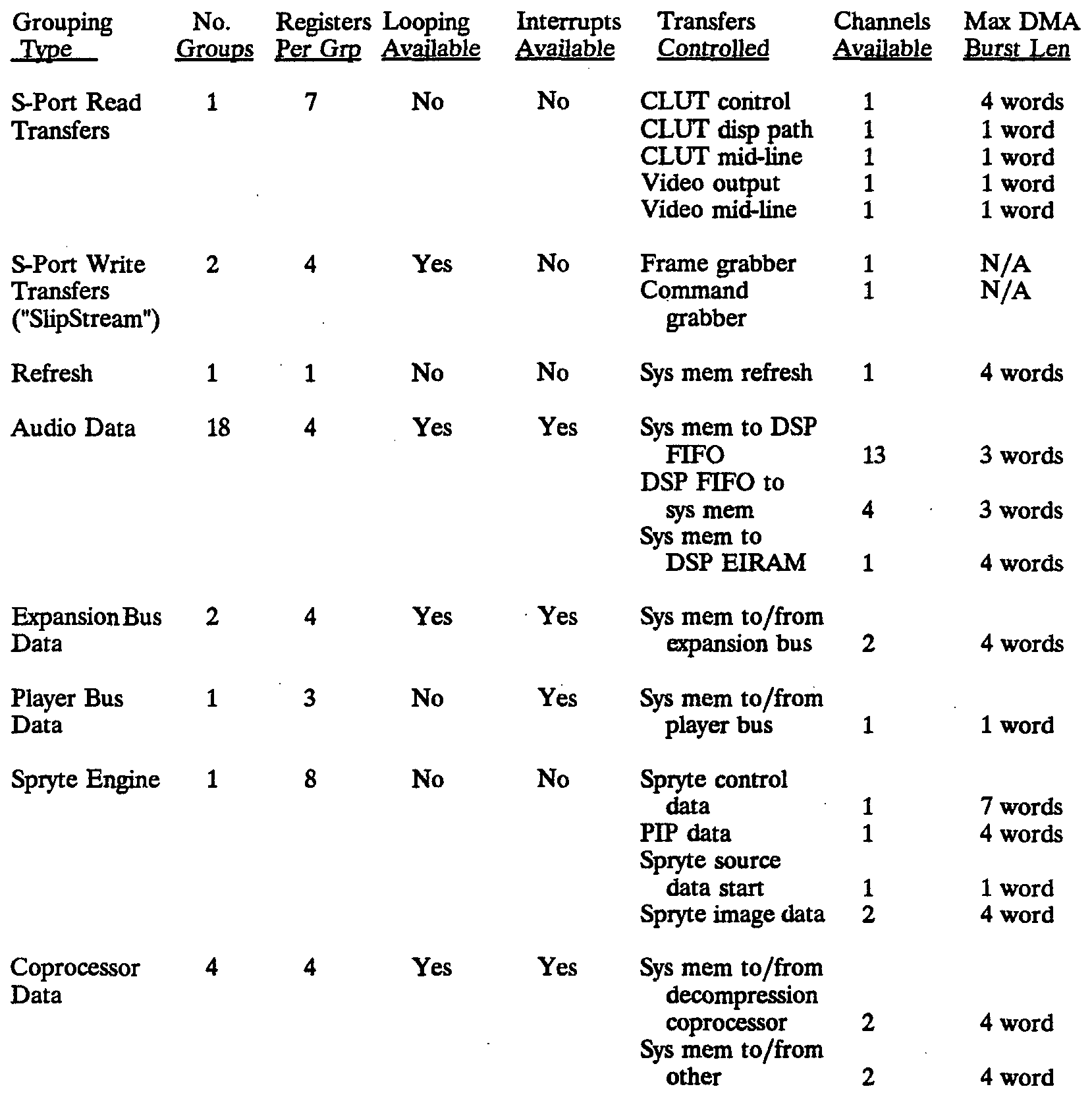
A. Audio Data Groups
An audio data group consists of four DMA stack registers for holding a current address, a remaining length, a back-up address (next starting address) and a back-up length (next starting length) . Typically prior to an audio data transfer to or from the audio subsystem in audio/video processor 140, the CPU 102 will write the starting address and desired length of transfer into the current address and remaining length registers for the
desired channel in DMA stack 312. These registers are all addressable by the CPU 102 as memory-mapped hardware registers. For transfers from system memory to an audio subsystem input FIFO, the address to be written into the DMA stack register for the desired grouping is the system memory source address. For data to be read from an audio subsystem output FIFO to system memory, the address to be stored in the DMA stack register for the grouping is the system memory destination address. The audio subsystem has 13 data input FIFOs and four data output FIFOs, each of which are referred to as a separate channel, and each of which corresponds to a different one of the audio data groupings in the DMA stack 312. Thus, the CPU 102 specifies a particular source or destination FIFO merely by choosing the corresponding audio data grouping in the DMA stack 312.
For transfers from system memory directly to desired addresses in an EIRAM which is internal to the audio subsystem, the 32-bit words to be transferred from system memory are each divided into fields containing the data to be written to EIRAM (typically 16 bits wide) , the DSP internal EIRAM address to which data is to be written, and control information for the particular word transfer. When a current address is written by the CPU 102, the address generator 208 automatically sets the next starting address register for that group to zero in the next clock tick. When the CPU 102 writes a value to the remaining length register of a group, the address generator 208 automatically sets the next starting length register to zero in the next clock tick. These values of zero are used as control flags. The DMA operation is not allowed to be pointed at system memory
at address zero, nor is it allowed to have a length of zero.
The audio subsystem is part of the audio/video processor 140, so all requests for DMA transfers reach the arbiter 210 over the single DMAREQ line previously described. This request includes the desired channel number. When the arbiter 210 grants control of the D- bus and address generator to the audio/video processor 140 requestor, it provides the DMA group address for the desired channel to stack address logic 336 (Fig. 3) as previously described. The DMA group address is passed by multiplexer 402 (Fig. 4) to the registers 404 and 406. The read address for DMA stack 312 is then assembled as the high-order five bits from register 404, and the low-order two bits from register 406. For audio data transfers, the low-order two bits are zero. Accordingly, the read address provided to the DMA stack 312 now points to the first register in the 4-register grouping for the particular audio channel. The contents of this register, which represents the system memory starting address, are read out of the DMA stack 312 and selected by source multiplexer 314 onto the source mux out bus 370. The address is transmitted- via left and right address pad logic 345 and 353 to the left and right bank address buses of system memory 108, respectively, in a manner similar to that for CPU- originated addresses and spryte destination addresses described above. The external processor interface 220 (Fig. 2) of address manipulator 106 drives the appropriate CCODE onto control bus 138 to indicate to audio/video processor 140 that the DMA transfer which it requested is now taking place. For transfers from system memory to the audio subsystem, system memory 108 drives a word of data from the selected address onto the
D-bus 118, 120, and audio/video processor 140 latches in the data from D-bus 118, 120 and internally routes it to the requesting FIFO or EIRAM address. For transfers from the audio subsystem to system memory 108, the audio/video processor chip 140 drives the data from the appropriate audio subsystem output FIFO onto the D-bus 118, 120 and system memory 108 stores it at the selected address.
In addition to being provided to the address lines of system memory 108, the address information on the source mux out bus 370 (Fig. 3) is also captured in register 318, incremented by adder/clipper 320, and written back to the same address in DMA stack 312 via multiplexer 310. The write address for DMA stack 312 comes from register (Fig. 4) which previously derived it from the registers 404 and 406, via the lower input port of multiplexer 408. The read address for DMA stack 312 is now formed by the high-order 5 bits from register 404 (Fig. 4) and the low order 2 bits selected by multiplexer 412 from the control unit 368. At this time, control unit 368 provides '01' of the low-order 2 bits, since the length indication is stored in the second register in the group. DMA stack 312 is dual- ported, so reads and writes to different registers in the DMA stack 312 may be accomplished simultaneously. The length indication, which for audio groups indicates the number of words to be transferred, passes through source multiplexer 314 to register 318, and is decremented by adder/clipper 320 and written back to the same location in the grouping in DMA stack 312. Similarly to the writeback of the incremented starting address, the write address for the decremented length indication is provided by register 410 (Fig. 4), having previously been derived from register 404 and control
lines from control circuitry 368 via the upper input port of multiplexer 408.
If the length as decremented is positive, then the address generator 208 causes the next data word to be transferred in the same manner as the first. Words are transferred in this manner until the maximum contiguous burst length is reached (either three or four words- see Table I), or the length indication as decremented is zero. Some time prior to the completion of this data transfer, if desired, the CPU 102 may write a backup address and a backup length into the third and fourth registers of the audio group. Typically, this is done before the data transfer begins. When the value in the remaining length register becomes zero, the access is completed and a "loop test" is performed. According to the loop test, if the next starting address register is zero, the DMA transfer has completed. If the next starting address value is non-zero, then it is copied to the current address register for the group and the next starting length value is copied into the remaining length register. Such copying occurs via the source multiplexer 314, register 318, adder/clipper 320, and multiplexer 310. The appropriate read and write stack addresses are generated by the control circuitry 368 through the stack address logic 336. The address generator 208 then continues the DMA transfer in the same manner as set forth above with respect to the original transfers specified for the group. This process repeats until the CPU 102 writes a zero into the next starting address register of the particular audio grouping.
DMA looping can be achieved in this manner. Looping is useful, for example, to send a cyclical series of
audio samples to the audio subsystem to have it generate a tone having a particular frequency. Looping action in a DMA transfer always causes a page break (causes address generator 208 to establish a new page address), whether or not the loop is successful.
As can be seen from Table I, DMA transfers are usually in bursts of three or four. For transfers which involve the audio/video processor 140 (audio data transfers, expansion bus transfers and co-processor data transfers), as previously mentioned, address manipulator 106 provides a CCODE on control bus 138 to inform the audio/video processor 140 of the current status of a DMA process that is currently active. A CCODE is sent for each data word transferred, and the audio/video processor 140 responds to each such CCODE either by driving data onto the D-bus or by latching data from the D-bus. Additionally, one bit of information in the CCODE further indicates that the current length register decremented to zero during this burst, and that the DMA channel will now loop. The CCODE also contains a bit of information which indicates that the current length register decremented past zero during this burst, and the next starting address register is already at zero. This means that the DMA channel is not going to loop and the entire specified transfer is complete.
B. Ex ansion BUS Data and Co-Processor Data
Groupings The DMA channels for data transfer between system memory 108 and the expansion bus 142, as well as the DMA channels for transfers between system memory 108 and either the decompression co-processor 166 or another external co-processor (not shown) , all operate similarly to the audio data channels. Looping is performed in a
similar manner, and since the expansion bus interface is a requestor from within the audio/video processor 140, the CCODEs generated by address manipulator 106 are also the same. The decompression co-processor 166 is not strictly within the audio/video processor 140, but it makes its DMA requests through the DMA requestor in audio/video processor 140 and is therefore handled in the same manner. The same is true with respect to an external co-processor. The decompression co-processor 166 and the external co-processor are coupled to the control bus 138 and therefore receive CCODEs directly.
C. S-Port Read Transfers
The DMA stack 312 contains one 8-register group (only seven of which are used) to control read transfers out the S-port of VRAM in system memory 108. The S-port transfers themselves do not require control of the D-bus or the address generator 208, but S-port activity can be controlled only via commands issued over the D-bus. The registers in the group are set forth in Table II.
TABLE II
0 Current CLUT Address 1 Next CLUT Address
2 CLUT Mid-Line Address
3
4 Previous Line Video Address
5 Current Line Video Address 6 Previous Line Mid-Line Address
7 Current Line Mid-Line Address
In order to coordinate control of the video display path with the display scanning operation, the system of
Fig. 1 transmits all of such commands down the display path during an allocated portion of each horizontal blanking period. In particular, about 50 words of
transfer time are allotted during each horizontal blanking period. These commands are mostly directed to the color look-up table (CLUT) , thereby permitting the CLUTs (there are three CLUTs for a scan line — one for each primary color) to be updated each scan line. The use of the commands ("color words") by the CLUTs, and the structure of the CLUT system, are described in the related METHOD AND APPARATUS FOR UPDATING A CLUT DURING HORIZONTAL BLANKING application. Other commands ("control words") are directed to the interpolation mechanism, described in the related RESOLUTION ENHANCEMENT FOR VIDEO DISPLAY USING MULTI-LINE INTERPOLATION application. Still other control words are directed to the audio/video output circuitry 152 (Fig. 1), and are passed by the audio/video processor 140 to audio/video output circuitry 152 over the AD bus 158. Note that in another embodiment, other otherwise unused slots on the S-bus may be used to transmit commands down the video display path, such as during start-up and/or during vertical blanking.
Control registers in audio/video output circuitry 152 are write-only, and are handled completely in the CLUT list transfer process. There is no direct access, from the CPU 102 to the registers in audio/video output circuitry 152, nor can any of such registers be read by the system.
The control words to be transmitted down the video display path during the allocated portion of the horizontal blanking period are prepared in advance by the CPU 102 in the form of a linked list set up by the CPU in VRAM. Although the control words are not always intended for the CLUTs, this list is sometimes referred to herein as a CLUT list. A CLUT list contains four mandatory control words, optionally followed by a
sequential list of up to about 50 command words. The structure of the words in the CLUT list is as follows:
CLUT DMA control word
3 bits select a display mode (320, 384, 512 or 1024 pixels per scan line)
1 bit enables Slip Stream capture during horizontal blanking
1 bit enables the video DMA function
1 bit selects the frame-grabber or the command- grabber DMA slipstream channel
1 bit sets a video mode for the upcoming scan lines to indicate whether 240 or 480 pixels will be provided
1 bit indicates whether the "next CLUT list address" is absolute or relative
1 bit specifies whether the "previous line video address" for subsequent scan lines is to be calculated by adding a modulo or by re-using each previously used "current line video address" 1 bit indicates the validity of the "current line video address" below (0 means re-use the prior "current line video address")
1 bit indicates the validity of the "previous line video address" below (0 means re-use the prior "previous line video address")
6 bits indicate the length in words of this list (minus 4)
9 bits indicate the number of scan lines to wait before processing the next CLUT list
Current Line Video Address
Physical address from which to begin fetching "current" line pixel data after processing this CLUT list.
Previous Line Video Address
Physical address from which to begin fetching "previous" line pixel data after processing this CLUT list.
Next CLUT List Address
Address from which the next CLUT list should be fetched, after the number of scan lines specified in the CLUT DMA control word have been transmitted.
Immediately following the above four control words is a contiguous sequence of up to 50 color and/or control words. Color words are indicated by a zero in bit 31. Eight bits of the word carry a red color value, eight bits carry a green color value, and eight bits carry a blue color value. Five bits of the word indicate the CLUT address to which this color data is to be written (the pen number), and two bits indicate whether to write red only, green only, blue only or all three colors at the indicated pen. Accordingly, by appropriately preparing the CLUT list, it is possible for the software running on CPU 102 to update individual color values for each of the 32 pen numbers in each of the three colors represented in the CLUT. 32 color control words are required to update the entire CLUT. As explained in more detail in the related METHOD AND APPARATUS FOR UPDATING A CLUT DURING HORIZONTAL BLANKING application, the CLUT which is modified by these color control words is the CLUT which is used to translate "current line" pixel data. The CLUT which is used to translate "previous line" pixel data is always updated in its entirety from the "current line" CLUT after each scan line.
If bit 31 of a color/control word is one, and if bit 30 is zero, then the word contains control information for the audio/video output circuitry 152. The audio/
video processor circuitry 140 receives this word over the S-bus 122, and forwards it to the audio/video output circuitry 152 for processing.
If bits 31 and 30 are both one, and if bit 29 is zero, then the word is a display control word and contains the following information:
Display Control Word 1 bit forces audio/video processor 140 to send a null control word to audio/video output circuitry 152
1 bit selects the NTSC or PAL transmission standard
1 bit enables CLUT bypass—see related application
1 bit enables a "surprise" 640 display mode 1 bit forces transparency always, letting overlay data be displayed from slipstream capture
1 bit enables the background color detector in the display path to indicate transparency
1 bit enables random number generator for the three LSBs of CLUT bypass
1 bit enables a window MSB replication gate
1 bit requests a single line disable of vertical interpolation
1 bit swaps the meaning of the horizontal and vertical subposition bits
2 bits select the vertical subposition bit source from: 0, 1, use frame buffer bit, and maintain prior setting
2 bits select the horizontal subposition bit source from: 0, 1, use frame buffer bit, and maintain prior setting 2 bits select the blue pen LSB source from: 0, use frame buffer data bit 0, use frame buffer data bit 5, and maintain prior setting
1 bit enables vertical interpolation
1 bit enables horizontal interpolation 9 bits have the same meaning with respect to a window within the display field, as the last- mentioned 9 bits have with respect to the remainder of the display. The window is described in the related APPARATUS AND METHOD FOR UPDATING A CLUT DURING HORIZONTAL
BLANKING application.
If bits 31, 30 and 29 of a color/control word are all one, then the word contains three 8-bit color fields (red, green and blue) for writing to the "background" pen of the CLUTs.
During initialization, the CPU 102 writes the address of a "top of field" CLUT list into register 1 (next CLUT address) of the S-port read transfer group in DMA stack 312. If enabled, the top of field CLUT list is initiated every field by the CLUT control circuitry near the end of scan line 5 (or 4, depending on which field is being generated) . To initiate the action, S-port control circuitry 224 of the address manipulator chip 106 (Fig. 2) issues a request to arbiter 210. When granted, the arbiter 210 transmits the DMA group address for S-port read transfers to the stack address logic 336 in the address generator 208. Stack address logic 336 generates the stack address of the 8-register S-port read grouping to the read address input of DMA stack 312, and source multiplexer 314 drives the top of field CLUT address from register 1 of that DMA stack register grouping onto the source mux out bus 370. The top-of-field CLUT address is also copied into register 0 of the group to indicate the current CLUT address. In the manner previously described with respect to audio data transfers, the top of field CLUT
address is provided to the left and right memory banks 108A and 108B, which in turn drive the first word of the CLUT list (i.e., the DMA control word), onto the D-bus 118, 120. The address manipulator chip 106 receives the word onto its MDT data bus 202 via the buffers 222 (Fig. 2) and provides it to the S-port control circuitry 224. Appropriate bits are set in the S-port control unit 224 in response to the settings in the control word. Additionally, the CLUT list length indication from the control word is loaded into a word counter (not shown) , and the number of scan lines to wait before processing the next CLUT list is loaded into a scan line counter (not shown) .
Address generator 208 automatically increments the system memory read address from register 0 of the group in the manner previously described, using adder/clipper 320, register 324 and multiplexer 316 providing the output of register 324 through the source multiplexer 314 back onto the source mux out bus 370. System memory 108 accordingly then drives the second word of the CLUT list onto the D-bus 118, 120. This value represents the address from which to begin fetching "current" line pixel data for the current scan line. Referring to Fig. 3, bits 23:2 of this address are taken from the MDT data bus 202 and provided to the DMA stack input port 312 via multiplexers 308 and 310. The address generator control circuitry 368 provides appropriate control signals to the stack address logic 336 (Fig. 4) such that this information will be written into register 5 of the S-port read transfer group, the current line video address register.
The address generator 208 then increments the address provided to system memory 108 again, such that system memory 108 drives the third word of the CLUT list
onto D-bus 118, 120. This information, representing the address from which to begin fetching "previous" line pixel data, reaches the data input port of DMA stack 312 in the same manner as did the current line video address. Address generator control circuitry 368 controls the stack address logic 336 to provide the address of register 4 of the S-port read transfer group to the write address input of the DMA stack 312, so that this information may be written to register holding the previous line video address. In a similar manner, the fourth word of the CLUT list, representing the address of the next CLUT list, is written into register 1 of the S-port read transfer register grouping of the DMA stack 312, overwriting the top-of-field CLUT list address. After these four transfers take place, if the CLUT DMA control word indicated a non-zero number of color/display path control words to follow, address generator 208 initiates a CLUT list display path transfer. In particular, address generator 208 drives the value in current CLUT address register 0 of the S- port read transfer grouping in DMA stack 312, onto the left and right address buses of system memory 108, and S-port control circuitry 224 drives appropriate control signals to both banks of VRAM to cause a full read transfer of the page of the specified address into the static holding register. (See the above-mentioned NEC Datasheets.) The S-port control circuitry 224 also loads the column address into the left and right bank VRAM as the starting tap for shifting purposes. Address generator 208 also at this time uses the adder/clipper 320 to calculate the next page address which will have to be written to the VRAMs, and stores this in register 2 ("CLUT mid-line address") of the S-port read transfer address grouping in DMA stack 312. The S-port control
circuitry 224 then issues the appropriate number of serial clocks to the left and right banks of VRAM in system memory 108, to transmit the entire list of color/display path control words over the S-bus and down the video display path. During this time the D-bus is free to service other requestors.
After the CLUT mid-line address is calculated, a CLUT mid-line request is issued automatically to the D-bus arbiter 210, whether or not it is needed. Note that a second mid-line request for a CLUT transfer will never be needed since a CLUT list can never be more than 64 words long whereas a half-page of the VRAM is 256 words long. When the D-bus is granted for the automatic CLUT mid-line request, address generator 208 provides the CLUT mid-line address from register 2 of the S-port read transfer grouping, for issuing the split read transfer command to the VRAMs. S-port control circuitry 224 continues issuing serial clocks to the left and right banks of VRAM until all the words of color/display path control have been transmitted. The D-bus and address generator 208 are available for other uses during this time.
Shortly before the end of the horizontal blanking period, S-port control circuitry 224 issues a start video request to the arbiter 210. When granted, the address generator 208 latches the "previous line video address" from register 4 of the S-port read transfer grouping, into the registers 348 and 356. PFL logic 366 determines whether the previous line pixel data will come from the left or right bank of VRAM, depending on various system conditions. In either case, S-port control circuitry 224 applies the appropriate signals to the appropriate VRAM to have an initial full read transfer performed and the appropriate column number
written into the VRAM as a starting tap. Similarly, the "current line video address" from register 5 of the S- port read transfer grouping is used to perform an initial full read transfer and to set the starting tap of the opposite bank of VRAM. The address generator 208 also at this time calculates the next half-page address for previous line pixel data and stores it in register 6 of the S-port read transfer grouping, and calculates the next half-page address for current line pixel data and stores it in register 7 of the S-port read transfer grouping in DMA stack 312. The D-bus and address generator 208 are then released to service other requestors, and S-port control circuitry 224 issues the proper serial clocks to the VRAMs to transmit previous and current line pixel data over the S-bus and down the video display path.
Previous and current mid-line requests are issued in response to LQSF and RQSF with the previous and current line mid-line addresses stored in registers 6 and 7 of the S-port read transfer grouping in DMA stack 312 being updated each time with an incremented half-page address.
After the number of horizontal scan lines specified in the CLUT DMA control word complete, and when the portion of the horizontal blanking period allocated to CLUT list transfers arrives, S-port control unit 224 issues a request to arbiter 210 for control of the D-bus and address generator 208. When granted, the S-port transfer of the next CLUT list begins in the same manner set forth above. If the number of scan lines to wait before loading the next CLUT list is zero, then S-port control 224 no longer checks for new transfer requests until the next "top of field" occurs. The top of field CLUT list transfer will take place beginning with the address specified in register 1.
D. DMA Stack Register Grouping for System Memory
Refresh The refresh address is held in a single DMA stack location. Whenever the horizontal scan line count reaches a predefined pixel position, four requests are made to arbiter 210 for system memory refresh operations. The four requests are independent and are handled as separate requests. When a refresh request is granted, arbiter 210 provides the DMA group address of the refresh counter to stack address logic 336, which reads the current refresh address onto the source mux out bus 370. The address is loaded into both registers 348 and 356 and the left and right pad address logic 345 and 353 each select the low-order bits for driving onto the address buses 110 and 114. Address generator 208 then issues the appropriate RAS and CAS signals to both memory banks to thereby refresh the system memory page pointed to by the low-order bits of the refresh address. The refresh address is then incremented by adder/clipper 320 and written back into the refresh address register in DMA stack 312.
E. Player Bus DMA Register Grouping
The register grouping in DMA stack 312 for transfers between system memory and the player bus contains three registers: the system memory write address, the system memory read address, and the length of transfer in words. As previously mentioned the player bus uses a single stream serial protocol that is run at a rate of once per display field. Details of the player bus and the serial protocol may be found in the related PLAYER BUS APPARATUS AND METHOD application. When the display is on scan line 17, if the player bus DMA channel is
enabled, player bus control 504 (Fig. 5) makes a request to arbiter 210 for control of the D-bus and the address generator 208. When granted, the address generator 208 will first read the contents of the 32-bit player bus shift register 502 and transfer it to the address in system memory 108 specified by the system memory write address register in the player bus grouping of the DMA stack 312. Note this first word contains information shifted in at the end of the previous stream and is therefore irrelevant and should be ignored by the software. The address generator 208 then transfers a 32-bit word from the system memory 108 address specified by the system memory read address register in the player bus grouping of DMA stack 312, to the shift register 502. Address generator 208 also increments the addresses in the system memory write address register and system memory read address register of the player bus grouping in the DMA stack 312, and decrements the length register in such grouping. The player bus control unit 504 then simultaneously shifts out the 32 bits from the shift register 502 onto the player bus, and shifts in 32 new bits of data from the player bus into the shift register 502. At the completion of the shift, player bus control unit 504 again requests control of the D-bus and address generator 208 for another pair of DMA transfers to and from system memory 108. Accordingly, the DMA address and length registers for the player bus channel operate in the same fashion as those for the audio DMA channels described above, except that looping is not enabled. The size of the shift register 502 is only one word, so the transfer burst size in each direction is only one word.
Note that software running on CPU 102 needs to re- enable the player bus DMA channel once each display
field. This takes place automatically when the CPU 102 writes a value into the length register of the player bus register grouping in DMA stack 312. The channel is automatically disabled when the length register reaches zero. The channel may also be programmed to interrupt the CPU 102 when the length register reaches zero.
The useful length of the output stream and the input stream on the player bus are not directly related. Either one may be longer. Since one clock is used for both streams, non-valid input data could arrive and must be ignored. Additionally, the output stream may need to be padded with leading zeros. Also, note that disablement of the player bus DMA channel and interruption of the CPU 102 when the length register decrements to zero, merely indicates that all necessary DMA transfers have taken place; player bus control 504 still must shift the word most recently transferred to shift register 502, out the player bus.
F. Spryte Engine Data Transfers
In order to render a spryte into an area of system memory 108, the CPU 102 first sets up the required data in a different area of the system memory 108. Such data includes 6 to 15 32-bit words as specified in Table II above, all located contiguously in system memory 108; 4, 8 or 16 optional 32-bit words contiguously located in system memory 108 to represent PIP data; and spryte image data of any length. Of the 6 to 15 words specified in Table II, note that several groups are optional as set forth more fully below. Note also that the second word of the SCoB is a pointer to the next SCoB to process; thus, the CPU may create a linked list of any number of SCoBs to process in sequence, each
defining its own spryte source data, optional PIP data, and spryte rendering control information.
Also prior to starting the spryte engine, the CPU 102 writes desired information directly into certain memory-mapped hardware registers as follows:
SCOBCTL0. 32-bit word defined in Table III below.
XΔBLEJH SCOBCTLO Engine Control Word
Bits Namft PeSCri tion B31:B30 = B15POS B15 oPEN selector for output of PMPP. (This bit can function as a subposition defining bit that is used by the pre-display interpolater.) 0=0, 1=1, 2=xx, 3= same as Source data
B29:B28 = BOPOS B0 oPEN selector for output of PMPP. (This bit can also function as a subposition defining bit that is used by the pre-display interpolater.) 0=0, 1=1, 2=PPMP math, 3= same as Source data
B27 = SWAPHV l=Swap the H and V subpositions prior to their entry into the
PPMP
B26 = ASCALL 1= Allow super clipping function (master enable switch)
B25 = xx Reserved B24 = CFBDSUB 1 = use the H and V subposition bits of the cFB data in place of
(vice) the spryte source values when the cFB data is selected as a PPMP source. (Note: CFBDsel=(Sl=l) OR (S2=2).)
B23:B22 = CFBDLSB cFBD PPMP Blue LSB source. 0=0, l=cFBD[B0], 2= cFBD[B4], 3=x
B21:B20 = IPNLSB IPN PPMP Blue LSB source. 0=0, 1=IPN[B0], 2=IPN[B4], 3=x
Note that when 'relative' has been specified in the flags for NEXTPTR, SOURCEPTR, or PIPPTR, the value that should (must) be placed in the SCoB is the word distance from the address in RAM that has the relative value in it to the address in RAM that is desired to be the new address MINUS FOUR. (REL= Target - PC - 4). Also note that the BOPOS value of - 2 ' is the only setting that
uses PPMP math to control the BO bit in the actually output oPEN signal. When this setting is chosen, the Blue LSB will also be included in the input parameters of the black detector. REGCTLO. Controls the modulo for reading source frame buffer data into the primary and/or secondary input port of the spryte engine 214 and for writing spryte image result data from the spryte engine 214 into a destination frame buffer in system memory 108. The modulo effectively indicates the number of pixels per scan line as represented in the respective frame buffer in system memory 108.
Only the low-order 16 bits of REGCTLO are used. The low-order 8 bits specify the modulo for the source frame buffer, and the next 8 bits specify the modulo for the destination frame buffer. For each of the two modulo designations, the low-order 4 bits specify a Gl value and the high-order 4 bits specify a G2 value. The modulo specified for a particular buffer is then calculated as G1+G2. Thus the following bits of REGCTLO are defined (CFBD refers to current frame buffer data, a source buffer separate from spryte source data, which the spryte engine may read as input data) :
REGCTLO BIT DESCRIPTION
0 Gl=32 for CFBD read buffer.
1 Undefined. Set to 0.
2 Gl=256 for CFBD read buffer.
3 Gl=1024 for CFBD read buffer. 4 G2=64 for CFBD read buffer.
5 G2=128 for CFBD read buffer.
6 G2=256 for CFBD read buffer.
7 Undefined. Set to 0.
8 Gl=32 for destination buffer. 9 Undefined. Set to 0.
10 Gl=256 for destination buffer.
11 Gl=1024 for destination buffer.
12 G2=64 for destination buffer.
13 G2=128 for destination buffer.
14 G2=256 for destination buffer.
15 Undefined. Set to 0.
The software must ensure that no more than one bit in each nibble is set. The hardware does not protect against setting more than one bit. If no bits are set in a nibble, the contribution to the resultant modulo is zero.
REGCTL1. X and Y clip values, effectively indicating the number of pixels in the X and Y dimensions which make up the frame buffer. Bits 26:16 indicate the last writeable row (counting from row 0) in the Y dimension and bits 10:0 indicate the last writeable column (counting from col. 0) in the X dimension. All other bits must be zero. As an example, a value of 00EF013F indicates that the frame buffer data is represented in 320x240 format.
REGCTL2. Read base address. Indicates the address in system memory 108 of the upper left corner pixel of the source frame buffer data.
REGCTL3. Write base address. Indicates the address in system memory 108 of the upper left corner pixel of the destination frame buffer (CFBD) .
Also before the spryte engine is started, the CPU 102 places the address of the first SCoB in the linked list into the DMA stack 312 register corresponding to "next SCoB". The CPU then writes to the memory mapped address designated SPRSTRT in order to start the spryte engine running. Once the spryte engine starts running, it retains exclusive control of the D-bus until either it finishes processing all the SCoBs in the list, or an interrupt occurs. If an interrupt occurs, the spryte engine continues to a convenient stopping point, then releases the D-bus. The CPU then vectors to an appropriate interrupt handler, and when done, returns to
the routine which originally started the spryte engine. That routine checks the status bit SPRON in a memory mapped status bit register to determine whether the spryte engine stopped due to an interrupt or due to completion of processing, and if the former, restarts the spryte engine. In an alternative embodiment, the CPU can have a separate bus to program memory, to thereby permit the CPU 102 to perform other tasks while the spryte engine 214 renders the sprytes. In the latter embodiment, the spryte engine can generate an interrupt for the CPU 102 when spryte processing has completed, at which time the CPU 102 can vector to an interrupt handler.
The DMA stack 312 includes an 8-register grouping for spryte control. The eight registers are as follows:
0 CURRENT SCOB ADDRESS
1 NEXT SCOB ADDRESS
2 PIP ADDRESS
3 SPRYTE DATA ADDRESS 4 ENGINE A FETCH ADDRESS
5 ENGINE A LENGTH
6 ENGINE B FETCH ADDRESS
7 ENGINE B LENGTH When the CPU writes to the SPRSTRT address, after the spryte engine gains control of the system data bus 118, 120, the DMA engine of Figs. 3 and 4 loads in the first six words from the first SCoB beginning from the system memory address specified in the NEXT SCOB register in the DMA stack 312. To accomplish this, the address of the first word to load is read out of the NEXT SCOB register and provided to the memory address lines via source multiplexer 314. The address is also incremented by adder/clipper 320 and written back via multiplexer 310 into the CURRENT SCOB register in DMA stack 312. All six words are read from memory in this
manner, the CURRENT SCOB register maintaining the address of each next word to load.
The first SCoB word read, FLAGS, is written into a 32-bit hardware register in address manipulator chip 106. The next SCoB word read, NEXTPTR, is written into the NEXT SCOB register in DMA stack 312. SOURCEPTR is written into the SPRYTE DATA ADDRESS register of DMA stack 312, and PIPPTR is written into the PIP ADDRESS register in DMA stack 312. XPOS and YPOS are written to two memory mapped hardware registers XYPOSH and XYPOSL, each having the format of x,y. That is, the high-order 16 bits from XPOS and the high-order 16 bits from YPOS are written to the high- and low-order half words, respectively, of XYPOSH, and the low-order 16 bits of XPOS and the low-order 16 bits of YPOS are written to the high and low half words, respectively, of XYPOSL.
After the first six words of the SCoB are loaded, depending on the bits which were set in FLAGS, up to seven additional SCoB words are loaded. The possible words are grouped as a single DMA transfer of up to seven words. If the LDSIZE bit of FLAGS was asserted, then the DMA controller of Figs. 3 and 4 expects the first four words of this group of seven to be DX, DY, LINEDX and LINEDY. These words are loaded in the same manner as the first six words of the SCoB, the incremented addresses being stored in the CURRENT SCOB register in DMA stack 312. DX and DY are written in x,y format into two memory mapped hardware registers DXYH and DXYL, and LINEDX and LINEDY are written in x,y format to two memory mapped hardware registers DDXYH and DDXYL. Note that if the SKIP bit of the FLAGS word equals one, indicating that the present SCoB is to be skipped, or if the YOXY bit is zero, then the X and Y values are not written to the hardware.
If the LDPRS bit of FLAGS was set, then the DMA control unit of Figs. 3 and 4 expects the first two words (or the next two words) of the optional seven to contain DDX and DDY. These are written in x,y format to two memory mapped hardware registers DDXYH and DDXYL.
If the LDPPMP bit of the FLAGS word was set, then the DMA control unit of Figs. 3 and 4 expects the first (next) word of the optional seven words to be PPMPC. This word is written to a memory mapped PPMPC hardware register.
After the second SCoB load of zero through seven words, the DMA control unit of Figs. 3 and 4 performs a preamble load of either one or two words. If the SCOBPRE bit of FLAGS was set, then the preamble word(s) is (are) assumed to be at the end of the SCoB, in which case the CURRENT SCOB register in DMA stack 312 contains the address of the first preamble word. If SCOBPRE was not set, then the preamble word(s) is (are) assumed to be at the start of the data, in which case the SPRYTE DATA ADDRESS contains the address of the first preamble word. The DMA control unit selects the appropriate register source for the starting address of the preamble load and returns the incremented addresses to the same register. The first preamble word is always present and is loaded into the appropriate hardware registers. The second preamble word is present only when the PACKED bit of the FLAGS word was zero, indicating that the spryte image data is in "totally literal" format. When the DMA unit reads this word, the information in the WOFFSET field is written to an offset register and the information in the TLHPCNT field is written to a pixel count register in the hardware. The offset indicates the width of the totally literal spryte in memory, and
is used by the DMA controller to calculate the start of each next line of the spryte source data. The pixel count indicates the number of pixels to be transferred on each scan line of totally literal spryte source data. These two values are settable independently in order to permit the transfer of only a rectangular portion of a larger bit image, smaller than the overall bit image both in width and height.
After the preamble load, if the LDPIP bit of the FLAGS word was set, the DMA control unit will read out 4, 8 or 16 words of PIN to IPN conversion information, beginning from the address in the PIP ADDRESS register in the DMA stack 312. Incremented addresses are also rewritten into the same DMA stack register. The number of 4-word bursts to perform (if any) depends on the data compression format of the spryte image source data, which is specified in the BPP ("bits per pixel") field of the first preamble word. In particular, as set forth in Table VIII of the related METHOD FOR CONTROLLING A SPRYTE RENDERING PROCESSOR application, a total of four PIP words will be loaded for BPP = 0, 1 or 2; eight PIP words will be loaded if BPP = 3; and 16 PIP words will be loaded if BPP = 4, 5, 6 or 7. Note that since PIP. data in system memory 108 is referenced indirectly, the same PIP data may be downloaded from multiple SCoBs. Also, the PIP may be loaded even if it will not be used to decompress the current spryte image source data (which is the case if the LINEAR bit of the first preamble word is one). For loads of all 16 PIP words, the entire PIP is overwritten. For loads of fewer than 16 words, the PIPA field of the FLAGS word indicates the starting address in the PIP for receiving the data.
After the PIP load, the DMA unit of Figs. 3 and 4 begins transferring spryte image source data from system
memory 108 to the data input FIFOs of the spryte engine 214. As set forth above, if the spryte image source data is packed (i.e. not in totally literal format), then at the beginning of each scan line of spryte source data, the first one or two bytes of the first word contain a word offset from the start of the current line of source data to the start of the next line of source data, minus 2. This offset is used by the DMA controller both to calculate the start of each next line of source data and to set the length of a DMA transfer of the line of source data. Accordingly, the DMA controller reads this word from the address specified in the SPRYTE DATA ADDRESS register of the DMA stack 312, incrementing the address and placing it into the ENGINE A FETCH ADDRESS register of the DMA stack 312. The high-order 8 or 10 bits of this word are placed into the ENGINE A LENGTH register of the DMA stack 312, and the entire word is also sent to the spryte engine data input FIFO for corner engine A. The spryte engine knows to ignore this word. Note that if the spryte image source data is in totally literal format, then the single offset value (as well as the pixel count value) specified in the second preamble word and described above applies to the entire spryte. After the offset is loaded, the DMA controller then transfers additional words of spryte image source data for the current scan line in bursts of up to four words each, as requested by the spryte engine 214. The starting address for each burst is found in the ENGINE A FETCH ADDRESS register of DMA stack 312, and the incremented addresses are placed in the same register. Correspondingly, the DMA controller decrements the value in the ENGINE A LENGTH register of DMA stack 312 according to the number of words transferred.
The DMA controller also updates the SPRYTE DATA
ADDRESS register in DMA stack 312 by adding the offset specified in the first word of the scan line, so that that register always points to the next scan line to be processed.
Note that on the conditions described in the above- mentioned SPRYTE RENDERING SYSTEM WITH IMPROVED CORNER CALCULATING ENGINE AND IMPROVED POLYGON-PAINT ENGINE APPLICATION, the spryte engine 214 can also request DMA transfers of 4-word bursts of the next scan line of spryte image source data into the corner engine B data input FIFO, using the ENGINE B FETCH ADDRESS and ENGINE B LENGTH registers. In this manner, both corner engines A and B in the spryte engine 214 can operate on different scan lines of spryte image source data simultaneously, and the DMA controller can burst data to each as independently requested.
VII. General Operation of the System On release from reset, the address manipulator chip 106 maps the CPU ROM 132 into the bottom of the CPU 102 address range (beginning at address zero) . This range is read only until it is remapped to system memory space during the ROM start-up procedure. The ROM start-up procedure clears all necessary hardware conditions to a predefined state, determines the size of system memory 108 and sets the appropriate hardware bits, and performs various hardware initialization processes. The start¬ up ROM code will also copy ROM code to RAM and instruct the address manipulator chip 106 to remap the address space accordingly.
When a media change event occurs at one of the expansion bus devices, such as the insertion of a new CD into CD/CD-ROM player 148, the device asserts a signal
on expansion bus 142 to expansion bus interface 614. Expansion bus interface 614 sets some hardware bits which have the effect of preventing any commands issued by the hardware from reaching the device which had the media change. Only the CPU 102, running in a supervisor mode, can clear these bits, and it does so as part of a soft reset. An interrupt is sent to the CPU 102, which begins executing a media change routine in the supervisor mode from CPU ROM 132. This routine executes the soft reset to clear the hardware bits. After release from the soft reset, the CPU continues executing the media change routine by accessing the media to determine format and validity. For example, if the CPU 102 determines that a new CD inserted into CD/CD-ROM player 148 is in standard CD/audio format, then the CPU 102 jumps to a routine which automatically causes the CD to be read, passed through audio subsystem 606, converted to analog form by audio/video output circuitry 152, and driven onto the audio left and right output lines (Fig. 1). Alternatively, if the CPU 102 determines that the newly inserted CD is in a standard photo-CD format, then it may jump to a routine which reads it into system memory 108 and writes it out via the S-bus 122, the video display path 618, and audio/video output circuitry 152, to the display.
Still further, if the CPU 102 determines that the new CD is not in one of a set of predefined standard formats, then it is assumed to be a CD/ROM having software for execution by the CPU 102. Such software may be completely or partially encoded, such as by the method of U.S. Patent No. 4,405,829, 4,200,770, 4,218,582 or 4,995,082, all incorporated herein by reference. The CPU 102 determines the authenticity of the data on the disk and copies a table of contents into
system memory 108. Starting software is then located on the disk and retrieved into system memory 108 either by direct CPU byte reads from the expansion interface 614, or by DMA transfers. The software contains instructions intended for execution by the CPU 102, and it may need to be decompressed either by the decompression co-processor 166 (Fig. 1) or by a routine running in the audio subsystem 606, before execution begins. With the exception of some routines which may already be present in system memory 108 (having been copied there from the CPU ROM 132), this software can contain instructions to cause the system of Fig. 1 to perform all of the various user-level multimedia operations described herein.
As previously mentioned, software may be provided to the system of Fig. 1 instead by download via a cable interface to the expansion bus 142. In such a situation, all addresses and procedures described above with respect to CD/ROM originated software can be applied to the cable interface. Still further, as previously mentioned, the software can be downloaded from a cable via the video input device 160, transmitted over the S-bus during the horizontal blanking period, and stored in system memory 108. After authentication procedures are performed thereon, and any required decoding and/or decompression, it may be executed by CPU 102.
The invention has been described with respect to particular embodiments thereof, and it will be understood that numerous modifications are possible within its scope.
Claims
1. A multi-media system for use with a video display, comprising: a CPU; a memory having a parallel port and a serial port, at least said parallel port being read/write, said parallel port being coupled to said CPU over a parallel data bus; a graphics manipulation processor coupled to said memory over said parallel data bus; a video display path coupled between said serial port of said memory and said display; and arbitration means for arbitrating control of said parallel port of said memory from requests issued by said CPU and by said graphics manipulation processor, said graphics manipulation processor having higher priority in said arbitration than said CPU.
2. A multi-media system having a CPU, a memory, a graphics manipulation processor, an audio manipulation processor, and a video output path different from said graphics manipulation processor; and means for loading software into said memory for said CPU to execute, said software including instructions for controlling said graphics manipulation processor, said audio manipulation processor, and/or said video output path.
3. A multi-media system for use with a display, comprising: a memory containing video pixel color information for scan lines to be displayed on said display; a serial data bus coupled to said memory; a video display path coupled to receive said pixel color information in coordination with the timing of said scan lines, over said serial data bus; and means for transmitting control information to said video display path over said serial data bus in coordination with said timing of said scan lines.
4. A method for generating a video image, comprising the steps of: providing a first image description, said first image description including first display position information and first color information for each pixel in said first image, said first color information being in a first compressed format; providing a second image description, said second image description including second display position information and second color information for each pixel in said second image; applying said first image description to said second image description in a predefined transformation to generate a third image description in a memory, said third image description including third display position information and third color information for each pixel in said third image, said third color information being in a third compressed format; and transmitting a dynamically decompressed version of said third image to a display.
Priority Applications (2)
| Application Number | Priority Date | Filing Date | Title |
|---|---|---|---|
| PCT/US1992/009349 WO1994010641A1 (en) | 1992-11-02 | 1992-11-02 | Audio/video computer architecture |
| AU30588/92A AU3058892A (en) | 1992-11-02 | 1992-11-02 | Audio/video computer architecture |
Applications Claiming Priority (1)
| Application Number | Priority Date | Filing Date | Title |
|---|---|---|---|
| PCT/US1992/009349 WO1994010641A1 (en) | 1992-11-02 | 1992-11-02 | Audio/video computer architecture |
Publications (1)
| Publication Number | Publication Date |
|---|---|
| WO1994010641A1 true WO1994010641A1 (en) | 1994-05-11 |
Family
ID=22231496
Family Applications (1)
| Application Number | Title | Priority Date | Filing Date |
|---|---|---|---|
| PCT/US1992/009349 WO1994010641A1 (en) | 1992-11-02 | 1992-11-02 | Audio/video computer architecture |
Country Status (2)
| Country | Link |
|---|---|
| AU (1) | AU3058892A (en) |
| WO (1) | WO1994010641A1 (en) |
Cited By (27)
| Publication number | Priority date | Publication date | Assignee | Title |
|---|---|---|---|---|
| WO1996041279A1 (en) * | 1995-06-07 | 1996-12-19 | Advanced Micro Devices, Inc. | Computer system having a dedicated multimedia engine including multimedia memory |
| WO1997044742A1 (en) * | 1996-05-17 | 1997-11-27 | Advanced Micro Devices, Inc. | Computer system having a multimedia engine coupled to a real-time data cache |
| WO1998011729A1 (en) * | 1996-09-13 | 1998-03-19 | Silicon Graphics, Inc. | Compression and decompression scheme performed on shared workstation memory by media coprocessor |
| US5748983A (en) * | 1995-06-07 | 1998-05-05 | Advanced Micro Devices, Inc. | Computer system having a dedicated multimedia engine and multimedia memory having arbitration logic which grants main memory access to either the CPU or multimedia engine |
| US5748921A (en) * | 1995-12-11 | 1998-05-05 | Advanced Micro Devices, Inc. | Computer system including a plurality of multimedia devices each having a high-speed memory data channel for accessing system memory |
| US5784592A (en) * | 1995-09-11 | 1998-07-21 | Advanced Micro Devices, Inc. | Computer system which includes a local expansion bus and a dedicated real-time bus for increased multimedia performance |
| US5870622A (en) * | 1995-06-07 | 1999-02-09 | Advanced Micro Devices, Inc. | Computer system and method for transferring commands and data to a dedicated multimedia engine |
| EP1145218A2 (en) * | 1998-11-09 | 2001-10-17 | Broadcom Corporation | Display system for blending graphics and video data |
| US6331856B1 (en) | 1995-11-22 | 2001-12-18 | Nintendo Co., Ltd. | Video game system with coprocessor providing high speed efficient 3D graphics and digital audio signal processing |
| US6411301B1 (en) | 1999-10-28 | 2002-06-25 | Nintendo Co., Ltd. | Graphics system interface |
| US6421058B2 (en) | 1999-10-28 | 2002-07-16 | Nintendo Co., Ltd. | Graphics command stream for calling a display object in a graphics system |
| US6580430B1 (en) | 2000-08-23 | 2003-06-17 | Nintendo Co., Ltd. | Method and apparatus for providing improved fog effects in a graphics system |
| US6606689B1 (en) | 2000-08-23 | 2003-08-12 | Nintendo Co., Ltd. | Method and apparatus for pre-caching data in audio memory |
| US6639595B1 (en) | 2000-08-23 | 2003-10-28 | Nintendo Co., Ltd. | Achromatic lighting in a graphics system and method |
| US6643744B1 (en) | 2000-08-23 | 2003-11-04 | Nintendo Co., Ltd. | Method and apparatus for pre-fetching audio data |
| US6664958B1 (en) | 2000-08-23 | 2003-12-16 | Nintendo Co., Ltd. | Z-texturing |
| US6664962B1 (en) | 2000-08-23 | 2003-12-16 | Nintendo Co., Ltd. | Shadow mapping in a low cost graphics system |
| US6697074B2 (en) | 2000-11-28 | 2004-02-24 | Nintendo Co., Ltd. | Graphics system interface |
| US6768774B1 (en) | 1998-11-09 | 2004-07-27 | Broadcom Corporation | Video and graphics system with video scaling |
| US6798420B1 (en) | 1998-11-09 | 2004-09-28 | Broadcom Corporation | Video and graphics system with a single-port RAM |
| US6937245B1 (en) | 2000-08-23 | 2005-08-30 | Nintendo Co., Ltd. | Graphics system with embedded frame buffer having reconfigurable pixel formats |
| US6980218B1 (en) | 2000-08-23 | 2005-12-27 | Nintendo Co., Ltd. | Method and apparatus for efficient generation of texture coordinate displacements for implementing emboss-style bump mapping in a graphics rendering system |
| US7129956B2 (en) | 2000-06-02 | 2006-10-31 | Nintendo Co., Ltd. | Variable bit field color encoding |
| US7369665B1 (en) | 2000-08-23 | 2008-05-06 | Nintendo Co., Ltd. | Method and apparatus for mixing sound signals |
| TWI386863B (en) * | 2008-10-03 | 2013-02-21 | Alpha Imaging Technology Corp | Multi-media processor, hand-held electrical communication device and image processing method thereof |
| US9668011B2 (en) | 2001-02-05 | 2017-05-30 | Avago Technologies General Ip (Singapore) Pte. Ltd. | Single chip set-top box system |
| CN112732603A (en) * | 2019-10-14 | 2021-04-30 | 广州飒特红外股份有限公司 | Multi-channel VDMA control method and application thereof |
Citations (3)
| Publication number | Priority date | Publication date | Assignee | Title |
|---|---|---|---|---|
| US4731742A (en) * | 1984-03-16 | 1988-03-15 | Ascii Corporation | Video display control system |
| US4991120A (en) * | 1989-05-30 | 1991-02-05 | Eastman Kodak Company | Apparatus for interfacing video frame store with color display device |
| US4991122A (en) * | 1987-10-07 | 1991-02-05 | General Parametrics Corporation | Weighted mapping of color value information onto a display screen |
-
1992
- 1992-11-02 WO PCT/US1992/009349 patent/WO1994010641A1/en active Application Filing
- 1992-11-02 AU AU30588/92A patent/AU3058892A/en not_active Abandoned
Patent Citations (3)
| Publication number | Priority date | Publication date | Assignee | Title |
|---|---|---|---|---|
| US4731742A (en) * | 1984-03-16 | 1988-03-15 | Ascii Corporation | Video display control system |
| US4991122A (en) * | 1987-10-07 | 1991-02-05 | General Parametrics Corporation | Weighted mapping of color value information onto a display screen |
| US4991120A (en) * | 1989-05-30 | 1991-02-05 | Eastman Kodak Company | Apparatus for interfacing video frame store with color display device |
Cited By (49)
| Publication number | Priority date | Publication date | Assignee | Title |
|---|---|---|---|---|
| WO1996041279A1 (en) * | 1995-06-07 | 1996-12-19 | Advanced Micro Devices, Inc. | Computer system having a dedicated multimedia engine including multimedia memory |
| US5748983A (en) * | 1995-06-07 | 1998-05-05 | Advanced Micro Devices, Inc. | Computer system having a dedicated multimedia engine and multimedia memory having arbitration logic which grants main memory access to either the CPU or multimedia engine |
| US5732224A (en) * | 1995-06-07 | 1998-03-24 | Advanced Micro Devices, Inc. | Computer system having a dedicated multimedia engine including multimedia memory |
| US5870622A (en) * | 1995-06-07 | 1999-02-09 | Advanced Micro Devices, Inc. | Computer system and method for transferring commands and data to a dedicated multimedia engine |
| US5784592A (en) * | 1995-09-11 | 1998-07-21 | Advanced Micro Devices, Inc. | Computer system which includes a local expansion bus and a dedicated real-time bus for increased multimedia performance |
| US6593929B2 (en) | 1995-11-22 | 2003-07-15 | Nintendo Co., Ltd. | High performance low cost video game system with coprocessor providing high speed efficient 3D graphics and digital audio signal processing |
| US6331856B1 (en) | 1995-11-22 | 2001-12-18 | Nintendo Co., Ltd. | Video game system with coprocessor providing high speed efficient 3D graphics and digital audio signal processing |
| US6342892B1 (en) | 1995-11-22 | 2002-01-29 | Nintendo Co., Ltd. | Video game system and coprocessor for video game system |
| US5748921A (en) * | 1995-12-11 | 1998-05-05 | Advanced Micro Devices, Inc. | Computer system including a plurality of multimedia devices each having a high-speed memory data channel for accessing system memory |
| WO1997044742A1 (en) * | 1996-05-17 | 1997-11-27 | Advanced Micro Devices, Inc. | Computer system having a multimedia engine coupled to a real-time data cache |
| US5898892A (en) * | 1996-05-17 | 1999-04-27 | Advanced Micro Devices, Inc. | Computer system with a data cache for providing real-time multimedia data to a multimedia engine |
| WO1998011729A1 (en) * | 1996-09-13 | 1998-03-19 | Silicon Graphics, Inc. | Compression and decompression scheme performed on shared workstation memory by media coprocessor |
| US5768445A (en) * | 1996-09-13 | 1998-06-16 | Silicon Graphics, Inc. | Compression and decompression scheme performed on shared workstation memory by media coprocessor |
| US8848792B2 (en) | 1998-11-09 | 2014-09-30 | Broadcom Corporation | Video and graphics system with video scaling |
| US6731295B1 (en) | 1998-11-09 | 2004-05-04 | Broadcom Corporation | Graphics display system with window descriptors |
| US6798420B1 (en) | 1998-11-09 | 2004-09-28 | Broadcom Corporation | Video and graphics system with a single-port RAM |
| US6768774B1 (en) | 1998-11-09 | 2004-07-27 | Broadcom Corporation | Video and graphics system with video scaling |
| EP1145218A2 (en) * | 1998-11-09 | 2001-10-17 | Broadcom Corporation | Display system for blending graphics and video data |
| US6744472B1 (en) | 1998-11-09 | 2004-06-01 | Broadcom Corporation | Graphics display system with video synchronization feature |
| EP1145218B1 (en) * | 1998-11-09 | 2004-05-19 | Broadcom Corporation | Display system for blending graphics and video data |
| US9575665B2 (en) | 1998-11-09 | 2017-02-21 | Broadcom Corporation | Graphics display system with unified memory architecture |
| US6721837B2 (en) | 1998-11-09 | 2004-04-13 | Broadcom Corporation | Graphics display system with unified memory architecture |
| US9111369B2 (en) | 1998-11-09 | 2015-08-18 | Broadcom Corporation | Graphics accelerator |
| US9077997B2 (en) | 1998-11-09 | 2015-07-07 | Broadcom Corporation | Graphics display system with unified memory architecture |
| US6819330B2 (en) | 1998-11-09 | 2004-11-16 | Broadcom Corporation | Graphics display System with color look-up table loading mechanism |
| US7911483B1 (en) | 1998-11-09 | 2011-03-22 | Broadcom Corporation | Graphics display system with window soft horizontal scrolling mechanism |
| US6452600B1 (en) | 1999-10-28 | 2002-09-17 | Nintendo Co., Ltd. | Graphics system interface |
| US6456290B2 (en) | 1999-10-28 | 2002-09-24 | Nintendo Co., Ltd. | Application program interface for a graphics system |
| US6421058B2 (en) | 1999-10-28 | 2002-07-16 | Nintendo Co., Ltd. | Graphics command stream for calling a display object in a graphics system |
| US6489963B2 (en) | 1999-10-28 | 2002-12-03 | Nintendo Co., Ltd. | Application program interface for a graphics system |
| US6466218B2 (en) | 1999-10-28 | 2002-10-15 | Nintendo Co., Ltd. | Graphics system interface |
| US6411301B1 (en) | 1999-10-28 | 2002-06-25 | Nintendo Co., Ltd. | Graphics system interface |
| US6424348B2 (en) | 1999-10-28 | 2002-07-23 | Nintendo Co., Ltd. | Application program interface for a graphics system |
| US7129956B2 (en) | 2000-06-02 | 2006-10-31 | Nintendo Co., Ltd. | Variable bit field color encoding |
| US6643744B1 (en) | 2000-08-23 | 2003-11-04 | Nintendo Co., Ltd. | Method and apparatus for pre-fetching audio data |
| US6639595B1 (en) | 2000-08-23 | 2003-10-28 | Nintendo Co., Ltd. | Achromatic lighting in a graphics system and method |
| US6980218B1 (en) | 2000-08-23 | 2005-12-27 | Nintendo Co., Ltd. | Method and apparatus for efficient generation of texture coordinate displacements for implementing emboss-style bump mapping in a graphics rendering system |
| US6580430B1 (en) | 2000-08-23 | 2003-06-17 | Nintendo Co., Ltd. | Method and apparatus for providing improved fog effects in a graphics system |
| US6606689B1 (en) | 2000-08-23 | 2003-08-12 | Nintendo Co., Ltd. | Method and apparatus for pre-caching data in audio memory |
| US7369665B1 (en) | 2000-08-23 | 2008-05-06 | Nintendo Co., Ltd. | Method and apparatus for mixing sound signals |
| US6937245B1 (en) | 2000-08-23 | 2005-08-30 | Nintendo Co., Ltd. | Graphics system with embedded frame buffer having reconfigurable pixel formats |
| US6664962B1 (en) | 2000-08-23 | 2003-12-16 | Nintendo Co., Ltd. | Shadow mapping in a low cost graphics system |
| US6664958B1 (en) | 2000-08-23 | 2003-12-16 | Nintendo Co., Ltd. | Z-texturing |
| US7522170B2 (en) | 2000-11-28 | 2009-04-21 | Nintendo Co., Ltd. | Graphics system interface |
| US6697074B2 (en) | 2000-11-28 | 2004-02-24 | Nintendo Co., Ltd. | Graphics system interface |
| US7071945B2 (en) | 2000-11-28 | 2006-07-04 | Nintendo Co., Ltd. | Graphics system interface |
| US9668011B2 (en) | 2001-02-05 | 2017-05-30 | Avago Technologies General Ip (Singapore) Pte. Ltd. | Single chip set-top box system |
| TWI386863B (en) * | 2008-10-03 | 2013-02-21 | Alpha Imaging Technology Corp | Multi-media processor, hand-held electrical communication device and image processing method thereof |
| CN112732603A (en) * | 2019-10-14 | 2021-04-30 | 广州飒特红外股份有限公司 | Multi-channel VDMA control method and application thereof |
Also Published As
| Publication number | Publication date |
|---|---|
| AU3058892A (en) | 1994-05-24 |
Similar Documents
| Publication | Publication Date | Title |
|---|---|---|
| WO1994010641A1 (en) | Audio/video computer architecture | |
| US6411302B1 (en) | Method and apparatus for addressing multiple frame buffers | |
| US5969728A (en) | System and method of synchronizing multiple buffers for display | |
| US5502462A (en) | Display list management mechanism for real-time control of by-the-line modifiable video display system | |
| US5596693A (en) | Method for controlling a spryte rendering processor | |
| US4564915A (en) | YIQ Computer graphics system | |
| US5903281A (en) | List controlled video operations | |
| US5835096A (en) | Rendering system using 3D texture-processing hardware for accelerated 2D rendering | |
| US4459677A (en) | VIQ Computer graphics system | |
| US4868557A (en) | Video display apparatus | |
| US6002411A (en) | Integrated video and memory controller with data processing and graphical processing capabilities | |
| US5867178A (en) | Computer system for displaying video and graphic data with reduced memory bandwidth | |
| US6108014A (en) | System and method for simultaneously displaying a plurality of video data objects having a different bit per pixel formats | |
| US9262798B2 (en) | Parameter FIFO | |
| GB2287627A (en) | Windowed graphic video display system | |
| US5943065A (en) | Video/graphics memory system | |
| US20120218277A1 (en) | Display list mechanism and scalable display engine structures | |
| US5058041A (en) | Semaphore controlled video chip loading in a computer video graphics system | |
| GB2075317A (en) | Computer graphics system | |
| EP1069512A2 (en) | Data processing apparatus with buffering between buses | |
| GB2073997A (en) | Computer graphics system | |
| JPH06180753A (en) | Sound/picture processor | |
| CA2107436C (en) | Image processing system including a processor side memory and a display side memory | |
| US6166724A (en) | Method and apparatus for sequencing palette updates in a video graphics system | |
| EP0667023A1 (en) | Method and apparatus for updating a clut during horizontal blanking |
Legal Events
| Date | Code | Title | Description |
|---|---|---|---|
| AK | Designated states |
Kind code of ref document: A1 Designated state(s): AT AU BB BG BR CA CH CS DE DK ES FI GB HU JP KP KR LK LU MG MN MW NL NO PL RO RU SD SE |
|
| AL | Designated countries for regional patents |
Kind code of ref document: A1 Designated state(s): AT BE CH DE DK ES FR GB GR IE IT LU MC NL SE BF BJ CF CG CI CM GA GN ML MR SN TD TG |
|
| 121 | Ep: the epo has been informed by wipo that ep was designated in this application | ||
| DFPE | Request for preliminary examination filed prior to expiration of 19th month from priority date (pct application filed before 20040101) | ||
| REG | Reference to national code |
Ref country code: DE Ref legal event code: 8642 |
|
| 122 | Ep: pct application non-entry in european phase | ||
| NENP | Non-entry into the national phase |
Ref country code: CA |