US9818719B2 - Bumpless build-up layer package design with an interposer - Google Patents
Bumpless build-up layer package design with an interposer Download PDFInfo
- Publication number
- US9818719B2 US9818719B2 US13/972,048 US201313972048A US9818719B2 US 9818719 B2 US9818719 B2 US 9818719B2 US 201313972048 A US201313972048 A US 201313972048A US 9818719 B2 US9818719 B2 US 9818719B2
- Authority
- US
- United States
- Prior art keywords
- microelectronic die
- interposer
- microelectronic
- back surface
- area
- Prior art date
- Legal status (The legal status is an assumption and is not a legal conclusion. Google has not performed a legal analysis and makes no representation as to the accuracy of the status listed.)
- Active
Links
Images


Classifications
-
- H—ELECTRICITY
- H01—ELECTRIC ELEMENTS
- H01L—SEMICONDUCTOR DEVICES NOT COVERED BY CLASS H10
- H01L23/00—Details of semiconductor or other solid state devices
- H01L23/48—Arrangements for conducting electric current to or from the solid state body in operation, e.g. leads, terminal arrangements ; Selection of materials therefor
-
- H—ELECTRICITY
- H01—ELECTRIC ELEMENTS
- H01L—SEMICONDUCTOR DEVICES NOT COVERED BY CLASS H10
- H01L24/00—Arrangements for connecting or disconnecting semiconductor or solid-state bodies; Methods or apparatus related thereto
- H01L24/93—Batch processes
- H01L24/95—Batch processes at chip-level, i.e. with connecting carried out on a plurality of singulated devices, i.e. on diced chips
- H01L24/96—Batch processes at chip-level, i.e. with connecting carried out on a plurality of singulated devices, i.e. on diced chips the devices being encapsulated in a common layer, e.g. neo-wafer or pseudo-wafer, said common layer being separable into individual assemblies after connecting
-
- H—ELECTRICITY
- H01—ELECTRIC ELEMENTS
- H01L—SEMICONDUCTOR DEVICES NOT COVERED BY CLASS H10
- H01L23/00—Details of semiconductor or other solid state devices
- H01L23/12—Mountings, e.g. non-detachable insulating substrates
- H01L23/13—Mountings, e.g. non-detachable insulating substrates characterised by the shape
-
- H—ELECTRICITY
- H01—ELECTRIC ELEMENTS
- H01L—SEMICONDUCTOR DEVICES NOT COVERED BY CLASS H10
- H01L23/00—Details of semiconductor or other solid state devices
- H01L23/28—Encapsulations, e.g. encapsulating layers, coatings, e.g. for protection
- H01L23/31—Encapsulations, e.g. encapsulating layers, coatings, e.g. for protection characterised by the arrangement or shape
- H01L23/3107—Encapsulations, e.g. encapsulating layers, coatings, e.g. for protection characterised by the arrangement or shape the device being completely enclosed
- H01L23/3121—Encapsulations, e.g. encapsulating layers, coatings, e.g. for protection characterised by the arrangement or shape the device being completely enclosed a substrate forming part of the encapsulation
- H01L23/3128—Encapsulations, e.g. encapsulating layers, coatings, e.g. for protection characterised by the arrangement or shape the device being completely enclosed a substrate forming part of the encapsulation the substrate having spherical bumps for external connection
-
- H—ELECTRICITY
- H01—ELECTRIC ELEMENTS
- H01L—SEMICONDUCTOR DEVICES NOT COVERED BY CLASS H10
- H01L23/00—Details of semiconductor or other solid state devices
- H01L23/48—Arrangements for conducting electric current to or from the solid state body in operation, e.g. leads, terminal arrangements ; Selection of materials therefor
- H01L23/488—Arrangements for conducting electric current to or from the solid state body in operation, e.g. leads, terminal arrangements ; Selection of materials therefor consisting of soldered or bonded constructions
- H01L23/498—Leads, i.e. metallisations or lead-frames on insulating substrates, e.g. chip carriers
- H01L23/49827—Via connections through the substrates, e.g. pins going through the substrate, coaxial cables
-
- H—ELECTRICITY
- H01—ELECTRIC ELEMENTS
- H01L—SEMICONDUCTOR DEVICES NOT COVERED BY CLASS H10
- H01L23/00—Details of semiconductor or other solid state devices
- H01L23/48—Arrangements for conducting electric current to or from the solid state body in operation, e.g. leads, terminal arrangements ; Selection of materials therefor
- H01L23/488—Arrangements for conducting electric current to or from the solid state body in operation, e.g. leads, terminal arrangements ; Selection of materials therefor consisting of soldered or bonded constructions
- H01L23/498—Leads, i.e. metallisations or lead-frames on insulating substrates, e.g. chip carriers
- H01L23/49833—Leads, i.e. metallisations or lead-frames on insulating substrates, e.g. chip carriers the chip support structure consisting of a plurality of insulating substrates
-
- H—ELECTRICITY
- H01—ELECTRIC ELEMENTS
- H01L—SEMICONDUCTOR DEVICES NOT COVERED BY CLASS H10
- H01L23/00—Details of semiconductor or other solid state devices
- H01L23/48—Arrangements for conducting electric current to or from the solid state body in operation, e.g. leads, terminal arrangements ; Selection of materials therefor
- H01L23/488—Arrangements for conducting electric current to or from the solid state body in operation, e.g. leads, terminal arrangements ; Selection of materials therefor consisting of soldered or bonded constructions
- H01L23/498—Leads, i.e. metallisations or lead-frames on insulating substrates, e.g. chip carriers
- H01L23/49838—Geometry or layout
-
- H—ELECTRICITY
- H01—ELECTRIC ELEMENTS
- H01L—SEMICONDUCTOR DEVICES NOT COVERED BY CLASS H10
- H01L23/00—Details of semiconductor or other solid state devices
- H01L23/52—Arrangements for conducting electric current within the device in operation from one component to another, i.e. interconnections, e.g. wires, lead frames
- H01L23/538—Arrangements for conducting electric current within the device in operation from one component to another, i.e. interconnections, e.g. wires, lead frames the interconnection structure between a plurality of semiconductor chips being formed on, or in, insulating substrates
- H01L23/5389—Arrangements for conducting electric current within the device in operation from one component to another, i.e. interconnections, e.g. wires, lead frames the interconnection structure between a plurality of semiconductor chips being formed on, or in, insulating substrates the chips being integrally enclosed by the interconnect and support structures
-
- H—ELECTRICITY
- H01—ELECTRIC ELEMENTS
- H01L—SEMICONDUCTOR DEVICES NOT COVERED BY CLASS H10
- H01L24/00—Arrangements for connecting or disconnecting semiconductor or solid-state bodies; Methods or apparatus related thereto
- H01L24/01—Means for bonding being attached to, or being formed on, the surface to be connected, e.g. chip-to-package, die-attach, "first-level" interconnects; Manufacturing methods related thereto
- H01L24/18—High density interconnect [HDI] connectors; Manufacturing methods related thereto
- H01L24/19—Manufacturing methods of high density interconnect preforms
-
- H—ELECTRICITY
- H01—ELECTRIC ELEMENTS
- H01L—SEMICONDUCTOR DEVICES NOT COVERED BY CLASS H10
- H01L24/00—Arrangements for connecting or disconnecting semiconductor or solid-state bodies; Methods or apparatus related thereto
- H01L24/01—Means for bonding being attached to, or being formed on, the surface to be connected, e.g. chip-to-package, die-attach, "first-level" interconnects; Manufacturing methods related thereto
- H01L24/18—High density interconnect [HDI] connectors; Manufacturing methods related thereto
- H01L24/20—Structure, shape, material or disposition of high density interconnect preforms
-
- H—ELECTRICITY
- H01—ELECTRIC ELEMENTS
- H01L—SEMICONDUCTOR DEVICES NOT COVERED BY CLASS H10
- H01L24/00—Arrangements for connecting or disconnecting semiconductor or solid-state bodies; Methods or apparatus related thereto
- H01L24/01—Means for bonding being attached to, or being formed on, the surface to be connected, e.g. chip-to-package, die-attach, "first-level" interconnects; Manufacturing methods related thereto
- H01L24/18—High density interconnect [HDI] connectors; Manufacturing methods related thereto
- H01L24/23—Structure, shape, material or disposition of the high density interconnect connectors after the connecting process
- H01L24/24—Structure, shape, material or disposition of the high density interconnect connectors after the connecting process of an individual high density interconnect connector
-
- H—ELECTRICITY
- H01—ELECTRIC ELEMENTS
- H01L—SEMICONDUCTOR DEVICES NOT COVERED BY CLASS H10
- H01L25/00—Assemblies consisting of a plurality of individual semiconductor or other solid state devices ; Multistep manufacturing processes thereof
- H01L25/03—Assemblies consisting of a plurality of individual semiconductor or other solid state devices ; Multistep manufacturing processes thereof all the devices being of a type provided for in the same subgroup of groups H01L27/00 - H01L33/00, or in a single subclass of H10K, H10N, e.g. assemblies of rectifier diodes
- H01L25/04—Assemblies consisting of a plurality of individual semiconductor or other solid state devices ; Multistep manufacturing processes thereof all the devices being of a type provided for in the same subgroup of groups H01L27/00 - H01L33/00, or in a single subclass of H10K, H10N, e.g. assemblies of rectifier diodes the devices not having separate containers
- H01L25/065—Assemblies consisting of a plurality of individual semiconductor or other solid state devices ; Multistep manufacturing processes thereof all the devices being of a type provided for in the same subgroup of groups H01L27/00 - H01L33/00, or in a single subclass of H10K, H10N, e.g. assemblies of rectifier diodes the devices not having separate containers the devices being of a type provided for in group H01L27/00
- H01L25/0657—Stacked arrangements of devices
-
- H—ELECTRICITY
- H01—ELECTRIC ELEMENTS
- H01L—SEMICONDUCTOR DEVICES NOT COVERED BY CLASS H10
- H01L25/00—Assemblies consisting of a plurality of individual semiconductor or other solid state devices ; Multistep manufacturing processes thereof
- H01L25/18—Assemblies consisting of a plurality of individual semiconductor or other solid state devices ; Multistep manufacturing processes thereof the devices being of types provided for in two or more different subgroups of the same main group of groups H01L27/00 - H01L33/00, or in a single subclass of H10K, H10N
-
- H—ELECTRICITY
- H01—ELECTRIC ELEMENTS
- H01L—SEMICONDUCTOR DEVICES NOT COVERED BY CLASS H10
- H01L2223/00—Details relating to semiconductor or other solid state devices covered by the group H01L23/00
- H01L2223/58—Structural electrical arrangements for semiconductor devices not otherwise provided for
- H01L2223/64—Impedance arrangements
- H01L2223/66—High-frequency adaptations
- H01L2223/6661—High-frequency adaptations for passive devices
- H01L2223/6677—High-frequency adaptations for passive devices for antenna, e.g. antenna included within housing of semiconductor device
-
- H—ELECTRICITY
- H01—ELECTRIC ELEMENTS
- H01L—SEMICONDUCTOR DEVICES NOT COVERED BY CLASS H10
- H01L2224/00—Indexing scheme for arrangements for connecting or disconnecting semiconductor or solid-state bodies and methods related thereto as covered by H01L24/00
- H01L2224/01—Means for bonding being attached to, or being formed on, the surface to be connected, e.g. chip-to-package, die-attach, "first-level" interconnects; Manufacturing methods related thereto
- H01L2224/02—Bonding areas; Manufacturing methods related thereto
- H01L2224/04—Structure, shape, material or disposition of the bonding areas prior to the connecting process
- H01L2224/0401—Bonding areas specifically adapted for bump connectors, e.g. under bump metallisation [UBM]
-
- H—ELECTRICITY
- H01—ELECTRIC ELEMENTS
- H01L—SEMICONDUCTOR DEVICES NOT COVERED BY CLASS H10
- H01L2224/00—Indexing scheme for arrangements for connecting or disconnecting semiconductor or solid-state bodies and methods related thereto as covered by H01L24/00
- H01L2224/01—Means for bonding being attached to, or being formed on, the surface to be connected, e.g. chip-to-package, die-attach, "first-level" interconnects; Manufacturing methods related thereto
- H01L2224/02—Bonding areas; Manufacturing methods related thereto
- H01L2224/04—Structure, shape, material or disposition of the bonding areas prior to the connecting process
- H01L2224/04105—Bonding areas formed on an encapsulation of the semiconductor or solid-state body, e.g. bonding areas on chip-scale packages
-
- H—ELECTRICITY
- H01—ELECTRIC ELEMENTS
- H01L—SEMICONDUCTOR DEVICES NOT COVERED BY CLASS H10
- H01L2224/00—Indexing scheme for arrangements for connecting or disconnecting semiconductor or solid-state bodies and methods related thereto as covered by H01L24/00
- H01L2224/01—Means for bonding being attached to, or being formed on, the surface to be connected, e.g. chip-to-package, die-attach, "first-level" interconnects; Manufacturing methods related thereto
- H01L2224/02—Bonding areas; Manufacturing methods related thereto
- H01L2224/04—Structure, shape, material or disposition of the bonding areas prior to the connecting process
- H01L2224/05—Structure, shape, material or disposition of the bonding areas prior to the connecting process of an individual bonding area
- H01L2224/0554—External layer
- H01L2224/0555—Shape
- H01L2224/05552—Shape in top view
-
- H—ELECTRICITY
- H01—ELECTRIC ELEMENTS
- H01L—SEMICONDUCTOR DEVICES NOT COVERED BY CLASS H10
- H01L2224/00—Indexing scheme for arrangements for connecting or disconnecting semiconductor or solid-state bodies and methods related thereto as covered by H01L24/00
- H01L2224/01—Means for bonding being attached to, or being formed on, the surface to be connected, e.g. chip-to-package, die-attach, "first-level" interconnects; Manufacturing methods related thereto
- H01L2224/02—Bonding areas; Manufacturing methods related thereto
- H01L2224/04—Structure, shape, material or disposition of the bonding areas prior to the connecting process
- H01L2224/05—Structure, shape, material or disposition of the bonding areas prior to the connecting process of an individual bonding area
- H01L2224/0554—External layer
- H01L2224/0556—Disposition
- H01L2224/0557—Disposition the external layer being disposed on a via connection of the semiconductor or solid-state body
-
- H—ELECTRICITY
- H01—ELECTRIC ELEMENTS
- H01L—SEMICONDUCTOR DEVICES NOT COVERED BY CLASS H10
- H01L2224/00—Indexing scheme for arrangements for connecting or disconnecting semiconductor or solid-state bodies and methods related thereto as covered by H01L24/00
- H01L2224/01—Means for bonding being attached to, or being formed on, the surface to be connected, e.g. chip-to-package, die-attach, "first-level" interconnects; Manufacturing methods related thereto
- H01L2224/02—Bonding areas; Manufacturing methods related thereto
- H01L2224/04—Structure, shape, material or disposition of the bonding areas prior to the connecting process
- H01L2224/06—Structure, shape, material or disposition of the bonding areas prior to the connecting process of a plurality of bonding areas
- H01L2224/061—Disposition
- H01L2224/0612—Layout
- H01L2224/0613—Square or rectangular array
- H01L2224/06134—Square or rectangular array covering only portions of the surface to be connected
- H01L2224/06135—Covering only the peripheral area of the surface to be connected, i.e. peripheral arrangements
-
- H—ELECTRICITY
- H01—ELECTRIC ELEMENTS
- H01L—SEMICONDUCTOR DEVICES NOT COVERED BY CLASS H10
- H01L2224/00—Indexing scheme for arrangements for connecting or disconnecting semiconductor or solid-state bodies and methods related thereto as covered by H01L24/00
- H01L2224/01—Means for bonding being attached to, or being formed on, the surface to be connected, e.g. chip-to-package, die-attach, "first-level" interconnects; Manufacturing methods related thereto
- H01L2224/02—Bonding areas; Manufacturing methods related thereto
- H01L2224/04—Structure, shape, material or disposition of the bonding areas prior to the connecting process
- H01L2224/06—Structure, shape, material or disposition of the bonding areas prior to the connecting process of a plurality of bonding areas
- H01L2224/061—Disposition
- H01L2224/0612—Layout
- H01L2224/0615—Mirror array, i.e. array having only a reflection symmetry, i.e. bilateral symmetry
- H01L2224/06154—Mirror array, i.e. array having only a reflection symmetry, i.e. bilateral symmetry covering only portions of the surface to be connected
- H01L2224/06155—Covering only the peripheral area of the surface to be connected, i.e. peripheral arrangements
-
- H—ELECTRICITY
- H01—ELECTRIC ELEMENTS
- H01L—SEMICONDUCTOR DEVICES NOT COVERED BY CLASS H10
- H01L2224/00—Indexing scheme for arrangements for connecting or disconnecting semiconductor or solid-state bodies and methods related thereto as covered by H01L24/00
- H01L2224/01—Means for bonding being attached to, or being formed on, the surface to be connected, e.g. chip-to-package, die-attach, "first-level" interconnects; Manufacturing methods related thereto
- H01L2224/10—Bump connectors; Manufacturing methods related thereto
- H01L2224/12—Structure, shape, material or disposition of the bump connectors prior to the connecting process
- H01L2224/12105—Bump connectors formed on an encapsulation of the semiconductor or solid-state body, e.g. bumps on chip-scale packages
-
- H—ELECTRICITY
- H01—ELECTRIC ELEMENTS
- H01L—SEMICONDUCTOR DEVICES NOT COVERED BY CLASS H10
- H01L2224/00—Indexing scheme for arrangements for connecting or disconnecting semiconductor or solid-state bodies and methods related thereto as covered by H01L24/00
- H01L2224/01—Means for bonding being attached to, or being formed on, the surface to be connected, e.g. chip-to-package, die-attach, "first-level" interconnects; Manufacturing methods related thereto
- H01L2224/10—Bump connectors; Manufacturing methods related thereto
- H01L2224/15—Structure, shape, material or disposition of the bump connectors after the connecting process
- H01L2224/16—Structure, shape, material or disposition of the bump connectors after the connecting process of an individual bump connector
- H01L2224/161—Disposition
- H01L2224/16135—Disposition the bump connector connecting between different semiconductor or solid-state bodies, i.e. chip-to-chip
- H01L2224/16145—Disposition the bump connector connecting between different semiconductor or solid-state bodies, i.e. chip-to-chip the bodies being stacked
- H01L2224/16146—Disposition the bump connector connecting between different semiconductor or solid-state bodies, i.e. chip-to-chip the bodies being stacked the bump connector connecting to a via connection in the semiconductor or solid-state body
-
- H—ELECTRICITY
- H01—ELECTRIC ELEMENTS
- H01L—SEMICONDUCTOR DEVICES NOT COVERED BY CLASS H10
- H01L2224/00—Indexing scheme for arrangements for connecting or disconnecting semiconductor or solid-state bodies and methods related thereto as covered by H01L24/00
- H01L2224/01—Means for bonding being attached to, or being formed on, the surface to be connected, e.g. chip-to-package, die-attach, "first-level" interconnects; Manufacturing methods related thereto
- H01L2224/10—Bump connectors; Manufacturing methods related thereto
- H01L2224/15—Structure, shape, material or disposition of the bump connectors after the connecting process
- H01L2224/16—Structure, shape, material or disposition of the bump connectors after the connecting process of an individual bump connector
- H01L2224/161—Disposition
- H01L2224/16151—Disposition the bump connector connecting between a semiconductor or solid-state body and an item not being a semiconductor or solid-state body, e.g. chip-to-substrate, chip-to-passive
- H01L2224/16221—Disposition the bump connector connecting between a semiconductor or solid-state body and an item not being a semiconductor or solid-state body, e.g. chip-to-substrate, chip-to-passive the body and the item being stacked
- H01L2224/16225—Disposition the bump connector connecting between a semiconductor or solid-state body and an item not being a semiconductor or solid-state body, e.g. chip-to-substrate, chip-to-passive the body and the item being stacked the item being non-metallic, e.g. insulating substrate with or without metallisation
- H01L2224/16235—Disposition the bump connector connecting between a semiconductor or solid-state body and an item not being a semiconductor or solid-state body, e.g. chip-to-substrate, chip-to-passive the body and the item being stacked the item being non-metallic, e.g. insulating substrate with or without metallisation the bump connector connecting to a via metallisation of the item
-
- H—ELECTRICITY
- H01—ELECTRIC ELEMENTS
- H01L—SEMICONDUCTOR DEVICES NOT COVERED BY CLASS H10
- H01L2224/00—Indexing scheme for arrangements for connecting or disconnecting semiconductor or solid-state bodies and methods related thereto as covered by H01L24/00
- H01L2224/01—Means for bonding being attached to, or being formed on, the surface to be connected, e.g. chip-to-package, die-attach, "first-level" interconnects; Manufacturing methods related thereto
- H01L2224/18—High density interconnect [HDI] connectors; Manufacturing methods related thereto
- H01L2224/23—Structure, shape, material or disposition of the high density interconnect connectors after the connecting process
- H01L2224/24—Structure, shape, material or disposition of the high density interconnect connectors after the connecting process of an individual high density interconnect connector
- H01L2224/241—Disposition
- H01L2224/24151—Connecting between a semiconductor or solid-state body and an item not being a semiconductor or solid-state body, e.g. chip-to-substrate, chip-to-passive
- H01L2224/24153—Connecting between a semiconductor or solid-state body and an item not being a semiconductor or solid-state body, e.g. chip-to-substrate, chip-to-passive the body and the item being arranged next to each other, e.g. on a common substrate
- H01L2224/24195—Connecting between a semiconductor or solid-state body and an item not being a semiconductor or solid-state body, e.g. chip-to-substrate, chip-to-passive the body and the item being arranged next to each other, e.g. on a common substrate the item being a discrete passive component
-
- H—ELECTRICITY
- H01—ELECTRIC ELEMENTS
- H01L—SEMICONDUCTOR DEVICES NOT COVERED BY CLASS H10
- H01L2224/00—Indexing scheme for arrangements for connecting or disconnecting semiconductor or solid-state bodies and methods related thereto as covered by H01L24/00
- H01L2224/01—Means for bonding being attached to, or being formed on, the surface to be connected, e.g. chip-to-package, die-attach, "first-level" interconnects; Manufacturing methods related thereto
- H01L2224/18—High density interconnect [HDI] connectors; Manufacturing methods related thereto
- H01L2224/23—Structure, shape, material or disposition of the high density interconnect connectors after the connecting process
- H01L2224/24—Structure, shape, material or disposition of the high density interconnect connectors after the connecting process of an individual high density interconnect connector
- H01L2224/241—Disposition
- H01L2224/24151—Connecting between a semiconductor or solid-state body and an item not being a semiconductor or solid-state body, e.g. chip-to-substrate, chip-to-passive
- H01L2224/24221—Connecting between a semiconductor or solid-state body and an item not being a semiconductor or solid-state body, e.g. chip-to-substrate, chip-to-passive the body and the item being stacked
- H01L2224/24225—Connecting between a semiconductor or solid-state body and an item not being a semiconductor or solid-state body, e.g. chip-to-substrate, chip-to-passive the body and the item being stacked the item being non-metallic, e.g. insulating substrate with or without metallisation
- H01L2224/24226—Connecting between a semiconductor or solid-state body and an item not being a semiconductor or solid-state body, e.g. chip-to-substrate, chip-to-passive the body and the item being stacked the item being non-metallic, e.g. insulating substrate with or without metallisation the HDI interconnect connecting to the same level of the item at which the semiconductor or solid-state body is mounted, e.g. the item being planar
-
- H—ELECTRICITY
- H01—ELECTRIC ELEMENTS
- H01L—SEMICONDUCTOR DEVICES NOT COVERED BY CLASS H10
- H01L2224/00—Indexing scheme for arrangements for connecting or disconnecting semiconductor or solid-state bodies and methods related thereto as covered by H01L24/00
- H01L2224/73—Means for bonding being of different types provided for in two or more of groups H01L2224/10, H01L2224/18, H01L2224/26, H01L2224/34, H01L2224/42, H01L2224/50, H01L2224/63, H01L2224/71
- H01L2224/732—Location after the connecting process
- H01L2224/73251—Location after the connecting process on different surfaces
- H01L2224/73259—Bump and HDI connectors
-
- H—ELECTRICITY
- H01—ELECTRIC ELEMENTS
- H01L—SEMICONDUCTOR DEVICES NOT COVERED BY CLASS H10
- H01L2225/00—Details relating to assemblies covered by the group H01L25/00 but not provided for in its subgroups
- H01L2225/03—All the devices being of a type provided for in the same subgroup of groups H01L27/00 - H01L33/648 and H10K99/00
- H01L2225/04—All the devices being of a type provided for in the same subgroup of groups H01L27/00 - H01L33/648 and H10K99/00 the devices not having separate containers
- H01L2225/065—All the devices being of a type provided for in the same subgroup of groups H01L27/00 - H01L33/648 and H10K99/00 the devices not having separate containers the devices being of a type provided for in group H01L27/00
- H01L2225/06503—Stacked arrangements of devices
- H01L2225/06513—Bump or bump-like direct electrical connections between devices, e.g. flip-chip connection, solder bumps
-
- H—ELECTRICITY
- H01—ELECTRIC ELEMENTS
- H01L—SEMICONDUCTOR DEVICES NOT COVERED BY CLASS H10
- H01L2225/00—Details relating to assemblies covered by the group H01L25/00 but not provided for in its subgroups
- H01L2225/03—All the devices being of a type provided for in the same subgroup of groups H01L27/00 - H01L33/648 and H10K99/00
- H01L2225/04—All the devices being of a type provided for in the same subgroup of groups H01L27/00 - H01L33/648 and H10K99/00 the devices not having separate containers
- H01L2225/065—All the devices being of a type provided for in the same subgroup of groups H01L27/00 - H01L33/648 and H10K99/00 the devices not having separate containers the devices being of a type provided for in group H01L27/00
- H01L2225/06503—Stacked arrangements of devices
- H01L2225/06517—Bump or bump-like direct electrical connections from device to substrate
-
- H—ELECTRICITY
- H01—ELECTRIC ELEMENTS
- H01L—SEMICONDUCTOR DEVICES NOT COVERED BY CLASS H10
- H01L2225/00—Details relating to assemblies covered by the group H01L25/00 but not provided for in its subgroups
- H01L2225/03—All the devices being of a type provided for in the same subgroup of groups H01L27/00 - H01L33/648 and H10K99/00
- H01L2225/04—All the devices being of a type provided for in the same subgroup of groups H01L27/00 - H01L33/648 and H10K99/00 the devices not having separate containers
- H01L2225/065—All the devices being of a type provided for in the same subgroup of groups H01L27/00 - H01L33/648 and H10K99/00 the devices not having separate containers the devices being of a type provided for in group H01L27/00
- H01L2225/06503—Stacked arrangements of devices
- H01L2225/06541—Conductive via connections through the device, e.g. vertical interconnects, through silicon via [TSV]
- H01L2225/06544—Design considerations for via connections, e.g. geometry or layout
-
- H—ELECTRICITY
- H01—ELECTRIC ELEMENTS
- H01L—SEMICONDUCTOR DEVICES NOT COVERED BY CLASS H10
- H01L2225/00—Details relating to assemblies covered by the group H01L25/00 but not provided for in its subgroups
- H01L2225/03—All the devices being of a type provided for in the same subgroup of groups H01L27/00 - H01L33/648 and H10K99/00
- H01L2225/04—All the devices being of a type provided for in the same subgroup of groups H01L27/00 - H01L33/648 and H10K99/00 the devices not having separate containers
- H01L2225/065—All the devices being of a type provided for in the same subgroup of groups H01L27/00 - H01L33/648 and H10K99/00 the devices not having separate containers the devices being of a type provided for in group H01L27/00
- H01L2225/06503—Stacked arrangements of devices
- H01L2225/06548—Conductive via connections through the substrate, container, or encapsulation
-
- H—ELECTRICITY
- H01—ELECTRIC ELEMENTS
- H01L—SEMICONDUCTOR DEVICES NOT COVERED BY CLASS H10
- H01L2225/00—Details relating to assemblies covered by the group H01L25/00 but not provided for in its subgroups
- H01L2225/03—All the devices being of a type provided for in the same subgroup of groups H01L27/00 - H01L33/648 and H10K99/00
- H01L2225/04—All the devices being of a type provided for in the same subgroup of groups H01L27/00 - H01L33/648 and H10K99/00 the devices not having separate containers
- H01L2225/065—All the devices being of a type provided for in the same subgroup of groups H01L27/00 - H01L33/648 and H10K99/00 the devices not having separate containers the devices being of a type provided for in group H01L27/00
- H01L2225/06503—Stacked arrangements of devices
- H01L2225/06555—Geometry of the stack, e.g. form of the devices, geometry to facilitate stacking
- H01L2225/06565—Geometry of the stack, e.g. form of the devices, geometry to facilitate stacking the devices having the same size and there being no auxiliary carrier between the devices
-
- H—ELECTRICITY
- H01—ELECTRIC ELEMENTS
- H01L—SEMICONDUCTOR DEVICES NOT COVERED BY CLASS H10
- H01L2225/00—Details relating to assemblies covered by the group H01L25/00 but not provided for in its subgroups
- H01L2225/03—All the devices being of a type provided for in the same subgroup of groups H01L27/00 - H01L33/648 and H10K99/00
- H01L2225/04—All the devices being of a type provided for in the same subgroup of groups H01L27/00 - H01L33/648 and H10K99/00 the devices not having separate containers
- H01L2225/065—All the devices being of a type provided for in the same subgroup of groups H01L27/00 - H01L33/648 and H10K99/00 the devices not having separate containers the devices being of a type provided for in group H01L27/00
- H01L2225/06503—Stacked arrangements of devices
- H01L2225/06555—Geometry of the stack, e.g. form of the devices, geometry to facilitate stacking
- H01L2225/06568—Geometry of the stack, e.g. form of the devices, geometry to facilitate stacking the devices decreasing in size, e.g. pyramidical stack
-
- H—ELECTRICITY
- H01—ELECTRIC ELEMENTS
- H01L—SEMICONDUCTOR DEVICES NOT COVERED BY CLASS H10
- H01L2225/00—Details relating to assemblies covered by the group H01L25/00 but not provided for in its subgroups
- H01L2225/03—All the devices being of a type provided for in the same subgroup of groups H01L27/00 - H01L33/648 and H10K99/00
- H01L2225/04—All the devices being of a type provided for in the same subgroup of groups H01L27/00 - H01L33/648 and H10K99/00 the devices not having separate containers
- H01L2225/065—All the devices being of a type provided for in the same subgroup of groups H01L27/00 - H01L33/648 and H10K99/00 the devices not having separate containers the devices being of a type provided for in group H01L27/00
- H01L2225/06503—Stacked arrangements of devices
- H01L2225/06572—Auxiliary carrier between devices, the carrier having an electrical connection structure
-
- H—ELECTRICITY
- H01—ELECTRIC ELEMENTS
- H01L—SEMICONDUCTOR DEVICES NOT COVERED BY CLASS H10
- H01L24/00—Arrangements for connecting or disconnecting semiconductor or solid-state bodies; Methods or apparatus related thereto
- H01L24/01—Means for bonding being attached to, or being formed on, the surface to be connected, e.g. chip-to-package, die-attach, "first-level" interconnects; Manufacturing methods related thereto
- H01L24/02—Bonding areas ; Manufacturing methods related thereto
- H01L24/04—Structure, shape, material or disposition of the bonding areas prior to the connecting process
- H01L24/05—Structure, shape, material or disposition of the bonding areas prior to the connecting process of an individual bonding area
-
- H—ELECTRICITY
- H01—ELECTRIC ELEMENTS
- H01L—SEMICONDUCTOR DEVICES NOT COVERED BY CLASS H10
- H01L24/00—Arrangements for connecting or disconnecting semiconductor or solid-state bodies; Methods or apparatus related thereto
- H01L24/01—Means for bonding being attached to, or being formed on, the surface to be connected, e.g. chip-to-package, die-attach, "first-level" interconnects; Manufacturing methods related thereto
- H01L24/02—Bonding areas ; Manufacturing methods related thereto
- H01L24/04—Structure, shape, material or disposition of the bonding areas prior to the connecting process
- H01L24/06—Structure, shape, material or disposition of the bonding areas prior to the connecting process of a plurality of bonding areas
-
- H—ELECTRICITY
- H01—ELECTRIC ELEMENTS
- H01L—SEMICONDUCTOR DEVICES NOT COVERED BY CLASS H10
- H01L24/00—Arrangements for connecting or disconnecting semiconductor or solid-state bodies; Methods or apparatus related thereto
- H01L24/01—Means for bonding being attached to, or being formed on, the surface to be connected, e.g. chip-to-package, die-attach, "first-level" interconnects; Manufacturing methods related thereto
- H01L24/10—Bump connectors ; Manufacturing methods related thereto
- H01L24/12—Structure, shape, material or disposition of the bump connectors prior to the connecting process
-
- H—ELECTRICITY
- H01—ELECTRIC ELEMENTS
- H01L—SEMICONDUCTOR DEVICES NOT COVERED BY CLASS H10
- H01L24/00—Arrangements for connecting or disconnecting semiconductor or solid-state bodies; Methods or apparatus related thereto
- H01L24/01—Means for bonding being attached to, or being formed on, the surface to be connected, e.g. chip-to-package, die-attach, "first-level" interconnects; Manufacturing methods related thereto
- H01L24/10—Bump connectors ; Manufacturing methods related thereto
- H01L24/15—Structure, shape, material or disposition of the bump connectors after the connecting process
- H01L24/16—Structure, shape, material or disposition of the bump connectors after the connecting process of an individual bump connector
-
- H—ELECTRICITY
- H01—ELECTRIC ELEMENTS
- H01L—SEMICONDUCTOR DEVICES NOT COVERED BY CLASS H10
- H01L24/00—Arrangements for connecting or disconnecting semiconductor or solid-state bodies; Methods or apparatus related thereto
- H01L24/80—Methods for connecting semiconductor or other solid state bodies using means for bonding being attached to, or being formed on, the surface to be connected
- H01L24/82—Methods for connecting semiconductor or other solid state bodies using means for bonding being attached to, or being formed on, the surface to be connected by forming build-up interconnects at chip-level, e.g. for high density interconnects [HDI]
-
- H—ELECTRICITY
- H01—ELECTRIC ELEMENTS
- H01L—SEMICONDUCTOR DEVICES NOT COVERED BY CLASS H10
- H01L2924/00—Indexing scheme for arrangements or methods for connecting or disconnecting semiconductor or solid-state bodies as covered by H01L24/00
-
- H—ELECTRICITY
- H01—ELECTRIC ELEMENTS
- H01L—SEMICONDUCTOR DEVICES NOT COVERED BY CLASS H10
- H01L2924/00—Indexing scheme for arrangements or methods for connecting or disconnecting semiconductor or solid-state bodies as covered by H01L24/00
- H01L2924/0001—Technical content checked by a classifier
- H01L2924/00014—Technical content checked by a classifier the subject-matter covered by the group, the symbol of which is combined with the symbol of this group, being disclosed without further technical details
-
- H—ELECTRICITY
- H01—ELECTRIC ELEMENTS
- H01L—SEMICONDUCTOR DEVICES NOT COVERED BY CLASS H10
- H01L2924/00—Indexing scheme for arrangements or methods for connecting or disconnecting semiconductor or solid-state bodies as covered by H01L24/00
- H01L2924/01—Chemical elements
- H01L2924/01005—Boron [B]
-
- H—ELECTRICITY
- H01—ELECTRIC ELEMENTS
- H01L—SEMICONDUCTOR DEVICES NOT COVERED BY CLASS H10
- H01L2924/00—Indexing scheme for arrangements or methods for connecting or disconnecting semiconductor or solid-state bodies as covered by H01L24/00
- H01L2924/01—Chemical elements
- H01L2924/01006—Carbon [C]
-
- H—ELECTRICITY
- H01—ELECTRIC ELEMENTS
- H01L—SEMICONDUCTOR DEVICES NOT COVERED BY CLASS H10
- H01L2924/00—Indexing scheme for arrangements or methods for connecting or disconnecting semiconductor or solid-state bodies as covered by H01L24/00
- H01L2924/01—Chemical elements
- H01L2924/01013—Aluminum [Al]
-
- H—ELECTRICITY
- H01—ELECTRIC ELEMENTS
- H01L—SEMICONDUCTOR DEVICES NOT COVERED BY CLASS H10
- H01L2924/00—Indexing scheme for arrangements or methods for connecting or disconnecting semiconductor or solid-state bodies as covered by H01L24/00
- H01L2924/01—Chemical elements
- H01L2924/01029—Copper [Cu]
-
- H—ELECTRICITY
- H01—ELECTRIC ELEMENTS
- H01L—SEMICONDUCTOR DEVICES NOT COVERED BY CLASS H10
- H01L2924/00—Indexing scheme for arrangements or methods for connecting or disconnecting semiconductor or solid-state bodies as covered by H01L24/00
- H01L2924/01—Chemical elements
- H01L2924/01032—Germanium [Ge]
-
- H—ELECTRICITY
- H01—ELECTRIC ELEMENTS
- H01L—SEMICONDUCTOR DEVICES NOT COVERED BY CLASS H10
- H01L2924/00—Indexing scheme for arrangements or methods for connecting or disconnecting semiconductor or solid-state bodies as covered by H01L24/00
- H01L2924/01—Chemical elements
- H01L2924/01033—Arsenic [As]
-
- H—ELECTRICITY
- H01—ELECTRIC ELEMENTS
- H01L—SEMICONDUCTOR DEVICES NOT COVERED BY CLASS H10
- H01L2924/00—Indexing scheme for arrangements or methods for connecting or disconnecting semiconductor or solid-state bodies as covered by H01L24/00
- H01L2924/01—Chemical elements
- H01L2924/01047—Silver [Ag]
-
- H—ELECTRICITY
- H01—ELECTRIC ELEMENTS
- H01L—SEMICONDUCTOR DEVICES NOT COVERED BY CLASS H10
- H01L2924/00—Indexing scheme for arrangements or methods for connecting or disconnecting semiconductor or solid-state bodies as covered by H01L24/00
- H01L2924/01—Chemical elements
- H01L2924/01079—Gold [Au]
-
- H—ELECTRICITY
- H01—ELECTRIC ELEMENTS
- H01L—SEMICONDUCTOR DEVICES NOT COVERED BY CLASS H10
- H01L2924/00—Indexing scheme for arrangements or methods for connecting or disconnecting semiconductor or solid-state bodies as covered by H01L24/00
- H01L2924/013—Alloys
- H01L2924/014—Solder alloys
-
- H—ELECTRICITY
- H01—ELECTRIC ELEMENTS
- H01L—SEMICONDUCTOR DEVICES NOT COVERED BY CLASS H10
- H01L2924/00—Indexing scheme for arrangements or methods for connecting or disconnecting semiconductor or solid-state bodies as covered by H01L24/00
- H01L2924/10—Details of semiconductor or other solid state devices to be connected
- H01L2924/11—Device type
- H01L2924/14—Integrated circuits
-
- H—ELECTRICITY
- H01—ELECTRIC ELEMENTS
- H01L—SEMICONDUCTOR DEVICES NOT COVERED BY CLASS H10
- H01L2924/00—Indexing scheme for arrangements or methods for connecting or disconnecting semiconductor or solid-state bodies as covered by H01L24/00
- H01L2924/15—Details of package parts other than the semiconductor or other solid state devices to be connected
- H01L2924/151—Die mounting substrate
- H01L2924/1517—Multilayer substrate
- H01L2924/15172—Fan-out arrangement of the internal vias
-
- H—ELECTRICITY
- H01—ELECTRIC ELEMENTS
- H01L—SEMICONDUCTOR DEVICES NOT COVERED BY CLASS H10
- H01L2924/00—Indexing scheme for arrangements or methods for connecting or disconnecting semiconductor or solid-state bodies as covered by H01L24/00
- H01L2924/15—Details of package parts other than the semiconductor or other solid state devices to be connected
- H01L2924/151—Die mounting substrate
- H01L2924/1517—Multilayer substrate
- H01L2924/15192—Resurf arrangement of the internal vias
-
- H—ELECTRICITY
- H01—ELECTRIC ELEMENTS
- H01L—SEMICONDUCTOR DEVICES NOT COVERED BY CLASS H10
- H01L2924/00—Indexing scheme for arrangements or methods for connecting or disconnecting semiconductor or solid-state bodies as covered by H01L24/00
- H01L2924/15—Details of package parts other than the semiconductor or other solid state devices to be connected
- H01L2924/151—Die mounting substrate
- H01L2924/153—Connection portion
- H01L2924/1531—Connection portion the connection portion being formed only on the surface of the substrate opposite to the die mounting surface
- H01L2924/15311—Connection portion the connection portion being formed only on the surface of the substrate opposite to the die mounting surface being a ball array, e.g. BGA
-
- H—ELECTRICITY
- H01—ELECTRIC ELEMENTS
- H01L—SEMICONDUCTOR DEVICES NOT COVERED BY CLASS H10
- H01L2924/00—Indexing scheme for arrangements or methods for connecting or disconnecting semiconductor or solid-state bodies as covered by H01L24/00
- H01L2924/15—Details of package parts other than the semiconductor or other solid state devices to be connected
- H01L2924/181—Encapsulation
- H01L2924/1815—Shape
- H01L2924/1816—Exposing the passive side of the semiconductor or solid-state body
- H01L2924/18162—Exposing the passive side of the semiconductor or solid-state body of a chip with build-up interconnect
Definitions
- Embodiments of the present description generally relate to the field of microelectronic device package designs and, more particularly, to packages using a bumpless build-up layer (BBUL) designs.
- BBUL bumpless build-up layer
- FIGS. 1 and 2 illustrate side cross-sectional views of an embodiment of a microelectronic package having an interposer in a bumpless build-up layer design.
- FIGS. 3 and 4 illustrate top plan views along line A-A of FIG. 1 showing embodiments of the interposer.
- FIG. 5 illustrates a side cross-sectional view of another embodiment of a microelectronic package having an interposer in a bumpless build-up layer design.
- FIG. 6 illustrates a top plan views along line B-B of FIG. 5 showing an embodiment of the interposer.
- FIGS. 7 and 8 illustrate side cross-sectional views of an embodiment of a microelectronic package having an interposer integrated with a microelectronic die in a bumpless build-up layer design.
- FIGS. 9 and 10 illustrate top plan views along line C-C of FIG. 7 showing embodiments of the interposer incorporated into the microelectronic die.
- FIG. 11 illustrates a side cross-sectional view of another embodiment of a microelectronic package having an interposer integrated with a microelectronic die in a bumpless build-up layer design.
- FIG. 12 illustrates a top plan views along line D-D of FIG. 11 showing an embodiment of the interposer integrated with the microelectronic die.
- FIG. 13 is a flow diagram of one embodiment of a process of incorporating an interposer into a microelectronic package.
- Embodiments of the present description relate to the field of fabricating microelectronic packages, wherein an interposer, such as a through-silicon via interposer, may be used in a bumpless build-up layer package to facilitate stacked microelectronic components.
- an interposer such as a through-silicon via interposer
- FIGS. 1 and 2 illustrate cross-sectional views of a bumpless build-up layer—coreless substrate technology (BBUL-C) microelectronic package having an interposer, in accordance with one embodiment of the present description.
- a microelectronic package 100 may include at least one microelectronic die 102 , where the microelectronic die 102 includes an active surface 104 , a back surface 106 that is substantially parallel to the microelectronic die active surface 104 , and at least two opposing sides 108 extending from the microelectronic die active surface 104 to the microelectronic die back surface 106 .
- BBUL-C bumpless build-up layer—coreless substrate technology
- the microelectronic die 102 may further include at least one contact land 112 on the microelectronic die active surface 104 , wherein each microelectronic die contact land 112 may be connected to integrated circuits (not shown) within the microelectronic die 102 .
- the microelectronic die 102 may be any appropriate integrated circuit device including but not limited to a processor or microprocessor (single or multi-core), a memory device, a chipset, a graphics device, an application specific integrated circuit, or the like.
- the microelectronic die contact lands 112 may be any appropriate conductive material, including but not limited to copper, aluminum, silver, gold, or alloys thereof.
- the microelectronic package 100 may further include an interposer 120 positioned proximate at least one microelectronic die side 108 , where the interposer 120 includes a front surface 124 , an opposing back surface 126 that is substantially parallel to the interposer front surface 124 , and at least one side 128 extending from the interposer front surface 124 to the interposer back surface 126 , as shown in FIG. 2 .
- the interposer 120 may have at least one conductive via 132 extending therethrough from the interposer front surface 124 to the interposer back surface 126 .
- Each interposer conductive via 132 may have a contact land 134 on the interposer front surface 124 and a contact land 136 on the interposer back surface 126 .
- the interposer conductive vias 132 , the interposer front surface contact lands 134 , the interposer back surface contact lands 136 may be fabricated by any technique know in the art, and may be made of any appropriate conductive material, including but not limited to copper, aluminum, silver, gold, or alloys thereof.
- the interposer 120 may be a silicon-containing material, such as amorphous silicon or silicon-germanium, or a ceramic material. In another embodiment, the interposer 120 may be the same silicon material as the predominate material in the microelectronic die 102 to minimize thermal expansion mismatch, as will be understood to those skilled in the art.
- the interposer 120 may be designed such that the interposer back surface 126 is substantially planar to the microelectronic die back surface 106 , and may be designed such that the interposer front surface 124 is substantially planar to the microelectronic die active surface 104 .
- An encapsulation material 142 may be disposed adjacent the microelectronic die sides 108 and the interposer sides 128 , thereby forming a substrate 148 .
- a back surface 144 of the encapsulation material 142 may be formed to be substantially planar with the interposer back surface 126 and substantially planar with the microelectronic die back surface 106 .
- the encapsulation material 142 may be any appropriate dielectric material, including, but not limited to silica-filled epoxies, such as are available from Ajinomoto Fine-Techno Co., Inc., 1-2 Suzuki-cho, Kawasaki-ku, Kawasaki-shi, 210-0801, Japan (Ajinomoto GX13, Ajinomoto GX92, and the like).
- a build-up layer 150 may be formed on the encapsulation material front surface 146 .
- the build-up layer 150 may comprise a plurality of dielectric layers with conductive traces formed on each dielectric layer with conductive vias extending through each dielectric layer to connect the conductive traces and/or other microelectronic components on different layers.
- the build-up layer 150 may comprise at least one first layer conductive trace 152 connected to at least one microelectronic die contact land 112 and/or at least one interposer front surface contact land 134 through a trace-to-microelectronic die conductive via 153 and a trace-to-interposer conductive via 155 , respectively, formed through the encapsulation material 142 .
- a dielectric layer 154 may be formed adjacent at least one first layer conductive trace 152 and encapsulation material front surface 146 . At least one conductive via 156 may extend through the dielectric layer 154 to connect at least one first layer conductive trace 152 to at least one second layer conductive trace 158 .
- the build-up layer 150 may be used to connect the microelectronic die 102 to the interposer 120 or to connect the microelectronic die 102 to external interconnects 162 (shown in FIG. 1 ). These connections are shown as dashed lines 164 in FIG. 1 .
- the external interconnects 162 may be solder balls (as shown in FIG. 1 ) or pins (not shown) and may be used to connect the microelectronic package 100 to external devices (not shown).
- the build-up layer 150 may be any appropriate number of dielectric layers and conductive trace layers.
- the dielectric layer(s), such as the dielectric layer 154 may formed by any technique known in the art and may be formed from any appropriate dielectric material.
- the conductive trace layers, such as first layer conductive trace 152 and the second layer conductive trace 158 , and the conductive vias 156 may be fabricated by any technique known in the art, and may be made of any appropriate conductive material, including but not limited to copper, aluminum, silver, gold, or alloys thereof.
- a stacked microelectronic die 170 may be attached to the interposer 120 through a plurality of interconnects 172 (shown as solder balls).
- the stacked microelectronic die 170 may extend over the microelectronic die back surface 106 and be attached to the interposer 120 on an opposing side of the microelectronic die 102 .
- the stacked microelectronic die 170 may be any appropriate integrated circuit device including but not limited to a processor or microprocessor (single or multi-core), a memory device, a chipset, a graphics device, an application specific integrated circuit, or the like.
- the microelectronic die 102 is a microprocessor and the stacked microelectronic die 170 is a memory device.
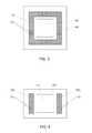
- the interposer 120 may surround the microelectronic die 102 , and may have the interconnects 172 dispersed on all sides of the interposer 120 . As shown in FIG. 4 , the interposer 120 may be two separate sections (shown as elements 120 1 and 120 2 ) on opposing sides of the microelectronic die 102 .
- FIGS. 5 and 6 illustrate an embodiment of the present description wherein an interposer 180 may be positioned on one side 108 of the microelectronic die 102 in the manner described with regard to the embodiments of FIGS. 1-4 .
- the stacked microelectronic die 170 may be attached to the interposer 180 through the plurality of interconnects 172 (shown as solder balls).
- FIGS. 7 and 8 illustrate cross-sectional views of a bumpless build-up layer—coreless substrate technology (BBUL-C) microelectronic package having an interposer integrated with the microelectronic die, in accordance with another embodiment of the present description.
- a microelectronic package 200 may include at least one microelectronic die 202 , where the microelectronic die 202 includes an active surface 204 , a back surface 206 that is substantially parallel to the microelectronic die active surface 204 , and at least two opposing sides 208 extending from the microelectronic die active surface 204 to the microelectronic die back surface 206 .
- BBUL-C bumpless build-up layer—coreless substrate technology
- the microelectronic die 202 may have an active area 210 in a central portion of the microelectronic die 202 , where integrated circuits are formed, as will be understood to those skilled in the art.
- the microelectronic die 202 may further include an interposer area 230 between the microelectronic die active area 210 and at least one microelectronic die side 208 , and may be an area where no integrated circuitry (not shown) is formed.
- the interposer area 230 may be the street area of a microelectronic wafer, as will be understood to those skilled in the art, or may be accommodated by enlarging the size of the microelectronic die 202 .
- the microelectronic die 202 may further include at least one contact land 212 on the microelectronic die active surface 204 within the microelectronic die active area 210 , wherein the microelectronic die contact lands 212 may be connected to integrated circuits (not shown) within the microelectronic die 202 .
- the microelectronic die 202 may be any appropriate integrated circuit device including but not limited to a processor or microprocessor (single or multi-core), a chipset, a graphics device, an application specific integrated circuit, or the like.
- the microelectronic die contact lands 212 may be any appropriate conductive material, including but not limited to copper, aluminum, silver, gold, or alloys thereof.
- An interposer 220 may be formed within the interposer area 230 .
- the interposer 220 may have at least one conductive via 232 extending from the microelectronic die active surface 204 to the microelectronic die back surface 206 .
- Each interposer conductive via 232 may have a contact land 234 on the microelectronic die active surface 204 and a contact land 236 on the microelectronic die back surface 206 .
- the interposer conductive vias 232 , the interposer front surface contact land 234 , and the interposer back surface contact land 236 may be fabricated by any technique know in the art, and may be made of any appropriate conductive material, including but not limited to copper, aluminum, silver, gold, or alloys thereof.
- An encapsulation material 242 may be disposed adjacent the sides 208 of the microelectronic die 202 , thereby forming a substrate 248 .
- a back surface 244 of the encapsulation material 242 may be formed to be substantially planar with the microelectronic die back surface 206 . As previously described with regard to the encapsulation material 142 of FIGS.
- the encapsulation material 242 may be any appropriate dielectric material, including, but not limited to silica-filled epoxies, such as are available from Ajinomoto Fine-Techno Co., Inc., 1-2 Suzuki-cho, Kawasaki-ku, Kawasaki-shi, 210-0801, Japan (Ajinomoto GX13, Ajinomoto GX92, and the like).
- the build-up layer 150 may be formed on the encapsulation material front surface 246 in the same manner as described for FIGS. 1 and 2 . Referring to FIG. 6 , the build-up layer 150 may be used to connect the microelectronic die contact lands 212 to the interposer front surface contact lands 234 or to connect the microelectronic die 202 to external interconnects 162 (see FIG. 5 ). These connections are shown as dashed lines 164 in FIG. 7 .
- the external interconnects 162 may be solder balls (as shown in FIG. 5 ) or pins (not shown) and may be used to connect the microelectronic package 200 to external devices (not shown).
- a stacked microelectronic die 270 may be attached to the interposer 220 through a plurality of interconnects 272 (shown as solder balls).
- the stacked microelectronic die 270 may extend over the microelectronic die back surface 206 and be attached to the interposer 220 on an opposing side of the microelectronic die 202 .
- the microelectronic die 202 is a microprocessor and the stacked microelectronic die 270 is a memory device.
- the interposer 220 may surround the microelectronic die 202 , and may have the plurality of interconnects 272 dispersed on all sides of the interposer 220 . As shown in FIG. 10 , the interposer 220 may be two separate sections (shown as elements 220 1 and 220 2 ) on opposing sides of the microelectronic die 202 .
- FIGS. 11 and 12 illustrate an embodiment of the present description wherein an interposer 280 may be formed on one side 208 of the microelectronic die 202 in the manner described with regard to the embodiments of FIGS. 7-10 .
- the stacked microelectronic die 270 may be attached to the interposer 280 through the plurality of interconnects 272 (shown as solder balls).
- the interposer of the present description may result in a high-interconnection density (e.g. greater than about 30 per square millimeter) between the microelectronic dice 102 and 202 and the stacked microelectronic dice 170 and 270 , while minimizing the impact to silicon layer design rules and processes.
- the stacked microelectronic dice 170 and 270 are shown as a single die, they may be pre-stacked dice, as will be understood to those skilled in the art.
- FIG. 13 An embodiment of a process 300 of the present description is illustrated in FIG. 13 .
- a microelectronic die may be provided.
- An interposer may be provided proximate at least one side of the microelectronic die, as defined in block 320 .
- An encapsulation material may be disposed adjacent at least one side of the microelectronic die, as defined in block 330 .
- a stacked microelectronic die may be attached to the interposer.
- any two components herein combined to achieve a particular functionality can be seen as “associated with” each other such that the desired functionality is achieved, irrespective of structures or intermediate components.
- any two components so associated can also be viewed as being “operably connected”, or “operably coupled”, to each other to achieve the desired functionality, and any two components capable of being so associated can also be viewed as being “operably couplable”, to each other to achieve the desired functionality.
- operably couplable include but are not limited to physically mateable and/or physically interacting components and/or wirelessly interactable and/or wirelessly interacting components and/or logically interacting and/or logically interactable components.
- an embodiment may mean that a particular feature, structure, or characteristic described in connection with one or more embodiments may be included in at least some embodiments, but not necessarily in all embodiments.
- the various uses of the terms “an embodiment,” “one embodiment,” “another embodiment,” or “other embodiments” in the detailed description are not necessarily all referring to the same embodiments.
Abstract
The present disclosure relates to the field of integrated circuit package design and, more particularly, to packages using a bumpless build-up layer (BBUL) designs. Embodiments of the present description relate to the field of fabricating microelectronic packages, wherein an interposer, such as a through-silicon via interposer, may be used in a bumpless build-up layer package to facilitate stacked microelectronic components.
Description
The present application is a continuation of U.S. patent application Ser. No. 12/827,323 filed Jun. 30, 2010 entitled “BUMPLESS BUILD-UP LAYER PACKAGE DESIGN WITH AN INTERPOSER”.
Embodiments of the present description generally relate to the field of microelectronic device package designs and, more particularly, to packages using a bumpless build-up layer (BBUL) designs. With shrinking microelectronic electronic device sizes, microelectronic device packages need to occupy less space, which may be achieved by stacking microelectronic components.
The subject matter of the present disclosure is particularly pointed out and distinctly claimed in the concluding portion of the specification. The foregoing and other features of the present disclosure will become more fully apparent from the following description and appended claims, taken in conjunction with the accompanying drawings. It is understood that the accompanying drawings depict only several embodiments in accordance with the present disclosure and are, therefore, not to be considered limiting of its scope. The disclosure will be described with additional specificity and detail through use of the accompanying drawings, such that the advantages of the present disclosure can be more readily ascertained, in which:
In the following detailed description, reference is made to the accompanying drawings that show, by way of illustration, specific embodiments in which the claimed subject matter may be practiced. These embodiments are described in sufficient detail to enable those skilled in the art to practice the subject matter. It is to be understood that the various embodiments, although different, are not necessarily mutually exclusive. For example, a particular feature, structure, or characteristic described herein, in connection with one embodiment, may be implemented within other embodiments without departing from the spirit and scope of the claimed subject matter. In addition, it is to be understood that the location or arrangement of individual elements within each disclosed embodiment may be modified without departing from the spirit and scope of the claimed subject matter. The following detailed description is, therefore, not to be taken in a limiting sense, and the scope of the subject matter is defined only by the appended claims, appropriately interpreted, along with the full range of equivalents to which the appended claims are entitled. In the drawings, like numerals refer to the same or similar elements or functionality throughout the several views, and that elements depicted therein are not necessarily to scale with one another, rather individual elements may be enlarged or reduced in order to more easily comprehend the elements in the context of the present description.
Embodiments of the present description relate to the field of fabricating microelectronic packages, wherein an interposer, such as a through-silicon via interposer, may be used in a bumpless build-up layer package to facilitate stacked microelectronic components.
Referring to FIG. 2 , the microelectronic die 102 may further include at least one contact land 112 on the microelectronic die active surface 104, wherein each microelectronic die contact land 112 may be connected to integrated circuits (not shown) within the microelectronic die 102. The microelectronic die 102 may be any appropriate integrated circuit device including but not limited to a processor or microprocessor (single or multi-core), a memory device, a chipset, a graphics device, an application specific integrated circuit, or the like. The microelectronic die contact lands 112 may be any appropriate conductive material, including but not limited to copper, aluminum, silver, gold, or alloys thereof.
The microelectronic package 100 may further include an interposer 120 positioned proximate at least one microelectronic die side 108, where the interposer 120 includes a front surface 124, an opposing back surface 126 that is substantially parallel to the interposer front surface 124, and at least one side 128 extending from the interposer front surface 124 to the interposer back surface 126, as shown in FIG. 2 . The interposer 120 may have at least one conductive via 132 extending therethrough from the interposer front surface 124 to the interposer back surface 126. Each interposer conductive via 132 may have a contact land 134 on the interposer front surface 124 and a contact land 136 on the interposer back surface 126. The interposer conductive vias 132, the interposer front surface contact lands 134, the interposer back surface contact lands 136 may be fabricated by any technique know in the art, and may be made of any appropriate conductive material, including but not limited to copper, aluminum, silver, gold, or alloys thereof.
In one embodiment, the interposer 120 may be a silicon-containing material, such as amorphous silicon or silicon-germanium, or a ceramic material. In another embodiment, the interposer 120 may be the same silicon material as the predominate material in the microelectronic die 102 to minimize thermal expansion mismatch, as will be understood to those skilled in the art.
The interposer 120 may be designed such that the interposer back surface 126 is substantially planar to the microelectronic die back surface 106, and may be designed such that the interposer front surface 124 is substantially planar to the microelectronic die active surface 104. An encapsulation material 142 may be disposed adjacent the microelectronic die sides 108 and the interposer sides 128, thereby forming a substrate 148. A back surface 144 of the encapsulation material 142 may be formed to be substantially planar with the interposer back surface 126 and substantially planar with the microelectronic die back surface 106. The encapsulation material 142 may be any appropriate dielectric material, including, but not limited to silica-filled epoxies, such as are available from Ajinomoto Fine-Techno Co., Inc., 1-2 Suzuki-cho, Kawasaki-ku, Kawasaki-shi, 210-0801, Japan (Ajinomoto GX13, Ajinomoto GX92, and the like).
A build-up layer 150 may be formed on the encapsulation material front surface 146. The build-up layer 150 may comprise a plurality of dielectric layers with conductive traces formed on each dielectric layer with conductive vias extending through each dielectric layer to connect the conductive traces and/or other microelectronic components on different layers. Referring to FIG. 2 , the build-up layer 150 may comprise at least one first layer conductive trace 152 connected to at least one microelectronic die contact land 112 and/or at least one interposer front surface contact land 134 through a trace-to-microelectronic die conductive via 153 and a trace-to-interposer conductive via 155, respectively, formed through the encapsulation material 142. A dielectric layer 154 may be formed adjacent at least one first layer conductive trace 152 and encapsulation material front surface 146. At least one conductive via 156 may extend through the dielectric layer 154 to connect at least one first layer conductive trace 152 to at least one second layer conductive trace 158. The build-up layer 150 may be used to connect the microelectronic die 102 to the interposer 120 or to connect the microelectronic die 102 to external interconnects 162 (shown in FIG. 1 ). These connections are shown as dashed lines 164 in FIG. 1 . The external interconnects 162 may be solder balls (as shown in FIG. 1 ) or pins (not shown) and may be used to connect the microelectronic package 100 to external devices (not shown).
It is understood that although only one dielectric layer and two conductive trace layers are shown, the build-up layer 150 may be any appropriate number of dielectric layers and conductive trace layers. The dielectric layer(s), such as the dielectric layer 154, may formed by any technique known in the art and may be formed from any appropriate dielectric material. The conductive trace layers, such as first layer conductive trace 152 and the second layer conductive trace 158, and the conductive vias 156, may be fabricated by any technique known in the art, and may be made of any appropriate conductive material, including but not limited to copper, aluminum, silver, gold, or alloys thereof.
As shown in FIG. 1 , a stacked microelectronic die 170 may be attached to the interposer 120 through a plurality of interconnects 172 (shown as solder balls). The stacked microelectronic die 170 may extend over the microelectronic die back surface 106 and be attached to the interposer 120 on an opposing side of the microelectronic die 102. The stacked microelectronic die 170 may be any appropriate integrated circuit device including but not limited to a processor or microprocessor (single or multi-core), a memory device, a chipset, a graphics device, an application specific integrated circuit, or the like. In one embodiment, the microelectronic die 102 is a microprocessor and the stacked microelectronic die 170 is a memory device.
As shown in FIG. 3 , the interposer 120 may surround the microelectronic die 102, and may have the interconnects 172 dispersed on all sides of the interposer 120. As shown in FIG. 4 , the interposer 120 may be two separate sections (shown as elements 120 1 and 120 2) on opposing sides of the microelectronic die 102.
It is understood that the stacked microelectronic die 170 need not span the microelectronic die 102, as shown in FIG. 1 . FIGS. 5 and 6 illustrate an embodiment of the present description wherein an interposer 180 may be positioned on one side 108 of the microelectronic die 102 in the manner described with regard to the embodiments of FIGS. 1-4 . Referring to FIG. 5 , the stacked microelectronic die 170 may be attached to the interposer 180 through the plurality of interconnects 172 (shown as solder balls).
Referring to FIG. 8 , the microelectronic die 202 may further include at least one contact land 212 on the microelectronic die active surface 204 within the microelectronic die active area 210, wherein the microelectronic die contact lands 212 may be connected to integrated circuits (not shown) within the microelectronic die 202. The microelectronic die 202 may be any appropriate integrated circuit device including but not limited to a processor or microprocessor (single or multi-core), a chipset, a graphics device, an application specific integrated circuit, or the like. The microelectronic die contact lands 212 may be any appropriate conductive material, including but not limited to copper, aluminum, silver, gold, or alloys thereof.
An interposer 220 may be formed within the interposer area 230. The interposer 220 may have at least one conductive via 232 extending from the microelectronic die active surface 204 to the microelectronic die back surface 206. Each interposer conductive via 232 may have a contact land 234 on the microelectronic die active surface 204 and a contact land 236 on the microelectronic die back surface 206. The interposer conductive vias 232, the interposer front surface contact land 234, and the interposer back surface contact land 236 may be fabricated by any technique know in the art, and may be made of any appropriate conductive material, including but not limited to copper, aluminum, silver, gold, or alloys thereof.
An encapsulation material 242 may be disposed adjacent the sides 208 of the microelectronic die 202, thereby forming a substrate 248. A back surface 244 of the encapsulation material 242 may be formed to be substantially planar with the microelectronic die back surface 206. As previously described with regard to the encapsulation material 142 of FIGS. 1-6 , the encapsulation material 242 may be any appropriate dielectric material, including, but not limited to silica-filled epoxies, such as are available from Ajinomoto Fine-Techno Co., Inc., 1-2 Suzuki-cho, Kawasaki-ku, Kawasaki-shi, 210-0801, Japan (Ajinomoto GX13, Ajinomoto GX92, and the like).
The build-up layer 150 may be formed on the encapsulation material front surface 246 in the same manner as described for FIGS. 1 and 2 . Referring to FIG. 6 , the build-up layer 150 may be used to connect the microelectronic die contact lands 212 to the interposer front surface contact lands 234 or to connect the microelectronic die 202 to external interconnects 162 (see FIG. 5 ). These connections are shown as dashed lines 164 in FIG. 7 . The external interconnects 162 may be solder balls (as shown in FIG. 5 ) or pins (not shown) and may be used to connect the microelectronic package 200 to external devices (not shown).
As shown in FIG. 7 , a stacked microelectronic die 270 may be attached to the interposer 220 through a plurality of interconnects 272 (shown as solder balls). The stacked microelectronic die 270 may extend over the microelectronic die back surface 206 and be attached to the interposer 220 on an opposing side of the microelectronic die 202. In one embodiment, the microelectronic die 202 is a microprocessor and the stacked microelectronic die 270 is a memory device.
As shown in FIG. 9 , the interposer 220 may surround the microelectronic die 202, and may have the plurality of interconnects 272 dispersed on all sides of the interposer 220. As shown in FIG. 10 , the interposer 220 may be two separate sections (shown as elements 220 1 and 220 2) on opposing sides of the microelectronic die 202.
It is understood that the stacked microelectronic die 270 need not span the microelectronic die 102. FIGS. 11 and 12 illustrate an embodiment of the present description wherein an interposer 280 may be formed on one side 208 of the microelectronic die 202 in the manner described with regard to the embodiments of FIGS. 7-10 . Referring to FIG. 11 , the stacked microelectronic die 270 may be attached to the interposer 280 through the plurality of interconnects 272 (shown as solder balls).
It is understood that the interposer of the present description may result in a high-interconnection density (e.g. greater than about 30 per square millimeter) between the microelectronic dice 102 and 202 and the stacked microelectronic dice 170 and 270, while minimizing the impact to silicon layer design rules and processes. Furthermore, although the stacked microelectronic dice 170 and 270 are shown as a single die, they may be pre-stacked dice, as will be understood to those skilled in the art.
An embodiment of a process 300 of the present description is illustrated in FIG. 13 . As defined in block 310, a microelectronic die may be provided. An interposer may be provided proximate at least one side of the microelectronic die, as defined in block 320. An encapsulation material may be disposed adjacent at least one side of the microelectronic die, as defined in block 330. As defined in block 340, a stacked microelectronic die may be attached to the interposer.
It is also understood that the subject matter of the present description is not necessarily limited to specific applications illustrated in FIGS. 1-13 . The subject matter may be applied to other stacked die applications. Furthermore, the subject matter may also be used in any appropriate application outside of the microelectronic device fabrication field.
The detailed description has described various embodiments of the devices and/or processes through the use of illustrations, block diagrams, flowcharts, and/or examples. Insofar as such illustrations, block diagrams, flowcharts, and/or examples contain one or more functions and/or operations, it will be understood by those skilled in the art that each function and/or operation within each illustration, block diagram, flowchart, and/or example can be implemented, individually and/or collectively, by a wide range of hardware, software, firmware, or virtually any combination thereof.
The described subject matter sometimes illustrates different components contained within, or connected with, different other components. It is understood that such illustrations are merely exemplary, and that many alternate structures can be implemented to achieve the same functionality. In a conceptual sense, any arrangement of components to achieve the same functionality is effectively “associated” such that the desired functionality is achieved. Thus, any two components herein combined to achieve a particular functionality can be seen as “associated with” each other such that the desired functionality is achieved, irrespective of structures or intermediate components. Likewise, any two components so associated can also be viewed as being “operably connected”, or “operably coupled”, to each other to achieve the desired functionality, and any two components capable of being so associated can also be viewed as being “operably couplable”, to each other to achieve the desired functionality. Specific examples of operably couplable include but are not limited to physically mateable and/or physically interacting components and/or wirelessly interactable and/or wirelessly interacting components and/or logically interacting and/or logically interactable components.
It will be understood by those skilled in the art that terms used herein, and especially in the appended claims are generally intended as “open” terms. In general, the terms “including” or “includes” should be interpreted as “including but not limited to” or “includes but is not limited to”, respectively. Additionally, the term “having” should be interpreted as “having at least”.
The use of plural and/or singular terms within the detailed description can be translated from the plural to the singular and/or from the singular to the plural as is appropriate to the context and/or the application.
It will be further understood by those skilled in the art that if an indication of the number of elements is used in a claim, the intent for the claim to be so limited will be explicitly recited in the claim, and in the absence of such recitation no such intent is present. Additionally, if a specific number of an introduced claim recitation is explicitly recited, those skilled in the art will recognize that such recitation should typically be interpreted to mean “at least” the recited number.
The use of the terms “an embodiment,” “one embodiment,” “some embodiments,” “another embodiment,” or “other embodiments” in the specification may mean that a particular feature, structure, or characteristic described in connection with one or more embodiments may be included in at least some embodiments, but not necessarily in all embodiments. The various uses of the terms “an embodiment,” “one embodiment,” “another embodiment,” or “other embodiments” in the detailed description are not necessarily all referring to the same embodiments.
While certain exemplary techniques have been described and shown herein using various methods and systems, it should be understood by those skilled in the art that various other modifications may be made, and equivalents may be substituted, without departing from claimed subject matter or spirit thereof. Additionally, many modifications may be made to adapt a particular situation to the teachings of claimed subject matter without departing from the central concept described herein. Therefore, it is intended that claimed subject matter not be limited to the particular examples disclosed, but that such claimed subject matter also may include all implementations falling within the scope of the appended claims, and equivalents thereof.
Claims (17)
1. A microelectronic package comprising:
a microelectronic die having an active surface, an opposing back surface, and at least two opposing sides extending between the microelectronic die active surface and the microelectronic die back surface, wherein the microelectronic die comprises a single structure formed of a single substrate material which includes an active area and an interposer area, wherein the active area includes in a central portion thereof further including integrated circuits formed therein and wherein the interposer area has no integrated circuits formed;
an interposer formed within the interposer area of the microelectronic die proximate the at least one microelectronic die side;
a build-up layer formed proximate the microelectronic die active surface, wherein the interposer area is in electrical communication with the microelectronic die active area through the build-up layer;
an encapsulation material adjacent the at least one microelectronic die side; and
a stacked microelectronic die attached to the interposer, wherein the encapsulation material includes a back surface that is coplanar to the microelectronic die back surface.
2. The microelectronic package of claim 1 , wherein the stacked microelectronic die substantially spans the microelectronic die.
3. The microelectronic package of claim 1 , wherein the interposer is proximate the at least two opposing microelectronic die sides.
4. The microelectronic package of claim 1 , wherein the interposer substantially surrounds the active area of the microelectronic die.
5. The microelectronic package of claim 1 , wherein the interposer includes a front surface and a back surface and wherein the encapsulation material back surface is substantially planar to the interposer back surface.
6. The microelectronic package of claim 1 , wherein the microelectronic die comprises a microprocessor, and wherein the stacked microelectronic die comprises a memory device.
7. A method of forming a microelectronic package, comprising:
forming a microelectronic die having an active surface, an opposing back surface, and at least two opposing sides extending between the microelectronic die active surface and the microelectronic die back surface, wherein the microelectronic die comprises a single structure formed of a single substrate material which includes an active area and an interposer area, wherein the active area includes in a central portion thereof further including integrated circuits formed therein and a wherein the interposer area has no integrated circuits formed therein;
forming an interposer within the interposer area of the microelectronic die proximate at least one microelectronic die side;
forming a build-up layer proximate the microelectronic die active surface, wherein the interposer area is in electrical communication with the microelectronic die active area through the build-up layer;
disposing an encapsulation material adjacent the at least one side of the microelectronic die; and
attaching a stacked microelectronic die to the interposer, wherein disposing the encapsulation material includes disposing the encapsulation material to form a back surface that is coplanar to the microelectronic die back surface.
8. The method of claim 7 , wherein attaching the stacked microelectronic die comprises attaching the stacked microelectronic die to the interposer to span an active area of the microelectronic die.
9. The method of claim 7 , wherein providing the interposer comprises providing the interposer proximate the at least two opposing microelectronic die sides.
10. The method of claim 7 , wherein providing the interposer comprises providing the interposer which substantially surrounds an active area of the microelectronic die.
11. The method of claim 7 , wherein providing the interposer comprises providing an interposer including a front surface and a back surface, and wherein disposing the encapsulation material comprises disposing the encapsulation material to form a back surface that is substantially planar to the interposer back surface.
12. The method of claim 7 , wherein the microelectronic die comprises a microprocessor and the stacked microelectronic die comprises a memory device.
13. A microelectronic package comprising:
a microelectronic die having an active surface, an opposing back surface, and at least two opposing sides extending between the microelectronic die active surface and the microelectronic die back surface, wherein the microelectronic die comprises a single structure formed of a single substrate material which includes an active area and an interposer area, wherein the active area includes in a central portion thereof further including integrated circuits formed therein and wherein the interposer area has no integrated circuits formed therein;
an interposer formed within the interposer area of the microelectronic die proximate the at least one microelectronic die side, wherein the interposer includes a front surface and a back surface;
a build-up layer formed proximate the microelectronic die active surface, wherein the interposer area is in electrical communication with the microelectronic die active area through the build-up layer;
an encapsulation material adjacent the at least one microelectronic die side, wherein the encapsulation material includes a back surface that is substantially planar to the interposer back surface and substantially planar to the microelectronic die back surface;
and a stacked microelectronic die attached to the interposer, wherein the encapsulation material includes a back surface that is coplanar to the microelectronic die back surface.
14. The microelectronic package of claim 13 , wherein the stacked microelectronic die substantially spans the microelectronic die.
15. The microelectronic package of claim 13 , wherein the interposer is proximate the at least two opposing microelectronic die sides.
16. The microelectronic package of claim 13 , wherein the interposer substantially surrounds the active area of the microelectronic die.
17. The microelectronic package of claim 13 , wherein the microelectronic die comprises a microprocessor, and wherein the stacked microelectronic die comprises a memory device.
Priority Applications (1)
| Application Number | Priority Date | Filing Date | Title |
|---|---|---|---|
| US13/972,048 US9818719B2 (en) | 2010-06-30 | 2013-08-21 | Bumpless build-up layer package design with an interposer |
Applications Claiming Priority (2)
| Application Number | Priority Date | Filing Date | Title |
|---|---|---|---|
| US12/827,323 US20120001339A1 (en) | 2010-06-30 | 2010-06-30 | Bumpless build-up layer package design with an interposer |
| US13/972,048 US9818719B2 (en) | 2010-06-30 | 2013-08-21 | Bumpless build-up layer package design with an interposer |
Related Parent Applications (1)
| Application Number | Title | Priority Date | Filing Date |
|---|---|---|---|
| US12/827,323 Continuation US20120001339A1 (en) | 2010-06-30 | 2010-06-30 | Bumpless build-up layer package design with an interposer |
Publications (2)
| Publication Number | Publication Date |
|---|---|
| US20130334696A1 US20130334696A1 (en) | 2013-12-19 |
| US9818719B2 true US9818719B2 (en) | 2017-11-14 |
Family
ID=45399101
Family Applications (2)
| Application Number | Title | Priority Date | Filing Date |
|---|---|---|---|
| US12/827,323 Abandoned US20120001339A1 (en) | 2010-06-30 | 2010-06-30 | Bumpless build-up layer package design with an interposer |
| US13/972,048 Active US9818719B2 (en) | 2010-06-30 | 2013-08-21 | Bumpless build-up layer package design with an interposer |
Family Applications Before (1)
| Application Number | Title | Priority Date | Filing Date |
|---|---|---|---|
| US12/827,323 Abandoned US20120001339A1 (en) | 2010-06-30 | 2010-06-30 | Bumpless build-up layer package design with an interposer |
Country Status (7)
| Country | Link |
|---|---|
| US (2) | US20120001339A1 (en) |
| EP (1) | EP2589076B1 (en) |
| KR (1) | KR101451495B1 (en) |
| CN (1) | CN102934223B (en) |
| SG (1) | SG185077A1 (en) |
| TW (1) | TWI632651B (en) |
| WO (1) | WO2012003280A2 (en) |
Families Citing this family (48)
| Publication number | Priority date | Publication date | Assignee | Title |
|---|---|---|---|---|
| US8742561B2 (en) | 2009-12-29 | 2014-06-03 | Intel Corporation | Recessed and embedded die coreless package |
| US8901724B2 (en) * | 2009-12-29 | 2014-12-02 | Intel Corporation | Semiconductor package with embedded die and its methods of fabrication |
| US8535989B2 (en) | 2010-04-02 | 2013-09-17 | Intel Corporation | Embedded semiconductive chips in reconstituted wafers, and systems containing same |
| US8319318B2 (en) | 2010-04-06 | 2012-11-27 | Intel Corporation | Forming metal filled die back-side film for electromagnetic interference shielding with coreless packages |
| US8618652B2 (en) | 2010-04-16 | 2013-12-31 | Intel Corporation | Forming functionalized carrier structures with coreless packages |
| US9847308B2 (en) | 2010-04-28 | 2017-12-19 | Intel Corporation | Magnetic intermetallic compound interconnect |
| US8939347B2 (en) | 2010-04-28 | 2015-01-27 | Intel Corporation | Magnetic intermetallic compound interconnect |
| US8434668B2 (en) | 2010-05-12 | 2013-05-07 | Intel Corporation | Magnetic attachment structure |
| US8313958B2 (en) | 2010-05-12 | 2012-11-20 | Intel Corporation | Magnetic microelectronic device attachment |
| US8609532B2 (en) | 2010-05-26 | 2013-12-17 | Intel Corporation | Magnetically sintered conductive via |
| US20120001339A1 (en) | 2010-06-30 | 2012-01-05 | Pramod Malatkar | Bumpless build-up layer package design with an interposer |
| US8372666B2 (en) | 2010-07-06 | 2013-02-12 | Intel Corporation | Misalignment correction for embedded microelectronic die applications |
| US8754516B2 (en) | 2010-08-26 | 2014-06-17 | Intel Corporation | Bumpless build-up layer package with pre-stacked microelectronic devices |
| US8304913B2 (en) | 2010-09-24 | 2012-11-06 | Intel Corporation | Methods of forming fully embedded bumpless build-up layer packages and structures formed thereby |
| US8937382B2 (en) | 2011-06-27 | 2015-01-20 | Intel Corporation | Secondary device integration into coreless microelectronic device packages |
| US8848380B2 (en) | 2011-06-30 | 2014-09-30 | Intel Corporation | Bumpless build-up layer package warpage reduction |
| US9679863B2 (en) * | 2011-09-23 | 2017-06-13 | STATS ChipPAC Pte. Ltd. | Semiconductor device and method of forming interconnect substrate for FO-WLCSP |
| US9287249B2 (en) * | 2012-04-11 | 2016-03-15 | Panasonic Intellectual Property Management Co., Ltd. | Semiconductor device |
| WO2013172814A1 (en) | 2012-05-14 | 2013-11-21 | Intel Corporation | Microelectronic package utilizing multiple bumpless build-up structures and through-silicon vias |
| CN104321864B (en) * | 2012-06-08 | 2017-06-20 | 英特尔公司 | Microelectronics Packaging with the non-coplanar, microelectronic component of encapsulating and solderless buildup layer |
| KR101364088B1 (en) | 2012-09-12 | 2014-02-20 | 전자부품연구원 | Interposer, and method for manufacturing the same |
| TWI488270B (en) * | 2012-09-26 | 2015-06-11 | 矽品精密工業股份有限公司 | Semiconductor package and method of forming the same |
| US20140091440A1 (en) * | 2012-09-29 | 2014-04-03 | Vijay K. Nair | System in package with embedded rf die in coreless substrate |
| US9620413B2 (en) | 2012-10-02 | 2017-04-11 | STATS ChipPAC Pte. Ltd. | Semiconductor device and method of using a standardized carrier in semiconductor packaging |
| US9496195B2 (en) | 2012-10-02 | 2016-11-15 | STATS ChipPAC Pte. Ltd. | Semiconductor device and method of depositing encapsulant along sides and surface edge of semiconductor die in embedded WLCSP |
| US9704824B2 (en) | 2013-01-03 | 2017-07-11 | STATS ChipPAC Pte. Ltd. | Semiconductor device and method of forming embedded wafer level chip scale packages |
| US9721862B2 (en) | 2013-01-03 | 2017-08-01 | STATS ChipPAC Pte. Ltd. | Semiconductor device and method of using a standardized carrier to form embedded wafer level chip scale packages |
| US9087765B2 (en) | 2013-03-15 | 2015-07-21 | Qualcomm Incorporated | System-in-package with interposer pitch adapter |
| US8772913B1 (en) | 2013-04-04 | 2014-07-08 | Freescale Semiconductor, Inc. | Stiffened semiconductor die package |
| US8669140B1 (en) | 2013-04-04 | 2014-03-11 | Freescale Semiconductor, Inc. | Method of forming stacked die package using redistributed chip packaging |
| KR101488608B1 (en) * | 2013-07-19 | 2015-02-02 | 앰코 테크놀로지 코리아 주식회사 | Semiconductor device and manufacturing method thereof |
| US9263370B2 (en) * | 2013-09-27 | 2016-02-16 | Qualcomm Mems Technologies, Inc. | Semiconductor device with via bar |
| US10170409B2 (en) | 2013-12-23 | 2019-01-01 | Intel Corporation | Package on package architecture and method for making |
| US20150262902A1 (en) | 2014-03-12 | 2015-09-17 | Invensas Corporation | Integrated circuits protected by substrates with cavities, and methods of manufacture |
| US9355997B2 (en) | 2014-03-12 | 2016-05-31 | Invensas Corporation | Integrated circuit assemblies with reinforcement frames, and methods of manufacture |
| US9165793B1 (en) | 2014-05-02 | 2015-10-20 | Invensas Corporation | Making electrical components in handle wafers of integrated circuit packages |
| US9741649B2 (en) | 2014-06-04 | 2017-08-22 | Invensas Corporation | Integrated interposer solutions for 2D and 3D IC packaging |
| US9252127B1 (en) | 2014-07-10 | 2016-02-02 | Invensas Corporation | Microelectronic assemblies with integrated circuits and interposers with cavities, and methods of manufacture |
| CN106030795A (en) | 2014-12-16 | 2016-10-12 | 英特尔公司 | Electronic assembly that includes stacked electronic devices |
| KR20160122022A (en) * | 2015-04-13 | 2016-10-21 | 에스케이하이닉스 주식회사 | Semiconductor package with interposer and method of manufacturing the same |
| US9478504B1 (en) | 2015-06-19 | 2016-10-25 | Invensas Corporation | Microelectronic assemblies with cavities, and methods of fabrication |
| US9741620B2 (en) * | 2015-06-24 | 2017-08-22 | Invensas Corporation | Structures and methods for reliable packages |
| US9524959B1 (en) * | 2015-11-04 | 2016-12-20 | Taiwan Semiconductor Manufacturing Company, Ltd. | System on integrated chips and methods of forming same |
| WO2018063321A1 (en) * | 2016-09-30 | 2018-04-05 | Intel Corporation | Embedded die on interposer packages |
| US10515929B2 (en) * | 2018-04-09 | 2019-12-24 | International Business Machines Corporation | Carrier and integrated memory |
| US10431563B1 (en) | 2018-04-09 | 2019-10-01 | International Business Machines Corporation | Carrier and integrated memory |
| US11450615B2 (en) * | 2020-06-12 | 2022-09-20 | Taiwan Semiconductor Manufacturing Company, Ltd. | Package structure and method of fabricating the same |
| US20230354525A1 (en) * | 2021-05-06 | 2023-11-02 | Innoscience (Suzhou) Technology Co., Ltd. | Nitride-based semiconductor module and method for manufacturing the same |
Citations (79)
| Publication number | Priority date | Publication date | Assignee | Title |
|---|---|---|---|---|
| US5353498A (en) | 1993-02-08 | 1994-10-11 | General Electric Company | Method for fabricating an integrated circuit module |
| US5527741A (en) | 1994-10-11 | 1996-06-18 | Martin Marietta Corporation | Fabrication and structures of circuit modules with flexible interconnect layers |
| US5790384A (en) | 1997-06-26 | 1998-08-04 | International Business Machines Corporation | Bare die multiple dies for direct attach |
| US5841193A (en) | 1996-05-20 | 1998-11-24 | Epic Technologies, Inc. | Single chip modules, repairable multichip modules, and methods of fabrication thereof |
| US5977640A (en) | 1998-06-26 | 1999-11-02 | International Business Machines Corporation | Highly integrated chip-on-chip packaging |
| US6154366A (en) | 1999-11-23 | 2000-11-28 | Intel Corporation | Structures and processes for fabricating moisture resistant chip-on-flex packages |
| US6232152B1 (en) | 1994-05-19 | 2001-05-15 | Tessera, Inc. | Method of manufacturing a plurality of semiconductor packages and the resulting semiconductor package structures |
| US6239482B1 (en) | 1999-06-21 | 2001-05-29 | General Electric Company | Integrated circuit package including window frame |
| US6242282B1 (en) | 1999-10-04 | 2001-06-05 | General Electric Company | Circuit chip package and fabrication method |
| US6271469B1 (en) | 1999-11-12 | 2001-08-07 | Intel Corporation | Direct build-up layer on an encapsulated die package |
| US6306680B1 (en) | 1999-02-22 | 2001-10-23 | General Electric Company | Power overlay chip scale packages for discrete power devices |
| US20020031867A1 (en) | 2000-09-14 | 2002-03-14 | Michio Horiuchi | Semiconductor device and process of production of same |
| US6396148B1 (en) | 2000-02-10 | 2002-05-28 | Epic Technologies, Inc. | Electroless metal connection structures and methods |
| US6423570B1 (en) | 2000-10-18 | 2002-07-23 | Intel Corporation | Method to protect an encapsulated die package during back grinding with a solder metallization layer and devices formed thereby |
| US6426545B1 (en) | 2000-02-10 | 2002-07-30 | Epic Technologies, Inc. | Integrated circuit structures and methods employing a low modulus high elongation photodielectric |
| US6469395B1 (en) | 1999-11-25 | 2002-10-22 | Mitsubishi Denki Kabushiki Kaisha | Semiconductor device |
| US6489185B1 (en) | 2000-09-13 | 2002-12-03 | Intel Corporation | Protective film for the fabrication of direct build-up layers on an encapsulated die package |
| US6555908B1 (en) | 2000-02-10 | 2003-04-29 | Epic Technologies, Inc. | Compliant, solderable input/output bump structures |
| US6555906B2 (en) | 2000-12-15 | 2003-04-29 | Intel Corporation | Microelectronic package having a bumpless laminated interconnection layer |
| US6580611B1 (en) | 2001-12-21 | 2003-06-17 | Intel Corporation | Dual-sided heat removal system |
| US6586276B2 (en) | 2001-07-11 | 2003-07-01 | Intel Corporation | Method for fabricating a microelectronic device using wafer-level adhesion layer deposition |
| US6586822B1 (en) | 2000-09-08 | 2003-07-01 | Intel Corporation | Integrated core microelectronic package |
| US6586836B1 (en) | 2000-03-01 | 2003-07-01 | Intel Corporation | Process for forming microelectronic packages and intermediate structures formed therewith |
| US20030127737A1 (en) | 2002-01-10 | 2003-07-10 | Norio Takahashi | Semiconductor device |
| US6617682B1 (en) | 2000-09-28 | 2003-09-09 | Intel Corporation | Structure for reducing die corner and edge stresses in microelectronic packages |
| US6703400B2 (en) | 2001-02-23 | 2004-03-09 | Schering Corporation | Methods for treating multidrug resistance |
| US6706553B2 (en) | 2001-03-26 | 2004-03-16 | Intel Corporation | Dispensing process for fabrication of microelectronic packages |
| US6709898B1 (en) | 2000-10-04 | 2004-03-23 | Intel Corporation | Die-in-heat spreader microelectronic package |
| US6713859B1 (en) | 2000-09-13 | 2004-03-30 | Intel Corporation | Direct build-up layer on an encapsulated die package having a moisture barrier structure |
| US6734534B1 (en) | 2000-08-16 | 2004-05-11 | Intel Corporation | Microelectronic substrate with integrated devices |
| US20050003619A1 (en) | 2003-07-04 | 2005-01-06 | Kabushiki Kaisha Toshiba | Nonvolatile semiconductor memory and manufacturing method for the same |
| US6841413B2 (en) | 2002-01-07 | 2005-01-11 | Intel Corporation | Thinned die integrated circuit package |
| US6888240B2 (en) | 2001-04-30 | 2005-05-03 | Intel Corporation | High performance, low cost microelectronic circuit package with interposer |
| US6894399B2 (en) | 2001-04-30 | 2005-05-17 | Intel Corporation | Microelectronic device having signal distribution functionality on an interfacial layer thereof |
| US20060033199A1 (en) | 2004-08-11 | 2006-02-16 | Sony Corporation | Electronic circuit device |
| KR20060028001A (en) | 2004-09-24 | 2006-03-29 | 주식회사 하이닉스반도체 | Method for fabricating semiconductor device |
| US7071024B2 (en) | 2001-05-21 | 2006-07-04 | Intel Corporation | Method for packaging a microelectronic device using on-die bond pad expansion |
| US7078788B2 (en) | 2000-08-16 | 2006-07-18 | Intel Corporation | Microelectronic substrates with integrated devices |
| US20060175695A1 (en) | 2005-02-10 | 2006-08-10 | Stats Chippac Ltd. | Integrated circuit package system using interposer |
| US7109055B2 (en) | 2005-01-20 | 2006-09-19 | Freescale Semiconductor, Inc. | Methods and apparatus having wafer level chip scale package for sensing elements |
| US7160755B2 (en) | 2005-04-18 | 2007-01-09 | Freescale Semiconductor, Inc. | Method of forming a substrateless semiconductor package |
| US7183658B2 (en) | 2001-09-05 | 2007-02-27 | Intel Corporation | Low cost microelectronic circuit package |
| US7215033B2 (en) * | 2003-11-19 | 2007-05-08 | Samsung Electronics Co., Ltd. | Wafer level stack structure for system-in-package and method thereof |
| US20070155048A1 (en) * | 2005-12-29 | 2007-07-05 | Micron Technology, Inc. | Methods for packaging microelectronic devices and microelectronic devices formed using such methods |
| US20080029872A1 (en) | 2006-08-07 | 2008-02-07 | Phoenix Precision Technology Corporation | Plate structure having chip embedded therein and the manufacturing method of the same |
| US20080054448A1 (en) | 2006-09-01 | 2008-03-06 | Daoqiang Lu | Dual heat spreader panel assembly method for bumpless die-attach packages, packages containing same, and systems containing same |
| US20080106934A1 (en) | 2006-11-03 | 2008-05-08 | Samsung Electronics Co., Ltd | Memory device and method of operating and fabricating the same |
| US20080128916A1 (en) | 2006-12-04 | 2008-06-05 | Nec Electronics Corporation | Semiconductor device including microstrip line and coplanar line |
| US7425464B2 (en) | 2006-03-10 | 2008-09-16 | Freescale Semiconductor, Inc. | Semiconductor device packaging |
| US7442581B2 (en) | 2004-12-10 | 2008-10-28 | Freescale Semiconductor, Inc. | Flexible carrier and release method for high volume electronic package fabrication |
| US20080315377A1 (en) | 2007-06-25 | 2008-12-25 | Epic Technologies, Inc. | Packaged electronic modules and fabrication methods thereof implementing a cell phone or other electronic system |
| US7476563B2 (en) | 2006-11-17 | 2009-01-13 | Freescale Semiconductor, Inc. | Method of packaging a device using a dielectric layer |
| US20090072382A1 (en) | 2007-09-18 | 2009-03-19 | Guzek John S | Microelectronic package and method of forming same |
| US20090079063A1 (en) | 2007-09-26 | 2009-03-26 | Chrysler Gregory M | Microelectronic package and method of cooling an interconnect feature in same |
| US20090079064A1 (en) | 2007-09-25 | 2009-03-26 | Jiamiao Tang | Methods of forming a thin tim coreless high density bump-less package and structures formed thereby |
| US20090212416A1 (en) | 2008-02-22 | 2009-08-27 | Skeete Oswald L | Integrated circuit package and method of manufacturing same |
| US7588951B2 (en) | 2006-11-17 | 2009-09-15 | Freescale Semiconductor, Inc. | Method of packaging a semiconductor device and a prefabricated connector |
| US7595226B2 (en) | 2007-08-29 | 2009-09-29 | Freescale Semiconductor, Inc. | Method of packaging an integrated circuit die |
| US20090294942A1 (en) | 2008-06-03 | 2009-12-03 | Palmer Eric C | Package on package using a bump-less build up layer (bbul) package |
| US7632715B2 (en) | 2007-01-05 | 2009-12-15 | Freescale Semiconductor, Inc. | Method of packaging semiconductor devices |
| US7648858B2 (en) | 2007-06-19 | 2010-01-19 | Freescale Semiconductor, Inc. | Methods and apparatus for EMI shielding in multi-chip modules |
| US7651889B2 (en) | 2007-09-13 | 2010-01-26 | Freescale Semiconductor, Inc. | Electromagnetic shield formation for integrated circuit die package |
| US7659143B2 (en) | 2006-09-29 | 2010-02-09 | Intel Corporation | Dual-chip integrated heat spreader assembly, packages containing same, and systems containing same |
| US20100133704A1 (en) * | 2008-12-01 | 2010-06-03 | Stats Chippac, Ltd. | Semiconductor Device and Method of Forming an Interposer Package with Through Silicon Vias |
| US20100163952A1 (en) | 2008-12-31 | 2010-07-01 | Chia-Hong Jan | Flash Cell with Integrated High-K Dielectric and Metal-Based Control Gate |
| US20110068444A1 (en) * | 2009-09-23 | 2011-03-24 | Stats Chippac, Ltd. | Semiconductor Device and Method of Forming Open Cavity in TSV Interposer to Contain Semiconductor Die in WLCSMP |
| US20110101491A1 (en) | 2007-09-25 | 2011-05-05 | Oswald Skeete | Integrated circuit packages including high density bump-less build up layers and a lesser density core or coreless substrate |
| US20110108999A1 (en) | 2009-11-06 | 2011-05-12 | Nalla Ravi K | Microelectronic package and method of manufacturing same |
| US20110156231A1 (en) | 2009-12-29 | 2011-06-30 | Intel Corporation | Recessed and embedded die coreless package |
| US20110215464A1 (en) | 2009-12-29 | 2011-09-08 | Intel Corporation | Semiconductor package with embedded die and its methods of fabrication |
| US20110228464A1 (en) | 2010-03-17 | 2011-09-22 | Guzek John S | System-in-package using embedded-die coreless substrates, and processes of forming same |
| US20110254124A1 (en) | 2010-04-16 | 2011-10-20 | Nalla Ravi K | Forming functionalized carrier structures with coreless packages |
| WO2012003280A2 (en) | 2010-06-30 | 2012-01-05 | Intel Corporation | Bumpless build-up layer package design with an interposer |
| US20120049382A1 (en) | 2010-08-26 | 2012-03-01 | Pramod Malatkar | Bumpless build-up layer package with pre-stacked microelectronic devices |
| US8313958B2 (en) | 2010-05-12 | 2012-11-20 | Intel Corporation | Magnetic microelectronic device attachment |
| US8319318B2 (en) | 2010-04-06 | 2012-11-27 | Intel Corporation | Forming metal filled die back-side film for electromagnetic interference shielding with coreless packages |
| US8372666B2 (en) | 2010-07-06 | 2013-02-12 | Intel Corporation | Misalignment correction for embedded microelectronic die applications |
| US8431438B2 (en) | 2010-04-06 | 2013-04-30 | Intel Corporation | Forming in-situ micro-feature structures with coreless packages |
| US8535989B2 (en) | 2010-04-02 | 2013-09-17 | Intel Corporation | Embedded semiconductive chips in reconstituted wafers, and systems containing same |
-
2010
- 2010-06-30 US US12/827,323 patent/US20120001339A1/en not_active Abandoned
-
2011
- 2011-06-30 TW TW100123125A patent/TWI632651B/en not_active IP Right Cessation
- 2011-06-30 WO PCT/US2011/042534 patent/WO2012003280A2/en active Application Filing
- 2011-06-30 CN CN201180027611.XA patent/CN102934223B/en not_active Expired - Fee Related
- 2011-06-30 KR KR1020127031945A patent/KR101451495B1/en active IP Right Grant
- 2011-06-30 SG SG2012079844A patent/SG185077A1/en unknown
- 2011-06-30 EP EP11801390.3A patent/EP2589076B1/en active Active
-
2013
- 2013-08-21 US US13/972,048 patent/US9818719B2/en active Active
Patent Citations (100)
| Publication number | Priority date | Publication date | Assignee | Title |
|---|---|---|---|---|
| US5497033A (en) | 1993-02-08 | 1996-03-05 | Martin Marietta Corporation | Embedded substrate for integrated circuit modules |
| US5353498A (en) | 1993-02-08 | 1994-10-11 | General Electric Company | Method for fabricating an integrated circuit module |
| US6232152B1 (en) | 1994-05-19 | 2001-05-15 | Tessera, Inc. | Method of manufacturing a plurality of semiconductor packages and the resulting semiconductor package structures |
| US5527741A (en) | 1994-10-11 | 1996-06-18 | Martin Marietta Corporation | Fabrication and structures of circuit modules with flexible interconnect layers |
| US5841193A (en) | 1996-05-20 | 1998-11-24 | Epic Technologies, Inc. | Single chip modules, repairable multichip modules, and methods of fabrication thereof |
| US6159767A (en) | 1996-05-20 | 2000-12-12 | Epic Technologies, Inc. | Single chip modules, repairable multichip modules, and methods of fabrication thereof |
| US5790384A (en) | 1997-06-26 | 1998-08-04 | International Business Machines Corporation | Bare die multiple dies for direct attach |
| US5977640A (en) | 1998-06-26 | 1999-11-02 | International Business Machines Corporation | Highly integrated chip-on-chip packaging |
| US6306680B1 (en) | 1999-02-22 | 2001-10-23 | General Electric Company | Power overlay chip scale packages for discrete power devices |
| US6239482B1 (en) | 1999-06-21 | 2001-05-29 | General Electric Company | Integrated circuit package including window frame |
| US6242282B1 (en) | 1999-10-04 | 2001-06-05 | General Electric Company | Circuit chip package and fabrication method |
| US6396153B2 (en) | 1999-10-04 | 2002-05-28 | General Electric Company | Circuit chip package and fabrication method |
| US6271469B1 (en) | 1999-11-12 | 2001-08-07 | Intel Corporation | Direct build-up layer on an encapsulated die package |
| US6154366A (en) | 1999-11-23 | 2000-11-28 | Intel Corporation | Structures and processes for fabricating moisture resistant chip-on-flex packages |
| US6469395B1 (en) | 1999-11-25 | 2002-10-22 | Mitsubishi Denki Kabushiki Kaisha | Semiconductor device |
| US6555908B1 (en) | 2000-02-10 | 2003-04-29 | Epic Technologies, Inc. | Compliant, solderable input/output bump structures |
| US6396148B1 (en) | 2000-02-10 | 2002-05-28 | Epic Technologies, Inc. | Electroless metal connection structures and methods |
| US7112467B2 (en) | 2000-02-10 | 2006-09-26 | Epic Technologies, Inc. | Structure and method for temporarily holding integrated circuit chips in accurate alignment |
| US6426545B1 (en) | 2000-02-10 | 2002-07-30 | Epic Technologies, Inc. | Integrated circuit structures and methods employing a low modulus high elongation photodielectric |
| US6818544B2 (en) | 2000-02-10 | 2004-11-16 | Epic Technologies, Inc. | Compliant, solderable input/output bump structures |
| US7189596B1 (en) | 2000-03-01 | 2007-03-13 | Intel Corporation | Process for forming a direct build-up layer on an encapsulated die packages utilizing intermediate structures |
| US6586836B1 (en) | 2000-03-01 | 2003-07-01 | Intel Corporation | Process for forming microelectronic packages and intermediate structures formed therewith |
| US6734534B1 (en) | 2000-08-16 | 2004-05-11 | Intel Corporation | Microelectronic substrate with integrated devices |
| US7078788B2 (en) | 2000-08-16 | 2006-07-18 | Intel Corporation | Microelectronic substrates with integrated devices |
| US6586822B1 (en) | 2000-09-08 | 2003-07-01 | Intel Corporation | Integrated core microelectronic package |
| US6825063B2 (en) | 2000-09-08 | 2004-11-30 | Intel Corporation | Integrated core microelectronic package |
| US7416918B2 (en) | 2000-09-13 | 2008-08-26 | Intel Corporation | Direct build-up layer on an encapsulated die package having a moisture barrier structure |
| US6713859B1 (en) | 2000-09-13 | 2004-03-30 | Intel Corporation | Direct build-up layer on an encapsulated die package having a moisture barrier structure |
| US6489185B1 (en) | 2000-09-13 | 2002-12-03 | Intel Corporation | Protective film for the fabrication of direct build-up layers on an encapsulated die package |
| US20020031867A1 (en) | 2000-09-14 | 2002-03-14 | Michio Horiuchi | Semiconductor device and process of production of same |
| EP1189273A2 (en) | 2000-09-14 | 2002-03-20 | Shinko Electric Industries Co. Ltd. | Semiconductor device and production process |
| US6617682B1 (en) | 2000-09-28 | 2003-09-09 | Intel Corporation | Structure for reducing die corner and edge stresses in microelectronic packages |
| US6794223B2 (en) | 2000-09-28 | 2004-09-21 | Intel Corporation | Structure and process for reducing die corner and edge stresses in microelectronic packages |
| US6709898B1 (en) | 2000-10-04 | 2004-03-23 | Intel Corporation | Die-in-heat spreader microelectronic package |
| US6902950B2 (en) | 2000-10-18 | 2005-06-07 | Intel Corporation | Method to protect an encapsulated die package during back grinding with a solder metallization layer and devices formed thereby |
| US6423570B1 (en) | 2000-10-18 | 2002-07-23 | Intel Corporation | Method to protect an encapsulated die package during back grinding with a solder metallization layer and devices formed thereby |
| US6964889B2 (en) | 2000-10-18 | 2005-11-15 | Intel Corporation | Method to protect an encapsulated die package during back grinding with a solder metallization layer and devices formed thereby |
| US7067356B2 (en) | 2000-12-15 | 2006-06-27 | Intel Corporation | Method of fabricating microelectronic package having a bumpless laminated interconnection layer |
| US6555906B2 (en) | 2000-12-15 | 2003-04-29 | Intel Corporation | Microelectronic package having a bumpless laminated interconnection layer |
| US6703400B2 (en) | 2001-02-23 | 2004-03-09 | Schering Corporation | Methods for treating multidrug resistance |
| US6706553B2 (en) | 2001-03-26 | 2004-03-16 | Intel Corporation | Dispensing process for fabrication of microelectronic packages |
| US6894399B2 (en) | 2001-04-30 | 2005-05-17 | Intel Corporation | Microelectronic device having signal distribution functionality on an interfacial layer thereof |
| US6888240B2 (en) | 2001-04-30 | 2005-05-03 | Intel Corporation | High performance, low cost microelectronic circuit package with interposer |
| US7071024B2 (en) | 2001-05-21 | 2006-07-04 | Intel Corporation | Method for packaging a microelectronic device using on-die bond pad expansion |
| US6586276B2 (en) | 2001-07-11 | 2003-07-01 | Intel Corporation | Method for fabricating a microelectronic device using wafer-level adhesion layer deposition |
| US7183658B2 (en) | 2001-09-05 | 2007-02-27 | Intel Corporation | Low cost microelectronic circuit package |
| US6580611B1 (en) | 2001-12-21 | 2003-06-17 | Intel Corporation | Dual-sided heat removal system |
| US6841413B2 (en) | 2002-01-07 | 2005-01-11 | Intel Corporation | Thinned die integrated circuit package |
| US7420273B2 (en) | 2002-01-07 | 2008-09-02 | Intel Corporation | Thinned die integrated circuit package |
| US20030127737A1 (en) | 2002-01-10 | 2003-07-10 | Norio Takahashi | Semiconductor device |
| US20050003619A1 (en) | 2003-07-04 | 2005-01-06 | Kabushiki Kaisha Toshiba | Nonvolatile semiconductor memory and manufacturing method for the same |
| US7215033B2 (en) * | 2003-11-19 | 2007-05-08 | Samsung Electronics Co., Ltd. | Wafer level stack structure for system-in-package and method thereof |
| US20060033199A1 (en) | 2004-08-11 | 2006-02-16 | Sony Corporation | Electronic circuit device |
| KR20060028001A (en) | 2004-09-24 | 2006-03-29 | 주식회사 하이닉스반도체 | Method for fabricating semiconductor device |
| US7442581B2 (en) | 2004-12-10 | 2008-10-28 | Freescale Semiconductor, Inc. | Flexible carrier and release method for high volume electronic package fabrication |
| US7109055B2 (en) | 2005-01-20 | 2006-09-19 | Freescale Semiconductor, Inc. | Methods and apparatus having wafer level chip scale package for sensing elements |
| US20060175695A1 (en) | 2005-02-10 | 2006-08-10 | Stats Chippac Ltd. | Integrated circuit package system using interposer |
| US7160755B2 (en) | 2005-04-18 | 2007-01-09 | Freescale Semiconductor, Inc. | Method of forming a substrateless semiconductor package |
| US20070155048A1 (en) * | 2005-12-29 | 2007-07-05 | Micron Technology, Inc. | Methods for packaging microelectronic devices and microelectronic devices formed using such methods |
| US7425464B2 (en) | 2006-03-10 | 2008-09-16 | Freescale Semiconductor, Inc. | Semiconductor device packaging |
| US20080029872A1 (en) | 2006-08-07 | 2008-02-07 | Phoenix Precision Technology Corporation | Plate structure having chip embedded therein and the manufacturing method of the same |
| US20080054448A1 (en) | 2006-09-01 | 2008-03-06 | Daoqiang Lu | Dual heat spreader panel assembly method for bumpless die-attach packages, packages containing same, and systems containing same |
| US7659143B2 (en) | 2006-09-29 | 2010-02-09 | Intel Corporation | Dual-chip integrated heat spreader assembly, packages containing same, and systems containing same |
| US20080106934A1 (en) | 2006-11-03 | 2008-05-08 | Samsung Electronics Co., Ltd | Memory device and method of operating and fabricating the same |
| US7655502B2 (en) | 2006-11-17 | 2010-02-02 | Freescale Semiconductor, Inc. | Method of packaging a semiconductor device and a prefabricated connector |
| US7476563B2 (en) | 2006-11-17 | 2009-01-13 | Freescale Semiconductor, Inc. | Method of packaging a device using a dielectric layer |
| US7588951B2 (en) | 2006-11-17 | 2009-09-15 | Freescale Semiconductor, Inc. | Method of packaging a semiconductor device and a prefabricated connector |
| CN101197343A (en) | 2006-12-04 | 2008-06-11 | 恩益禧电子股份有限公司 | Semiconductor device including microstrip line and coplanar line |
| US20080128916A1 (en) | 2006-12-04 | 2008-06-05 | Nec Electronics Corporation | Semiconductor device including microstrip line and coplanar line |
| US7632715B2 (en) | 2007-01-05 | 2009-12-15 | Freescale Semiconductor, Inc. | Method of packaging semiconductor devices |
| US7648858B2 (en) | 2007-06-19 | 2010-01-19 | Freescale Semiconductor, Inc. | Methods and apparatus for EMI shielding in multi-chip modules |
| US20080315377A1 (en) | 2007-06-25 | 2008-12-25 | Epic Technologies, Inc. | Packaged electronic modules and fabrication methods thereof implementing a cell phone or other electronic system |
| US20080315391A1 (en) | 2007-06-25 | 2008-12-25 | Epic Technologies, Inc. | Integrated structures and methods of fabrication thereof with fan-out metallization on a chips-first chip layer |
| US20100047970A1 (en) | 2007-06-25 | 2010-02-25 | Epic Technologies, Inc. | Integrated conductive structures and fabrication methods thereof facilitating implementing a cell phone or other electronic system |
| US20100044855A1 (en) | 2007-06-25 | 2010-02-25 | Epic Technologies, Inc. | Integrated thermal structures and fabrication methods thereof facilitating implementing a cell phone or other electronic system |
| US7619901B2 (en) | 2007-06-25 | 2009-11-17 | Epic Technologies, Inc. | Integrated structures and fabrication methods thereof implementing a cell phone or other electronic system |
| US7595226B2 (en) | 2007-08-29 | 2009-09-29 | Freescale Semiconductor, Inc. | Method of packaging an integrated circuit die |
| US7651889B2 (en) | 2007-09-13 | 2010-01-26 | Freescale Semiconductor, Inc. | Electromagnetic shield formation for integrated circuit die package |
| US20090072382A1 (en) | 2007-09-18 | 2009-03-19 | Guzek John S | Microelectronic package and method of forming same |
| US20090079064A1 (en) | 2007-09-25 | 2009-03-26 | Jiamiao Tang | Methods of forming a thin tim coreless high density bump-less package and structures formed thereby |
| US20110101491A1 (en) | 2007-09-25 | 2011-05-05 | Oswald Skeete | Integrated circuit packages including high density bump-less build up layers and a lesser density core or coreless substrate |
| US20090079063A1 (en) | 2007-09-26 | 2009-03-26 | Chrysler Gregory M | Microelectronic package and method of cooling an interconnect feature in same |
| US20090212416A1 (en) | 2008-02-22 | 2009-08-27 | Skeete Oswald L | Integrated circuit package and method of manufacturing same |
| US20090294942A1 (en) | 2008-06-03 | 2009-12-03 | Palmer Eric C | Package on package using a bump-less build up layer (bbul) package |
| US20100133704A1 (en) * | 2008-12-01 | 2010-06-03 | Stats Chippac, Ltd. | Semiconductor Device and Method of Forming an Interposer Package with Through Silicon Vias |
| US20100163952A1 (en) | 2008-12-31 | 2010-07-01 | Chia-Hong Jan | Flash Cell with Integrated High-K Dielectric and Metal-Based Control Gate |
| WO2010078189A2 (en) | 2008-12-31 | 2010-07-08 | Intel Corporation | Flash cell with integrated high-k dielectric and metal-based control gate |
| US20110068444A1 (en) * | 2009-09-23 | 2011-03-24 | Stats Chippac, Ltd. | Semiconductor Device and Method of Forming Open Cavity in TSV Interposer to Contain Semiconductor Die in WLCSMP |
| US20110108999A1 (en) | 2009-11-06 | 2011-05-12 | Nalla Ravi K | Microelectronic package and method of manufacturing same |
| US20110156231A1 (en) | 2009-12-29 | 2011-06-30 | Intel Corporation | Recessed and embedded die coreless package |
| US20110215464A1 (en) | 2009-12-29 | 2011-09-08 | Intel Corporation | Semiconductor package with embedded die and its methods of fabrication |
| US20110228464A1 (en) | 2010-03-17 | 2011-09-22 | Guzek John S | System-in-package using embedded-die coreless substrates, and processes of forming same |
| US8535989B2 (en) | 2010-04-02 | 2013-09-17 | Intel Corporation | Embedded semiconductive chips in reconstituted wafers, and systems containing same |
| US8319318B2 (en) | 2010-04-06 | 2012-11-27 | Intel Corporation | Forming metal filled die back-side film for electromagnetic interference shielding with coreless packages |
| US8431438B2 (en) | 2010-04-06 | 2013-04-30 | Intel Corporation | Forming in-situ micro-feature structures with coreless packages |
| US20110254124A1 (en) | 2010-04-16 | 2011-10-20 | Nalla Ravi K | Forming functionalized carrier structures with coreless packages |
| US8313958B2 (en) | 2010-05-12 | 2012-11-20 | Intel Corporation | Magnetic microelectronic device attachment |
| WO2012003280A2 (en) | 2010-06-30 | 2012-01-05 | Intel Corporation | Bumpless build-up layer package design with an interposer |
| US8372666B2 (en) | 2010-07-06 | 2013-02-12 | Intel Corporation | Misalignment correction for embedded microelectronic die applications |
| US20120049382A1 (en) | 2010-08-26 | 2012-03-01 | Pramod Malatkar | Bumpless build-up layer package with pre-stacked microelectronic devices |
Non-Patent Citations (11)
| Title |
|---|
| Extended European Search Report received for European Patent Application No. 11801390.3, dated Oct. 5, 2015, 6 pages. |
| International Preliminary Report on Patentability Revived for PCT Patent Application No. PCT/US2011/042534, dated Jan. 17, 2013, 6 pages. |
| International Search Report and Written Opinion received for PCT Patent Application No. PCT/US2009/069394, dated Jul. 26, 2010, 9 pages. |
| International Search Report and Written Opinion Received for PCT Patent Application No. PCT/US2011/042534, dated Feb. 28, 2012, 9 pages. |
| Office Action received for Chinese Patent Application No. 201180027611.X, dated Dec. 17, 2015, 3 pages of Chinese Office Action only. |
| Office Action received for Chinese Patent Application No. 201180027611.X, dated Jun. 17, 2015, 7 pages of Chinese Office Action only. |
| Office Action received for Chinese Patent Application No. 201180027611.X, dated Oct. 27, 2014, 10 pages of English Translation and 9 pages of Chinese Office Action. |
| Office Action received for Korean Patent Application No. 10-2012-7031945, dated Jan. 24, 2014, 7 pages of Office Action Including 3 pages of English Translation. |
| Office Action received for Taiwan Patent Application No. 100123125, dated Feb. 17, 2016, 5 pages of Taiwan Office Action and 1 page of English search report. |
| Office Action received for Taiwan Patent Application No. 100123125, dated Oct. 24, 2016, 6 Pages of Taiwan Office Action including 1 Page of English Search Report. |
| U.S. Appl. No. 09/640,961, filed Aug. 16, 2000, 70 pages |
Also Published As
| Publication number | Publication date |
|---|---|
| CN102934223A (en) | 2013-02-13 |
| EP2589076A4 (en) | 2015-11-04 |
| KR20130033375A (en) | 2013-04-03 |
| KR101451495B1 (en) | 2014-10-15 |
| CN102934223B (en) | 2016-07-06 |
| SG185077A1 (en) | 2012-12-28 |
| US20120001339A1 (en) | 2012-01-05 |
| EP2589076B1 (en) | 2021-05-19 |
| WO2012003280A2 (en) | 2012-01-05 |
| EP2589076A2 (en) | 2013-05-08 |
| TWI632651B (en) | 2018-08-11 |
| TW201205751A (en) | 2012-02-01 |
| US20130334696A1 (en) | 2013-12-19 |
| WO2012003280A3 (en) | 2012-04-19 |
Similar Documents
| Publication | Publication Date | Title |
|---|---|---|
| US9818719B2 (en) | Bumpless build-up layer package design with an interposer | |
| US9831213B2 (en) | Bumpless build-up layer package with pre-stacked microelectronic devices | |
| US11501978B2 (en) | Semiconductor device and manufacturing method thereof | |
| US8519543B1 (en) | Large sized silicon interposers overcoming the reticle area limitations | |
| US9613920B2 (en) | Microelectronic package utilizing multiple bumpless build-up structures and through-silicon vias | |
| US20130228911A1 (en) | Low-profile microelectronic package, method of manufacturing same, and electronic assembly containing same | |
| KR20160129687A (en) | Fan-out stacked system in package(sip) having dummy dies and methods of making the same | |
| KR20140109833A (en) | Semiconductor devices | |
| US11557579B2 (en) | Microelectronic assemblies having an integrated capacitor | |
| US20200006261A1 (en) | Inductor and transmission line with air gap | |
| WO2019059898A1 (en) | Peripheral inductors | |
| TW202234610A (en) | Hermetic sealing structures in microelectronic assemblies having direct bonding | |
| TW202224037A (en) | Hermetic sealing structures in microelectronic assemblies having direct bonding | |
| US8350379B2 (en) | Package with power and ground through via | |
| US20230230935A1 (en) | Semiconductor package and method of manufacturing the same | |
| US11552054B2 (en) | Package structure and method of manufacturing the same | |
| CN114762107A (en) | Skip level vias in metallization layers for integrated circuit devices |
Legal Events
| Date | Code | Title | Description |
|---|---|---|---|
| STCF | Information on status: patent grant |
Free format text: PATENTED CASE |
|
| MAFP | Maintenance fee payment |
Free format text: PAYMENT OF MAINTENANCE FEE, 4TH YEAR, LARGE ENTITY (ORIGINAL EVENT CODE: M1551); ENTITY STATUS OF PATENT OWNER: LARGE ENTITY Year of fee payment: 4 |