US9818669B2 - Printed circuit board assembly including conductive heat transfer - Google Patents
Printed circuit board assembly including conductive heat transfer Download PDFInfo
- Publication number
- US9818669B2 US9818669B2 US14/453,333 US201414453333A US9818669B2 US 9818669 B2 US9818669 B2 US 9818669B2 US 201414453333 A US201414453333 A US 201414453333A US 9818669 B2 US9818669 B2 US 9818669B2
- Authority
- US
- United States
- Prior art keywords
- package
- thermal
- cover
- pcba
- socket
- Prior art date
- Legal status (The legal status is an assumption and is not a legal conclusion. Google has not performed a legal analysis and makes no representation as to the accuracy of the status listed.)
- Active, expires
Links
Images


Classifications
-
- H—ELECTRICITY
- H01—ELECTRIC ELEMENTS
- H01L—SEMICONDUCTOR DEVICES NOT COVERED BY CLASS H10
- H01L23/00—Details of semiconductor or other solid state devices
- H01L23/34—Arrangements for cooling, heating, ventilating or temperature compensation ; Temperature sensing arrangements
- H01L23/36—Selection of materials, or shaping, to facilitate cooling or heating, e.g. heatsinks
- H01L23/373—Cooling facilitated by selection of materials for the device or materials for thermal expansion adaptation, e.g. carbon
- H01L23/3736—Metallic materials
-
- H—ELECTRICITY
- H01—ELECTRIC ELEMENTS
- H01L—SEMICONDUCTOR DEVICES NOT COVERED BY CLASS H10
- H01L21/00—Processes or apparatus adapted for the manufacture or treatment of semiconductor or solid state devices or of parts thereof
- H01L21/02—Manufacture or treatment of semiconductor devices or of parts thereof
- H01L21/04—Manufacture or treatment of semiconductor devices or of parts thereof the devices having at least one potential-jump barrier or surface barrier, e.g. PN junction, depletion layer or carrier concentration layer
- H01L21/50—Assembly of semiconductor devices using processes or apparatus not provided for in a single one of the subgroups H01L21/06 - H01L21/326, e.g. sealing of a cap to a base of a container
-
- H—ELECTRICITY
- H01—ELECTRIC ELEMENTS
- H01L—SEMICONDUCTOR DEVICES NOT COVERED BY CLASS H10
- H01L23/00—Details of semiconductor or other solid state devices
- H01L23/34—Arrangements for cooling, heating, ventilating or temperature compensation ; Temperature sensing arrangements
- H01L23/36—Selection of materials, or shaping, to facilitate cooling or heating, e.g. heatsinks
- H01L23/367—Cooling facilitated by shape of device
- H01L23/3675—Cooling facilitated by shape of device characterised by the shape of the housing
-
- H—ELECTRICITY
- H01—ELECTRIC ELEMENTS
- H01L—SEMICONDUCTOR DEVICES NOT COVERED BY CLASS H10
- H01L23/00—Details of semiconductor or other solid state devices
- H01L23/34—Arrangements for cooling, heating, ventilating or temperature compensation ; Temperature sensing arrangements
- H01L23/40—Mountings or securing means for detachable cooling or heating arrangements ; fixed by friction, plugs or springs
- H01L23/4006—Mountings or securing means for detachable cooling or heating arrangements ; fixed by friction, plugs or springs with bolts or screws
-
- H—ELECTRICITY
- H01—ELECTRIC ELEMENTS
- H01L—SEMICONDUCTOR DEVICES NOT COVERED BY CLASS H10
- H01L23/00—Details of semiconductor or other solid state devices
- H01L23/48—Arrangements for conducting electric current to or from the solid state body in operation, e.g. leads, terminal arrangements ; Selection of materials therefor
- H01L23/488—Arrangements for conducting electric current to or from the solid state body in operation, e.g. leads, terminal arrangements ; Selection of materials therefor consisting of soldered or bonded constructions
- H01L23/498—Leads, i.e. metallisations or lead-frames on insulating substrates, e.g. chip carriers
-
- H—ELECTRICITY
- H05—ELECTRIC TECHNIQUES NOT OTHERWISE PROVIDED FOR
- H05K—PRINTED CIRCUITS; CASINGS OR CONSTRUCTIONAL DETAILS OF ELECTRIC APPARATUS; MANUFACTURE OF ASSEMBLAGES OF ELECTRICAL COMPONENTS
- H05K7/00—Constructional details common to different types of electric apparatus
- H05K7/02—Arrangements of circuit components or wiring on supporting structure
- H05K7/10—Plug-in assemblages of components, e.g. IC sockets
- H05K7/1053—Plug-in assemblages of components, e.g. IC sockets having interior leads
-
- H—ELECTRICITY
- H05—ELECTRIC TECHNIQUES NOT OTHERWISE PROVIDED FOR
- H05K—PRINTED CIRCUITS; CASINGS OR CONSTRUCTIONAL DETAILS OF ELECTRIC APPARATUS; MANUFACTURE OF ASSEMBLAGES OF ELECTRICAL COMPONENTS
- H05K7/00—Constructional details common to different types of electric apparatus
- H05K7/02—Arrangements of circuit components or wiring on supporting structure
- H05K7/12—Resilient or clamping means for holding component to structure
-
- H—ELECTRICITY
- H05—ELECTRIC TECHNIQUES NOT OTHERWISE PROVIDED FOR
- H05K—PRINTED CIRCUITS; CASINGS OR CONSTRUCTIONAL DETAILS OF ELECTRIC APPARATUS; MANUFACTURE OF ASSEMBLAGES OF ELECTRICAL COMPONENTS
- H05K7/00—Constructional details common to different types of electric apparatus
- H05K7/14—Mounting supporting structure in casing or on frame or rack
- H05K7/1422—Printed circuit boards receptacles, e.g. stacked structures, electronic circuit modules or box like frames
- H05K7/1427—Housings
-
- H—ELECTRICITY
- H05—ELECTRIC TECHNIQUES NOT OTHERWISE PROVIDED FOR
- H05K—PRINTED CIRCUITS; CASINGS OR CONSTRUCTIONAL DETAILS OF ELECTRIC APPARATUS; MANUFACTURE OF ASSEMBLAGES OF ELECTRICAL COMPONENTS
- H05K7/00—Constructional details common to different types of electric apparatus
- H05K7/20—Modifications to facilitate cooling, ventilating, or heating
- H05K7/2039—Modifications to facilitate cooling, ventilating, or heating characterised by the heat transfer by conduction from the heat generating element to a dissipating body
- H05K7/20436—Inner thermal coupling elements in heat dissipating housings, e.g. protrusions or depressions integrally formed in the housing
- H05K7/20445—Inner thermal coupling elements in heat dissipating housings, e.g. protrusions or depressions integrally formed in the housing the coupling element being an additional piece, e.g. thermal standoff
-
- H—ELECTRICITY
- H05—ELECTRIC TECHNIQUES NOT OTHERWISE PROVIDED FOR
- H05K—PRINTED CIRCUITS; CASINGS OR CONSTRUCTIONAL DETAILS OF ELECTRIC APPARATUS; MANUFACTURE OF ASSEMBLAGES OF ELECTRICAL COMPONENTS
- H05K7/00—Constructional details common to different types of electric apparatus
- H05K7/20—Modifications to facilitate cooling, ventilating, or heating
- H05K7/2039—Modifications to facilitate cooling, ventilating, or heating characterised by the heat transfer by conduction from the heat generating element to a dissipating body
- H05K7/20509—Multiple-component heat spreaders; Multi-component heat-conducting support plates; Multi-component non-closed heat-conducting structures
-
- H—ELECTRICITY
- H05—ELECTRIC TECHNIQUES NOT OTHERWISE PROVIDED FOR
- H05K—PRINTED CIRCUITS; CASINGS OR CONSTRUCTIONAL DETAILS OF ELECTRIC APPARATUS; MANUFACTURE OF ASSEMBLAGES OF ELECTRICAL COMPONENTS
- H05K7/00—Constructional details common to different types of electric apparatus
- H05K7/20—Modifications to facilitate cooling, ventilating, or heating
- H05K7/20536—Modifications to facilitate cooling, ventilating, or heating for racks or cabinets of standardised dimensions, e.g. electronic racks for aircraft or telecommunication equipment
- H05K7/20545—Natural convection of gaseous coolant; Heat transfer by conduction from electronic boards
-
- H—ELECTRICITY
- H01—ELECTRIC ELEMENTS
- H01L—SEMICONDUCTOR DEVICES NOT COVERED BY CLASS H10
- H01L23/00—Details of semiconductor or other solid state devices
- H01L23/34—Arrangements for cooling, heating, ventilating or temperature compensation ; Temperature sensing arrangements
- H01L23/40—Mountings or securing means for detachable cooling or heating arrangements ; fixed by friction, plugs or springs
- H01L23/4006—Mountings or securing means for detachable cooling or heating arrangements ; fixed by friction, plugs or springs with bolts or screws
- H01L2023/4037—Mountings or securing means for detachable cooling or heating arrangements ; fixed by friction, plugs or springs with bolts or screws characterised by thermal path or place of attachment of heatsink
-
- H—ELECTRICITY
- H01—ELECTRIC ELEMENTS
- H01L—SEMICONDUCTOR DEVICES NOT COVERED BY CLASS H10
- H01L23/00—Details of semiconductor or other solid state devices
- H01L23/02—Containers; Seals
- H01L23/10—Containers; Seals characterised by the material or arrangement of seals between parts, e.g. between cap and base of the container or between leads and walls of the container
-
- H—ELECTRICITY
- H01—ELECTRIC ELEMENTS
- H01L—SEMICONDUCTOR DEVICES NOT COVERED BY CLASS H10
- H01L23/00—Details of semiconductor or other solid state devices
- H01L23/34—Arrangements for cooling, heating, ventilating or temperature compensation ; Temperature sensing arrangements
- H01L23/36—Selection of materials, or shaping, to facilitate cooling or heating, e.g. heatsinks
- H01L23/373—Cooling facilitated by selection of materials for the device or materials for thermal expansion adaptation, e.g. carbon
- H01L23/3731—Ceramic materials or glass
-
- H—ELECTRICITY
- H01—ELECTRIC ELEMENTS
- H01L—SEMICONDUCTOR DEVICES NOT COVERED BY CLASS H10
- H01L2924/00—Indexing scheme for arrangements or methods for connecting or disconnecting semiconductor or solid-state bodies as covered by H01L24/00
-
- H—ELECTRICITY
- H01—ELECTRIC ELEMENTS
- H01L—SEMICONDUCTOR DEVICES NOT COVERED BY CLASS H10
- H01L2924/00—Indexing scheme for arrangements or methods for connecting or disconnecting semiconductor or solid-state bodies as covered by H01L24/00
- H01L2924/0001—Technical content checked by a classifier
- H01L2924/0002—Not covered by any one of groups H01L24/00, H01L24/00 and H01L2224/00
-
- H—ELECTRICITY
- H05—ELECTRIC TECHNIQUES NOT OTHERWISE PROVIDED FOR
- H05K—PRINTED CIRCUITS; CASINGS OR CONSTRUCTIONAL DETAILS OF ELECTRIC APPARATUS; MANUFACTURE OF ASSEMBLAGES OF ELECTRICAL COMPONENTS
- H05K2201/00—Indexing scheme relating to printed circuits covered by H05K1/00
- H05K2201/10—Details of components or other objects attached to or integrated in a printed circuit board
- H05K2201/10613—Details of electrical connections of non-printed components, e.g. special leads
- H05K2201/10621—Components characterised by their electrical contacts
- H05K2201/10719—Land grid array [LGA]
-
- H—ELECTRICITY
- H05—ELECTRIC TECHNIQUES NOT OTHERWISE PROVIDED FOR
- H05K—PRINTED CIRCUITS; CASINGS OR CONSTRUCTIONAL DETAILS OF ELECTRIC APPARATUS; MANUFACTURE OF ASSEMBLAGES OF ELECTRICAL COMPONENTS
- H05K2201/00—Indexing scheme relating to printed circuits covered by H05K1/00
- H05K2201/10—Details of components or other objects attached to or integrated in a printed circuit board
- H05K2201/10613—Details of electrical connections of non-printed components, e.g. special leads
- H05K2201/10621—Components characterised by their electrical contacts
- H05K2201/10734—Ball grid array [BGA]; Bump grid array
Landscapes
- Engineering & Computer Science (AREA)
- Microelectronics & Electronic Packaging (AREA)
- Physics & Mathematics (AREA)
- Computer Hardware Design (AREA)
- Condensed Matter Physics & Semiconductors (AREA)
- General Physics & Mathematics (AREA)
- Power Engineering (AREA)
- Chemical & Material Sciences (AREA)
- Materials Engineering (AREA)
- Thermal Sciences (AREA)
- Aviation & Aerospace Engineering (AREA)
- Manufacturing & Machinery (AREA)
- Cooling Or The Like Of Semiconductors Or Solid State Devices (AREA)
- Cooling Or The Like Of Electrical Apparatus (AREA)
- Ceramic Engineering (AREA)
Abstract
A printed circuit board assembly (PCBA) may include a printed circuit board (PCB), a socket mechanically and electrically coupled to the PCB, and an integrated circuit package electrically coupled to the socket. The PCBA also may include a thermal cover comprising a thermally conductive material and a thermal strap thermally coupled to the thermal cover. The thermal cover may be thermally coupled to the integrated circuit package and mechanically urge the integrated circuit package in contact with the socket, and the thermal strap may include a thermally conductive material.
Description
The disclosure relates to printed circuit board assemblies.
Integrated circuits produce heat during operation; it may be desirable to transfer the heat away from the integrated circuits to maintain operating conditions of the integrated circuits. In many applications, heat is removed from integrated circuits using a heat spreader, heat sink, and convection-based cooling. For example, a fan may blow air across the heat sink to remove heat from the heat sink, and thus the integrated circuit.
The disclosure describes a printed circuit board assembly (PCBA) including a thermal management mechanism for removing heat from an integrated circuit (IC) package using thermal conduction. The conduction of heat from the IC package may be accomplished using a thermal cover and a thermal strap. The thermal cover may be thermally coupled to the IC package and may mechanically urge the IC package into electrical contact with a socket. The thermal cover and thermal strap may provide a thermal pathway by which heat may be removed from the IC package. The thermal strap also may be made of relatively compliant material, such as copper, a copper alloy, or a thermally conductive composite material, which may facilitate relaxed manufacturing tolerances and relative movement between a printed circuit board (PCB) of the PCBA and the IC under thermal cycling.
In some examples, the disclosure describes a PCBA that includes a PCB, a socket mechanically and electrically coupled to the PCB, and an integrated circuit package electrically coupled to the socket. The PCBA also may include a thermal cover comprising a thermally conductive material and a thermal strap thermally coupled to the thermal cover. The thermal cover may be thermally coupled to the integrated circuit package and may mechanically urge the integrated circuit package in contact with the socket. The thermal strap may include a thermally conductive material.
In some examples, the disclosure describes a system including a chassis, a master interconnect board mechanically coupled to the chassis, and a PCBA electrically coupled to the master interconnect board. The PCBA may include a PCB, a socket mechanically and electrically coupled to the PCB, and an integrated circuit package electrically coupled to the socket. The PCBA also may include a thermal cover comprising a thermally conductive material and a thermal strap thermally coupled to the thermal cover. The thermal cover may be thermally coupled to the integrated circuit package and may mechanically urge the integrated circuit package in contact with the socket. The thermal strap may include a thermally conductive material.
In some examples, the disclosure describes a method including assembling an integrated circuit package with a socket, wherein the socket is electrically coupled to a PCB of a PCBA. The method also may include thermally coupling a thermal cover to the integrated circuit package. In accordance with at least some of these examples, the thermal cover may mechanically urge the integrated circuit package in contact with the socket, and a thermal strap thermally may be coupled to the thermal cover, and wherein the thermal strap comprises a thermally conductive material.
The details of one or more examples are set forth in the accompanying drawings and the description below. Other features, objects, and advantages will be apparent from the description and drawings, and from the claims.
The disclosure describes a printed circuit board assembly (PCBA) including a thermal management mechanism for removing heat from an integrated circuit (IC) using thermal conduction. In some examples, PCBAs may be used in applications in which convection-based cooling may not be practicable, such as in high vacuum applications, including space. As described herein, IC packages may be cooled using conduction of heat to heat sinks, such as the PCB, a chassis in which the PCBA is housed, or both. The conduction of heat from the IC package may be accomplished using a thermal cover and a thermal strap. The thermal cover may be thermally coupled to the IC package and may mechanically urge the IC package into electrical contact with a socket.
The thermal cover may be in thermal contact with a top surface of the IC package, a bottom surface of the IC package may be configured to electrically contact a complementary socket. For example, the IC package may include a land grid array (LGA) of electrically conductive pads on its bottom surface and the socket may include a complementary array of electrically conductive pins. An LGA may reduce mechanical stress on the electrical connections between the IC package and the socket compared to solder connections used in a ball grid array (BGA) or a column grid array (CGA) electrical connection between the IC package and the PCB. For example, solder connections in BGA or CGA electrical connections may fatigue over time due to differential thermal expansion and contraction between the substrate of the IC package and the PCB when experiencing temperature changes. As another example, in some implementations, the PCBA may be used in environments that experience vibration or other mechanical shocks. The LGA electrical connection may be more resilient under mechanical shock compared to a BGA or CGA electrical connection.
However, an LGA electrical connection between the IC package and the socket may reduce heat transfer from the IC substrate to the socket through the LGA electrical contacts compared to an amount of heat that may be through a BGA or CGA electrical connection. The thermal cover and thermal strap may provide an alternate thermal pathway by which heat may be removed from the IC package. The thermal strap also may be made of relatively compliant material, such as copper film or a thermally conductive composite material, which may facilitate relaxed manufacturing tolerances and relative movement between the PCB and the IC under thermal cycling. In some examples, the thermal cover and thermal strap may also facilitate use of commercial off the shelf components, which may not be hermetic, in applications where a hermetic component has been used. The IC package may be coupled to the PCB after other components have been coupled to the PCB.
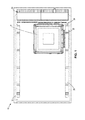
PCB 12 includes a plurality of electrical components attached thereto and electrically connected to electrically conductive traces formed on one or both major surfaces of PCB 12 or in planes or layers within PCB 12. PCB 12 and the electrical traces formed therein, thereon, or both enable electrical connection between components of PCBA, an IC in IC package 16, and electronics external to PCBA 10 via electrical connections in PCBA connector 30.
PCB 12 is also mechanically coupled to card guide rails 28. Card guide rails 28 may mechanically contact complementary card guide channels of a chassis into which PCBA 10 is inserted. In some examples, card guide rails 28 also may include a mechanism to restrain PCBA 10 relative to the chassis. For example, card guide rails 28 may include a clamping mechanism, such as a wedge lock, which can be engaged after PCBA 10 is inserted into the desired position within the chassis to reduce or substantially eliminate movement of PCBA 10 relative to the chassis. The desired position may include a position at which electrical connectors in PCBA connector 30 are electrically coupled to complementary electrical connectors on a complementary master interconnect board (MIB) or backplane connector. FIG. 3 is a conceptual and schematic diagram that illustrates an example chassis 40, card guide rails 52 a-52 f (collectively referred to herein as, “card guide rails 52”), and a MIB 60. FIG. 3 is described in additional detail below.
PCBA 10 also includes a socket 14, which is mechanically and electrically coupled to PCB 12. Socket 14 may include a plurality of electrical contacts, each of which is electrically coupled to a respective electrical trace in PCB 12. In some examples, socket 14 is a LGA socket, and includes a plurality of electrically conductive pins arranged in a complementary pattern to a plurality of electrically conductive pads on a substrate of IC package 16. Socket 14 also may define a shape configured to receive IC package 16, e.g., a complementary shape to a substrate of IC package 16. In some examples, socket 14 is a commercially available socket for connecting IC package 16 to PCB 12.
As shown in FIG. 2 , IC package 16 may include a substrate 34, an IC 36, and a package cover 38. Substrate 34 forms the mechanical and electrical contact with socket 14, and may include an electrically insulating material in which a plurality of electrically conductive traces comprising electrically conductive material are formed. The electrically conductive traces may provide pathways for signals to be transmitted between PCB 12 and IC 36. In some examples, IC package 16 includes a LGA package, and substrate 34 may define a plurality of electrically conductive pads on bottom surface 39 of substrate 34. The plurality of electrically conductive pads may form an array of pads that is substantially the same layout as the array of electrical contacts of socket 14, such that the arrays are complementary and respective ones of the plurality of electrically conductive pads contact respective ones of the plurality of electrical contacts. In this way, substrate 34 and socket 14 facilitate electrical connection between IC 36 and PCB 12. In other examples, IC package 16 may include a BGA package.
In some examples, package cover 38 includes a thermally conductive material. For example, package cover 38 may include a thermally conductive ceramic, such as AlN, SiC, Al2O3, or the like. Package cover 38 may be mechanically joined to the top surface of IC 36 using a thermally interface material, such as a thermally conductive solder, paste, or adhesive. In this way, package cover 38 may function as a heat spreader, receiving heat generated by IC 36 during operation of IC 36 and spreading the heat throughout the volume of package cover 38.
In other examples, IC package 16 may include any rigid, substantially planar device that includes at least one semiconductor die. For example, IC package 16 may include a PCB and at least one semiconductor die attached to the PCB, without a package cover 38.
In accordance with one or more examples of this application, PCBA 10 also includes a thermal cover 18. Thermal cover 18 is thermally and mechanically coupled to package cover 38, e.g., to a top surface 37 of package cover 38. Because thermal cover 18 is in thermal contact with top surface 37 of package cover 38, thermal cover 18 may receive via package cover 38 heat generated by IC 36. Thermal cover 18 may be formed of a thermally conductive, relatively stiff material, with a thickness sufficient to provide predetermined stiffness and volume to thermal cover 18. For example, thermal cover 18 may include any one or more of the following materials: aluminum, an aluminum alloy, copper, a copper alloy, a thermally conductive composite, a thermally conductive ceramic, or the like. Example aluminum alloys include an alloy including between about 60 weight percent (wt. %) and about 64 wt. % beryllium, less than about 1 wt. % oxygen, less than about 0.1 wt. % carbon, less than about 0.2 wt. % each of one or more other metal, and a balance aluminum, which is available under the trade designation AlBeMet® from Materion Brush Beryllium & Composites, Elmore, Ohio. As another example, thermal cover 18 may comprise a k-Core® heat transfer system, which includes an encapsulant material encapsulating annealed pyrolytic graphite, and is available from Thermacore, Inc., Lancaster, Pa. The encapsulant material may include aluminum, copper, magnesium, beryllium, an aluminum-beryllium alloy, a copper-molybdenum alloy, a copper-tungsten alloy, an aluminum-silicon alloy, or the like. An example thermally conductive composite may include a carbon fiber composite material.
In some examples, thermal cover 18 also mechanically presses or urges IC package 16 (e.g., substrate 34 of IC package 16) into contact with socket 14. For example, thermal cover 38 may include a plurality of apertures which receive fasteners 24. In some examples, fasteners 24 include screws, and may also include springs to mediate a force applied by the fasteners 24 against thermal cover 18 (and, indirectly, the force applied between IC package 16 and socket 14 by fasteners 24). In some examples, PCBA 10 also may include a mounting bracket 26 on an opposite side of PCB 12 from socket 14. Mounting bracket 26, Which also may be referred to as a PCB stiffener, may be formed from a relatively stiff material, such as stainless steel, another metal or alloy, a plastic, a composite, a ceramic, the like, and may receive fasteners 24. Mounting bracket 26 may be stiffer than PCB 12, and thus may deflect less under the force applied by fasteners 24 when fasteners 24 are tightened to force IC package 16 against socket 14. In this way, mounting bracket 26 may facilitate intimate thermal contact between top surface 37 of package cover 38 and thermal cover 18, as well as help maintain the electrical connections between IC package 16 and socket 14. Together, mounting bracket 26 and thermal cover 18 may stiffen PCBA 10, at least the portion of PCBA 10 proximate to socket 14, compared to a PCBA that does not include thermal cover 18 and mounting bracket 26.
As shown in FIG. 2 , a first end of thermal strap 20 may be brought into thermal contact with thermal cover 18 using one or more fasteners, such as one or more screws. In other examples, a portion of thermal strap 20 may be restrained in thermal contact with thermal cover 18 using a thermally conductive adhesive, a thermally conductive solder, a thermally conductive braze, or the like. In the example illustrated in FIGS. 1 and 2 , a second portion (e.g., end) of thermal strap 20 is coupled to CCA clamping mechanism 28. For example, CCA clamping mechanism may be clamped between CCA clamping mechanism 28 and PCB 12. In other examples, the second portion (e.g., end) of thermal strap 20 may be adhered to, soldered to, or brazed to CCA clamping mechanism 28. In other examples, the second portion (e.g., end) of thermal strap 20 may be adhered to, soldered to, brazed to, or otherwise thermally connected to another thermally conductive structure, such as a heat sink, a chassis in which PCBA 10 is disposed (see, e.g., FIG. 3 ), another PCB, or the like.
In some examples, instead of a second portion e.g., second end) of thermal strap 20 being coupled to a single structure or at a single location of a single structure, thermal strap 20 may be coupled to multiple structures, multiple locations of a single structure, or both. For example, thermal strap 20 may be partially divided (e.g., forked) to form multiple portions opposite to the first end coupled to thermal cover 18. Each portion of the multiple portions may be thermally coupled to a respective structure, such as PCB 12, CCA clamping mechanism 28, a heat sink, a chassis in which PCBA 10 is disposed (see, e.g., FIG. 3 ), another PCB, or the like. In some examples, more than one portion of the multiple portions may be thermally coupled to the same structure. For example, thermal strap 20 may be thermally coupled to PCB 12 in at least one location.
Utilizing thermal cover 18 and thermal strap 20 to provide a conductive thermal pathway from IC package 16 to another thermally conductive structure may allow use of an LGA package and socket in applications in which convection cooling of IC 36 is not practicable, such as high vacuum applications. The thermal cover 18 and thermal strap 20 may provide thermal performance comparable to or better than a BGA or CGA package that utilizes the solder connections to the PCB as the primary thermal pathway for removing heat from the IC.
This may allow use of LGA packaged components in space applications without requiring a reworking of the LGA package to a BGA CGA package, Using an LGA package may eliminate soldering of the package to the socket 14 or PCB 12, which may reduce or eliminate exposure of other components of PCBA 10 to the chemicals used in the soldering process. This may facilitate use of components that are not hermetically sealed while reducing a chance of damaging those components. In some examples, using an LGA package also may facilitate replacement of the LGA package compared to a BGA or CGA package. An LGA package also may be installed in the PCBA 10 last, which may allow functional testing and verification of the LGA package prior to installation on PCBA 10, which may facilitate manufacturing of the PCBA 10. In some examples, the LGA package also may reduce or eliminate solder fatigue due to thermal cycling of PCBA 10 during use, as no solder is used to join an LGA package to an LGA socket.
As described above, in some examples, PCBA 10 may be used in as part of a system including other PCBAs, such as a MIB or backplane. FIG. 3 is a conceptual and schematic diagram illustrating a top view of an example system 40 including a chassis 41 and a first PCBA 56 a including an integrated circuit package 66, a thermal cover 62, and a thermal strap 64. Chassis 41 may be configured to substantially fully enclose one or more PCBAs, such as PCBAs 56 a-56 c (collectively referred to herein as, “PCBAs 56”) and MIB 60 shown in FIG. 3 . In some examples, chassis 41 may separate the one or more PCBAs 56 from the environment external to the chassis 41, e.g., to protect the one or more PCBAs from environmental contaminants, physical damage, and/or electrical interference.
In the example shown in FIG. 3 , chassis 41 includes a first sidewall 42 and a second sidewall 44. First and second sidewalk 42, 44 are connected at respective ends by first end wall 46 and second end wall 48. Although not shown in FIG. 3 , chassis 41 also include a cover and a base that substantially occupies the space between the edges of sidewalk 42, 44 and end walls 46, 48, such that when fully assembled, chassis 41 forms a substantially closed container that encloses the electronics such as PCBAs 56 and MIB 60 shown in FIG. 3 ). In some examples, first and second sidewalk 42, 44 and first and second end walls 46, 48 may be formed of a metal or an alloy, such as stainless steel, aluminum, titanium, or the like. In other examples, first and second sidewalls 42, 44 and first and second end walls 46, 48 may be formed of a composite material, such as a carbon fiber composite material. In some examples, first and second sidewalls 42, 44 and first and second end walls 46, 48 may be formed of the same material. In other examples, at least one of first and second sidewalls 42, 44 and first and second end walls 46, 48 may be formed from a different material that at least one other of first and second sidewalk 42, 44 and first and second end sidewalls 46, 48. In some examples, the material from which at least one of first and second sidewalls 42, 44 and first and second end walls 46, 48 is formed may be thermally conductive.
In some examples, bracket 50 may be formed of the same material as at least one of first and second sidewalls 42, 44 and/or first and second end walls 46, 48. In other examples, bracket 50 may be formed of a different material than first and second sidewalls 42, 44 and/or first and second end walls 46, 48. As examples, bracket 50 may be formed of any one or more of aluminum, stainless steel, titanium, a composite material, or the like.
As shown in FIG. 3 , a third card guide 52 c is mounted on the interior surface of second end wall 48. In some examples, instead of being mounted on second end wall 48, third card guide 52 c may be mounted on bracket 50 or another structure within chassis 41. Fourth, fifth, and sixth card guides 52 d, 52 e, and 52 f are mounted on an interior surface of first end wall 46.
As shown in FIG. 3 , fourth card guide 52 d may be substantially aligned with first card guide 52 a to form a first card guide pair configured to receive first PCBA 56 a and substantially retain first PCBA 56 a in place relative to MIB 60 (e.g., by engaging with a CCA clamping mechanism 28 of first PCBA 56 a). The first card guide pair is substantially aligned with first electrical connector 58 a so when first PCBA 56 a is properly inserted in first card guide 52 a and fourth card guide 52 d, an electrical connector of first PCBA 56 a is aligned with and can electrically connect to first electrical connector 58 a of NUB 60. Similarly, fifth card guide 52 e may be substantially aligned with second card guide 52 b to form a second card guide pair that is substantially aligned with second electrical connector 58 b and is configured to receive a second PCBA 56 b and substantially retain second PCB 56 b in place relative to MIB 60. Sixth card guide 52 f may be substantially aligned with third card guide 52 c to form a third card guide pair that is substantially aligned with third electrical connector 58 c and is configured to receive a third PCBA 56 c and substantially retain third PCBA 56 c in place relative to MIB 60.
Although FIG. 3 illustrates a chassis 41 that includes six card guides 52 a-52 f, in other examples, chassis 41 may include a fewer or greater number of card guides 52. In some examples, at least one of card guides 52 may not be arranged or positioned in a pair with another one of card guides 52, and a single one of card guides 52 may be used to accept a PCBA, e.g., PCBA 56 a.
As shown in FIG. 3 , first PCBA 56 a includes an IC package 66 and a thermal cover 62. IC package 66 and thermal cover 62 may be similar to or substantially the same as IC package 16 and thermal cover 18 of FIGS. 1 and 2 , respectively. In contrast to the example illustrated in FIGS. 1 and 2 , the example shown in FIG. 3 includes a thermal strap 64 that is thermally coupled to thermal cover 62 and bracket 50 of chassis 41.
In some examples, rather than being coupled to bracket 50, thermal strap 64 may be thermally coupled to another component of chassis 41, such as a component of MIB 60 first sidewall 42, second sidewall 44, first end wall 46, or the like. In general, thermal strap 64 may be thermally coupled between thermal cover 62 and another thermally conductive structure, such as a heat sink, another PCB or PCBA, or the like.
The technique of FIG. 4 includes assembling IC package 16 with socket 14 (72). Socket 14 is electrically and mechanically coupled to PCB 12 of PCBA 10. Assembling IC package 16 with socket 14 (72) may include substantially aligning electrical contacts of IC package 16 with corresponding electrical contacts of socket 14. For example, IC package 16 may include an LGA package, and may include a plurality of electrically conductive pads. Socket 16 may include an LGA socket, and may include a plurality of electrically conductive pins. Assembling IC package 16 with socket 14 (72) may include substantially aligning respective ones of the plurality of electrically conductive pins with respective ones of the electrically conductive pads, and brining the respective pins and pads into contact.
The technique of FIG. 4 also may include thermally coupling thermal cover 18 to IC package 16 (74). Thermal cover 18 may mechanically urge IC package 16 (e.g., substrate 34 of IC package 16) in contact with socket 14. Further, thermal strap 20 is thermally coupled to thermal cover 18, e.g., using clamping, adhesive, soldering, brazing, or the like. In some examples, the technique may include thermally coupling thermal strap 20 to thermal cover 18. Thermal strap 20 may include a thermally conductive material, such as aluminum, copper, an aluminum alloy, a copper alloy, a thermally conductive composite, or the like.
The technique of FIG. 4 also may optionally include thermally coupling a portion of thermal strap 20 to another thermally conductive structure (76). As described above, the other thermally conductive structure may include a chassis 41 (FIG. 3 ) in which PCBA 10 is disposed, a CCA clamping mechanism 28, a MIB 60 (FIG. 3 ), a heat sink, another PCB or PCBA, or the like. In this way, the technique of FIG. 4 may form a thermal pathway between IC package 16 and a thermally conductive structure using thermal cover 18 and thermal strap 20.
Various examples have been described. These and other examples are within the scope of the following claims.
Claims (12)
1. A system comprising:
a chassis comprising a card guide;
a printed circuit board assembly (PCBA);
a circuit card assembly clamping mechanism mechanically coupled to the PCBA, wherein the circuit card assembly clamping mechanism restrains the PCBA relative to the card guide, and wherein the PCBA comprises:
a printed circuit board (PCB);
a socket mechanically and electrically coupled to the PCB;
an integrated circuit package electrically coupled to the socket;
a thermal cover comprising a thermally conductive material, wherein the thermal cover is thermally coupled to the integrated circuit package and mechanically urges the integrated circuit package in contact with the socket; and
a flexible thermal strap thermally coupled between the thermal cover and the circuit card assembly clamping mechanism, wherein the flexible thermal strap comprises a thermally conductive material.
2. The system of claim 1 , wherein the integrated circuit package comprises at least one of a land grid array (LGA) package or a ball grid array (BGA) package, wherein the at least one of the LGA package or the BGA package comprises a substrate, an integrated circuit, and a package cover, and wherein the thermal cover is thermally coupled to the package cover.
3. The system of claim 1 , wherein the thermal cover comprises at least one of a copper alloy, an aluminum alloy, a thermally conductive composite material, or a thermally conductive ceramic material.
4. The system of claim 1 , wherein the flexible thermal strap comprises at least one of copper, a copper alloy, or a thermally conductive composite material.
5. The system of claim 1 , wherein the flexible thermal strap is further mechanically and thermally coupled to at least one of a heat sink or the chassis.
6. The system of claim 1 , wherein the socket is mechanically and electrically coupled to a first side of the PCB, further comprising a mounting bracket on a second, opposite side of the PCB, wherein the thermal cover is mechanically coupled to the mounting bracket and urges the integrated circuit package in contact with the socket.
7. A method comprising:
assembling an integrated circuit package with a socket, wherein the socket is electrically coupled to a printed circuit board (PCB) of a printed circuit board assembly (PCBA); and
thermally coupling a thermal cover to the integrated circuit package, wherein the thermal cover mechanically urges the integrated circuit package in contact with the socket; and
thermally coupling a thermal strap between the thermal cover and a circuit card assembly clamping mechanism that is mechanically coupled to the PCBA wherein the flexible thermal strap comprises a thermally conductive material,
restraining the printed circuit board assembly relative to a card guide with the circuit card assembly clamping mechanism, wherein a chassis includes the card guide.
8. The method of claim 7 , further comprising:
thermally coupling the flexible thermal strap to the PCB.
9. The method of claim 8 , wherein thermally coupling the flexible thermal strap to the PCB comprises clamping a portion of the flexible thermal strap between the circuit card assembly clamping mechanism and the PCB.
10. The method of claim 7 , further comprising:
mechanically and thermally coupling the flexible thermal strap to the chassis.
11. The method of claim 7 , wherein the integrated circuit package comprises at least one of a land grid array (LGA) package or a ball grid array (BGA) package, wherein the at least one of the LGA package or the BGA package comprises a substrate, an integrated circuit, and a package cover, and wherein thermally coupling the thermal cover to the integrated circuit package comprises thermally coupling the thermal cover to the package cover.
12. The PCBA of claim 7 , wherein the thermal cover comprises at least one of a copper alloy, an aluminum alloy, a thermally conductive composite material, or a thermally conductive ceramic, and wherein the flexible thermal strap comprises at least one of copper, a copper alloy, or a thermally conductive composite material.
Priority Applications (2)
| Application Number | Priority Date | Filing Date | Title |
|---|---|---|---|
| US14/453,333 US9818669B2 (en) | 2014-08-06 | 2014-08-06 | Printed circuit board assembly including conductive heat transfer |
| EP15178741.3A EP2983202B1 (en) | 2014-08-06 | 2015-07-28 | Printed circuit board assembly including conductive heat transfer |
Applications Claiming Priority (1)
| Application Number | Priority Date | Filing Date | Title |
|---|---|---|---|
| US14/453,333 US9818669B2 (en) | 2014-08-06 | 2014-08-06 | Printed circuit board assembly including conductive heat transfer |
Publications (2)
| Publication Number | Publication Date |
|---|---|
| US20160043017A1 US20160043017A1 (en) | 2016-02-11 |
| US9818669B2 true US9818669B2 (en) | 2017-11-14 |
Family
ID=53724137
Family Applications (1)
| Application Number | Title | Priority Date | Filing Date |
|---|---|---|---|
| US14/453,333 Active 2035-09-08 US9818669B2 (en) | 2014-08-06 | 2014-08-06 | Printed circuit board assembly including conductive heat transfer |
Country Status (2)
| Country | Link |
|---|---|
| US (1) | US9818669B2 (en) |
| EP (1) | EP2983202B1 (en) |
Cited By (2)
| Publication number | Priority date | Publication date | Assignee | Title |
|---|---|---|---|---|
| US11195779B2 (en) | 2019-08-09 | 2021-12-07 | Raytheon Company | Electronic module for motherboard |
| US11885747B2 (en) | 2020-02-21 | 2024-01-30 | Ecolab Usa Inc. | Modular optical sensor |
Families Citing this family (8)
| Publication number | Priority date | Publication date | Assignee | Title |
|---|---|---|---|---|
| US10225953B2 (en) * | 2014-10-31 | 2019-03-05 | Thermal Corp. | Vehicle thermal management system |
| US9590329B2 (en) | 2015-06-08 | 2017-03-07 | International Business Machines Corporation | Pin attach converter |
| FR3047865B1 (en) * | 2016-02-12 | 2021-03-05 | Continental Automotive France | PROTECTION BOX FOR A COMPUTER AND METHOD FOR MANUFACTURING SUCH A BOX |
| US10108073B2 (en) | 2017-03-10 | 2018-10-23 | Google Llc | Heat transfer from image sensor |
| US10952352B2 (en) * | 2017-10-27 | 2021-03-16 | Micron Technology, Inc. | Assemblies including heat dispersing elements and related systems and methods |
| US10566313B1 (en) | 2018-08-21 | 2020-02-18 | International Business Machines Corporation | Integrated circuit chip carrier with in-plane thermal conductance layer |
| US11929297B2 (en) * | 2020-11-09 | 2024-03-12 | Hamilton Sundstrand Corporation | Conductive thermal management architecture for electronic devices |
| US20210208647A1 (en) * | 2021-02-26 | 2021-07-08 | Intel Corporation | Flexible and modular top and bottom side processor unit module cooling |
Citations (28)
| Publication number | Priority date | Publication date | Assignee | Title |
|---|---|---|---|---|
| US5802707A (en) * | 1996-03-28 | 1998-09-08 | Intel Corporation | Controlled bondline thickness attachment mechanism |
| US5898219A (en) | 1997-04-02 | 1999-04-27 | Intel Corporation | Custom corner attach heat sink design for a plastic ball grid array integrated circuit package |
| US6449155B1 (en) | 2001-08-09 | 2002-09-10 | International Business Machines Corporation | Land grid array subassembly for multichip modules |
| US6490161B1 (en) | 2002-01-08 | 2002-12-03 | International Business Machines Corporation | Peripheral land grid array package with improved thermal performance |
| US6504243B1 (en) | 2000-04-07 | 2003-01-07 | Advanced Micro Devices, Inc. | Removable heat transfer apparatus for a pin grid array (PGA) device, and associated installation and removal methods |
| US6716676B2 (en) | 2001-06-04 | 2004-04-06 | Siliconware Precision Industries Co., Ltd. | Thermally-enhanced stacked-die ball grid array semiconductor package and method of fabricating the same |
| US20040257786A1 (en) * | 2003-06-05 | 2004-12-23 | Osamu Murasawa | Electronic device, information processor, and electromagnetic radiation suppressing member |
| US20050068740A1 (en) * | 2003-09-26 | 2005-03-31 | Ulen Neal E. | Heat sink mounting and interface mechanism and method of assembling same |
| US7134881B1 (en) | 2005-12-14 | 2006-11-14 | Fujitsu Limited | Land grid array connector and package mount structure |
| US20060268525A1 (en) | 2005-05-31 | 2006-11-30 | Kwang-Jin Jeong | Display module |
| US7251138B2 (en) | 2004-08-24 | 2007-07-31 | Tyco Electronics Corporation | Thermal managed interconnect system for a circuit board |
| US7269015B2 (en) | 2005-02-01 | 2007-09-11 | Tyco Electronics Corporation | Heat sink interface insert |
| US20070236888A1 (en) * | 2006-04-11 | 2007-10-11 | International Business Machines Corporation | System and method for cooling a module |
| US7304381B2 (en) | 2003-05-28 | 2007-12-04 | Intel Corporation | Package and method for attaching an integrated heat spreader |
| US7428154B2 (en) * | 2002-09-18 | 2008-09-23 | Fujitsu Limited | Package structure, printed circuit board mounted with the same, electronic apparatus having the printed circuit board |
| US20090093142A1 (en) * | 2007-10-09 | 2009-04-09 | Hon Hai Precision Ind. Co., Ltd. | Electrical connector assembly with fastening element |
| US20090096086A1 (en) * | 2007-10-15 | 2009-04-16 | Venkat Natarajan | Cooling system for semiconductor devices |
| US20090283902A1 (en) * | 2008-05-13 | 2009-11-19 | Raschid Jose Bezama | Semiconductor Package Structures Having Liquid Coolers Integrated with First Level Chip Package Modules |
| US20100321890A1 (en) | 2009-06-19 | 2010-12-23 | General Electric Company | Avionics Chassis |
| US7957148B1 (en) * | 2009-12-08 | 2011-06-07 | International Business Machines Corporation | Low profile computer processor retention device |
| US7980861B2 (en) * | 2007-10-24 | 2011-07-19 | Fujitsu Limited | Printed circuit board unit and socket |
| US8008133B2 (en) | 2008-02-11 | 2011-08-30 | Globalfoundries Inc. | Chip package with channel stiffener frame |
| US20120307471A1 (en) * | 2011-06-01 | 2012-12-06 | Honeywell International Inc. | Thermally conductive and electrically insulative card guide |
| US8345431B2 (en) | 2008-01-02 | 2013-01-01 | Microelectronics Assembly Technologies, Inc. | Thin multi-chip flex module |
| US20130147028A1 (en) | 2011-12-07 | 2013-06-13 | Michael Z. Su | Heat spreader for multiple chip systems |
| US20130148305A1 (en) * | 2011-12-08 | 2013-06-13 | Oracle International Corporation | Design of a heat dissipation structure for an integrated circuit (ic) chip |
| US8493738B2 (en) | 2011-05-06 | 2013-07-23 | International Business Machines Corporation | Cooled electronic system with thermal spreaders coupling electronics cards to cold rails |
| US8537552B2 (en) | 2009-09-25 | 2013-09-17 | Raytheon Company | Heat sink interface having three-dimensional tolerance compensation |
-
2014
- 2014-08-06 US US14/453,333 patent/US9818669B2/en active Active
-
2015
- 2015-07-28 EP EP15178741.3A patent/EP2983202B1/en active Active
Patent Citations (29)
| Publication number | Priority date | Publication date | Assignee | Title |
|---|---|---|---|---|
| US5802707A (en) * | 1996-03-28 | 1998-09-08 | Intel Corporation | Controlled bondline thickness attachment mechanism |
| US5898219A (en) | 1997-04-02 | 1999-04-27 | Intel Corporation | Custom corner attach heat sink design for a plastic ball grid array integrated circuit package |
| US6504243B1 (en) | 2000-04-07 | 2003-01-07 | Advanced Micro Devices, Inc. | Removable heat transfer apparatus for a pin grid array (PGA) device, and associated installation and removal methods |
| US6716676B2 (en) | 2001-06-04 | 2004-04-06 | Siliconware Precision Industries Co., Ltd. | Thermally-enhanced stacked-die ball grid array semiconductor package and method of fabricating the same |
| US6449155B1 (en) | 2001-08-09 | 2002-09-10 | International Business Machines Corporation | Land grid array subassembly for multichip modules |
| US6490161B1 (en) | 2002-01-08 | 2002-12-03 | International Business Machines Corporation | Peripheral land grid array package with improved thermal performance |
| US7428154B2 (en) * | 2002-09-18 | 2008-09-23 | Fujitsu Limited | Package structure, printed circuit board mounted with the same, electronic apparatus having the printed circuit board |
| US7304381B2 (en) | 2003-05-28 | 2007-12-04 | Intel Corporation | Package and method for attaching an integrated heat spreader |
| US20040257786A1 (en) * | 2003-06-05 | 2004-12-23 | Osamu Murasawa | Electronic device, information processor, and electromagnetic radiation suppressing member |
| US7053295B2 (en) | 2003-06-05 | 2006-05-30 | Sony Computer Entertainment, Inc. | Electronic device, information processor, and electromagnetic radiation suppressing member |
| US20050068740A1 (en) * | 2003-09-26 | 2005-03-31 | Ulen Neal E. | Heat sink mounting and interface mechanism and method of assembling same |
| US7251138B2 (en) | 2004-08-24 | 2007-07-31 | Tyco Electronics Corporation | Thermal managed interconnect system for a circuit board |
| US7269015B2 (en) | 2005-02-01 | 2007-09-11 | Tyco Electronics Corporation | Heat sink interface insert |
| US20060268525A1 (en) | 2005-05-31 | 2006-11-30 | Kwang-Jin Jeong | Display module |
| US7134881B1 (en) | 2005-12-14 | 2006-11-14 | Fujitsu Limited | Land grid array connector and package mount structure |
| US20070236888A1 (en) * | 2006-04-11 | 2007-10-11 | International Business Machines Corporation | System and method for cooling a module |
| US20090093142A1 (en) * | 2007-10-09 | 2009-04-09 | Hon Hai Precision Ind. Co., Ltd. | Electrical connector assembly with fastening element |
| US20090096086A1 (en) * | 2007-10-15 | 2009-04-16 | Venkat Natarajan | Cooling system for semiconductor devices |
| US7980861B2 (en) * | 2007-10-24 | 2011-07-19 | Fujitsu Limited | Printed circuit board unit and socket |
| US8345431B2 (en) | 2008-01-02 | 2013-01-01 | Microelectronics Assembly Technologies, Inc. | Thin multi-chip flex module |
| US8008133B2 (en) | 2008-02-11 | 2011-08-30 | Globalfoundries Inc. | Chip package with channel stiffener frame |
| US20090283902A1 (en) * | 2008-05-13 | 2009-11-19 | Raschid Jose Bezama | Semiconductor Package Structures Having Liquid Coolers Integrated with First Level Chip Package Modules |
| US20100321890A1 (en) | 2009-06-19 | 2010-12-23 | General Electric Company | Avionics Chassis |
| US8537552B2 (en) | 2009-09-25 | 2013-09-17 | Raytheon Company | Heat sink interface having three-dimensional tolerance compensation |
| US7957148B1 (en) * | 2009-12-08 | 2011-06-07 | International Business Machines Corporation | Low profile computer processor retention device |
| US8493738B2 (en) | 2011-05-06 | 2013-07-23 | International Business Machines Corporation | Cooled electronic system with thermal spreaders coupling electronics cards to cold rails |
| US20120307471A1 (en) * | 2011-06-01 | 2012-12-06 | Honeywell International Inc. | Thermally conductive and electrically insulative card guide |
| US20130147028A1 (en) | 2011-12-07 | 2013-06-13 | Michael Z. Su | Heat spreader for multiple chip systems |
| US20130148305A1 (en) * | 2011-12-08 | 2013-06-13 | Oracle International Corporation | Design of a heat dissipation structure for an integrated circuit (ic) chip |
Non-Patent Citations (4)
| Title |
|---|
| Communication pursuant to Article 94(3) EPC from counterpart European Application No. 15178741.3, dated Apr. 4, 2017, 5 pp. |
| Extended Search Report from counterpart European Application No. 15178741.3, dated Dec. 18, 2015, 8 pp. |
| Response to EPC Communication from counterpart European Application No. EP 15178741.3, filed on Aug. 22, 2017, 6 pp. |
| Response to the Extended Search Report dated Dec. 18, 2015, from counterpart European Application No. 15178741.3 filed Jul. 18, 2016, 15 pp. |
Cited By (2)
| Publication number | Priority date | Publication date | Assignee | Title |
|---|---|---|---|---|
| US11195779B2 (en) | 2019-08-09 | 2021-12-07 | Raytheon Company | Electronic module for motherboard |
| US11885747B2 (en) | 2020-02-21 | 2024-01-30 | Ecolab Usa Inc. | Modular optical sensor |
Also Published As
| Publication number | Publication date |
|---|---|
| EP2983202B1 (en) | 2019-03-27 |
| EP2983202A1 (en) | 2016-02-10 |
| US20160043017A1 (en) | 2016-02-11 |
Similar Documents
| Publication | Publication Date | Title |
|---|---|---|
| US9818669B2 (en) | Printed circuit board assembly including conductive heat transfer | |
| US6459582B1 (en) | Heatsink apparatus for de-coupling clamping forces on an integrated circuit package | |
| KR100833185B1 (en) | heatsink and memory module using the same | |
| US6816378B1 (en) | Stack up assembly | |
| JP5116278B2 (en) | Method and apparatus for optimizing heat transfer by electronic components | |
| US8879263B2 (en) | Conducting heat away from a printed circuit board assembly in an enclosure | |
| KR101388792B1 (en) | Semiconductor package module | |
| US6853068B1 (en) | Heatsinking and packaging of integrated circuit chips | |
| CN210668339U (en) | Electronic device | |
| US9082645B2 (en) | Manufacturing method of semiconductor module | |
| US20070236888A1 (en) | System and method for cooling a module | |
| US9883612B2 (en) | Heat sink attachment on existing heat sinks | |
| JP2008305838A (en) | Semiconductor device and mounting structure thereof | |
| US10440811B2 (en) | Active heatsink lid | |
| KR100389920B1 (en) | Semiconductor module improving a reliability deterioration due to coefficient of thermal expansion | |
| US9147630B2 (en) | Power semiconductor assembly and module | |
| US20230239994A1 (en) | Electronic assemblies having embedded passive heat pipes and associated method | |
| US20210111093A1 (en) | Heterogeneous Lid Seal Band for Structural Stability in Multiple Integrated Circuit (IC) Device Modules | |
| KR100630013B1 (en) | Solder-free pcb assembly | |
| US20230067409A1 (en) | Damper system for a lidless integrated circuit | |
| KR20160112345A (en) | Semiconductor chip | |
| US20210028079A1 (en) | Integrated Circuit (IC) Device Package Lid Attach Utilizing Nano Particle Metallic Paste | |
| JPWO2004112450A1 (en) | Substrate mounting method and mounting structure | |
| US8407888B2 (en) | Method of assembling a circuit board assembly | |
| JPH01230260A (en) | Cooling structure for semiconductor package |
Legal Events
| Date | Code | Title | Description |
|---|---|---|---|
| AS | Assignment |
Owner name: HONEYWELL INTERNATIONAL INC., PATENT SERVICES M/S Free format text: ASSIGNMENT OF ASSIGNORS INTEREST;ASSIGNORS:JONES, KIRK;KREIDER, THOM;JACKSON, LARRY;SIGNING DATES FROM 20140729 TO 20140805;REEL/FRAME:033479/0606 |
|
| STCF | Information on status: patent grant |
Free format text: PATENTED CASE |
|
| MAFP | Maintenance fee payment |
Free format text: PAYMENT OF MAINTENANCE FEE, 4TH YEAR, LARGE ENTITY (ORIGINAL EVENT CODE: M1551); ENTITY STATUS OF PATENT OWNER: LARGE ENTITY Year of fee payment: 4 |