US9799626B2 - Semiconductor packages and other circuit modules with porous and non-porous stabilizing layers - Google Patents
Semiconductor packages and other circuit modules with porous and non-porous stabilizing layers Download PDFInfo
- Publication number
- US9799626B2 US9799626B2 US14/852,855 US201514852855A US9799626B2 US 9799626 B2 US9799626 B2 US 9799626B2 US 201514852855 A US201514852855 A US 201514852855A US 9799626 B2 US9799626 B2 US 9799626B2
- Authority
- US
- United States
- Prior art keywords
- layer
- modules
- contact pads
- module
- areas
- Prior art date
- Legal status (The legal status is an assumption and is not a legal conclusion. Google has not performed a legal analysis and makes no representation as to the accuracy of the status listed.)
- Active
Links
Images


Classifications
-
- H—ELECTRICITY
- H01—ELECTRIC ELEMENTS
- H01L—SEMICONDUCTOR DEVICES NOT COVERED BY CLASS H10
- H01L24/00—Arrangements for connecting or disconnecting semiconductor or solid-state bodies; Methods or apparatus related thereto
- H01L24/93—Batch processes
- H01L24/95—Batch processes at chip-level, i.e. with connecting carried out on a plurality of singulated devices, i.e. on diced chips
- H01L24/97—Batch processes at chip-level, i.e. with connecting carried out on a plurality of singulated devices, i.e. on diced chips the devices being connected to a common substrate, e.g. interposer, said common substrate being separable into individual assemblies after connecting
-
- H—ELECTRICITY
- H01—ELECTRIC ELEMENTS
- H01L—SEMICONDUCTOR DEVICES NOT COVERED BY CLASS H10
- H01L21/00—Processes or apparatus adapted for the manufacture or treatment of semiconductor or solid state devices or of parts thereof
- H01L21/02—Manufacture or treatment of semiconductor devices or of parts thereof
- H01L21/04—Manufacture or treatment of semiconductor devices or of parts thereof the devices having at least one potential-jump barrier or surface barrier, e.g. PN junction, depletion layer or carrier concentration layer
- H01L21/18—Manufacture or treatment of semiconductor devices or of parts thereof the devices having at least one potential-jump barrier or surface barrier, e.g. PN junction, depletion layer or carrier concentration layer the devices having semiconductor bodies comprising elements of Group IV of the Periodic System or AIIIBV compounds with or without impurities, e.g. doping materials
- H01L21/30—Treatment of semiconductor bodies using processes or apparatus not provided for in groups H01L21/20 - H01L21/26
- H01L21/31—Treatment of semiconductor bodies using processes or apparatus not provided for in groups H01L21/20 - H01L21/26 to form insulating layers thereon, e.g. for masking or by using photolithographic techniques; After treatment of these layers; Selection of materials for these layers
- H01L21/3205—Deposition of non-insulating-, e.g. conductive- or resistive-, layers on insulating layers; After-treatment of these layers
- H01L21/321—After treatment
- H01L21/3213—Physical or chemical etching of the layers, e.g. to produce a patterned layer from a pre-deposited extensive layer
- H01L21/32133—Physical or chemical etching of the layers, e.g. to produce a patterned layer from a pre-deposited extensive layer by chemical means only
-
- H—ELECTRICITY
- H01—ELECTRIC ELEMENTS
- H01L—SEMICONDUCTOR DEVICES NOT COVERED BY CLASS H10
- H01L21/00—Processes or apparatus adapted for the manufacture or treatment of semiconductor or solid state devices or of parts thereof
- H01L21/02—Manufacture or treatment of semiconductor devices or of parts thereof
- H01L21/04—Manufacture or treatment of semiconductor devices or of parts thereof the devices having at least one potential-jump barrier or surface barrier, e.g. PN junction, depletion layer or carrier concentration layer
- H01L21/48—Manufacture or treatment of parts, e.g. containers, prior to assembly of the devices, using processes not provided for in a single one of the subgroups H01L21/06 - H01L21/326
- H01L21/4814—Conductive parts
- H01L21/4846—Leads on or in insulating or insulated substrates, e.g. metallisation
- H01L21/486—Via connections through the substrate with or without pins
-
- H—ELECTRICITY
- H01—ELECTRIC ELEMENTS
- H01L—SEMICONDUCTOR DEVICES NOT COVERED BY CLASS H10
- H01L21/00—Processes or apparatus adapted for the manufacture or treatment of semiconductor or solid state devices or of parts thereof
- H01L21/02—Manufacture or treatment of semiconductor devices or of parts thereof
- H01L21/04—Manufacture or treatment of semiconductor devices or of parts thereof the devices having at least one potential-jump barrier or surface barrier, e.g. PN junction, depletion layer or carrier concentration layer
- H01L21/50—Assembly of semiconductor devices using processes or apparatus not provided for in a single one of the subgroups H01L21/06 - H01L21/326, e.g. sealing of a cap to a base of a container
- H01L21/56—Encapsulations, e.g. encapsulation layers, coatings
- H01L21/561—Batch processing
-
- H—ELECTRICITY
- H01—ELECTRIC ELEMENTS
- H01L—SEMICONDUCTOR DEVICES NOT COVERED BY CLASS H10
- H01L21/00—Processes or apparatus adapted for the manufacture or treatment of semiconductor or solid state devices or of parts thereof
- H01L21/70—Manufacture or treatment of devices consisting of a plurality of solid state components formed in or on a common substrate or of parts thereof; Manufacture of integrated circuit devices or of parts thereof
- H01L21/77—Manufacture or treatment of devices consisting of a plurality of solid state components or integrated circuits formed in, or on, a common substrate
- H01L21/78—Manufacture or treatment of devices consisting of a plurality of solid state components or integrated circuits formed in, or on, a common substrate with subsequent division of the substrate into plural individual devices
- H01L21/82—Manufacture or treatment of devices consisting of a plurality of solid state components or integrated circuits formed in, or on, a common substrate with subsequent division of the substrate into plural individual devices to produce devices, e.g. integrated circuits, each consisting of a plurality of components
- H01L21/822—Manufacture or treatment of devices consisting of a plurality of solid state components or integrated circuits formed in, or on, a common substrate with subsequent division of the substrate into plural individual devices to produce devices, e.g. integrated circuits, each consisting of a plurality of components the substrate being a semiconductor, using silicon technology
-
- H—ELECTRICITY
- H01—ELECTRIC ELEMENTS
- H01L—SEMICONDUCTOR DEVICES NOT COVERED BY CLASS H10
- H01L23/00—Details of semiconductor or other solid state devices
- H01L23/28—Encapsulations, e.g. encapsulating layers, coatings, e.g. for protection
- H01L23/31—Encapsulations, e.g. encapsulating layers, coatings, e.g. for protection characterised by the arrangement or shape
- H01L23/3107—Encapsulations, e.g. encapsulating layers, coatings, e.g. for protection characterised by the arrangement or shape the device being completely enclosed
- H01L23/3121—Encapsulations, e.g. encapsulating layers, coatings, e.g. for protection characterised by the arrangement or shape the device being completely enclosed a substrate forming part of the encapsulation
- H01L23/3128—Encapsulations, e.g. encapsulating layers, coatings, e.g. for protection characterised by the arrangement or shape the device being completely enclosed a substrate forming part of the encapsulation the substrate having spherical bumps for external connection
-
- H—ELECTRICITY
- H01—ELECTRIC ELEMENTS
- H01L—SEMICONDUCTOR DEVICES NOT COVERED BY CLASS H10
- H01L23/00—Details of semiconductor or other solid state devices
- H01L23/28—Encapsulations, e.g. encapsulating layers, coatings, e.g. for protection
- H01L23/31—Encapsulations, e.g. encapsulating layers, coatings, e.g. for protection characterised by the arrangement or shape
- H01L23/3107—Encapsulations, e.g. encapsulating layers, coatings, e.g. for protection characterised by the arrangement or shape the device being completely enclosed
- H01L23/3135—Double encapsulation or coating and encapsulation
-
- H—ELECTRICITY
- H01—ELECTRIC ELEMENTS
- H01L—SEMICONDUCTOR DEVICES NOT COVERED BY CLASS H10
- H01L23/00—Details of semiconductor or other solid state devices
- H01L23/28—Encapsulations, e.g. encapsulating layers, coatings, e.g. for protection
- H01L23/31—Encapsulations, e.g. encapsulating layers, coatings, e.g. for protection characterised by the arrangement or shape
- H01L23/3107—Encapsulations, e.g. encapsulating layers, coatings, e.g. for protection characterised by the arrangement or shape the device being completely enclosed
- H01L23/3142—Sealing arrangements between parts, e.g. adhesion promotors
-
- H—ELECTRICITY
- H01—ELECTRIC ELEMENTS
- H01L—SEMICONDUCTOR DEVICES NOT COVERED BY CLASS H10
- H01L23/00—Details of semiconductor or other solid state devices
- H01L23/48—Arrangements for conducting electric current to or from the solid state body in operation, e.g. leads, terminal arrangements ; Selection of materials therefor
- H01L23/488—Arrangements for conducting electric current to or from the solid state body in operation, e.g. leads, terminal arrangements ; Selection of materials therefor consisting of soldered or bonded constructions
- H01L23/498—Leads, i.e. metallisations or lead-frames on insulating substrates, e.g. chip carriers
- H01L23/49827—Via connections through the substrates, e.g. pins going through the substrate, coaxial cables
-
- H—ELECTRICITY
- H01—ELECTRIC ELEMENTS
- H01L—SEMICONDUCTOR DEVICES NOT COVERED BY CLASS H10
- H01L23/00—Details of semiconductor or other solid state devices
- H01L23/52—Arrangements for conducting electric current within the device in operation from one component to another, i.e. interconnections, e.g. wires, lead frames
- H01L23/538—Arrangements for conducting electric current within the device in operation from one component to another, i.e. interconnections, e.g. wires, lead frames the interconnection structure between a plurality of semiconductor chips being formed on, or in, insulating substrates
- H01L23/5384—Conductive vias through the substrate with or without pins, e.g. buried coaxial conductors
-
- H—ELECTRICITY
- H01—ELECTRIC ELEMENTS
- H01L—SEMICONDUCTOR DEVICES NOT COVERED BY CLASS H10
- H01L24/00—Arrangements for connecting or disconnecting semiconductor or solid-state bodies; Methods or apparatus related thereto
- H01L24/73—Means for bonding being of different types provided for in two or more of groups H01L24/10, H01L24/18, H01L24/26, H01L24/34, H01L24/42, H01L24/50, H01L24/63, H01L24/71
-
- H—ELECTRICITY
- H01—ELECTRIC ELEMENTS
- H01L—SEMICONDUCTOR DEVICES NOT COVERED BY CLASS H10
- H01L25/00—Assemblies consisting of a plurality of individual semiconductor or other solid state devices ; Multistep manufacturing processes thereof
- H01L25/03—Assemblies consisting of a plurality of individual semiconductor or other solid state devices ; Multistep manufacturing processes thereof all the devices being of a type provided for in the same subgroup of groups H01L27/00 - H01L33/00, or in a single subclass of H10K, H10N, e.g. assemblies of rectifier diodes
- H01L25/04—Assemblies consisting of a plurality of individual semiconductor or other solid state devices ; Multistep manufacturing processes thereof all the devices being of a type provided for in the same subgroup of groups H01L27/00 - H01L33/00, or in a single subclass of H10K, H10N, e.g. assemblies of rectifier diodes the devices not having separate containers
- H01L25/07—Assemblies consisting of a plurality of individual semiconductor or other solid state devices ; Multistep manufacturing processes thereof all the devices being of a type provided for in the same subgroup of groups H01L27/00 - H01L33/00, or in a single subclass of H10K, H10N, e.g. assemblies of rectifier diodes the devices not having separate containers the devices being of a type provided for in group H01L29/00
- H01L25/072—Assemblies consisting of a plurality of individual semiconductor or other solid state devices ; Multistep manufacturing processes thereof all the devices being of a type provided for in the same subgroup of groups H01L27/00 - H01L33/00, or in a single subclass of H10K, H10N, e.g. assemblies of rectifier diodes the devices not having separate containers the devices being of a type provided for in group H01L29/00 the devices being arranged next to each other
-
- H—ELECTRICITY
- H01—ELECTRIC ELEMENTS
- H01L—SEMICONDUCTOR DEVICES NOT COVERED BY CLASS H10
- H01L25/00—Assemblies consisting of a plurality of individual semiconductor or other solid state devices ; Multistep manufacturing processes thereof
- H01L25/03—Assemblies consisting of a plurality of individual semiconductor or other solid state devices ; Multistep manufacturing processes thereof all the devices being of a type provided for in the same subgroup of groups H01L27/00 - H01L33/00, or in a single subclass of H10K, H10N, e.g. assemblies of rectifier diodes
- H01L25/10—Assemblies consisting of a plurality of individual semiconductor or other solid state devices ; Multistep manufacturing processes thereof all the devices being of a type provided for in the same subgroup of groups H01L27/00 - H01L33/00, or in a single subclass of H10K, H10N, e.g. assemblies of rectifier diodes the devices having separate containers
- H01L25/11—Assemblies consisting of a plurality of individual semiconductor or other solid state devices ; Multistep manufacturing processes thereof all the devices being of a type provided for in the same subgroup of groups H01L27/00 - H01L33/00, or in a single subclass of H10K, H10N, e.g. assemblies of rectifier diodes the devices having separate containers the devices being of a type provided for in group H01L29/00
- H01L25/115—Assemblies consisting of a plurality of individual semiconductor or other solid state devices ; Multistep manufacturing processes thereof all the devices being of a type provided for in the same subgroup of groups H01L27/00 - H01L33/00, or in a single subclass of H10K, H10N, e.g. assemblies of rectifier diodes the devices having separate containers the devices being of a type provided for in group H01L29/00 the devices being arranged next to each other
-
- H—ELECTRICITY
- H01—ELECTRIC ELEMENTS
- H01L—SEMICONDUCTOR DEVICES NOT COVERED BY CLASS H10
- H01L25/00—Assemblies consisting of a plurality of individual semiconductor or other solid state devices ; Multistep manufacturing processes thereof
- H01L25/50—Multistep manufacturing processes of assemblies consisting of devices, each device being of a type provided for in group H01L27/00 or H01L29/00
-
- H—ELECTRICITY
- H01—ELECTRIC ELEMENTS
- H01L—SEMICONDUCTOR DEVICES NOT COVERED BY CLASS H10
- H01L2224/00—Indexing scheme for arrangements for connecting or disconnecting semiconductor or solid-state bodies and methods related thereto as covered by H01L24/00
- H01L2224/01—Means for bonding being attached to, or being formed on, the surface to be connected, e.g. chip-to-package, die-attach, "first-level" interconnects; Manufacturing methods related thereto
- H01L2224/10—Bump connectors; Manufacturing methods related thereto
- H01L2224/12—Structure, shape, material or disposition of the bump connectors prior to the connecting process
- H01L2224/13—Structure, shape, material or disposition of the bump connectors prior to the connecting process of an individual bump connector
- H01L2224/13001—Core members of the bump connector
- H01L2224/13099—Material
- H01L2224/131—Material with a principal constituent of the material being a metal or a metalloid, e.g. boron [B], silicon [Si], germanium [Ge], arsenic [As], antimony [Sb], tellurium [Te] and polonium [Po], and alloys thereof
-
- H—ELECTRICITY
- H01—ELECTRIC ELEMENTS
- H01L—SEMICONDUCTOR DEVICES NOT COVERED BY CLASS H10
- H01L2224/00—Indexing scheme for arrangements for connecting or disconnecting semiconductor or solid-state bodies and methods related thereto as covered by H01L24/00
- H01L2224/01—Means for bonding being attached to, or being formed on, the surface to be connected, e.g. chip-to-package, die-attach, "first-level" interconnects; Manufacturing methods related thereto
- H01L2224/10—Bump connectors; Manufacturing methods related thereto
- H01L2224/15—Structure, shape, material or disposition of the bump connectors after the connecting process
- H01L2224/16—Structure, shape, material or disposition of the bump connectors after the connecting process of an individual bump connector
- H01L2224/161—Disposition
- H01L2224/16151—Disposition the bump connector connecting between a semiconductor or solid-state body and an item not being a semiconductor or solid-state body, e.g. chip-to-substrate, chip-to-passive
- H01L2224/16221—Disposition the bump connector connecting between a semiconductor or solid-state body and an item not being a semiconductor or solid-state body, e.g. chip-to-substrate, chip-to-passive the body and the item being stacked
- H01L2224/16225—Disposition the bump connector connecting between a semiconductor or solid-state body and an item not being a semiconductor or solid-state body, e.g. chip-to-substrate, chip-to-passive the body and the item being stacked the item being non-metallic, e.g. insulating substrate with or without metallisation
- H01L2224/16227—Disposition the bump connector connecting between a semiconductor or solid-state body and an item not being a semiconductor or solid-state body, e.g. chip-to-substrate, chip-to-passive the body and the item being stacked the item being non-metallic, e.g. insulating substrate with or without metallisation the bump connector connecting to a bond pad of the item
-
- H—ELECTRICITY
- H01—ELECTRIC ELEMENTS
- H01L—SEMICONDUCTOR DEVICES NOT COVERED BY CLASS H10
- H01L2224/00—Indexing scheme for arrangements for connecting or disconnecting semiconductor or solid-state bodies and methods related thereto as covered by H01L24/00
- H01L2224/01—Means for bonding being attached to, or being formed on, the surface to be connected, e.g. chip-to-package, die-attach, "first-level" interconnects; Manufacturing methods related thereto
- H01L2224/26—Layer connectors, e.g. plate connectors, solder or adhesive layers; Manufacturing methods related thereto
- H01L2224/28—Structure, shape, material or disposition of the layer connectors prior to the connecting process
- H01L2224/29—Structure, shape, material or disposition of the layer connectors prior to the connecting process of an individual layer connector
- H01L2224/29001—Core members of the layer connector
- H01L2224/29099—Material
- H01L2224/2919—Material with a principal constituent of the material being a polymer, e.g. polyester, phenolic based polymer, epoxy
-
- H—ELECTRICITY
- H01—ELECTRIC ELEMENTS
- H01L—SEMICONDUCTOR DEVICES NOT COVERED BY CLASS H10
- H01L2224/00—Indexing scheme for arrangements for connecting or disconnecting semiconductor or solid-state bodies and methods related thereto as covered by H01L24/00
- H01L2224/01—Means for bonding being attached to, or being formed on, the surface to be connected, e.g. chip-to-package, die-attach, "first-level" interconnects; Manufacturing methods related thereto
- H01L2224/26—Layer connectors, e.g. plate connectors, solder or adhesive layers; Manufacturing methods related thereto
- H01L2224/28—Structure, shape, material or disposition of the layer connectors prior to the connecting process
- H01L2224/29—Structure, shape, material or disposition of the layer connectors prior to the connecting process of an individual layer connector
- H01L2224/29001—Core members of the layer connector
- H01L2224/29099—Material
- H01L2224/29198—Material with a principal constituent of the material being a combination of two or more materials in the form of a matrix with a filler, i.e. being a hybrid material, e.g. segmented structures, foams
- H01L2224/29199—Material of the matrix
- H01L2224/2929—Material of the matrix with a principal constituent of the material being a polymer, e.g. polyester, phenolic based polymer, epoxy
-
- H—ELECTRICITY
- H01—ELECTRIC ELEMENTS
- H01L—SEMICONDUCTOR DEVICES NOT COVERED BY CLASS H10
- H01L2224/00—Indexing scheme for arrangements for connecting or disconnecting semiconductor or solid-state bodies and methods related thereto as covered by H01L24/00
- H01L2224/01—Means for bonding being attached to, or being formed on, the surface to be connected, e.g. chip-to-package, die-attach, "first-level" interconnects; Manufacturing methods related thereto
- H01L2224/26—Layer connectors, e.g. plate connectors, solder or adhesive layers; Manufacturing methods related thereto
- H01L2224/28—Structure, shape, material or disposition of the layer connectors prior to the connecting process
- H01L2224/29—Structure, shape, material or disposition of the layer connectors prior to the connecting process of an individual layer connector
- H01L2224/29001—Core members of the layer connector
- H01L2224/29099—Material
- H01L2224/29198—Material with a principal constituent of the material being a combination of two or more materials in the form of a matrix with a filler, i.e. being a hybrid material, e.g. segmented structures, foams
- H01L2224/29298—Fillers
- H01L2224/29299—Base material
-
- H—ELECTRICITY
- H01—ELECTRIC ELEMENTS
- H01L—SEMICONDUCTOR DEVICES NOT COVERED BY CLASS H10
- H01L2224/00—Indexing scheme for arrangements for connecting or disconnecting semiconductor or solid-state bodies and methods related thereto as covered by H01L24/00
- H01L2224/01—Means for bonding being attached to, or being formed on, the surface to be connected, e.g. chip-to-package, die-attach, "first-level" interconnects; Manufacturing methods related thereto
- H01L2224/26—Layer connectors, e.g. plate connectors, solder or adhesive layers; Manufacturing methods related thereto
- H01L2224/31—Structure, shape, material or disposition of the layer connectors after the connecting process
- H01L2224/32—Structure, shape, material or disposition of the layer connectors after the connecting process of an individual layer connector
- H01L2224/3201—Structure
- H01L2224/32012—Structure relative to the bonding area, e.g. bond pad
- H01L2224/32013—Structure relative to the bonding area, e.g. bond pad the layer connector being larger than the bonding area, e.g. bond pad
-
- H—ELECTRICITY
- H01—ELECTRIC ELEMENTS
- H01L—SEMICONDUCTOR DEVICES NOT COVERED BY CLASS H10
- H01L2224/00—Indexing scheme for arrangements for connecting or disconnecting semiconductor or solid-state bodies and methods related thereto as covered by H01L24/00
- H01L2224/73—Means for bonding being of different types provided for in two or more of groups H01L2224/10, H01L2224/18, H01L2224/26, H01L2224/34, H01L2224/42, H01L2224/50, H01L2224/63, H01L2224/71
- H01L2224/732—Location after the connecting process
- H01L2224/73201—Location after the connecting process on the same surface
- H01L2224/73203—Bump and layer connectors
- H01L2224/73204—Bump and layer connectors the bump connector being embedded into the layer connector
-
- H—ELECTRICITY
- H01—ELECTRIC ELEMENTS
- H01L—SEMICONDUCTOR DEVICES NOT COVERED BY CLASS H10
- H01L2224/00—Indexing scheme for arrangements for connecting or disconnecting semiconductor or solid-state bodies and methods related thereto as covered by H01L24/00
- H01L2224/73—Means for bonding being of different types provided for in two or more of groups H01L2224/10, H01L2224/18, H01L2224/26, H01L2224/34, H01L2224/42, H01L2224/50, H01L2224/63, H01L2224/71
- H01L2224/732—Location after the connecting process
- H01L2224/73251—Location after the connecting process on different surfaces
- H01L2224/73253—Bump and layer connectors
-
- H—ELECTRICITY
- H01—ELECTRIC ELEMENTS
- H01L—SEMICONDUCTOR DEVICES NOT COVERED BY CLASS H10
- H01L2224/00—Indexing scheme for arrangements for connecting or disconnecting semiconductor or solid-state bodies and methods related thereto as covered by H01L24/00
- H01L2224/80—Methods for connecting semiconductor or other solid state bodies using means for bonding being attached to, or being formed on, the surface to be connected
- H01L2224/81—Methods for connecting semiconductor or other solid state bodies using means for bonding being attached to, or being formed on, the surface to be connected using a bump connector
- H01L2224/81007—Methods for connecting semiconductor or other solid state bodies using means for bonding being attached to, or being formed on, the surface to be connected using a bump connector involving a permanent auxiliary member being left in the finished device, e.g. aids for holding or protecting the bump connector during or after the bonding process
-
- H—ELECTRICITY
- H01—ELECTRIC ELEMENTS
- H01L—SEMICONDUCTOR DEVICES NOT COVERED BY CLASS H10
- H01L2224/00—Indexing scheme for arrangements for connecting or disconnecting semiconductor or solid-state bodies and methods related thereto as covered by H01L24/00
- H01L2224/80—Methods for connecting semiconductor or other solid state bodies using means for bonding being attached to, or being formed on, the surface to be connected
- H01L2224/83—Methods for connecting semiconductor or other solid state bodies using means for bonding being attached to, or being formed on, the surface to be connected using a layer connector
- H01L2224/83007—Methods for connecting semiconductor or other solid state bodies using means for bonding being attached to, or being formed on, the surface to be connected using a layer connector involving a permanent auxiliary member being left in the finished device, e.g. aids for holding or protecting the layer connector during or after the bonding process
-
- H—ELECTRICITY
- H01—ELECTRIC ELEMENTS
- H01L—SEMICONDUCTOR DEVICES NOT COVERED BY CLASS H10
- H01L2224/00—Indexing scheme for arrangements for connecting or disconnecting semiconductor or solid-state bodies and methods related thereto as covered by H01L24/00
- H01L2224/80—Methods for connecting semiconductor or other solid state bodies using means for bonding being attached to, or being formed on, the surface to be connected
- H01L2224/83—Methods for connecting semiconductor or other solid state bodies using means for bonding being attached to, or being formed on, the surface to be connected using a layer connector
- H01L2224/8319—Arrangement of the layer connectors prior to mounting
- H01L2224/83192—Arrangement of the layer connectors prior to mounting wherein the layer connectors are disposed only on another item or body to be connected to the semiconductor or solid-state body
-
- H—ELECTRICITY
- H01—ELECTRIC ELEMENTS
- H01L—SEMICONDUCTOR DEVICES NOT COVERED BY CLASS H10
- H01L2224/00—Indexing scheme for arrangements for connecting or disconnecting semiconductor or solid-state bodies and methods related thereto as covered by H01L24/00
- H01L2224/93—Batch processes
- H01L2224/95—Batch processes at chip-level, i.e. with connecting carried out on a plurality of singulated devices, i.e. on diced chips
- H01L2224/97—Batch processes at chip-level, i.e. with connecting carried out on a plurality of singulated devices, i.e. on diced chips the devices being connected to a common substrate, e.g. interposer, said common substrate being separable into individual assemblies after connecting
-
- H—ELECTRICITY
- H01—ELECTRIC ELEMENTS
- H01L—SEMICONDUCTOR DEVICES NOT COVERED BY CLASS H10
- H01L23/00—Details of semiconductor or other solid state devices
- H01L23/12—Mountings, e.g. non-detachable insulating substrates
- H01L23/14—Mountings, e.g. non-detachable insulating substrates characterised by the material or its electrical properties
- H01L23/147—Semiconductor insulating substrates
-
- H—ELECTRICITY
- H01—ELECTRIC ELEMENTS
- H01L—SEMICONDUCTOR DEVICES NOT COVERED BY CLASS H10
- H01L23/00—Details of semiconductor or other solid state devices
- H01L23/12—Mountings, e.g. non-detachable insulating substrates
- H01L23/14—Mountings, e.g. non-detachable insulating substrates characterised by the material or its electrical properties
- H01L23/15—Ceramic or glass substrates
-
- H—ELECTRICITY
- H01—ELECTRIC ELEMENTS
- H01L—SEMICONDUCTOR DEVICES NOT COVERED BY CLASS H10
- H01L23/00—Details of semiconductor or other solid state devices
- H01L23/48—Arrangements for conducting electric current to or from the solid state body in operation, e.g. leads, terminal arrangements ; Selection of materials therefor
- H01L23/488—Arrangements for conducting electric current to or from the solid state body in operation, e.g. leads, terminal arrangements ; Selection of materials therefor consisting of soldered or bonded constructions
- H01L23/498—Leads, i.e. metallisations or lead-frames on insulating substrates, e.g. chip carriers
- H01L23/49811—Additional leads joined to the metallisation on the insulating substrate, e.g. pins, bumps, wires, flat leads
- H01L23/49816—Spherical bumps on the substrate for external connection, e.g. ball grid arrays [BGA]
-
- H—ELECTRICITY
- H01—ELECTRIC ELEMENTS
- H01L—SEMICONDUCTOR DEVICES NOT COVERED BY CLASS H10
- H01L24/00—Arrangements for connecting or disconnecting semiconductor or solid-state bodies; Methods or apparatus related thereto
- H01L24/01—Means for bonding being attached to, or being formed on, the surface to be connected, e.g. chip-to-package, die-attach, "first-level" interconnects; Manufacturing methods related thereto
- H01L24/10—Bump connectors ; Manufacturing methods related thereto
- H01L24/12—Structure, shape, material or disposition of the bump connectors prior to the connecting process
- H01L24/13—Structure, shape, material or disposition of the bump connectors prior to the connecting process of an individual bump connector
-
- H—ELECTRICITY
- H01—ELECTRIC ELEMENTS
- H01L—SEMICONDUCTOR DEVICES NOT COVERED BY CLASS H10
- H01L24/00—Arrangements for connecting or disconnecting semiconductor or solid-state bodies; Methods or apparatus related thereto
- H01L24/01—Means for bonding being attached to, or being formed on, the surface to be connected, e.g. chip-to-package, die-attach, "first-level" interconnects; Manufacturing methods related thereto
- H01L24/10—Bump connectors ; Manufacturing methods related thereto
- H01L24/15—Structure, shape, material or disposition of the bump connectors after the connecting process
- H01L24/16—Structure, shape, material or disposition of the bump connectors after the connecting process of an individual bump connector
-
- H—ELECTRICITY
- H01—ELECTRIC ELEMENTS
- H01L—SEMICONDUCTOR DEVICES NOT COVERED BY CLASS H10
- H01L24/00—Arrangements for connecting or disconnecting semiconductor or solid-state bodies; Methods or apparatus related thereto
- H01L24/01—Means for bonding being attached to, or being formed on, the surface to be connected, e.g. chip-to-package, die-attach, "first-level" interconnects; Manufacturing methods related thereto
- H01L24/26—Layer connectors, e.g. plate connectors, solder or adhesive layers; Manufacturing methods related thereto
- H01L24/28—Structure, shape, material or disposition of the layer connectors prior to the connecting process
- H01L24/29—Structure, shape, material or disposition of the layer connectors prior to the connecting process of an individual layer connector
-
- H—ELECTRICITY
- H01—ELECTRIC ELEMENTS
- H01L—SEMICONDUCTOR DEVICES NOT COVERED BY CLASS H10
- H01L24/00—Arrangements for connecting or disconnecting semiconductor or solid-state bodies; Methods or apparatus related thereto
- H01L24/01—Means for bonding being attached to, or being formed on, the surface to be connected, e.g. chip-to-package, die-attach, "first-level" interconnects; Manufacturing methods related thereto
- H01L24/26—Layer connectors, e.g. plate connectors, solder or adhesive layers; Manufacturing methods related thereto
- H01L24/31—Structure, shape, material or disposition of the layer connectors after the connecting process
- H01L24/32—Structure, shape, material or disposition of the layer connectors after the connecting process of an individual layer connector
-
- H—ELECTRICITY
- H01—ELECTRIC ELEMENTS
- H01L—SEMICONDUCTOR DEVICES NOT COVERED BY CLASS H10
- H01L24/00—Arrangements for connecting or disconnecting semiconductor or solid-state bodies; Methods or apparatus related thereto
- H01L24/80—Methods for connecting semiconductor or other solid state bodies using means for bonding being attached to, or being formed on, the surface to be connected
- H01L24/81—Methods for connecting semiconductor or other solid state bodies using means for bonding being attached to, or being formed on, the surface to be connected using a bump connector
-
- H—ELECTRICITY
- H01—ELECTRIC ELEMENTS
- H01L—SEMICONDUCTOR DEVICES NOT COVERED BY CLASS H10
- H01L24/00—Arrangements for connecting or disconnecting semiconductor or solid-state bodies; Methods or apparatus related thereto
- H01L24/80—Methods for connecting semiconductor or other solid state bodies using means for bonding being attached to, or being formed on, the surface to be connected
- H01L24/83—Methods for connecting semiconductor or other solid state bodies using means for bonding being attached to, or being formed on, the surface to be connected using a layer connector
-
- H—ELECTRICITY
- H01—ELECTRIC ELEMENTS
- H01L—SEMICONDUCTOR DEVICES NOT COVERED BY CLASS H10
- H01L2924/00—Indexing scheme for arrangements or methods for connecting or disconnecting semiconductor or solid-state bodies as covered by H01L24/00
- H01L2924/0001—Technical content checked by a classifier
- H01L2924/00014—Technical content checked by a classifier the subject-matter covered by the group, the symbol of which is combined with the symbol of this group, being disclosed without further technical details
-
- H—ELECTRICITY
- H01—ELECTRIC ELEMENTS
- H01L—SEMICONDUCTOR DEVICES NOT COVERED BY CLASS H10
- H01L2924/00—Indexing scheme for arrangements or methods for connecting or disconnecting semiconductor or solid-state bodies as covered by H01L24/00
- H01L2924/013—Alloys
- H01L2924/014—Solder alloys
-
- H—ELECTRICITY
- H01—ELECTRIC ELEMENTS
- H01L—SEMICONDUCTOR DEVICES NOT COVERED BY CLASS H10
- H01L2924/00—Indexing scheme for arrangements or methods for connecting or disconnecting semiconductor or solid-state bodies as covered by H01L24/00
- H01L2924/06—Polymers
- H01L2924/07—Polyamine or polyimide
- H01L2924/07025—Polyimide
-
- H—ELECTRICITY
- H01—ELECTRIC ELEMENTS
- H01L—SEMICONDUCTOR DEVICES NOT COVERED BY CLASS H10
- H01L2924/00—Indexing scheme for arrangements or methods for connecting or disconnecting semiconductor or solid-state bodies as covered by H01L24/00
- H01L2924/15—Details of package parts other than the semiconductor or other solid state devices to be connected
- H01L2924/151—Die mounting substrate
- H01L2924/1517—Multilayer substrate
- H01L2924/15192—Resurf arrangement of the internal vias
-
- H—ELECTRICITY
- H01—ELECTRIC ELEMENTS
- H01L—SEMICONDUCTOR DEVICES NOT COVERED BY CLASS H10
- H01L2924/00—Indexing scheme for arrangements or methods for connecting or disconnecting semiconductor or solid-state bodies as covered by H01L24/00
- H01L2924/30—Technical effects
- H01L2924/35—Mechanical effects
- H01L2924/351—Thermal stress
- H01L2924/3511—Warping
Definitions
- the present invention relates to circuitry such as used in microelectronics.
- microelectronics industry has experienced an ever increasing demand for smaller and faster electronic devices able to support a greater number of increasingly complex and sophisticated functions. Accordingly, there is a continuing trend in the semiconductor industry to manufacture thin, low-cost, high-performance, low-power and high IO density integrated circuits (ICs), and interconnect similar or dissimilar ICs into a thin, reliable, low-cost, high-performance, and low-power package. These are conflicting goals since thinner ICs are harder to interconnect in a reliable, low-cost manner.
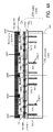
- FIG. 1 shows an exemplary package of multiple ICs 110 connected to each other and/or other circuits (not shown) through interposers (“ITP”) 120 . 1 and 120 . 2 and wiring substrate 130 .
- ITP interposers
- ICs 110 are attached to the interposers in a flip-chip manner, i.e. the ICs' bottom contact pads 110 C are attached to top contact pads 120 C.T of respective interposers 120 . 1 , 120 . 2 by connections 134 .
- Connections 134 can be formed by solder or solder composite, adhesive, diffusion bonding, or some other means.
- Interposers 120 (i.e. 120 . 1 and 120 . 2 ) have bottom contact pads 120 C.B attached to the wiring substrate's top contact pads 130 C by connections 138 (e.g. solder).
- Each interposer 120 (i.e. 120 . 1 and 120 . 2 ) includes conductive lines 120 L interconnecting its contact pads 120 C.T and 120 C.B in a desired pattern in order to connect the respective ICs 110 to each other and to wiring substrate 130 .
- Wiring substrate 130 has conductive lines 130 L interconnecting the wiring substrate's contact pads 130 C and hence interconnecting the ICs 110 located on the same or different interposers 120 .
- wiring substrates 130 are made of inexpensive, possibly non-semiconductor material (e.g. organic or ceramic) processed by inexpensive techniques (e.g. printing) to form the conductive lines 130 L.
- ICs 110 are manufactured by high precision but more expensive semiconductor technology allowing the ICs to be small and have high performance. As a result, the ICs' contact pads 110 C can be spaced closer to each other (at a lower pitch) than the wiring substrate's contact pads 130 C. Consequently, the ICs cannot be flip-chip attached to the wiring substrate.
- Interposers 120 “redistribute” the contact pads: the interposers 120 can be manufactured by high precision technology, with the top contact pads 120 C.T matching the ICs' contact pads 110 C but with the bottom contact pads 120 C.B matching the wiring substrate.
- interposers 120 absorb and dissipate some of the heat generated by the ICs and thus reduce thermo-mechanical stresses (mechanical stresses resulting from thermal expansion). Also, if the interposers' coefficients of thermal expansion (CTE) are intermediate between the wiring substrate and the ICs, or are close to the ICs, then the IC-to-interposer connections 134 experience less thermo-mechanical stress.
- the connections 138 between the interposers and the wiring substrate may experience higher stresses due to the CTE mismatch between the interposers and the wiring substrate, but connections 138 can be made larger due to their high pitch, and therefore can be sturdy and reliable.
- Each IC or interposer is typically manufactured in a large wafer format with other ICs or interposers, and the wafer is diced (singulated) into individual ICs or interposers (which are called die or chips).
- the ICs 110 , interposers 120 , and wiring substrate 130 can be attached to each other after dicing; see e.g. U.S. Pat. No. 8,138,015 B2 issued Mar. 20, 2012 to Joseph et al.
- reliable attachment of tiny, fragile ICs 110 to interposers is difficult.
- wafer-level packaging is used, with some of the ICs or interposers being attached to each other before singulation and possibly even before the end of wafer processing; for instance, ICs 110 can be attached to interposers 120 before singulation of at least some of wafers.
- some of the wafers can be initially thick for increased reliability, and can be thinned late in the manufacturing process; in such cases, some of the IC and interposer attachments can be performed before wafer thinning.
- FIG. 2A One example is shown in FIG. 2A : the interposer wafer 120 W has not yet been singulated, but will be singulated along the lines 140 to form multiple interposers of the type of interposer 120 . 1 of FIG. 1 .
- the IC wafers have been singulated, and ICs 110 have been attached to interposer wafer 120 W.
- the interposers' bottom contact pads 120 C.B have not yet been formed, and the interposer wafer 120 W is thicker (and hence stronger) than its final size; the ICs have been attached before thinning of wafer 120 W.
- Interposers 120 . 2 are fabricated in another wafer (not shown), possibly using the same or different wafer-level packaging techniques.
- the interposer wafer of FIG. 2A is based on a substrate 120 S (e.g. silicon or glass or other material with a CTE similar to the ICs).
- the interposer's conductive lines 120 L include vertical vias 120 LV going down into substrate 120 S, and include other lines 120 LH at the top of the wafer.
- Lines 120 LH are electrically insulated from each other and from substrate 120 S by dielectric 210 D; lines 120 LH and dielectric 210 D form a “redistribution layer” (RDL) 210 used to redistribute the contact pads as described above.
- RDL redistribution layer
- Interposer wafer 120 W is thinned from the bottom to expose the bottom ends of vias 120 LV; the bottom ends will be used as contact pads 120 C.B.
- wafer 120 W and substrate 120 S become thin and fragile, easy to damage during or after thinning.
- thinned wafer 120 W can be warped, which complicates further processing including interposer attachment to wiring substrate 130 . Therefore, before thinning, wafer 120 W with ICs 110 attached at the top, can be strengthened by mold compound 310 ( FIG. 2B ) and carrier 320 .
- Mold compound 310 is typically an organic polymeric material with fillers (e.g. silica).
- Carrier 320 can be a glass or silicon wafer, attached by adhesive 330 .
- interposer substrate 120 S is then thinned from the bottom, e.g. by mechanical and/or chemical processes, to expose the vias 120 LV.
- the bottom ends of vias 120 LV become contact pads 120 C.B. Additional metal (e.g. solder) can be deposited on these bottom ends if needed.
- carrier 320 is debonded or ground away, the interposer wafer is singulated along lines 140 together with mold 310 , and individual interposers 120 . 1 , with ICs 110 C on top, are attached to the same or different wiring substrates 130 as in FIG. 1 .
- mold compounds contribute to warpage because their CTEs are typically higher than for interposer wafers.
- the warpage progressively increases as the interposer wafer is thinned with mold compound on top. This complicates the process required to uniformly expose the vias 120 LV during thinning.
- the increased warpage also complicates attaching the singulated substrate 120 S to the wiring substrates 130 .
- a mold compound was deposited; the mold compound filled the gaps between the die and had a planar top surface, being 350 ⁇ m thick over the die.
- the warpage increased to about 1200 ⁇ m.
- the top surface was lapped to remove the mold compound over the die and reduce the die thickness by 20 ⁇ m; the warpage was reduced, but remained slightly under 1000 ⁇ m.
- the bottom wafer was ground to 100 ⁇ m thickness. The warpage decreased but stayed above 500 ⁇ m.
- Some embodiments of the present invention reduce the wafer warpage by forming one or more gap regions, e.g. air gaps, between the mold compound and the interposer wafer.
- the mold compound is replaced by other materials that may or may not be deposited by techniques other than molding.
- the mold compound or other materials form a layer that stabilizes (strengthens) the wafer due to adhesion to ICs 110 , possibly without contacting the wafer or contacting the wafer only in limited areas (due to the gap regions).
- the gap regions reduce the thermo-mechanical forces exerted by the stabilization layer on the interposer wafer, and thus reduce the warpage.
- the stabilization layer can be formed by non-molding techniques, e.g. lamination. Suitable laminates include materials conventionally used as dry film resists. They adhere well to the top of ICs 110 , and are easy to remove (e.g. by laser ablation or grinding), so no adhesive is needed between the stabilization layer and the ICs 110 . Further, in some embodiments, the stabilization layer can be left in the final structure.
- the stabilization layer includes a bottom sub-layer of porous material (e.g. aerogel or some other type of foam) with low elastic modulus in the horizontal direction (i.e. the direction parallel to interposer wafer 120 W).
- the low horizontal modulus limits the stress exerted by the stabilization layer on the interposer wafer.
- the stabilization layer has a high flexural modulus and hence high flexural strength, to resist warpage and strengthen the structure for further processing. These properties—high flexural modulus and low horizontal elastic modulus—are obtained in some foams.
- the stabilization layer may include one or more higher sub-layers with higher flexural moduli, e.g. non-porous sub-layers or sub-layers made of a foam having a lower porosity than the bottom sub-layer, to further strengthen the structure.
- the stabilization layer or at least its bottom sub-layer may or may not at least partially remain in the final structure.
- the stabilization layer is sufficiently strong to allow omission of carrier 320 .
- carrier bonding and debonding create reliability problems because on the one hand the adhesive 330 must be strong enough to withstand substrate thinning and subsequent processing of the bottom ends of vias 120 LV, and on the other hand the adhesive 330 must be easily deactivated in the debonding process. Further, the bonding and debonding operations may have to be performed at low temperatures to avoid damage to the ICs and the interposer, and this further limits the choice of adhesives 330 . If the carrier is attached by a permanent bond and then ground away, the grinding process also creates reliability problems. Carrier elimination is therefore desirable.
- the stabilization layer itself may or may not change the warpage, possibly reducing or increasing the warpage in at least one area.
- packaging techniques described above are not limited to interposers or to the IC/interposer structures of the type shown in FIG. 1 , and further the invention is not limited to the packaging techniques described above or any other features described above or below except as defined by the appended claims.
- FIGS. 1, 2A, 2B, 3 illustrate vertical cross sections of semiconductor package structures according to prior art.
- FIG. 4A illustrates a vertical cross section of a semiconductor package structure according to some embodiments of the present invention.
- FIG. 4B illustrates a top view of a semiconductor package structure according to some embodiments of the present invention.
- FIG. 5 is a flowchart of a packaging process according to some embodiments of the present invention.
- FIGS. 6, 7, 8, 9, 10, 11, 12, 13, 14 illustrate vertical cross sections of semiconductor package structures according to some embodiments of the present invention.
- FIG. 4A shows a stabilization layer 404 which can be formed, for example, in the structure of FIG. 2A or 2B or 3 , possibly before, in the middle, or after thinning of the interposer wafer.
- the stabilization layer is formed before the wafer thinning, and will protect the ICs from wafer thinning byproducts during the thinning operation.
- FIG. 4A also shows some optional, conventional features such as underfill 410 , possibly filled organic polymeric material. Underfills are well-known adhesives that bind ICs to interposers or wiring substrates (e.g. organic substrates) to strengthen the connections 134 . The underfill is optional.
- dielectric 430 electrically insulating the vias 120 LV from interposer substrate 120 S.
- Dielectric 430 is usually absent if interposer substrate 120 S is itself dielectric (e.g. glass).
- Stabilizing layer 404 covers the structure and adheres to ICs 110 without additional adhesive.
- Layer 404 is separated from the interposer wafer 120 W by a gap region (air gap) 450 at the interposer areas not covered by the ICs.
- FIG. 4B shows the top view of the structure with stabilization layer 404 removed.
- the markings A-A denote the vertical cross sectional plane of FIG. 4A .
- air gap 450 extends throughout the area not occupied by ICs 110 . In other embodiments, the air gap may be more restricted.
- stabilization layer 404 contacts the interposer wafer 120 W at the wafer edges, possibly along the entire wafer edge 404 E, so the air gap does not extend to the edges.
- the air gap is absent in a limited area 454 in the middle of wafer 120 W, between the ICs 110 or over one or more of the ICs, where the stabilization layer 404 adheres to the interposer wafer 120 W (or underfill 410 if present) and thus strengthens the wafer without a significant warpage effect.
- the stabilization layer itself may or may not change the warpage, possibly reducing or increasing the warpage in at least one area (possibly the whole area of the structure).
- Other geometries of air gap 450 are possible.
- Stabilization layer 404 can be a continuous layer covering the entire interposer wafer 120 W, or may have through-holes at any desired places, e.g. over one or more ICs 410 or between the ICs. Further, stabilization layer 404 may consist of a number of disconnected pieces. Such features (holes and/or disconnected pieces) may be provided to reduce the wafer warpage or for other purposes.
- Stabilization layer 404 is a material which can be formed in the structure at suitable temperatures (e.g. below 400° C. for some structures) so as to have strong adhesion to all or some of the top surfaces of ICs 110 .
- one or more of the ICs can be replaced by microelectronic packages (MPs), e.g. multichip modules (MCMs), and then the stabilization layer has strong adhesion to all or some of the IC or MP top surfaces.
- the ICs' or MPs' top surfaces can be organic and/or inorganic materials, and can have any electrical properties including conductor (e.g. a metal heat sink), semiconductor (e.g. silicon), or dielectric (e.g. silicon dioxide, silicon nitride, silicon oxynitride, polyimide, or other types commonly used as IC passivation layers, or ceramic or other materials).
- stabilization layer 404 may have downward protrusions 404 P over all or part of the wafer area not covered by the ICs 110 .
- Downward protrusions 404 P narrow the gap 450 but they strengthen the structure, possibly reducing warpage.
- protrusions 404 P have good adhesion to the IC or MP sidewalls, with possibly the same adhesion strength as between layer 404 and the respective IC or MP top surfaces.
- stabilization layer 404 is a material commonly used as dry film resist, or a similar non-photoimageable material (similar in the sense that it can be formed by substantially the same techniques and have substantially the same warpage reduction properties).
- stabilization layer 404 is laminated onto the ICs (or MPs) at step 480 .
- the resulting structure is shown in FIG. 6 .
- Stabilization layer 404 does not have protrusions 404 P at this stage.
- Layer 404 covers the areas between the ICs but is separated by a gap region 450 from the interposer wafer (the gap region can be filled by air or some other gas; the gas may or may not be at vacuum).
- Stabilization layer 404 may or may not be a flat sheet at this stage.
- the layer 404 may be recessed between the ICs 110 at least in wider areas between the ICs, and may physically contact the underfill 410 or wafer 120 W along the wafer edge 404 E.
- layer 404 is softened to flow down and form downward protrusions 404 P ( FIG. 4A ).
- layer 404 is cured if needed to increase its strength (e.g. increase its horizontal elastic modulus and flexural modulus).
- layer 404 is softened by heat. This is appropriate for example if layer 404 is thermoplastic at this stage—layer 404 can be organic or inorganic thermoplastic material. In some of these embodiments, layer 404 becomes thermosetting at higher temperatures of the curing step 490 .
- layer 404 can be patterned to form through holes or disconnected pieces as mentioned above.
- the patterning can be done at any suitable stage before or after lamination, before or after step 484 , and before or after step 490 , by photolithography (if layer 404 is photoimageable at the patterning stage then no additional photoresist is used in some embodiments), laser ablation, or any other suitable means.
- An exemplary starting material is a flat epoxy sheet known as SUEX TDFS (Thick Dry Film Sheet) available from DJ DevCorp of Massachusetts, United States.
- the main SUEX ingredient is Bisphenol A Novolac epoxy.
- the epoxy In its viscous form known as Su-8, the epoxy is dissolved in an organic solvent (primarily gamma-butyrolactone (GBL) or cyclopentanone, depending on the formulation) and up to 10 wt % of mixed Triarylsulfonium/hexafluoroantimonate salt as the photoacid generator.
- GBL gamma-butyrolactone
- cyclopentanone cyclopentanone
- the solvent amount In the dry form (SUEX), the solvent amount is less than 1 wt %.
- Fully cured SUEX tape obtained at step 490 may have a horizontal elastic modulus of 3.9 GPa and tensile strength of 86 MPa (both measured by ASTM D3379-75, Dage tensile pull).
- the initial thickness of SUEX sheet 404 (before step 480 ) can be 30 to 2000 ⁇ m, but this is not limiting.
- the tape is laminated in vacuum at an ambient temperature of 25 to 150° C. and ambient pressure of 10 to 30 mTorr for 2 to 60 minutes.
- the SUEX material is thermoplastic at this stage, so it flows down into the air gap to form the downward protrusions 404 P ( FIG. 4A ) around each IC 110 .
- the height hp of each protrusion 404 P is 10 to 90% of the thickness of the IC 110 .
- the protrusion height may vary over the wafer 120 W depending on the lateral distance between the adjacent ICs 110 and on the materials of the sidewalls of the adjacent ICs (capillary effect).
- the height ha of gap 450 depends on the height of ICs 110 , and is at least 1 ⁇ m in some embodiments except at the wafer edge 404 E.
- SUEX layer 404 is cured at step 490 .
- the SUEX material becomes thermosetting through cross-linking due to epoxy polymerization.
- FIG. 5 processing examples include other epoxies, not necessarily photoimageable. These materials and other materials described herein may have additives (e.g. flame retardants) that do not materially affect their warpage reduction function.
- additives e.g. flame retardants
- top and/or bottom surfaces of stabilization layer 404 may be non-planar at any stage and may have any topology.
- protrusions 404 P may reach the interposer wafer 120 W in some areas to close the gap 450 .
- the reach of protrusions 404 P is controlled by localized heat, e.g. UV radiation: more heat is supplied at those locations where longer protrusions 404 P are desired.
- Protrusions 404 P may also be formed before lamination of layer 404 over the ICs.
- a possible process is embossing ( FIG. 7 ) using a suitable stamp 610 , possibly glass, metal, organic polymer, or some other material.
- the stamp is pressed into a possibly flat layer 404 to form cavities 620 corresponding to the topology of ICs 110 .
- the stamped layer 404 is then cured if needed, and placed over the ICs as in FIG. 4A .
- layer 404 has good adhesion to the IC/MP materials mentioned above, so no additional adhesive is needed.
- the adhesion is good both at the top surfaces and the sidewalls of the ICs or MPs.
- stabilization layer 404 can be further cured if needed, and can be patterned either before or after the lamination (e.g. during the embossing process).
- layer 404 is softened.
- the softening can be done by heat if, for example, layer 404 is thermoplastic.
- SUEX and some other materials can be softened by UV light transmitted from above the layer 404 , or from below through the stamp 610 if the stamp is transparent to the UV radiation (the dose and other parameters are adjusted in accordance with the stamp's transmissivity).
- the layer 404 is cured before removing the stamp 610 . After the SUEX layer 404 is placed on the ICs, layer 404 is further cured.
- Embossing can also be performed on other materials.
- protrusions 404 P before lamination of stabilization layer 404 .
- Examples include chemical etches, laser ablation, printing of protrusions 404 P (or possibly of the entire stabilization layer 404 ), and molding.
- stabilization layer 404 can be strengthened by a carrier 320 ( FIG. 8 ) attached to the top surface of layer 404 by adhesive 330 as in FIG. 2B or 3 .
- the carrier and the adhesive can be any materials consistent with the warpage reduction and other objectives, e.g. improved thermal conductivity for heat dissipation during manufacturing.
- stabilization layer 404 can be thinned before carrier attachment.
- the thinning process may or may not expose one or more (possibly all) ICs or MPs 110 from the top.
- the thinning process can be mechanical (lapping), chemical, or some other way. Part or all of the thinning process can be performed before full curing of layer 404 (i.e. before step 490 ) by chemical, mechanical, chemical-mechanical, and/or some other process(es).
- the interposer wafer 120 W is thinned from the bottom by thinning the interposer substrate 120 S to expose the vias 120 LV (if dielectric 430 is present then it is removed at the bottom). This thinning can be done by conventional processes, using mechanical, chemical, chemical/mechanical, and/or other techniques.
- the bottom ends of vias 120 LV provide the interposer bottom contact pads 120 C.B in the example of FIG. 8 .
- additional circuitry e.g. RDL, similar to RDL 210
- RDL is formed on the bottom surface of interposer substrate 120 S to provide the bottom contact pads 120 C.B and connect these pads to the bottom ends of vias 120 LV.
- Additional layers 138 can be provided on bottom contact pads 120 C.B as needed.
- the interposer wafer 120 W is singulated along the lines 140 .
- Stabilization layer 404 is singulated at the same time.
- Carrier 320 if present, can be debonded before singulation.
- FIG. 9 shows a single die obtained in the singulation process (this die contains two die 110 and one interposer die 120 ).
- a heat sink (not shown) can be attached at the top of the structure (e.g. to the exposed IC surfaces).
- the heat sink has one or more cavities; the ICs 110 are in the cavities; the heat sink is attached to the interposer 120 around the ICs; the cavities contain thermal interface material (TIM, e.g. gel (possibly filled) or some other type) that contacts the ICs and the heat sink and provides a thermal path therebetween.
- TIM's thermal conductivity is higher than air.
- FIGS. 10-12 illustrate another approach for warpage reduction, using a porous stabilization sub-layer 404 . 1 .
- the underlying structure is as in FIG. 4A , with ICs 110 , interposer wafer 120 W, and underfill 410 .
- Porous sub-layer 404 . 1 is formed over the structure, using any suitable techniques. Due to its porosity, layer 404 . 1 has a low horizontal elastic modulus, possibly 4 GPa or below, in order to reduce the thermo-mechanical stress on wafer 120 W.
- layer 404 . 1 has a high flexural modulus to strengthen the structure; the flexural modulus can be higher than the horizontal modulus.
- the horizontal modulus can be 500 MPa or less, possibly 100 MPa or less, while the flexural modulus under the three-point test can be higher.
- the appropriate moduli depend on the CTE mismatches and the final strength of the structure; for example, if the thinned interposer wafer is strong despite thinning, and/or the ICs 110 are densely positioned to strengthened the structure, than a lower flexural modulus and a higher horizontal modulus may be suitable.
- the porosity of layer 404 . 1 can be from 1% to 92% or higher.
- the average pore size can be 2 to 50 ⁇ m, and other sizes below or above this range are possible.
- the pores can be partially or completely filled with a thermal interface material (TIM); as used herein, TIM is any material having a thermal conductivity above the material of layer 404 . 1 .
- Example TIMs are gels (possibly filled) and powders.
- Layer 404 . 2 may have the same structure and properties except for its higher horizontal and/or flexural modulus (TIM can be used as any material having a higher thermal conductivity than the material of layer 404 . 2 ).
- Layer 404 . 2 can be absent.
- TIM is optional, and if used then it can be limited to parts of layer 404 . 1 .
- layer 404 . 1 may have areas of different thermal conductivity. Lower thermal conductivity may be provided between those ICs 110 which should be thermally isolated from each other. For example, the pores can be filled with air in those areas.
- a stiffer layer 404 . 2 (i.e. with a higher horizontal and/or flexural modulus) is formed over layer 404 . 1 .
- the resulting layer 404 i.e. combination of layers 404 . 1 and 404 . 2
- stiffer layer 404 . 2 acts as sealing layer to prevent the debris of the interposer thinning process from getting into porous layer 404 . 1 .
- Layer 404 . 1 and/or 404 . 2 can be patterned with through holes or discontinuous pieces as described above for FIG. 4A .
- Subsequent processing can be as described in connection with FIGS. 8-9 . Any variations described above can be used with the porous layers as appropriate, including different types of interposer/IC structures and non-interposer structures.
- Exemplary materials for layer 404 . 1 include foams (i.e. porous materials with gas filled pores), e.g. organic polymeric foams.
- Suitable foams include aerogels, e.g. polyimide aerogels.
- Suitable polyimide aerogels are described, for example, by NASA (National Aeronautics and Space Administration), United States of America, in a data sheet “NASA's Glenn Research Center's Mechanically Strong, Flexible Polyimide Aerogels”, Oct. 16, 2012 (2 pages), incorporated herein by reference. See also the following U.S. pre-grant patent publications incorporated herein by reference: 2015/0141544 A1 (May 21, 2015; inventors: Meador et al.); 2015/0076987 A1 (Mar.
- NASA's polyimide aerogels can withstand 300° C. temperatures, making them suitable for many wafer thinning processes.
- Their elastic modulus can be 1 to 100 MPa.
- Their porosity can be varied, and can exceed 90%, ensuring a correspondingly low horizontal elastic modulus.
- the polyimide aerogel film can have a high flexural modulus.
- An aerogel is obtained by supercritical drying of a gel.
- Layer 404 . 1 can be shaped by embossing (such as described above in connection with FIG.
- polyimide aerogel layer 404 . 1 has a planar top surface overlying the tallest IC 110 and the areas not covered by the ICs.
- the average pore size is 2 to 50 ⁇ m in some embodiments.
- Such aerogels have a low thermal conductivity (e.g. 14 mW/m-K according to the NASA reference), and can be used to thermally isolate the adjacent ICs 110 from each other.
- TIM can be provided in those areas where high thermal conductivity is desired.
- suitable materials include polyurethane foams. Still other materials can be suitable.
- layer 404 . 1 can be stiffened by an additional layer in the pores.
- the additional layer can be electrolessly plated nickel, e.g. to a thickness of 5 ⁇ m or below (higher thickness can also be used; suitable thickness depends on many factors including the desired additional stiffness to be provided by the additional material).
- sub-layer 404 . 1 can be patterned with holes, possibly through-holes, which can be filled by the stiffer layer 404 . 2 to stiffen the structure.
- layer 404 . 1 is absent at the edges of the structure where it is replaced by downward protruding portions of layer 404 . 2 ( FIG. 11 ).
- Layer 404 . 2 can be any suitable material having a higher horizontal and/or flexural modulus than layer 404 . 1 .
- Suitable materials for layer 404 . 2 include mold compounds (as in FIG. 3 ), or the same types of materials as described above for layer 404 . 1 .
- layers 404 . 1 and 404 . 2 are the same material except that the layer 404 . 2 has lower porosity and hence higher horizontal and flexural moduli.
- the porosities of layers 404 . 1 and 404 . 2 are respectively 90% and 1%.
- layer 404 . 2 has a planar top surface and is 1 to 50 ⁇ m thick above the layer 404 . 1 . This is not limiting.
- FIG. 12 shows a single die after singulation of the interposer wafer 120 W and of the underfill and stabilization layers 410 , 440 . 1 , 440 . 2 .
- This die contains two die 110 and one interposer die 120 .
- layer 404 . 1 has graded porosity—the porosity gradually decreases from the bottom to the top.
- Layer 404 . 2 may be absent.
- ICs can be replaced by microelectronic packages.
- any components including discrete components, can be present in addition to ICs.
- Exemplary components are wires 1310 ( FIG. 13 ) attached to some of contact pads 120 C.T before deposition of layers 404 . 1 and 404 . 2 .
- Wires 1310 may or may not be vertical. They can be bonded to contact pads 120 C.T by ultrasound bonding, like the BVA wires (Bond Via Array), or can be formed photolithographically or possibly by some other techniques; see InvensasTM High Performance BVA PoP package for Mobile Systems , May 2013 by Invensas Corporation of San Jose, Calif., incorporated herein by reference; see also U.S. Pat.
- Wires 1310 can be connected to other components (e.g. IC 110 ′ in FIG. 14 ) to form a vertically integrated package.
- FIG. 14 shows the structure after dicing.
- Wires 1310 are attached to contact pads 110 C of IC 110 ′ by solder or solder composite 1410 .
- IC 110 ′ overlaps the lower IC 110 .
- Other connections and packages are also possible.
- interposer wafer 120 W can be replaced by a reconstituted wafer, a glass or polymeric panel (such as used in liquid crystal displays for example), a sacrificial substrate later removed (e.g. a sapphire substrate used for sensor fabrication), or some other type of structure.
- a fabrication process comprising:
- first modules each of which comprises circuitry comprising one or more contact pads
- a first module can be an IC 110 or MCM or some other package or packaging component, e.g. a wiring substrate
- a first structure e.g. interposer wafer 120 W, possibly with underfill 410 ) comprising circuitry comprising one or more contact pads at a top side of the first structure;
- a gap region is any region filled with gas, at any pressure, possibly at vacuum.
- each first module has a sidewall surface exposed in the one or more gap regions.
- each first module comprises a semiconductor integrated circuit.
- a structure comprising:
- one or more first modules each of which comprises circuitry comprising one or more contact pads
- a first structure comprising circuitry comprising one or more contact pads at a top side of the first structure
- first layer over the first structure, the first layer adhering to the one or more first modules and overlying one or more areas of a top surface of the first structure which are not covered by the one or more first modules, the first layer being separated from the one or more areas by one or more gap regions underlying the first layer.
- each first module has a sidewall surface exposed in the one or more gap regions.
- each first module comprises a semiconductor integrated circuit.
- a fabrication process comprising:
- one or more first modules each of which comprises circuitry comprising one or more contact pads
- a first structure comprising circuitry comprising one or more contact pads at a top side of the first structure
- the one or more first modules are attached to the top side of the first structure, wherein the one or more contact pads of the one or more first modules being attached to the one or more contact pads of the first structure;
- first layer e.g. 404 . 1
- first layer adhering to the one or more first modules, the first layer being porous and extending substantially along a first plane, the first layer having a lower elastic modulus along the first plane than a flexural modulus in a direction perpendicular to the first plane.
- a structure comprising:
- one or more first modules each of which comprises circuitry comprising one or more contact pads
- a first structure comprising circuitry comprising one or more contact pads at a top side of the first structure
- the one or more first modules are attached to the top side of the first structure, the one or more contact pads of the one or more first modules being attached to the one or more contact pads of the first structure;
- first layer over the first structure, the first layer adhering to the one or more first modules, the first layer being porous and extending substantially along a first plane, the first layer having a higher elastic modulus along the first plane than a flexural modulus in a direction perpendicular to the first plane.
Abstract
Description
Claims (19)
Priority Applications (3)
| Application Number | Priority Date | Filing Date | Title |
|---|---|---|---|
| PCT/US2015/050026 WO2016044179A2 (en) | 2014-09-15 | 2015-09-14 | Electronic structures strengthened by porous and non-porous layers, and methods of fabrication |
| US14/852,855 US9799626B2 (en) | 2014-09-15 | 2015-09-14 | Semiconductor packages and other circuit modules with porous and non-porous stabilizing layers |
| TW104130552A TWI590331B (en) | 2014-09-15 | 2015-09-15 | Electronic structures strengthened by porous and non-porous layers, and methods of fabrication |
Applications Claiming Priority (2)
| Application Number | Priority Date | Filing Date | Title |
|---|---|---|---|
| US201462050728P | 2014-09-15 | 2014-09-15 | |
| US14/852,855 US9799626B2 (en) | 2014-09-15 | 2015-09-14 | Semiconductor packages and other circuit modules with porous and non-porous stabilizing layers |
Publications (2)
| Publication Number | Publication Date |
|---|---|
| US20160079138A1 US20160079138A1 (en) | 2016-03-17 |
| US9799626B2 true US9799626B2 (en) | 2017-10-24 |
Family
ID=55455472
Family Applications (1)
| Application Number | Title | Priority Date | Filing Date |
|---|---|---|---|
| US14/852,855 Active US9799626B2 (en) | 2014-09-15 | 2015-09-14 | Semiconductor packages and other circuit modules with porous and non-porous stabilizing layers |
Country Status (3)
| Country | Link |
|---|---|
| US (1) | US9799626B2 (en) |
| TW (1) | TWI590331B (en) |
| WO (1) | WO2016044179A2 (en) |
Families Citing this family (5)
| Publication number | Priority date | Publication date | Assignee | Title |
|---|---|---|---|---|
| CN111211059B (en) * | 2018-11-22 | 2023-07-04 | 矽品精密工业股份有限公司 | Electronic package, manufacturing method thereof and heat dissipation part |
| US11315860B2 (en) * | 2019-10-17 | 2022-04-26 | Taiwan Semiconductor Manufacturing Company, Ltd. | Semiconductor package and manufacturing process thereof |
| EP3944290A1 (en) * | 2020-07-21 | 2022-01-26 | Infineon Technologies Austria AG | Chip-substrate composite semiconductor device |
| CN113782457B (en) * | 2021-08-20 | 2023-11-21 | 长江存储科技有限责任公司 | Method for manufacturing bonding wafer and wafer bonding machine |
| CN117038599A (en) * | 2023-10-07 | 2023-11-10 | 之江实验室 | Chip packaging structure and packaging method |
Citations (30)
| Publication number | Priority date | Publication date | Assignee | Title |
|---|---|---|---|---|
| EP0512401A2 (en) | 1991-05-03 | 1992-11-11 | International Business Machines Corporation | Low dielectric constant composite laminates filled with molecularly porous aerogels |
| US5379186A (en) * | 1993-07-06 | 1995-01-03 | Motorola, Inc. | Encapsulated electronic component having a heat diffusing layer |
| EP0962974A2 (en) | 1998-05-28 | 1999-12-08 | Hitachi, Ltd. | Semiconductor device |
| US6455785B1 (en) | 1998-10-28 | 2002-09-24 | International Business Machines Corporation | Bump connection with stacked metal balls |
| US20050224829A1 (en) * | 2004-04-06 | 2005-10-13 | Negley Gerald H | Light-emitting devices having multiple encapsulation layers with at least one of the encapsulation layers including nanoparticles and methods of forming the same |
| US20070045798A1 (en) * | 2005-08-01 | 2007-03-01 | Nec Electronics Corporation | Semiconductor package featuring metal lid member |
| US20070139892A1 (en) * | 2005-12-20 | 2007-06-21 | Fujitsu Limited | Semiconductor device |
| US20090261484A1 (en) * | 2006-12-20 | 2009-10-22 | Naoki Kanagawa | Liquid resin composition, semi-conductor device, and process of fabricating the same |
| US7816183B2 (en) | 2006-12-27 | 2010-10-19 | Nec Electronics Corporation | Method of making a multi-layered semiconductor device |
| US20110272785A1 (en) * | 2009-01-20 | 2011-11-10 | Teik Tiong Toong | Ic package with capacitors disposed on an interposal layer |
| US8129849B1 (en) * | 2006-05-24 | 2012-03-06 | Amkor Technology, Inc. | Method of making semiconductor package with adhering portion |
| US8138015B2 (en) | 2008-04-28 | 2012-03-20 | International Business Machines Corporation | Interconnection in multi-chip with interposers and bridges |
| US20130082399A1 (en) | 2011-10-04 | 2013-04-04 | Won-keun Kim | Semiconductor package and method of manufacturing the same |
| US8426961B2 (en) * | 2010-06-25 | 2013-04-23 | Taiwan Semiconductor Manufacturing Company, Ltd. | Embedded 3D interposer structure |
| US20130285259A1 (en) | 2012-04-30 | 2013-10-31 | Caleb C. Han | Method and system for wafer and strip level batch die attach assembly |
| US8618659B2 (en) | 2011-05-03 | 2013-12-31 | Tessera, Inc. | Package-on-package assembly with wire bonds to encapsulation surface |
| US20140036454A1 (en) | 2012-08-03 | 2014-02-06 | Invensas Corporation | Bva interposer |
| US20140077352A1 (en) * | 2012-09-14 | 2014-03-20 | George R. Leal | Matrix Lid Heatspreader for Flip Chip Package |
| US20140110049A1 (en) | 2012-10-19 | 2014-04-24 | The Hong Kong University Of Science And Technology | Three Dimensional Interconnected Porous Graphene-Based Thermal Interface Materials |
| US20140124955A1 (en) | 2012-11-08 | 2014-05-08 | Taiwan Semiconductor Manufacturing | Package-on-package structure including a thermal isolation material and method of forming the same |
| US8822269B2 (en) * | 2005-04-19 | 2014-09-02 | Renesas Electronics Corporation | Semiconductor device and method of manufacturing the same |
| US20140272358A1 (en) | 2013-03-14 | 2014-09-18 | Ohio Aerospace Institute | Porous cross-linked polyimide-urea networks |
| US8841759B2 (en) | 2006-12-23 | 2014-09-23 | Lg Innotek Co., Ltd. | Semiconductor package and manufacturing method thereof |
| US8969132B2 (en) | 2010-09-20 | 2015-03-03 | Nuvotronics, Llc | Device package and methods for the fabrication thereof |
| US20150076987A1 (en) | 2013-05-24 | 2015-03-19 | National Institute Of Aerospace Associates | Robust, Flexible and Lightweight Dielectric Barrier Discharge Actuators Using Nanofoams/Aerogels |
| US9012269B2 (en) | 2008-12-30 | 2015-04-21 | Stmicroelectronics Pte Ltd. | Reducing warpage for fan-out wafer level packaging |
| US20150141544A1 (en) | 2012-02-03 | 2015-05-21 | U.S. Government as represented by the Administrator of the National Aeronautics and Spac | Porous cross-linked polyimide networks |
| WO2015102838A1 (en) | 2013-12-31 | 2015-07-09 | Halliburton Energy Services, Inc. | Methods and apparatus for evaluating downhole conditions with rfid mems sensors |
| US20150364392A1 (en) * | 2013-09-03 | 2015-12-17 | Renesas Electronics Corporation | Semiconductor device with covering member that partially covers wiring substrate |
| US9252127B1 (en) * | 2014-07-10 | 2016-02-02 | Invensas Corporation | Microelectronic assemblies with integrated circuits and interposers with cavities, and methods of manufacture |
-
2015
- 2015-09-14 WO PCT/US2015/050026 patent/WO2016044179A2/en active Application Filing
- 2015-09-14 US US14/852,855 patent/US9799626B2/en active Active
- 2015-09-15 TW TW104130552A patent/TWI590331B/en active
Patent Citations (30)
| Publication number | Priority date | Publication date | Assignee | Title |
|---|---|---|---|---|
| EP0512401A2 (en) | 1991-05-03 | 1992-11-11 | International Business Machines Corporation | Low dielectric constant composite laminates filled with molecularly porous aerogels |
| US5379186A (en) * | 1993-07-06 | 1995-01-03 | Motorola, Inc. | Encapsulated electronic component having a heat diffusing layer |
| EP0962974A2 (en) | 1998-05-28 | 1999-12-08 | Hitachi, Ltd. | Semiconductor device |
| US6455785B1 (en) | 1998-10-28 | 2002-09-24 | International Business Machines Corporation | Bump connection with stacked metal balls |
| US20050224829A1 (en) * | 2004-04-06 | 2005-10-13 | Negley Gerald H | Light-emitting devices having multiple encapsulation layers with at least one of the encapsulation layers including nanoparticles and methods of forming the same |
| US8822269B2 (en) * | 2005-04-19 | 2014-09-02 | Renesas Electronics Corporation | Semiconductor device and method of manufacturing the same |
| US20070045798A1 (en) * | 2005-08-01 | 2007-03-01 | Nec Electronics Corporation | Semiconductor package featuring metal lid member |
| US20070139892A1 (en) * | 2005-12-20 | 2007-06-21 | Fujitsu Limited | Semiconductor device |
| US8129849B1 (en) * | 2006-05-24 | 2012-03-06 | Amkor Technology, Inc. | Method of making semiconductor package with adhering portion |
| US20090261484A1 (en) * | 2006-12-20 | 2009-10-22 | Naoki Kanagawa | Liquid resin composition, semi-conductor device, and process of fabricating the same |
| US8841759B2 (en) | 2006-12-23 | 2014-09-23 | Lg Innotek Co., Ltd. | Semiconductor package and manufacturing method thereof |
| US7816183B2 (en) | 2006-12-27 | 2010-10-19 | Nec Electronics Corporation | Method of making a multi-layered semiconductor device |
| US8138015B2 (en) | 2008-04-28 | 2012-03-20 | International Business Machines Corporation | Interconnection in multi-chip with interposers and bridges |
| US9012269B2 (en) | 2008-12-30 | 2015-04-21 | Stmicroelectronics Pte Ltd. | Reducing warpage for fan-out wafer level packaging |
| US20110272785A1 (en) * | 2009-01-20 | 2011-11-10 | Teik Tiong Toong | Ic package with capacitors disposed on an interposal layer |
| US8426961B2 (en) * | 2010-06-25 | 2013-04-23 | Taiwan Semiconductor Manufacturing Company, Ltd. | Embedded 3D interposer structure |
| US8969132B2 (en) | 2010-09-20 | 2015-03-03 | Nuvotronics, Llc | Device package and methods for the fabrication thereof |
| US8618659B2 (en) | 2011-05-03 | 2013-12-31 | Tessera, Inc. | Package-on-package assembly with wire bonds to encapsulation surface |
| US20130082399A1 (en) | 2011-10-04 | 2013-04-04 | Won-keun Kim | Semiconductor package and method of manufacturing the same |
| US20150141544A1 (en) | 2012-02-03 | 2015-05-21 | U.S. Government as represented by the Administrator of the National Aeronautics and Spac | Porous cross-linked polyimide networks |
| US20130285259A1 (en) | 2012-04-30 | 2013-10-31 | Caleb C. Han | Method and system for wafer and strip level batch die attach assembly |
| US20140036454A1 (en) | 2012-08-03 | 2014-02-06 | Invensas Corporation | Bva interposer |
| US20140077352A1 (en) * | 2012-09-14 | 2014-03-20 | George R. Leal | Matrix Lid Heatspreader for Flip Chip Package |
| US20140110049A1 (en) | 2012-10-19 | 2014-04-24 | The Hong Kong University Of Science And Technology | Three Dimensional Interconnected Porous Graphene-Based Thermal Interface Materials |
| US20140124955A1 (en) | 2012-11-08 | 2014-05-08 | Taiwan Semiconductor Manufacturing | Package-on-package structure including a thermal isolation material and method of forming the same |
| US20140272358A1 (en) | 2013-03-14 | 2014-09-18 | Ohio Aerospace Institute | Porous cross-linked polyimide-urea networks |
| US20150076987A1 (en) | 2013-05-24 | 2015-03-19 | National Institute Of Aerospace Associates | Robust, Flexible and Lightweight Dielectric Barrier Discharge Actuators Using Nanofoams/Aerogels |
| US20150364392A1 (en) * | 2013-09-03 | 2015-12-17 | Renesas Electronics Corporation | Semiconductor device with covering member that partially covers wiring substrate |
| WO2015102838A1 (en) | 2013-12-31 | 2015-07-09 | Halliburton Energy Services, Inc. | Methods and apparatus for evaluating downhole conditions with rfid mems sensors |
| US9252127B1 (en) * | 2014-07-10 | 2016-02-02 | Invensas Corporation | Microelectronic assemblies with integrated circuits and interposers with cavities, and methods of manufacture |
Non-Patent Citations (19)
| Title |
|---|
| "Polyimide Aerogels for acoustic and thermal insulation and lightweight structures for automotive vehicles and other applications", NASA PS-00582-02H2-1011, 2 pages, pulled Jul. 28, 2015. |
| "SU-8 photoresist", Wikipedia, pulled Aug. 14, 2015, 4 pages. |
| Dawit Yemane et al., "X-ray Patterning of SUEX Dry Film Resist on Printed Circuit Board Substrates", 10th international Workshop on High Aspect Ratio Micro and Nano System Technology, Berlin Apr. 21-24, 2013, Book of Abstracts, pp. 219-220. |
| Donald W. Johnson et al., "Multi-level HAR Microstructures Patterned in SUEX Dry Film Resist", 10th international Workshop on High Aspect Ratio Micro and Nano System Technology, Berlin Apr. 21-24, 2013, Book of Abstracts, pp. 85-86. |
| Donald W. Johnson et al., SUEX Dry Film Resist-A new Material for High Aspect Ratio Lithography, DJ DevCorp, Massachusetts, available at https://www.google.com/url?sa=t&rct=j&q=&esrc=s&source=web&cd=2&cad=rja&uact=8&ved=0CCgQFjABahUKEwjY28LQy7DHAhVXnYgKHbguAvY&url=http%3A%2F%2Fwww.camd.Isu.edu%2Fmicrofabrication%2Fhighlights%2FDJ-AR2012-SUEX%2520overview.pdf&ei=-hLSVdj2Bde6ogS43YiwDw&usg=AFQjCNFZv0IGUL8J-qEXA3d6JMnDzTD-Jg&bym=bv.99804247,d.cGU, pulled Aug. 14, 2015. |
| Donald W. Johnson et al., SUEX Dry Film Resist—A new Material for High Aspect Ratio Lithography, DJ DevCorp, Massachusetts, available at https://www.google.com/url?sa=t&rct=j&q=&esrc=s&source=web&cd=2&cad=rja&uact=8&ved=0CCgQFjABahUKEwjY28LQy7DHAhVXnYgKHbguAvY&url=http%3A%2F%2Fwww.camd.Isu.edu%2Fmicrofabrication%2Fhighlights%2FDJ—AR2012—SUEX%2520overview.pdf&ei=-hLSVdj2Bde6ogS43YiwDw&usg=AFQjCNFZv0IGUL8J—qEXA3d6JMnDzTD—Jg&bym=bv.99804247,d.cGU, pulled Aug. 14, 2015. |
| E. Zakel et al., "High Speed Laser Solder Jetting Technology for Optoelectronics and MEMS Packaging", ICEP 2002. |
| F. Greiner, M. Guttmann, P. Meyer, H. F. Schlaak; Fabrication of 3D-MEMS with High Aspect Ratio Micro Wires; 10th international Workshop on High Aspect Ratio Micro and Nano System Technology, Berlin Apr. 21-24, 2013, Book of Abstracts, pp. 19-20. |
| Invensas™High Performance BVA PoP package for Mobile Systems, May 2013, Invensas Corporation of San Jose, CA. |
| Invitation to Pay Additional Fees received in PCT application PCT/US2015/050026, dated Jan. 4, 2016. |
| M. Börner et al., "The Potential of Modern X-ray Resists for High Aspect Ratio Microstructure Fabrication-A Comparison", 10th international Workshop on High Aspect Ratio Micro and Nano System Technology, Berlin Apr. 21-24, 2013, Book of Abstracts, pp. 178-179. |
| M. Börner et al., "The Potential of Modern X-ray Resists for High Aspect Ratio Microstructure Fabrication—A Comparison", 10th international Workshop on High Aspect Ratio Micro and Nano System Technology, Berlin Apr. 21-24, 2013, Book of Abstracts, pp. 178-179. |
| Nanoimprint lithography, Wikipedia, pulled Aug. 14, 2015, 8 pages. |
| NASA (National Aeronautics and Space Administration), United States of America, in a data sheet "NASA's Glenn Research Center's Mechanically Strong, Flexible Polyimide Aerogels", Oct. 16, 2012 (2 pages). |
| SUEX TDFS, general poster, DEVCORP, 2011 (1 page). |
| Suresh Ramalingam (Xilinx), Advancing high performance heterogeneous integration through die stacking, European 3D TSV Summit, Jan. 22-23, 2013. |
| U.S. Appl. No. 14/275,514, filed May 12, 2014. |
| U.S. Appl. No. 14/275,519, filed May 12, 2014. |
| U.S. Appl. No. 14/704,714, filed May 5, 2014. |
Also Published As
| Publication number | Publication date |
|---|---|
| TW201622009A (en) | 2016-06-16 |
| WO2016044179A3 (en) | 2016-05-12 |
| US20160079138A1 (en) | 2016-03-17 |
| WO2016044179A2 (en) | 2016-03-24 |
| TWI590331B (en) | 2017-07-01 |
Similar Documents
| Publication | Publication Date | Title |
|---|---|---|
| US11205600B2 (en) | Integrated circuits protected by substrates with cavities, and methods of manufacture | |
| US11670577B2 (en) | Chip package with redistribution structure having multiple chips | |
| US9812406B2 (en) | Microelectronic assemblies with cavities, and methods of fabrication | |
| US9887166B2 (en) | Integrated circuit assemblies with reinforcement frames, and methods of manufacture | |
| US9305842B2 (en) | Fabrication methods of chip device packages | |
| US9799626B2 (en) | Semiconductor packages and other circuit modules with porous and non-porous stabilizing layers | |
| TWI662667B (en) | Package structure and manufacturing method thereof | |
| US7445963B2 (en) | Semiconductor package having an interfacial adhesive layer | |
| US8334602B2 (en) | Die package including encapsulated die and method of manufacturing the same | |
| US9196571B2 (en) | Chip device packages and fabrication methods thereof | |
| KR20130094336A (en) | Encapsulated die, microelectronic package containing same, and method of manufacturing said microelectronic package | |
| US10199239B2 (en) | Package structure and fabrication method thereof | |
| US10211139B2 (en) | Chip package structure | |
| US9748183B2 (en) | Fabrication method of semiconductor package | |
| US20170178993A1 (en) | Electronic component and methods of manufacturing the same | |
| TWI518853B (en) | Semiconductor package and manufacturing method thereof | |
| TWI520277B (en) | Semiconductor package and method for manufacturing the same |
Legal Events
| Date | Code | Title | Description |
|---|---|---|---|
| AS | Assignment |
Owner name: INVENSAS CORPORATION, CALIFORNIA Free format text: ASSIGNMENT OF ASSIGNORS INTEREST;ASSIGNORS:UZOH, CYPRIAN EMEKA;KATKAR, RAJESH;REEL/FRAME:036625/0727 Effective date: 20150921 |
|
| AS | Assignment |
Owner name: ROYAL BANK OF CANADA, AS COLLATERAL AGENT, CANADA Free format text: SECURITY INTEREST;ASSIGNORS:INVENSAS CORPORATION;TESSERA, INC.;TESSERA ADVANCED TECHNOLOGIES, INC.;AND OTHERS;REEL/FRAME:040797/0001 Effective date: 20161201 |
|
| STCF | Information on status: patent grant |
Free format text: PATENTED CASE |
|
| AS | Assignment |
Owner name: BANK OF AMERICA, N.A., NORTH CAROLINA Free format text: SECURITY INTEREST;ASSIGNORS:ROVI SOLUTIONS CORPORATION;ROVI TECHNOLOGIES CORPORATION;ROVI GUIDES, INC.;AND OTHERS;REEL/FRAME:053468/0001 Effective date: 20200601 |
|
| AS | Assignment |
Owner name: PHORUS, INC., CALIFORNIA Free format text: RELEASE BY SECURED PARTY;ASSIGNOR:ROYAL BANK OF CANADA;REEL/FRAME:052920/0001 Effective date: 20200601 Owner name: INVENSAS BONDING TECHNOLOGIES, INC. (F/K/A ZIPTRONIX, INC.), CALIFORNIA Free format text: RELEASE BY SECURED PARTY;ASSIGNOR:ROYAL BANK OF CANADA;REEL/FRAME:052920/0001 Effective date: 20200601 Owner name: DTS LLC, CALIFORNIA Free format text: RELEASE BY SECURED PARTY;ASSIGNOR:ROYAL BANK OF CANADA;REEL/FRAME:052920/0001 Effective date: 20200601 Owner name: IBIQUITY DIGITAL CORPORATION, MARYLAND Free format text: RELEASE BY SECURED PARTY;ASSIGNOR:ROYAL BANK OF CANADA;REEL/FRAME:052920/0001 Effective date: 20200601 Owner name: TESSERA, INC., CALIFORNIA Free format text: RELEASE BY SECURED PARTY;ASSIGNOR:ROYAL BANK OF CANADA;REEL/FRAME:052920/0001 Effective date: 20200601 Owner name: DTS, INC., CALIFORNIA Free format text: RELEASE BY SECURED PARTY;ASSIGNOR:ROYAL BANK OF CANADA;REEL/FRAME:052920/0001 Effective date: 20200601 Owner name: TESSERA ADVANCED TECHNOLOGIES, INC, CALIFORNIA Free format text: RELEASE BY SECURED PARTY;ASSIGNOR:ROYAL BANK OF CANADA;REEL/FRAME:052920/0001 Effective date: 20200601 Owner name: INVENSAS CORPORATION, CALIFORNIA Free format text: RELEASE BY SECURED PARTY;ASSIGNOR:ROYAL BANK OF CANADA;REEL/FRAME:052920/0001 Effective date: 20200601 Owner name: FOTONATION CORPORATION (F/K/A DIGITALOPTICS CORPORATION AND F/K/A DIGITALOPTICS CORPORATION MEMS), CALIFORNIA Free format text: RELEASE BY SECURED PARTY;ASSIGNOR:ROYAL BANK OF CANADA;REEL/FRAME:052920/0001 Effective date: 20200601 |
|
| MAFP | Maintenance fee payment |
Free format text: PAYMENT OF MAINTENANCE FEE, 4TH YEAR, LARGE ENTITY (ORIGINAL EVENT CODE: M1551); ENTITY STATUS OF PATENT OWNER: LARGE ENTITY Year of fee payment: 4 |