US9799580B2 - Semiconductor device package and methods of manufacture thereof - Google Patents
Semiconductor device package and methods of manufacture thereof Download PDFInfo
- Publication number
- US9799580B2 US9799580B2 US15/079,276 US201615079276A US9799580B2 US 9799580 B2 US9799580 B2 US 9799580B2 US 201615079276 A US201615079276 A US 201615079276A US 9799580 B2 US9799580 B2 US 9799580B2
- Authority
- US
- United States
- Prior art keywords
- semiconductor die
- substrate
- assembly
- die
- pressure
- Prior art date
- Legal status (The legal status is an assumption and is not a legal conclusion. Google has not performed a legal analysis and makes no representation as to the accuracy of the status listed.)
- Active
Links
Images


Classifications
-
- H—ELECTRICITY
- H01—ELECTRIC ELEMENTS
- H01L—SEMICONDUCTOR DEVICES NOT COVERED BY CLASS H10
- H01L23/00—Details of semiconductor or other solid state devices
- H01L23/02—Containers; Seals
- H01L23/04—Containers; Seals characterised by the shape of the container or parts, e.g. caps, walls
- H01L23/043—Containers; Seals characterised by the shape of the container or parts, e.g. caps, walls the container being a hollow construction and having a conductive base as a mounting as well as a lead for the semiconductor body
- H01L23/047—Containers; Seals characterised by the shape of the container or parts, e.g. caps, walls the container being a hollow construction and having a conductive base as a mounting as well as a lead for the semiconductor body the other leads being parallel to the base
-
- H—ELECTRICITY
- H01—ELECTRIC ELEMENTS
- H01L—SEMICONDUCTOR DEVICES NOT COVERED BY CLASS H10
- H01L21/00—Processes or apparatus adapted for the manufacture or treatment of semiconductor or solid state devices or of parts thereof
- H01L21/02—Manufacture or treatment of semiconductor devices or of parts thereof
- H01L21/04—Manufacture or treatment of semiconductor devices or of parts thereof the devices having at least one potential-jump barrier or surface barrier, e.g. PN junction, depletion layer or carrier concentration layer
- H01L21/50—Assembly of semiconductor devices using processes or apparatus not provided for in a single one of the subgroups H01L21/06 - H01L21/326, e.g. sealing of a cap to a base of a container
- H01L21/52—Mounting semiconductor bodies in containers
-
- H—ELECTRICITY
- H01—ELECTRIC ELEMENTS
- H01L—SEMICONDUCTOR DEVICES NOT COVERED BY CLASS H10
- H01L21/00—Processes or apparatus adapted for the manufacture or treatment of semiconductor or solid state devices or of parts thereof
- H01L21/02—Manufacture or treatment of semiconductor devices or of parts thereof
- H01L21/04—Manufacture or treatment of semiconductor devices or of parts thereof the devices having at least one potential-jump barrier or surface barrier, e.g. PN junction, depletion layer or carrier concentration layer
- H01L21/50—Assembly of semiconductor devices using processes or apparatus not provided for in a single one of the subgroups H01L21/06 - H01L21/326, e.g. sealing of a cap to a base of a container
- H01L21/56—Encapsulations, e.g. encapsulation layers, coatings
- H01L21/565—Moulds
- H01L21/566—Release layers for moulds, e.g. release layers, layers against residue during moulding
-
- H—ELECTRICITY
- H01—ELECTRIC ELEMENTS
- H01L—SEMICONDUCTOR DEVICES NOT COVERED BY CLASS H10
- H01L23/00—Details of semiconductor or other solid state devices
- H01L23/28—Encapsulations, e.g. encapsulating layers, coatings, e.g. for protection
- H01L23/31—Encapsulations, e.g. encapsulating layers, coatings, e.g. for protection characterised by the arrangement or shape
- H01L23/3157—Partial encapsulation or coating
-
- H—ELECTRICITY
- H01—ELECTRIC ELEMENTS
- H01L—SEMICONDUCTOR DEVICES NOT COVERED BY CLASS H10
- H01L23/00—Details of semiconductor or other solid state devices
- H01L23/34—Arrangements for cooling, heating, ventilating or temperature compensation ; Temperature sensing arrangements
- H01L23/36—Selection of materials, or shaping, to facilitate cooling or heating, e.g. heatsinks
- H01L23/373—Cooling facilitated by selection of materials for the device or materials for thermal expansion adaptation, e.g. carbon
- H01L23/3736—Metallic materials
-
- H—ELECTRICITY
- H01—ELECTRIC ELEMENTS
- H01L—SEMICONDUCTOR DEVICES NOT COVERED BY CLASS H10
- H01L23/00—Details of semiconductor or other solid state devices
- H01L23/34—Arrangements for cooling, heating, ventilating or temperature compensation ; Temperature sensing arrangements
- H01L23/42—Fillings or auxiliary members in containers or encapsulations selected or arranged to facilitate heating or cooling
- H01L23/433—Auxiliary members in containers characterised by their shape, e.g. pistons
- H01L23/4334—Auxiliary members in encapsulations
-
- H—ELECTRICITY
- H01—ELECTRIC ELEMENTS
- H01L—SEMICONDUCTOR DEVICES NOT COVERED BY CLASS H10
- H01L24/00—Arrangements for connecting or disconnecting semiconductor or solid-state bodies; Methods or apparatus related thereto
- H01L24/01—Means for bonding being attached to, or being formed on, the surface to be connected, e.g. chip-to-package, die-attach, "first-level" interconnects; Manufacturing methods related thereto
- H01L24/26—Layer connectors, e.g. plate connectors, solder or adhesive layers; Manufacturing methods related thereto
- H01L24/28—Structure, shape, material or disposition of the layer connectors prior to the connecting process
- H01L24/29—Structure, shape, material or disposition of the layer connectors prior to the connecting process of an individual layer connector
-
- H—ELECTRICITY
- H01—ELECTRIC ELEMENTS
- H01L—SEMICONDUCTOR DEVICES NOT COVERED BY CLASS H10
- H01L24/00—Arrangements for connecting or disconnecting semiconductor or solid-state bodies; Methods or apparatus related thereto
- H01L24/74—Apparatus for manufacturing arrangements for connecting or disconnecting semiconductor or solid-state bodies
- H01L24/75—Apparatus for connecting with bump connectors or layer connectors
-
- H—ELECTRICITY
- H01—ELECTRIC ELEMENTS
- H01L—SEMICONDUCTOR DEVICES NOT COVERED BY CLASS H10
- H01L24/00—Arrangements for connecting or disconnecting semiconductor or solid-state bodies; Methods or apparatus related thereto
- H01L24/80—Methods for connecting semiconductor or other solid state bodies using means for bonding being attached to, or being formed on, the surface to be connected
- H01L24/83—Methods for connecting semiconductor or other solid state bodies using means for bonding being attached to, or being formed on, the surface to be connected using a layer connector
-
- H—ELECTRICITY
- H01—ELECTRIC ELEMENTS
- H01L—SEMICONDUCTOR DEVICES NOT COVERED BY CLASS H10
- H01L24/00—Arrangements for connecting or disconnecting semiconductor or solid-state bodies; Methods or apparatus related thereto
- H01L24/80—Methods for connecting semiconductor or other solid state bodies using means for bonding being attached to, or being formed on, the surface to be connected
- H01L24/85—Methods for connecting semiconductor or other solid state bodies using means for bonding being attached to, or being formed on, the surface to be connected using a wire connector
-
- H—ELECTRICITY
- H01—ELECTRIC ELEMENTS
- H01L—SEMICONDUCTOR DEVICES NOT COVERED BY CLASS H10
- H01L21/00—Processes or apparatus adapted for the manufacture or treatment of semiconductor or solid state devices or of parts thereof
- H01L21/02—Manufacture or treatment of semiconductor devices or of parts thereof
- H01L21/04—Manufacture or treatment of semiconductor devices or of parts thereof the devices having at least one potential-jump barrier or surface barrier, e.g. PN junction, depletion layer or carrier concentration layer
- H01L21/50—Assembly of semiconductor devices using processes or apparatus not provided for in a single one of the subgroups H01L21/06 - H01L21/326, e.g. sealing of a cap to a base of a container
- H01L21/60—Attaching or detaching leads or other conductive members, to be used for carrying current to or from the device in operation
- H01L2021/60277—Attaching or detaching leads or other conductive members, to be used for carrying current to or from the device in operation involving the use of conductive adhesives
-
- H01L2021/603—
-
- H—ELECTRICITY
- H01—ELECTRIC ELEMENTS
- H01L—SEMICONDUCTOR DEVICES NOT COVERED BY CLASS H10
- H01L21/00—Processes or apparatus adapted for the manufacture or treatment of semiconductor or solid state devices or of parts thereof
- H01L21/02—Manufacture or treatment of semiconductor devices or of parts thereof
- H01L21/04—Manufacture or treatment of semiconductor devices or of parts thereof the devices having at least one potential-jump barrier or surface barrier, e.g. PN junction, depletion layer or carrier concentration layer
- H01L21/50—Assembly of semiconductor devices using processes or apparatus not provided for in a single one of the subgroups H01L21/06 - H01L21/326, e.g. sealing of a cap to a base of a container
- H01L21/60—Attaching or detaching leads or other conductive members, to be used for carrying current to or from the device in operation
- H01L21/603—Attaching or detaching leads or other conductive members, to be used for carrying current to or from the device in operation involving the application of pressure, e.g. thermo-compression bonding
-
- H—ELECTRICITY
- H01—ELECTRIC ELEMENTS
- H01L—SEMICONDUCTOR DEVICES NOT COVERED BY CLASS H10
- H01L2224/00—Indexing scheme for arrangements for connecting or disconnecting semiconductor or solid-state bodies and methods related thereto as covered by H01L24/00
- H01L2224/01—Means for bonding being attached to, or being formed on, the surface to be connected, e.g. chip-to-package, die-attach, "first-level" interconnects; Manufacturing methods related thereto
- H01L2224/26—Layer connectors, e.g. plate connectors, solder or adhesive layers; Manufacturing methods related thereto
- H01L2224/28—Structure, shape, material or disposition of the layer connectors prior to the connecting process
- H01L2224/29—Structure, shape, material or disposition of the layer connectors prior to the connecting process of an individual layer connector
- H01L2224/29001—Core members of the layer connector
- H01L2224/29099—Material
- H01L2224/29198—Material with a principal constituent of the material being a combination of two or more materials in the form of a matrix with a filler, i.e. being a hybrid material, e.g. segmented structures, foams
- H01L2224/29199—Material of the matrix
- H01L2224/2929—Material of the matrix with a principal constituent of the material being a polymer, e.g. polyester, phenolic based polymer, epoxy
-
- H—ELECTRICITY
- H01—ELECTRIC ELEMENTS
- H01L—SEMICONDUCTOR DEVICES NOT COVERED BY CLASS H10
- H01L2224/00—Indexing scheme for arrangements for connecting or disconnecting semiconductor or solid-state bodies and methods related thereto as covered by H01L24/00
- H01L2224/01—Means for bonding being attached to, or being formed on, the surface to be connected, e.g. chip-to-package, die-attach, "first-level" interconnects; Manufacturing methods related thereto
- H01L2224/26—Layer connectors, e.g. plate connectors, solder or adhesive layers; Manufacturing methods related thereto
- H01L2224/28—Structure, shape, material or disposition of the layer connectors prior to the connecting process
- H01L2224/29—Structure, shape, material or disposition of the layer connectors prior to the connecting process of an individual layer connector
- H01L2224/29001—Core members of the layer connector
- H01L2224/29099—Material
- H01L2224/29198—Material with a principal constituent of the material being a combination of two or more materials in the form of a matrix with a filler, i.e. being a hybrid material, e.g. segmented structures, foams
- H01L2224/29298—Fillers
- H01L2224/29299—Base material
- H01L2224/293—Base material with a principal constituent of the material being a metal or a metalloid, e.g. boron [B], silicon [Si], germanium [Ge], arsenic [As], antimony [Sb], tellurium [Te] and polonium [Po], and alloys thereof
- H01L2224/29338—Base material with a principal constituent of the material being a metal or a metalloid, e.g. boron [B], silicon [Si], germanium [Ge], arsenic [As], antimony [Sb], tellurium [Te] and polonium [Po], and alloys thereof the principal constituent melting at a temperature of greater than or equal to 950°C and less than 1550°C
- H01L2224/29339—Silver [Ag] as principal constituent
-
- H—ELECTRICITY
- H01—ELECTRIC ELEMENTS
- H01L—SEMICONDUCTOR DEVICES NOT COVERED BY CLASS H10
- H01L2224/00—Indexing scheme for arrangements for connecting or disconnecting semiconductor or solid-state bodies and methods related thereto as covered by H01L24/00
- H01L2224/01—Means for bonding being attached to, or being formed on, the surface to be connected, e.g. chip-to-package, die-attach, "first-level" interconnects; Manufacturing methods related thereto
- H01L2224/26—Layer connectors, e.g. plate connectors, solder or adhesive layers; Manufacturing methods related thereto
- H01L2224/28—Structure, shape, material or disposition of the layer connectors prior to the connecting process
- H01L2224/29—Structure, shape, material or disposition of the layer connectors prior to the connecting process of an individual layer connector
- H01L2224/29001—Core members of the layer connector
- H01L2224/29099—Material
- H01L2224/29198—Material with a principal constituent of the material being a combination of two or more materials in the form of a matrix with a filler, i.e. being a hybrid material, e.g. segmented structures, foams
- H01L2224/29298—Fillers
- H01L2224/29299—Base material
- H01L2224/293—Base material with a principal constituent of the material being a metal or a metalloid, e.g. boron [B], silicon [Si], germanium [Ge], arsenic [As], antimony [Sb], tellurium [Te] and polonium [Po], and alloys thereof
- H01L2224/29338—Base material with a principal constituent of the material being a metal or a metalloid, e.g. boron [B], silicon [Si], germanium [Ge], arsenic [As], antimony [Sb], tellurium [Te] and polonium [Po], and alloys thereof the principal constituent melting at a temperature of greater than or equal to 950°C and less than 1550°C
- H01L2224/29344—Gold [Au] as principal constituent
-
- H—ELECTRICITY
- H01—ELECTRIC ELEMENTS
- H01L—SEMICONDUCTOR DEVICES NOT COVERED BY CLASS H10
- H01L2224/00—Indexing scheme for arrangements for connecting or disconnecting semiconductor or solid-state bodies and methods related thereto as covered by H01L24/00
- H01L2224/01—Means for bonding being attached to, or being formed on, the surface to be connected, e.g. chip-to-package, die-attach, "first-level" interconnects; Manufacturing methods related thereto
- H01L2224/26—Layer connectors, e.g. plate connectors, solder or adhesive layers; Manufacturing methods related thereto
- H01L2224/28—Structure, shape, material or disposition of the layer connectors prior to the connecting process
- H01L2224/29—Structure, shape, material or disposition of the layer connectors prior to the connecting process of an individual layer connector
- H01L2224/29001—Core members of the layer connector
- H01L2224/29099—Material
- H01L2224/29198—Material with a principal constituent of the material being a combination of two or more materials in the form of a matrix with a filler, i.e. being a hybrid material, e.g. segmented structures, foams
- H01L2224/29298—Fillers
- H01L2224/29299—Base material
- H01L2224/293—Base material with a principal constituent of the material being a metal or a metalloid, e.g. boron [B], silicon [Si], germanium [Ge], arsenic [As], antimony [Sb], tellurium [Te] and polonium [Po], and alloys thereof
- H01L2224/29338—Base material with a principal constituent of the material being a metal or a metalloid, e.g. boron [B], silicon [Si], germanium [Ge], arsenic [As], antimony [Sb], tellurium [Te] and polonium [Po], and alloys thereof the principal constituent melting at a temperature of greater than or equal to 950°C and less than 1550°C
- H01L2224/29347—Copper [Cu] as principal constituent
-
- H—ELECTRICITY
- H01—ELECTRIC ELEMENTS
- H01L—SEMICONDUCTOR DEVICES NOT COVERED BY CLASS H10
- H01L2224/00—Indexing scheme for arrangements for connecting or disconnecting semiconductor or solid-state bodies and methods related thereto as covered by H01L24/00
- H01L2224/01—Means for bonding being attached to, or being formed on, the surface to be connected, e.g. chip-to-package, die-attach, "first-level" interconnects; Manufacturing methods related thereto
- H01L2224/26—Layer connectors, e.g. plate connectors, solder or adhesive layers; Manufacturing methods related thereto
- H01L2224/28—Structure, shape, material or disposition of the layer connectors prior to the connecting process
- H01L2224/29—Structure, shape, material or disposition of the layer connectors prior to the connecting process of an individual layer connector
- H01L2224/29001—Core members of the layer connector
- H01L2224/29099—Material
- H01L2224/29198—Material with a principal constituent of the material being a combination of two or more materials in the form of a matrix with a filler, i.e. being a hybrid material, e.g. segmented structures, foams
- H01L2224/29298—Fillers
- H01L2224/29299—Base material
- H01L2224/293—Base material with a principal constituent of the material being a metal or a metalloid, e.g. boron [B], silicon [Si], germanium [Ge], arsenic [As], antimony [Sb], tellurium [Te] and polonium [Po], and alloys thereof
- H01L2224/29338—Base material with a principal constituent of the material being a metal or a metalloid, e.g. boron [B], silicon [Si], germanium [Ge], arsenic [As], antimony [Sb], tellurium [Te] and polonium [Po], and alloys thereof the principal constituent melting at a temperature of greater than or equal to 950°C and less than 1550°C
- H01L2224/29355—Nickel [Ni] as principal constituent
-
- H—ELECTRICITY
- H01—ELECTRIC ELEMENTS
- H01L—SEMICONDUCTOR DEVICES NOT COVERED BY CLASS H10
- H01L2224/00—Indexing scheme for arrangements for connecting or disconnecting semiconductor or solid-state bodies and methods related thereto as covered by H01L24/00
- H01L2224/01—Means for bonding being attached to, or being formed on, the surface to be connected, e.g. chip-to-package, die-attach, "first-level" interconnects; Manufacturing methods related thereto
- H01L2224/26—Layer connectors, e.g. plate connectors, solder or adhesive layers; Manufacturing methods related thereto
- H01L2224/28—Structure, shape, material or disposition of the layer connectors prior to the connecting process
- H01L2224/29—Structure, shape, material or disposition of the layer connectors prior to the connecting process of an individual layer connector
- H01L2224/29001—Core members of the layer connector
- H01L2224/29099—Material
- H01L2224/29198—Material with a principal constituent of the material being a combination of two or more materials in the form of a matrix with a filler, i.e. being a hybrid material, e.g. segmented structures, foams
- H01L2224/29298—Fillers
- H01L2224/29299—Base material
- H01L2224/293—Base material with a principal constituent of the material being a metal or a metalloid, e.g. boron [B], silicon [Si], germanium [Ge], arsenic [As], antimony [Sb], tellurium [Te] and polonium [Po], and alloys thereof
- H01L2224/29363—Base material with a principal constituent of the material being a metal or a metalloid, e.g. boron [B], silicon [Si], germanium [Ge], arsenic [As], antimony [Sb], tellurium [Te] and polonium [Po], and alloys thereof the principal constituent melting at a temperature of greater than 1550°C
- H01L2224/29364—Palladium [Pd] as principal constituent
-
- H—ELECTRICITY
- H01—ELECTRIC ELEMENTS
- H01L—SEMICONDUCTOR DEVICES NOT COVERED BY CLASS H10
- H01L2224/00—Indexing scheme for arrangements for connecting or disconnecting semiconductor or solid-state bodies and methods related thereto as covered by H01L24/00
- H01L2224/01—Means for bonding being attached to, or being formed on, the surface to be connected, e.g. chip-to-package, die-attach, "first-level" interconnects; Manufacturing methods related thereto
- H01L2224/26—Layer connectors, e.g. plate connectors, solder or adhesive layers; Manufacturing methods related thereto
- H01L2224/28—Structure, shape, material or disposition of the layer connectors prior to the connecting process
- H01L2224/29—Structure, shape, material or disposition of the layer connectors prior to the connecting process of an individual layer connector
- H01L2224/29001—Core members of the layer connector
- H01L2224/29099—Material
- H01L2224/29198—Material with a principal constituent of the material being a combination of two or more materials in the form of a matrix with a filler, i.e. being a hybrid material, e.g. segmented structures, foams
- H01L2224/29298—Fillers
- H01L2224/29299—Base material
- H01L2224/29393—Base material with a principal constituent of the material being a solid not provided for in groups H01L2224/293 - H01L2224/29391, e.g. allotropes of carbon, fullerene, graphite, carbon-nanotubes, diamond
-
- H—ELECTRICITY
- H01—ELECTRIC ELEMENTS
- H01L—SEMICONDUCTOR DEVICES NOT COVERED BY CLASS H10
- H01L2224/00—Indexing scheme for arrangements for connecting or disconnecting semiconductor or solid-state bodies and methods related thereto as covered by H01L24/00
- H01L2224/01—Means for bonding being attached to, or being formed on, the surface to be connected, e.g. chip-to-package, die-attach, "first-level" interconnects; Manufacturing methods related thereto
- H01L2224/26—Layer connectors, e.g. plate connectors, solder or adhesive layers; Manufacturing methods related thereto
- H01L2224/28—Structure, shape, material or disposition of the layer connectors prior to the connecting process
- H01L2224/29—Structure, shape, material or disposition of the layer connectors prior to the connecting process of an individual layer connector
- H01L2224/29001—Core members of the layer connector
- H01L2224/29099—Material
- H01L2224/29198—Material with a principal constituent of the material being a combination of two or more materials in the form of a matrix with a filler, i.e. being a hybrid material, e.g. segmented structures, foams
- H01L2224/29298—Fillers
- H01L2224/29399—Coating material
-
- H—ELECTRICITY
- H01—ELECTRIC ELEMENTS
- H01L—SEMICONDUCTOR DEVICES NOT COVERED BY CLASS H10
- H01L2224/00—Indexing scheme for arrangements for connecting or disconnecting semiconductor or solid-state bodies and methods related thereto as covered by H01L24/00
- H01L2224/01—Means for bonding being attached to, or being formed on, the surface to be connected, e.g. chip-to-package, die-attach, "first-level" interconnects; Manufacturing methods related thereto
- H01L2224/26—Layer connectors, e.g. plate connectors, solder or adhesive layers; Manufacturing methods related thereto
- H01L2224/31—Structure, shape, material or disposition of the layer connectors after the connecting process
- H01L2224/32—Structure, shape, material or disposition of the layer connectors after the connecting process of an individual layer connector
- H01L2224/321—Disposition
- H01L2224/32151—Disposition the layer connector connecting between a semiconductor or solid-state body and an item not being a semiconductor or solid-state body, e.g. chip-to-substrate, chip-to-passive
- H01L2224/32221—Disposition the layer connector connecting between a semiconductor or solid-state body and an item not being a semiconductor or solid-state body, e.g. chip-to-substrate, chip-to-passive the body and the item being stacked
- H01L2224/32225—Disposition the layer connector connecting between a semiconductor or solid-state body and an item not being a semiconductor or solid-state body, e.g. chip-to-substrate, chip-to-passive the body and the item being stacked the item being non-metallic, e.g. insulating substrate with or without metallisation
-
- H—ELECTRICITY
- H01—ELECTRIC ELEMENTS
- H01L—SEMICONDUCTOR DEVICES NOT COVERED BY CLASS H10
- H01L2224/00—Indexing scheme for arrangements for connecting or disconnecting semiconductor or solid-state bodies and methods related thereto as covered by H01L24/00
- H01L2224/01—Means for bonding being attached to, or being formed on, the surface to be connected, e.g. chip-to-package, die-attach, "first-level" interconnects; Manufacturing methods related thereto
- H01L2224/26—Layer connectors, e.g. plate connectors, solder or adhesive layers; Manufacturing methods related thereto
- H01L2224/31—Structure, shape, material or disposition of the layer connectors after the connecting process
- H01L2224/32—Structure, shape, material or disposition of the layer connectors after the connecting process of an individual layer connector
- H01L2224/321—Disposition
- H01L2224/32151—Disposition the layer connector connecting between a semiconductor or solid-state body and an item not being a semiconductor or solid-state body, e.g. chip-to-substrate, chip-to-passive
- H01L2224/32221—Disposition the layer connector connecting between a semiconductor or solid-state body and an item not being a semiconductor or solid-state body, e.g. chip-to-substrate, chip-to-passive the body and the item being stacked
- H01L2224/32245—Disposition the layer connector connecting between a semiconductor or solid-state body and an item not being a semiconductor or solid-state body, e.g. chip-to-substrate, chip-to-passive the body and the item being stacked the item being metallic
-
- H—ELECTRICITY
- H01—ELECTRIC ELEMENTS
- H01L—SEMICONDUCTOR DEVICES NOT COVERED BY CLASS H10
- H01L2224/00—Indexing scheme for arrangements for connecting or disconnecting semiconductor or solid-state bodies and methods related thereto as covered by H01L24/00
- H01L2224/01—Means for bonding being attached to, or being formed on, the surface to be connected, e.g. chip-to-package, die-attach, "first-level" interconnects; Manufacturing methods related thereto
- H01L2224/42—Wire connectors; Manufacturing methods related thereto
- H01L2224/44—Structure, shape, material or disposition of the wire connectors prior to the connecting process
- H01L2224/45—Structure, shape, material or disposition of the wire connectors prior to the connecting process of an individual wire connector
- H01L2224/45001—Core members of the connector
- H01L2224/45099—Material
- H01L2224/451—Material with a principal constituent of the material being a metal or a metalloid, e.g. boron (B), silicon (Si), germanium (Ge), arsenic (As), antimony (Sb), tellurium (Te) and polonium (Po), and alloys thereof
- H01L2224/45117—Material with a principal constituent of the material being a metal or a metalloid, e.g. boron (B), silicon (Si), germanium (Ge), arsenic (As), antimony (Sb), tellurium (Te) and polonium (Po), and alloys thereof the principal constituent melting at a temperature of greater than or equal to 400°C and less than 950°C
- H01L2224/45124—Aluminium (Al) as principal constituent
-
- H—ELECTRICITY
- H01—ELECTRIC ELEMENTS
- H01L—SEMICONDUCTOR DEVICES NOT COVERED BY CLASS H10
- H01L2224/00—Indexing scheme for arrangements for connecting or disconnecting semiconductor or solid-state bodies and methods related thereto as covered by H01L24/00
- H01L2224/01—Means for bonding being attached to, or being formed on, the surface to be connected, e.g. chip-to-package, die-attach, "first-level" interconnects; Manufacturing methods related thereto
- H01L2224/42—Wire connectors; Manufacturing methods related thereto
- H01L2224/44—Structure, shape, material or disposition of the wire connectors prior to the connecting process
- H01L2224/45—Structure, shape, material or disposition of the wire connectors prior to the connecting process of an individual wire connector
- H01L2224/45001—Core members of the connector
- H01L2224/45099—Material
- H01L2224/451—Material with a principal constituent of the material being a metal or a metalloid, e.g. boron (B), silicon (Si), germanium (Ge), arsenic (As), antimony (Sb), tellurium (Te) and polonium (Po), and alloys thereof
- H01L2224/45138—Material with a principal constituent of the material being a metal or a metalloid, e.g. boron (B), silicon (Si), germanium (Ge), arsenic (As), antimony (Sb), tellurium (Te) and polonium (Po), and alloys thereof the principal constituent melting at a temperature of greater than or equal to 950°C and less than 1550°C
- H01L2224/45139—Silver (Ag) as principal constituent
-
- H—ELECTRICITY
- H01—ELECTRIC ELEMENTS
- H01L—SEMICONDUCTOR DEVICES NOT COVERED BY CLASS H10
- H01L2224/00—Indexing scheme for arrangements for connecting or disconnecting semiconductor or solid-state bodies and methods related thereto as covered by H01L24/00
- H01L2224/01—Means for bonding being attached to, or being formed on, the surface to be connected, e.g. chip-to-package, die-attach, "first-level" interconnects; Manufacturing methods related thereto
- H01L2224/42—Wire connectors; Manufacturing methods related thereto
- H01L2224/44—Structure, shape, material or disposition of the wire connectors prior to the connecting process
- H01L2224/45—Structure, shape, material or disposition of the wire connectors prior to the connecting process of an individual wire connector
- H01L2224/45001—Core members of the connector
- H01L2224/45099—Material
- H01L2224/451—Material with a principal constituent of the material being a metal or a metalloid, e.g. boron (B), silicon (Si), germanium (Ge), arsenic (As), antimony (Sb), tellurium (Te) and polonium (Po), and alloys thereof
- H01L2224/45138—Material with a principal constituent of the material being a metal or a metalloid, e.g. boron (B), silicon (Si), germanium (Ge), arsenic (As), antimony (Sb), tellurium (Te) and polonium (Po), and alloys thereof the principal constituent melting at a temperature of greater than or equal to 950°C and less than 1550°C
- H01L2224/45144—Gold (Au) as principal constituent
-
- H—ELECTRICITY
- H01—ELECTRIC ELEMENTS
- H01L—SEMICONDUCTOR DEVICES NOT COVERED BY CLASS H10
- H01L2224/00—Indexing scheme for arrangements for connecting or disconnecting semiconductor or solid-state bodies and methods related thereto as covered by H01L24/00
- H01L2224/01—Means for bonding being attached to, or being formed on, the surface to be connected, e.g. chip-to-package, die-attach, "first-level" interconnects; Manufacturing methods related thereto
- H01L2224/42—Wire connectors; Manufacturing methods related thereto
- H01L2224/44—Structure, shape, material or disposition of the wire connectors prior to the connecting process
- H01L2224/45—Structure, shape, material or disposition of the wire connectors prior to the connecting process of an individual wire connector
- H01L2224/45001—Core members of the connector
- H01L2224/45099—Material
- H01L2224/451—Material with a principal constituent of the material being a metal or a metalloid, e.g. boron (B), silicon (Si), germanium (Ge), arsenic (As), antimony (Sb), tellurium (Te) and polonium (Po), and alloys thereof
- H01L2224/45138—Material with a principal constituent of the material being a metal or a metalloid, e.g. boron (B), silicon (Si), germanium (Ge), arsenic (As), antimony (Sb), tellurium (Te) and polonium (Po), and alloys thereof the principal constituent melting at a temperature of greater than or equal to 950°C and less than 1550°C
- H01L2224/45147—Copper (Cu) as principal constituent
-
- H—ELECTRICITY
- H01—ELECTRIC ELEMENTS
- H01L—SEMICONDUCTOR DEVICES NOT COVERED BY CLASS H10
- H01L2224/00—Indexing scheme for arrangements for connecting or disconnecting semiconductor or solid-state bodies and methods related thereto as covered by H01L24/00
- H01L2224/01—Means for bonding being attached to, or being formed on, the surface to be connected, e.g. chip-to-package, die-attach, "first-level" interconnects; Manufacturing methods related thereto
- H01L2224/42—Wire connectors; Manufacturing methods related thereto
- H01L2224/47—Structure, shape, material or disposition of the wire connectors after the connecting process
- H01L2224/48—Structure, shape, material or disposition of the wire connectors after the connecting process of an individual wire connector
- H01L2224/4805—Shape
- H01L2224/4809—Loop shape
- H01L2224/48091—Arched
-
- H—ELECTRICITY
- H01—ELECTRIC ELEMENTS
- H01L—SEMICONDUCTOR DEVICES NOT COVERED BY CLASS H10
- H01L2224/00—Indexing scheme for arrangements for connecting or disconnecting semiconductor or solid-state bodies and methods related thereto as covered by H01L24/00
- H01L2224/01—Means for bonding being attached to, or being formed on, the surface to be connected, e.g. chip-to-package, die-attach, "first-level" interconnects; Manufacturing methods related thereto
- H01L2224/42—Wire connectors; Manufacturing methods related thereto
- H01L2224/47—Structure, shape, material or disposition of the wire connectors after the connecting process
- H01L2224/48—Structure, shape, material or disposition of the wire connectors after the connecting process of an individual wire connector
- H01L2224/481—Disposition
- H01L2224/48151—Connecting between a semiconductor or solid-state body and an item not being a semiconductor or solid-state body, e.g. chip-to-substrate, chip-to-passive
- H01L2224/48221—Connecting between a semiconductor or solid-state body and an item not being a semiconductor or solid-state body, e.g. chip-to-substrate, chip-to-passive the body and the item being stacked
- H01L2224/48245—Connecting between a semiconductor or solid-state body and an item not being a semiconductor or solid-state body, e.g. chip-to-substrate, chip-to-passive the body and the item being stacked the item being metallic
- H01L2224/48247—Connecting between a semiconductor or solid-state body and an item not being a semiconductor or solid-state body, e.g. chip-to-substrate, chip-to-passive the body and the item being stacked the item being metallic connecting the wire to a bond pad of the item
-
- H—ELECTRICITY
- H01—ELECTRIC ELEMENTS
- H01L—SEMICONDUCTOR DEVICES NOT COVERED BY CLASS H10
- H01L2224/00—Indexing scheme for arrangements for connecting or disconnecting semiconductor or solid-state bodies and methods related thereto as covered by H01L24/00
- H01L2224/01—Means for bonding being attached to, or being formed on, the surface to be connected, e.g. chip-to-package, die-attach, "first-level" interconnects; Manufacturing methods related thereto
- H01L2224/42—Wire connectors; Manufacturing methods related thereto
- H01L2224/47—Structure, shape, material or disposition of the wire connectors after the connecting process
- H01L2224/48—Structure, shape, material or disposition of the wire connectors after the connecting process of an individual wire connector
- H01L2224/484—Connecting portions
- H01L2224/48463—Connecting portions the connecting portion on the bonding area of the semiconductor or solid-state body being a ball bond
- H01L2224/48465—Connecting portions the connecting portion on the bonding area of the semiconductor or solid-state body being a ball bond the other connecting portion not on the bonding area being a wedge bond, i.e. ball-to-wedge, regular stitch
-
- H—ELECTRICITY
- H01—ELECTRIC ELEMENTS
- H01L—SEMICONDUCTOR DEVICES NOT COVERED BY CLASS H10
- H01L2224/00—Indexing scheme for arrangements for connecting or disconnecting semiconductor or solid-state bodies and methods related thereto as covered by H01L24/00
- H01L2224/73—Means for bonding being of different types provided for in two or more of groups H01L2224/10, H01L2224/18, H01L2224/26, H01L2224/34, H01L2224/42, H01L2224/50, H01L2224/63, H01L2224/71
- H01L2224/732—Location after the connecting process
- H01L2224/73251—Location after the connecting process on different surfaces
- H01L2224/73265—Layer and wire connectors
-
- H—ELECTRICITY
- H01—ELECTRIC ELEMENTS
- H01L—SEMICONDUCTOR DEVICES NOT COVERED BY CLASS H10
- H01L2224/00—Indexing scheme for arrangements for connecting or disconnecting semiconductor or solid-state bodies and methods related thereto as covered by H01L24/00
- H01L2224/80—Methods for connecting semiconductor or other solid state bodies using means for bonding being attached to, or being formed on, the surface to be connected
- H01L2224/83—Methods for connecting semiconductor or other solid state bodies using means for bonding being attached to, or being formed on, the surface to be connected using a layer connector
- H01L2224/8319—Arrangement of the layer connectors prior to mounting
- H01L2224/83191—Arrangement of the layer connectors prior to mounting wherein the layer connectors are disposed only on the semiconductor or solid-state body
-
- H—ELECTRICITY
- H01—ELECTRIC ELEMENTS
- H01L—SEMICONDUCTOR DEVICES NOT COVERED BY CLASS H10
- H01L2224/00—Indexing scheme for arrangements for connecting or disconnecting semiconductor or solid-state bodies and methods related thereto as covered by H01L24/00
- H01L2224/80—Methods for connecting semiconductor or other solid state bodies using means for bonding being attached to, or being formed on, the surface to be connected
- H01L2224/83—Methods for connecting semiconductor or other solid state bodies using means for bonding being attached to, or being formed on, the surface to be connected using a layer connector
- H01L2224/8319—Arrangement of the layer connectors prior to mounting
- H01L2224/83192—Arrangement of the layer connectors prior to mounting wherein the layer connectors are disposed only on another item or body to be connected to the semiconductor or solid-state body
-
- H—ELECTRICITY
- H01—ELECTRIC ELEMENTS
- H01L—SEMICONDUCTOR DEVICES NOT COVERED BY CLASS H10
- H01L2224/00—Indexing scheme for arrangements for connecting or disconnecting semiconductor or solid-state bodies and methods related thereto as covered by H01L24/00
- H01L2224/80—Methods for connecting semiconductor or other solid state bodies using means for bonding being attached to, or being formed on, the surface to be connected
- H01L2224/83—Methods for connecting semiconductor or other solid state bodies using means for bonding being attached to, or being formed on, the surface to be connected using a layer connector
- H01L2224/8319—Arrangement of the layer connectors prior to mounting
- H01L2224/83193—Arrangement of the layer connectors prior to mounting wherein the layer connectors are disposed on both the semiconductor or solid-state body and another item or body to be connected to the semiconductor or solid-state body
-
- H—ELECTRICITY
- H01—ELECTRIC ELEMENTS
- H01L—SEMICONDUCTOR DEVICES NOT COVERED BY CLASS H10
- H01L2224/00—Indexing scheme for arrangements for connecting or disconnecting semiconductor or solid-state bodies and methods related thereto as covered by H01L24/00
- H01L2224/80—Methods for connecting semiconductor or other solid state bodies using means for bonding being attached to, or being formed on, the surface to be connected
- H01L2224/83—Methods for connecting semiconductor or other solid state bodies using means for bonding being attached to, or being formed on, the surface to be connected using a layer connector
- H01L2224/838—Bonding techniques
- H01L2224/8384—Sintering
-
- H—ELECTRICITY
- H01—ELECTRIC ELEMENTS
- H01L—SEMICONDUCTOR DEVICES NOT COVERED BY CLASS H10
- H01L2224/00—Indexing scheme for arrangements for connecting or disconnecting semiconductor or solid-state bodies and methods related thereto as covered by H01L24/00
- H01L2224/80—Methods for connecting semiconductor or other solid state bodies using means for bonding being attached to, or being formed on, the surface to be connected
- H01L2224/85—Methods for connecting semiconductor or other solid state bodies using means for bonding being attached to, or being formed on, the surface to be connected using a wire connector
- H01L2224/8538—Bonding interfaces outside the semiconductor or solid-state body
- H01L2224/85399—Material
- H01L2224/854—Material with a principal constituent of the material being a metal or a metalloid, e.g. boron (B), silicon (Si), germanium (Ge), arsenic (As), antimony (Sb), tellurium (Te) and polonium (Po), and alloys thereof
- H01L2224/85438—Material with a principal constituent of the material being a metal or a metalloid, e.g. boron (B), silicon (Si), germanium (Ge), arsenic (As), antimony (Sb), tellurium (Te) and polonium (Po), and alloys thereof the principal constituent melting at a temperature of greater than or equal to 950°C and less than 1550°C
- H01L2224/85439—Silver (Ag) as principal constituent
-
- H—ELECTRICITY
- H01—ELECTRIC ELEMENTS
- H01L—SEMICONDUCTOR DEVICES NOT COVERED BY CLASS H10
- H01L2224/00—Indexing scheme for arrangements for connecting or disconnecting semiconductor or solid-state bodies and methods related thereto as covered by H01L24/00
- H01L2224/80—Methods for connecting semiconductor or other solid state bodies using means for bonding being attached to, or being formed on, the surface to be connected
- H01L2224/85—Methods for connecting semiconductor or other solid state bodies using means for bonding being attached to, or being formed on, the surface to be connected using a wire connector
- H01L2224/8538—Bonding interfaces outside the semiconductor or solid-state body
- H01L2224/85399—Material
- H01L2224/854—Material with a principal constituent of the material being a metal or a metalloid, e.g. boron (B), silicon (Si), germanium (Ge), arsenic (As), antimony (Sb), tellurium (Te) and polonium (Po), and alloys thereof
- H01L2224/85438—Material with a principal constituent of the material being a metal or a metalloid, e.g. boron (B), silicon (Si), germanium (Ge), arsenic (As), antimony (Sb), tellurium (Te) and polonium (Po), and alloys thereof the principal constituent melting at a temperature of greater than or equal to 950°C and less than 1550°C
- H01L2224/85455—Nickel (Ni) as principal constituent
-
- H—ELECTRICITY
- H01—ELECTRIC ELEMENTS
- H01L—SEMICONDUCTOR DEVICES NOT COVERED BY CLASS H10
- H01L2224/00—Indexing scheme for arrangements for connecting or disconnecting semiconductor or solid-state bodies and methods related thereto as covered by H01L24/00
- H01L2224/91—Methods for connecting semiconductor or solid state bodies including different methods provided for in two or more of groups H01L2224/80 - H01L2224/90
- H01L2224/92—Specific sequence of method steps
- H01L2224/922—Connecting different surfaces of the semiconductor or solid-state body with connectors of different types
- H01L2224/9222—Sequential connecting processes
- H01L2224/92242—Sequential connecting processes the first connecting process involving a layer connector
- H01L2224/92247—Sequential connecting processes the first connecting process involving a layer connector the second connecting process involving a wire connector
-
- H—ELECTRICITY
- H01—ELECTRIC ELEMENTS
- H01L—SEMICONDUCTOR DEVICES NOT COVERED BY CLASS H10
- H01L23/00—Details of semiconductor or other solid state devices
- H01L23/34—Arrangements for cooling, heating, ventilating or temperature compensation ; Temperature sensing arrangements
- H01L23/36—Selection of materials, or shaping, to facilitate cooling or heating, e.g. heatsinks
- H01L23/373—Cooling facilitated by selection of materials for the device or materials for thermal expansion adaptation, e.g. carbon
-
- H—ELECTRICITY
- H01—ELECTRIC ELEMENTS
- H01L—SEMICONDUCTOR DEVICES NOT COVERED BY CLASS H10
- H01L24/00—Arrangements for connecting or disconnecting semiconductor or solid-state bodies; Methods or apparatus related thereto
- H01L24/01—Means for bonding being attached to, or being formed on, the surface to be connected, e.g. chip-to-package, die-attach, "first-level" interconnects; Manufacturing methods related thereto
- H01L24/42—Wire connectors; Manufacturing methods related thereto
- H01L24/44—Structure, shape, material or disposition of the wire connectors prior to the connecting process
- H01L24/45—Structure, shape, material or disposition of the wire connectors prior to the connecting process of an individual wire connector
-
- H—ELECTRICITY
- H01—ELECTRIC ELEMENTS
- H01L—SEMICONDUCTOR DEVICES NOT COVERED BY CLASS H10
- H01L24/00—Arrangements for connecting or disconnecting semiconductor or solid-state bodies; Methods or apparatus related thereto
- H01L24/01—Means for bonding being attached to, or being formed on, the surface to be connected, e.g. chip-to-package, die-attach, "first-level" interconnects; Manufacturing methods related thereto
- H01L24/42—Wire connectors; Manufacturing methods related thereto
- H01L24/47—Structure, shape, material or disposition of the wire connectors after the connecting process
- H01L24/48—Structure, shape, material or disposition of the wire connectors after the connecting process of an individual wire connector
-
- H—ELECTRICITY
- H01—ELECTRIC ELEMENTS
- H01L—SEMICONDUCTOR DEVICES NOT COVERED BY CLASS H10
- H01L24/00—Arrangements for connecting or disconnecting semiconductor or solid-state bodies; Methods or apparatus related thereto
- H01L24/73—Means for bonding being of different types provided for in two or more of groups H01L24/10, H01L24/18, H01L24/26, H01L24/34, H01L24/42, H01L24/50, H01L24/63, H01L24/71
-
- H—ELECTRICITY
- H01—ELECTRIC ELEMENTS
- H01L—SEMICONDUCTOR DEVICES NOT COVERED BY CLASS H10
- H01L24/00—Arrangements for connecting or disconnecting semiconductor or solid-state bodies; Methods or apparatus related thereto
- H01L24/91—Methods for connecting semiconductor or solid state bodies including different methods provided for in two or more of groups H01L24/80 - H01L24/90
- H01L24/92—Specific sequence of method steps
-
- H—ELECTRICITY
- H01—ELECTRIC ELEMENTS
- H01L—SEMICONDUCTOR DEVICES NOT COVERED BY CLASS H10
- H01L2924/00—Indexing scheme for arrangements or methods for connecting or disconnecting semiconductor or solid-state bodies as covered by H01L24/00
- H01L2924/15—Details of package parts other than the semiconductor or other solid state devices to be connected
- H01L2924/161—Cap
- H01L2924/1615—Shape
- H01L2924/16195—Flat cap [not enclosing an internal cavity]
Definitions
- This disclosure relates generally to semiconductor device packaging, and more specifically, to a semiconductor device packaging capable of use with high-frequency devices.
- Fabrication of semiconductor device packaging capable of use with high-frequency devices includes attaching semiconductor die to a substrate.
- the substrate may include a leadframe, flange, or other substrate.
- Adhesive die attach methods typically use non-conductive adhesives such as polymer adhesives or epoxies as die attach material to mount the semiconductor die to the substrate.
- eutectic die attach methods typically use preforms or pastes of conductive eutectic alloys including gold to bond the semiconductor die to the substrate.
- a die attach process using a gold die attach material significantly increases the cost of manufacturing high-frequency devices.
- FIGS. 1-6 illustrate, in a simplified cross-sectional view, a packaged semiconductor device at various stages of manufacture in accordance with an embodiment of the present disclosure.
- an efficient semiconductor device packaging process that uses film-assisted molding (FAM) to create an air cavity on top of a semiconductor die, and concurrently, provides heat and pressure for a sintering die attach process.
- FAM film-assisted molding
- the efficient semiconductor device packaging process enables a sintered die attach and air cavity formation in a single packaging process step.
- Forming an air cavity above a semiconductor die allows for reduced signal coupling which is important for high frequency devices. Because these high frequency devices can generate a significant amount of heat, a sintered die attach is important to assist in dissipating heat away from the package.
- the present disclosure provides a significant advantage in concurrently forming the air cavity and sintered die attach, saving process steps, packaging cycle time, and packaging costs.
- FIGS. 1-6 illustrate, in a simplified cross-sectional view, an exemplary packaged semiconductor device 100 at various stages of manufacture in accordance with an embodiment of the present disclosure.
- FIG. 1 illustrates, in a simplified cross-sectional view, a stage of manufacture of packaged semiconductor device 100 , including a mold cavity 102 , substrate 104 , leads 106 and 108 , and staking posts 110 and 112 .
- the mold cavity 102 may be formed in any suitable tooling such as film-assisted mold (FAM) tooling for example.
- Mold cavity 102 may be formed in any suitable shape, for example, having at least a portion of one or more sidewalls formed at an angle to facilitate release from the mold cavity 102 .
- FAM film-assisted mold
- the substrate 104 may be referred to as a flange, heatsink, or other substrate, and may be configured for dissipating heat.
- Substrate 104 may be formed from a single, homogenous conductive material, in an embodiment.
- substrate 104 may be formed from copper (Cu), a copper alloy, or other bulk conductive materials.
- Substrate 104 may be bare, or may be plated such that the top surface of the substrate may include silver (Ag), gold (Au), copper, or other conductive material, for example.
- substrate 104 may be formed from an integrated combination of multiple materials, such as a bulk conductive material that is integrated with one or more other materials.
- one or more bulk conductive materials such as copper, a copper alloy, silver, aluminum (Al), and/or other bulk materials in molten or other structural forms may be integrated with tungsten (W), molybdenum (Mo), diamond, graphite, silicon carbide (SiC), boron nitride (BN), or other materials in skeletal, particle (e.g., microscopic or macroscopic particles, fibers, flakes, or other discrete forms), or other structural forms.
- a copper tungsten flange may be formed from an integrated combination of tungsten in a skeletal form with molten copper infiltrated throughout the tungsten structure.
- a copper diamond flange may be formed from an integrated combination of copper and diamond particles
- a copper SiC flange may be formed from an integrated combination of copper and SiC fibers
- a copper graphite flange may be formed from an integrated combination of copper and graphite flakes, and so on.
- a flange may be formed from a composite of multiple layers of conductive materials, such as Cu/Mo/Cu, Cu/MoCu/Cu, etc.
- substrate 104 may include ceramic or organic bulk materials (e.g., standard printed circuit board (PCB) materials) with a conductive layer on the top surface of the bulk materials.
- a substrate also may include through substrate vias, embedded Cu coins, edge conductors, and/or other conductive features that facilitate electrical and/or thermal connection with the top conductive material.
- the conductive material layer may include Cu, W, Mo, Ag, nickel (Ni), gold (Au), some combination thereof, or another suitable material.
- Embedded Cu coins may be formed in any shape or size and may be press-fit or inlayed into the substrate 104 .
- Leads 106 and 108 may be formed of any suitable conductive material, such as copper or a copper alloy for example. Leads 106 and 108 may include input leads, output leads, and input/output (I/O) leads of device 100 . Leads 106 and 108 may serve other functions of device 100 as well such as supplying power, ground, control signals, or other functions for example. In the embodiment illustrated in device 100 , leads 106 and 108 have a straight configuration. In some embodiments, leads 106 and 108 may have a “gull wing” or other configuration.
- a device may be housed in a pinned package (e.g., a pin grid array (PGA) package), a chip carrier package, a ball grid array (BGA) package, a surface mount package (e.g., a land grid array (LGA) package), a leadless package (e.g., a flat no-leads package such as a dual flat no-leads (DFN), quad flat no-leads (QFN), or power QFN package), or in another type of package.
- a pinned package e.g., a pin grid array (PGA) package
- PGA pin grid array
- BGA ball grid array
- BGA ball grid array
- LGA land grid array
- leadless package e.g., a flat no-leads package such as a dual flat no-leads (DFN), quad flat no-leads (QFN), or power QFN package
- Staking posts 110 and 112 provide support for leads 106 and 108 until device 100 is molded during a subsequent manufacturing step.
- Staking posts may include any structure formed of any suitable non-conductive material such as a dielectric material, insulating board, printed circuit board (PCB), molded pins, and the like, for example.
- staking posts 110 and 112 may include retractable pins which can support leads 106 and 108 prior to molding, and upon molding, be retracted. Such retractable pins may be incorporated in mold tooling.
- staking posts 110 and 112 may be formed from any suitable conductive material. For example, staking posts formed of conductive material may be used in a portion of a leadframe connected to ground, or a sacrificial lead where the lead will be trimmed off at the outside of package.
- FIG. 2 illustrates, in a simplified cross-sectional view, a subsequent stage of manufacture of packaged semiconductor device 100 , including a semiconductor die 202 over substrate 104 .
- Semiconductor die 202 is placed over the substrate 104 with die attach material 204 between semiconductor die 202 and substrate 104 , forming an assembly that includes semiconductor die 202 , die attach material 204 , substrate 104 , and leads 106 and 108 .
- the semiconductor die 202 may be formed of any semiconductive material, such as silicon, germanium, gallium arsenide, gallium nitride and the like. Semiconductor die 202 may include any or combination of digital circuits, analog circuits, memory, processor, MEMS, sensors, and the like.
- the die attach material 204 is applied over the top surface of the substrate 104 at least in the areas at which semiconductor die 202 will be attached. In addition or alternatively, the die attach material 204 may be applied over the bottom surfaces of semiconductor die 202 .
- the die attach material 204 may be in any suitable form such as a paste, a film, a preform, or other suitable form for example.
- the die attach material 204 includes particles of one or more metallic materials that are capable of assuming a conductive structure when exposed to conditions suitable for sintering, such as elevated temperatures.
- the die attach material 204 may include particles of silver, gold, copper, nickel, palladium, and/or other sinterable materials configured to produce a sintered metal when exposed to a temperature sufficient for sintering to occur.
- the particles may have sizes in a range of about 10 nanometers (nm) to about 100 nm. In some embodiments, the particles may be smaller or larger, as well.
- the particles may be coated with one or more materials that retard oxidation and/or prevent agglomeration of the particles prior to sintering, for example, that prevent agglomeration at non-elevated, ambient temperatures.
- the die attach material may include organic, or polymer material, such as a resin, to adjust the mechanical property of the die attach layer.
- die attach material 204 also may include one or more additive materials (e.g., graphene, diamond particles, silicon carbide, titanium carbide, boron nitride, or other suitable materials) that are configured to increase the thermal conductivity of the die attach material 204 during operation of the device.
- additive materials e.g., graphene, diamond particles, silicon carbide, titanium carbide, boron nitride, or other suitable materials
- FIG. 3 illustrates, in a simplified cross-sectional view, a subsequent stage of manufacture of packaged semiconductor device 100 , including film 304 positioned over mold cavity 102 along with film-assisted molding (FAM) tool 302 .
- Film 304 is any conformal film or membrane suitable for film-assisted molding packaging. Film 304 may include adhesive and/or sealing properties and may be formed with materials such as plastic, polyester, and Teflon, for example. Film 304 is positioned over the mold cavity 102 such that in a subsequent manufacturing step, FAM tool 302 engages film 304 when FAM tool 302 is inserted into mold cavity 102 .
- FAM tool 302 may be formed in any suitable shape, including angled, tapered, or orthogonal surfaces, for example.
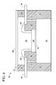
- FIG. 4 illustrates, in a simplified cross-sectional view, a subsequent stage of manufacture of packaged semiconductor device 100 , including encapsulated portions of the formed assembly ( FIG. 2 ) along with sintered die attach material 408 .
- FAM tool 302 is inserted into mold cavity 102 with the FAM tool surface contacting the film 304 causing a portion of the film to conform ( 402 ) to the FAM tool surface.
- a vacuum may be applied to enhance conforming the portion of the film to the FAM tool surface.
- regions of mold cavity 102 are partitioned by conformed film portion 402 contacting portions of the formed assembly at leads 106 and 108 and semiconductor die 202 .
- This allows for at least portions of the assembly to be encapsulated with a molding compound 404 .
- it is desired to prevent molding compound from completely covering the semiconductor die 202 , and thereby forming an air cavity above the semiconductor die 202 .
- the die attach material 204 is sintered concurrently with molten mold compound injected into cavity partitions formed by the FAM tool 302 and conformed film portion 402 .
- heat 406 may be applied to the FAM tool 302 sufficient to cause the die attach material 204 to sinter, while molten mold compound is injected into the desired regions of mold cavity 102 .
- heat 406 sufficient to sinter the die attach material 204 may be applied in any number of ways such as applying heat to the substrate 104 in addition to or instead of applying heat to FAM tool 302 .
- the elevated temperature of injected molten mold compound may assist sintering the die attach material 204 .
- forming the air cavity above the semiconductor die 202 and forming the sintered die attach material 408 are performed concurrently.
- the steps of forming the air cavity above the semiconductor die 202 and forming the sintered die attach material 408 are performed without retracting the FAM tool 302 . Because these steps are performed concurrently with the FAM tool 302 remaining inserted, manufacturing cycle times and costs are reduced.
- FIG. 5 illustrates, in a simplified cross-sectional view, a subsequent stage of manufacture of packaged semiconductor device 100 , including air cavity 502 above semiconductor die 202 .
- the FAM tool 302 is retracted from the mold cavity 102 and film 304 with conformed film portion 402 are removed, leaving air cavity 502 above semiconductor die 202 and portions of leads 106 and 108 exposed.
- FIG. 6 illustrates, in a simplified cross-sectional view, a subsequent stage of manufacture of packaged semiconductor device 100 , including wire bonds 602 and 604 , and attached lid 606 .
- Wire bonds are formed between locations on the semiconductor die 202 and leads 106 and 108 .
- the locations on the semiconductor die may include bond pads (not shown) and may be formed of any suitable metal such as aluminum, copper, silver, nickel, or the like for example.
- the leads 106 and 108 may be formed of any suitable electrically conductive material, such as aluminum, copper, nickel, or iron, or alloys including one or more of these materials, such as copper- 194 for example.
- Wire bond regions of leads 106 and 108 may be bare, or may be plated with any suitable metal such as Ag, Ni, NiPd, NiPdAu, for example.
- Bond wires electrically couple locations on the semiconductor die 202 to the leads 106 and 108 , forming wire bonds.
- the bond wires may be formed of a metal comprising aluminum, copper, silver, or gold.
- the bond wires may be attached to the locations on semiconductor die 202 and the leads 106 and 108 with either ball bonds or wedge bonds or a combination of ball bonds and wedge bonds.
- ball bonds may be used to attach a first end of bond wires to bond pads on the semiconductor die 202 and wedge bonds may be used to attach the opposite ends of bond wires to the leads 106 and 108 .
- the lid 606 is attached over the air cavity 502 .
- the lid 606 may serve to further protect the semiconductor die 202 .
- Lid 606 may be formed of any suitable material such as plastic, ceramic, glass, metal, and the like. Lid 606 may be attached with any suitable adhesive material at interfaces formed with mold compound 404 .
- lid 606 may be attached over the air cavity 502 using an epoxy material at interfaces with mold compound 404 .
- the lid 606 may also be ultrasonically joined with mold compound 404 , in a similar manner as multilayer liquid crystal polymer (LCP) materials are joined. In this embodiment, with lid 606 attached, a hermetic seal is formed over cavity 502 .
- LCP multilayer liquid crystal polymer
- the lid 606 may include one or more small openings or holes to allow air to pass through it which is especially useful for enclosing a pressure sensor, for example.
- lid 606 may be formed as a diaphragm to accommodate one or more sensors included on semiconductor die 202 .
- an efficient semiconductor device packaging process includes using a film-assisted molding technique to create an air cavity on top of a semiconductor die, and concurrently, providing heat and pressure for a sintering die attach process.
- the efficient semiconductor device packaging process enables a sintered die attach and air cavity formation in a single process step.
- a method of manufacturing a packaged semiconductor device including forming an assembly by placing a semiconductor die over a substrate with a die attach material between the semiconductor die and the substrate; contacting with a conformal structure at least a portion of a top surface of the semiconductor die, the conformal structure including a pressure transmissive material; applying a pressure to the conformal structure, the pressure transmitted to the top surface of the semiconductor die by the pressure transmissive material; while applying the pressure: encapsulating the assembly with a molding compound, wherein the at least a portion of the top surface of the semiconductor die contacted by the conformal structure is not encapsulated with molding compound; and exposing the assembly to a temperature that is sufficient to cause the die attach material to sinter.
- the assembly may further include a conductive lead, wherein contacting with a conformal structure further includes contacting a portion of the conductive lead, and wherein encapsulating the assembly with a molding compound further includes the portion of the conductive lead contacted by the conformal structure is not encapsulated with molding compound.
- the method may further include removing the conformal structure forming an air cavity above the semiconductor die.
- the method may further include after forming the air cavity above the semiconductor die, forming a wire bond between a location on the semiconductor die and the conductive lead.
- the method may further include attaching a lid over the air cavity formed above the semiconductor die. At least a portion of the bottom side of the substrate may be exposed after encapsulating the assembly.
- the substrate may include a metal material and wherein the substrate may be configured for dissipating heat.
- the die attach material may include a silver (Ag) material, and may be applied to the substrate in the form of a paste.
- the die attach material may include a silver (Ag) material, and may be applied in the form of a film or tape to a bottom surface of the semiconductor die.
- the method may further include supporting the conductive lead with a staking structure.
- the method may further include supporting the conductive lead with a retractable staking pin, the retractable staking pin retracted during encapsulating the assembly with a molding compound.
- a method of manufacturing a packaged semiconductor device including: forming an assembly including: a substrate having a top surface and a bottom surface, a semiconductor die over the substrate with a die attach material between the semiconductor die and the top surface of the substrate, and a conductive lead separate from the semiconductor die; contacting with a conformal film at least a portion of a top surface of the semiconductor die, the conformal film including a pressure transmissive material; applying a pressure to the conformal film, the pressure transmitted to the top surface of the semiconductor die by the pressure transmissive material; while applying the pressure: encapsulating the assembly with a molding compound, wherein the at least a portion of the top surface of the semiconductor die contacted by the conformal structure is not encapsulated with molding compound; and exposing the assembly to a temperature that is sufficient to cause the die attach material to sinter.
- the method may further include forming an air cavity above the semiconductor die, and after forming the air cavity forming a wire bond between a location on the semiconductor die and the conductive lead.
- the method may further include attaching a lid over the air cavity formed above the semiconductor die. At least a portion of the bottom side of the substrate may be exposed after encapsulating the assembly.
- the substrate may include a metal material and wherein the substrate may be configured for dissipating heat.
- the die attach material may include a silver (Ag) material.
- a packaged semiconductor device including: an assembly including: a substrate having a top surface and a bottom surface, a semiconductor die over the substrate with a sintered die attach material formed between the semiconductor die and the top surface of the substrate, and a conductive lead separate from the semiconductor die; an encapsulant encapsulating a portion of the assembly; a cavity formed in the encapsulant above at least a portion of the semiconductor die, the cavity formed concurrently with the sintered die attach material; and a lid attached over the cavity.
- the sintered die attach material may include a silver (Ag) material. At least a portion of the bottom surface of the substrate may be exposed after encapsulating the assembly.
- Coupled is not intended to be limited to a direct coupling or a mechanical coupling.
Abstract
Description
Claims (17)
Priority Applications (2)
| Application Number | Priority Date | Filing Date | Title |
|---|---|---|---|
| US15/079,276 US9799580B2 (en) | 2016-03-24 | 2016-03-24 | Semiconductor device package and methods of manufacture thereof |
| US15/710,098 US10825747B2 (en) | 2016-03-24 | 2017-09-20 | Semiconductor device package and methods of manufacture thereof |
Applications Claiming Priority (1)
| Application Number | Priority Date | Filing Date | Title |
|---|---|---|---|
| US15/079,276 US9799580B2 (en) | 2016-03-24 | 2016-03-24 | Semiconductor device package and methods of manufacture thereof |
Related Child Applications (1)
| Application Number | Title | Priority Date | Filing Date |
|---|---|---|---|
| US15/710,098 Division US10825747B2 (en) | 2016-03-24 | 2017-09-20 | Semiconductor device package and methods of manufacture thereof |
Publications (2)
| Publication Number | Publication Date |
|---|---|
| US20170278763A1 US20170278763A1 (en) | 2017-09-28 |
| US9799580B2 true US9799580B2 (en) | 2017-10-24 |
Family
ID=59898523
Family Applications (2)
| Application Number | Title | Priority Date | Filing Date |
|---|---|---|---|
| US15/079,276 Active US9799580B2 (en) | 2016-03-24 | 2016-03-24 | Semiconductor device package and methods of manufacture thereof |
| US15/710,098 Active 2036-06-29 US10825747B2 (en) | 2016-03-24 | 2017-09-20 | Semiconductor device package and methods of manufacture thereof |
Family Applications After (1)
| Application Number | Title | Priority Date | Filing Date |
|---|---|---|---|
| US15/710,098 Active 2036-06-29 US10825747B2 (en) | 2016-03-24 | 2017-09-20 | Semiconductor device package and methods of manufacture thereof |
Country Status (1)
| Country | Link |
|---|---|
| US (2) | US9799580B2 (en) |
Cited By (2)
| Publication number | Priority date | Publication date | Assignee | Title |
|---|---|---|---|---|
| US10910326B2 (en) * | 2016-11-17 | 2021-02-02 | Mitsubishi Electric Corporation | Semiconductor package |
| US11128268B1 (en) | 2020-05-28 | 2021-09-21 | Nxp Usa, Inc. | Power amplifier packages containing peripherally-encapsulated dies and methods for the fabrication thereof |
Families Citing this family (9)
| Publication number | Priority date | Publication date | Assignee | Title |
|---|---|---|---|---|
| US11024595B2 (en) * | 2017-06-16 | 2021-06-01 | Micron Technology, Inc. | Thermocompression bond tips and related apparatus and methods |
| US10431526B2 (en) * | 2017-10-09 | 2019-10-01 | Cree, Inc. | Rivetless lead fastening for a semiconductor package |
| DE102018100946A1 (en) * | 2018-01-17 | 2019-07-18 | Osram Opto Semiconductors Gmbh | COMPONENT AND METHOD FOR PRODUCING A COMPONENT |
| US11393778B2 (en) * | 2018-12-05 | 2022-07-19 | Mitsubishi Electric Corporation | Semiconductor device and antenna device |
| MY196394A (en) * | 2019-01-04 | 2023-03-28 | Carsem M Sdn Bhd | Molded Integrated Circuit Packages |
| TWI741483B (en) * | 2019-05-28 | 2021-10-01 | 大陸商武漢杰開科技有限公司 | Multi-device packaging structure and manufacturing method thereof |
| US20210013375A1 (en) * | 2019-07-11 | 2021-01-14 | Advanced Semiconductor Engineering, Inc. | Semiconductor device package and method of manufacturing the same |
| US11387373B2 (en) * | 2019-07-29 | 2022-07-12 | Nxp Usa, Inc. | Low drain-source on resistance semiconductor component and method of fabrication |
| US11410964B2 (en) * | 2019-11-22 | 2022-08-09 | Micron Technology, Inc. | Contaminant control in thermocompression bonding of semiconductors and associated systems and methods |
Citations (11)
| Publication number | Priority date | Publication date | Assignee | Title |
|---|---|---|---|---|
| US4888307A (en) * | 1986-08-27 | 1989-12-19 | Sgs Microelettronica S.P.A. | Method for manufacturing plastic encapsulated semiconductor devices |
| US6420779B1 (en) | 1999-09-14 | 2002-07-16 | St Assembly Test Services Ltd. | Leadframe based chip scale package and method of producing the same |
| US6921971B2 (en) * | 2003-01-15 | 2005-07-26 | Kyocera Corporation | Heat releasing member, package for accommodating semiconductor element and semiconductor device |
| US7435619B2 (en) | 2006-02-14 | 2008-10-14 | Stats Chippac Ltd. | Method of fabricating a 3-D package stacking system |
| US7445967B2 (en) | 2006-01-20 | 2008-11-04 | Freescale Semiconductor, Inc. | Method of packaging a semiconductor die and package thereof |
| US7901971B2 (en) * | 2008-08-11 | 2011-03-08 | Sensirion Ag | Method for manufacturing a sensor device with a stress relief layer |
| US20130221511A1 (en) * | 2012-02-23 | 2013-08-29 | Leo M. Higgins, III | Method for forming die assembly with heat spreader |
| US20140070397A1 (en) * | 2012-09-13 | 2014-03-13 | Lakshminarayan Viswanathan | High power semiconductor package subsystems |
| US8835299B2 (en) | 2012-08-29 | 2014-09-16 | Infineon Technologies Ag | Pre-sintered semiconductor die structure |
| US9099567B2 (en) | 2013-11-25 | 2015-08-04 | Freescale Semiconductor, Inc. | Packaged semiconductor devices and methods of their fabrication |
| US20160172559A1 (en) * | 2013-07-04 | 2016-06-16 | Osram Opto Semiconductors Gmbh | Method for Producing an Optoelectronic Device |
Family Cites Families (7)
| Publication number | Priority date | Publication date | Assignee | Title |
|---|---|---|---|---|
| JPH02306639A (en) * | 1989-05-22 | 1990-12-20 | Toshiba Corp | Resin encapsulating method for semiconductor device |
| US5455386A (en) * | 1994-01-14 | 1995-10-03 | Olin Corporation | Chamfered electronic package component |
| KR970005706B1 (en) * | 1994-01-24 | 1997-04-19 | 금성일렉트론 주식회사 | Ccd and the manufacturing method |
| US6453749B1 (en) * | 1999-10-28 | 2002-09-24 | Motorola, Inc. | Physical sensor component |
| JP3733114B2 (en) * | 2000-07-25 | 2006-01-11 | 株式会社メヂアナ電子 | Plastic package base and air cavity package |
| US8069549B2 (en) * | 2007-03-22 | 2011-12-06 | Seiko Epson Corporation | Method for sealing a quartz crystal device |
| EP3056467B1 (en) * | 2013-02-20 | 2017-05-24 | Harman Becker Automotive Systems GmbH | Circuit board comprising spatial light modulator |
-
2016
- 2016-03-24 US US15/079,276 patent/US9799580B2/en active Active
-
2017
- 2017-09-20 US US15/710,098 patent/US10825747B2/en active Active
Patent Citations (11)
| Publication number | Priority date | Publication date | Assignee | Title |
|---|---|---|---|---|
| US4888307A (en) * | 1986-08-27 | 1989-12-19 | Sgs Microelettronica S.P.A. | Method for manufacturing plastic encapsulated semiconductor devices |
| US6420779B1 (en) | 1999-09-14 | 2002-07-16 | St Assembly Test Services Ltd. | Leadframe based chip scale package and method of producing the same |
| US6921971B2 (en) * | 2003-01-15 | 2005-07-26 | Kyocera Corporation | Heat releasing member, package for accommodating semiconductor element and semiconductor device |
| US7445967B2 (en) | 2006-01-20 | 2008-11-04 | Freescale Semiconductor, Inc. | Method of packaging a semiconductor die and package thereof |
| US7435619B2 (en) | 2006-02-14 | 2008-10-14 | Stats Chippac Ltd. | Method of fabricating a 3-D package stacking system |
| US7901971B2 (en) * | 2008-08-11 | 2011-03-08 | Sensirion Ag | Method for manufacturing a sensor device with a stress relief layer |
| US20130221511A1 (en) * | 2012-02-23 | 2013-08-29 | Leo M. Higgins, III | Method for forming die assembly with heat spreader |
| US8835299B2 (en) | 2012-08-29 | 2014-09-16 | Infineon Technologies Ag | Pre-sintered semiconductor die structure |
| US20140070397A1 (en) * | 2012-09-13 | 2014-03-13 | Lakshminarayan Viswanathan | High power semiconductor package subsystems |
| US20160172559A1 (en) * | 2013-07-04 | 2016-06-16 | Osram Opto Semiconductors Gmbh | Method for Producing an Optoelectronic Device |
| US9099567B2 (en) | 2013-11-25 | 2015-08-04 | Freescale Semiconductor, Inc. | Packaged semiconductor devices and methods of their fabrication |
Non-Patent Citations (5)
| Title |
|---|
| "Advanced Molding and Sintering Systems"; Boschman Technologies, www.boschman.nl, 2016. |
| "Heraeus-Besi-Industrial Sintering Process-Brochure (2013)"; www.heraeus-electronics.com, 2016. |
| Gobl, C., "Low Temperature Sinter Technology Die Attachment for Power Electronics Applications"; CIPS 2010, Mar. 16-18, 2010, Nuremberg/Germany. |
| Li, J., "Bonding Strength of multiple SiC die attachment prepared by sintering of Ag nan particles"; Journal of Material Processing Technology, 215 (2015) 299-308. |
| Siow, K., "Are Sintered Silver Joints Ready for Use as Interconnect Material in Microelectronic Packaging?"; Journal of Electronic Materials, vol. 43, No. 4, 2014. |
Cited By (2)
| Publication number | Priority date | Publication date | Assignee | Title |
|---|---|---|---|---|
| US10910326B2 (en) * | 2016-11-17 | 2021-02-02 | Mitsubishi Electric Corporation | Semiconductor package |
| US11128268B1 (en) | 2020-05-28 | 2021-09-21 | Nxp Usa, Inc. | Power amplifier packages containing peripherally-encapsulated dies and methods for the fabrication thereof |
Also Published As
| Publication number | Publication date |
|---|---|
| US20180012815A1 (en) | 2018-01-11 |
| US10825747B2 (en) | 2020-11-03 |
| US20170278763A1 (en) | 2017-09-28 |
Similar Documents
| Publication | Publication Date | Title |
|---|---|---|
| US10825747B2 (en) | Semiconductor device package and methods of manufacture thereof | |
| US9425161B2 (en) | Semiconductor device with mechanical lock features between a semiconductor die and a substrate | |
| US10211177B2 (en) | High power semiconductor package subsystems | |
| US8836101B2 (en) | Multi-chip semiconductor packages and assembly thereof | |
| US9263375B2 (en) | System, method and apparatus for leadless surface mounted semiconductor package | |
| US8735223B2 (en) | Semiconductor devices and methods of assembling same | |
| US8049313B2 (en) | Heat spreader for semiconductor package | |
| US9837327B2 (en) | Methods for forming semiconductor device packages | |
| JPH08255860A (en) | Lead frame, and method for forming lead frame | |
| US20080020517A1 (en) | Multi Lead Frame Power Package | |
| US9887149B2 (en) | Cavity package with die attach pad | |
| US20220189856A1 (en) | Die attachment for semiconductor device packaging and method therefor | |
| US7075174B2 (en) | Semiconductor packaging techniques for use with non-ceramic packages | |
| US9691637B2 (en) | Method for packaging an integrated circuit device with stress buffer | |
| US9601400B2 (en) | Glass/ceramic replacement of epoxy for high temperature hermetically sealed non-axial electronic packages | |
| US9230874B1 (en) | Integrated circuit package with a heat conductor | |
| JPH0338057A (en) | Flagless lead frame, and package using it, and manufacture | |
| US20240105579A1 (en) | Extendable inner lead for leaded package | |
| CN113097076A (en) | QFN frame structure, QFN packaging structure and manufacturing method | |
| JPH03265161A (en) | Resin-sealed semiconductor device | |
| TW432646B (en) | Manufacturing method for semiconductor chip packaging structure with no outer leads | |
| US20150206769A1 (en) | Lead frame based semiconductor device with power bars | |
| JP2007142226A (en) | Semiconductor device and method of manufacturing same, and method of manufacturing lead frame used therefor | |
| JP2000349223A (en) | Semiconductor device with lead frame where bonding and heat dissipation are balanced with each other | |
| KR20040048451A (en) | method for fabricating semiconductor package |
Legal Events
| Date | Code | Title | Description |
|---|---|---|---|
| AS | Assignment |
Owner name: FREESCALE SEMICONDUCTOR, INC., TEXAS Free format text: ASSIGNMENT OF ASSIGNORS INTEREST;ASSIGNORS:LI, LI;MOLLA, JAYNAL A.;VISWANATHAN, LAKSHMINARAYAN;REEL/FRAME:038102/0849 Effective date: 20160322 |
|
| AS | Assignment |
Owner name: MORGAN STANLEY SENIOR FUNDING, INC., MARYLAND Free format text: SUPPLEMENT TO THE SECURITY AGREEMENT;ASSIGNOR:FREESCALE SEMICONDUCTOR, INC.;REEL/FRAME:039138/0001 Effective date: 20160525 |
|
| AS | Assignment |
Owner name: NXP USA, INC., TEXAS Free format text: CHANGE OF NAME;ASSIGNOR:FREESCALE SEMICONDUCTOR INC.;REEL/FRAME:040626/0683 Effective date: 20161107 |
|
| AS | Assignment |
Owner name: NXP USA, INC., TEXAS Free format text: CORRECTIVE ASSIGNMENT TO CORRECT THE NATURE OF CONVEYANCE PREVIOUSLY RECORDED AT REEL: 040626 FRAME: 0683. ASSIGNOR(S) HEREBY CONFIRMS THE MERGER AND CHANGE OF NAME EFFECTIVE NOVEMBER 7, 2016;ASSIGNORS:NXP SEMICONDUCTORS USA, INC. (MERGED INTO);FREESCALE SEMICONDUCTOR, INC. (UNDER);SIGNING DATES FROM 20161104 TO 20161107;REEL/FRAME:041414/0883 |
|
| STCF | Information on status: patent grant |
Free format text: PATENTED CASE |
|
| AS | Assignment |
Owner name: NXP B.V., NETHERLANDS Free format text: RELEASE BY SECURED PARTY;ASSIGNOR:MORGAN STANLEY SENIOR FUNDING, INC.;REEL/FRAME:050744/0097 Effective date: 20190903 |
|
| MAFP | Maintenance fee payment |
Free format text: PAYMENT OF MAINTENANCE FEE, 4TH YEAR, LARGE ENTITY (ORIGINAL EVENT CODE: M1551); ENTITY STATUS OF PATENT OWNER: LARGE ENTITY Year of fee payment: 4 |