US9768091B2 - Method of forming an electronic package and structure - Google Patents
Method of forming an electronic package and structure Download PDFInfo
- Publication number
- US9768091B2 US9768091B2 US13/408,058 US201213408058A US9768091B2 US 9768091 B2 US9768091 B2 US 9768091B2 US 201213408058 A US201213408058 A US 201213408058A US 9768091 B2 US9768091 B2 US 9768091B2
- Authority
- US
- United States
- Prior art keywords
- pads
- electronic device
- adjacent inner
- pair
- inner rows
- Prior art date
- Legal status (The legal status is an assumption and is not a legal conclusion. Google has not performed a legal analysis and makes no representation as to the accuracy of the status listed.)
- Active, expires
Links
Images


Classifications
-
- H—ELECTRICITY
- H01—ELECTRIC ELEMENTS
- H01L—SEMICONDUCTOR DEVICES NOT COVERED BY CLASS H10
- H01L23/00—Details of semiconductor or other solid state devices
- H01L23/28—Encapsulations, e.g. encapsulating layers, coatings, e.g. for protection
- H01L23/31—Encapsulations, e.g. encapsulating layers, coatings, e.g. for protection characterised by the arrangement or shape
- H01L23/3107—Encapsulations, e.g. encapsulating layers, coatings, e.g. for protection characterised by the arrangement or shape the device being completely enclosed
-
- H—ELECTRICITY
- H01—ELECTRIC ELEMENTS
- H01L—SEMICONDUCTOR DEVICES NOT COVERED BY CLASS H10
- H01L21/00—Processes or apparatus adapted for the manufacture or treatment of semiconductor or solid state devices or of parts thereof
- H01L21/02—Manufacture or treatment of semiconductor devices or of parts thereof
- H01L21/04—Manufacture or treatment of semiconductor devices or of parts thereof the devices having at least one potential-jump barrier or surface barrier, e.g. PN junction, depletion layer or carrier concentration layer
- H01L21/48—Manufacture or treatment of parts, e.g. containers, prior to assembly of the devices, using processes not provided for in a single one of the subgroups H01L21/06 - H01L21/326
- H01L21/4814—Conductive parts
- H01L21/4821—Flat leads, e.g. lead frames with or without insulating supports
-
- H—ELECTRICITY
- H01—ELECTRIC ELEMENTS
- H01L—SEMICONDUCTOR DEVICES NOT COVERED BY CLASS H10
- H01L23/00—Details of semiconductor or other solid state devices
- H01L23/48—Arrangements for conducting electric current to or from the solid state body in operation, e.g. leads, terminal arrangements ; Selection of materials therefor
- H01L23/488—Arrangements for conducting electric current to or from the solid state body in operation, e.g. leads, terminal arrangements ; Selection of materials therefor consisting of soldered or bonded constructions
- H01L23/495—Lead-frames or other flat leads
- H01L23/49503—Lead-frames or other flat leads characterised by the die pad
- H01L23/4951—Chip-on-leads or leads-on-chip techniques, i.e. inner lead fingers being used as die pad
-
- H—ELECTRICITY
- H01—ELECTRIC ELEMENTS
- H01L—SEMICONDUCTOR DEVICES NOT COVERED BY CLASS H10
- H01L23/00—Details of semiconductor or other solid state devices
- H01L23/48—Arrangements for conducting electric current to or from the solid state body in operation, e.g. leads, terminal arrangements ; Selection of materials therefor
- H01L23/488—Arrangements for conducting electric current to or from the solid state body in operation, e.g. leads, terminal arrangements ; Selection of materials therefor consisting of soldered or bonded constructions
- H01L23/495—Lead-frames or other flat leads
- H01L23/49541—Geometry of the lead-frame
- H01L23/49548—Cross section geometry
-
- H—ELECTRICITY
- H01—ELECTRIC ELEMENTS
- H01L—SEMICONDUCTOR DEVICES NOT COVERED BY CLASS H10
- H01L24/00—Arrangements for connecting or disconnecting semiconductor or solid-state bodies; Methods or apparatus related thereto
- H01L24/93—Batch processes
- H01L24/95—Batch processes at chip-level, i.e. with connecting carried out on a plurality of singulated devices, i.e. on diced chips
- H01L24/97—Batch processes at chip-level, i.e. with connecting carried out on a plurality of singulated devices, i.e. on diced chips the devices being connected to a common substrate, e.g. interposer, said common substrate being separable into individual assemblies after connecting
-
- H—ELECTRICITY
- H01—ELECTRIC ELEMENTS
- H01L—SEMICONDUCTOR DEVICES NOT COVERED BY CLASS H10
- H01L2224/00—Indexing scheme for arrangements for connecting or disconnecting semiconductor or solid-state bodies and methods related thereto as covered by H01L24/00
- H01L2224/01—Means for bonding being attached to, or being formed on, the surface to be connected, e.g. chip-to-package, die-attach, "first-level" interconnects; Manufacturing methods related thereto
- H01L2224/26—Layer connectors, e.g. plate connectors, solder or adhesive layers; Manufacturing methods related thereto
- H01L2224/31—Structure, shape, material or disposition of the layer connectors after the connecting process
- H01L2224/32—Structure, shape, material or disposition of the layer connectors after the connecting process of an individual layer connector
- H01L2224/321—Disposition
- H01L2224/32151—Disposition the layer connector connecting between a semiconductor or solid-state body and an item not being a semiconductor or solid-state body, e.g. chip-to-substrate, chip-to-passive
- H01L2224/32221—Disposition the layer connector connecting between a semiconductor or solid-state body and an item not being a semiconductor or solid-state body, e.g. chip-to-substrate, chip-to-passive the body and the item being stacked
- H01L2224/32245—Disposition the layer connector connecting between a semiconductor or solid-state body and an item not being a semiconductor or solid-state body, e.g. chip-to-substrate, chip-to-passive the body and the item being stacked the item being metallic
-
- H—ELECTRICITY
- H01—ELECTRIC ELEMENTS
- H01L—SEMICONDUCTOR DEVICES NOT COVERED BY CLASS H10
- H01L2224/00—Indexing scheme for arrangements for connecting or disconnecting semiconductor or solid-state bodies and methods related thereto as covered by H01L24/00
- H01L2224/01—Means for bonding being attached to, or being formed on, the surface to be connected, e.g. chip-to-package, die-attach, "first-level" interconnects; Manufacturing methods related thereto
- H01L2224/42—Wire connectors; Manufacturing methods related thereto
- H01L2224/47—Structure, shape, material or disposition of the wire connectors after the connecting process
- H01L2224/48—Structure, shape, material or disposition of the wire connectors after the connecting process of an individual wire connector
- H01L2224/481—Disposition
- H01L2224/48151—Connecting between a semiconductor or solid-state body and an item not being a semiconductor or solid-state body, e.g. chip-to-substrate, chip-to-passive
- H01L2224/48221—Connecting between a semiconductor or solid-state body and an item not being a semiconductor or solid-state body, e.g. chip-to-substrate, chip-to-passive the body and the item being stacked
- H01L2224/48245—Connecting between a semiconductor or solid-state body and an item not being a semiconductor or solid-state body, e.g. chip-to-substrate, chip-to-passive the body and the item being stacked the item being metallic
- H01L2224/48247—Connecting between a semiconductor or solid-state body and an item not being a semiconductor or solid-state body, e.g. chip-to-substrate, chip-to-passive the body and the item being stacked the item being metallic connecting the wire to a bond pad of the item
-
- H—ELECTRICITY
- H01—ELECTRIC ELEMENTS
- H01L—SEMICONDUCTOR DEVICES NOT COVERED BY CLASS H10
- H01L2224/00—Indexing scheme for arrangements for connecting or disconnecting semiconductor or solid-state bodies and methods related thereto as covered by H01L24/00
- H01L2224/73—Means for bonding being of different types provided for in two or more of groups H01L2224/10, H01L2224/18, H01L2224/26, H01L2224/34, H01L2224/42, H01L2224/50, H01L2224/63, H01L2224/71
- H01L2224/732—Location after the connecting process
- H01L2224/73251—Location after the connecting process on different surfaces
- H01L2224/73265—Layer and wire connectors
-
- H—ELECTRICITY
- H01—ELECTRIC ELEMENTS
- H01L—SEMICONDUCTOR DEVICES NOT COVERED BY CLASS H10
- H01L2224/00—Indexing scheme for arrangements for connecting or disconnecting semiconductor or solid-state bodies and methods related thereto as covered by H01L24/00
- H01L2224/80—Methods for connecting semiconductor or other solid state bodies using means for bonding being attached to, or being formed on, the surface to be connected
- H01L2224/83—Methods for connecting semiconductor or other solid state bodies using means for bonding being attached to, or being formed on, the surface to be connected using a layer connector
-
- H—ELECTRICITY
- H01—ELECTRIC ELEMENTS
- H01L—SEMICONDUCTOR DEVICES NOT COVERED BY CLASS H10
- H01L2224/00—Indexing scheme for arrangements for connecting or disconnecting semiconductor or solid-state bodies and methods related thereto as covered by H01L24/00
- H01L2224/80—Methods for connecting semiconductor or other solid state bodies using means for bonding being attached to, or being formed on, the surface to be connected
- H01L2224/85—Methods for connecting semiconductor or other solid state bodies using means for bonding being attached to, or being formed on, the surface to be connected using a wire connector
-
- H—ELECTRICITY
- H01—ELECTRIC ELEMENTS
- H01L—SEMICONDUCTOR DEVICES NOT COVERED BY CLASS H10
- H01L2224/00—Indexing scheme for arrangements for connecting or disconnecting semiconductor or solid-state bodies and methods related thereto as covered by H01L24/00
- H01L2224/93—Batch processes
- H01L2224/95—Batch processes at chip-level, i.e. with connecting carried out on a plurality of singulated devices, i.e. on diced chips
- H01L2224/97—Batch processes at chip-level, i.e. with connecting carried out on a plurality of singulated devices, i.e. on diced chips the devices being connected to a common substrate, e.g. interposer, said common substrate being separable into individual assemblies after connecting
-
- H—ELECTRICITY
- H01—ELECTRIC ELEMENTS
- H01L—SEMICONDUCTOR DEVICES NOT COVERED BY CLASS H10
- H01L24/00—Arrangements for connecting or disconnecting semiconductor or solid-state bodies; Methods or apparatus related thereto
- H01L24/73—Means for bonding being of different types provided for in two or more of groups H01L24/10, H01L24/18, H01L24/26, H01L24/34, H01L24/42, H01L24/50, H01L24/63, H01L24/71
-
- H—ELECTRICITY
- H01—ELECTRIC ELEMENTS
- H01L—SEMICONDUCTOR DEVICES NOT COVERED BY CLASS H10
- H01L2924/00—Indexing scheme for arrangements or methods for connecting or disconnecting semiconductor or solid-state bodies as covered by H01L24/00
-
- H—ELECTRICITY
- H01—ELECTRIC ELEMENTS
- H01L—SEMICONDUCTOR DEVICES NOT COVERED BY CLASS H10
- H01L2924/00—Indexing scheme for arrangements or methods for connecting or disconnecting semiconductor or solid-state bodies as covered by H01L24/00
- H01L2924/0001—Technical content checked by a classifier
- H01L2924/00012—Relevant to the scope of the group, the symbol of which is combined with the symbol of this group
-
- H—ELECTRICITY
- H01—ELECTRIC ELEMENTS
- H01L—SEMICONDUCTOR DEVICES NOT COVERED BY CLASS H10
- H01L2924/00—Indexing scheme for arrangements or methods for connecting or disconnecting semiconductor or solid-state bodies as covered by H01L24/00
- H01L2924/06—Polymers
- H01L2924/078—Adhesive characteristics other than chemical
- H01L2924/07802—Adhesive characteristics other than chemical not being an ohmic electrical conductor
-
- H—ELECTRICITY
- H01—ELECTRIC ELEMENTS
- H01L—SEMICONDUCTOR DEVICES NOT COVERED BY CLASS H10
- H01L2924/00—Indexing scheme for arrangements or methods for connecting or disconnecting semiconductor or solid-state bodies as covered by H01L24/00
- H01L2924/15—Details of package parts other than the semiconductor or other solid state devices to be connected
- H01L2924/151—Die mounting substrate
- H01L2924/1515—Shape
- H01L2924/15151—Shape the die mounting substrate comprising an aperture, e.g. for underfilling, outgassing, window type wire connections
-
- H—ELECTRICITY
- H01—ELECTRIC ELEMENTS
- H01L—SEMICONDUCTOR DEVICES NOT COVERED BY CLASS H10
- H01L2924/00—Indexing scheme for arrangements or methods for connecting or disconnecting semiconductor or solid-state bodies as covered by H01L24/00
- H01L2924/15—Details of package parts other than the semiconductor or other solid state devices to be connected
- H01L2924/181—Encapsulation
-
- Y—GENERAL TAGGING OF NEW TECHNOLOGICAL DEVELOPMENTS; GENERAL TAGGING OF CROSS-SECTIONAL TECHNOLOGIES SPANNING OVER SEVERAL SECTIONS OF THE IPC; TECHNICAL SUBJECTS COVERED BY FORMER USPC CROSS-REFERENCE ART COLLECTIONS [XRACs] AND DIGESTS
- Y10—TECHNICAL SUBJECTS COVERED BY FORMER USPC
- Y10T—TECHNICAL SUBJECTS COVERED BY FORMER US CLASSIFICATION
- Y10T29/00—Metal working
- Y10T29/49—Method of mechanical manufacture
- Y10T29/49002—Electrical device making
- Y10T29/49117—Conductor or circuit manufacturing
Definitions
- This document relates generally to electronic devices, and more specifically to methods of forming packaged electronics devices and structures.
- I/O input/output
- the I/O pads were placed in a single row configuration around the flag portion, or they were placed in a multi-row configuration around the flag portion. The multi-row I/O configurations were desired to support higher pin-count devices.
- One previous QFN package with a multi-row I/O configuration used staggered or alternating I/O pads that were held together in a leadframe with tie bars until final assembly when the I/O pads were all separated into individual pads.
- the outer rows of I/O pads were held together using a tie bar, and the inner row of I/O pads was tied to the flag until final assembly when the I/O pads and the flag were all separated into individual and isolated structures.
- the assembled package consisted of a separate and distinct flag portion that held the semiconductor chip, a separate and distinct inner row of I/O pads, and a separate and distinct outer row of I/O pads.
- FIG. 1 illustrates a partially transparent perspective view of an electronic structure in accordance with a first embodiment of the present invention
- FIG. 2 illustrates a perspective view of the electronic structure in accordance with the first embodiment
- FIG. 3 illustrates a perspective view of a lead frame structure in accordance with an embodiment of the present invention
- FIG. 4 illustrates a perspective view of the lead frame structure of FIG. 3 after further processing
- FIGS. 5-9 illustrate cross-sectional views of an electronic package structure in accordance with the present invention at various stages of fabrication.
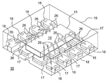
- FIG. 1 shows a perspective view of a packaged electronic device or structure 10 shown in a QFN-type configuration in accordance with a first embodiment.
- encapsulating layer 19 (described further in conjunction with FIG. 2 ) is shown as transparent to illustrate the inside structure of device 10 .
- device 10 may include an electronic chip or component 11 , which may be a physical component configured to affect the flow of electrons or their associated fields in a desired manner.
- chip 11 may comprise a semiconductor device, such as a discrete device, an integrated circuit device, an optoelectronic device, an electromechanical sensor device, combinations thereof, or the like.
- chip 11 may comprise, or may further comprise, a passive device or the like.
- chip 11 includes two opposing major surfaces 14 and 16 .
- Device 10 further includes conductive I/O pads or structures 17 and 18 formed in a multi-row or multiple row configuration as shown, for example, in FIG. 1 .
- I/O pads 17 and 18 may comprise, for example, metal materials, plated materials, and/or combinations thereof.
- I/O pads 17 and 18 may comprise a copper alloy.
- I/O pads 17 may form adjacent inner rows of I/O pads for device 10
- I/O pads 18 may form outer rows of I/O pads for device 10 .
- major surface 16 of chip 11 may be attached to portions of I/O pads 17 so that chip 11 partially overlaps adjacent rows of I/O pads 17 .
- the size of chip 11 may be selected so that the partial overlap configuration leaves portions of I/O pads 17 exposed to accommodate interconnect structures.
- I/O pads 17 are configured to both to provide physical support chip 11 and to function as I/O pads.
- device 10 is formed without or absent a flag portion as used in prior structures. In accordance with the present embodiment, this configuration provides a smaller size for device because, among other things, the separate flag portion used in prior structures is absent while still providing the benefit of multi-row I/O configuration. In prior structures the flag portion provided physical support for the chip, but was not used for wire bond connections. In another embodiment, only some of I/O pads 17 may support chip 11 .
- major surface 14 of chip 11 is connected to I/O pads 17 and 18 using connective structures 26 , which may comprise for example, wire bonds, ribbon bonds, clips, combinations thereof, or the like. Although not shown, major surface 14 may further include conductive bond pads for connecting connective structures 26 to the various components that may be integrated within chip 11 .
- FIG. 2 is a perspective view of device 10 including encapsulating layer 19 shown as non-transparent.
- encapsulating layer 19 may comprise a molded layer, which may enclose and protect portions of chip 11 , connective structures 26 , and I/O pads 17 and 18 .
- molded layer 19 may comprise a plastic material that may include resin, filler, pigments, reinforcements, plasticizers, and other materials.
- device 10 may include a gap, slot, or channel 35 in encapsulating layer 19 between adjacent I/O pads 17 , which may be formed as part of the assembly process as will be explained in more detail in conjunction with FIGS. 5-9 .
- FIG. 3 is a perspective view of a leadframe 30 in accordance with one embodiment. It is understood that leadframe 30 may be a portion of a larger structure having multiple leadframes 30 .
- leadframe 30 may include multiple rows of I/O pads 17 and 18 , with I/O pads 17 forming portions of inner rows, and I/O pads 18 forming outer rows in this embodiment. I/O pads 18 may be attached to tie bars 31 (only one is shown for ease of understanding), which are subsequently removed as will be described further in conjunction with FIGS. 5-9 .
- tie bars 31 only one is shown for ease of understanding
- lower portions of inner rows of I/O pads 17 are held together using a connective portion 32 , which may be further configured to leave a gap 33 between upper portions of adjacent rows of I/O pads 17 .
- connective portion 32 may be formed as a half-etched section of leadframe 30 between adjacent rows of inner I/O pads 17 .
- connective portion 32 is half-etched in a downward direction with respect to major surfaces 170 (for example, the surface where chip 11 will be attached) of I/O pads 17 .
- connective portion 32 is configured to hold I/O pads 17 together during the assembly process, and further configured for subsequent removal to isolate I/O pads 17 from each other in the final packaged device.
- I/O pads 171 and 172 are an example of a pair of opposing I/O pads in adjacent inner rows of I/O pads 17 .
- FIG. 4 shows the leadframe structure of FIG. 3 after additional processing.
- chip 11 may be placed onto major surfaces 170 of inner and adjacent rows of I/O pads 17 and overlying gap 33 and spaced apart from connective portion 32 .
- chip 11 may include a conductive layer 46 formed on major surface 16 , and conductive layer 46 may comprise, for example, a continuous or unpatterned metal layer or layers, such a titanium-nickel-silver, chromium-nickel-gold, or the like.
- chip 11 may be attached to I/O pads 17 using a non-conductive layer or material.
- chip 11 may be attached to I/O pads 17 using a non-conductive adhesive material, such as a non-conductive epoxy adhesive.
- the adhesive material may comprise a non-conductive material that includes one or more epoxide groups (for example, a resin material or a thermoset polymer) or the like.
- the adhesive material may comprise an AblestickTM brand of non-conductive adhesives, which are available from Henkel of Dusseldorf, Germany.
- chip 11 is attached to I/O pads using other intervening or intermediate bonding materials applied either to chip 11 or I/O pads 17 , which may be configured to insulate chip 11 from I/O pads 17 .
- Connective structures 26 may then be used to interconnect chip 11 to I/O pads 17 and 18 as shown in FIG. 3 , where wire bonds are shown as an example.
- one or more of I/O pads 17 may be connected or attached to major surface 16 with a conductive layer or material to provide a means for providing an electrical bias to major surface 16 of chip 11 , and other of I/O pads 17 may be connected or attached to major surface 16 with a non-conductive layer or material.
- a conductive adhesive such as a conductive epoxy adhesive, may be used for the conductive layer.
- a connective structure 126 may not connected to I/O pad 175 .
- FIG. 5 shows a partial cross-sectional view of a conductive leadframe 50 , which may comprises a conductive material, such as copper, a copper alloy, a plated structure, or the like.
- leadframe 50 includes multiple rows of I/O pads 117 and 118 .
- I/O pads 117 may be configured as adjacent inner rows of I/O pads for the electronic devices to be assembled, and I/O pads 118 may be configured as outer rows of I/O pads.
- adjacent rows of inner I/O pads 117 are spaced apart a connective portion 132 .
- connective portions 132 may be formed as half-etched portions, which may be etched downward with respect to major surfaces 1170 of I/O pads 117 . This configuration forms a gap 133 between adjacent I/O pads 117 .
- I/O pads 118 may be held together with tie bars 131 .
- tie bars 131 may be formed as half-etched portions, which may be etched upward with respect to major surfaces 1180 of I/O pads 118 .
- connective portions 132 and tie bars 131 may be formed by half-etching leadframe 50 from opposite major surfaces.
- connective portions 132 and tie bars 131 may be formed using other techniques such as stamping, milling, combinations thereof, or the like.
- FIG. 6 shows a partial cross-sectional view of leadframe 50 after additional processing.
- Chips 11 having optional conductive layers 46 overlying major surfaces 16 may be attached to major surfaces 1170 of inner I/O pads 117 using an optional bonding layer 47 .
- bonding layer 47 may comprise a non-conductive adhesive material, such as a non-conductive epoxy adhesive.
- one or more of I/O pads 117 may be attached to major surface 16 using a conductive layer, such as a conductive adhesive.
- chips 11 overlie gaps 133 , and partially overlap portions of major surfaces 1170 of adjacent inner I/O pads 117 .
- chips 11 overlie connective portions 132 without making physical contact to connective portions 132 because of gaps 133 .
- connective structures 126 which in this embodiment may comprise wire bonds, clips, ribbon bonds, combinations thereof, or the like.
- connective structures 126 may electrically connect bonding pads (not shown) on major surface 14 of chips 11 to I/O pads 117 and 118 .
- FIG. 7 shows a partial cross-sectional view of leadframe 50 after encapsulating layer 119 has been formed to cover portions of the structure while leaving major surfaces 1171 of I/O pads 117 and 1180 of I/O pads 118 exposed for connection to next levels of assembly, such as printed circuit boards.
- encapsulating layer 119 may comprise an over-molded layer.
- encapsulating layer 119 may comprise a cavity-molded layer.
- molded layer 119 may comprise a plastic material that may include resin, filler, pigments, reinforcements, plasticizers, and other materials.
- encapsulating layer 119 may fill gaps 133 during the molding process, which covers and protects exposed portions of major surfaces 16 of chips 11 . Suitable molding compounds are available, for example, from suppliers such Sumitomo Bakelite Co., Ltd. of Tokyo, Japan, and Kyocera Chemical Corporation of Saitama, Japan.
- FIG. 8 is a partial cross-sectional view of leadframe structure 50 after further processing.
- connective portions 132 are removed to separate or isolate adjacent I/O pads 117 from each other.
- connective portions 132 may be removed by a milling or sawing process that removes connective portions 132 while leaving portions of encapsulating layer 119 below chips 11 that filled caps 133 .
- a gap, channel, or slot 135 may remain between adjacent I/O pads 117 extending inward from major surfaces 1171 .
- chip 11 overlies slot 135 .
- the structure is separated through tie bars 131 to form individual electronic devices 110 and 111 as shown in FIG. 9 .
- a saw-through process may be used to remove tie bars 131 and separate the structure to form electronic devices 110 and 111 .
- an electronic device structure comprises a leadframe (for example, elements 30 , 50 ) having a pair of adjacent inner rows of I/O pads (for example, elements 17 , 117 ) and at least one outer row of I/O pads (for example elements 18 , 118 ), wherein the leadframe is formed absent a flag portion (for example, elements 30 , 50 ).
- An electronic device for example, element 11
- Connective structures for example, elements 26 , 126
- An encapsulating layer for example, elements 19 , 119 ) covers at least portions of the leadframe, the electronic device and the connective structures.
- a slot (for example, elements 35 , 135 ) is formed in the encapsulating layer formed between the at least two inner rows of I/O pads (for example, elements 17 , 117 ).
- one I/O pad (for example, element 175 ) within the pair of adjacent inner rows of I/O pads is attached to the second major surface with a conductive material
- a second I/O pad (for example, element 17 ) within the pair of adjacent inner rows of I/O pads is attached to the second major surface with a non-conductive material.
- an electronic package structure comprises a leadframe having multiple rows of I/O pads (for example, elements 17 , 18 , 117 , 118 ) including a pair of adjacent inner rows of I/O pads (for example, elements 17 , 117 ).
- An electronic device for example, element 11 ) having first and second opposed major surfaces (for example, elements 14 , 16 ), wherein the second major surface is coupled to the pair of adjacent inner rows of I/O pads (for example, elements 17 , 117 ) so that portions of the second major surface overlap the pair of adjacent inner rows of I/O pads.
- Connective structures for example, elements 26 , 126
- Connective structures electrically couple the first major surface of the electronic device to the multiple rows of I/O pads.
- An encapsulating layer for example, elements 19 , 119 ) covers at least portions of the leadframe, the electronic device and the connective structures.
- the encapsulating layer (for example, elements 19 , 119 ) covers the electronic device (for example, element 11 ), the connective structures (for example, elements 26 , 126 ) and portions of the leadframe, while leaving other portions (for example, elements 1171 , 1180 ) of the I/O pads (for example, elements 17 , 18 , 117 , 118 ) exposed for connection to next levels of assembly.
- a slot for example, elements 35 , 135
- the encapsulating layer for example, elements 19 , 119
- the electronic chip for example, element 11
- the structure is configured as a quad flat-pack no-lead (QFN) package (for example, elements 10 , 110 , 111 ).
- QFN quad flat-pack no-lead
- the leadframe (for example, elements 30 , 50 ) is formed absent a flag portion.
- a method of forming an electronic device package comprises the steps of providing a leadframe (for example, elements 30 , 50 ) having a plurality of I/O pads (for example, elements 17 , 18 , 117 , 118 ) formed in adjacent rows, the leadframe having at least two adjacent inner rows of I/O pads (for example, elements 17 , 117 ) held together with a connective portion (for example, element 32 , 132 ), wherein the connective portion is formed to provide a gap (for example, elements 33 , 133 ) between the at least two adjacent inner rows of I/O pads, and wherein the leadframe is provided absent a flag portion.
- the method includes attaching a first surface (for example, element 16 ) of an electronic device (for example, element 11 ) to the at least two adjacent inner rows of I/O pads, wherein the electronic device overlies the gap.
- the method includes attaching connective structures (for example, elements 26 , 126 ) to a second major surface (for example, element 14 ) of the electronic device and to the plurality of I/O pads including at least one I/O pad in the two adjacent inner rows of I/O pads.
- the method includes forming an encapsulating layer (for example, elements 19 , 119 ) overlying portions of the leadframe, the electronic device and the connective structures.
- the method includes removing the connective portion (for example, 32 , 132 ) to isolate the at least two adjacent inner rows of I/O pads (for example, elements 17 , 117 ).
- the step of forming the encapsulating layer includes forming the encapsulating layer within the gap.
- the step of providing the leadframe includes providing the leadframe having a half-etched connective portion (for example, elements 32 , 132 ).
- the step of attaching the first surface of the electronic device to the at least two adjacent inner rows of I/O pads includes attaching the first surface to one I/O pad (for example, element 175 ) with a conductive material and attaching the first surface to another I/O pad (for example, element 17 ) with a non-conductive material.
- an electronic device attached to an adjacent pair of inner rows of I/O pads.
- Connective structures electrically connect the electronic device to multiple rows of I/O pads.
- the adjacent pair of inner rows of I/O pads are configured to both support the electronic device and to receive the connective structures. This configuration eliminates the need for a flag or die attach portion. Among other things, this allows for multiple rows of I/O pads in a smaller foot-print package.
Abstract
Description
Claims (7)
Applications Claiming Priority (2)
| Application Number | Priority Date | Filing Date | Title |
|---|---|---|---|
| MYPI2012000591A MY176915A (en) | 2012-02-13 | 2012-02-13 | Method of forming an electronic package and structure |
| MYPI2012000591 | 2012-02-13 |
Publications (2)
| Publication Number | Publication Date |
|---|---|
| US20130208439A1 US20130208439A1 (en) | 2013-08-15 |
| US9768091B2 true US9768091B2 (en) | 2017-09-19 |
Family
ID=48945400
Family Applications (1)
| Application Number | Title | Priority Date | Filing Date |
|---|---|---|---|
| US13/408,058 Active 2035-02-04 US9768091B2 (en) | 2012-02-13 | 2012-02-29 | Method of forming an electronic package and structure |
Country Status (2)
| Country | Link |
|---|---|
| US (1) | US9768091B2 (en) |
| MY (1) | MY176915A (en) |
Cited By (3)
| Publication number | Priority date | Publication date | Assignee | Title |
|---|---|---|---|---|
| US20150255693A1 (en) * | 2012-05-24 | 2015-09-10 | Osram Opto Semiconductors Gmbh | Optoelectronic component device and method for producing an optoelectronic component device |
| US20190348387A1 (en) * | 2013-03-14 | 2019-11-14 | UTAC Headquarters Pte. Ltd. | Semiconductor packages and methods of packaging semiconductor devices |
| US10756006B2 (en) * | 2009-01-29 | 2020-08-25 | Semiconductor Components Industries, Llc | Leadless semiconductor packages, leadframes therefor, and methods of making |
Families Citing this family (4)
| Publication number | Priority date | Publication date | Assignee | Title |
|---|---|---|---|---|
| US9425139B2 (en) * | 2012-09-12 | 2016-08-23 | Marvell World Trade Ltd. | Dual row quad flat no-lead semiconductor package |
| TWI594534B (en) * | 2016-09-05 | 2017-08-01 | Bothhand Entpr Inc | Coil device and its package box |
| CN107818860B (en) * | 2016-09-14 | 2023-12-19 | 绵阳普思电子有限公司 | Coil device and packaging box thereof |
| US11887959B2 (en) * | 2020-12-17 | 2024-01-30 | Stmicroelectronics S.R.L. | Chip-on-lead semiconductor device, and corresponding method of manufacturing chip-on-lead semiconductor devices |
Citations (7)
| Publication number | Priority date | Publication date | Assignee | Title |
|---|---|---|---|---|
| US20010013639A1 (en) * | 1998-12-21 | 2001-08-16 | Masaaki Abe | Ball-grid-array semiconductor with protruding terminals |
| US6348726B1 (en) | 2001-01-18 | 2002-02-19 | National Semiconductor Corporation | Multi row leadless leadframe package |
| US6838751B2 (en) | 2002-03-06 | 2005-01-04 | Freescale Semiconductor Inc. | Multi-row leadframe |
| US7375416B2 (en) | 2005-09-20 | 2008-05-20 | United Test And Assembly Center Ltd. | Leadframe enhancement and method of producing a multi-row semiconductor package |
| US7554182B2 (en) * | 2001-04-13 | 2009-06-30 | Yamaha Corporation | Semiconductor device and package, and method of manufacturer therefor |
| US20110163433A1 (en) * | 2008-09-29 | 2011-07-07 | Toppan Printing Co., Ltd. | Lead frame substrate, manufacturing method thereof, and semiconductor apparatus |
| US20120181680A1 (en) * | 2009-09-02 | 2012-07-19 | Tunglok Li | Ic package and method for manufacturing the same |
-
2012
- 2012-02-13 MY MYPI2012000591A patent/MY176915A/en unknown
- 2012-02-29 US US13/408,058 patent/US9768091B2/en active Active
Patent Citations (8)
| Publication number | Priority date | Publication date | Assignee | Title |
|---|---|---|---|---|
| US20010013639A1 (en) * | 1998-12-21 | 2001-08-16 | Masaaki Abe | Ball-grid-array semiconductor with protruding terminals |
| US6348726B1 (en) | 2001-01-18 | 2002-02-19 | National Semiconductor Corporation | Multi row leadless leadframe package |
| US6617197B1 (en) | 2001-01-18 | 2003-09-09 | National Semiconductor Corporation | Multi row leadless leadframe package |
| US7554182B2 (en) * | 2001-04-13 | 2009-06-30 | Yamaha Corporation | Semiconductor device and package, and method of manufacturer therefor |
| US6838751B2 (en) | 2002-03-06 | 2005-01-04 | Freescale Semiconductor Inc. | Multi-row leadframe |
| US7375416B2 (en) | 2005-09-20 | 2008-05-20 | United Test And Assembly Center Ltd. | Leadframe enhancement and method of producing a multi-row semiconductor package |
| US20110163433A1 (en) * | 2008-09-29 | 2011-07-07 | Toppan Printing Co., Ltd. | Lead frame substrate, manufacturing method thereof, and semiconductor apparatus |
| US20120181680A1 (en) * | 2009-09-02 | 2012-07-19 | Tunglok Li | Ic package and method for manufacturing the same |
Cited By (4)
| Publication number | Priority date | Publication date | Assignee | Title |
|---|---|---|---|---|
| US10756006B2 (en) * | 2009-01-29 | 2020-08-25 | Semiconductor Components Industries, Llc | Leadless semiconductor packages, leadframes therefor, and methods of making |
| US20150255693A1 (en) * | 2012-05-24 | 2015-09-10 | Osram Opto Semiconductors Gmbh | Optoelectronic component device and method for producing an optoelectronic component device |
| US10074619B2 (en) * | 2012-05-24 | 2018-09-11 | Osram Opto Semiconductors Gmbh | Optoelectronic component device and method for producing an optoelectronic component device |
| US20190348387A1 (en) * | 2013-03-14 | 2019-11-14 | UTAC Headquarters Pte. Ltd. | Semiconductor packages and methods of packaging semiconductor devices |
Also Published As
| Publication number | Publication date |
|---|---|
| MY176915A (en) | 2020-08-26 |
| US20130208439A1 (en) | 2013-08-15 |
Similar Documents
| Publication | Publication Date | Title |
|---|---|---|
| US9768091B2 (en) | Method of forming an electronic package and structure | |
| US8836101B2 (en) | Multi-chip semiconductor packages and assembly thereof | |
| US7378298B2 (en) | Method of making stacked die package | |
| US9478517B2 (en) | Electronic device package structure and method of fabricating the same | |
| US7531383B2 (en) | Array quad flat no-lead package and method of forming same | |
| US8643158B2 (en) | Semiconductor package and lead frame therefor | |
| US9184118B2 (en) | Micro lead frame structure having reinforcing portions and method | |
| US9129975B2 (en) | Method of forming a thin substrate chip scale package device and structure | |
| US9202777B2 (en) | Semiconductor package system with cut multiple lead pads | |
| US20170278825A1 (en) | Apparatus and Methods for Multi-Die Packaging | |
| US9134193B2 (en) | Stacked die sensor package | |
| US9673122B2 (en) | Micro lead frame structure having reinforcing portions and method | |
| US20080150106A1 (en) | Inverted lf in substrate | |
| US9589928B2 (en) | Combined QFN and QFP semiconductor package | |
| US9018044B2 (en) | Chip-on-lead package and method of forming | |
| US11081366B2 (en) | MCM package isolation through leadframe design and package saw process | |
| US8987881B2 (en) | Hybrid lead frame and ball grid array package | |
| US8299587B2 (en) | Lead frame package structure for side-by-side disposed chips | |
| US20080224284A1 (en) | Chip package structure | |
| US8957506B2 (en) | Quad flat non-leaded package | |
| US8969139B2 (en) | Lead frame array package with flip chip die attach | |
| US10468319B2 (en) | Low-profile electronic package | |
| US8643156B2 (en) | Lead frame for assembling semiconductor device | |
| US20130020689A1 (en) | Semiconductor device and method of packaging same | |
| US8853840B2 (en) | Semiconductor package with inner and outer leads |
Legal Events
| Date | Code | Title | Description |
|---|---|---|---|
| AS | Assignment |
Owner name: SEMICONDUCTOR COMPONENTS INDUSTRIES, LLC, ARIZONA Free format text: ASSIGNMENT OF ASSIGNORS INTEREST;ASSIGNOR:ARIPIN, AZHAR;REEL/FRAME:027782/0228 Effective date: 20120223 |
|
| AS | Assignment |
Owner name: DEUTSCHE BANK AG NEW YORK BRANCH, NEW YORK Free format text: SECURITY INTEREST;ASSIGNOR:SEMICONDUCTOR COMPONENTS INDUSTRIES, LLC;REEL/FRAME:038620/0087 Effective date: 20160415 |
|
| AS | Assignment |
Owner name: DEUTSCHE BANK AG NEW YORK BRANCH, AS COLLATERAL AG Free format text: CORRECTIVE ASSIGNMENT TO CORRECT THE INCORRECT PATENT NUMBER 5859768 AND TO RECITE COLLATERAL AGENT ROLE OF RECEIVING PARTY IN THE SECURITY INTEREST PREVIOUSLY RECORDED ON REEL 038620 FRAME 0087. ASSIGNOR(S) HEREBY CONFIRMS THE SECURITY INTEREST;ASSIGNOR:SEMICONDUCTOR COMPONENTS INDUSTRIES, LLC;REEL/FRAME:039853/0001 Effective date: 20160415 Owner name: DEUTSCHE BANK AG NEW YORK BRANCH, AS COLLATERAL AGENT, NEW YORK Free format text: CORRECTIVE ASSIGNMENT TO CORRECT THE INCORRECT PATENT NUMBER 5859768 AND TO RECITE COLLATERAL AGENT ROLE OF RECEIVING PARTY IN THE SECURITY INTEREST PREVIOUSLY RECORDED ON REEL 038620 FRAME 0087. ASSIGNOR(S) HEREBY CONFIRMS THE SECURITY INTEREST;ASSIGNOR:SEMICONDUCTOR COMPONENTS INDUSTRIES, LLC;REEL/FRAME:039853/0001 Effective date: 20160415 |
|
| STCF | Information on status: patent grant |
Free format text: PATENTED CASE |
|
| MAFP | Maintenance fee payment |
Free format text: PAYMENT OF MAINTENANCE FEE, 4TH YEAR, LARGE ENTITY (ORIGINAL EVENT CODE: M1551); ENTITY STATUS OF PATENT OWNER: LARGE ENTITY Year of fee payment: 4 |
|
| AS | Assignment |
Owner name: FAIRCHILD SEMICONDUCTOR CORPORATION, ARIZONA Free format text: RELEASE OF SECURITY INTEREST IN PATENTS RECORDED AT REEL 038620, FRAME 0087;ASSIGNOR:DEUTSCHE BANK AG NEW YORK BRANCH, AS COLLATERAL AGENT;REEL/FRAME:064070/0001 Effective date: 20230622 Owner name: SEMICONDUCTOR COMPONENTS INDUSTRIES, LLC, ARIZONA Free format text: RELEASE OF SECURITY INTEREST IN PATENTS RECORDED AT REEL 038620, FRAME 0087;ASSIGNOR:DEUTSCHE BANK AG NEW YORK BRANCH, AS COLLATERAL AGENT;REEL/FRAME:064070/0001 Effective date: 20230622 |