US9768058B2 - Methods of forming air gaps in metallization layers on integrated circuit products - Google Patents
Methods of forming air gaps in metallization layers on integrated circuit products Download PDFInfo
- Publication number
- US9768058B2 US9768058B2 US14/822,258 US201514822258A US9768058B2 US 9768058 B2 US9768058 B2 US 9768058B2 US 201514822258 A US201514822258 A US 201514822258A US 9768058 B2 US9768058 B2 US 9768058B2
- Authority
- US
- United States
- Prior art keywords
- layer
- insulating material
- trenches
- damage
- forming
- Prior art date
- Legal status (The legal status is an assumption and is not a legal conclusion. Google has not performed a legal analysis and makes no representation as to the accuracy of the status listed.)
- Active
Links
Images


Classifications
-
- H—ELECTRICITY
- H01—ELECTRIC ELEMENTS
- H01L—SEMICONDUCTOR DEVICES NOT COVERED BY CLASS H10
- H01L21/00—Processes or apparatus adapted for the manufacture or treatment of semiconductor or solid state devices or of parts thereof
- H01L21/70—Manufacture or treatment of devices consisting of a plurality of solid state components formed in or on a common substrate or of parts thereof; Manufacture of integrated circuit devices or of parts thereof
- H01L21/71—Manufacture of specific parts of devices defined in group H01L21/70
- H01L21/76—Making of isolation regions between components
- H01L21/764—Air gaps
-
- H—ELECTRICITY
- H01—ELECTRIC ELEMENTS
- H01L—SEMICONDUCTOR DEVICES NOT COVERED BY CLASS H10
- H01L21/00—Processes or apparatus adapted for the manufacture or treatment of semiconductor or solid state devices or of parts thereof
- H01L21/02—Manufacture or treatment of semiconductor devices or of parts thereof
- H01L21/02041—Cleaning
- H01L21/02057—Cleaning during device manufacture
- H01L21/02068—Cleaning during device manufacture during, before or after processing of conductive layers, e.g. polysilicon or amorphous silicon layers
-
- H—ELECTRICITY
- H01—ELECTRIC ELEMENTS
- H01L—SEMICONDUCTOR DEVICES NOT COVERED BY CLASS H10
- H01L21/00—Processes or apparatus adapted for the manufacture or treatment of semiconductor or solid state devices or of parts thereof
- H01L21/02—Manufacture or treatment of semiconductor devices or of parts thereof
- H01L21/02104—Forming layers
- H01L21/02107—Forming insulating materials on a substrate
- H01L21/02296—Forming insulating materials on a substrate characterised by the treatment performed before or after the formation of the layer
- H01L21/02318—Forming insulating materials on a substrate characterised by the treatment performed before or after the formation of the layer post-treatment
- H01L21/02356—Forming insulating materials on a substrate characterised by the treatment performed before or after the formation of the layer post-treatment treatment to change the morphology of the insulating layer, e.g. transformation of an amorphous layer into a crystalline layer
-
- H—ELECTRICITY
- H01—ELECTRIC ELEMENTS
- H01L—SEMICONDUCTOR DEVICES NOT COVERED BY CLASS H10
- H01L21/00—Processes or apparatus adapted for the manufacture or treatment of semiconductor or solid state devices or of parts thereof
- H01L21/02—Manufacture or treatment of semiconductor devices or of parts thereof
- H01L21/04—Manufacture or treatment of semiconductor devices or of parts thereof the devices having at least one potential-jump barrier or surface barrier, e.g. PN junction, depletion layer or carrier concentration layer
- H01L21/18—Manufacture or treatment of semiconductor devices or of parts thereof the devices having at least one potential-jump barrier or surface barrier, e.g. PN junction, depletion layer or carrier concentration layer the devices having semiconductor bodies comprising elements of Group IV of the Periodic System or AIIIBV compounds with or without impurities, e.g. doping materials
- H01L21/30—Treatment of semiconductor bodies using processes or apparatus not provided for in groups H01L21/20 - H01L21/26
- H01L21/31—Treatment of semiconductor bodies using processes or apparatus not provided for in groups H01L21/20 - H01L21/26 to form insulating layers thereon, e.g. for masking or by using photolithographic techniques; After treatment of these layers; Selection of materials for these layers
- H01L21/3105—After-treatment
- H01L21/311—Etching the insulating layers by chemical or physical means
- H01L21/31105—Etching inorganic layers
- H01L21/31111—Etching inorganic layers by chemical means
-
- H—ELECTRICITY
- H01—ELECTRIC ELEMENTS
- H01L—SEMICONDUCTOR DEVICES NOT COVERED BY CLASS H10
- H01L21/00—Processes or apparatus adapted for the manufacture or treatment of semiconductor or solid state devices or of parts thereof
- H01L21/70—Manufacture or treatment of devices consisting of a plurality of solid state components formed in or on a common substrate or of parts thereof; Manufacture of integrated circuit devices or of parts thereof
- H01L21/71—Manufacture of specific parts of devices defined in group H01L21/70
- H01L21/768—Applying interconnections to be used for carrying current between separate components within a device comprising conductors and dielectrics
- H01L21/76801—Applying interconnections to be used for carrying current between separate components within a device comprising conductors and dielectrics characterised by the formation and the after-treatment of the dielectrics, e.g. smoothing
- H01L21/76802—Applying interconnections to be used for carrying current between separate components within a device comprising conductors and dielectrics characterised by the formation and the after-treatment of the dielectrics, e.g. smoothing by forming openings in dielectrics
- H01L21/76807—Applying interconnections to be used for carrying current between separate components within a device comprising conductors and dielectrics characterised by the formation and the after-treatment of the dielectrics, e.g. smoothing by forming openings in dielectrics for dual damascene structures
-
- H—ELECTRICITY
- H01—ELECTRIC ELEMENTS
- H01L—SEMICONDUCTOR DEVICES NOT COVERED BY CLASS H10
- H01L21/00—Processes or apparatus adapted for the manufacture or treatment of semiconductor or solid state devices or of parts thereof
- H01L21/70—Manufacture or treatment of devices consisting of a plurality of solid state components formed in or on a common substrate or of parts thereof; Manufacture of integrated circuit devices or of parts thereof
- H01L21/71—Manufacture of specific parts of devices defined in group H01L21/70
- H01L21/768—Applying interconnections to be used for carrying current between separate components within a device comprising conductors and dielectrics
- H01L21/76801—Applying interconnections to be used for carrying current between separate components within a device comprising conductors and dielectrics characterised by the formation and the after-treatment of the dielectrics, e.g. smoothing
- H01L21/76802—Applying interconnections to be used for carrying current between separate components within a device comprising conductors and dielectrics characterised by the formation and the after-treatment of the dielectrics, e.g. smoothing by forming openings in dielectrics
- H01L21/76814—Applying interconnections to be used for carrying current between separate components within a device comprising conductors and dielectrics characterised by the formation and the after-treatment of the dielectrics, e.g. smoothing by forming openings in dielectrics post-treatment or after-treatment, e.g. cleaning or removal of oxides on underlying conductors
-
- H—ELECTRICITY
- H01—ELECTRIC ELEMENTS
- H01L—SEMICONDUCTOR DEVICES NOT COVERED BY CLASS H10
- H01L21/00—Processes or apparatus adapted for the manufacture or treatment of semiconductor or solid state devices or of parts thereof
- H01L21/70—Manufacture or treatment of devices consisting of a plurality of solid state components formed in or on a common substrate or of parts thereof; Manufacture of integrated circuit devices or of parts thereof
- H01L21/71—Manufacture of specific parts of devices defined in group H01L21/70
- H01L21/768—Applying interconnections to be used for carrying current between separate components within a device comprising conductors and dielectrics
- H01L21/76801—Applying interconnections to be used for carrying current between separate components within a device comprising conductors and dielectrics characterised by the formation and the after-treatment of the dielectrics, e.g. smoothing
- H01L21/7682—Applying interconnections to be used for carrying current between separate components within a device comprising conductors and dielectrics characterised by the formation and the after-treatment of the dielectrics, e.g. smoothing the dielectric comprising air gaps
-
- H—ELECTRICITY
- H01—ELECTRIC ELEMENTS
- H01L—SEMICONDUCTOR DEVICES NOT COVERED BY CLASS H10
- H01L21/00—Processes or apparatus adapted for the manufacture or treatment of semiconductor or solid state devices or of parts thereof
- H01L21/70—Manufacture or treatment of devices consisting of a plurality of solid state components formed in or on a common substrate or of parts thereof; Manufacture of integrated circuit devices or of parts thereof
- H01L21/71—Manufacture of specific parts of devices defined in group H01L21/70
- H01L21/768—Applying interconnections to be used for carrying current between separate components within a device comprising conductors and dielectrics
- H01L21/76801—Applying interconnections to be used for carrying current between separate components within a device comprising conductors and dielectrics characterised by the formation and the after-treatment of the dielectrics, e.g. smoothing
- H01L21/76822—Modification of the material of dielectric layers, e.g. grading, after-treatment to improve the stability of the layers, to increase their density etc.
- H01L21/76826—Modification of the material of dielectric layers, e.g. grading, after-treatment to improve the stability of the layers, to increase their density etc. by contacting the layer with gases, liquids or plasmas
-
- H—ELECTRICITY
- H01—ELECTRIC ELEMENTS
- H01L—SEMICONDUCTOR DEVICES NOT COVERED BY CLASS H10
- H01L21/00—Processes or apparatus adapted for the manufacture or treatment of semiconductor or solid state devices or of parts thereof
- H01L21/70—Manufacture or treatment of devices consisting of a plurality of solid state components formed in or on a common substrate or of parts thereof; Manufacture of integrated circuit devices or of parts thereof
- H01L21/71—Manufacture of specific parts of devices defined in group H01L21/70
- H01L21/768—Applying interconnections to be used for carrying current between separate components within a device comprising conductors and dielectrics
- H01L21/76838—Applying interconnections to be used for carrying current between separate components within a device comprising conductors and dielectrics characterised by the formation and the after-treatment of the conductors
- H01L21/76877—Filling of holes, grooves or trenches, e.g. vias, with conductive material
- H01L21/76883—Post-treatment or after-treatment of the conductive material
-
- H—ELECTRICITY
- H01—ELECTRIC ELEMENTS
- H01L—SEMICONDUCTOR DEVICES NOT COVERED BY CLASS H10
- H01L23/00—Details of semiconductor or other solid state devices
- H01L23/52—Arrangements for conducting electric current within the device in operation from one component to another, i.e. interconnections, e.g. wires, lead frames
- H01L23/522—Arrangements for conducting electric current within the device in operation from one component to another, i.e. interconnections, e.g. wires, lead frames including external interconnections consisting of a multilayer structure of conductive and insulating layers inseparably formed on the semiconductor body
- H01L23/5222—Capacitive arrangements or effects of, or between wiring layers
-
- H—ELECTRICITY
- H01—ELECTRIC ELEMENTS
- H01L—SEMICONDUCTOR DEVICES NOT COVERED BY CLASS H10
- H01L23/00—Details of semiconductor or other solid state devices
- H01L23/52—Arrangements for conducting electric current within the device in operation from one component to another, i.e. interconnections, e.g. wires, lead frames
- H01L23/522—Arrangements for conducting electric current within the device in operation from one component to another, i.e. interconnections, e.g. wires, lead frames including external interconnections consisting of a multilayer structure of conductive and insulating layers inseparably formed on the semiconductor body
- H01L23/532—Arrangements for conducting electric current within the device in operation from one component to another, i.e. interconnections, e.g. wires, lead frames including external interconnections consisting of a multilayer structure of conductive and insulating layers inseparably formed on the semiconductor body characterised by the materials
- H01L23/5329—Insulating materials
- H01L23/53295—Stacked insulating layers
-
- H—ELECTRICITY
- H01—ELECTRIC ELEMENTS
- H01L—SEMICONDUCTOR DEVICES NOT COVERED BY CLASS H10
- H01L21/00—Processes or apparatus adapted for the manufacture or treatment of semiconductor or solid state devices or of parts thereof
- H01L21/70—Manufacture or treatment of devices consisting of a plurality of solid state components formed in or on a common substrate or of parts thereof; Manufacture of integrated circuit devices or of parts thereof
- H01L21/71—Manufacture of specific parts of devices defined in group H01L21/70
- H01L21/768—Applying interconnections to be used for carrying current between separate components within a device comprising conductors and dielectrics
- H01L21/76801—Applying interconnections to be used for carrying current between separate components within a device comprising conductors and dielectrics characterised by the formation and the after-treatment of the dielectrics, e.g. smoothing
- H01L21/76829—Applying interconnections to be used for carrying current between separate components within a device comprising conductors and dielectrics characterised by the formation and the after-treatment of the dielectrics, e.g. smoothing characterised by the formation of thin functional dielectric layers, e.g. dielectric etch-stop, barrier, capping or liner layers
- H01L21/76834—Applying interconnections to be used for carrying current between separate components within a device comprising conductors and dielectrics characterised by the formation and the after-treatment of the dielectrics, e.g. smoothing characterised by the formation of thin functional dielectric layers, e.g. dielectric etch-stop, barrier, capping or liner layers formation of thin insulating films on the sidewalls or on top of conductors
-
- H—ELECTRICITY
- H01—ELECTRIC ELEMENTS
- H01L—SEMICONDUCTOR DEVICES NOT COVERED BY CLASS H10
- H01L2221/00—Processes or apparatus adapted for the manufacture or treatment of semiconductor or solid state devices or of parts thereof covered by H01L21/00
- H01L2221/10—Applying interconnections to be used for carrying current between separate components within a device
- H01L2221/1005—Formation and after-treatment of dielectrics
- H01L2221/1052—Formation of thin functional dielectric layers
- H01L2221/1057—Formation of thin functional dielectric layers in via holes or trenches
- H01L2221/1063—Sacrificial or temporary thin dielectric films in openings in a dielectric
Definitions
- the present disclosure relates to the manufacture of integrated circuit products, and, more specifically, to various methods of forming air gaps in metallization layers on integrated circuit products.
- MOS technology is presently a preferred manufacturing technique in view of device performance and/or power consumption and/or cost efficiency.
- FETs field effect transistors
- MOS technology is presently a preferred manufacturing technique in view of device performance and/or power consumption and/or cost efficiency.
- field effect transistors FETs
- planar field effect transistors and/or FinFET transistors are provided that are typically operated in a switched mode, i.e., these transistor devices exhibit a highly conductive state (on-state) and a high impedance state (off-state).
- the state of the field effect transistor is controlled by a gate electrode, which controls, upon application of an appropriate control voltage, the conductivity of a channel region formed between a drain region and a source region.
- the various electrical connections that constitute the overall wiring pattern for the integrated circuit product are formed in one or more additional stacked so-called “metallization layers” that are formed above the device level of the product.
- These metallization layers are typically comprised of layers of insulating material with conductive metal lines and conductive vias formed in the layers of material.
- the conductive lines provide the intra-level electrical connections, while the conductive vias provide the inter-level connections or vertical connections between different levels.
- conductive lines and conductive vias may be comprised of a variety of different materials, e.g., copper, with appropriate barrier layers, etc.
- the first metallization layer in an integrated circuit product is typically referred to as the “M1” layer, while the conductive vias that are used to establish electrical connection between the M1 layer and lower level conductive structures (explained more fully below) are typically referred to as “V0” vias.
- the conductive lines and conductive vias in these metallization layers are typically comprised of copper, and they are formed in layers of insulating material using known damascene or dual-damascene techniques. Additional metallization layers are formed above the M1 layer, e.g., M2/V1, M3/V2, etc.
- conductive structures below the V0 level are generally considered to be “device-level” contacts or simply “contacts,” as they contact the “device” (e.g., a transistor) that is formed in the silicon substrate.
- the metallization layers in integrated circuit products were typically comprised of silicon dioxide and/or silicon nitride, with aluminum as the typical metal.
- copper has been used instead of aluminum for the material of the conductive lines due to the significantly lower electrical resistance and a higher resistivity against electromigration of copper as compared to aluminum.
- the well-established and well-known dielectric materials silicon dioxide (k ⁇ 4.2) and silicon nitride (k>7) may increasingly be replaced by so-called low-k dielectric materials having a relative permittivity of approximately 3.0 and less.
- FIGS. 1A-1F depict one illustrative prior art technique employed to form air gaps in metallization layers.
- FIG. 1A depicts a prior art integrated circuit product 10 that is formed in and above a semiconductor substrate 12 .
- an ILD layer 14 e.g., silicon dioxide.
- the ILD layer 14 is formed on and above the individual semiconductor devices (not shown), such as transistors.
- an illustrative metallization layer comprised of a layer of insulating material 16 , e.g., silicon dioxide or a low-k material, and a patterned layer of silicon nitride 18 that acts as an etch mask when forming the trenches 20 in the layer of insulating material 16 .
- FIG. 1A is representative of any of the metallization layers that may be formed above the substrate 12 , e.g., the M1 layer, M2, M7, etc.
- a plurality of trenches 20 have been formed by performing a plurality of traditional masking and etching processes.
- conductive metal lines e.g., copper lines, will be formed in the trenches 20 .
- FIG. 1B depicts the product after illustrative and simplistically depicted conducting lines 22 (e.g., copper lines) were formed in the trenches 20 .
- the conductive lines 22 typically also include one or more barrier layers (not separately shown) that are formed between the insulating material and the copper material of the lines 22 to prevent or reduce electromigation of the copper material.
- a typical process of forming the lines 22 includes the following steps. First, a conformal barrier layer is deposited on the product such that it lines the bottom surface and sidewalls of the trenches 20 . Next, a thin copper seed layer is formed on the product, followed by performing an electroplating process to deposit bulk copper material in such quantities that it overfills the trenches 20 . Thereafter, one or more chemical mechanical polishing (CMP) processes are performed to remove excess conductive material positioned outside of the trenches 20 . These CMP processes also remove the layer 18 .
- CMP chemical mechanical polishing
- FIG. 1C depicts the product 10 after a selective deposition process was performed to selectively form a conductive cap layer 24 , e.g., cobalt on the conductive lines 22 .
- FIG. 1D depicts the product 10 after a timed, recess etching process was performed on the layer of insulating material 16 to reduce its thickness and thereby expose portions of the conductive lines 22 .
- the amount of recessing of the insulating material 16 may vary depending upon the particular application.
- FIG. 1E depicts the product 10 after a conformal deposition process was performed to form a relatively thin etch stop layer 26 , e.g., silicon nitride, on the product 10 and particularly on the conductive lines 22 .
- a conformal deposition process was performed to form a relatively thin etch stop layer 26 , e.g., silicon nitride, on the product 10 and particularly on the conductive lines 22 .
- FIG. 1F depicts the product 10 after a layer of material 28 was formed on the product 10 and after a CMP process was performed to planarize its upper surface.
- the layer of material 28 may be comprised of a material such as silicon nitride, and it may be formed to a thickness of about 10-30 nm.
- the lateral spacing between the conductive lines 22 is small enough (e.g., 20-40 nm) such that the layer of material 28 does not fill a substantial portion of that lateral space. This results in the formation of air gaps 30 between the adjacent conductive lines 22 . While the process shown in FIGS. 1A-1F can be employed to form air gaps, it can be very challenging to integrate.
- the present disclosure is directed to various methods of forming air gaps in metallization layers on integrated circuit products that may solve or reduce one or more of the problems identified above.
- One illustrative method disclosed herein includes, among other things, forming a plurality of laterally spaced-apart trenches in a layer of insulating material, performing at least one damage-causing process operation to selectively damage portions of the layer of insulating material adjacent the trenches while leaving another portion of the layer of insulating material positioned laterally between the laterally spaced-apart trenches undamaged by the at least one damage-causing process operation, forming a conductive line in each of the laterally spaced-apart trenches, after forming the conductive lines, performing a selective etching process to selectively remove at least portions of the damaged portions of the layer of insulating material and thereby define an air gap positioned laterally adjacent each of the conductive lines, and forming a capping layer of material above the conductive lines, the air gaps and the undamaged portion of the layer of insulating material.
- Another illustrative method disclosed herein includes, among other things, forming a plurality of laterally spaced-apart, initial depth trenches in a layer of insulating material, performing at least one damage-causing process operation to selectively damage portions of the insulating material adjacent the initial depth trenches while leaving another portion of the insulating material positioned laterally between the laterally spaced-apart initial depth trenches undamaged by the damage-causing process operation, and performing an anisotropic etching process to extend the initial depth of the initial depth trenches to a second greater depth that is greater than the initial depth and to remove a portion of the damaged portions of the insulating material positioned at a bottom of the initial depth trenches while leaving remaining portions of the damaged portions of the insulating material positioned adjacent sidewalls of the trenches with the second depth intact.
- the method further includes forming a conductive line in each of the laterally spaced-apart trenches having the second depth, after forming the conductive lines, performing a selective etching process to selectively remove the damaged portions of the layer of insulating material and thereby define an air gap positioned on opposite sides of each of the conductive lines, performing a conformal deposition process to form a conformal etch stop liner layer on an upper surface of the layer of insulating material, on portions of the insulating material that partially define the air gaps and above the conductive lines, and forming a capping layer of material on and in contact with the conformal etch stop liner layer and above the conductive lines, above the air gaps and above the undamaged portion of the layer of insulating material.
- FIGS. 1A-1F depict one illustrative prior art technique employed to form air gaps in metallization layers
- FIGS. 2A-2L depict various illustrative methods disclosed herein for forming air gaps in metallization layers on integrated circuit products.
- the present disclosure is directed to various methods of forming air gaps in metallization layers on integrated circuit products.
- the methods disclosed herein may be employed in manufacturing a variety of different integrated circuit products, including, but not limited to, logic products, memory products, etc.
- various illustrative embodiments of the methods and devices disclosed herein will now be described in more detail.
- the various layers of material described below may be formed by any of a variety of different known techniques, e.g., a chemical vapor deposition (CVD) process, an atomic layer deposition (ALD) process, a thermal growth process, spin-coating techniques, electroplating, electroless deposition, etc.
- the word “adjacent” is to be given a broad interpretation and should be interpreted to cover situations where one feature actually contacts another feature or is in close proximity to that other feature.
- FIGS. 2A-2L depict various illustrative methods disclosed herein for forming air gaps in metallization layers on integrated circuit products.
- FIG. 2A depicts an illustrative integrated circuit product 100 that is formed in and above a semiconductor substrate 102 .
- the substrate 102 may have a variety of configurations, such as the depicted bulk silicon configuration.
- the substrate 102 may also have a silicon-on-insulator (SOI) configuration that includes a bulk silicon layer, a buried insulation layer and an active layer, wherein semi-conductor devices are formed in and above the active layer.
- SOI silicon-on-insulator
- the substrate 102 may be made of silicon or it may be made of materials other than silicon.
- the terms “substrate” or “semiconductor substrate” should be understood to cover all semiconducting materials and all forms of such materials.
- an ILD layer 104 e.g., silicon dioxide.
- the ILD layer 104 is formed on and above the individual semiconductor devices, such as transistors (that are simplistically depicted in FIG. 2A only), that are formed in and above the substrate 102 .
- an illustrative metallization layer 105 comprised of an illustrative layer of insulating material 106 , e.g., silicon dioxide or a low-k material (k value less than 3), and a patterned cap layer 118 , e.g., silicon nitride, that may act as a patterned etch mask when forming the trenches 120 in the layer of insulating material 106 .
- low-k materials include, but are not limited to, organo silicate glass (OSG), borophosphosilicate glass (BPSG), borosilicate glass (BSG), phosphosilicate glass (PSG), polyarylene ether, hydrogen silesquioxane (HSQ), methyl silsesquioxane (MSQ), polysilsequioxane, polyimide, benzocyclobutene, polytetrafuoroethylene (PTFE), and fluorinated silicate glass (FSG).
- the width 120 W and depth 120 D as well as the lateral spacing 120 X between the trenches 120 may vary depending upon the particular application. In one illustrative example, the lateral spacing 120 X may be on the order of about 20-40 nm.
- the drawings included in this application are not to scale.
- the metallization layer 105 shown in FIG. 2A is intended to be representative of any of the metallization layers that may be formed above the substrate 102 , e.g., the M1 layer, M3, M6, etc.
- a plurality of trenches 120 have been formed by performing a plurality of traditional masking and etching processes.
- conductive metal lines e.g., copper lines, will be formed in the trenches 120 .
- FIG. 2B depicts the product 100 after a damage-causing process operation 122 was performed through the patterned cap layer 118 so as to intentionally damage portions of the insulating material 106 and thereby define damaged regions 124 of the layer of insulating material 106 .
- the process operation 122 may be an ashing process or a wet clean process using TMAH (tetramethylammonium hydroxide) as the cleaning agent.
- the damage-causing process operation 122 is controlled so as to limit the extent of the damage caused to the insulating material 106 .
- the damage-causing process operation 122 is an ashing process, it may be an O 2 , O 3 or N 2 O based ashing process.
- the ashing process may involve use of a direct plasma source or a remote plasma source.
- An ashing process is typically performed to remove layers of photoresist material.
- the ashing process was performed so as to intentionally “damage” a significant portion of the insulating material 106 , especially when it is a low-k material, by forming a hydrophilic layer that will easily absorb moisture from the environment and result in the damaged region having a higher dielectric constant.
- the insulating material 106 is a carbon-rich material
- the ashing process will damage the insulating material 106 by causing a depletion of carbon in the insulating material 106 .
- the damaged regions 124 may be more easily etched than the remaining non-damaged portion of the layer of insulating material 106 . That is, by performing the damage-causing process operation 122 , an etching process may be performed to remove the damaged regions 124 selectively to the non-damaged portions of the layer of insulating material 106 , as described more fully below.
- the lateral width 124 W and thickness 124 T of the damaged regions 124 may vary depending upon the particular application.
- the lateral width 124 W may be on the order of about 1-10 nm, while the thickness 124 T may be on the order of about 0.5-5 nm.
- the damaged regions 124 are depicted as having a substantially uniform thickness 124 T. In a real world device, the damaged regions 124 may not have a single uniform thickness 124 T, as the damaged region 124 may be thicker at the bottom of the trench 120 than it is at the sides of the trench 120 .
- the lateral width 124 W and the thickness 124 T of the damaged regions 124 may be controlled by controlling parameters of the ashing process 122 , such as time, temperature, pressure, ambient, etc. Additionally, in one embodiment, the damage-causing process operation 122 may be controlled such that there is a remaining non-damaged portion 106 R of the layer of insulating material 106 positioned between the damaged region 124 and an underlying layer of material, e.g., the layer 104 in the depicted example. In some cases, the thickness of this remaining portion 106 R may be about 2-20 nm.
- FIG. 2C depicts the product 100 after a timed, anisotropic dry etch process 125 (e.g., reactive ion etching) was performed through the patterned cap layer 118 to remove the damaged insulating material 106 from the bottom of the trenches 120 .
- anisotropic dry etch process 125 e.g., reactive ion etching
- FIG. 2D depicts the product 100 after an etching process was performed through a patterned etch mask (not shown), e.g., a patterned layer of photoresist, so as to define a plurality of via openings 129 in the layer of insulating material 106 .
- a patterned etch mask e.g., a patterned layer of photoresist
- FIG. 2E depicts the product 100 after illustrative and simplistically depicted conductive lines 126 (e.g., copper lines) and vias 123 were formed in the trenches 120 A and the via openings 129 .
- the conductive lines 126 and vias 123 typically also include one or more barrier layers (not separately shown) that are formed between the damaged regions 124 in the insulating material 106 and the copper material of the lines 126 to prevent or reduce electromigation of the copper material.
- barrier layers are also typically present between the conductive vias 123 and the layer of insulating material 106 .
- a typical process of forming the conductive lines 126 and vias 123 includes the following steps. First, a conformal barrier layer (not separately shown) is deposited on the product 100 such that it lines the bottom surface and sidewalls of the trenches 120 A and the via openings 129 . Next, a thin copper seed layer (not separately shown) is formed on the product 100 , followed by performing an electroplating process to deposit bulk copper material in such quantities that it overfills the trenches 120 A. Thereafter, one or more CMP processes are performed to remove excess conductive materials positioned outside of the trenches 120 A. These CMP processes also remove the patterned cap layer 118 .
- FIG. 2F depicts the product 100 after a selective deposition process was performed to selectively form a conductive cap layer 128 , e.g., cobalt on the conductive lines 126 .
- FIGS. 2G-2H depict the product 100 after an etching process 130 was performed to remove the damaged regions 124 selectively to the non-damaged portions of the layer of insulating material 106 .
- FIG. 2G is a cross-sectional view taken through both the conductive lines 126 and the vias 123
- FIG. 2H is a cross-sectional view taken through just the conductive lines 126 in a location where the conductive vias 123 are not formed.
- the etching process 130 may be a wet etching process using diluted HF. This results in the formation of air gaps 132 adjacent the conductive lines 126 , e.g., adjacent opposites sides of each of the conductive lines 126 .
- the air gaps 132 have approximately the same dimensions of the corresponding damaged regions 124 that were removed.
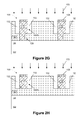
- FIGS. 2I-2J depict the product 100 after a conformal deposition process was performed to form a relatively thin (e.g., 2-5 nm) conformal etch stop layer 133 , e.g., silicon nitride, on the product 100 and particularly on the insulating material 106 and the conductive lines 126 .
- FIG. 2I is a cross-sectional view taken through both the conductive lines 126 and the vias 123
- FIG. 2J is a cross-sectional view taken through just the conductive lines 126 in a location where the conductive vias 123 are not formed.
- the etch stop layer 133 can be used as an etch stop in forming conductive structures in another metallization layer (not shown) that will be formed above the illustrative metallization layer depicted herein.
- FIGS. 2K-2L depict the product 100 after a layer of material 134 , i.e., a capping layer, was formed on the product 100 and after a CMP process was performed to planarize its upper surface.
- FIG. 2K is a cross-sectional view taken through both the conductive lines 126 and the vias 123
- FIG. 2L is a cross-sectional view taken through just the conductive lines 126 in a location where the conductive vias 123 are not formed.
- the capping layer of material 134 may be comprised of a material such as silicon nitride, and it may be formed to a thickness of about 10-30 nm.
- the lateral spacing 136 between the conductive lines 126 and the remaining portions of the non-damaged insulating material 106 is small enough (e.g., 0.5-5 nm) such that the capping layer of material 134 does not fill a substantial portion of that lateral space 136 . This results in the formation of air gaps 132 between the adjacent conductive lines 126 .
- the remaining portion 106 X of the undamaged insulating material 106 may have a lateral width on the order of about 2-10 nm. Thus, unlike the prior art process described in the background section of this application, some of the insulating material ( 106 X) remains positioned between the conductive lines 126 instead of simply being an open air space.
- the presence of the material 106 X reduces leakage between the adjacent conductive lines 126 .
- some undesirable damage of an underlying layer of insulating material may have occurred.
- efforts were made to “repair” the damaged insulating material by using SiCOH, SiCNH, CxHy, etc. based chemicals to form a thin film coating the damaged surface in an attempt to restore the dielectric constant and restore the film hydrophobicity, with or without UV assisted, plasma enhanced or atomic layer deposition.
Abstract
Description
Claims (19)
Priority Applications (1)
| Application Number | Priority Date | Filing Date | Title |
|---|---|---|---|
| US14/822,258 US9768058B2 (en) | 2015-08-10 | 2015-08-10 | Methods of forming air gaps in metallization layers on integrated circuit products |
Applications Claiming Priority (1)
| Application Number | Priority Date | Filing Date | Title |
|---|---|---|---|
| US14/822,258 US9768058B2 (en) | 2015-08-10 | 2015-08-10 | Methods of forming air gaps in metallization layers on integrated circuit products |
Publications (2)
| Publication Number | Publication Date |
|---|---|
| US20170047242A1 US20170047242A1 (en) | 2017-02-16 |
| US9768058B2 true US9768058B2 (en) | 2017-09-19 |
Family
ID=57996098
Family Applications (1)
| Application Number | Title | Priority Date | Filing Date |
|---|---|---|---|
| US14/822,258 Active US9768058B2 (en) | 2015-08-10 | 2015-08-10 | Methods of forming air gaps in metallization layers on integrated circuit products |
Country Status (1)
| Country | Link |
|---|---|
| US (1) | US9768058B2 (en) |
Cited By (1)
| Publication number | Priority date | Publication date | Assignee | Title |
|---|---|---|---|---|
| US20160372382A1 (en) * | 2015-06-16 | 2016-12-22 | Samsung Electronics Co., Ltd. | Semiconductor device and method of fabricating the same |
Families Citing this family (5)
| Publication number | Priority date | Publication date | Assignee | Title |
|---|---|---|---|---|
| US10388564B2 (en) | 2016-01-12 | 2019-08-20 | Micron Technology, Inc. | Method for fabricating a memory device having two contacts |
| US10043753B2 (en) * | 2016-12-13 | 2018-08-07 | Globalfoundries Inc. | Airgaps to isolate metallization features |
| KR20210049604A (en) * | 2019-10-25 | 2021-05-06 | 삼성전자주식회사 | Integrated circuit device and method of manufacturing the same |
| JP2021150341A (en) * | 2020-03-16 | 2021-09-27 | キオクシア株式会社 | Semiconductor device and manufacturing method for semiconductor device |
| US11769770B2 (en) * | 2021-05-06 | 2023-09-26 | Taiwan Semiconductor Manufacturing Company, Ltd. | Methods of forming a semiconductor device having an air spacer |
Citations (34)
| Publication number | Priority date | Publication date | Assignee | Title |
|---|---|---|---|---|
| US5869379A (en) | 1997-12-08 | 1999-02-09 | Advanced Micro Devices, Inc. | Method of forming air gap spacer for high performance MOSFETS' |
| US5949143A (en) | 1998-01-22 | 1999-09-07 | Advanced Micro Devices, Inc. | Semiconductor interconnect structure with air gap for reducing intralayer capacitance in metal layers in damascene metalization process |
| US5953625A (en) | 1997-12-15 | 1999-09-14 | Advanced Micro Devices, Inc. | Air voids underneath metal lines to reduce parasitic capacitance |
| US6160316A (en) | 1998-03-04 | 2000-12-12 | Advanced Micro Devices, Inc. | Integrated circuit utilizing an air gap to reduce capacitance between adjacent metal linewidths |
| US6312874B1 (en) | 1998-11-06 | 2001-11-06 | Advanced Micro Devices, Inc. | Method for forming a dual damascene trench and underlying borderless via in low dielectric constant materials |
| US6376330B1 (en) | 1996-06-05 | 2002-04-23 | Advanced Micro Devices, Inc. | Dielectric having an air gap formed between closely spaced interconnect lines |
| US20020158337A1 (en) | 2000-02-08 | 2002-10-31 | Babich Katherina E. | Multilayer interconnect structure containing air gaps and method for making |
| US6713835B1 (en) | 2003-05-22 | 2004-03-30 | International Business Machines Corporation | Method for manufacturing a multi-level interconnect structure |
| US6737725B2 (en) | 2000-08-31 | 2004-05-18 | International Business Machines Corporation | Multilevel interconnect structure containing air gaps and method for making |
| US20040213971A1 (en) | 2002-11-05 | 2004-10-28 | International Business Machines Corporation | Nonlithographic method to produce masks by selective reaction, articles produced, and composition for same |
| US20040232552A1 (en) | 2002-12-09 | 2004-11-25 | Advanced Micro Devices, Inc. | Air gap dual damascene process and structure |
| US6838354B2 (en) | 2002-12-20 | 2005-01-04 | Freescale Semiconductor, Inc. | Method for forming a passivation layer for air gap formation |
| US6838355B1 (en) | 2003-08-04 | 2005-01-04 | International Business Machines Corporation | Damascene interconnect structures including etchback for low-k dielectric materials |
| US20060073695A1 (en) | 2004-09-30 | 2006-04-06 | International Business Machines Corporation | Gas dielectric structure forming methods |
| US7026235B1 (en) | 2002-02-07 | 2006-04-11 | Cypress Semiconductor Corporation | Dual-damascene process and associated floating metal structures |
| US20060088975A1 (en) | 2004-10-25 | 2006-04-27 | Matsushita Electric Industrial Co., Ltd. | Method for fabricating semiconductor device and semiconductor device |
| US20060205623A1 (en) * | 2005-03-11 | 2006-09-14 | Kanto Kagaku Kabushiki Kaisha | Composition for photoresist stripping solution and process of photoresist stripping |
| US20070096319A1 (en) | 2005-11-03 | 2007-05-03 | International Business Machines Corporation | Method for fabricating and BEOL interconnect structures with simultaneous formation of high-k and low-k dielectric regions |
| US20070099417A1 (en) | 2005-10-28 | 2007-05-03 | Applied Materials, Inc. | Adhesion and minimizing oxidation on electroless CO alloy films for integration with low K inter-metal dielectric and etch stop |
| US20070178713A1 (en) | 2006-01-27 | 2007-08-02 | Jeng Shin-Puu | Method for forming a dielectric layer with an air gap, and a structure including the dielectric layer with the air gap |
| US20070259516A1 (en) | 2006-05-08 | 2007-11-08 | International Business Machines Corporation | Multilayer interconnect structure containing air gaps and method for making |
| US7319274B2 (en) | 2003-09-30 | 2008-01-15 | Interuniversitair Microelektronica Centrum (Imec V2W) | Methods for selective integration of airgaps and devices made by such methods |
| US20080073748A1 (en) | 2006-09-21 | 2008-03-27 | Bielefeld Jeffery D | Dielectric spacers for metal interconnects and method to form the same |
| US20080124917A1 (en) | 2006-11-23 | 2008-05-29 | Samsung Electronics Co., Ltd. | Method of manufacturing a semiconductor device having air gaps |
| US20080169542A1 (en) | 2005-08-17 | 2008-07-17 | Fujitsu Limited | Semiconductor device and manufacturing method thereof |
| US20080169565A1 (en) | 2007-01-11 | 2008-07-17 | International Business Machines Corporation | Metal capping process for beol interconnect with air gaps |
| US20090072409A1 (en) * | 2007-09-14 | 2009-03-19 | International Business Machines Corporation | Interconnect Structures Incorporating Air-Gap Spacers |
| DE102008044984A1 (en) | 2008-08-29 | 2010-07-15 | Advanced Micro Devices, Inc., Sunnyvale | Semiconductor device with stress relaxation columns for improving chip package interaction stability |
| US20100270683A1 (en) * | 2009-04-24 | 2010-10-28 | Nec Electronics Corporation | Semiconductor device and method of manufacturing semiconductor device |
| US7868455B2 (en) | 2007-11-01 | 2011-01-11 | Taiwan Semiconductor Manufacturing Company, Ltd. | Solving via-misalignment issues in interconnect structures having air-gaps |
| US8048796B2 (en) | 2009-05-29 | 2011-11-01 | Globalfoundries Inc. | Microstructure device including a metallization structure with self-aligned air gaps formed based on a sacrificial material |
| US8399335B2 (en) | 2010-06-30 | 2013-03-19 | GlobalFoundries, Inc. | Sophisticated metallization systems in semiconductors formed by removing damaged dielectric layers after forming the metal features |
| US8883610B2 (en) | 2008-11-28 | 2014-11-11 | Globalfoundries Inc. | Microstructure device including a metallization structure with self-aligned air gaps between closely spaced metal lines |
| US20150332999A1 (en) * | 2014-05-13 | 2015-11-19 | Taiwan Semiconductor Manufacturing Company Ltd. | Semiconductor interconnect structure and manufacturing method thereof |
-
2015
- 2015-08-10 US US14/822,258 patent/US9768058B2/en active Active
Patent Citations (36)
| Publication number | Priority date | Publication date | Assignee | Title |
|---|---|---|---|---|
| US6376330B1 (en) | 1996-06-05 | 2002-04-23 | Advanced Micro Devices, Inc. | Dielectric having an air gap formed between closely spaced interconnect lines |
| US5869379A (en) | 1997-12-08 | 1999-02-09 | Advanced Micro Devices, Inc. | Method of forming air gap spacer for high performance MOSFETS' |
| US5953625A (en) | 1997-12-15 | 1999-09-14 | Advanced Micro Devices, Inc. | Air voids underneath metal lines to reduce parasitic capacitance |
| US5949143A (en) | 1998-01-22 | 1999-09-07 | Advanced Micro Devices, Inc. | Semiconductor interconnect structure with air gap for reducing intralayer capacitance in metal layers in damascene metalization process |
| US6160316A (en) | 1998-03-04 | 2000-12-12 | Advanced Micro Devices, Inc. | Integrated circuit utilizing an air gap to reduce capacitance between adjacent metal linewidths |
| US6312874B1 (en) | 1998-11-06 | 2001-11-06 | Advanced Micro Devices, Inc. | Method for forming a dual damascene trench and underlying borderless via in low dielectric constant materials |
| US20050037604A1 (en) | 2000-02-08 | 2005-02-17 | International Business Machines Corporation | Multilayer interconnect structure containing air gaps and method for making |
| US20020158337A1 (en) | 2000-02-08 | 2002-10-31 | Babich Katherina E. | Multilayer interconnect structure containing air gaps and method for making |
| US6737725B2 (en) | 2000-08-31 | 2004-05-18 | International Business Machines Corporation | Multilevel interconnect structure containing air gaps and method for making |
| US7026235B1 (en) | 2002-02-07 | 2006-04-11 | Cypress Semiconductor Corporation | Dual-damascene process and associated floating metal structures |
| US20040213971A1 (en) | 2002-11-05 | 2004-10-28 | International Business Machines Corporation | Nonlithographic method to produce masks by selective reaction, articles produced, and composition for same |
| US20040232552A1 (en) | 2002-12-09 | 2004-11-25 | Advanced Micro Devices, Inc. | Air gap dual damascene process and structure |
| US6838354B2 (en) | 2002-12-20 | 2005-01-04 | Freescale Semiconductor, Inc. | Method for forming a passivation layer for air gap formation |
| US6713835B1 (en) | 2003-05-22 | 2004-03-30 | International Business Machines Corporation | Method for manufacturing a multi-level interconnect structure |
| US6838355B1 (en) | 2003-08-04 | 2005-01-04 | International Business Machines Corporation | Damascene interconnect structures including etchback for low-k dielectric materials |
| US7319274B2 (en) | 2003-09-30 | 2008-01-15 | Interuniversitair Microelektronica Centrum (Imec V2W) | Methods for selective integration of airgaps and devices made by such methods |
| US20060073695A1 (en) | 2004-09-30 | 2006-04-06 | International Business Machines Corporation | Gas dielectric structure forming methods |
| US20060088975A1 (en) | 2004-10-25 | 2006-04-27 | Matsushita Electric Industrial Co., Ltd. | Method for fabricating semiconductor device and semiconductor device |
| US20060205623A1 (en) * | 2005-03-11 | 2006-09-14 | Kanto Kagaku Kabushiki Kaisha | Composition for photoresist stripping solution and process of photoresist stripping |
| US20080169542A1 (en) | 2005-08-17 | 2008-07-17 | Fujitsu Limited | Semiconductor device and manufacturing method thereof |
| US20070099417A1 (en) | 2005-10-28 | 2007-05-03 | Applied Materials, Inc. | Adhesion and minimizing oxidation on electroless CO alloy films for integration with low K inter-metal dielectric and etch stop |
| US20070096319A1 (en) | 2005-11-03 | 2007-05-03 | International Business Machines Corporation | Method for fabricating and BEOL interconnect structures with simultaneous formation of high-k and low-k dielectric regions |
| US20070178713A1 (en) | 2006-01-27 | 2007-08-02 | Jeng Shin-Puu | Method for forming a dielectric layer with an air gap, and a structure including the dielectric layer with the air gap |
| US20070259516A1 (en) | 2006-05-08 | 2007-11-08 | International Business Machines Corporation | Multilayer interconnect structure containing air gaps and method for making |
| DE112007002215T5 (en) | 2006-09-21 | 2009-07-30 | Intel Corporation, Santa Clara | Dielectric spacers for metal joints and process for their preparation |
| US20080073748A1 (en) | 2006-09-21 | 2008-03-27 | Bielefeld Jeffery D | Dielectric spacers for metal interconnects and method to form the same |
| US20080124917A1 (en) | 2006-11-23 | 2008-05-29 | Samsung Electronics Co., Ltd. | Method of manufacturing a semiconductor device having air gaps |
| US20080169565A1 (en) | 2007-01-11 | 2008-07-17 | International Business Machines Corporation | Metal capping process for beol interconnect with air gaps |
| US20090072409A1 (en) * | 2007-09-14 | 2009-03-19 | International Business Machines Corporation | Interconnect Structures Incorporating Air-Gap Spacers |
| US7868455B2 (en) | 2007-11-01 | 2011-01-11 | Taiwan Semiconductor Manufacturing Company, Ltd. | Solving via-misalignment issues in interconnect structures having air-gaps |
| DE102008044984A1 (en) | 2008-08-29 | 2010-07-15 | Advanced Micro Devices, Inc., Sunnyvale | Semiconductor device with stress relaxation columns for improving chip package interaction stability |
| US8883610B2 (en) | 2008-11-28 | 2014-11-11 | Globalfoundries Inc. | Microstructure device including a metallization structure with self-aligned air gaps between closely spaced metal lines |
| US20100270683A1 (en) * | 2009-04-24 | 2010-10-28 | Nec Electronics Corporation | Semiconductor device and method of manufacturing semiconductor device |
| US8048796B2 (en) | 2009-05-29 | 2011-11-01 | Globalfoundries Inc. | Microstructure device including a metallization structure with self-aligned air gaps formed based on a sacrificial material |
| US8399335B2 (en) | 2010-06-30 | 2013-03-19 | GlobalFoundries, Inc. | Sophisticated metallization systems in semiconductors formed by removing damaged dielectric layers after forming the metal features |
| US20150332999A1 (en) * | 2014-05-13 | 2015-11-19 | Taiwan Semiconductor Manufacturing Company Ltd. | Semiconductor interconnect structure and manufacturing method thereof |
Non-Patent Citations (5)
| Title |
|---|
| Lee and Graves, "The effect of VUV radiation from Ar/O2 plasmas on low-k SiOCH films," J. Phys. D: Appl. Phys., 44:325203, 2011. |
| Translation of Official Communication from German Patent Office for German Patent Application No. 10 2008 059 650.7 dated Nov. 11, 2010. |
| Translation of Official Communication from German Patent Office for German Patent Application No. 10 2008 059 650.7 dated Sep. 25, 2009. |
| Translation of Official Communication from German Patent Office for German Patent Application No. 10 2009 023 377.6 dated Oct. 5, 2010. |
| Translation of Official Communication from German Patent Office for German Patent Application No. 10 2010 030 757.2 dated Feb. 18, 2011. |
Cited By (1)
| Publication number | Priority date | Publication date | Assignee | Title |
|---|---|---|---|---|
| US20160372382A1 (en) * | 2015-06-16 | 2016-12-22 | Samsung Electronics Co., Ltd. | Semiconductor device and method of fabricating the same |
Also Published As
| Publication number | Publication date |
|---|---|
| US20170047242A1 (en) | 2017-02-16 |
Similar Documents
| Publication | Publication Date | Title |
|---|---|---|
| US9553028B2 (en) | Methods of forming reduced resistance local interconnect structures and the resulting devices | |
| US9768058B2 (en) | Methods of forming air gaps in metallization layers on integrated circuit products | |
| US10249726B2 (en) | Methods of forming a protection layer on a semiconductor device and the resulting device | |
| US9312182B2 (en) | Forming gate and source/drain contact openings by performing a common etch patterning process | |
| US8791013B2 (en) | Pattern forming method | |
| US9397045B2 (en) | Structure and formation method of damascene structure | |
| US20160372413A1 (en) | Unique bi-layer etch stop to protect conductive structures during a metal hard mask removal process and methods of using same | |
| US9899321B1 (en) | Methods of forming a gate contact for a semiconductor device above the active region | |
| US20160133623A1 (en) | Methods of forming a combined gate and source/drain contact structure and the resulting device | |
| US9607882B2 (en) | Semiconductor device and manufacturing method thereof | |
| US8580684B2 (en) | Contact elements of semiconductor devices comprising a continuous transition to metal lines of a metallization layer | |
| US20170004999A1 (en) | Self-aligned via process flow | |
| US8669176B1 (en) | BEOL integration scheme for copper CMP to prevent dendrite formation | |
| US6555892B2 (en) | Semiconductor device with reduced line-to-line capacitance and cross talk noise | |
| US10438893B2 (en) | Metal interconnect structure and method for fabricating the same | |
| US10504790B2 (en) | Methods of forming conductive spacers for gate contacts and the resulting device | |
| US9406883B1 (en) | Structure and formation method of memory device | |
| US9870994B2 (en) | Semiconductor device and method for fabricating the same | |
| US9947589B1 (en) | Methods of forming a gate contact for a transistor above an active region and the resulting device | |
| US20140357078A1 (en) | Methods of forming conductive structures using a sacrificial material during an etching process that is performed to remove a metal hard mask | |
| US8673770B2 (en) | Methods of forming conductive structures in dielectric layers on an integrated circuit device | |
| US11699589B2 (en) | Method for forming patterned mask layer | |
| US8889549B2 (en) | Methods of forming conductive structures using a sacrificial liner layer | |
| US8883631B1 (en) | Methods of forming conductive structures using a sacrificial material during a metal hard mask removal process | |
| WO2002041405A1 (en) | Semiconductor device with reduced line-to-line capacitance and cross talk noise |
Legal Events
| Date | Code | Title | Description |
|---|---|---|---|
| AS | Assignment |
Owner name: GLOBALFOUNDRIES INC., CAYMAN ISLANDS Free format text: ASSIGNMENT OF ASSIGNORS INTEREST;ASSIGNORS:SUN, ZHIGUO;FANG, QIANG;WITT, CHRISTIAN;REEL/FRAME:036316/0207 Effective date: 20150805 |
|
| STCF | Information on status: patent grant |
Free format text: PATENTED CASE |
|
| AS | Assignment |
Owner name: WILMINGTON TRUST, NATIONAL ASSOCIATION, DELAWARE Free format text: SECURITY AGREEMENT;ASSIGNOR:GLOBALFOUNDRIES INC.;REEL/FRAME:049490/0001 Effective date: 20181127 |
|
| MAFP | Maintenance fee payment |
Free format text: PAYMENT OF MAINTENANCE FEE, 4TH YEAR, LARGE ENTITY (ORIGINAL EVENT CODE: M1551); ENTITY STATUS OF PATENT OWNER: LARGE ENTITY Year of fee payment: 4 |
|
| AS | Assignment |
Owner name: GLOBALFOUNDRIES U.S. INC., CALIFORNIA Free format text: ASSIGNMENT OF ASSIGNORS INTEREST;ASSIGNOR:GLOBALFOUNDRIES INC.;REEL/FRAME:054633/0001 Effective date: 20201022 |
|
| AS | Assignment |
Owner name: GLOBALFOUNDRIES INC., CAYMAN ISLANDS Free format text: RELEASE BY SECURED PARTY;ASSIGNOR:WILMINGTON TRUST, NATIONAL ASSOCIATION;REEL/FRAME:054636/0001 Effective date: 20201117 |
|
| AS | Assignment |
Owner name: GLOBALFOUNDRIES U.S. INC., NEW YORK Free format text: RELEASE BY SECURED PARTY;ASSIGNOR:WILMINGTON TRUST, NATIONAL ASSOCIATION;REEL/FRAME:056987/0001 Effective date: 20201117 |