US9761581B1 - Single mask level including a resistor and a through-gate implant - Google Patents
Single mask level including a resistor and a through-gate implant Download PDFInfo
- Publication number
- US9761581B1 US9761581B1 US15/060,261 US201615060261A US9761581B1 US 9761581 B1 US9761581 B1 US 9761581B1 US 201615060261 A US201615060261 A US 201615060261A US 9761581 B1 US9761581 B1 US 9761581B1
- Authority
- US
- United States
- Prior art keywords
- polysilicon
- area
- resistor
- implant
- bsd
- Prior art date
- Legal status (The legal status is an assumption and is not a legal conclusion. Google has not performed a legal analysis and makes no representation as to the accuracy of the status listed.)
- Active
Links
- 239000007943 implant Substances 0.000 title claims abstract description 78
- 229910021420 polycrystalline silicon Inorganic materials 0.000 claims abstract description 96
- 229920005591 polysilicon Polymers 0.000 claims abstract description 96
- 239000010410 layer Substances 0.000 claims abstract description 46
- 238000000034 method Methods 0.000 claims abstract description 44
- 239000004065 semiconductor Substances 0.000 claims abstract description 27
- 239000002344 surface layer Substances 0.000 claims abstract description 21
- 239000002019 doping agent Substances 0.000 claims description 19
- ZOXJGFHDIHLPTG-UHFFFAOYSA-N Boron Chemical compound [B] ZOXJGFHDIHLPTG-UHFFFAOYSA-N 0.000 claims description 16
- 229910052796 boron Inorganic materials 0.000 claims description 16
- 239000003990 capacitor Substances 0.000 claims description 10
- 238000002955 isolation Methods 0.000 claims description 9
- 229910052751 metal Inorganic materials 0.000 claims description 7
- 239000002184 metal Substances 0.000 claims description 7
- 230000000873 masking effect Effects 0.000 claims description 6
- 238000000059 patterning Methods 0.000 claims description 6
- 239000000758 substrate Substances 0.000 claims description 5
- 238000000151 deposition Methods 0.000 claims description 4
- 239000000463 material Substances 0.000 description 17
- 238000005516 engineering process Methods 0.000 description 10
- 150000002500 ions Chemical class 0.000 description 7
- XUIMIQQOPSSXEZ-UHFFFAOYSA-N Silicon Chemical compound [Si] XUIMIQQOPSSXEZ-UHFFFAOYSA-N 0.000 description 5
- 229910052710 silicon Inorganic materials 0.000 description 5
- 239000010703 silicon Substances 0.000 description 5
- OAICVXFJPJFONN-UHFFFAOYSA-N Phosphorus Chemical compound [P] OAICVXFJPJFONN-UHFFFAOYSA-N 0.000 description 4
- 238000005530 etching Methods 0.000 description 4
- 229910052698 phosphorus Inorganic materials 0.000 description 4
- 239000011574 phosphorus Substances 0.000 description 4
- 229910021332 silicide Inorganic materials 0.000 description 4
- FVBUAEGBCNSCDD-UHFFFAOYSA-N silicide(4-) Chemical compound [Si-4] FVBUAEGBCNSCDD-UHFFFAOYSA-N 0.000 description 4
- BHEPBYXIRTUNPN-UHFFFAOYSA-N hydridophosphorus(.) (triplet) Chemical compound [PH] BHEPBYXIRTUNPN-UHFFFAOYSA-N 0.000 description 3
- IJGRMHOSHXDMSA-UHFFFAOYSA-N Atomic nitrogen Chemical compound N#N IJGRMHOSHXDMSA-UHFFFAOYSA-N 0.000 description 2
- 238000007792 addition Methods 0.000 description 2
- 230000015572 biosynthetic process Effects 0.000 description 2
- 230000008021 deposition Effects 0.000 description 2
- 238000009792 diffusion process Methods 0.000 description 2
- 238000001465 metallisation Methods 0.000 description 2
- ALKWEXBKAHPJAQ-NAKRPEOUSA-N Asn-Leu-Asp-Asp Chemical group NC(=O)C[C@H](N)C(=O)N[C@@H](CC(C)C)C(=O)N[C@@H](CC(O)=O)C(=O)N[C@@H](CC(O)=O)C(O)=O ALKWEXBKAHPJAQ-NAKRPEOUSA-N 0.000 description 1
- PXGOKWXKJXAPGV-UHFFFAOYSA-N Fluorine Chemical compound FF PXGOKWXKJXAPGV-UHFFFAOYSA-N 0.000 description 1
- 229910052581 Si3N4 Inorganic materials 0.000 description 1
- VYPSYNLAJGMNEJ-UHFFFAOYSA-N Silicium dioxide Chemical compound O=[Si]=O VYPSYNLAJGMNEJ-UHFFFAOYSA-N 0.000 description 1
- 229910000577 Silicon-germanium Inorganic materials 0.000 description 1
- LEVVHYCKPQWKOP-UHFFFAOYSA-N [Si].[Ge] Chemical compound [Si].[Ge] LEVVHYCKPQWKOP-UHFFFAOYSA-N 0.000 description 1
- 229910052785 arsenic Inorganic materials 0.000 description 1
- 230000004888 barrier function Effects 0.000 description 1
- 230000001010 compromised effect Effects 0.000 description 1
- 230000007547 defect Effects 0.000 description 1
- 238000012217 deletion Methods 0.000 description 1
- 230000037430 deletion Effects 0.000 description 1
- 230000005669 field effect Effects 0.000 description 1
- 229910052731 fluorine Inorganic materials 0.000 description 1
- 239000011737 fluorine Substances 0.000 description 1
- 229910052732 germanium Inorganic materials 0.000 description 1
- GNPVGFCGXDBREM-UHFFFAOYSA-N germanium atom Chemical compound [Ge] GNPVGFCGXDBREM-UHFFFAOYSA-N 0.000 description 1
- 238000002513 implantation Methods 0.000 description 1
- 238000012986 modification Methods 0.000 description 1
- 230000004048 modification Effects 0.000 description 1
- 229910052757 nitrogen Inorganic materials 0.000 description 1
- 230000003647 oxidation Effects 0.000 description 1
- 238000007254 oxidation reaction Methods 0.000 description 1
- 238000012856 packing Methods 0.000 description 1
- 238000002161 passivation Methods 0.000 description 1
- 230000000149 penetrating effect Effects 0.000 description 1
- 229920002120 photoresistant polymer Polymers 0.000 description 1
- 238000012545 processing Methods 0.000 description 1
- HQVNEWCFYHHQES-UHFFFAOYSA-N silicon nitride Chemical compound N12[Si]34N5[Si]62N3[Si]51N64 HQVNEWCFYHHQES-UHFFFAOYSA-N 0.000 description 1
- 229910052814 silicon oxide Inorganic materials 0.000 description 1
- 238000006467 substitution reaction Methods 0.000 description 1
Images


Classifications
-
- H—ELECTRICITY
- H01—ELECTRIC ELEMENTS
- H01L—SEMICONDUCTOR DEVICES NOT COVERED BY CLASS H10
- H01L27/00—Devices consisting of a plurality of semiconductor or other solid-state components formed in or on a common substrate
- H01L27/02—Devices consisting of a plurality of semiconductor or other solid-state components formed in or on a common substrate including semiconductor components specially adapted for rectifying, oscillating, amplifying or switching and having at least one potential-jump barrier or surface barrier; including integrated passive circuit elements with at least one potential-jump barrier or surface barrier
- H01L27/04—Devices consisting of a plurality of semiconductor or other solid-state components formed in or on a common substrate including semiconductor components specially adapted for rectifying, oscillating, amplifying or switching and having at least one potential-jump barrier or surface barrier; including integrated passive circuit elements with at least one potential-jump barrier or surface barrier the substrate being a semiconductor body
- H01L27/06—Devices consisting of a plurality of semiconductor or other solid-state components formed in or on a common substrate including semiconductor components specially adapted for rectifying, oscillating, amplifying or switching and having at least one potential-jump barrier or surface barrier; including integrated passive circuit elements with at least one potential-jump barrier or surface barrier the substrate being a semiconductor body including a plurality of individual components in a non-repetitive configuration
- H01L27/0611—Devices consisting of a plurality of semiconductor or other solid-state components formed in or on a common substrate including semiconductor components specially adapted for rectifying, oscillating, amplifying or switching and having at least one potential-jump barrier or surface barrier; including integrated passive circuit elements with at least one potential-jump barrier or surface barrier the substrate being a semiconductor body including a plurality of individual components in a non-repetitive configuration integrated circuits having a two-dimensional layout of components without a common active region
- H01L27/0617—Devices consisting of a plurality of semiconductor or other solid-state components formed in or on a common substrate including semiconductor components specially adapted for rectifying, oscillating, amplifying or switching and having at least one potential-jump barrier or surface barrier; including integrated passive circuit elements with at least one potential-jump barrier or surface barrier the substrate being a semiconductor body including a plurality of individual components in a non-repetitive configuration integrated circuits having a two-dimensional layout of components without a common active region comprising components of the field-effect type
- H01L27/0635—Devices consisting of a plurality of semiconductor or other solid-state components formed in or on a common substrate including semiconductor components specially adapted for rectifying, oscillating, amplifying or switching and having at least one potential-jump barrier or surface barrier; including integrated passive circuit elements with at least one potential-jump barrier or surface barrier the substrate being a semiconductor body including a plurality of individual components in a non-repetitive configuration integrated circuits having a two-dimensional layout of components without a common active region comprising components of the field-effect type in combination with bipolar transistors and diodes, or resistors, or capacitors
-
- H—ELECTRICITY
- H01—ELECTRIC ELEMENTS
- H01L—SEMICONDUCTOR DEVICES NOT COVERED BY CLASS H10
- H01L21/00—Processes or apparatus adapted for the manufacture or treatment of semiconductor or solid state devices or of parts thereof
- H01L21/02—Manufacture or treatment of semiconductor devices or of parts thereof
- H01L21/04—Manufacture or treatment of semiconductor devices or of parts thereof the devices having at least one potential-jump barrier or surface barrier, e.g. PN junction, depletion layer or carrier concentration layer
- H01L21/18—Manufacture or treatment of semiconductor devices or of parts thereof the devices having at least one potential-jump barrier or surface barrier, e.g. PN junction, depletion layer or carrier concentration layer the devices having semiconductor bodies comprising elements of Group IV of the Periodic System or AIIIBV compounds with or without impurities, e.g. doping materials
- H01L21/26—Bombardment with radiation
- H01L21/263—Bombardment with radiation with high-energy radiation
- H01L21/265—Bombardment with radiation with high-energy radiation producing ion implantation
- H01L21/26506—Bombardment with radiation with high-energy radiation producing ion implantation in group IV semiconductors
- H01L21/26513—Bombardment with radiation with high-energy radiation producing ion implantation in group IV semiconductors of electrically active species
-
- H—ELECTRICITY
- H01—ELECTRIC ELEMENTS
- H01L—SEMICONDUCTOR DEVICES NOT COVERED BY CLASS H10
- H01L21/00—Processes or apparatus adapted for the manufacture or treatment of semiconductor or solid state devices or of parts thereof
- H01L21/02—Manufacture or treatment of semiconductor devices or of parts thereof
- H01L21/04—Manufacture or treatment of semiconductor devices or of parts thereof the devices having at least one potential-jump barrier or surface barrier, e.g. PN junction, depletion layer or carrier concentration layer
- H01L21/18—Manufacture or treatment of semiconductor devices or of parts thereof the devices having at least one potential-jump barrier or surface barrier, e.g. PN junction, depletion layer or carrier concentration layer the devices having semiconductor bodies comprising elements of Group IV of the Periodic System or AIIIBV compounds with or without impurities, e.g. doping materials
- H01L21/26—Bombardment with radiation
- H01L21/263—Bombardment with radiation with high-energy radiation
- H01L21/265—Bombardment with radiation with high-energy radiation producing ion implantation
- H01L21/266—Bombardment with radiation with high-energy radiation producing ion implantation using masks
-
- H—ELECTRICITY
- H01—ELECTRIC ELEMENTS
- H01L—SEMICONDUCTOR DEVICES NOT COVERED BY CLASS H10
- H01L21/00—Processes or apparatus adapted for the manufacture or treatment of semiconductor or solid state devices or of parts thereof
- H01L21/02—Manufacture or treatment of semiconductor devices or of parts thereof
- H01L21/04—Manufacture or treatment of semiconductor devices or of parts thereof the devices having at least one potential-jump barrier or surface barrier, e.g. PN junction, depletion layer or carrier concentration layer
- H01L21/18—Manufacture or treatment of semiconductor devices or of parts thereof the devices having at least one potential-jump barrier or surface barrier, e.g. PN junction, depletion layer or carrier concentration layer the devices having semiconductor bodies comprising elements of Group IV of the Periodic System or AIIIBV compounds with or without impurities, e.g. doping materials
- H01L21/28—Manufacture of electrodes on semiconductor bodies using processes or apparatus not provided for in groups H01L21/20 - H01L21/268
- H01L21/28008—Making conductor-insulator-semiconductor electrodes
- H01L21/28017—Making conductor-insulator-semiconductor electrodes the insulator being formed after the semiconductor body, the semiconductor being silicon
- H01L21/28026—Making conductor-insulator-semiconductor electrodes the insulator being formed after the semiconductor body, the semiconductor being silicon characterised by the conductor
- H01L21/28035—Making conductor-insulator-semiconductor electrodes the insulator being formed after the semiconductor body, the semiconductor being silicon characterised by the conductor the final conductor layer next to the insulator being silicon, e.g. polysilicon, with or without impurities
-
- H—ELECTRICITY
- H01—ELECTRIC ELEMENTS
- H01L—SEMICONDUCTOR DEVICES NOT COVERED BY CLASS H10
- H01L21/00—Processes or apparatus adapted for the manufacture or treatment of semiconductor or solid state devices or of parts thereof
- H01L21/02—Manufacture or treatment of semiconductor devices or of parts thereof
- H01L21/04—Manufacture or treatment of semiconductor devices or of parts thereof the devices having at least one potential-jump barrier or surface barrier, e.g. PN junction, depletion layer or carrier concentration layer
- H01L21/18—Manufacture or treatment of semiconductor devices or of parts thereof the devices having at least one potential-jump barrier or surface barrier, e.g. PN junction, depletion layer or carrier concentration layer the devices having semiconductor bodies comprising elements of Group IV of the Periodic System or AIIIBV compounds with or without impurities, e.g. doping materials
- H01L21/30—Treatment of semiconductor bodies using processes or apparatus not provided for in groups H01L21/20 - H01L21/26
- H01L21/31—Treatment of semiconductor bodies using processes or apparatus not provided for in groups H01L21/20 - H01L21/26 to form insulating layers thereon, e.g. for masking or by using photolithographic techniques; After treatment of these layers; Selection of materials for these layers
- H01L21/3205—Deposition of non-insulating-, e.g. conductive- or resistive-, layers on insulating layers; After-treatment of these layers
- H01L21/321—After treatment
- H01L21/3215—Doping the layers
- H01L21/32155—Doping polycristalline - or amorphous silicon layers
-
- H—ELECTRICITY
- H01—ELECTRIC ELEMENTS
- H01L—SEMICONDUCTOR DEVICES NOT COVERED BY CLASS H10
- H01L21/00—Processes or apparatus adapted for the manufacture or treatment of semiconductor or solid state devices or of parts thereof
- H01L21/70—Manufacture or treatment of devices consisting of a plurality of solid state components formed in or on a common substrate or of parts thereof; Manufacture of integrated circuit devices or of parts thereof
- H01L21/77—Manufacture or treatment of devices consisting of a plurality of solid state components or integrated circuits formed in, or on, a common substrate
- H01L21/78—Manufacture or treatment of devices consisting of a plurality of solid state components or integrated circuits formed in, or on, a common substrate with subsequent division of the substrate into plural individual devices
- H01L21/82—Manufacture or treatment of devices consisting of a plurality of solid state components or integrated circuits formed in, or on, a common substrate with subsequent division of the substrate into plural individual devices to produce devices, e.g. integrated circuits, each consisting of a plurality of components
- H01L21/822—Manufacture or treatment of devices consisting of a plurality of solid state components or integrated circuits formed in, or on, a common substrate with subsequent division of the substrate into plural individual devices to produce devices, e.g. integrated circuits, each consisting of a plurality of components the substrate being a semiconductor, using silicon technology
- H01L21/8232—Field-effect technology
- H01L21/8234—MIS technology, i.e. integration processes of field effect transistors of the conductor-insulator-semiconductor type
- H01L21/8238—Complementary field-effect transistors, e.g. CMOS
-
- H—ELECTRICITY
- H01—ELECTRIC ELEMENTS
- H01L—SEMICONDUCTOR DEVICES NOT COVERED BY CLASS H10
- H01L21/00—Processes or apparatus adapted for the manufacture or treatment of semiconductor or solid state devices or of parts thereof
- H01L21/70—Manufacture or treatment of devices consisting of a plurality of solid state components formed in or on a common substrate or of parts thereof; Manufacture of integrated circuit devices or of parts thereof
- H01L21/77—Manufacture or treatment of devices consisting of a plurality of solid state components or integrated circuits formed in, or on, a common substrate
- H01L21/78—Manufacture or treatment of devices consisting of a plurality of solid state components or integrated circuits formed in, or on, a common substrate with subsequent division of the substrate into plural individual devices
- H01L21/82—Manufacture or treatment of devices consisting of a plurality of solid state components or integrated circuits formed in, or on, a common substrate with subsequent division of the substrate into plural individual devices to produce devices, e.g. integrated circuits, each consisting of a plurality of components
- H01L21/822—Manufacture or treatment of devices consisting of a plurality of solid state components or integrated circuits formed in, or on, a common substrate with subsequent division of the substrate into plural individual devices to produce devices, e.g. integrated circuits, each consisting of a plurality of components the substrate being a semiconductor, using silicon technology
- H01L21/8248—Combination of bipolar and field-effect technology
- H01L21/8249—Bipolar and MOS technology
-
- H—ELECTRICITY
- H01—ELECTRIC ELEMENTS
- H01L—SEMICONDUCTOR DEVICES NOT COVERED BY CLASS H10
- H01L27/00—Devices consisting of a plurality of semiconductor or other solid-state components formed in or on a common substrate
- H01L27/02—Devices consisting of a plurality of semiconductor or other solid-state components formed in or on a common substrate including semiconductor components specially adapted for rectifying, oscillating, amplifying or switching and having at least one potential-jump barrier or surface barrier; including integrated passive circuit elements with at least one potential-jump barrier or surface barrier
- H01L27/04—Devices consisting of a plurality of semiconductor or other solid-state components formed in or on a common substrate including semiconductor components specially adapted for rectifying, oscillating, amplifying or switching and having at least one potential-jump barrier or surface barrier; including integrated passive circuit elements with at least one potential-jump barrier or surface barrier the substrate being a semiconductor body
- H01L27/06—Devices consisting of a plurality of semiconductor or other solid-state components formed in or on a common substrate including semiconductor components specially adapted for rectifying, oscillating, amplifying or switching and having at least one potential-jump barrier or surface barrier; including integrated passive circuit elements with at least one potential-jump barrier or surface barrier the substrate being a semiconductor body including a plurality of individual components in a non-repetitive configuration
- H01L27/0611—Devices consisting of a plurality of semiconductor or other solid-state components formed in or on a common substrate including semiconductor components specially adapted for rectifying, oscillating, amplifying or switching and having at least one potential-jump barrier or surface barrier; including integrated passive circuit elements with at least one potential-jump barrier or surface barrier the substrate being a semiconductor body including a plurality of individual components in a non-repetitive configuration integrated circuits having a two-dimensional layout of components without a common active region
- H01L27/0617—Devices consisting of a plurality of semiconductor or other solid-state components formed in or on a common substrate including semiconductor components specially adapted for rectifying, oscillating, amplifying or switching and having at least one potential-jump barrier or surface barrier; including integrated passive circuit elements with at least one potential-jump barrier or surface barrier the substrate being a semiconductor body including a plurality of individual components in a non-repetitive configuration integrated circuits having a two-dimensional layout of components without a common active region comprising components of the field-effect type
- H01L27/0629—Devices consisting of a plurality of semiconductor or other solid-state components formed in or on a common substrate including semiconductor components specially adapted for rectifying, oscillating, amplifying or switching and having at least one potential-jump barrier or surface barrier; including integrated passive circuit elements with at least one potential-jump barrier or surface barrier the substrate being a semiconductor body including a plurality of individual components in a non-repetitive configuration integrated circuits having a two-dimensional layout of components without a common active region comprising components of the field-effect type in combination with diodes, or resistors, or capacitors
-
- H—ELECTRICITY
- H01—ELECTRIC ELEMENTS
- H01L—SEMICONDUCTOR DEVICES NOT COVERED BY CLASS H10
- H01L27/00—Devices consisting of a plurality of semiconductor or other solid-state components formed in or on a common substrate
- H01L27/02—Devices consisting of a plurality of semiconductor or other solid-state components formed in or on a common substrate including semiconductor components specially adapted for rectifying, oscillating, amplifying or switching and having at least one potential-jump barrier or surface barrier; including integrated passive circuit elements with at least one potential-jump barrier or surface barrier
- H01L27/04—Devices consisting of a plurality of semiconductor or other solid-state components formed in or on a common substrate including semiconductor components specially adapted for rectifying, oscillating, amplifying or switching and having at least one potential-jump barrier or surface barrier; including integrated passive circuit elements with at least one potential-jump barrier or surface barrier the substrate being a semiconductor body
- H01L27/08—Devices consisting of a plurality of semiconductor or other solid-state components formed in or on a common substrate including semiconductor components specially adapted for rectifying, oscillating, amplifying or switching and having at least one potential-jump barrier or surface barrier; including integrated passive circuit elements with at least one potential-jump barrier or surface barrier the substrate being a semiconductor body including only semiconductor components of a single kind
- H01L27/085—Devices consisting of a plurality of semiconductor or other solid-state components formed in or on a common substrate including semiconductor components specially adapted for rectifying, oscillating, amplifying or switching and having at least one potential-jump barrier or surface barrier; including integrated passive circuit elements with at least one potential-jump barrier or surface barrier the substrate being a semiconductor body including only semiconductor components of a single kind including field-effect components only
- H01L27/088—Devices consisting of a plurality of semiconductor or other solid-state components formed in or on a common substrate including semiconductor components specially adapted for rectifying, oscillating, amplifying or switching and having at least one potential-jump barrier or surface barrier; including integrated passive circuit elements with at least one potential-jump barrier or surface barrier the substrate being a semiconductor body including only semiconductor components of a single kind including field-effect components only the components being field-effect transistors with insulated gate
- H01L27/092—Devices consisting of a plurality of semiconductor or other solid-state components formed in or on a common substrate including semiconductor components specially adapted for rectifying, oscillating, amplifying or switching and having at least one potential-jump barrier or surface barrier; including integrated passive circuit elements with at least one potential-jump barrier or surface barrier the substrate being a semiconductor body including only semiconductor components of a single kind including field-effect components only the components being field-effect transistors with insulated gate complementary MIS field-effect transistors
- H01L27/0922—Combination of complementary transistors having a different structure, e.g. stacked CMOS, high-voltage and low-voltage CMOS
-
- H—ELECTRICITY
- H01—ELECTRIC ELEMENTS
- H01L—SEMICONDUCTOR DEVICES NOT COVERED BY CLASS H10
- H01L28/00—Passive two-terminal components without a potential-jump or surface barrier for integrated circuits; Details thereof; Multistep manufacturing processes therefor
- H01L28/20—Resistors
-
- H—ELECTRICITY
- H01—ELECTRIC ELEMENTS
- H01L—SEMICONDUCTOR DEVICES NOT COVERED BY CLASS H10
- H01L28/00—Passive two-terminal components without a potential-jump or surface barrier for integrated circuits; Details thereof; Multistep manufacturing processes therefor
- H01L28/40—Capacitors
- H01L28/60—Electrodes
-
- H—ELECTRICITY
- H01—ELECTRIC ELEMENTS
- H01L—SEMICONDUCTOR DEVICES NOT COVERED BY CLASS H10
- H01L29/00—Semiconductor devices adapted for rectifying, amplifying, oscillating or switching, or capacitors or resistors with at least one potential-jump barrier or surface barrier, e.g. PN junction depletion layer or carrier concentration layer; Details of semiconductor bodies or of electrodes thereof ; Multistep manufacturing processes therefor
- H01L29/02—Semiconductor bodies ; Multistep manufacturing processes therefor
- H01L29/06—Semiconductor bodies ; Multistep manufacturing processes therefor characterised by their shape; characterised by the shapes, relative sizes, or dispositions of the semiconductor regions ; characterised by the concentration or distribution of impurities within semiconductor regions
- H01L29/0603—Semiconductor bodies ; Multistep manufacturing processes therefor characterised by their shape; characterised by the shapes, relative sizes, or dispositions of the semiconductor regions ; characterised by the concentration or distribution of impurities within semiconductor regions characterised by particular constructional design considerations, e.g. for preventing surface leakage, for controlling electric field concentration or for internal isolations regions
- H01L29/0642—Isolation within the component, i.e. internal isolation
- H01L29/0649—Dielectric regions, e.g. SiO2 regions, air gaps
-
- H—ELECTRICITY
- H01—ELECTRIC ELEMENTS
- H01L—SEMICONDUCTOR DEVICES NOT COVERED BY CLASS H10
- H01L29/00—Semiconductor devices adapted for rectifying, amplifying, oscillating or switching, or capacitors or resistors with at least one potential-jump barrier or surface barrier, e.g. PN junction depletion layer or carrier concentration layer; Details of semiconductor bodies or of electrodes thereof ; Multistep manufacturing processes therefor
- H01L29/02—Semiconductor bodies ; Multistep manufacturing processes therefor
- H01L29/06—Semiconductor bodies ; Multistep manufacturing processes therefor characterised by their shape; characterised by the shapes, relative sizes, or dispositions of the semiconductor regions ; characterised by the concentration or distribution of impurities within semiconductor regions
- H01L29/08—Semiconductor bodies ; Multistep manufacturing processes therefor characterised by their shape; characterised by the shapes, relative sizes, or dispositions of the semiconductor regions ; characterised by the concentration or distribution of impurities within semiconductor regions with semiconductor regions connected to an electrode carrying current to be rectified, amplified or switched and such electrode being part of a semiconductor device which comprises three or more electrodes
- H01L29/0804—Emitter regions of bipolar transistors
-
- H—ELECTRICITY
- H01—ELECTRIC ELEMENTS
- H01L—SEMICONDUCTOR DEVICES NOT COVERED BY CLASS H10
- H01L29/00—Semiconductor devices adapted for rectifying, amplifying, oscillating or switching, or capacitors or resistors with at least one potential-jump barrier or surface barrier, e.g. PN junction depletion layer or carrier concentration layer; Details of semiconductor bodies or of electrodes thereof ; Multistep manufacturing processes therefor
- H01L29/02—Semiconductor bodies ; Multistep manufacturing processes therefor
- H01L29/06—Semiconductor bodies ; Multistep manufacturing processes therefor characterised by their shape; characterised by the shapes, relative sizes, or dispositions of the semiconductor regions ; characterised by the concentration or distribution of impurities within semiconductor regions
- H01L29/08—Semiconductor bodies ; Multistep manufacturing processes therefor characterised by their shape; characterised by the shapes, relative sizes, or dispositions of the semiconductor regions ; characterised by the concentration or distribution of impurities within semiconductor regions with semiconductor regions connected to an electrode carrying current to be rectified, amplified or switched and such electrode being part of a semiconductor device which comprises three or more electrodes
- H01L29/0843—Source or drain regions of field-effect devices
- H01L29/0847—Source or drain regions of field-effect devices of field-effect transistors with insulated gate
-
- H—ELECTRICITY
- H01—ELECTRIC ELEMENTS
- H01L—SEMICONDUCTOR DEVICES NOT COVERED BY CLASS H10
- H01L29/00—Semiconductor devices adapted for rectifying, amplifying, oscillating or switching, or capacitors or resistors with at least one potential-jump barrier or surface barrier, e.g. PN junction depletion layer or carrier concentration layer; Details of semiconductor bodies or of electrodes thereof ; Multistep manufacturing processes therefor
- H01L29/02—Semiconductor bodies ; Multistep manufacturing processes therefor
- H01L29/06—Semiconductor bodies ; Multistep manufacturing processes therefor characterised by their shape; characterised by the shapes, relative sizes, or dispositions of the semiconductor regions ; characterised by the concentration or distribution of impurities within semiconductor regions
- H01L29/10—Semiconductor bodies ; Multistep manufacturing processes therefor characterised by their shape; characterised by the shapes, relative sizes, or dispositions of the semiconductor regions ; characterised by the concentration or distribution of impurities within semiconductor regions with semiconductor regions connected to an electrode not carrying current to be rectified, amplified or switched and such electrode being part of a semiconductor device which comprises three or more electrodes
- H01L29/1004—Base region of bipolar transistors
-
- H—ELECTRICITY
- H01—ELECTRIC ELEMENTS
- H01L—SEMICONDUCTOR DEVICES NOT COVERED BY CLASS H10
- H01L29/00—Semiconductor devices adapted for rectifying, amplifying, oscillating or switching, or capacitors or resistors with at least one potential-jump barrier or surface barrier, e.g. PN junction depletion layer or carrier concentration layer; Details of semiconductor bodies or of electrodes thereof ; Multistep manufacturing processes therefor
- H01L29/02—Semiconductor bodies ; Multistep manufacturing processes therefor
- H01L29/12—Semiconductor bodies ; Multistep manufacturing processes therefor characterised by the materials of which they are formed
- H01L29/16—Semiconductor bodies ; Multistep manufacturing processes therefor characterised by the materials of which they are formed including, apart from doping materials or other impurities, only elements of Group IV of the Periodic System
- H01L29/167—Semiconductor bodies ; Multistep manufacturing processes therefor characterised by the materials of which they are formed including, apart from doping materials or other impurities, only elements of Group IV of the Periodic System further characterised by the doping material
-
- H—ELECTRICITY
- H01—ELECTRIC ELEMENTS
- H01L—SEMICONDUCTOR DEVICES NOT COVERED BY CLASS H10
- H01L29/00—Semiconductor devices adapted for rectifying, amplifying, oscillating or switching, or capacitors or resistors with at least one potential-jump barrier or surface barrier, e.g. PN junction depletion layer or carrier concentration layer; Details of semiconductor bodies or of electrodes thereof ; Multistep manufacturing processes therefor
- H01L29/66—Types of semiconductor device ; Multistep manufacturing processes therefor
- H01L29/66007—Multistep manufacturing processes
- H01L29/66075—Multistep manufacturing processes of devices having semiconductor bodies comprising group 14 or group 13/15 materials
- H01L29/66083—Multistep manufacturing processes of devices having semiconductor bodies comprising group 14 or group 13/15 materials the devices being controllable only by variation of the electric current supplied or the electric potential applied, to one or more of the electrodes carrying the current to be rectified, amplified, oscillated or switched, e.g. two-terminal devices
- H01L29/6609—Diodes
- H01L29/66143—Schottky diodes
-
- H—ELECTRICITY
- H01—ELECTRIC ELEMENTS
- H01L—SEMICONDUCTOR DEVICES NOT COVERED BY CLASS H10
- H01L29/00—Semiconductor devices adapted for rectifying, amplifying, oscillating or switching, or capacitors or resistors with at least one potential-jump barrier or surface barrier, e.g. PN junction depletion layer or carrier concentration layer; Details of semiconductor bodies or of electrodes thereof ; Multistep manufacturing processes therefor
- H01L29/66—Types of semiconductor device ; Multistep manufacturing processes therefor
- H01L29/66007—Multistep manufacturing processes
- H01L29/66075—Multistep manufacturing processes of devices having semiconductor bodies comprising group 14 or group 13/15 materials
- H01L29/66227—Multistep manufacturing processes of devices having semiconductor bodies comprising group 14 or group 13/15 materials the devices being controllable only by the electric current supplied or the electric potential applied, to an electrode which does not carry the current to be rectified, amplified or switched, e.g. three-terminal devices
- H01L29/66234—Bipolar junction transistors [BJT]
- H01L29/66272—Silicon vertical transistors
-
- H—ELECTRICITY
- H01—ELECTRIC ELEMENTS
- H01L—SEMICONDUCTOR DEVICES NOT COVERED BY CLASS H10
- H01L29/00—Semiconductor devices adapted for rectifying, amplifying, oscillating or switching, or capacitors or resistors with at least one potential-jump barrier or surface barrier, e.g. PN junction depletion layer or carrier concentration layer; Details of semiconductor bodies or of electrodes thereof ; Multistep manufacturing processes therefor
- H01L29/66—Types of semiconductor device ; Multistep manufacturing processes therefor
- H01L29/66007—Multistep manufacturing processes
- H01L29/66075—Multistep manufacturing processes of devices having semiconductor bodies comprising group 14 or group 13/15 materials
- H01L29/66227—Multistep manufacturing processes of devices having semiconductor bodies comprising group 14 or group 13/15 materials the devices being controllable only by the electric current supplied or the electric potential applied, to an electrode which does not carry the current to be rectified, amplified or switched, e.g. three-terminal devices
- H01L29/66409—Unipolar field-effect transistors
- H01L29/66477—Unipolar field-effect transistors with an insulated gate, i.e. MISFET
- H01L29/66545—Unipolar field-effect transistors with an insulated gate, i.e. MISFET using a dummy, i.e. replacement gate in a process wherein at least a part of the final gate is self aligned to the dummy gate
-
- H—ELECTRICITY
- H01—ELECTRIC ELEMENTS
- H01L—SEMICONDUCTOR DEVICES NOT COVERED BY CLASS H10
- H01L29/00—Semiconductor devices adapted for rectifying, amplifying, oscillating or switching, or capacitors or resistors with at least one potential-jump barrier or surface barrier, e.g. PN junction depletion layer or carrier concentration layer; Details of semiconductor bodies or of electrodes thereof ; Multistep manufacturing processes therefor
- H01L29/66—Types of semiconductor device ; Multistep manufacturing processes therefor
- H01L29/66007—Multistep manufacturing processes
- H01L29/66075—Multistep manufacturing processes of devices having semiconductor bodies comprising group 14 or group 13/15 materials
- H01L29/66227—Multistep manufacturing processes of devices having semiconductor bodies comprising group 14 or group 13/15 materials the devices being controllable only by the electric current supplied or the electric potential applied, to an electrode which does not carry the current to be rectified, amplified or switched, e.g. three-terminal devices
- H01L29/66409—Unipolar field-effect transistors
- H01L29/66477—Unipolar field-effect transistors with an insulated gate, i.e. MISFET
- H01L29/66568—Lateral single gate silicon transistors
- H01L29/66575—Lateral single gate silicon transistors where the source and drain or source and drain extensions are self-aligned to the sides of the gate
-
- H—ELECTRICITY
- H01—ELECTRIC ELEMENTS
- H01L—SEMICONDUCTOR DEVICES NOT COVERED BY CLASS H10
- H01L29/00—Semiconductor devices adapted for rectifying, amplifying, oscillating or switching, or capacitors or resistors with at least one potential-jump barrier or surface barrier, e.g. PN junction depletion layer or carrier concentration layer; Details of semiconductor bodies or of electrodes thereof ; Multistep manufacturing processes therefor
- H01L29/66—Types of semiconductor device ; Multistep manufacturing processes therefor
- H01L29/68—Types of semiconductor device ; Multistep manufacturing processes therefor controllable by only the electric current supplied, or only the electric potential applied, to an electrode which does not carry the current to be rectified, amplified or switched
- H01L29/70—Bipolar devices
- H01L29/72—Transistor-type devices, i.e. able to continuously respond to applied control signals
- H01L29/73—Bipolar junction transistors
- H01L29/732—Vertical transistors
-
- H—ELECTRICITY
- H01—ELECTRIC ELEMENTS
- H01L—SEMICONDUCTOR DEVICES NOT COVERED BY CLASS H10
- H01L21/00—Processes or apparatus adapted for the manufacture or treatment of semiconductor or solid state devices or of parts thereof
- H01L21/02—Manufacture or treatment of semiconductor devices or of parts thereof
- H01L21/04—Manufacture or treatment of semiconductor devices or of parts thereof the devices having at least one potential-jump barrier or surface barrier, e.g. PN junction, depletion layer or carrier concentration layer
- H01L21/18—Manufacture or treatment of semiconductor devices or of parts thereof the devices having at least one potential-jump barrier or surface barrier, e.g. PN junction, depletion layer or carrier concentration layer the devices having semiconductor bodies comprising elements of Group IV of the Periodic System or AIIIBV compounds with or without impurities, e.g. doping materials
- H01L21/26—Bombardment with radiation
- H01L21/263—Bombardment with radiation with high-energy radiation
- H01L21/265—Bombardment with radiation with high-energy radiation producing ion implantation
- H01L21/26506—Bombardment with radiation with high-energy radiation producing ion implantation in group IV semiconductors
- H01L21/26513—Bombardment with radiation with high-energy radiation producing ion implantation in group IV semiconductors of electrically active species
- H01L21/2652—Through-implantation
-
- H—ELECTRICITY
- H01—ELECTRIC ELEMENTS
- H01L—SEMICONDUCTOR DEVICES NOT COVERED BY CLASS H10
- H01L21/00—Processes or apparatus adapted for the manufacture or treatment of semiconductor or solid state devices or of parts thereof
- H01L21/02—Manufacture or treatment of semiconductor devices or of parts thereof
- H01L21/04—Manufacture or treatment of semiconductor devices or of parts thereof the devices having at least one potential-jump barrier or surface barrier, e.g. PN junction, depletion layer or carrier concentration layer
- H01L21/18—Manufacture or treatment of semiconductor devices or of parts thereof the devices having at least one potential-jump barrier or surface barrier, e.g. PN junction, depletion layer or carrier concentration layer the devices having semiconductor bodies comprising elements of Group IV of the Periodic System or AIIIBV compounds with or without impurities, e.g. doping materials
- H01L21/26—Bombardment with radiation
- H01L21/263—Bombardment with radiation with high-energy radiation
- H01L21/265—Bombardment with radiation with high-energy radiation producing ion implantation
- H01L21/26586—Bombardment with radiation with high-energy radiation producing ion implantation characterised by the angle between the ion beam and the crystal planes or the main crystal surface
-
- H—ELECTRICITY
- H01—ELECTRIC ELEMENTS
- H01L—SEMICONDUCTOR DEVICES NOT COVERED BY CLASS H10
- H01L21/00—Processes or apparatus adapted for the manufacture or treatment of semiconductor or solid state devices or of parts thereof
- H01L21/70—Manufacture or treatment of devices consisting of a plurality of solid state components formed in or on a common substrate or of parts thereof; Manufacture of integrated circuit devices or of parts thereof
- H01L21/77—Manufacture or treatment of devices consisting of a plurality of solid state components or integrated circuits formed in, or on, a common substrate
- H01L21/78—Manufacture or treatment of devices consisting of a plurality of solid state components or integrated circuits formed in, or on, a common substrate with subsequent division of the substrate into plural individual devices
- H01L21/82—Manufacture or treatment of devices consisting of a plurality of solid state components or integrated circuits formed in, or on, a common substrate with subsequent division of the substrate into plural individual devices to produce devices, e.g. integrated circuits, each consisting of a plurality of components
- H01L21/822—Manufacture or treatment of devices consisting of a plurality of solid state components or integrated circuits formed in, or on, a common substrate with subsequent division of the substrate into plural individual devices to produce devices, e.g. integrated circuits, each consisting of a plurality of components the substrate being a semiconductor, using silicon technology
- H01L21/8232—Field-effect technology
- H01L21/8234—MIS technology, i.e. integration processes of field effect transistors of the conductor-insulator-semiconductor type
- H01L21/8238—Complementary field-effect transistors, e.g. CMOS
- H01L21/823814—Complementary field-effect transistors, e.g. CMOS with a particular manufacturing method of the source or drain structures, e.g. specific source or drain implants or silicided source or drain structures or raised source or drain structures
-
- H—ELECTRICITY
- H01—ELECTRIC ELEMENTS
- H01L—SEMICONDUCTOR DEVICES NOT COVERED BY CLASS H10
- H01L29/00—Semiconductor devices adapted for rectifying, amplifying, oscillating or switching, or capacitors or resistors with at least one potential-jump barrier or surface barrier, e.g. PN junction depletion layer or carrier concentration layer; Details of semiconductor bodies or of electrodes thereof ; Multistep manufacturing processes therefor
- H01L29/66—Types of semiconductor device ; Multistep manufacturing processes therefor
- H01L29/66007—Multistep manufacturing processes
- H01L29/66075—Multistep manufacturing processes of devices having semiconductor bodies comprising group 14 or group 13/15 materials
- H01L29/66227—Multistep manufacturing processes of devices having semiconductor bodies comprising group 14 or group 13/15 materials the devices being controllable only by the electric current supplied or the electric potential applied, to an electrode which does not carry the current to be rectified, amplified or switched, e.g. three-terminal devices
- H01L29/66409—Unipolar field-effect transistors
- H01L29/66477—Unipolar field-effect transistors with an insulated gate, i.e. MISFET
- H01L29/66568—Lateral single gate silicon transistors
- H01L29/66575—Lateral single gate silicon transistors where the source and drain or source and drain extensions are self-aligned to the sides of the gate
- H01L29/6659—Lateral single gate silicon transistors where the source and drain or source and drain extensions are self-aligned to the sides of the gate with both lightly doped source and drain extensions and source and drain self-aligned to the sides of the gate, e.g. lightly doped drain [LDD] MOSFET, double diffused drain [DDD] MOSFET
Definitions
- Disclosed embodiments relate to BiCMOS semiconductor processing.
- BiCMOS technology combines bipolar technology and CMOS technology.
- CMOS technology offers lower power dissipation, smaller noise margins, and higher packing density.
- Bipolar technology provides high switching and input/output I/O speed and good noise performance.
- BiCMOS technology accomplishes improved speed over CMOS and lower power dissipation as compared to bipolar technology.
- CMOS complementary metal-oxide-semiconductor
- the bipolar gain or some other parameter or feature is generally compromised. Accordingly, a drawback of adding bipolar transistors in a CMOS process flow is extra mask levels and implants needed to provide good performance for both the bipolar devices and CMOS devices. The extra mask levels results in a process cost increase and added defect density as compared to conventional CMOS technology.
- Disclosed embodiments include a BiCMOS process flow that includes using a single mask level for ion implanting a polysilicon layer for forming a polysilicon resistor on top of a field dielectric and also a deeper p-type (e.g. boron) or an n-type (e.g., phosphorus) dopant implant that penetrates thru the polysilicon layer (referred to herein as being a “thru-gate implant”) into the semiconductor surface layer thereunder.
- the thru-gate implant can provide a second pwell/nwell and/or a deep nwell for CMOS devices.
- the thru-gate implant can also be used to form a bipolar or Schottky diode (BSD) device, including the base of a vertical NPN or vertical PNP bipolar transistor.
- BSD Schottky diode
- the thru-gate implant despite penetrating thru the polysilicon layer into the underlying field oxide is a harmless fingerprint for disclosed methods.
- Disclosed embodiments contain a method of forming an integrated circuit (IC) including providing a field dielectric in a portion of a semiconductor surface layer, a bipolar or Schottky diode (BSD) class device area, a CMOS transistor area, and a resistor area.
- a polysilicon layer is deposited over a CMOS transistor area for providing polysilicon gates for MOS transistors and capacitors in the CMOS transistor area, over the BSD class device area, and over the field dielectric for providing a polysilicon resistor in the resistor area.
- a first mask pattern is formed on the polysilicon layer.
- first implanting (I 1 ) the polysilicon resistor providing a first projected range (R P1 ) ⁇ a thickness of the polysilicon layer and second implanting (I 2 ) providing a second R P (R P2 ), where R P2 >R P1 .
- I 2 provides a CMOS implant into the semiconductor surface layer in the CMOS transistor area and/or a BSD implant into the semiconductor surface layer in the BSD area.
- FIG. 1 is a flow chart that shows steps in an example method for forming a BICMOS integrated circuit (IC) including a single mask level including both a polysilicon resistor implant and a thru-gate implant, according to an example embodiment.
- IC BICMOS integrated circuit
- FIGS. 2A-2D shows cross sectional depictions of a process progression for an example method for forming a BiCMOS IC including a single mask level having both a resistor implant and a thru-gate implant, according to an example embodiment.
- FIGS. 3A-3D shows cross sectional depictions of a process progression for an example method for forming a BiCMOS IC including a single mask level having both a resistor implant and a thru-gate ion implant, according to an another example embodiment.
- FIGS. 4A-4D shows cross sectional depictions of a process progression for an example method for forming a BiCMOS IC including a single mask level having both a resistor implant and a thru-gate implant, according to an yet another example embodiment.
- FIGS. 5A-5B show a variant of the process flow shown in FIGS. 4A-4D for forming both replacement metal gate low threshold voltage (Vt) and high Vt PMOS transistors, according to an example embodiment.
- FIGS. 6A-6B show a variant of the process flow shown in FIGS. 4A-4D for forming both replacement metal gate low Vt and high Vt NMOS transistors, according to an example embodiment.
- Example embodiments are described with reference to the drawings, wherein like reference numerals are used to designate similar or equivalent elements. Illustrated ordering of acts or events should not be considered as limiting, as some acts or events may occur in different order and/or concurrently with other acts or events. Furthermore, some illustrated acts or events may not be required to implement a methodology in accordance with this disclosure.
- FIG. 1 is a flow chart that shows steps in an example method 100 for forming a BICMOS integrated circuit (IC) comprising a single mask level having both a polysilicon resistor implant and a thru-gate ion implant, according to an example embodiment.
- IC BICMOS integrated circuit
- FIG. 1 is a flow chart that shows steps in an example method 100 for forming a BICMOS integrated circuit (IC) comprising a single mask level having both a polysilicon resistor implant and a thru-gate ion implant, according to an example embodiment.
- IC BICMOS integrated circuit
- BiCMOS technology is a combination of CMOS and Bipolar technologies.
- Step 101 comprises providing a substrate having at least a semiconductor surface layer including a field dielectric on or in a portion of the semiconductor surface layer including a bipolar or Schottky diode (BSD) class device area where BSD class devices are formed, a CMOS transistor area where NMOS and PMOS transistors (MOS transistors) and capacitors are formed, and a resistor area where polysilicon resistors are formed.
- BSD class devices as used herein include silicon controlled rectifiers (SCRs), bipolar junction transistor (BJTs), pn junction (simple diode), junction field-effect transistor (JFETs), and Schottky diodes (semiconductor-metal junction).
- the substrate 108 and/or semiconductor surface layer 109 can comprise silicon, silicon-germanium, or other semiconductor material.
- One particular arrangement is a silicon/germanium (SiGe) semiconductor surface layer on a silicon substrate.
- the field dielectric can comprise a LOCal Oxidation of Silicon (LOCOS) oxide or a trench isolation structure such as shallow trench isolation (STI) or deep trench isolation (DTI).
- LOC LOCal Oxidation of Silicon
- STI shallow trench isolation
- DTI deep trench isolation
- a thickness of the field dielectric can be from 0.1 ⁇ m to 3 ⁇ m.
- Step 102 comprises depositing a polysilicon layer over a CMOS transistor area to provide polysilicon gate areas for MOS transistors and capacitors in the CMOS transistor area, over the BSD class device area, and over the field dielectric for providing the polysilicon resistors in the resistor area.
- the polysilicon deposition is generally a blanket deposition that is deposited on a grown/deposited gate dielectric layer, such as a layer of silicon oxide.
- a thickness of the polysilicon layer is generally from 0.05 ⁇ m to 0.25 ⁇ m, such as from 0.08 ⁇ m to 0.12 ⁇ m.
- Step 103 comprises forming a first mask pattern on the polysilicon layer.
- Photoresist or a hard mask material may be used as the masking material.
- the resist (or hard mask) of the polysilicon resistor mask pattern covers the entire die except the die regions where the polysilicon resistor is to be formed.
- the masking material also includes openings so that the second implanting (I 2 ) in step 105 described below implants through the polysilicon into the BSD class device area where the BSD class devices are formed to add a doped layer and/or implants into the CMOS transistor area where MOS devices are formed in a through-gate implant, such as to perform a threshold voltage (Vt) adjust implant for MOS devices.
- Vt threshold voltage
- Step 104 comprises using the first mask pattern, first implanting (I 1 ) the polysilicon resistor with a first dopant at a first implant energy providing a first projected range (R P1 ) for the first dopant that is less than ( ⁇ ) a thickness of the polysilicon layer.
- I 1 generally comprises a boron/arsenic/phosphorus implant at a dose>10 14 cm ⁇ 2 leading to an average doping concentration in polysilicon resistor for the final IC of at least 10 19 cm ⁇ 3 .
- the species and dose of implant species for I 1 may be chosen such that the temperature coefficient of the polysilicon resistance is close to zero parts per million (ppm).
- a boron dose of >1 ⁇ 10 15 cm ⁇ 2 such as about 3 ⁇ 10 15 cm ⁇ 2 to 5 ⁇ 10 15 cm ⁇ 2 with a polysilicon thickness of 50 nm to 250 nm such as 80 nm to 120 nm can result in a Zero Temperature Coefficient Resistor (ZTCR) defined herein to have a TCR at 25° C. of from ⁇ 100 ppm to +100 ppm.
- ZTCR Zero Temperature Coefficient Resistor
- Step 105 comprises using the same first mask pattern, second implanting (I 2 ) with a second dopant at a second implant energy providing a second R P (R P2 ), where R P2 >R P1 , where I 2 provides at least one of a CMOS implant into the semiconductor surface layer 109 in the CMOS transistor area and a BSD implant into the semiconductor surface layer 109 in the BSD class device area.
- R P2 is generally >the thickness of the polysilicon layer.
- Step 105 (I 2 ) can be performed before or after step 104 (I 1 ).
- Step 106 comprises patterning a masking material to form a second mask pattern and then etching the polysilicon layer to provide polysilicon resistor(s) in the resistor area.
- the polysilicon layer etching can also be used to define polysilicon gate areas for NMOS devices and/or for PMOS devices and/or polysilicon capacitors in the CMOS device area(s).
- Step 107 comprises ion implanting after the polysilicon patterning and etching (step 106 ).
- the ion implanting in step 107 includes one or more dopants, and optionally also nitrogen or fluorine co-implants for CMOS devices.
- Subsequent process steps general include contact, metallization (e.g., multi-layer metallization), and passivation.
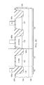
- FIGS. 2A-2D shows cross sectional depictions of a process progression for an example method for forming a BiCMOS IC including a single mask level having both a polysilicon resistor implant and a thru-gate implant, according to an example embodiment.
- the depiction shown in FIG. 2A corresponds to method 100 after step 103 (forming a first mask pattern material 112 ).
- First mask pattern material 112 blocks areas including a portion of the second pwell 132 corresponding the channel region of a later formed NMOS device and later formed contacts to the nwell 135 .
- First mask pattern material 112 is shown with openings over a resistor area 141 where polysilicon resistors are formed, over a BSD class device area 121 where BSD class devices are formed, and over a CMOS device area 131 where NMOS transistors and PMOS transistors (MOS transistors), as well as polysilicon capacitors (poly capacitors) are formed.
- the field dielectric is shown as shallow trench isolation (STI) 110 ′ formed into a semiconductor surface layer 109 on a substrate 108 .
- STI 110 ′ generally surrounds each device.
- a polysilicon layer 120 is shown on a dielectric layer 127 that is on the semiconductor surface layer 109 .
- I 1 has a projected range R P1 that is ⁇ a thickness of the polysilicon layer 120 which implants the polysilicon layer 120 (shown P + doped) except where the first mask pattern material 112 is present.
- I 2 is shown as a thru-gate boron implant which provides the p-dopant for a pbase 122 of an NPN bipolar transistor within the nwell 135 in the BSD device area 121 and p-dopant for a second pwell 132 and a third pwell 137 within the nwell 135 in the CMOS device area 131 .
- the I 2 implant to form the second pwell 132 and third pwell 137 is shown with a mask pattern comprising the first mask pattern material 112 covering the polysilicon gate area and lateral to the resistor area 141 as shown to enable a nwell contact, where I 2 is shown as a tilted implant which can be from 2 degrees to 45 degrees for forming the second pwell 132 .
- both I 1 and I 2 comprise boron implantation.
- I 2 can be a thru-gate n-type (e.g., phosphorus) implant to create an n-base for a PNP bipolar, or a second nwell within a p-region (e.g., pwell) in the CMOS device area 131 .
- n-type e.g., phosphorus
- FIG. 2B shows the first mask pattern material 112 removed and a polysilicon mask pattern material 113 formed on portions of the polysilicon layer 120 .
- FIG. 2C shows the polysilicon layer 120 after etching to provide at least a polysilicon resistor 120 a (corresponding to step 106 ) in the resistor area 141 and a polysilicon electrode 120 c for the poly capacitor in the CMOS device area 131 .
- the polysilicon that will later be the gate electrode 120 b for an NMOS device in the CMOS device area 131 is also shown formed.
- FIG. 2D shows arrows representing an n+ SD implant (after a P+ implant to form a p+ base contact (base contact) 124 for the NPN bipolar transistor (shown as P+SD) in the BSD device area 121 and a p+ pwell contact (not shown) for the NMOS transistor in the CMOS device area 131 ) to provide the n+ emitter 123 for an NPN bipolar transistor in the BSD device area 121 and an n+ SD implant for forming n+ SDs 133 for an NMOS transistor in the CMOS device area 131 .
- the polysilicon resistor 120 a in the resistor area 141 and the area around the poly capacitor comprising polysilicon electrode 120 c , and base contact 124 is masked by the masking material 114 .
- the body of poly resistor 120 a is covered by a silicide block (SIBLK) layer 139 (e.g. silicon nitride) which prevents silicide formation and enables obtaining high value sheet resistance ( ⁇ 100 to 5,000 ohms/sq).
- SIBLK silicide block
- the head portion of the poly resistor 120 a (not shown in the figure) is typically not covered by the SIBLK layer 139 to enable low resistance contacts to be formed.
- the SIBLK layer 139 also electrically separates the n+ emitter 123 and base contact 124 of the NPN bipolar transistor shown in FIG. 2 .D.
- the SIBLK layer 139 can be formed prior to the n+ and p+ SD implants and act as an implant mask for the NPN transistor. In another embodiment the SIBLK layer 139 can be formed after the source-drain implants. The SIBLK layer 139 typically remains on the final IC but can also be removed after silicide formation.
- a PMOS transistor 141 is also shown as a block in CMOS device area 131 ′. The gate electrodes of PMOS transistor 141 and poly capacitor 120 a can be made from the same p+ doped polysilicon layer as polysilicon resistor 120 a.
- FIGS. 3A-3D shows cross sectional depictions of a process progression for an example method for forming a BiCMOS IC including a single mask level having both a polysilicon resistor implant and a thru-gate ion implant, according to an another example embodiment.
- FIG. 3A follows FIG. 2A except the thru-gate implant (I 2 ) provides a junction depth that is below the depth of the STI 110 ′.
- FIG. 3B follows FIG. 2B
- FIG. 3C follows FIG. 2C .
- FIG. 3D follows FIG. 2D except there is another p-well contact 136 shown provided for the NMOS transistor in the 3 rd pwell 137 of the CMOS device area 131 .
- the p-base 122 ′ for the NPN transistor in FIG. 3D is wider as compared the p-base 122 for the NPN transistor shown in FIG. 2D
- the NPN transistor in FIG. 3D is a lower gain NPN transistor.
- I 2 can be a thru-gate n-type (e.g., phosphorus) implant to create an n-base for a PNP bipolar transistor, or a second nwell within a p-region (e.g., pwell) in the CMOS device area 131 .
- n-type e.g., phosphorus
- p-region e.g., pwell
- FIGS. 4A-4D shows cross sectional depictions of a process progression for an example method for forming a BiCMOS IC including a single mask level having both a polysilicon resistor implant and a thru-gate implant, according to an yet another example.
- the thru-gate implant is for forming both low Vt and/high Vt MOS transistor using an angled n-type (e.g., phosphorous) or boron implant.
- a BSD class device area 121 is also present for this process embodiment as with other embodiments, such as where bipolar transistors are formed, it is not shown in FIGS. 4A-4D .
- FIG. 4A follows FIG. 2A except the semiconductor surface layer 109 is shown being p-type and I 2 (the thru-gate implant) can be an n-type implant to form an nwell or a p-type implant to form a pwell shown as nwell/pwell 432 .
- FIG. 4B follows FIG. 2B except now the polysilicon mask pattern material 113 is on the polysilicon layer 120 over two different CMOS device areas shown as CMOS device area 131 a and the CMOS device area 131 b .
- FIG. 4C follows FIG. 2C except the gates are now shown as gate 120 b 1 over CMOS device area 131 a and gate 120 b 2 over the CMOS device area 131 b.
- FIG. 4D follows FIG. 2D except the MOS devices are both shown as PMOS devices and p+ SD regions 461 formed in both CMOS device area 131 a and CMOS device area 131 b .
- the PMOS device having gate 120 b 1 in CMOS device area 131 a receives a PSD implant to form PSD regions 461
- the MOS device having gate 120 b 2 in CMOS device area 131 b receives the PSD implant to form PSD regions 461
- the MOS device having gate 120 b 2 in CMOS device area 131 b receives the PSD implant to form PSD regions 461 , as well as a PLDD implant to form PLDD region 462 and an angled pocket implant to form pocket region 463 .
- the CMOS device area 131 a is masked to prevent the PLDD and pocket implants.
- PLDD implant to form PLDD region 462 and angled pocket implant to form pocket region 463 in CMOS device area 131 b results in a Vt difference between the PMOS devices in CMOS device area 131 a and the PMOS devices in CMOS device area 131 b , such as a difference in Vt of at least (>) 50 mV.
- FIGS. 5A-5B show a variant of the process flow shown in FIGS. 4A-4D for forming both replacement metal gate low Vt and high Vt PMOS transistors.
- FIG. 5A tracks FIG. 4D described above.
- the nwell is shown as 532 .
- FIG. 5B shows removal of the gate 120 b 1 over CMOS device area 131 a and the gate 120 b 2 over CMOS device area 131 b (while protecting polysilicon resistor 120 a ), and replacement gates with replacement gate PMOS gate material 520 .
- FIGS. 6A-6B show a variant of the process flow shown in FIGS. 4A-4D for forming both replacement metal gate low Vt and high Vt NMOS transistors.
- FIG. 6A tracks FIG. 4D described above except reverse the doping type in the semiconductor surface layer 109 .
- the pwell is shown as 632 .
- NSD regions 661 , NLDD regions 662 and pocket regions 663 are shown.
- FIG. 6B shows removal of the gate 120 b 1 over CMOS device area 131 a and gate 120 b 2 over CMOS device area 131 b (while protecting polysilicon resistor 120 a ), and replacement gates with a replacement gate NMOS gate material 570 .
- a disclosed NPN bipolar transistor having a SIBLK material can add an additional PSD (P+) contact to the nwell 135 .
- a Schottky diode can be formed comprising a silicide contact on a lightly doped I 2 implanted region which does not receive either an NSD (n+) or PSD (p+) implant.
- a p-channel JFET can be formed from adding an n-type gate into the pbase 122 of the in-process device shown in the BSD device area 121 .
- the isolation dielectric in the resistor area 141 under the polysilicon resistor 120 a has a dopant gradient and a significant surface dopant concentration.
- the top 0.1 ⁇ m portion of the isolation dielectric (such as STI 110 ′) has a peak boron or n-type dopant concentration of at least 1 ⁇ 10 17 cm ⁇ 3 and a bottom 0.1 ⁇ m portion of the isolation dielectric has a peak boron or n-type dopant concentration of less than ( ⁇ ) 1 ⁇ 10 14 cm ⁇ 3 .
- Disclosed embodiments can be used to form semiconductor die that may be integrated into a variety of assembly flows to form a variety of different devices and related products.
- the semiconductor die may include various elements therein and/or layers thereon, including barrier layers, dielectric layers, device structures, active elements and passive elements including source regions, drain regions, bit lines, bases, emitters, collectors, conductive lines, conductive vias, etc.
- the semiconductor die can be formed from a variety of processes including bipolar, Insulated Gate Bipolar Transistor (IGBT), CMOS, BiCMOS and MEMS.
- IGBT Insulated Gate Bipolar Transistor
Abstract
A method of forming an IC includes providing a field dielectric in a portion of a semiconductor surface, a bipolar or Schottky diode (BSD) class device area, a CMOS transistor area, and a resistor area. A polysilicon layer is deposited to provide a polysilicon gate area for MOS transistors in the CMOS transistor area, over the BSD class device area, and over the field dielectric for providing a polysilicon resistor in the resistor area. A first mask pattern is formed on the polysilicon layer. Using the first mask pattern, first implanting (I1) of the polysilicon resistor providing a first projected range (RP1)<a thickness of the polysilicon layer and second implanting (I2) providing a second RP (RP2), where RP2>RP1. I2 provides a CMOS implant into the semiconductor surface layer in the CMOS transistor area and/or a BSD implant into the semiconductor surface layer in the BSD area.
Description
Disclosed embodiments relate to BiCMOS semiconductor processing.
BiCMOS technology combines bipolar technology and CMOS technology. CMOS technology offers lower power dissipation, smaller noise margins, and higher packing density. Bipolar technology provides high switching and input/output I/O speed and good noise performance. BiCMOS technology accomplishes improved speed over CMOS and lower power dissipation as compared to bipolar technology.
If existing CMOS implants are used for bipolar devices, then the bipolar gain or some other parameter or feature is generally compromised. Accordingly, a drawback of adding bipolar transistors in a CMOS process flow is extra mask levels and implants needed to provide good performance for both the bipolar devices and CMOS devices. The extra mask levels results in a process cost increase and added defect density as compared to conventional CMOS technology.
This Summary is provided to introduce a brief selection of disclosed concepts in a simplified form that are further described below in the Detailed Description including the drawings provided. This Summary is not intended to limit the claimed subject matter's scope.
Disclosed embodiments include a BiCMOS process flow that includes using a single mask level for ion implanting a polysilicon layer for forming a polysilicon resistor on top of a field dielectric and also a deeper p-type (e.g. boron) or an n-type (e.g., phosphorus) dopant implant that penetrates thru the polysilicon layer (referred to herein as being a “thru-gate implant”) into the semiconductor surface layer thereunder. The thru-gate implant can provide a second pwell/nwell and/or a deep nwell for CMOS devices. The thru-gate implant can also be used to form a bipolar or Schottky diode (BSD) device, including the base of a vertical NPN or vertical PNP bipolar transistor. As the polysilicon resistor is generally on top of field oxide, the thru-gate implant despite penetrating thru the polysilicon layer into the underlying field oxide is a harmless fingerprint for disclosed methods.
Disclosed embodiments contain a method of forming an integrated circuit (IC) including providing a field dielectric in a portion of a semiconductor surface layer, a bipolar or Schottky diode (BSD) class device area, a CMOS transistor area, and a resistor area. A polysilicon layer is deposited over a CMOS transistor area for providing polysilicon gates for MOS transistors and capacitors in the CMOS transistor area, over the BSD class device area, and over the field dielectric for providing a polysilicon resistor in the resistor area. A first mask pattern is formed on the polysilicon layer. Using the first mask pattern, first implanting (I1) the polysilicon resistor providing a first projected range (RP1)<a thickness of the polysilicon layer and second implanting (I2) providing a second RP (RP2), where RP2>RP1. I2 provides a CMOS implant into the semiconductor surface layer in the CMOS transistor area and/or a BSD implant into the semiconductor surface layer in the BSD area.
Reference will now be made to the accompanying drawings, which are not necessarily drawn to scale, wherein:
Example embodiments are described with reference to the drawings, wherein like reference numerals are used to designate similar or equivalent elements. Illustrated ordering of acts or events should not be considered as limiting, as some acts or events may occur in different order and/or concurrently with other acts or events. Furthermore, some illustrated acts or events may not be required to implement a methodology in accordance with this disclosure.
The field dielectric can comprise a LOCal Oxidation of Silicon (LOCOS) oxide or a trench isolation structure such as shallow trench isolation (STI) or deep trench isolation (DTI). A thickness of the field dielectric can be from 0.1 μm to 3 μm.
Two implants are shown in FIG. 2A , I1 (step 104) and I2 (step 105). As noted above I1 has a projected range RP1 that is <a thickness of the polysilicon layer 120 which implants the polysilicon layer 120 (shown P+ doped) except where the first mask pattern material 112 is present. I2 is shown as a thru-gate boron implant which provides the p-dopant for a pbase 122 of an NPN bipolar transistor within the nwell 135 in the BSD device area 121 and p-dopant for a second pwell 132 and a third pwell 137 within the nwell 135 in the CMOS device area 131. The I2 implant to form the second pwell 132 and third pwell 137 is shown with a mask pattern comprising the first mask pattern material 112 covering the polysilicon gate area and lateral to the resistor area 141 as shown to enable a nwell contact, where I2 is shown as a tilted implant which can be from 2 degrees to 45 degrees for forming the second pwell 132.
The p-type/nwell junction is shown above the bottom of the field dielectric shown as STI 110′. Thus, as shown in FIG. 2A , both I1 and I2 comprise boron implantation. However, I2 can be a thru-gate n-type (e.g., phosphorus) implant to create an n-base for a PNP bipolar, or a second nwell within a p-region (e.g., pwell) in the CMOS device area 131. One can also perform both boron and phosphorous thru-gate implants in the same regions to form vertical diffusion resistors.
In the example shown in FIG. 2D , the body of poly resistor 120 a is covered by a silicide block (SIBLK) layer 139 (e.g. silicon nitride) which prevents silicide formation and enables obtaining high value sheet resistance (˜100 to 5,000 ohms/sq). The head portion of the poly resistor 120 a (not shown in the figure) is typically not covered by the SIBLK layer 139 to enable low resistance contacts to be formed. The SIBLK layer 139 also electrically separates the n+ emitter 123 and base contact 124 of the NPN bipolar transistor shown in FIG. 2 .D. In one embodiment, the SIBLK layer 139 can be formed prior to the n+ and p+ SD implants and act as an implant mask for the NPN transistor. In another embodiment the SIBLK layer 139 can be formed after the source-drain implants. The SIBLK layer 139 typically remains on the final IC but can also be removed after silicide formation. A PMOS transistor 141 is also shown as a block in CMOS device area 131′. The gate electrodes of PMOS transistor 141 and poly capacitor 120 a can be made from the same p+ doped polysilicon layer as polysilicon resistor 120 a.
Regarding forming devices other than bipolars in the BSD device area 121, for example, to form an SCR a disclosed NPN bipolar transistor having a SIBLK material (such as shown in FIG. 2D as 139) can add an additional PSD (P+) contact to the nwell 135. A Schottky diode can be formed comprising a silicide contact on a lightly doped I2 implanted region which does not receive either an NSD (n+) or PSD (p+) implant. A p-channel JFET can be formed from adding an n-type gate into the pbase 122 of the in-process device shown in the BSD device area 121.
One distinctive feature believed to be unique for ICs fabricated using disclosed methods including a single mask level having both a polysilicon resistor implant and a thru-gate ion implant, is that due to the thru-gate implant the isolation dielectric in the resistor area 141 under the polysilicon resistor 120 a has a dopant gradient and a significant surface dopant concentration. Specifically, the top 0.1 μm portion of the isolation dielectric (such as STI 110′) has a peak boron or n-type dopant concentration of at least 1×1017 cm−3 and a bottom 0.1 μm portion of the isolation dielectric has a peak boron or n-type dopant concentration of less than (<) 1×1014 cm−3.
Disclosed embodiments can be used to form semiconductor die that may be integrated into a variety of assembly flows to form a variety of different devices and related products. The semiconductor die may include various elements therein and/or layers thereon, including barrier layers, dielectric layers, device structures, active elements and passive elements including source regions, drain regions, bit lines, bases, emitters, collectors, conductive lines, conductive vias, etc. Moreover, the semiconductor die can be formed from a variety of processes including bipolar, Insulated Gate Bipolar Transistor (IGBT), CMOS, BiCMOS and MEMS.
Those skilled in the art to which this disclosure relates will appreciate that many other embodiments and variations of embodiments are possible within the scope of the claimed invention, and further additions, deletions, substitutions and modifications may be made to the described embodiments without departing from the scope of this disclosure.
Claims (12)
1. A method of forming an integrated circuit (IC), comprising:
providing a substrate having a semiconductor surface layer thereon including a field dielectric in a portion of said semiconductor surface layer including a bipolar or Schottky diode (BSD) class device area, a CMOS transistor area, and a resistor area;
depositing a polysilicon layer over said CMOS transistor area to provide a polysilicon gate area for MOS transistors in said CMOS transistor area, over said BSD class device area, and over said field dielectric for providing a polysilicon resistor in said resistor area;
forming a first mask pattern on said polysilicon layer;
using said first mask pattern, first implanting (I1) said polysilicon resistor with a first dopant at a first implant energy providing a first projected range (RP1) for said first dopant that is less than (<) a thickness of said polysilicon layer;
using said first mask pattern, second implanting (I2) with a second dopant at a second implant energy providing a second RP (RP2), wherein said RP2>said RP1, said I2 providing at least one of a CMOS implant into said semiconductor surface layer in said CMOS transistor area and a BSD implant into said semiconductor surface layer in said BSD class device area.
2. The method of claim 1 , wherein said first mask pattern covers said polysilicon gate area and exposes at least a portion of said CMOS transistor area, and wherein said CMOS implant comprises an implant for forming a well for said MOS transistors in said semiconductor surface layer including under said polysilicon gate area, and wherein said first mask pattern exposes at least a portion of said BSD class device area, and wherein said BSD implant comprises forming a doped region for at least one device type in said BSD class device area.
3. The method of claim 2 , wherein said doped region is a pbase region, and further comprising after said I1 and said I2:
patterning said polysilicon layer to provide said polysilicon resistor and said polysilicon gate area for said MOS transistors;
masking said polysilicon resistor and a portion of said pbase region, and
first n-type implanting within said pbase region to form a n+ emitter for a vertical bipolar device, first boron implanting said pbase region to form a p+ base contact, and second n-type implanting to form ntype lightly doped drains (NLDDs) and third n-type implanting to form n+ source/drains (SDs) in said well.
4. The method of claim 3 , wherein said I2 comprises using boron to form said pbase region for a vertical bipolar device in said BSD class device area and a pwell for an NMOS device in said CMOS transistor area, further comprising after said I1 and said I2:
patterning said polysilicon layer to provide said polysilicon resistor and said polysilicon gate area for said NMOS device, and
masking said polysilicon resistor while implanting within said pbase region and for said vertical bipolar devices to form an n+ emitter, and implanting at least NLDDs and n+ source/drains in said pwell.
5. The method of claim 1 , wherein said I2 comprises said using boron to form a pwell for NMOS devices in said CMOS transistor area, further comprising after said I1 and said I2:
patterning said polysilicon layer to provide said polysilicon resistor and said polysilicon gate area for said NMOS devices, and
implanting at least NLDDs and n+ source/drains in said pwell.
6. The method of claim 5 , further comprising:
removing said polysilicon gate area for at least a first of said NMOS devices, and
forming a replacement metal gates for said first NMOS device.
7. The method of claim 1 , wherein said I2 comprises said using an n-type dopant to form an nwell for PMOS devices in said CMOS transistor area, further comprising after said I1 and said I2:
patterning said polysilicon layer to provide said polysilicon resistor and said polysilicon gate area for said PMOS devices, and
implanting at least PLDDs and p+ source/drains in said nwell.
8. The method of claim 7 , further comprising:
removing said polysilicon gate area for at least a first of said PMOS devices, and
forming a replacement metal gate for said first PMOS device.
9. The method of claim 1 , wherein said field dielectric comprises trench isolation and wherein said polysilicon resistor is on top of said trench isolation.
10. The method of claim 9 , wherein said field dielectric in said resistor area under said polysilicon resistor has a dopant gradient, said dopant gradient comprising a top 0.1 μm portion of said field dielectric having at least one of a peak boron and n-type dopant concentration of at least 1×1017 cm−3 and a bottom 0.1 μm portion of said field dielectric having at least one of a peak boron and n-type dopant concentration of less than (<) 1×1014 cm−3.
11. The method of claim 1 , wherein said thickness of said polysilicon layer is 50 nm to 200 nm, wherein said I1 comprises a boron dose of >1×1015 cm−2, and said polysilicon resistor is a Zero Temperature Coefficient Resistor (ZTCR) having a TCR at 25° C. of from −100 ppm to +100 ppm.
12. The method of claim 1 , wherein said polysilicon layer also provides polysilicon capacitors in said CMOS transistor area.
Priority Applications (2)
| Application Number | Priority Date | Filing Date | Title |
|---|---|---|---|
| US15/060,261 US9761581B1 (en) | 2016-03-03 | 2016-03-03 | Single mask level including a resistor and a through-gate implant |
| US15/669,246 US10026730B2 (en) | 2016-03-03 | 2017-08-04 | Single mask level including a resistor and a through-gate implant |
Applications Claiming Priority (1)
| Application Number | Priority Date | Filing Date | Title |
|---|---|---|---|
| US15/060,261 US9761581B1 (en) | 2016-03-03 | 2016-03-03 | Single mask level including a resistor and a through-gate implant |
Related Child Applications (1)
| Application Number | Title | Priority Date | Filing Date |
|---|---|---|---|
| US15/669,246 Division US10026730B2 (en) | 2016-03-03 | 2017-08-04 | Single mask level including a resistor and a through-gate implant |
Publications (2)
| Publication Number | Publication Date |
|---|---|
| US20170256535A1 US20170256535A1 (en) | 2017-09-07 |
| US9761581B1 true US9761581B1 (en) | 2017-09-12 |
Family
ID=59723721
Family Applications (2)
| Application Number | Title | Priority Date | Filing Date |
|---|---|---|---|
| US15/060,261 Active US9761581B1 (en) | 2016-03-03 | 2016-03-03 | Single mask level including a resistor and a through-gate implant |
| US15/669,246 Active US10026730B2 (en) | 2016-03-03 | 2017-08-04 | Single mask level including a resistor and a through-gate implant |
Family Applications After (1)
| Application Number | Title | Priority Date | Filing Date |
|---|---|---|---|
| US15/669,246 Active US10026730B2 (en) | 2016-03-03 | 2017-08-04 | Single mask level including a resistor and a through-gate implant |
Country Status (1)
| Country | Link |
|---|---|
| US (2) | US9761581B1 (en) |
Families Citing this family (4)
| Publication number | Priority date | Publication date | Assignee | Title |
|---|---|---|---|---|
| DE102017205448A1 (en) * | 2017-03-30 | 2018-10-04 | Infineon Technologies Ag | A high frequency resistance element |
| US10340357B2 (en) * | 2017-09-25 | 2019-07-02 | Taiwan Semiconductor Manufacturing Co., Ltd. | Dishing prevention dummy structures for semiconductor devices |
| US11335674B2 (en) | 2019-06-27 | 2022-05-17 | Globalfoundries U.S. Inc. | Diode triggered silicon controlled rectifier (SCR) with hybrid diodes |
| US11430881B2 (en) * | 2020-03-05 | 2022-08-30 | Globalfoundries U.S. Inc. | Diode triggered compact silicon controlled rectifier |
Citations (8)
| Publication number | Priority date | Publication date | Assignee | Title |
|---|---|---|---|---|
| US4902640A (en) * | 1987-04-17 | 1990-02-20 | Tektronix, Inc. | High speed double polycide bipolar/CMOS integrated circuit process |
| US5139966A (en) * | 1990-04-02 | 1992-08-18 | National Semiconductor Corporation | Low resistance silicided substrate contact |
| US5414291A (en) * | 1993-01-30 | 1995-05-09 | Sony Corporation | Semiconductor device and process for fabricating the same |
| US6351021B1 (en) * | 1999-07-01 | 2002-02-26 | Intersil Americas Inc. | Low temperature coefficient resistor (TCRL) |
| US20030157778A1 (en) * | 1999-07-01 | 2003-08-21 | Intersil Corporation | BiCMOS process with low temperature coefficient resistor (TCRL) |
| US20070246780A1 (en) * | 2006-04-20 | 2007-10-25 | Renesas Technology Corp. | Semiconductor device and a method of manufacturing the same |
| US20100178740A1 (en) * | 2007-10-18 | 2010-07-15 | Texas Instruments Incorporated | Bipolar transistors with resistors |
| US20140167182A1 (en) | 2012-12-17 | 2014-06-19 | Texas Instruments Incorporated | Ztcr poly resistor in replacement gate flow |
-
2016
- 2016-03-03 US US15/060,261 patent/US9761581B1/en active Active
-
2017
- 2017-08-04 US US15/669,246 patent/US10026730B2/en active Active
Patent Citations (8)
| Publication number | Priority date | Publication date | Assignee | Title |
|---|---|---|---|---|
| US4902640A (en) * | 1987-04-17 | 1990-02-20 | Tektronix, Inc. | High speed double polycide bipolar/CMOS integrated circuit process |
| US5139966A (en) * | 1990-04-02 | 1992-08-18 | National Semiconductor Corporation | Low resistance silicided substrate contact |
| US5414291A (en) * | 1993-01-30 | 1995-05-09 | Sony Corporation | Semiconductor device and process for fabricating the same |
| US6351021B1 (en) * | 1999-07-01 | 2002-02-26 | Intersil Americas Inc. | Low temperature coefficient resistor (TCRL) |
| US20030157778A1 (en) * | 1999-07-01 | 2003-08-21 | Intersil Corporation | BiCMOS process with low temperature coefficient resistor (TCRL) |
| US20070246780A1 (en) * | 2006-04-20 | 2007-10-25 | Renesas Technology Corp. | Semiconductor device and a method of manufacturing the same |
| US20100178740A1 (en) * | 2007-10-18 | 2010-07-15 | Texas Instruments Incorporated | Bipolar transistors with resistors |
| US20140167182A1 (en) | 2012-12-17 | 2014-06-19 | Texas Instruments Incorporated | Ztcr poly resistor in replacement gate flow |
Also Published As
| Publication number | Publication date |
|---|---|
| US10026730B2 (en) | 2018-07-17 |
| US20170338223A1 (en) | 2017-11-23 |
| US20170256535A1 (en) | 2017-09-07 |
Similar Documents
| Publication | Publication Date | Title |
|---|---|---|
| US7095094B2 (en) | Multiple doping level bipolar junctions transistors and method for forming | |
| US10026730B2 (en) | Single mask level including a resistor and a through-gate implant | |
| US20050258453A1 (en) | Single poly-emitter PNP using dwell diffusion in a BiCMOS technology | |
| JPH0315346B2 (en) | ||
| KR101480601B1 (en) | Integrated circuit devices with well regions and methods for forming the same | |
| US9812565B2 (en) | N-channel double diffusion MOS transistor with p-type buried layer underneath n-type drift and drain layers, and semiconductor composite device | |
| US8217426B2 (en) | Bipolar transistors with resistors | |
| US9190501B2 (en) | Semiconductor devices including a lateral bipolar structure with high current gains | |
| US10224402B2 (en) | Method of improving lateral BJT characteristics in BCD technology | |
| KR101576675B1 (en) | Semiconductor device and Method for Manufacturing Thereof | |
| US9397164B2 (en) | Deep collector vertical bipolar transistor with enhanced gain | |
| US7772060B2 (en) | Integrated SiGe NMOS and PMOS transistors | |
| US6011283A (en) | Pillar emitter for BiCMOS devices | |
| JP2006505943A (en) | Semiconductor device channel termination | |
| US20090159984A1 (en) | Semiconductor Device and Method for Manufacturing the Same | |
| JPS6255309B2 (en) | ||
| US20090026578A1 (en) | Vertical NPN Transistor Fabricated in a CMOS Process With Improved Electrical Characteristics | |
| US5451530A (en) | Method for forming integrated circuits having buried doped regions | |
| US5310690A (en) | Method for forming integrated circuits having buried doped regions | |
| JP2001291781A (en) | Method for manufacturing semiconductor device | |
| US9847336B2 (en) | Method of forming a junction field effect transistor | |
| KR20090068084A (en) | Semiconductor device and method for manufacturing thereof | |
| KR100971212B1 (en) | semiconductor device and Method for fabricating of the same | |
| KR100247704B1 (en) | Method of fabricating semiconductor device | |
| EP0366967B1 (en) | A method of forming integrated circuits having buried doped regions |
Legal Events
| Date | Code | Title | Description |
|---|---|---|---|
| AS | Assignment |
Owner name: TEXAS INSTRUMENTS INCORPORATED, TEXAS Free format text: ASSIGNMENT OF ASSIGNORS INTEREST;ASSIGNORS:NANDAKUMAR, MAHALINGAM;GRIDER, DOUGLAS TAD, III;REEL/FRAME:037890/0252 Effective date: 20160129 |
|
| STCF | Information on status: patent grant |
Free format text: PATENTED CASE |
|
| MAFP | Maintenance fee payment |
Free format text: PAYMENT OF MAINTENANCE FEE, 4TH YEAR, LARGE ENTITY (ORIGINAL EVENT CODE: M1551); ENTITY STATUS OF PATENT OWNER: LARGE ENTITY Year of fee payment: 4 |