US9761521B1 - Flexible and robust power grid connectivity - Google Patents
Flexible and robust power grid connectivity Download PDFInfo
- Publication number
- US9761521B1 US9761521B1 US14/519,271 US201414519271A US9761521B1 US 9761521 B1 US9761521 B1 US 9761521B1 US 201414519271 A US201414519271 A US 201414519271A US 9761521 B1 US9761521 B1 US 9761521B1
- Authority
- US
- United States
- Prior art keywords
- conductor
- power
- conductors
- polarity
- power grid
- Prior art date
- Legal status (The legal status is an assumption and is not a legal conclusion. Google has not performed a legal analysis and makes no representation as to the accuracy of the status listed.)
- Active, expires
Links
Images


Classifications
-
- H—ELECTRICITY
- H01—ELECTRIC ELEMENTS
- H01L—SEMICONDUCTOR DEVICES NOT COVERED BY CLASS H10
- H01L23/00—Details of semiconductor or other solid state devices
- H01L23/48—Arrangements for conducting electric current to or from the solid state body in operation, e.g. leads, terminal arrangements ; Selection of materials therefor
- H01L23/50—Arrangements for conducting electric current to or from the solid state body in operation, e.g. leads, terminal arrangements ; Selection of materials therefor for integrated circuit devices, e.g. power bus, number of leads
-
- H—ELECTRICITY
- H01—ELECTRIC ELEMENTS
- H01L—SEMICONDUCTOR DEVICES NOT COVERED BY CLASS H10
- H01L23/00—Details of semiconductor or other solid state devices
- H01L23/52—Arrangements for conducting electric current within the device in operation from one component to another, i.e. interconnections, e.g. wires, lead frames
- H01L23/522—Arrangements for conducting electric current within the device in operation from one component to another, i.e. interconnections, e.g. wires, lead frames including external interconnections consisting of a multilayer structure of conductive and insulating layers inseparably formed on the semiconductor body
- H01L23/528—Geometry or layout of the interconnection structure
- H01L23/5286—Arrangements of power or ground buses
-
- H—ELECTRICITY
- H01—ELECTRIC ELEMENTS
- H01L—SEMICONDUCTOR DEVICES NOT COVERED BY CLASS H10
- H01L24/00—Arrangements for connecting or disconnecting semiconductor or solid-state bodies; Methods or apparatus related thereto
- H01L24/01—Means for bonding being attached to, or being formed on, the surface to be connected, e.g. chip-to-package, die-attach, "first-level" interconnects; Manufacturing methods related thereto
- H01L24/42—Wire connectors; Manufacturing methods related thereto
- H01L24/44—Structure, shape, material or disposition of the wire connectors prior to the connecting process
- H01L24/46—Structure, shape, material or disposition of the wire connectors prior to the connecting process of a plurality of wire connectors
-
- H—ELECTRICITY
- H01—ELECTRIC ELEMENTS
- H01L—SEMICONDUCTOR DEVICES NOT COVERED BY CLASS H10
- H01L24/00—Arrangements for connecting or disconnecting semiconductor or solid-state bodies; Methods or apparatus related thereto
- H01L24/80—Methods for connecting semiconductor or other solid state bodies using means for bonding being attached to, or being formed on, the surface to be connected
- H01L24/85—Methods for connecting semiconductor or other solid state bodies using means for bonding being attached to, or being formed on, the surface to be connected using a wire connector
Definitions
- modules On integrated circuits and within chips, power is supplied to modules via a power grid. Due to a lack of standardization for power connections on modules, it can be difficult to ensure that every power pin connects to the power grid. As a result, modules may be underpowered and may not perform as designed. The power pin connections can be mitigated somewhat by carefully placing and offsetting the modules as necessary in order to maximize the number of connections that can be made, but this is a time and labor consuming process that still does not guarantee that every single power pin connection can be made.
- a system for providing power grid connectivity to modules on a chip comprises a means for arranging a set of three conductors next to each other, wherein the three conductors are of two polarities.
- the system also comprises a means for providing power to every power pin on the modules on the chip via the set of three conductors.
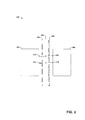
- FIG. 1 is a block diagram illustrating an example, non-limiting embodiment of a power grid interface for providing power to modules in accordance with various aspects described herein.
- Modules 102 and 104 can include power pins 112 , 114 , 116 , and 118 .
- the polarity of power pins 114 and 116 correspond to a first polarity matching the polarity of wires 106 and 110
- the polarity of pins 112 and 118 match the polarity of wire 108 .
- the first polarity of wires 106 and 110 can be Vdd (positive supply) and the polarity of wire 108 can be Vss (negative and/or ground supply).
- Power grid interface 200 includes a set of three wires 206 , 208 , and 210 that are configured to provide electrical power to modules 202 and 204 .
- Module 202 and 204 e.g., intellectual property “IP” cores
- IP intellectual property
- the power pin connectors may not be designed to be compatible at all orientations and alignments in traditional power grid interfaces.
- power connections can be made to each of power pins 212 , 214 , 216 , and 218 .
- modules 502 , 504 , 506 and 508 can be completely surrounded by the power grid interface on all sides, and so depending on the geometry of the chip or module, three or more sides of the modules can have power pins that connect to the power grid interface on the chip.
- an architecture can include an arrangement of electronic hardware (e.g., parallel or serial transistors), processing instructions and a processor, which implement the processing instructions in a manner suitable to the arrangement of electronic hardware.
- an architecture can include a single component (e.g., a transistor, a gate array, . . . ) or an arrangement of components (e.g., a series or parallel arrangement of transistors, a gate array connected with program circuitry, power leads, electrical ground, input signal lines and output signal lines, and so on).
- a system can include one or more components as well as one or more architectures.
- One example system can include a switching block architecture comprising crossed input/output lines and pass gate transistors, as well as power source(s), signal generator(s), communication bus(ses), controllers, I/O interface, address registers, and so on. It is to be appreciated that some overlap in definitions is anticipated, and an architecture or a system can be a stand-alone component, or a component of another architecture, system, etc.
- Computer readable hardware media can include but are not limited to magnetic storage devices (e.g., hard disk, floppy disk, magnetic strips . . . ), optical disks (e.g., compact disk (CD), digital versatile disk (DVD) . . . ), smart cards, and flash memory devices (e.g., card, stick, key drive . . . ).
- Computer-readable transport media can include carrier waves, or the like.
Abstract
Description
Claims (18)
Priority Applications (1)
| Application Number | Priority Date | Filing Date | Title |
|---|---|---|---|
| US14/519,271 US9761521B1 (en) | 2014-10-21 | 2014-10-21 | Flexible and robust power grid connectivity |
Applications Claiming Priority (1)
| Application Number | Priority Date | Filing Date | Title |
|---|---|---|---|
| US14/519,271 US9761521B1 (en) | 2014-10-21 | 2014-10-21 | Flexible and robust power grid connectivity |
Publications (1)
| Publication Number | Publication Date |
|---|---|
| US9761521B1 true US9761521B1 (en) | 2017-09-12 |
Family
ID=59752903
Family Applications (1)
| Application Number | Title | Priority Date | Filing Date |
|---|---|---|---|
| US14/519,271 Active 2034-11-05 US9761521B1 (en) | 2014-10-21 | 2014-10-21 | Flexible and robust power grid connectivity |
Country Status (1)
| Country | Link |
|---|---|
| US (1) | US9761521B1 (en) |
Citations (13)
| Publication number | Priority date | Publication date | Assignee | Title |
|---|---|---|---|---|
| US5945713A (en) | 1994-09-26 | 1999-08-31 | International Business Machines Corporation | Electrostatic discharge protection circuits for mixed voltage interface and multi-rail disconnected power grid applications |
| US6192431B1 (en) * | 1997-12-31 | 2001-02-20 | Intel Corporation | Method and apparatus for configuring the pinout of an integrated circuit |
| US6467074B1 (en) | 2000-03-21 | 2002-10-15 | Ammocore Technology, Inc. | Integrated circuit architecture with standard blocks |
| US20040049754A1 (en) * | 2002-09-06 | 2004-03-11 | Sun Microsystems, Inc. | Method and apparatus for filling and connecting filler material in a layout |
| US6838713B1 (en) * | 1999-07-12 | 2005-01-04 | Virage Logic Corporation | Dual-height cell with variable width power rail architecture |
| US20060095872A1 (en) * | 2002-07-29 | 2006-05-04 | Mcelvain Kenneth S | Integrated circuit devices and methods and apparatuses for designing integrated circuit devices |
| US7462941B2 (en) | 2003-07-30 | 2008-12-09 | Telairity Semiconductor, Inc. | Power grid layout techniques on integrated circuits |
| US20100122230A1 (en) * | 2008-11-13 | 2010-05-13 | Qualcomm Incorporated | Method to Automatically Add Power Line in Channel Between Macros |
| US8086980B2 (en) | 2008-02-15 | 2011-12-27 | International Business Machines Corporation | Efficient power region checking of multi-supply voltage microprocessors |
| US20140013296A1 (en) * | 2012-07-04 | 2014-01-09 | Kabushiki Kaisha Toshiba | Esd analysis apparatus |
| US8738351B2 (en) | 2010-10-12 | 2014-05-27 | International Business Machines Corporation | Historic storage of dual layer power grid connectivity model |
| US8786130B1 (en) | 2013-08-23 | 2014-07-22 | Inoso, Llc | Method of forming an electromechanical power switch for controlling power to integrated circuit devices and related devices |
| US20140264924A1 (en) * | 2010-07-28 | 2014-09-18 | Taiwan Semiconductor Manufacturing Co., Ltd. | Apparatus and method for mitigating dynamic ir voltage drop and electromigration affects |
-
2014
- 2014-10-21 US US14/519,271 patent/US9761521B1/en active Active
Patent Citations (14)
| Publication number | Priority date | Publication date | Assignee | Title |
|---|---|---|---|---|
| US5945713A (en) | 1994-09-26 | 1999-08-31 | International Business Machines Corporation | Electrostatic discharge protection circuits for mixed voltage interface and multi-rail disconnected power grid applications |
| US6192431B1 (en) * | 1997-12-31 | 2001-02-20 | Intel Corporation | Method and apparatus for configuring the pinout of an integrated circuit |
| US6838713B1 (en) * | 1999-07-12 | 2005-01-04 | Virage Logic Corporation | Dual-height cell with variable width power rail architecture |
| US6467074B1 (en) | 2000-03-21 | 2002-10-15 | Ammocore Technology, Inc. | Integrated circuit architecture with standard blocks |
| US8701068B2 (en) | 2002-07-29 | 2014-04-15 | Synopsys, Inc. | Interconnection device in a multi-layer shielding mesh |
| US20060095872A1 (en) * | 2002-07-29 | 2006-05-04 | Mcelvain Kenneth S | Integrated circuit devices and methods and apparatuses for designing integrated circuit devices |
| US20040049754A1 (en) * | 2002-09-06 | 2004-03-11 | Sun Microsystems, Inc. | Method and apparatus for filling and connecting filler material in a layout |
| US7462941B2 (en) | 2003-07-30 | 2008-12-09 | Telairity Semiconductor, Inc. | Power grid layout techniques on integrated circuits |
| US8086980B2 (en) | 2008-02-15 | 2011-12-27 | International Business Machines Corporation | Efficient power region checking of multi-supply voltage microprocessors |
| US20100122230A1 (en) * | 2008-11-13 | 2010-05-13 | Qualcomm Incorporated | Method to Automatically Add Power Line in Channel Between Macros |
| US20140264924A1 (en) * | 2010-07-28 | 2014-09-18 | Taiwan Semiconductor Manufacturing Co., Ltd. | Apparatus and method for mitigating dynamic ir voltage drop and electromigration affects |
| US8738351B2 (en) | 2010-10-12 | 2014-05-27 | International Business Machines Corporation | Historic storage of dual layer power grid connectivity model |
| US20140013296A1 (en) * | 2012-07-04 | 2014-01-09 | Kabushiki Kaisha Toshiba | Esd analysis apparatus |
| US8786130B1 (en) | 2013-08-23 | 2014-07-22 | Inoso, Llc | Method of forming an electromechanical power switch for controlling power to integrated circuit devices and related devices |
Similar Documents
| Publication | Publication Date | Title |
|---|---|---|
| EP3111449B1 (en) | Write operations in spin transfer torque memory | |
| US10224110B2 (en) | Memory card | |
| US10332594B2 (en) | Semiconductor memory device with in memory logic operations | |
| US9552854B1 (en) | Register files including distributed capacitor circuit blocks | |
| US9595966B2 (en) | Level shifter and non-volatile memory device using the same | |
| US20090168483A1 (en) | Ultra low voltage and minimum operating voltage tolerant register file | |
| US9305625B2 (en) | Apparatuses and methods for unit identification in a master/slave memory stack | |
| CN104052432A (en) | Data-retained power-gating circuit and devices including the same | |
| US9831877B2 (en) | Integrated circuit and semiconductor device including the same | |
| US10884956B2 (en) | I/O bus shared memory system | |
| KR20210048393A (en) | 3t2r binary weight cell with high on/off for memory device programmed with transverse currents | |
| KR20200105994A (en) | 4t4r ternary weight cell with high on/off ratio background | |
| US10885945B2 (en) | Apparatus and methods to perform read-while write (RWW) operations | |
| US11386254B2 (en) | Semiconductor circuit and semiconductor circuit layout system | |
| US9761521B1 (en) | Flexible and robust power grid connectivity | |
| US10311923B2 (en) | Input circuit of three-dimensional semiconductor apparatus capable of enabling testing and direct access | |
| CN105608033B (en) | Semiconductor device and method of operating the same | |
| US20170060801A1 (en) | Semiconductor system and controlling method thereof | |
| CN113935278A (en) | Method for designing semiconductor chip and computing device for executing the method | |
| US9575124B2 (en) | Systems and methods for operating high voltage switches | |
| US10566068B2 (en) | Semiconductor storage device and method for controlling semiconductor storage device | |
| US20120324247A1 (en) | Power supply circuit for cpu | |
| CN101841640B (en) | Data stream processing programmable logic chip and set-top box | |
| US20240127896A1 (en) | Deck reset read | |
| US8847651B1 (en) | Apparatus, method and system for implementing a hardware interface pinout |
Legal Events
| Date | Code | Title | Description |
|---|---|---|---|
| AS | Assignment |
Owner name: APPLIED MICRO CIRCUITS CORPORATION, CALIFORNIA Free format text: ASSIGNMENT OF ASSIGNORS INTEREST;ASSIGNORS:JANGITY, ARUN;GBALAKRISHNAN, SRINI;CHONG, TAI;SIGNING DATES FROM 20150107 TO 20150129;REEL/FRAME:034878/0027 |
|
| AS | Assignment |
Owner name: MACOM CONNECTIVITY SOLUTIONS, LLC, MASSACHUSETTS Free format text: MERGER AND CHANGE OF NAME;ASSIGNORS:APPLIED MICRO CIRCUITS CORPORATION;MACOM CONNECTIVITY SOLUTIONS, LLC;MACOM CONNECTIVITY SOLUTIONS, LLC;SIGNING DATES FROM 20170126 TO 20170127;REEL/FRAME:042176/0185 |
|
| AS | Assignment |
Owner name: GOLDMAN SACHS BANK USA, AS COLLATERAL AGENT, NEW YORK Free format text: SECURITY INTEREST;ASSIGNOR:MACOM CONNECTIVITY SOLUTIONS, LLC (SUCCESSOR TO APPLIED MICRO CIRCUITS CORPORATION);REEL/FRAME:042444/0891 Effective date: 20170504 Owner name: GOLDMAN SACHS BANK USA, AS COLLATERAL AGENT, NEW Y Free format text: SECURITY INTEREST;ASSIGNOR:MACOM CONNECTIVITY SOLUTIONS, LLC (SUCCESSOR TO APPLIED MICRO CIRCUITS CORPORATION);REEL/FRAME:042444/0891 Effective date: 20170504 |
|
| STCF | Information on status: patent grant |
Free format text: PATENTED CASE |
|
| AS | Assignment |
Owner name: MACOM CONNECTIVITY SOLUTIONS, LLC (SUCCESSOR TO APPLIED MICRO CIRCUITS CORPORATION), MASSACHUSETTS Free format text: RELEASE BY SECURED PARTY;ASSIGNOR:GOLDMAN SACHS BANK USA, AS COLLATERAL AGENT;REEL/FRAME:044652/0609 Effective date: 20171027 Owner name: MACOM CONNECTIVITY SOLUTIONS, LLC (SUCCESSOR TO AP Free format text: RELEASE BY SECURED PARTY;ASSIGNOR:GOLDMAN SACHS BANK USA, AS COLLATERAL AGENT;REEL/FRAME:044652/0609 Effective date: 20171027 |
|
| AS | Assignment |
Owner name: PROJECT DENVER INTERMEDIATE HOLDINGS LLC, CALIFORNIA Free format text: ASSIGNMENT OF ASSIGNORS INTEREST;ASSIGNOR:MACOM CONNECTIVITY SOLUTIONS, LLC;REEL/FRAME:044798/0599 Effective date: 20171025 Owner name: PROJECT DENVER INTERMEDIATE HOLDINGS LLC, CALIFORN Free format text: ASSIGNMENT OF ASSIGNORS INTEREST;ASSIGNOR:MACOM CONNECTIVITY SOLUTIONS, LLC;REEL/FRAME:044798/0599 Effective date: 20171025 |
|
| AS | Assignment |
Owner name: AMPERE COMPUTING LLC, CALIFORNIA Free format text: CHANGE OF NAME;ASSIGNOR:PROJECT DENVER INTERMEDIATE HOLDINGS LLC;REEL/FRAME:044717/0683 Effective date: 20171129 |
|
| FEPP | Fee payment procedure |
Free format text: ENTITY STATUS SET TO SMALL (ORIGINAL EVENT CODE: SMAL) |
|
| FEPP | Fee payment procedure |
Free format text: ENTITY STATUS SET TO UNDISCOUNTED (ORIGINAL EVENT CODE: BIG.); ENTITY STATUS OF PATENT OWNER: LARGE ENTITY |
|
| MAFP | Maintenance fee payment |
Free format text: PAYMENT OF MAINTENANCE FEE, 4TH YEAR, LARGE ENTITY (ORIGINAL EVENT CODE: M1551); ENTITY STATUS OF PATENT OWNER: LARGE ENTITY Year of fee payment: 4 |