US9753001B1 - Polymer nanofiber based reversible nano-switch/sensor diode (nanoSSSD) device - Google Patents
Polymer nanofiber based reversible nano-switch/sensor diode (nanoSSSD) device Download PDFInfo
- Publication number
- US9753001B1 US9753001B1 US14/672,673 US201514672673A US9753001B1 US 9753001 B1 US9753001 B1 US 9753001B1 US 201514672673 A US201514672673 A US 201514672673A US 9753001 B1 US9753001 B1 US 9753001B1
- Authority
- US
- United States
- Prior art keywords
- switching
- nano
- sensing device
- nanostructure
- polymer nanofiber
- Prior art date
- Legal status (The legal status is an assumption and is not a legal conclusion. Google has not performed a legal analysis and makes no representation as to the accuracy of the status listed.)
- Active, expires
Links
- 239000002121 nanofiber Substances 0.000 title claims abstract description 23
- 229920000642 polymer Polymers 0.000 title claims abstract description 21
- 230000002441 reversible effect Effects 0.000 title claims description 7
- 239000002086 nanomaterial Substances 0.000 claims abstract description 59
- 239000000758 substrate Substances 0.000 claims abstract description 45
- 230000009977 dual effect Effects 0.000 claims abstract description 27
- 230000006870 function Effects 0.000 claims abstract description 25
- XUIMIQQOPSSXEZ-UHFFFAOYSA-N Silicon Chemical compound [Si] XUIMIQQOPSSXEZ-UHFFFAOYSA-N 0.000 claims description 22
- 229910052710 silicon Inorganic materials 0.000 claims description 22
- 239000010703 silicon Substances 0.000 claims description 22
- 230000005855 radiation Effects 0.000 claims description 17
- VYPSYNLAJGMNEJ-UHFFFAOYSA-N Silicium dioxide Chemical group O=[Si]=O VYPSYNLAJGMNEJ-UHFFFAOYSA-N 0.000 claims description 12
- 239000002019 doping agent Substances 0.000 claims description 8
- 239000000377 silicon dioxide Substances 0.000 claims description 6
- 235000012239 silicon dioxide Nutrition 0.000 claims description 3
- OKTJSMMVPCPJKN-UHFFFAOYSA-N Carbon Chemical compound [C] OKTJSMMVPCPJKN-UHFFFAOYSA-N 0.000 description 55
- 229910021389 graphene Inorganic materials 0.000 description 41
- 241000894007 species Species 0.000 description 24
- QGZKDVFQNNGYKY-UHFFFAOYSA-N Ammonia Chemical compound N QGZKDVFQNNGYKY-UHFFFAOYSA-N 0.000 description 21
- 229910000069 nitrogen hydride Inorganic materials 0.000 description 14
- 239000010410 layer Substances 0.000 description 12
- 238000000034 method Methods 0.000 description 12
- MWUXSHHQAYIFBG-UHFFFAOYSA-N nitrogen oxide Inorganic materials O=[N] MWUXSHHQAYIFBG-UHFFFAOYSA-N 0.000 description 8
- 239000007789 gas Substances 0.000 description 7
- 238000004519 manufacturing process Methods 0.000 description 7
- 230000004044 response Effects 0.000 description 7
- 238000013459 approach Methods 0.000 description 6
- 238000001179 sorption measurement Methods 0.000 description 6
- CURLTUGMZLYLDI-UHFFFAOYSA-N Carbon dioxide Chemical compound O=C=O CURLTUGMZLYLDI-UHFFFAOYSA-N 0.000 description 5
- 229910002804 graphite Inorganic materials 0.000 description 5
- 239000010439 graphite Substances 0.000 description 5
- 238000012544 monitoring process Methods 0.000 description 5
- 239000002341 toxic gas Substances 0.000 description 5
- 238000003795 desorption Methods 0.000 description 4
- 238000001514 detection method Methods 0.000 description 4
- 239000012212 insulator Substances 0.000 description 4
- UGFAIRIUMAVXCW-UHFFFAOYSA-N Carbon monoxide Chemical compound [O+]#[C-] UGFAIRIUMAVXCW-UHFFFAOYSA-N 0.000 description 3
- 229910021529 ammonia Inorganic materials 0.000 description 3
- 230000008901 benefit Effects 0.000 description 3
- 229910002092 carbon dioxide Inorganic materials 0.000 description 3
- 229910002091 carbon monoxide Inorganic materials 0.000 description 3
- 239000002322 conducting polymer Substances 0.000 description 3
- 229920001940 conductive polymer Polymers 0.000 description 3
- 238000005516 engineering process Methods 0.000 description 3
- 239000000463 material Substances 0.000 description 3
- 230000035945 sensitivity Effects 0.000 description 3
- 239000002356 single layer Substances 0.000 description 3
- 125000004429 atom Chemical group 0.000 description 2
- 239000001569 carbon dioxide Substances 0.000 description 2
- 230000002708 enhancing effect Effects 0.000 description 2
- 239000002360 explosive Substances 0.000 description 2
- 239000010931 gold Substances 0.000 description 2
- 230000036541 health Effects 0.000 description 2
- 229930195733 hydrocarbon Natural products 0.000 description 2
- 150000002430 hydrocarbons Chemical class 0.000 description 2
- 239000001257 hydrogen Substances 0.000 description 2
- 229910052739 hydrogen Inorganic materials 0.000 description 2
- 125000004435 hydrogen atom Chemical class [H]* 0.000 description 2
- 229910044991 metal oxide Inorganic materials 0.000 description 2
- 150000004706 metal oxides Chemical class 0.000 description 2
- 238000001000 micrograph Methods 0.000 description 2
- 230000004048 modification Effects 0.000 description 2
- 238000012986 modification Methods 0.000 description 2
- 230000003287 optical effect Effects 0.000 description 2
- 230000008569 process Effects 0.000 description 2
- 239000004065 semiconductor Substances 0.000 description 2
- 239000000126 substance Substances 0.000 description 2
- 231100000331 toxic Toxicity 0.000 description 2
- 230000002588 toxic effect Effects 0.000 description 2
- RMBFBMJGBANMMK-UHFFFAOYSA-N 2,4-dinitrotoluene Chemical compound CC1=CC=C([N+]([O-])=O)C=C1[N+]([O-])=O RMBFBMJGBANMMK-UHFFFAOYSA-N 0.000 description 1
- IJGRMHOSHXDMSA-UHFFFAOYSA-N Atomic nitrogen Chemical compound N#N IJGRMHOSHXDMSA-UHFFFAOYSA-N 0.000 description 1
- RYGMFSIKBFXOCR-UHFFFAOYSA-N Copper Chemical compound [Cu] RYGMFSIKBFXOCR-UHFFFAOYSA-N 0.000 description 1
- 241000282412 Homo Species 0.000 description 1
- -1 NO and NO2) Chemical compound 0.000 description 1
- 229910000831 Steel Inorganic materials 0.000 description 1
- 230000004075 alteration Effects 0.000 description 1
- 230000003466 anti-cipated effect Effects 0.000 description 1
- 230000009118 appropriate response Effects 0.000 description 1
- 229910052799 carbon Inorganic materials 0.000 description 1
- 230000015556 catabolic process Effects 0.000 description 1
- 238000005229 chemical vapour deposition Methods 0.000 description 1
- 239000003086 colorant Substances 0.000 description 1
- 238000010276 construction Methods 0.000 description 1
- 229910052802 copper Inorganic materials 0.000 description 1
- 239000010949 copper Substances 0.000 description 1
- 239000013078 crystal Substances 0.000 description 1
- 238000006731 degradation reaction Methods 0.000 description 1
- 230000007613 environmental effect Effects 0.000 description 1
- 238000004299 exfoliation Methods 0.000 description 1
- PCHJSUWPFVWCPO-UHFFFAOYSA-N gold Chemical compound [Au] PCHJSUWPFVWCPO-UHFFFAOYSA-N 0.000 description 1
- 229910052737 gold Inorganic materials 0.000 description 1
- 230000003993 interaction Effects 0.000 description 1
- 230000002427 irreversible effect Effects 0.000 description 1
- 229910052751 metal Inorganic materials 0.000 description 1
- 239000002184 metal Substances 0.000 description 1
- 238000000879 optical micrograph Methods 0.000 description 1
- 230000000704 physical effect Effects 0.000 description 1
- 238000012545 processing Methods 0.000 description 1
- 230000009467 reduction Effects 0.000 description 1
- 238000011160 research Methods 0.000 description 1
- 230000004043 responsiveness Effects 0.000 description 1
- 239000000523 sample Substances 0.000 description 1
- 229920006395 saturated elastomer Polymers 0.000 description 1
- 238000001878 scanning electron micrograph Methods 0.000 description 1
- 239000013545 self-assembled monolayer Substances 0.000 description 1
- 238000011896 sensitive detection Methods 0.000 description 1
- 238000005549 size reduction Methods 0.000 description 1
- 238000004544 sputter deposition Methods 0.000 description 1
- 239000010959 steel Substances 0.000 description 1
- 230000007704 transition Effects 0.000 description 1
- 230000001960 triggered effect Effects 0.000 description 1
- 230000000007 visual effect Effects 0.000 description 1
Images


Classifications
-
- G—PHYSICS
- G01—MEASURING; TESTING
- G01N—INVESTIGATING OR ANALYSING MATERIALS BY DETERMINING THEIR CHEMICAL OR PHYSICAL PROPERTIES
- G01N27/00—Investigating or analysing materials by the use of electric, electrochemical, or magnetic means
- G01N27/02—Investigating or analysing materials by the use of electric, electrochemical, or magnetic means by investigating impedance
- G01N27/04—Investigating or analysing materials by the use of electric, electrochemical, or magnetic means by investigating impedance by investigating resistance
- G01N27/12—Investigating or analysing materials by the use of electric, electrochemical, or magnetic means by investigating impedance by investigating resistance of a solid body in dependence upon absorption of a fluid; of a solid body in dependence upon reaction with a fluid, for detecting components in the fluid
- G01N27/129—Diode type sensors, e.g. gas sensitive Schottky diodes
-
- H—ELECTRICITY
- H01—ELECTRIC ELEMENTS
- H01L—SEMICONDUCTOR DEVICES NOT COVERED BY CLASS H10
- H01L29/00—Semiconductor devices adapted for rectifying, amplifying, oscillating or switching, or capacitors or resistors with at least one potential-jump barrier or surface barrier, e.g. PN junction depletion layer or carrier concentration layer; Details of semiconductor bodies or of electrodes thereof ; Multistep manufacturing processes therefor
- H01L29/02—Semiconductor bodies ; Multistep manufacturing processes therefor
- H01L29/12—Semiconductor bodies ; Multistep manufacturing processes therefor characterised by the materials of which they are formed
- H01L29/16—Semiconductor bodies ; Multistep manufacturing processes therefor characterised by the materials of which they are formed including, apart from doping materials or other impurities, only elements of Group IV of the Periodic System
- H01L29/1606—Graphene
-
- H—ELECTRICITY
- H01—ELECTRIC ELEMENTS
- H01L—SEMICONDUCTOR DEVICES NOT COVERED BY CLASS H10
- H01L29/00—Semiconductor devices adapted for rectifying, amplifying, oscillating or switching, or capacitors or resistors with at least one potential-jump barrier or surface barrier, e.g. PN junction depletion layer or carrier concentration layer; Details of semiconductor bodies or of electrodes thereof ; Multistep manufacturing processes therefor
- H01L29/66—Types of semiconductor device ; Multistep manufacturing processes therefor
- H01L29/66007—Multistep manufacturing processes
- H01L29/66015—Multistep manufacturing processes of devices having a semiconductor body comprising semiconducting carbon, e.g. diamond, diamond-like carbon, graphene
- H01L29/66022—Multistep manufacturing processes of devices having a semiconductor body comprising semiconducting carbon, e.g. diamond, diamond-like carbon, graphene the devices being controllable only by variation of the electric current supplied or the electric potential applied, to one or more of the electrodes carrying the current to be rectified, amplified, oscillated or switched, e.g. two-terminal devices
- H01L29/6603—Diodes
-
- H—ELECTRICITY
- H01—ELECTRIC ELEMENTS
- H01L—SEMICONDUCTOR DEVICES NOT COVERED BY CLASS H10
- H01L29/00—Semiconductor devices adapted for rectifying, amplifying, oscillating or switching, or capacitors or resistors with at least one potential-jump barrier or surface barrier, e.g. PN junction depletion layer or carrier concentration layer; Details of semiconductor bodies or of electrodes thereof ; Multistep manufacturing processes therefor
- H01L29/66—Types of semiconductor device ; Multistep manufacturing processes therefor
- H01L29/86—Types of semiconductor device ; Multistep manufacturing processes therefor controllable only by variation of the electric current supplied, or only the electric potential applied, to one or more of the electrodes carrying the current to be rectified, amplified, oscillated or switched
- H01L29/861—Diodes
- H01L29/872—Schottky diodes
-
- H01L51/0575—
-
- H01L51/0579—
-
- H01L51/42—
-
- H—ELECTRICITY
- H10—SEMICONDUCTOR DEVICES; ELECTRIC SOLID-STATE DEVICES NOT OTHERWISE PROVIDED FOR
- H10K—ORGANIC ELECTRIC SOLID-STATE DEVICES
- H10K10/00—Organic devices specially adapted for rectifying, amplifying, oscillating or switching; Organic capacitors or resistors having a potential-jump barrier or a surface barrier
- H10K10/20—Organic diodes
- H10K10/23—Schottky diodes
-
- H—ELECTRICITY
- H10—SEMICONDUCTOR DEVICES; ELECTRIC SOLID-STATE DEVICES NOT OTHERWISE PROVIDED FOR
- H10K—ORGANIC ELECTRIC SOLID-STATE DEVICES
- H10K30/00—Organic devices sensitive to infrared radiation, light, electromagnetic radiation of shorter wavelength or corpuscular radiation
-
- H—ELECTRICITY
- H10—SEMICONDUCTOR DEVICES; ELECTRIC SOLID-STATE DEVICES NOT OTHERWISE PROVIDED FOR
- H10K—ORGANIC ELECTRIC SOLID-STATE DEVICES
- H10K30/00—Organic devices sensitive to infrared radiation, light, electromagnetic radiation of shorter wavelength or corpuscular radiation
- H10K30/50—Photovoltaic [PV] devices
-
- Y—GENERAL TAGGING OF NEW TECHNOLOGICAL DEVELOPMENTS; GENERAL TAGGING OF CROSS-SECTIONAL TECHNOLOGIES SPANNING OVER SEVERAL SECTIONS OF THE IPC; TECHNICAL SUBJECTS COVERED BY FORMER USPC CROSS-REFERENCE ART COLLECTIONS [XRACs] AND DIGESTS
- Y02—TECHNOLOGIES OR APPLICATIONS FOR MITIGATION OR ADAPTATION AGAINST CLIMATE CHANGE
- Y02E—REDUCTION OF GREENHOUSE GAS [GHG] EMISSIONS, RELATED TO ENERGY GENERATION, TRANSMISSION OR DISTRIBUTION
- Y02E10/00—Energy generation through renewable energy sources
- Y02E10/50—Photovoltaic [PV] energy
- Y02E10/549—Organic PV cells
Definitions
- sensing takes place via the attachment of molecules of the desired species to the sensor end groups bringing it into an irreversible saturated state via physical adsorption or chemical adsorption.
- MTBF mean-time-before-failure
- the current state of the art on nano-switch/sensors are based on metal oxide components (e.g., ZnO) with circuits consisting of mechanical actuators such as cantilevers, which include many non-trivial fabrication steps.
- metal oxide components e.g., ZnO
- mechanical actuators such as cantilevers
- the mechanical nature of these conventional sensors limits reliability due to a reduction on the MTBF. This level of complexity may be a critical disadvantage that can hinder the transition of the device from laboratory demonstration to practical working applications.
- the innovation disclosed and claimed herein in one aspect thereof, comprises a nanostructure device adapted to perform dual functions as a nano-switching/sensing device.
- the device includes a doped substrate, an insulating layer disposed on the substrate (e.g. silicon substrate), an electrode formed on the insulating layer, and at least one layer of graphene formed on the electrode. At least one layer of graphene provides an electrical connection between the electrode and the substrate and is the electroactive element in the device.
- the nanostructure device is based on a use of graphene to develop a diode at the nanoscale level.
- the innovation based on experimental performance of the nanostructure device, the innovation exhibits dual use functionality (e.g., switching and sensing) and reversibility characteristics.
- the nanostructure device can be fabricated using either n-doped or p-doped silicon substrate, which adds another dimension for applications of the device by enhancing its compatibility with other silicon-based nanoelectronic circuits.
- the innovation has no moving parts, which is contrary to conventional nanosensors that rely on cantilevers and other mechanical/moving parts.
- the innovation offers reliable performance with a long mean-time-before-failure (MTBF).
- MTBF mean-time-before-failure
- FIG. 1 illustrates an example system incorporating a dual function nanostructure device in accordance with the innovation.
- FIG. 2 illustrates an example fabrication process of the dual function nanostructure device in accordance with the innovation.
- FIG. 3A illustrates an example schematic of dual function nanostructure device in accordance with the innovation.
- FIG. 3B illustrates an example schematic of a pre-patterned doped substrate in accordance with aspects of the innovation.
- FIG. 4 illustrates an example microscopic image of a graphene film crossing a wafer edge in accordance with the innovation.
- FIG. 5 illustrates an example micrograph illustrating contact of graphene with an electrode in accordance with aspects of the innovation.
- FIG. 6 illustrates an example experimental response of the dual function nanostructure device in accordance with the innovation.
- FIG. 7 illustrates an example experimental response of the dual function nanostructure device in accordance with the innovation.
- FIG. 8 illustrates an example I-V (Current-Voltage) characteristic of the dual function nanostructure device with the introduction of the volatile species in accordance with the innovation.
- FIG. 9 illustrates an example I-V characteristic of the dual function nanostructure device with the removal of the volatile species in accordance with the innovation.
- FIG. 10 illustrates the schematic of the device showing the substrate, the polymer nanofiber, and the external electrical connections for device operation.
- FIG. 11 illustrates an optical microscope image (top view) of the actual substrate, the metal electrode at the substrate edge and the polymer nanofiber crossing the substrate edge.
- FIG. 12 illustrates a magnified SEM image of a polymer nanofiber crossing the substrate edge.
- FIG. 13 illustrates the device current-voltage curves under operation.
- the green curve represents the operation in vacuum;
- the black curve represents the device operating in a toxic NH 3 environment;
- the blue curve represents the device operating in a toxic free environment after removal of NH 3 . This shows that the device continues to operate without damage by toxic gases.
- the innovation described herein and shown in the figures, in one aspect thereof, is representative of a nanostructure that may be a dual use nano-switching/sensing device comprised of a graphene-based nano-Schottky diode.
- the performance of the innovation has been experimentally tested in an ambient atmosphere as well as under other non-volatile and volatile atmospheres.
- the innovation has been experimentally tested under ammonia gas (NH 3 ), but could operate under other volatile or toxic gases, such as hydrogen, hydrocarbons, nitrogen oxides, carbon monoxide, carbon dioxide, etc.
- NH 3 ammonia gas
- the resulting experimental data disclosed herein, demonstrates a dual switching/sensing nature (and function) of the innovation.
- nanoSSSD nano-Switch/Sensor Schottky Diode
- the innovation has extreme sensitivity to different gaseous species with a remarkable attribute of having reversibility properties, thereby serving as a building block for a volatile species sensor.
- graphene is formed from a single layer (one atom thick) of carbon and has a hexagonal shape.
- graphene is a 2-dimensional material and, as such, its entire volume is exposed to its surroundings, thereby making it sensitive to the adsorption and desorption of a single gas molecule.
- graphene's single layer structure makes graphene a zero-gap semiconductor, where the valence band and the conduction band overlap, thereby giving graphene superior electrical conduction and low electrical noise properties.
- graphene This high electrical conductance also contributes to graphene's sensitivity to the adsorption and desorption of a single gas molecule. Because graphene is sensitive to the adsorption and desorption of gas molecules, the resistivity of graphene also changes, thereby giving the graphene-based innovation its sensing ability. Therefore, the innovation, when operating as a sensor, is able to cycle between active and passive sensing states in response to the presence or absence, respectively, of the gaseous species. Furthermore, graphite is a three-dimensional material that is derived from stacking multiple layers of graphene. The electrical properties of thin layers of graphite will more closely resembled the electrical properties of graphene than those of thick graphite layers. The advantages of using graphite for the present invention include ease of fabrication and compatibility with standard semiconductor device processing techniques. Hence, the current device uses graphite as the sensing element as well as graphene.
- the device can be used as a switch whose operational stages (i.e., open/close or on/off) could be controlled by a given gaseous species. Consequently, the innovation has great potential as a building block for implementation of a switch/sensor device for harsh, embedded or enclosed environments (e.g., human body, space-based habitats, aircraft, rail, etc.) where the longevity and reusability of the circuit are critical for reliable operation.
- harsh, embedded or enclosed environments e.g., human body, space-based habitats, aircraft, rail, etc.
- graphene's excellent electrical and physical properties such as the ability to maintain current densities approximately a million times higher than that of copper, record strength of 200 times greater than steel, and elastic stretching capabilities of up to 20%, will make this device more robust than those made from nano-cantilevers comprised of more fragile metal oxides.
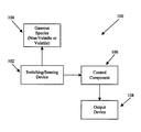
- FIG. 1 illustrates an example system 100 implementing the innovation.
- the system 100 may be a system where the exposure of a volatile or toxic gas may be harmful to humans and/or critical equipment.
- Some example systems may include airports and mass transportation systems, airplanes, and space platforms that require emissions monitoring, leak detection, engine monitoring, security, fire detection, personal health monitoring, environmental monitoring, etc.
- the system 100 includes a dual function nano-switching/sensing device 102 , a gaseous species 104 introduced to the nano-switching/sensing device 102 , a control component 106 , and an output device 108 .
- the nano-switching/sensing device 102 is a graphene-based nano-Switch/Sensor Schottky Diode (nanoSSSD) and will be described in more detail further below in reference to FIGS. 2, 3 (A), and 3 (B).
- the control component 106 receives information from the nano-switching/sensing device 102 and outputs a signal to the output device 108 .
- the nano-switching/sensing device 102 senses a gaseous species 104
- the switching portion of the nano-switching/sensing device 102 can automatically actuate thereby sending a signal to the control component 106 .
- the control component 106 in turn can activate the output device 108 , which may be in the form of a warning device.
- FIG. 2 illustrates a process 200 to fabricate a nanostructure device 300 , shown schematically in FIG. 3A , incorporating the nano-switching/sensing device 102 .
- a wafer is provided in the form of a single crystal, such as silicon (Si), to form a substrate 302 .
- a doping agent or dopant is added to the substrate 302 .
- the doping agent may be either an n-type (donor) or a p-type (acceptor) dopant. It should be noted that the responsiveness of the nanostructure device 300 differs depending on the substrate doping type.
- an insulator 304 is formed on the substrate 302 .
- the substrate is an n-type or a p-type doped silicon (Si) substrate and the insulator 304 is a thermally grown layer of silicon dioxide (SiO 2 ).
- the silicon resistivity of the doped silicon substrate 302 is on the order of 1-10 ohms per centimeter.
- the thickness of the SiO 2 insulating layer 304 has a thickness of approximately 100-300 nm.
- the nanoSSSD is only modestly impacted by oxide thickness and can operate over a wider range of oxide thickness than listed above. Fabrication of the nanostructure device 300 utilizing a silicon-based substrate enhances its compatibility with other silicon-based nanostructures.
- a pattern of electrodes 306 are formed on the substrate 302 using microfabrication techniques (e.g., sputter deposition, etc.).
- the electrodes 306 are gold (Au) electrodes and are disposed on the substrate 302 in a square checker-board type pattern. In other example embodiments, however, the electrodes 306 may be formed on the substrate 302 in any type of pattern (e.g., circular, rectangular, etc.).
- Graphene 308 is deposited on a top surface 310 of each electrode 306 and extends over an edge 312 of the electrode 306 so as to contact the substrate 302 , illustrated in FIGS. 3A and 3B .
- the graphene 308 provides a conductive path between the electrode 306 and the substrate 302 , thus forming the nanostructure device 300 and more specifically, a Schottky diode.
- the graphene 308 may include a single layer of graphene or multiple layers of graphene. Further, the graphene 308 may be produced by microfabrication techniques (e.g., exfoliation methods, chemical vapor deposition, etc.).
- the graphene 308 is formed on the top surface 310 of at least two electrodes 306 and a semiconducting region, which includes a portion of the substrate 302 and the insulator 304 , between the at least two electrodes 306 .
- graphene 308 is sensitive to the adsorption and desorption of a single gas molecule.
- the semiconducting region which includes the substrate 302 and/or the insulator 304 , may be etched such that the gaseous species to be sensed has direct physical access to both a top and bottom surface of the graphene 308 .
- FIGS. 4 and 5 represent micro-images of the nanostructure 300 .
- FIG. 4 is a top optical view microscopic image magnified 200 times of an actual graphene layer crossing the edge of the substrate 302 .
- FIG. 5 is a micrograph that illustrates the contact of the graphene layer 308 with the electrode 306 , which is disposed on the SiO 2 insulating layer 304 .
- a dc voltage may be applied between the electrode 306 and the substrate 302 to thereby activate of the nanostructure device 300 .
- the resulting I-V (Current-Voltage) characteristics of the nanostructure device 300 are illustrated in FIGS. 7-10 .
- a volatile species e.g., ammonia (NH 3 )
- the response is unambiguously different to that manifested under normal ambient conditions.
- FIG. 6 shows the experimental I-V characteristic response of the nanostructrure device 300 for the n-type doped silicon substrate 302 when the atmosphere is changed from a non-volatile species (e.g., nitrogen (N 2 )) to a volatile species (NH 3 ).
- FIG. 8 illustrates the experimental I-V characteristic response of the nanostructure 300 for the p-type doped silicon substrate 302 when the atmosphere is changed from the non-volatile species (N 2 ) to the volatile species (NH 3 ).
- a non-volatile species e.g., nitrogen (N 2 )
- NH 3 volatile species
- FIGS. 6 and 7 illustrate how the nanostructure device 300 responds when the nanostructure device 300 is exposed to a volatile species. Also significant, however, is the behavior of the nanostructure device 300 (shown in FIGS. 8 and 9 ) when the volatile species is removed. Specifically, as illustrated in FIGS. 8 and 9 , the performance of the nanostructure device 300 returns to its normal mode of operation as the volatile species is removed.
- I-V characteristics of the nanostructure device 300 when the volatile gaseous species NH 3 is introduced into an ambient atmosphere As the volatile species NH 3 is introduced, the I-V curve shifts to the left. Specifically, prior the introduction of the NH 3 , the I-V curve is represented by the purple line. As the NH 3 is introduced the I-V curve gradually shifts to the left and is represented by the yellow line.
- the I-V curve shifts to the right. Specifically, prior to the removal of the NH 3 , the I-V curve is represented by the dark blue line. As the NH 3 is introduced the I-V curve gradually shifts to the right and is represented by the light blue line.
- the performance of the nanostructure device 300 returns to its normal mode of operation as the volatile species is removed.
- This reversible feature forms the basis for the functional operation of the nanostructure device 300 , thus, resulting in a reliable, long mean-time-before-failure (MTBF) nano-switch/sensor that is ideal for applications where frequent replacement of the nanostructure device 300 is not a viable option.
- the nanostructure device 300 could act as a switch whose performance could be tailored by dispensing or retrieving the particulates of the volatile species.
- the innovation discussed here is unique not only because of the use of graphene, but also because of the fully reversible (i.e., reusable) dual nature of the nanostructure device 300 (i.e., nano-switch/sensor).
- the innovation presented in this disclosure has many unique and novel features.
- the nanostructure device 300 is based on a use of graphene to develop such a diode at the nanoscale.
- the nanostructure device 300 is extremely reliable, e.g., even under a harsh environment (i.e., human body internal environment; extreme cold/hot temperature environments; etc.).
- the innovation contrary to conventional nanosensors, which rely on cantilevers and other mechanical/moving parts, the innovation has no moving parts and, as such, promises to offer reliable performance with a long MTBF.
- the innovation exhibits dual use functionality. Specifically, the device can function as a sensor and a switch.
- the device can be fabricated using either n-doped or p-doped silicon, which adds another dimension for applications of the device by enhancing its compatibility with other silicon-based nanoelectronic circuits.
- the innovation is based on a vertical configuration, which saves highly wished circuit area, but may also be based on other configurations.
- the fabrication procedure is economical and therefore offers the possibility of low cost implementation when compared to traditional approaches.
- the innovation described herein has many potential commercial applications beyond those of traditional devices. For example, research groups have attempted to demonstrate a graphene-based switch with potential for applications in the non-volatile memory market. The device, however, functions only as a switch. In other words, unlike the innovation described herein, the conventional device does not exhibit sensing functions. Further, others have demonstrated, what they claim to be, the world's fastest graphene transistor operational at 26 GHz. This non-silicon based device, however, is not capable of both sensing and switching applications.
- the innovation described herein has the potential to expand the applications of combined switching/sensing graphene based nanoelectronics not only in areas ranging from embedded biomedical devices but also to extremely sensitive detection/switching devices required for earth or space-bound applications on harsh environment (e.g., airplanes turbines; surveillance of airports and mass transportation systems such as subways and trains; space platforms such as the International Space Station (ISS), Crew Exploration Vehicles (CEV), lunar and planetary habitats, etc.).
- harsh environment e.g., airplanes turbines; surveillance of airports and mass transportation systems such as subways and trains; space platforms such as the International Space Station (ISS), Crew Exploration Vehicles (CEV), lunar and planetary habitats, etc.
- Specific potential applications of the innovation include the detection of toxic gases such as ammonia, hydrogen, hydrocarbons, nitrogen oxides (NO x ) (i.e., NO and NO 2 ), carbon monoxide (CO), and carbon dioxide CO 2 .
- toxic gases such as ammonia, hydrogen, hydrocarbons, nitrogen oxides (NO x ) (i.e., NO and NO 2 ), carbon monoxide (CO), and carbon dioxide CO 2 .
- this device can be used to detect explosives, e.g., in an effort to prevent terrorist attacks.
- the device can detect 2,4-dinitrotoluene, which is a volatile material found in TNT explosives.
- the innovation can be connected to a visual and sound alarm that will be autonomously triggered in the presence of gas and return to its passive mode in absent of it. Further, the device can respond differently to each gas and, therefore, may be possible to generate colored signals, for example, where colors correspond to a specific detected gas.
- a conducting polymer nanofiber as the active element in the nanoSSSD device is further described in addition to the above.
- This conducting polymer nanofiber will replace at least one graphene layer mentioned in the above specifications without degradation of device performance.
- FIGS. 10, 11 and 12 show the device construction, and the external electrical connections.
- FIG. 13 shows the device current-voltage curves in the presence and absence of ammonia vapor. The operation is not affected and the device returns to original operating specifications.
Abstract
A nanostructure device is provided and performs dual functions as a nano-switching/sensing device. The nanostructure device includes a doped semiconducting substrate, an insulating layer disposed on the doped semiconducting substrate, an electrode formed on the insulating layer, and at least one polymer nanofiber deposited on the electrode. The at least one polymer nanofiber provides an electrical connection between the electrode and the substrate and is the electroactive element in the device.
Description
This Application is a continuation-in-part of co-pending U.S. patent application Ser. No. 13/242,300, entitled “Graphene Based Reversible Nano-Switch/Sensor Schottky Diode (nanoSSSD) Device”, filed on Sep. 23, 2011, and Issuance is pending.
The invention described herein was made by an employee of the United States Government and may be manufactured and used only by or for the Government for Government purposes without the payment of any royalties thereon or therefore.
Developing technologies in support of monitoring the health of astronauts and the operation of critical instrumentation are ongoing in order to develop a better understanding of the changes in the human body and equipment anticipated in future space exploration. Accordingly, the emergence of promising technologies such as nanotechnology has sparked efforts to develop operational electronic and sensing devices at the nanoscale level with performance and sensing resolutions not yet achieved. These efforts have resulted in great specificity attained by tailoring the surface of sensors (i.e., surface modification) by optical, chemical and physical means (i.e., via the creation of preferred end-groups using approaches such as self-assembled monolayers).
One key or unique issue with these approaches is that sensing takes place via the attachment of molecules of the desired species to the sensor end groups bringing it into an irreversible saturated state via physical adsorption or chemical adsorption. More importantly, in most instances, the nature of the sensor is such that its mean-time-before-failure (MTBF) is limited (e.g., sensors that are cantilever-based or any other rendition that contains moving parts). This poses a reliability concern especially when working with embedded sensors such as BioMEMS sensors, or sensors intended for remote, difficult to access locations such as spacecraft or robotic probes for planetary exploration.
Traditional approaches for developing state-of-the-art sensing technologies targeted for specific applications are costly, mostly due to the expensive laboratory and facilities infrastructure required for their fabrication and high-volume production. In addition, the hybrid integrated approach of the different circuit components makes size reduction difficult. Reduced size is a relevant requirement in applications such as Bio-embedded devices. Traditionally, even those sensing devices developed at the nanostructure level perform only a unifunctional, specific sensing task and not a dual switching/sensing function. Switching enables the device to autonomously respond to changes in normal conditions and trigger appropriate responses, and then revert to baseline operation once the environment being sensed has returned to normal.
For this dual functionality, the current state of the art on nano-switch/sensors are based on metal oxide components (e.g., ZnO) with circuits consisting of mechanical actuators such as cantilevers, which include many non-trivial fabrication steps. Furthermore, the mechanical nature of these conventional sensors limits reliability due to a reduction on the MTBF. This level of complexity may be a critical disadvantage that can hinder the transition of the device from laboratory demonstration to practical working applications.
The following presents a simplified summary in order to provide a basic understanding of some aspects of the innovation. This summary is not an extensive overview of the innovation. It is not intended to identify key/critical elements or to delineate the scope of the innovation. Its sole purpose is to present some concepts of the innovation in a simplified form as a prelude to the more detailed description that is presented later.
The innovation disclosed and claimed herein, in one aspect thereof, comprises a nanostructure device adapted to perform dual functions as a nano-switching/sensing device. The device includes a doped substrate, an insulating layer disposed on the substrate (e.g. silicon substrate), an electrode formed on the insulating layer, and at least one layer of graphene formed on the electrode. At least one layer of graphene provides an electrical connection between the electrode and the substrate and is the electroactive element in the device.
In another aspect of the innovation, the nanostructure device is based on a use of graphene to develop a diode at the nanoscale level.
In yet another aspect of the innovation, based on experimental performance of the nanostructure device, the innovation exhibits dual use functionality (e.g., switching and sensing) and reversibility characteristics.
In still another aspect of the innovation, the nanostructure device can be fabricated using either n-doped or p-doped silicon substrate, which adds another dimension for applications of the device by enhancing its compatibility with other silicon-based nanoelectronic circuits.
In yet another aspect, the innovation has no moving parts, which is contrary to conventional nanosensors that rely on cantilevers and other mechanical/moving parts. As a result, the innovation offers reliable performance with a long mean-time-before-failure (MTBF).
To accomplish the foregoing and related ends, certain illustrative aspects of the innovation are described herein in connection with the following description and the annexed drawings. These aspects are indicative, however, of but a few of the various ways in which the principles of the innovation can be employed and the subject innovation is intended to include all such aspects and their equivalents. Other advantages and novel features of the innovation will become apparent from the following detailed description of the innovation when considered in conjunction with the drawings.
In addition, there is no reported work on a graphene-based dual use nano-switch/sensor device for toxic gases. Consequently, the innovation reported in this disclosure represents the first proof of concept of that possibility.
The innovation is now described with reference to the drawings, wherein like reference numerals are used to refer to like elements throughout. In the following description, for purposes of explanation, numerous specific details are set forth in order to provide a thorough understanding of the subject innovation. It may be evident, however, that the innovation can be practiced without these specific details.
While specific characteristics are described herein (e.g., thickness), it is to be understood that the features, functions and benefits of the innovation can employ characteristics that vary from those described herein. These alternatives are to be included within the scope of the innovation and claims appended hereto.
Further, in view of the aspects and features described, methodologies that may be implemented in accordance with embodiments of the subject innovation will be better appreciated with reference to the figures. While for purposes of simplicity of explanation, the methodologies are shown and described as a series of drawings representing steps or acts associated with the methodologies, it is to be understood and appreciated that the claimed subject matter is not limited by the order of the drawings, as some drawings may occur concurrently with other drawings and/or in different orders than what is depicted and described herein. Where non-sequential, or branched, flow is illustrated via flowchart, it can be appreciated that various other branches, flow paths, and orders of the blocks, may be implemented which achieve the same or a similar result. Moreover, not all illustrated drawings may be required to implement the methodologies described hereinafter.
The innovation described herein and shown in the figures, in one aspect thereof, is representative of a nanostructure that may be a dual use nano-switching/sensing device comprised of a graphene-based nano-Schottky diode. The performance of the innovation has been experimentally tested in an ambient atmosphere as well as under other non-volatile and volatile atmospheres. For example, the innovation has been experimentally tested under ammonia gas (NH3), but could operate under other volatile or toxic gases, such as hydrogen, hydrocarbons, nitrogen oxides, carbon monoxide, carbon dioxide, etc. The resulting experimental data disclosed herein, demonstrates a dual switching/sensing nature (and function) of the innovation. Hence, the acronym nanoSSSD (nano-Switch/Sensor Schottky Diode). Further, the resulting experimental data also reveals a reversible characteristic of the innovation, which makes it suitable for nanosensing applications where access to the sensor and its potential replacement opportunities are limited (e.g., biosensors, harsh environment, etc.).
Specifically, due to the following characteristics of graphene, the innovation has extreme sensitivity to different gaseous species with a remarkable attribute of having reversibility properties, thereby serving as a building block for a volatile species sensor. As is known, graphene is formed from a single layer (one atom thick) of carbon and has a hexagonal shape. Thus, graphene is a 2-dimensional material and, as such, its entire volume is exposed to its surroundings, thereby making it sensitive to the adsorption and desorption of a single gas molecule. Further, graphene's single layer structure makes graphene a zero-gap semiconductor, where the valence band and the conduction band overlap, thereby giving graphene superior electrical conduction and low electrical noise properties. This high electrical conductance also contributes to graphene's sensitivity to the adsorption and desorption of a single gas molecule. Because graphene is sensitive to the adsorption and desorption of gas molecules, the resistivity of graphene also changes, thereby giving the graphene-based innovation its sensing ability. Therefore, the innovation, when operating as a sensor, is able to cycle between active and passive sensing states in response to the presence or absence, respectively, of the gaseous species. Furthermore, graphite is a three-dimensional material that is derived from stacking multiple layers of graphene. The electrical properties of thin layers of graphite will more closely resembled the electrical properties of graphene than those of thick graphite layers. The advantages of using graphite for the present invention include ease of fabrication and compatibility with standard semiconductor device processing techniques. Hence, the current device uses graphite as the sensing element as well as graphene.
In addition, because of the aforementioned sensitivity and diode properties, the device can be used as a switch whose operational stages (i.e., open/close or on/off) could be controlled by a given gaseous species. Consequently, the innovation has great potential as a building block for implementation of a switch/sensor device for harsh, embedded or enclosed environments (e.g., human body, space-based habitats, aircraft, rail, etc.) where the longevity and reusability of the circuit are critical for reliable operation. Furthermore, graphene's excellent electrical and physical properties such as the ability to maintain current densities approximately a million times higher than that of copper, record strength of 200 times greater than steel, and elastic stretching capabilities of up to 20%, will make this device more robust than those made from nano-cantilevers comprised of more fragile metal oxides.
With reference now to the figures, FIG. 1 illustrates an example system 100 implementing the innovation. The system 100 may be a system where the exposure of a volatile or toxic gas may be harmful to humans and/or critical equipment. Some example systems may include airports and mass transportation systems, airplanes, and space platforms that require emissions monitoring, leak detection, engine monitoring, security, fire detection, personal health monitoring, environmental monitoring, etc. The system 100 includes a dual function nano-switching/sensing device 102, a gaseous species 104 introduced to the nano-switching/sensing device 102, a control component 106, and an output device 108.
The nano-switching/sensing device 102 is a graphene-based nano-Switch/Sensor Schottky Diode (nanoSSSD) and will be described in more detail further below in reference to FIGS. 2, 3 (A), and 3(B). The control component 106 receives information from the nano-switching/sensing device 102 and outputs a signal to the output device 108. For example, if the nano-switching/sensing device 102 senses a gaseous species 104, the switching portion of the nano-switching/sensing device 102 can automatically actuate thereby sending a signal to the control component 106. The control component 106 in turn can activate the output device 108, which may be in the form of a warning device.
With reference to FIGS. 2, 3A, and 3B simultaneously, FIG. 2 illustrates a process 200 to fabricate a nanostructure device 300, shown schematically in FIG. 3A , incorporating the nano-switching/sensing device 102. At step 202, a wafer is provided in the form of a single crystal, such as silicon (Si), to form a substrate 302. At step 204, a doping agent or dopant is added to the substrate 302. The doping agent may be either an n-type (donor) or a p-type (acceptor) dopant. It should be noted that the responsiveness of the nanostructure device 300 differs depending on the substrate doping type. At step 206, an insulator 304 is formed on the substrate 302. In an example embodiment, the substrate is an n-type or a p-type doped silicon (Si) substrate and the insulator 304 is a thermally grown layer of silicon dioxide (SiO2). In the example embodiment, the silicon resistivity of the doped silicon substrate 302 is on the order of 1-10 ohms per centimeter. Further, the thickness of the SiO2 insulating layer 304 has a thickness of approximately 100-300 nm. However, the nanoSSSD is only modestly impacted by oxide thickness and can operate over a wider range of oxide thickness than listed above. Fabrication of the nanostructure device 300 utilizing a silicon-based substrate enhances its compatibility with other silicon-based nanostructures.
At step 208, a pattern of electrodes 306 are formed on the substrate 302 using microfabrication techniques (e.g., sputter deposition, etc.). In an example embodiment shown in FIGS. 4-5 , the electrodes 306 are gold (Au) electrodes and are disposed on the substrate 302 in a square checker-board type pattern. In other example embodiments, however, the electrodes 306 may be formed on the substrate 302 in any type of pattern (e.g., circular, rectangular, etc.).
In another example embodiment, the graphene 308 is formed on the top surface 310 of at least two electrodes 306 and a semiconducting region, which includes a portion of the substrate 302 and the insulator 304, between the at least two electrodes 306. As mentioned above, graphene 308 is sensitive to the adsorption and desorption of a single gas molecule. In an example embodiment, the semiconducting region, which includes the substrate 302 and/or the insulator 304, may be etched such that the gaseous species to be sensed has direct physical access to both a top and bottom surface of the graphene 308.
Referring again to FIG. 3A , a dc voltage may be applied between the electrode 306 and the substrate 302 to thereby activate of the nanostructure device 300. The resulting I-V (Current-Voltage) characteristics of the nanostructure device 300 are illustrated in FIGS. 7-10 . As illustrated, when the nanostructure device 300 is exposed to a volatile species (e.g., ammonia (NH3)), the response (diode response) is unambiguously different to that manifested under normal ambient conditions.
Specifically, FIG. 6 shows the experimental I-V characteristic response of the nanostructrure device 300 for the n-type doped silicon substrate 302 when the atmosphere is changed from a non-volatile species (e.g., nitrogen (N2)) to a volatile species (NH3). Similarly, FIG. 8 illustrates the experimental I-V characteristic response of the nanostructure 300 for the p-type doped silicon substrate 302 when the atmosphere is changed from the non-volatile species (N2) to the volatile species (NH3).
As described above, FIGS. 6 and 7 illustrate how the nanostructure device 300 responds when the nanostructure device 300 is exposed to a volatile species. Also significant, however, is the behavior of the nanostructure device 300 (shown in FIGS. 8 and 9 ) when the volatile species is removed. Specifically, as illustrated in FIGS. 8 and 9 , the performance of the nanostructure device 300 returns to its normal mode of operation as the volatile species is removed.
Referring to FIG. 8 , illustrated are I-V characteristics of the nanostructure device 300 when the volatile gaseous species NH3 is introduced into an ambient atmosphere. As the volatile species NH3 is introduced, the I-V curve shifts to the left. Specifically, prior the introduction of the NH3, the I-V curve is represented by the purple line. As the NH3 is introduced the I-V curve gradually shifts to the left and is represented by the yellow line.
Conversely, referring to FIG. 9 , illustrated are I-V characteristics of the nanostructure device 300 with the removal of the volatile gaseous species NH3 and the atmosphere returns to the ambient atmosphere. As the volatile species NH3 is removed, the I-V curve shifts to the right. Specifically, prior to the removal of the NH3, the I-V curve is represented by the dark blue line. As the NH3 is introduced the I-V curve gradually shifts to the right and is represented by the light blue line.
As clearly illustrated by FIGS. 8 and 9 and as indicated above, the performance of the nanostructure device 300 returns to its normal mode of operation as the volatile species is removed. This reversible feature forms the basis for the functional operation of the nanostructure device 300, thus, resulting in a reliable, long mean-time-before-failure (MTBF) nano-switch/sensor that is ideal for applications where frequent replacement of the nanostructure device 300 is not a viable option. In addition, based on the same feature, the nanostructure device 300 could act as a switch whose performance could be tailored by dispensing or retrieving the particulates of the volatile species.
While, as discussed above, there are other alternate approaches for attaining nanosensors, the innovation discussed here is unique not only because of the use of graphene, but also because of the fully reversible (i.e., reusable) dual nature of the nanostructure device 300 (i.e., nano-switch/sensor). As a result, the innovation presented in this disclosure has many unique and novel features. First, the nanostructure device 300 is based on a use of graphene to develop such a diode at the nanoscale. Second, because of the properties of graphene (i.e., maximization of sensing surface due to 2-dimensional nature, robustness, good electrical conductivity, etc.) the nanostructure device 300 is extremely reliable, e.g., even under a harsh environment (i.e., human body internal environment; extreme cold/hot temperature environments; etc.). Third, contrary to conventional nanosensors, which rely on cantilevers and other mechanical/moving parts, the innovation has no moving parts and, as such, promises to offer reliable performance with a long MTBF. Fourth, based on the performance of the device, the innovation exhibits dual use functionality. Specifically, the device can function as a sensor and a switch. Fifth, the device can be fabricated using either n-doped or p-doped silicon, which adds another dimension for applications of the device by enhancing its compatibility with other silicon-based nanoelectronic circuits. Sixth, the innovation is based on a vertical configuration, which saves highly coveted circuit area, but may also be based on other configurations. Seventh, the fabrication procedure is economical and therefore offers the possibility of low cost implementation when compared to traditional approaches.
The aforementioned functionalities can be either exploited separately or in tandem depending on the specific application, which adds to the versatility of the device. Specifically, the innovation described herein has many potential commercial applications beyond those of traditional devices. For example, research groups have attempted to demonstrate a graphene-based switch with potential for applications in the non-volatile memory market. The device, however, functions only as a switch. In other words, unlike the innovation described herein, the conventional device does not exhibit sensing functions. Further, others have demonstrated, what they claim to be, the world's fastest graphene transistor operational at 26 GHz. This non-silicon based device, however, is not capable of both sensing and switching applications.
The innovation described herein, on the other hand, has the potential to expand the applications of combined switching/sensing graphene based nanoelectronics not only in areas ranging from embedded biomedical devices but also to extremely sensitive detection/switching devices required for earth or space-bound applications on harsh environment (e.g., airplanes turbines; surveillance of airports and mass transportation systems such as subways and trains; space platforms such as the International Space Station (ISS), Crew Exploration Vehicles (CEV), lunar and planetary habitats, etc.).
Specific potential applications of the innovation include the detection of toxic gases such as ammonia, hydrogen, hydrocarbons, nitrogen oxides (NOx) (i.e., NO and NO2), carbon monoxide (CO), and carbon dioxide CO2.
In addition, this device can be used to detect explosives, e.g., in an effort to prevent terrorist attacks. For example, the device can detect 2,4-dinitrotoluene, which is a volatile material found in TNT explosives.
In yet other aspects, the innovation can be connected to a visual and sound alarm that will be autonomously triggered in the presence of gas and return to its passive mode in absent of it. Further, the device can respond differently to each gas and, therefore, may be possible to generate colored signals, for example, where colors correspond to a specific detected gas.
In yet another embodiment, the use of a conducting polymer nanofiber as the active element in the nanoSSSD device is further described in addition to the above. This conducting polymer nanofiber will replace at least one graphene layer mentioned in the above specifications without degradation of device performance.
The innovation described retains all of the aspects of the previous innovation with the additional possibility that this device can also be used to detect UV radiation. Conducting polymers are sensitive to UV radiation via the creation of electron-hole pairs that subsequently interact with adsorbed atoms or molecules on the polymer. In the case of a nanofiber that has an extremely high surface area to volume ratio such interaction can occur at extremely low concentrations which implies a very low detection threshold for UV radiation.
What has been described above includes examples of the innovation. It is, of course, not possible to describe every conceivable combination of components or methodologies for purposes of describing the subject innovation, but one of ordinary skill in the art may recognize that many further combinations and permutations of the innovation are possible. Accordingly, the innovation is intended to embrace all such alterations, modifications and variations that fall within the spirit and scope of the appended claims. Furthermore, to the extent that the term “includes” is used in either the detailed description or the claims, such term is intended to be inclusive in a manner similar to the term “comprising” as “comprising” is interpreted when employed as a transitional word in a claim.
Claims (20)
1. A nanostructure device comprising:
a doped semiconducting substrate;
an insulating layer disposed on the doped semiconducting substrate;
an electrode formed on the insulating layer; and
at least one polymer nanofiber deposited on the electrode and providing an electrical connection between the electrode and the substrate, wherein the nanostructure device is adapted to perform dual functions as a nano-switching/sensing device.
2. The nanostructure device of claim 1 , wherein the at least one polymer nanofiber deposited on a top surface of the electrode and extends over an edge of the electrode and contacts the doped substrate to thereby form a Schottky or a p-n junction diode.
3. The nanostructure device of claim 2 , wherein when the dual function nano-switching/sensing device is exposed to a volatile gaseous species, the at least one polymer nanofiber adsorbs at least one molecule of the volatile gaseous species thereby altering an operation of the dual function nano-switching/sensing device to allow the nano-switching/sensing device to detect the presence of the volatile gaseous species.
4. The nanostructure device of claim 3 , wherein when nano-switching/sensing device is removed from the volatile gaseous species, the at least one molecule of the volatile gaseous species is desorbed from the at least one polymer nanofiber and the nano-switching/sensing device returns to a normal mode of operation to thereby allow the nano-switching/sensing device to detect the absence of the volatile gaseous species.
5. The nanostructure device of claim 3 , wherein when the dual function nano-switching/sensing device is exposed to ultra-violet irradiation, the at least one polymer nanofiber adsorbs at least one photon thereby altering an operation of the dual function nano-switching/sensing device to allow the nano-switching/sensing device to detect the presence of the radiation.
6. The nanostructure device of claim 5 , wherein when nano-switching/sensing device is removed from the ultra-violet irradiation, the at least one photon of the radiation is emitted from the at least one polymer nanofiber and the nano-switching/sensing device returns to a normal mode of operation to thereby allow the nano-switching/sensing device to detect the absence of the radiation.
7. The nanostructure device of claim 1 , wherein the doped substrate is a silicon substrate doped with an n-type doping agent and has a silicon resistivity in the range of 1-10 ohms-centimeter.
8. The nanostructure device of claim 1 , wherein the doped substrate is a silicon substrate doped with a p-type doping agent and has a silicon resistivity in the range of 1-10 ohms-centimeter.
9. The nanostructure device of claim 1 , wherein the insulating layer is a silicon dioxide layer having a thickness of approximately 100-300 nm.
10. The nanostructure device of claim 1 , wherein the electrode is an electrically conductive electrode.
11. The nanostructure device of claim 1 , wherein when the Schottky or p-n junction diode is exposed to a gaseous volatile species, I-V characteristics of the Schottky or p-n junction diode are altered such that the Schottky or p-n junction diode detects the presence of the volatile gaseous species, and wherein when the Schottky or p-n junction diode is removed from the volatile gaseous species, the I-V characteristics of the Schottky or a p-n junction diode reverse and return to their normal mode of operation such that the Schottky or a p-n junction diode detects the absence of the volatile gaseous species.
12. The nanostructure device of claim 1 , wherein when the Schottky or p-n junction diode is exposed to ultra-violet radiation, I-V characteristics of the Schottky or p-n junction diode are altered such that the Schottky or p-n junction diode detects the presence of the radiation, and wherein when the Schottky or p-n junction diode is removed from the radiation, the I-V characteristics of the Schottky or a p-n junction diode reverse and return to their normal mode of operation such that the Schottky or a p-n junction diode detects the absence of the radiation.
13. The nanostructure device of claim 1 , wherein the doped substrate is a silicon substrate doped with an n-type doping agent and has a silicon resistivity in the range of 1-10 ohms-centimeter.
14. The nanostructure device of claim 1 , wherein the doped substrate is a silicon substrate doped with a p-type doping agent and has a silicon resistivity in the range of 1-10 ohms-centimeter.
15. The nanostructure device of claim 1 , wherein the insulating layer is a silicon dioxide layer having a thickness of approximately 100-300 nm.
16. The nanostructure device of claim 1 , wherein the electrode is an electrically conducting electrode.
17. The nanostructure device of claim 1 , wherein the electrode formed on the insulating layer comprises at least two electrodes, wherein the at least one polymer nanofiber deposited on a top surface of the at least two electrodes and a semiconducting region between the at least two electrodes, and wherein a portion of the semiconducting region is etched such that a gaseous species to be sensed has direct physical access to both a top surface and a bottom surface of the at least one polymer nanofiber.
18. The nanostructure device of claim 1 , wherein the electrode formed on the insulating layer comprises at least two electrodes, wherein the at least one polymer nanofiber deposited on a top surface of the at least two electrodes and a semiconducting region between the at least two electrodes, and wherein a portion of the semiconducting region is etched such that ultra-violet radiation to be sensed has direct physical access to both a top surface and a bottom surface of the at least one polymer nanofiber.
19. The nanostructure device of claim 1 , wherein when the dual function nano-switching/sensing device is exposed to a volatile gaseous species, the at least one polymer nanofiber adsorbs at least one molecule of the volatile gaseous species thereby altering an operation of the dual function nano-switching/sensing device to allow the nano-switching/sensing device to detect the presence of the volatile gaseous species, and wherein when nano-switching/sensing device is removed from the volatile gaseous species, the at least one molecule of the volatile gaseous species is desorbed from the at least one polymer nanofiber and the nano-switching/sensing device returns to a normal mode of operation to thereby allow the nano-switching/sensing device to detect the absence of the volatile gaseous species.
20. The nanostructure device of claim 1 , wherein when the dual function nano-switching/sensing device is exposed to ultra-violet radiation, the at least one polymer nanofiber adsorbs at least one photon of the radiation thereby altering an operation of the dual function nano-switching/sensing device to allow the nano-switching/sensing device to detect the presence of the radiation, and wherein when nano-switching/sensing device is removed from the radiation, the at least one photon of the radiation is emitted from the at least one polymer nanofiber and the nano-switching/sensing device returns to a normal mode of operation to thereby allow the nano-switching/sensing device to detect the absence of the radiation.
Priority Applications (2)
| Application Number | Priority Date | Filing Date | Title |
|---|---|---|---|
| US14/672,673 US9753001B1 (en) | 2011-09-23 | 2015-03-30 | Polymer nanofiber based reversible nano-switch/sensor diode (nanoSSSD) device |
| US15/655,498 US10067080B1 (en) | 2011-09-23 | 2017-07-20 | Polymer nanofiber based reversible nano-switch/sensor schottky diode (nanoSSSD) device |
Applications Claiming Priority (2)
| Application Number | Priority Date | Filing Date | Title |
|---|---|---|---|
| US13/242,300 US9016108B1 (en) | 2011-09-23 | 2011-09-23 | Graphene based reversible nano-switch/sensor Schottky diode (nanoSSSD) device |
| US14/672,673 US9753001B1 (en) | 2011-09-23 | 2015-03-30 | Polymer nanofiber based reversible nano-switch/sensor diode (nanoSSSD) device |
Related Parent Applications (1)
| Application Number | Title | Priority Date | Filing Date |
|---|---|---|---|
| US13/242,300 Continuation-In-Part US9016108B1 (en) | 2011-09-23 | 2011-09-23 | Graphene based reversible nano-switch/sensor Schottky diode (nanoSSSD) device |
Related Child Applications (1)
| Application Number | Title | Priority Date | Filing Date |
|---|---|---|---|
| US15/655,498 Continuation US10067080B1 (en) | 2011-09-23 | 2017-07-20 | Polymer nanofiber based reversible nano-switch/sensor schottky diode (nanoSSSD) device |
Publications (1)
| Publication Number | Publication Date |
|---|---|
| US9753001B1 true US9753001B1 (en) | 2017-09-05 |
Family
ID=59701452
Family Applications (2)
| Application Number | Title | Priority Date | Filing Date |
|---|---|---|---|
| US14/672,673 Active 2032-02-13 US9753001B1 (en) | 2011-09-23 | 2015-03-30 | Polymer nanofiber based reversible nano-switch/sensor diode (nanoSSSD) device |
| US15/655,498 Active US10067080B1 (en) | 2011-09-23 | 2017-07-20 | Polymer nanofiber based reversible nano-switch/sensor schottky diode (nanoSSSD) device |
Family Applications After (1)
| Application Number | Title | Priority Date | Filing Date |
|---|---|---|---|
| US15/655,498 Active US10067080B1 (en) | 2011-09-23 | 2017-07-20 | Polymer nanofiber based reversible nano-switch/sensor schottky diode (nanoSSSD) device |
Country Status (1)
| Country | Link |
|---|---|
| US (2) | US9753001B1 (en) |
Cited By (1)
| Publication number | Priority date | Publication date | Assignee | Title |
|---|---|---|---|---|
| WO2020100051A1 (en) * | 2018-11-13 | 2020-05-22 | Khalifa University of Science and Technology | Non-volatile memory systems based on single nanoparticles for compact and high data storage electronic devices |
Citations (28)
| Publication number | Priority date | Publication date | Assignee | Title |
|---|---|---|---|---|
| US20090174435A1 (en) | 2007-10-01 | 2009-07-09 | University Of Virginia | Monolithically-Integrated Graphene-Nano-Ribbon (GNR) Devices, Interconnects and Circuits |
| US20090235721A1 (en) | 2008-03-20 | 2009-09-24 | The Government Of The United States Of America, As Represented By The Secretary Of The Navy | Reduced graphene oxide film |
| US20090256130A1 (en) * | 2008-04-11 | 2009-10-15 | Sandisk 3D Llc | Memory cell that employs a selectively fabricated carbon nano-tube reversible resistance-switching element, and methods of forming the same |
| US20090278112A1 (en) * | 2008-04-11 | 2009-11-12 | Sandisk 3D Llc | Methods for etching carbon nano-tube films for use in non-volatile memories |
| US20090294759A1 (en) | 2008-05-29 | 2009-12-03 | Samsung Electronics Co., Ltd. | Stack structure comprising epitaxial graphene, method of forming the stack structure, and electronic device comprising the stack structure |
| US20100021708A1 (en) | 2008-04-14 | 2010-01-28 | Massachusetts Institute Of Technology | Large-Area Single- and Few-Layer Graphene on Arbitrary Substrates |
| US20100025660A1 (en) | 2008-07-31 | 2010-02-04 | University Of Connecticut | Semiconductor devices, methods of manufacture thereof and articles comprising the same |
| US20100055464A1 (en) | 2008-07-08 | 2010-03-04 | Chien-Min Sung | Graphene and Hexagonal Boron Nitride Planes and Associated Methods |
| US7719318B1 (en) | 2008-11-05 | 2010-05-18 | Sandia Corporation | Nanoeletromechanical switch and logic circuits formed therefrom |
| US20100140723A1 (en) | 2003-03-25 | 2010-06-10 | Kulite Semiconductor Products, Inc. | Nanotube and graphene semiconductor structures with varying electrical properties |
| US20100213435A1 (en) | 2009-02-24 | 2010-08-26 | Shosuke Fujii | Switching device and nonvolatile memory device |
| US7785557B2 (en) | 2006-06-13 | 2010-08-31 | Unidym, Inc. | Method of producing a graphene film as transparent and electrically conducting material |
| US20100218801A1 (en) | 2008-07-08 | 2010-09-02 | Chien-Min Sung | Graphene and Hexagonal Boron Nitride Planes and Associated Methods |
| US20100255984A1 (en) | 2009-04-03 | 2010-10-07 | Brookhaven Science Associates, Llc | Monolayer and/or Few-Layer Graphene On Metal or Metal-Coated Substrates |
| US20100327847A1 (en) | 2007-09-12 | 2010-12-30 | President And Fellows Of Harvard College | High-Resolution Molecular Sensor |
| US20110048625A1 (en) | 2009-08-27 | 2011-03-03 | Caldwell Joshua D | METHOD FOR THE REDUCTION OF GRAPHENE FILM THICKNESS AND THE REMOVAL AND TRANSFER OF EPITAXIAL GRAPHENE FILMS FROM SiC SUBSTRATES |
| US20110059599A1 (en) | 2009-09-10 | 2011-03-10 | Lockheed Martin Corporation | Graphene Nanoelectric Device Fabrication |
| US20110068320A1 (en) | 2009-09-21 | 2011-03-24 | Marinero Ernesto E | Quantum well graphene structure |
| US20110068290A1 (en) | 2008-05-30 | 2011-03-24 | The Regents Of The University Of California | Chemical modulation of electronic and magnetic properties of graphene |
| US20110089404A1 (en) | 2008-04-24 | 2011-04-21 | President And Fellows Of Harvard College | Microfabrication of Carbon-based Devices Such as Gate-Controlled Graphene Devices |
| US20110102068A1 (en) | 2009-10-30 | 2011-05-05 | The Regents Of The University Of California | Graphene device and method of using graphene device |
| US7944728B2 (en) | 2008-12-19 | 2011-05-17 | Sandisk 3D Llc | Programming a memory cell with a diode in series by applying reverse bias |
| US20130273708A1 (en) * | 2009-07-02 | 2013-10-17 | Heilongjiang University | Method of manufacturing a nanostructure quick-switch memristor |
| US20140213032A1 (en) * | 2013-01-31 | 2014-07-31 | Sandisk 3D Llc | Process For Forming Resistive Switching Memory Cells Using Nano-Particles |
| US20140262707A1 (en) * | 2013-03-14 | 2014-09-18 | Chytra Pawashe | Nanowire-based mechanical switching device |
| US20150079342A1 (en) * | 2013-01-14 | 2015-03-19 | California Institute Of Technology | Method and system for graphene formation |
| US9016108B1 (en) * | 2011-09-23 | 2015-04-28 | The United States Of America As Represented By The Administrator Of National Aeronautics And Space Administration | Graphene based reversible nano-switch/sensor Schottky diode (nanoSSSD) device |
| US20160223843A1 (en) * | 2013-09-02 | 2016-08-04 | Samsung Electronics Co., Ltd. | Tunable nano-antenna and methods of manufacturing and operating the same |
Family Cites Families (4)
| Publication number | Priority date | Publication date | Assignee | Title |
|---|---|---|---|---|
| WO2007015710A2 (en) * | 2004-11-09 | 2007-02-08 | Board Of Regents, The University Of Texas System | The fabrication and application of nanofiber ribbons and sheets and twisted and non-twisted nanofiber yarns |
| US7875090B2 (en) | 2007-04-24 | 2011-01-25 | The United States Of America As Represented By The Secretary Of Agriculture | Method and apparatus to protect synthesis gas via flash pyrolysis and gasification in a molten liquid |
| FR2931451B1 (en) | 2008-05-22 | 2010-12-17 | Fmc Technologies Sa | CONTROL DEVICE FOR SYSTEM FOR LOADING AND / OR UNLOADING FLUIDS |
| US8217723B2 (en) | 2009-11-05 | 2012-07-10 | Texas Instruments Incorporated | Low noise amplifier circuit |
-
2015
- 2015-03-30 US US14/672,673 patent/US9753001B1/en active Active
-
2017
- 2017-07-20 US US15/655,498 patent/US10067080B1/en active Active
Patent Citations (28)
| Publication number | Priority date | Publication date | Assignee | Title |
|---|---|---|---|---|
| US20100140723A1 (en) | 2003-03-25 | 2010-06-10 | Kulite Semiconductor Products, Inc. | Nanotube and graphene semiconductor structures with varying electrical properties |
| US7785557B2 (en) | 2006-06-13 | 2010-08-31 | Unidym, Inc. | Method of producing a graphene film as transparent and electrically conducting material |
| US20100327847A1 (en) | 2007-09-12 | 2010-12-30 | President And Fellows Of Harvard College | High-Resolution Molecular Sensor |
| US20090174435A1 (en) | 2007-10-01 | 2009-07-09 | University Of Virginia | Monolithically-Integrated Graphene-Nano-Ribbon (GNR) Devices, Interconnects and Circuits |
| US20090235721A1 (en) | 2008-03-20 | 2009-09-24 | The Government Of The United States Of America, As Represented By The Secretary Of The Navy | Reduced graphene oxide film |
| US20090256130A1 (en) * | 2008-04-11 | 2009-10-15 | Sandisk 3D Llc | Memory cell that employs a selectively fabricated carbon nano-tube reversible resistance-switching element, and methods of forming the same |
| US20090278112A1 (en) * | 2008-04-11 | 2009-11-12 | Sandisk 3D Llc | Methods for etching carbon nano-tube films for use in non-volatile memories |
| US20100021708A1 (en) | 2008-04-14 | 2010-01-28 | Massachusetts Institute Of Technology | Large-Area Single- and Few-Layer Graphene on Arbitrary Substrates |
| US20110089404A1 (en) | 2008-04-24 | 2011-04-21 | President And Fellows Of Harvard College | Microfabrication of Carbon-based Devices Such as Gate-Controlled Graphene Devices |
| US20090294759A1 (en) | 2008-05-29 | 2009-12-03 | Samsung Electronics Co., Ltd. | Stack structure comprising epitaxial graphene, method of forming the stack structure, and electronic device comprising the stack structure |
| US20110068290A1 (en) | 2008-05-30 | 2011-03-24 | The Regents Of The University Of California | Chemical modulation of electronic and magnetic properties of graphene |
| US20100055464A1 (en) | 2008-07-08 | 2010-03-04 | Chien-Min Sung | Graphene and Hexagonal Boron Nitride Planes and Associated Methods |
| US20100218801A1 (en) | 2008-07-08 | 2010-09-02 | Chien-Min Sung | Graphene and Hexagonal Boron Nitride Planes and Associated Methods |
| US20100025660A1 (en) | 2008-07-31 | 2010-02-04 | University Of Connecticut | Semiconductor devices, methods of manufacture thereof and articles comprising the same |
| US7719318B1 (en) | 2008-11-05 | 2010-05-18 | Sandia Corporation | Nanoeletromechanical switch and logic circuits formed therefrom |
| US7944728B2 (en) | 2008-12-19 | 2011-05-17 | Sandisk 3D Llc | Programming a memory cell with a diode in series by applying reverse bias |
| US20100213435A1 (en) | 2009-02-24 | 2010-08-26 | Shosuke Fujii | Switching device and nonvolatile memory device |
| US20100255984A1 (en) | 2009-04-03 | 2010-10-07 | Brookhaven Science Associates, Llc | Monolayer and/or Few-Layer Graphene On Metal or Metal-Coated Substrates |
| US20130273708A1 (en) * | 2009-07-02 | 2013-10-17 | Heilongjiang University | Method of manufacturing a nanostructure quick-switch memristor |
| US20110048625A1 (en) | 2009-08-27 | 2011-03-03 | Caldwell Joshua D | METHOD FOR THE REDUCTION OF GRAPHENE FILM THICKNESS AND THE REMOVAL AND TRANSFER OF EPITAXIAL GRAPHENE FILMS FROM SiC SUBSTRATES |
| US20110059599A1 (en) | 2009-09-10 | 2011-03-10 | Lockheed Martin Corporation | Graphene Nanoelectric Device Fabrication |
| US20110068320A1 (en) | 2009-09-21 | 2011-03-24 | Marinero Ernesto E | Quantum well graphene structure |
| US20110102068A1 (en) | 2009-10-30 | 2011-05-05 | The Regents Of The University Of California | Graphene device and method of using graphene device |
| US9016108B1 (en) * | 2011-09-23 | 2015-04-28 | The United States Of America As Represented By The Administrator Of National Aeronautics And Space Administration | Graphene based reversible nano-switch/sensor Schottky diode (nanoSSSD) device |
| US20150079342A1 (en) * | 2013-01-14 | 2015-03-19 | California Institute Of Technology | Method and system for graphene formation |
| US20140213032A1 (en) * | 2013-01-31 | 2014-07-31 | Sandisk 3D Llc | Process For Forming Resistive Switching Memory Cells Using Nano-Particles |
| US20140262707A1 (en) * | 2013-03-14 | 2014-09-18 | Chytra Pawashe | Nanowire-based mechanical switching device |
| US20160223843A1 (en) * | 2013-09-02 | 2016-08-04 | Samsung Electronics Co., Ltd. | Tunable nano-antenna and methods of manufacturing and operating the same |
Cited By (1)
| Publication number | Priority date | Publication date | Assignee | Title |
|---|---|---|---|---|
| WO2020100051A1 (en) * | 2018-11-13 | 2020-05-22 | Khalifa University of Science and Technology | Non-volatile memory systems based on single nanoparticles for compact and high data storage electronic devices |
Also Published As
| Publication number | Publication date |
|---|---|
| US10067080B1 (en) | 2018-09-04 |
Similar Documents
| Publication | Publication Date | Title |
|---|---|---|
| Soo et al. | Advances of SiC-based MOS capacitor hydrogen sensors for harsh environment applications | |
| Smith et al. | Graphene-based CO 2 sensing and its cross-sensitivity with humidity | |
| Popov et al. | Graphene-based humidity sensors: The origin of alternating resistance change | |
| Yang et al. | Hot carrier trapping induced negative photoconductance in InAs nanowires toward novel nonvolatile memory | |
| Stutzmann et al. | GaN-based heterostructures for sensor applications | |
| Kolmakov et al. | Chemical sensing and catalysis by one-dimensional metal-oxide nanostructures | |
| Yang et al. | Humidity sensing using vertically oriented arrays of ReS2 nanosheets deposited on an interdigitated gold electrode | |
| Katz | Chemically sensitive field‐effect transistors and chemiresistors: New materials and device structures | |
| Reddy et al. | Recent material advances and their mechanistic approaches for room temperature chemiresistive gas sensors | |
| Gao et al. | A DFT study of In doped Tl2O: a superior NO2 gas sensor with selective adsorption and distinct optical response | |
| Liu et al. | Building functional memories and logic circuits with 2D boron nitride | |
| US9016108B1 (en) | Graphene based reversible nano-switch/sensor Schottky diode (nanoSSSD) device | |
| US20100284156A1 (en) | Vertically-stacked electronic devices having conductive carbon films | |
| Swanwick et al. | Near-ultraviolet zinc oxide nanowire sensor using low temperature hydrothermal growth | |
| Chikkadi et al. | Advances in NO2 sensing with individual single-walled carbon nanotube transistors | |
| Wu et al. | Enhanced piezoresistive behavior of SiC nanowire by coupling with piezoelectric effect | |
| US10067080B1 (en) | Polymer nanofiber based reversible nano-switch/sensor schottky diode (nanoSSSD) device | |
| Bhattacharyya et al. | Impact of device configurations on sensing performance of WS 2-based gas sensors: A review | |
| Davydova et al. | Gas sensing properties of nanocrystalline diamond at room temperature | |
| Jang et al. | Palladium nanogap-based H2 sensors on a patterned elastomeric substrate using nanoimprint lithography | |
| CN111307876A (en) | Gas sensor for detecting nitrogen dioxide and preparation method thereof | |
| Pereira et al. | Reversible doping of graphene field effect transistors by molecular hydrogen: the role of the metal/graphene interface | |
| KR101997367B1 (en) | Conductive filament-based gas sensor and gas sensing method using the same | |
| Juang | Ag additive and nanorod structure enhanced gas sensing properties of metal oxide-based CO 2 sensor | |
| Jha et al. | Integrated nanorods and heterostructure field effect transistors for gas sensing |
Legal Events
| Date | Code | Title | Description |
|---|---|---|---|
| STCF | Information on status: patent grant |
Free format text: PATENTED CASE |
|
| MAFP | Maintenance fee payment |
Free format text: PAYMENT OF MAINTENANCE FEE, 4TH YEAR, LARGE ENTITY (ORIGINAL EVENT CODE: M1551); ENTITY STATUS OF PATENT OWNER: LARGE ENTITY Year of fee payment: 4 |