US9740976B2 - RFID tag and manufacturing method thereof - Google Patents

RFID tag and manufacturing method thereof Download PDF

Info

Publication number
US9740976B2
US9740976B2 US15/012,967 US201615012967A US9740976B2 US 9740976 B2 US9740976 B2 US 9740976B2 US 201615012967 A US201615012967 A US 201615012967A US 9740976 B2 US9740976 B2 US 9740976B2
Authority
US
United States
Prior art keywords
rfid tag
metal layer
dipole antenna
layer
core
Prior art date
Legal status (The legal status is an assumption and is not a legal conclusion. Google has not performed a legal analysis and makes no representation as to the accuracy of the status listed.)
Expired - Fee Related, expires
Application number
US15/012,967
Other versions
US20160155041A1 (en
Inventor
Noritsugu Ozaki
Shunji Baba
Takayoshi Matsumura
Current Assignee (The listed assignees may be inaccurate. Google has not performed a legal analysis and makes no representation or warranty as to the accuracy of the list.)
Fujitsu Ltd
Original Assignee
Fujitsu Ltd
Priority date (The priority date is an assumption and is not a legal conclusion. Google has not performed a legal analysis and makes no representation as to the accuracy of the date listed.)
Filing date
Publication date
Application filed by Fujitsu Ltd filed Critical Fujitsu Ltd
Assigned to FUJITSU LIMITED reassignment FUJITSU LIMITED ASSIGNMENT OF ASSIGNORS INTEREST (SEE DOCUMENT FOR DETAILS). Assignors: MATSUMURA, TAKAYOSHI, OZAKI, NORITSUGU, BABA, SHUNJI
Publication of US20160155041A1 publication Critical patent/US20160155041A1/en
Application granted granted Critical
Publication of US9740976B2 publication Critical patent/US9740976B2/en
Expired - Fee Related legal-status Critical Current
Adjusted expiration legal-status Critical

Links

Images

Classifications

    • GPHYSICS
    • G06COMPUTING; CALCULATING OR COUNTING
    • G06KGRAPHICAL DATA READING; PRESENTATION OF DATA; RECORD CARRIERS; HANDLING RECORD CARRIERS
    • G06K19/00Record carriers for use with machines and with at least a part designed to carry digital markings
    • G06K19/06Record carriers for use with machines and with at least a part designed to carry digital markings characterised by the kind of the digital marking, e.g. shape, nature, code
    • G06K19/067Record carriers with conductive marks, printed circuits or semiconductor circuit elements, e.g. credit or identity cards also with resonating or responding marks without active components
    • G06K19/07Record carriers with conductive marks, printed circuits or semiconductor circuit elements, e.g. credit or identity cards also with resonating or responding marks without active components with integrated circuit chips
    • G06K19/0723Record carriers with conductive marks, printed circuits or semiconductor circuit elements, e.g. credit or identity cards also with resonating or responding marks without active components with integrated circuit chips the record carrier comprising an arrangement for non-contact communication, e.g. wireless communication circuits on transponder cards, non-contact smart cards or RFIDs
    • GPHYSICS
    • G06COMPUTING; CALCULATING OR COUNTING
    • G06KGRAPHICAL DATA READING; PRESENTATION OF DATA; RECORD CARRIERS; HANDLING RECORD CARRIERS
    • G06K19/00Record carriers for use with machines and with at least a part designed to carry digital markings
    • G06K19/02Record carriers for use with machines and with at least a part designed to carry digital markings characterised by the selection of materials, e.g. to avoid wear during transport through the machine
    • G06K19/022Processes or apparatus therefor
    • GPHYSICS
    • G06COMPUTING; CALCULATING OR COUNTING
    • G06KGRAPHICAL DATA READING; PRESENTATION OF DATA; RECORD CARRIERS; HANDLING RECORD CARRIERS
    • G06K19/00Record carriers for use with machines and with at least a part designed to carry digital markings
    • G06K19/06Record carriers for use with machines and with at least a part designed to carry digital markings characterised by the kind of the digital marking, e.g. shape, nature, code
    • G06K19/067Record carriers with conductive marks, printed circuits or semiconductor circuit elements, e.g. credit or identity cards also with resonating or responding marks without active components
    • G06K19/07Record carriers with conductive marks, printed circuits or semiconductor circuit elements, e.g. credit or identity cards also with resonating or responding marks without active components with integrated circuit chips
    • G06K19/077Constructional details, e.g. mounting of circuits in the carrier
    • G06K19/07749Constructional details, e.g. mounting of circuits in the carrier the record carrier being capable of non-contact communication, e.g. constructional details of the antenna of a non-contact smart card
    • G06K19/07773Antenna details
    • G06K19/07786Antenna details the antenna being of the HF type, such as a dipole
    • HELECTRICITY
    • H01ELECTRIC ELEMENTS
    • H01QANTENNAS, i.e. RADIO AERIALS
    • H01Q1/00Details of, or arrangements associated with, antennas
    • H01Q1/12Supports; Mounting means
    • H01Q1/22Supports; Mounting means by structural association with other equipment or articles
    • H01Q1/2208Supports; Mounting means by structural association with other equipment or articles associated with components used in interrogation type services, i.e. in systems for information exchange between an interrogator/reader and a tag/transponder, e.g. in Radio Frequency Identification [RFID] systems
    • HELECTRICITY
    • H01ELECTRIC ELEMENTS
    • H01QANTENNAS, i.e. RADIO AERIALS
    • H01Q7/00Loop antennas with a substantially uniform current distribution around the loop and having a directional radiation pattern in a plane perpendicular to the plane of the loop
    • HELECTRICITY
    • H01ELECTRIC ELEMENTS
    • H01QANTENNAS, i.e. RADIO AERIALS
    • H01Q9/00Electrically-short antennas having dimensions not more than twice the operating wavelength and consisting of conductive active radiating elements
    • H01Q9/04Resonant antennas
    • H01Q9/06Details
    • H01Q9/065Microstrip dipole antennas
    • HELECTRICITY
    • H01ELECTRIC ELEMENTS
    • H01QANTENNAS, i.e. RADIO AERIALS
    • H01Q9/00Electrically-short antennas having dimensions not more than twice the operating wavelength and consisting of conductive active radiating elements
    • H01Q9/04Resonant antennas
    • H01Q9/16Resonant antennas with feed intermediate between the extremities of the antenna, e.g. centre-fed dipole
    • H01Q9/28Conical, cylindrical, cage, strip, gauze, or like elements having an extended radiating surface; Elements comprising two conical surfaces having collinear axes and adjacent apices and fed by two-conductor transmission lines
    • H01Q9/285Planar dipole

Definitions

  • the embodiments discussed herein are related to an RFID (Radio Frequency IDentification) tag and a manufacturing method thereof.
  • the RFID tag is sometimes also referred to as an IC (Integrated Circuit) tag.
  • the RFID tag is used in various fields.
  • a communication system between the RFID tag and a tag reader or a tag writer includes an electromagnetic induction system and a radio wave system.
  • the RFID tag may be mounted on a curved surface, a metal surface, or the like.
  • a core of the RFID is desirably formed by an elastic material.
  • a communication distance communicable between the RFID tag and the tag reader or the tag writer can be improved by forming an antenna in a loop shape.
  • the loop-shaped antenna part in a case in which when mounting the RFID tag on an inner side or an outer side of a metal pipe having a relatively small diameter, for example, it is difficult to form the loop-shaped antenna part to have a suitable elasticity, even when the core of the RFID tag is formed by the elastic material. For this reason, as a radius of curvature of the curved surface becomes smaller, wrinkles or cracks may be formed at the loop-shaped antenna part of the RFID tag, and in a worst case, the RFID tag is broken or damaged.
  • the smaller the radius or curvature of the curves surface the easier the mounted RFID tag separates from the adhered curved surface, because it is difficult to form the loop-shaped antenna part to have the suitable elasticity.
  • the curved surface may include a plurality of concave parts and convex parts, or a plurality of concave parts or convex parts having different radii of curvature. In these cases, it is also difficult to mount the RFID tag having the loop-shaped antenna on the curved surface.
  • the conventional RFID tag having the loop-shaped antenna is unsuited for mounting on the curved surface.
  • Related art may include Japanese Laid-Open Patent Publications No. 2006-53833, No. 2011-109552, and No. 2008-90813, for example.
  • an RFID tag having a loop-shaped antenna and suited for mounted on a curved surface, and a manufacturing method thereof.
  • an RFID tag includes a core formed by a first elastic material and having a first surface, a second surface on an opposite side of the first surface, and a pair of end parts provided on mutually opposite sides and connecting to the first surface and the second surface; a first metal layer provided on the first surface; a semiconductor chip provided on the second surface and having a communication part; and a dipole antenna provided on the second surface and electrically connected to the semiconductor chip, wherein one of the first metal layer and the dipole antenna is folded at folded parts at the pair of end parts, and the first metal layer and the dipole antenna overlap at the folded parts.
  • FIGS. 1A, 1B, 1C , and ID are cross sectional views for explaining a manufacturing method of an RFID tag in a first embodiment
  • FIGS. 2A, 2B, 2C, and 2D are cross sectional views for explaining the manufacturing method of the RFID tag in a second embodiment
  • FIGS. 3A, 3B, 3C, and 3D are cross sectional views for explaining the manufacturing method of the RFID tag in a third embodiment
  • FIGS. 4A, 4B, 4C, and 4D are cross sectional views for explaining the manufacturing method of the RFID tag in a fourth embodiment
  • FIGS. 5A, 5B, 5C, and 5D are cross sectional views for explaining the manufacturing method of the RFID tag in a fifth embodiment
  • FIGS. 6A, 6B, 6C, and 6D are cross sectional views for explaining the manufacturing method of the RFID tag in a sixth embodiment
  • FIGS. 7A, 7B, 7C, and 7D are cross sectional views for explaining the manufacturing method of the RFID tag in a seventh embodiment
  • FIGS. 8A, 8B, 8C, and 8D are cross sectional views for explaining the manufacturing method of the RFID tag in an eighth embodiment
  • FIG. 9 is a plan view, partially in a perspective, of the RFID tag in the eighth embodiment.
  • FIG. 10 is a cross sectional view for explaining the manufacturing method of the RFID tag in a ninth embodiment
  • FIG. 11 is a cross sectional view for explaining the manufacturing method of the RFID tag in a tenth embodiment
  • FIG. 12 is a cross sectional view for explaining the manufacturing method of the RFID tag in an eleventh embodiment
  • FIG. 13 is a cross sectional view for explaining the manufacturing method of the RFID tag in a twelfth embodiment
  • FIG. 14 is a plan view, partially in a perspective, of the RFID tag in the twelfth embodiment
  • FIG. 15 is a block diagram illustrating an example of a hardware configuration of a passive type RFID tag.
  • FIG. 16 is a block diagram illustrating an example of a hardware configuration of an active type RFID tag.
  • a core is formed by an elastic material and has a first surface, a second surface on an opposite side of the first surface, and a pair of end parts provided on mutually opposite sides and connecting to the first surface and the second surface.
  • a first metal layer is provided on the first surface, and a semiconductor chip provided on the second surface and has a communication part.
  • a dipole antenna is provided on the second surface and is electrically connected to the semiconductor chip.
  • One of the first metal layer and the dipole antenna is folded at folded parts at the pair of end parts, and the first metal layer and the dipole antenna overlap at the folded parts.
  • FIGS. 1A through 1D are cross sectional views for explaining the manufacturing method of the RFID tag in the first embodiment.
  • FIGS. 1A through 1D and FIGS. 2A through 14 which will be described later, dimensions including thicknesses of each of layers are illustrated for easy viewing, and proportions of the dimensions including the thicknesses of each of the layers in these figures do not correspond to actual proportions of the dimensions including the thicknesses of each of the layers.
  • a core 1 formed by an elastic material is prepared.
  • the core 1 is formed by a plate-shaped dielectric having a thickness of 0.8 mm, for example, and has a rectangular shape in a plan view.
  • the dielectric may be PVC (Poly-Vinyl Chloride), silicone rubber, or the like, for example.
  • the core 1 has a flat lower surface which is an example of a first surface, and a flat upper surface which is an example of a second surface.
  • the thickness of the dielectric forming the core 1 may be in a range of 0.5 mm to 1.5 mm, for example.
  • An adhesive agent used for the adhesive layer 2 is not limited to a particular adhesive agent as long as the adhesive agent has elasticity after curing.
  • the thickness of the adhesive layer 2 may be in a range of 0.05 mm to 0.15 mm, for example.
  • a tag chip 3 which is an example of a semiconductor chip, is provided on a surface of an insulator layer 4 formed by an elastic material and formed with a pattern of a metal layer (not illustrated). The surface (lower surface in FIG. 1B ) of the insulator layer 4 provided with the pattern of the metal layer and the tag chip 3 is adhered on the adhesive layer 2 .
  • the pattern of the metal layer made of copper (Cu), silver (Ag), gold (Au), aluminum (Al), or the like is formed on one surface of a PET (Poly-Ethylene Terephthalate) having a thickness of 0.05 mm, for example, and a part of the tag chip 3 electrically connecting to the patterns of the metal layer has a thickness of 0.21 mm, for example.
  • the pattern of the metal layer forms a dipole antenna.
  • the tag chip 3 is provided at a central part of the surface of the insulator layer 4 formed with the pattern of the metal layer, and thus, in a state in which the insulator layer 4 is adhered to the adhesive layer 2 , the tag chip 3 is provided at a central part of the upper surface of the core 1 .
  • An adhesive agent used for the adhesive layer 5 is not limited to a particular adhesive agent as long as the adhesive agent has elasticity after curing, and may be the same as the adhesive agent used for the adhesive layer 2 .
  • the thickness of the adhesive layer 5 may be in a range of 0.05 mm to 0.15 mm, for example.
  • a metal layer 6 is adhered to the adhesive layer 5 .
  • the metal layer 6 is formed by a metal or alloy that is relatively soft and suited for bending, such as tin (Sn), zinc (Zn), lead (Pb), indium (In), or an alloy including at least one of these metals, and has a thickness of 0.30 mm, for example.
  • a metal or alloy that is relatively soft and suited for bending such as tin (Sn), zinc (Zn), lead (Pb), indium (In), or an alloy including at least one of these metals, and has a thickness of 0.30 mm, for example.
  • the metal forming the pattern of the metal layer formed on the insulator layer 4 and the metal forming the metal layer 6 are different.
  • the thickness of the metal layer 6 may be in a range of 0.15 mm to 0.30 mm, for example.
  • the adhesive layer 5 and the metal layer 6 are folded at both end parts of the core 1 .
  • the adhesive layer 5 and the metal layer 6 are once bent in a vertical direction (upward direction) along the end parts of the core 1 , and are further bent in a horizontal direction (that is, in a direction towards the central part provided with the tag chip 3 ) along an upper surface of the insulator layer 4 .
  • the adhesive layer 5 and the metal layer 6 are folded in a horizontal U-shape at both end parts of the core 1 . Accordingly, both end parts of the adhesive layer 5 are adhered on the upper surface of the insulator layer 4 .
  • 1D can be made thin because the thicknesses of the adhesive layers 2 and 5 are slightly reduced (for example, by approximately 10%) during the curing, and the thickness of the RFID tag is 1.745 mm, for example. In addition, a cost and a weight of the RFID tag can also be reduced.
  • the metal layer 6 and the dipole antenna formed by the pattern of the metal layer on the insulator layer 4 overlap, to form a loop-shaped antenna.
  • the RFID tag is mounted on a metal surface, for example, it is possible to improve a communication distance communicable between the RFID tag and a tag reader (not illustrated) or a tag writer (not illustrated).
  • the folded parts of the metal layer 6 hold both ends of the insulator layer 4 or the like, even in a case in which the entire RFID tag is bent when mounting the RFID tag on a curved surface, for example, it was confirmed that the insulator layer 4 , the metal layer 6 , or the like of the RFID tag do not separate from the core 1 , and that wrinkles or cracks are uneasily formed in the RFID tag. Moreover, even in a case in which a lower surface of the RFID tag illustrated in FIG. 1D is mounted on a curved surface having a radius of curvature that is 15 mm, for example, using an adhesive tape, it was confirmed that the RFID tag is uneasily broken or damaged. Hence, it was confirmed that the RFID tag is suited for mounting on the curved surface.
  • FIGS. 2A through 2D are cross sectional views for explaining the manufacturing method of the RFID tag in the second embodiment.
  • those parts that are the same as those corresponding parts in FIGS. 1A through 1D are designated by the same reference numerals, and a description thereof will be omitted.
  • the core 1 formed by an elastic material is prepared.
  • the adhesive layer 5 is formed on the lower surface of the core 1 .
  • the metal layer 6 is adhered on the adhesive layer 5 .
  • the adhesive layer 5 and the metal layer 6 are folded at both end parts of the core 1 .
  • the adhesive layer 5 and the metal layer 6 are once bent in a vertical direction (upward direction) along the end parts of the core 1 , and are further bent in a horizontal direction (that is, in a direction towards a central part provided with the tag chip 3 ) along the upper surface of the core 1 .
  • the adhesive layer 5 and the metal layer 6 are folded in a horizontal U-shape at both end parts of the core 1 . Accordingly, both end parts of the adhesive layer 5 are adhered on the upper surface of the core 1 .
  • the adhesive layer 2 is formed on the upper surface of the core 1 , and on an upper surface of folded parts where the metal layer 6 is folded in the horizontal U-shape at both end parts of the core 1 .
  • the tag chip 3 is provided on the surface of the insulator layer 4 formed by an elastic material, and formed with the pattern of the metal layer (not illustrated).
  • the surface (lower surface in FIG. 2D ) of the insulator layer 4 provided with the pattern of the metal layer and the tag chip 3 is adhered on the adhesive layer 2 , and formed with the pattern of the metal layer (not illustrated).
  • the 2D can be made thin because the thicknesses of the adhesive layers 2 and are slightly reduced during the curing, and the thickness of the RFID tag is 1.745 mm, for example. In addition, the cost and the weight of the RFID tag can also be reduced. Moreover, because the insulator layer 4 is formed on the folded parts of the metal layer 6 , not only the lower surface but also the upper surface of the RFID tag can be made flat.
  • the metal layer 6 and the dipole antenna formed by the pattern of the metal layer on the insulator layer 4 overlap, to form a loop-shaped antenna.
  • the RFID tag is mounted on a metal surface, for example, it is possible to improve the communication distance communicable between the RFID tag and the tag reader (not illustrated) or the tag writer (not illustrated).
  • the folded parts of the metal layer 6 hold both ends of the core 1 , the insulator layer 4 , or the like, even in a case in which the entire RFID tag is bent when mounting the RFID tag on a curved surface, for example, it was confirmed that the insulator layer 4 , the metal layer 6 , or the like of the RFID tag do not separate from the core 1 , and that wrinkles or cracks are uneasily formed in the RFID tag.
  • a lower surface or an upper surface of the RFID tag illustrated in FIG. 2D is mounted on a curved surface having a radius of curvature that is 15 mm, for example, using an adhesive tape, it was confirmed that the RFID tag is uneasily broken or damaged.
  • the RFID tag is suited for mounting on the curved surface.
  • FIGS. 3A through 3D are cross sectional views for explaining the manufacturing method of the RFID tag in the third embodiment.
  • those parts that are the same as those corresponding parts in FIGS. 1A through 1D are designated by the same reference numerals, and a description thereof will be omitted.
  • a protection layer is formed on the upper surfaces of the insulator layer 4 and the folded parts in FIG. 1D .
  • a protection layer 12 is formed on the upper surface of the RFID tag in the first embodiment illustrated in FIG. 1D , via an adhesive layer 11 .
  • An adhesive agent used for the adhesive layer 11 is not limited to a particular adhesive agent as long as the adhesive agent has elasticity after curing, and may be the same as the adhesive agent used for the adhesive layer 2 or the adhesive layer 5 .
  • a material used for the protection layer 12 is not limited to a particular material as long as the material has elasticity, and may be a flame resistant material, for example.
  • the adhesive layer 11 has a thickness of 0.05 mm, for example, and the protection layer 12 has a thickness of 0.15 mm, for example.
  • a combination of the adhesive layer 11 and the protection layer 12 may be a film coated with an adhesive agent, for example.
  • the adhesive layer 11 may have a thickness in a range of 0.05 mm to 0.15 mm, for example.
  • the protection layer 12 may have a thickness in a range of 0.05 mm to 0.15 mm, for example.
  • an adhesive layer 13 is formed on a lower surface of the metal layer 6 .
  • An adhesive agent used for the adhesive layer 13 is not limited to a particular adhesive agent as long as the adhesive agent has elasticity after curing, and may be the same as the adhesive agent used for the adhesive layer 2 , or the adhesive layer 5 , or the adhesive layer 11 .
  • the adhesive layer 13 has a thickness of 0.05 mm, for example.
  • the adhesive layer 13 may be formed by an adhesive tape, for example.
  • the adhesive layer 13 may have a thickness in a range of 0.05 mm to 0.15 mm, for example.
  • 3D can be made thin because the thicknesses of the adhesive layers 2 , 5 , 11 , and 13 are slightly reduced during the curing, and the thickness of the RFID tag is 1.94 mm, for example. In addition, the cost and the weight of the RFID tag can also be reduced. Moreover, because the protection layer 12 is formed on the folded parts of the metal layer 6 , not only the lower surface but also the upper surface of the RFID tag can be made flat. Furthermore, in a case in which the flame resistant material is used for the protection layer 12 , the RFID tag can be used in a high-temperature environment, for example.
  • the metal layer 6 and the dipole antenna formed by the pattern of the metal layer on the insulator layer 4 overlap, to form a loop-shaped antenna.
  • the RFID tag is mounted on a metal surface, for example, it is possible to improve the communication distance communicable between the RFID tag and the tag reader (not illustrated) or the tag writer (not illustrated).
  • the folded parts of the metal layer 6 hold both ends of the core 1 , the insulator layer 4 , or the like, even in a case in which the entire RFID tag is bent when mounting the RFID tag on a curved surface, for example, it was confirmed that the insulator layer 4 , the metal layer 6 , or the like of the RFID tag do not separate from the core 1 , and that wrinkles or cracks are uneasily formed in the RFID tag.
  • the RFID tag illustrated in FIG. 3D is mounted on a curved surface having a radius of curvature that is 15 mm, for example, using an adhesive tape for the adhesive layer 13 , or the protection layer 12 of the RFID tag illustrated in FIG.
  • 3C is mounted on the curved surface having the radius of curvature that is 15 mm, for example, using an adhesive tape, it was confirmed that the RFID tag is uneasily broken or damaged. Hence, it was confirmed that the RFID tag is suited for mounting on the curved surface.
  • FIGS. 4A through 4D are cross sectional views for explaining the manufacturing method of the RFID tag in the fourth embodiment.
  • those parts that are the same as those corresponding parts in FIGS. 1A through 1D are designated by the same reference numerals, and a description thereof will be omitted.
  • a length of the adhesive layer 5 in the horizontal direction is shorter than a length of the metal layer in the horizontal direction.
  • a gap 8 is formed by the core 1 , the metal layer 6 , and the insulator layer 4 at both the end parts of the core 1 .
  • This gap 8 is formed at the end parts of the core 1 , between the lower surface of the core 1 and the metal layer 6 , between the side surface of the core 1 and the metal layer 6 , and between the upper surface of the insulator layer 4 and the metal layer 6 .
  • the RFID tag illustrated in FIG. 4D can be made thin because the thicknesses of the adhesive layers 2 and 5 are slightly reduced during the curing, and the thickness of the RFID tag is 1.745 mm, for example. In addition, the cost and the weight of the RFID tag can also be reduced.
  • the metal layer 6 and the dipole antenna formed by the pattern of the metal layer on the insulator layer 4 overlap, to form a loop-shaped antenna.
  • the RFID tag is mounted on a metal surface, for example, it is possible to improve the communication distance communicable between the RFID tag and the tag reader (not illustrated) or the tag writer (not illustrated).
  • the folded parts of the metal layer 6 hold both ends of the core 1 , the insulator layer 4 , or the like, and a part of a distortion of the core 1 when the RFID tag is bent is absorbed by the gap 8 , even in a case in which the entire RFID tag is bent when mounting the RFID tag on a curved surface, for example, it was confirmed that the insulator layer 4 , the metal layer 6 , or the like of the RFID tag do not separate from the core 1 , and that wrinkles or cracks are uneasily formed in the RFID tag. Moreover, even in a case in which a lower surface of the RFID tag illustrated in FIG.
  • FIGS. 5A through 5D are cross sectional views for explaining the manufacturing method of the RFID tag in the fifth embodiment.
  • those parts that are the same as those corresponding parts in FIGS. 2A through 2D are designated by the same reference numerals, and a description thereof will be omitted.
  • the length of the adhesive layer 5 in the horizontal direction is shorter than the length of the metal layer in the horizontal direction.
  • the gap 8 is formed by the core 1 , the metal layer 6 , and the insulator layer 4 at both the end parts of the core 1 .
  • This gap 8 is formed at the end parts of the core 1 , between the lower surface of the core 1 and the metal layer 6 , between the side surface of the core 1 and the metal layer 6 , and between the upper surface of the core 1 and the metal layer 6 .
  • the RFID tag illustrated in FIG. 5D can be made thin because the thicknesses of the adhesive layers 2 and 5 are slightly reduced during the curing, and the thickness of the RFID tag is 1.745 mm, for example. In addition, the cost and the weight of the RFID tag can also be reduced.
  • the metal layer 6 and the dipole antenna formed by the pattern of the metal layer on the insulator layer 4 overlap, to form a loop-shaped antenna.
  • the RFID tag is mounted on a metal surface, for example, it is possible to improve the communication distance communicable between the RFID tag and the tag reader (not illustrated) or the tag writer (not illustrated).
  • the folded parts of the metal layer 6 hold both ends of the core 1 or the like, and a part of a distortion of the core 1 when the RFID tag is bent is absorbed by the gap 8 , even in a case in which the entire RFID tag is bent when mounting the RFID tag on a curved surface, for example, it was confirmed that the insulator layer 4 , the metal layer 6 , or the like of the RFID tag do not separate from the core 1 , and that wrinkles or cracks are uneasily formed in the RFID tag. Moreover, even in a case in which the lower surface of the RFID tag illustrated in FIG.
  • 5D is mounted on a curved surface having a radius of curvature that is 15 mm, for example, using an adhesive tape, it was confirmed that the RFID tag is uneasily broken or damaged. Hence, it was confirmed that the RFID tag is suited for mounting on the curved surface.
  • FIGS. 6A through 6D are cross sectional views for explaining the manufacturing method of the RFID tag in the sixth embodiment.
  • those parts that are the same as those corresponding parts in FIGS. 1A through 1D are designated by the same reference numerals, and a description thereof will be omitted.
  • parts of the RFID tag other than a mounting surface are covered by a protection member, to protect the RFID tag from a temperature environment, a humidity environment, a vibration environment, shock, or the like.
  • a box-shaped protection member 21 is prepared, and as illustrated in FIG. 68B , an adhesive agent 22 is coated on an inner part of the protection member 21 .
  • the protection member 21 is formed by an elastomer, such as silicone rubber or the like, having a thickness of 0.40 mm, for example.
  • the protection member 21 may have a thickness in a range of 0.20 mm to 0.40 nm, for example.
  • the adhesive agent 22 is not limited to a particularly adhesive agent as long as the adhesive agent has elasticity after curing, and may be RTV (Room Temperature Vulcanization) silicone rubber or the like, for example.
  • the RFID tag in the first embodiment illustrated in FIG. 1D is turned upside-down, to insert the RFID tag from the side of the insulator layer 4 into an inner side the protection member 21 .
  • the folded parts of the insulator layer 4 and the metal layer 6 of the RFID tag are adhered to the protection member 21 by the adhesive agent 22 .
  • the lower surface of the protection member 21 and the exposed lower surface of the metal layer 6 of the RFID tag lie approximately on the same plane, and may be mounted on a tag mounting surface, such as a curved surface or the like, using an adhesive tape.
  • the thickness of the RFID tag illustrated in FIG. 6D , including the protection member 21 is 2.145 mm, for example.
  • the metal layer 6 and the dipole antenna formed by the pattern of the metal layer on the insulator layer 4 overlap, to form a loop-shaped antenna.
  • the RFID tag is mounted on a metal surface, for example, it is possible to improve the communication distance communicable between the RFID tag and the tag reader (not illustrated) or the tag writer (not illustrated).
  • the folded parts of the metal layer 6 hold both ends of the core 1 , the insulator layer 4 , or the like, and the folded parts are held by the protection member 21 , even in a case in which the entire RFID tag is bent when mounting the RFID tag on a curved surface, for example, it was confirmed that the insulator layer 4 , the metal layer 6 , or the like of the RFID tag do not separate from the core 1 , and that wrinkles or cracks are uneasily formed in the RFID tag. Moreover, even in a case in which the lower surface of the protection member 21 and the exposed lower surface of the metal layer 6 of the RFID tag illustrated in FIG.
  • the RFID tag is uneasily broken or damaged. Hence, it was confirmed that the RFID tag is suited for mounting on the curved surface. Furthermore, it was confirmed that the RFID tag is protected by the protection member 21 from the temperature environment, the humidity environment, the vibration environment, the shock, or the like.
  • the RFID tag illustrated in FIG. 2D may be inserted from the side of the insulator layer 4 into the inner side of the protection member 21
  • the RFID tag illustrated in FIG. 3D may be inserted from the side of the protection layer 12 into the inner side of the protection member 21
  • the RFID tag illustrated in FIG. 4D may be inserted from the side of the insulator layer 4 into the inner side of the protection member 21
  • the RFID tag illustrated in FIG. 5D may be inserted from the side of the insulator layer 4 into the inner side the protection member 21 .
  • FIGS. 7A through 7D are cross sectional views for explaining the manufacturing method of the RFID tag in the seventh embodiment.
  • those parts that are the same as those corresponding parts in FIGS. 1A through 1D are designated by the same reference numerals, and a description thereof will be omitted.
  • the entire surface of the RFID tag is covered by protection members, and a filler material fills a gap between the RFID tag and the protection members, to protect the RFID tag from the temperature environment, the humidity environment, the vibration environment, the shock, or the like.
  • a box-shaped protection member 31 is prepared, and as illustrated in FIG. 7B , an adhesive agent 32 is coated on an inner part of the protection member 31 .
  • the protection member 31 is formed by an elastomer, such as silicone rubber or the like, having a thickness of 0.40 mm, for example.
  • the protection member 31 may have a thickness in a range of 0.20 mm to 0.40 mm, for example.
  • the adhesive agent 32 is not limited to a particularly adhesive agent as long as the adhesive agent has elasticity after curing, and may be RTV silicone rubber or the like, for example.
  • the RFID tag in the first embodiment illustrated in FIG. 1D is inserted from the side of the metal layer 6 into an inner side the protection member 31 . Accordingly, as illustrated in FIG. 7C , the metal layer 6 of the RFID tag is adhered on the protection member 31 by the adhesive agent 32 .
  • an adhesive agent 33 is coated on the upper surface of the RFID tag, and a box-shaped protection member 34 is adhered on the RFID tag and the protection member 31 via the adhesive agent 33 .
  • the protection member 34 may be made of the same material as the protection member 31 , and have the same thickness as the protection member 31 .
  • the adhesive agent 33 may be made of the same material as the adhesive agent 32 .
  • the protection members 31 and 34 that are mutually adhered form a package or a casing that protects the RFID tag.
  • An adhesive agent 35 at the parts connecting the protection members 31 and 34 may be any of the adhesive agent 32 , the adhesive agent 33 , a mixture of the adhesive agents 32 and 33 , and an adhesive agent other than the adhesive agents 32 and 33 . Accordingly, as illustrated in FIG. 7D , the RFID tag is encapsulated by the protection members 31 and 34 , and a space between the RFID tag and the protection members 31 and 34 is filled by the adhesive agents 32 and 33 that also function as a filler material.
  • the adhesive agents 32 and 33 that function as the filler material can suppress a change in shape of the RFID tag encapsulated within the protection members 31 and 34 , particularly due to a change in pressure.
  • the RFID tag may be mounted on the tag mounting surface, such as a curved surface or the like, by mounting a lower surface of the protection member 31 on the tag mounting surface using an adhesive tape.
  • the thickness of the RFID tag, including the protection members 31 and 34 illustrated in FIG. 7D is 2.590 mm, for example.
  • the metal layer 6 and the dipole antenna formed by the pattern of the metal layer on the insulator layer 4 overlap, to form a loop-shaped antenna.
  • the RFID tag is mounted on a metal surface, for example, it is possible to improve the communication distance communicable between the RFID tag and the tag reader (not illustrated) or the tag writer (not illustrated).
  • the folded parts of the metal layer 6 hold both ends of the core 1 , the insulator layer 4 , or the like, and the folded parts are held by the protection members 31 and 34 , even in a case in which the entire RFID tag is bent when mounting the RFID tag on a curved surface, for example, it was confirmed that the insulator layer 4 , the metal layer 6 , or the like of the RFID tag do not separate from the core 1 , and that wrinkles or cracks are uneasily formed in the RFID tag. Moreover, even in a case in which the lower surface of the protection member 21 of the RFID tag illustrated in FIG.
  • the RFID tag 7D is mounted on a curved surface having a radius of curvature that is 15 mm, for example, using an adhesive tape, it was confirmed that the RFID tag is uneasily broken or damaged. Hence, it was confirmed that the RFID tag is suited for mounting on the curved surface. Furthermore, it was confirmed that the RFID tag is protected by the protection members 31 and 34 from the temperature environment, the humidity environment, the vibration environment, the shock, or the like.
  • the RFID tag illustrated in FIG. 2D may be inserted from the side of the metal layer 6 into the inner side of the protection member 31 , and the RFID tag illustrated in FIG. 3D may be inserted from the side of the metal layer 6 into the inner side of the protection member 31 .
  • the RFID tag illustrated in FIG. 1D may be inserted from the side of the insulator layer 4 into the inner side of the protection member 31 .
  • the RFID tag illustrated in FIG. 2D may be inserted from the side of the insulator layer 4 into the inner side of the protection member 31
  • the RFID tag illustrated in FIG. 3D may be inserted from the side of the protection layer 12 into the inner side of the protection member 31 .
  • depths of the inner parts of the protection members 31 and 34 are approximately the same in the example illustrated in FIGS. 7A through 7D , the depth of one of the protection members 31 and 34 may of course be deeper than the other.
  • FIGS. 8A through 8D are cross sectional views for explaining the manufacturing method of the RFID tag in the eighth embodiment.
  • those parts that are the same as those corresponding parts in FIGS. 7A through 7D are designated by the same reference numerals, and a description thereof will be omitted.
  • the entire surface of the RFID tag is covered by protection members, and a gap is maintained between the RFID tag and the protection members, to protect the RFID tag from the temperature environment, the humidity environment, the vibration environment, the shock, or the like.
  • the box-shaped protection member 31 is prepared.
  • the RFID tag in the fourth embodiment illustrated in FIG. 4D is inserted from the side of the metal layer 6 into the inner part of the protection member 31 , as illustrated in FIG. 8C .
  • the RFID tag and the protection member 31 are covered by the box-shaped protection member 34 , and the protection members 31 and 34 are adhered by the adhesive agent 35 .
  • the RFID tag is encapsulated by the protection members 31 and 34 , and the space between the RFID tag and the protection members 31 and 34 is maintained.
  • the RFID tag may be mounted on the tag mounting surface, such as a curved surface or the like, by mounting the lower surface of the protection member 31 using an adhesive tape.
  • the thickness of the RFID tag, including the protection members 31 and 34 illustrated in FIG. 8D is 2.590 mm, for example.
  • the metal layer 6 and the dipole antenna formed by the pattern of the metal layer on the insulator layer 4 overlap, to form a loop-shaped antenna.
  • the RFID tag is mounted on a metal surface, for example, it is possible to improve the communication distance communicable between the RFID tag and the tag reader (not illustrated) or the tag writer (not illustrated).
  • the folded parts of the metal layer 6 hold both ends of the core 1 , the insulator layer 4 , or the like, and a part of the distortion of the core 1 when the RFID tag is bent is absorbed by the gap 8 and the gap between the RFID tag and the protection members 31 and 34 , even in a case in which the entire RFID tag is bent when mounting the RFID tag on a curved surface, for example, it was confirmed that the insulator layer 4 , the metal layer 6 , or the like of the RFID tag do not separate from the core 1 , and that wrinkles or cracks are uneasily formed in the RFID tag.
  • the insulator layer 4 , the metal layer 6 , or the like of the RFID tag do not separate from the core 1 , and that wrinkles or cracks are uneasily formed in the RFID tag.
  • the lower surface of the protection member 31 of the RFID tag illustrated in FIG. 8D is mounted on a curved surface having a radius of curvature that is 15 mm, for example, using an adhesive tape, it was confirmed that the RFID tag is uneasily broken or damaged. Hence, it was confirmed that the RFID tag is suited for mounting on the curved surface.
  • the RFID tag is protected by the protection members 31 and 34 from the temperature environment, the humidity environment, the vibration environment, the shock, or the like.
  • this embodiment it is possible to reduce the weight of the RFID tag including the protection members 31 and 34 when compared to the seventh embodiment described above, because this embodiment does not use a filler material to fill the gap.
  • the RFID tag illustrated in FIG. 5D may be inserted from the side of the metal layer 6 into the inner side of the protection member 31 .
  • the RFID tag illustrated in FIG. 4D may be inserted from the side of the insulator layer 4 into the inner side of the protection member 31 .
  • the RFID tag illustrated in FIG. 5D may be inserted from the side of the insulator layer 4 into the inner side of the protection member 31 .
  • the RFID tag may first be inserted into the protection member 34 , and the protection member 31 may thereafter be connected to the protection member 34 .
  • the RFID tag illustrated in FIG. 4D may be inserted in a similar manner.
  • the depth of one of the protection members 31 and 34 may of course be deeper than the other.
  • the adhesive agent 35 may be intermittently coated, to form an opening communicating a space surrounded by the protection members 31 and 34 to an outside of the protection members 31 and 34 .
  • FIG. 9 is a plan view, partially in a perspective, of the RFID tag in the eighth embodiment.
  • FIG. 9 illustrates the RFID tag in a state in which the protection members 31 and 34 are removed.
  • a pattern 41 of a metal layer is formed on a surface (lower side of paper in FIG. 9 ) of the insulator layer 4 on the side of the core 1 .
  • the shape of the pattern 41 of the metal layer is not limited to a particular shape as long as the pattern 41 is able to form a dipole antenna. Terminals of the tag chip 3 that is indicated by a solid line for the sake of convenience to facilitate visual confirmation are electrically connected to the pattern 41 of the metal layer.
  • the metal layer 6 and a part of the pattern 41 of the metal layer on the insulator layer 4 overlap at the folded parts of the metal layer 6 .
  • the pattern of the metal layer formed on the insulator layer 4 in the first through eighth embodiments described above may be similar to the pattern 41 of the metal layer illustrated in FIG. 9 .
  • FIG. 10 is a cross sectional view for explaining the manufacturing method of the RFID tag in a ninth embodiment.
  • those parts that are the same as those corresponding parts in FIGS. 1A through 1D are designated by the same reference numerals, and a description thereof will be omitted.
  • the insulator layer 4 is folded at both end parts of the core 1 .
  • the insulator layer 4 is once bent in a vertical direction (downward direction) along the end parts of the core 1 , and is further bent in a horizontal direction (that is, in a direction towards the central part of the core 1 ) along the lower surface of the metal layer 6 .
  • the insulator layer 4 is folded in a horizontal U-shape at both end parts of the core 1 .
  • the adhesive layer 2 and the insulator layer 4 may have approximately the same sizes, so that the insulator layer 4 is adhered to the side surface of the core 1 and the lower surface of the metal layer 6 via the adhesive layer 2 .
  • the RFID tag illustrated in FIG. 10 can be made thin because the thicknesses of the adhesive layers 2 and 5 are slightly reduced during the curing, and the thickness of the RFID tag is 1.505 mm, for example. In addition, the cost and the weight of the RFID tag can also be reduced.
  • the metal layer 6 and the dipole antenna formed by the pattern of the metal layer on the insulator layer 4 overlap, to form a loop-shaped antenna.
  • the RFID tag is mounted on a metal surface, for example, it is possible to improve the communication distance communicable between the RFID tag and the tag reader (not illustrated) or the tag writer (not illustrated).
  • the insulator layer 4 holds both ends of the core 1 or the like, and a part of a distortion of the core 1 when the RFID tag is bent is absorbed by the gap 8 , even in a case in which the entire RFID tag is bent when mounting the RFID tag on a curved surface, for example, it was confirmed that the insulator layer 4 , the metal layer 6 , or the like of the RFID tag do not separate from the core 1 , and that wrinkles or cracks are uneasily formed in the RFID tag. Moreover, even in a case in which the lower surface of the RFID tag illustrated in FIG.
  • the RFID tag 10 is mounted on a curved surface having a radius of curvature that is 15 mm, for example, using an adhesive tape, it was confirmed that the RFID tag is uneasily broken or damaged. Hence, it was confirmed that the RFID tag is suited for mounting on the curved surface.
  • the protection layer 12 may be formed on the lower surface of the RFID tag illustrated in FIG. 10 via the adhesive layer 11 similar to that of FIGS. 3A through 3D .
  • FIG. 11 is a cross sectional view for explaining the manufacturing method of the RFID tag in a tenth embodiment.
  • those parts that are the same as those corresponding parts in FIGS. 6A through 6D , and FIG. 10 are designated by the same reference numerals, and a description thereof will be omitted.
  • an RFID tag having a configuration similar to that of FIG. 10 has the protection member 21 adhered thereon by the adhesive agent 22 .
  • an adhesive layer 37 is adhered on the folded parts of the insulator layer 4 and the exposed lower surface of the metal layer 6 .
  • the thickness of the RFID tag including the protection member 21 illustrated in FIG. 11 is 1.895 mm, for example.
  • the metal layer 6 and the dipole antenna formed by the pattern of the metal layer on the insulator layer 4 overlap, to form a loop-shaped antenna.
  • the RFID tag is mounted on a metal surface, for example, it is possible to improve the communication distance communicable between the RFID tag and the tag reader (not illustrated) or the tag writer (not illustrated).
  • the folded parts of the insulator layer 4 hold both ends of the core 1 , the insulator layer 4 , or the like, and the folded parts are held by the protection member 21 , even in a case in which the entire RFID tag is bent when mounting the RFID tag on a curved surface, for example, it was confirmed that the insulator layer 4 , the metal layer 6 , or the like of the RFID tag do not separate from the core 1 , and that wrinkles or cracks are uneasily formed in the RFID tag. Moreover, even in a case in which the lower surface of the protection member 21 and the exposed lower surface of the metal layer 6 of the RFID tag illustrated in FIG.
  • the RFID tag 11 are mounted on a curved surface having a radius of curvature that is 15 mm, for example, using an adhesive tape, it was confirmed that the RFID tag is uneasily broken or damaged. Hence, it was confirmed that the RFID tag is suited for mounting on the curved surface. Furthermore, it was confirmed that the RFID tag is protected by the protection member 21 from the temperature environment, the humidity environment, the vibration environment, the shock, or the like.
  • FIG. 12 is a cross sectional view for explaining the manufacturing method of the RFID tag in an eleventh embodiment.
  • those parts that are the same as those corresponding parts in FIGS. 1A through 1D are designated by the same reference numerals, and a description thereof will be omitted.
  • the insulator layer 4 is folded at both end parts of the core 1 .
  • the insulator layer 4 is once bent in a vertical direction (downward direction) along the end parts of the core 1 , and is further bent in a horizontal direction (that is, in a direction towards the central part of the core 1 ) along the lower surface of the core 1 .
  • the insulator layer 4 is folded in a horizontal U-shape at both end parts of the core 1 .
  • the adhesive layer 2 and the insulator layer 4 may have approximately the same sizes, so that the insulator layer 4 is adhered to the side surface of the core 1 and a part of the lower surface of the core 1 via the adhesive layer 2 .
  • the metal layer 6 is adhered on the folded parts of the insulator layer 4 and the exposed lower surface of the core 1 via the adhesive layer 5 .
  • the adhesive layer 5 may also be provided between the metal layer 6 and the folded parts of the insulator layer 4 .
  • the RFID tag illustrated in FIG. 12 can be made thin because the thicknesses of the adhesive layers 2 and 5 are slightly reduced during the curing, and the thickness of the RFID tag is 1.505 mm, for example. In addition, the cost and the weight of the RFID tag can also be reduced.
  • the metal layer 6 and the dipole antenna formed by the pattern of the metal layer on the insulator layer 4 overlap, to form a loop-shaped antenna.
  • the RFID tag is mounted on a metal surface, for example, it is possible to improve the communication distance communicable between the RFID tag and the tag reader (not illustrated) or the tag writer (not illustrated).
  • the insulator layer 4 are held by the metal layer 6 , even in a case in which the entire RFID tag is bent when mounting the RFID tag on a curved surface, for example, it was confirmed that the insulator layer 4 , the metal layer 6 , or the like of the RFID tag do not separate from the core 1 , and that wrinkles or cracks are uneasily formed in the RFID tag. Moreover, even in a case in which the lower surface of the RFID tag illustrated in FIG. 12 is mounted on a curved surface having a radius of curvature that is 15 mm, for example, using an adhesive tape, it was confirmed that the RFID tag is uneasily broken or damaged. Hence, it was confirmed that the RFID tag is suited for mounting on the curved surface.
  • the RFID tag illustrated in FIG. 12 may be inserted into the protection member 21 illustrated in FIG. 11 .
  • FIG. 13 is a cross sectional view for explaining the manufacturing method of the RFID tag in a twelfth embodiment.
  • those parts that are the same as those corresponding parts in FIGS. 7A through 7D , and FIG. 10 are designated by the same reference numerals, and a description thereof will be omitted.
  • an RFID tag having a configuration similar to that of FIG. 10 is encapsulated by the protection members 31 and 34 , and the gap between the RFID tag and the protection members 31 and 34 is filled by the adhesive agents 32 and 33 that also function as the filler material.
  • the adhesive agents 32 and 33 that function as the filler material can suppress a change in shape of the RFID tag encapsulated within the protection members 31 and 34 , particularly due to a change in pressure.
  • the thickness of the RFID tag, including the protection members 31 and 34 illustrated in FIG. 13 is 2.35 mm, for example.
  • the metal layer 6 and the dipole antenna formed by the pattern of the metal layer on the insulator layer 4 overlap, to form a loop-shaped antenna.
  • the RFID tag is mounted on a metal surface, for example, it is possible to improve the communication distance communicable between the RFID tag and the tag reader (not illustrated) or the tag writer (not illustrated).
  • the folded parts of the insulator layer 4 hold both ends of the core 1 , the metal layer 6 , or the like, and the folded parts are held by the protection members 31 and 34 , even in a case in which the entire RFID tag is bent when mounting the RFID tag on a curved surface, for example, it was confirmed that the insulator layer 4 , the metal layer 6 , or the like of the RFID tag do not separate from the core 1 , and that wrinkles or cracks are uneasily formed in the RFID tag. Moreover, even in a case in which the lower surface of the protection member 21 of the RFID tag illustrated in FIG.
  • the RFID tag 13 is mounted on a curved surface having a radius of curvature that is 15 mm, for example, using an adhesive tape, it was confirmed that the RFID tag is uneasily broken or damaged. Hence, it was confirmed that the RFID tag is suited for mounting on the curved surface. Furthermore, it was confirmed that the RFID tag is protected by the protection members 31 and 34 from the temperature environment, the humidity environment, the vibration environment, the shock, or the like.
  • the RFID tag illustrated in FIG. 12 may be inserted from the side of the metal layer 6 into the inner side of the protection member 31 .
  • the RFID tag illustrated in FIG. 12 may be inserted from the side of the insulator layer 4 into the inner side of the protection member 31 .
  • the RFID tag may first be inserted into the protection member 34 , and the protection member 31 may thereafter be connected to the protection member 34 .
  • the RFID tag illustrated in FIG. 12 may be inserted in a similar manner.
  • depths of the inner parts of the protection members 31 and 34 are approximately the same in the example illustrated in FIG. 13 , the depth of one of the protection members 31 and 34 may of course be deeper than the other.
  • FIG. 14 is a plan view, partially in a perspective, of the RFID tag in the twelfth embodiment.
  • FIG. 14 illustrates the RFID tag in a state in which the protection members 31 and 34 are removed.
  • the pattern 41 of the metal layer is formed on the surface (lower side of paper in FIG. 14 ) of the insulator layer 4 on the side of the core 1 .
  • the shape of the pattern 41 of the metal layer is not limited to a particular shape as long as the pattern 41 is able to form a dipole antenna. Terminals of the tag chip 3 that is indicated by a solid line for the sake of convenience to facilitate visual confirmation are electrically connected to the pattern 41 of the metal layer.
  • the pattern of the metal layer formed on the insulator layer 4 in the ninth through eleventh embodiments described above may be similar to the pattern 41 of the metal layer illustrated in FIG. 14 .
  • the thickness of the RFID tag using no protection member 21 or no protection members 31 and 34 can be reduced to approximately 1.0 mm.
  • the RFID tag using no protection member 21 or no protection members 31 and 34 may be used in an interior environment (environment in which the temperature, the pressure, or the like are adjusted, as in the case of a cabin of an aircraft) of RTCA/DO-160, SAE/AS5678, or the like, for example, which are standards for the RFID tag.
  • the thickness of the RFID tag using the protection member 21 or the protection members 31 and 34 can be reduced to approximately 2.0 mm.
  • the RFID tag using the protection member 21 or the protection members 31 and 34 may be used in an exterior environment (environment in which the temperature, the pressure, or the like are not adjusted, as in the case of a landing gear well of the aircraft) of RTCA/DO-160, SAE/AS5678, or the like, for example, which are standards for the RFID tag, and a power plant environment (high-temperature environment, such as a periphery of an engine of the aircraft).
  • an exterior environment environment in which the temperature, the pressure, or the like are not adjusted, as in the case of a landing gear well of the aircraft
  • RTCA/DO-160, SAE/AS5678, or the like for example, which are standards for the RFID tag
  • a power plant environment high-temperature environment, such as a periphery of an engine of the aircraft.
  • the power generating part 53 generates, by a known method, a power supply voltage from radio waves received via the antenna 51 , and supplies the power supply voltage to each part within the tag chip 52 - 1 .
  • the transmitting and receiving part 54 may include a demodulator part that demodulates received data according to a modulation technique corresponding to a modulation technique of the tag writer (not illustrated), and a modulator that modules transmitting data according to a modulation technique corresponding to a modulation technique of the tag reader (not illustrated).
  • the data processing part 55 performs a decoding process to subject the demodulated received data to a decoding corresponding to a coding technique of the tag writer, a coding process to subject the transmitting data to be modulated to a coding corresponding to a coding technique of the tag reader, a control process to control read and write of the data with respect to the memory 56 , or the like.
  • the data processing part 55 may include a codec that performs the decoding process and the coding process, and a controller that performs the control process.
  • the data processing part 55 may include a processor, such as a CPU (Central Processing Unit), that performs the decoding process, the coding process, and the control process.
  • the tag chip 52 - 1 is mounted at a central part of the surface of the core 1 provided with the metal layer or the dipole antenna, for example, using an adhesive agent or the like.
  • the tag chip 52 - 1 may include one or a plurality of sensors 57 .
  • data related to information such as the temperature, the humidity, the pressure, or the like detected by the sensor 57 may be stored in the memory 56 together with time information such as the time, the date and time, or the like managed by the data processing part 55 .
  • FIG. 16 is a block diagram illustrating an example of a hardware configuration of the active type RFID tag.
  • the active type RFID tag illustrated in FIG. 16 includes the loop-shaped antenna 51 , a tag chip 52 - 2 , and a battery 531 which is an example of a power supply.
  • the battery 531 supplies a power supply voltage to each part within the tag chip 52 - 2 .
  • the type of the battery 531 is not limited to a particular type, and the number of batteries 531 is not limited to a particular number.
  • the tag chip 52 - 2 and the battery 531 are mounted at the central part of the surface of the core 1 provided with the metal layer or the dipole antenna, for example, using an adhesive agent or the like.
  • the RFID tag illustrated in FIG. 16 includes functions of the active type RFID tag, however, this RFID tag may form a semi-active type RFID tag that starts communication with a host system, for example, by a system similar to that of the passive type RFID tag.
  • the active type RFID tag and the semi-active type RFID tag is provided with the battery 531 in place of the power generating part 53 , and differ from the passive type RFID tag in that this battery 531 is connected to the chip 52 - 2 .
  • the configuration of other parts of the active type RFID tag and the semi-active type RFID tag may be similar to that of the passive type RFID tag. Accordingly, in the first through twelfth embodiments described above in conjunction with FIGS. 1A through 14 , the RFID tag may of course form the active type RFID tag or the semi-active type RFID tag by providing the battery 531 in place of the power generating part 53 and connecting this battery 531 to the tag chip 52 - 1 which corresponds to the tag chip 3 .
  • the disclosed RFID tag is particularly suited for mounting on the curved surface, however, the surface on which the RFID tag is mounted is not limited to the curved surface, and the RFID tag may of course be mounted on a flat surface.
  • the shape of the RFID tag in the plan view is not limited to the rectangular shape, and the shape of the RFID tag may be selected arbitrarily according to the usage of the RFID tag.
  • the RFID tag may be provided integrally On a rewritable RFID sheet, for example.
  • the RFID tag may be printed by a known RFID tag so that data related to log information, management information, or the like of the components, for example, are written into the memory of the RFID tag in a manner readable by the RFID tag reader, and character data related to the log information, the management information, or the like of the components are printed on the rewritable RFID sheet in a manner visible by a user.
  • the metal layer and the dipole antenna overlap at the folded parts where one of the metal layer and the dipole antenna is folded at a pair of end parts, however, the overlapping parts of the metal layer and the dipole antenna may be adhered by an adhesive agent.
  • the adhesive agent adhering the overlapping parts of the metal layer and the dipole antenna may be conductive or non-conductive.
  • an RFID tag having a loop-shaped antenna and suited for mounting on a curved surface.

Abstract

An RFID tag includes a core formed by a first elastic material and having a first surface, a second surface on an opposite side of the first surface, and a pair of end parts provided on mutually opposite sides and connecting to the first surface and the second surface. The RFID tag further includes a metal layer provided on the first surface, a semiconductor chip provided on the second surface, and a dipole antenna provided on the second surface and electrically connected to the semiconductor chip. One of the metal layer and the dipole antenna is folded at folded parts at the pair of end parts, and the metal layer and the dipole antenna overlap at the folded parts.

Description

CROSS-REFERENCE TO RELATED APPLICATIONS
This application is a continuation application of International Application No. PCT/JP2013/071973 filed on Aug. 15, 2013 and designated the U.S., the entire contents of which are incorporated herein by reference.
FIELD
The embodiments discussed herein are related to an RFID (Radio Frequency IDentification) tag and a manufacturing method thereof. The RFID tag is sometimes also referred to as an IC (Integrated Circuit) tag.
BACKGROUND
The RFID tag is used in various fields. In addition, a communication system between the RFID tag and a tag reader or a tag writer includes an electromagnetic induction system and a radio wave system. The RFID tag may be mounted on a curved surface, a metal surface, or the like. In a case in which the RFID tag is mounted on the curved surface, a core of the RFID is desirably formed by an elastic material.
On the other hand, in a case in which the radio wave system RFID is mounted on the metal surface, a communication distance communicable between the RFID tag and the tag reader or the tag writer can be improved by forming an antenna in a loop shape. However, in a case in which when mounting the RFID tag on an inner side or an outer side of a metal pipe having a relatively small diameter, for example, it is difficult to form the loop-shaped antenna part to have a suitable elasticity, even when the core of the RFID tag is formed by the elastic material. For this reason, as a radius of curvature of the curved surface becomes smaller, wrinkles or cracks may be formed at the loop-shaped antenna part of the RFID tag, and in a worst case, the RFID tag is broken or damaged. In addition, in a case in which the RFID tag is adhered on the curved surface using an adhesive tape or the like, the smaller the radius or curvature of the curves surface, the easier the mounted RFID tag separates from the adhered curved surface, because it is difficult to form the loop-shaped antenna part to have the suitable elasticity.
The curved surface may include a plurality of concave parts and convex parts, or a plurality of concave parts or convex parts having different radii of curvature. In these cases, it is also difficult to mount the RFID tag having the loop-shaped antenna on the curved surface.
Hence, the conventional RFID tag having the loop-shaped antenna is unsuited for mounting on the curved surface.
Related art may include Japanese Laid-Open Patent Publications No. 2006-53833, No. 2011-109552, and No. 2008-90813, for example.
SUMMARY
Accordingly, it is an object in one aspect of the embodiments to provide an RFID tag having a loop-shaped antenna and suited for mounted on a curved surface, and a manufacturing method thereof.
According to one aspect of the embodiments, an RFID tag includes a core formed by a first elastic material and having a first surface, a second surface on an opposite side of the first surface, and a pair of end parts provided on mutually opposite sides and connecting to the first surface and the second surface; a first metal layer provided on the first surface; a semiconductor chip provided on the second surface and having a communication part; and a dipole antenna provided on the second surface and electrically connected to the semiconductor chip, wherein one of the first metal layer and the dipole antenna is folded at folded parts at the pair of end parts, and the first metal layer and the dipole antenna overlap at the folded parts.
The object and advantages of the invention will be realized and attained by means of the elements and combinations particularly pointed out in the claims.
It is to be understood that both the foregoing general description and the following detailed description are exemplary and explanatory and are not restrictive of the invention, as claimed.
BRIEF DESCRIPTION OF DRAWINGS
FIGS. 1A, 1B, 1C, and ID are cross sectional views for explaining a manufacturing method of an RFID tag in a first embodiment;
FIGS. 2A, 2B, 2C, and 2D are cross sectional views for explaining the manufacturing method of the RFID tag in a second embodiment;
FIGS. 3A, 3B, 3C, and 3D are cross sectional views for explaining the manufacturing method of the RFID tag in a third embodiment;
FIGS. 4A, 4B, 4C, and 4D are cross sectional views for explaining the manufacturing method of the RFID tag in a fourth embodiment;
FIGS. 5A, 5B, 5C, and 5D are cross sectional views for explaining the manufacturing method of the RFID tag in a fifth embodiment;
FIGS. 6A, 6B, 6C, and 6D are cross sectional views for explaining the manufacturing method of the RFID tag in a sixth embodiment;
FIGS. 7A, 7B, 7C, and 7D are cross sectional views for explaining the manufacturing method of the RFID tag in a seventh embodiment;
FIGS. 8A, 8B, 8C, and 8D are cross sectional views for explaining the manufacturing method of the RFID tag in an eighth embodiment;
FIG. 9 is a plan view, partially in a perspective, of the RFID tag in the eighth embodiment;
FIG. 10 is a cross sectional view for explaining the manufacturing method of the RFID tag in a ninth embodiment;
FIG. 11 is a cross sectional view for explaining the manufacturing method of the RFID tag in a tenth embodiment;
FIG. 12 is a cross sectional view for explaining the manufacturing method of the RFID tag in an eleventh embodiment;
FIG. 13 is a cross sectional view for explaining the manufacturing method of the RFID tag in a twelfth embodiment;
FIG. 14 is a plan view, partially in a perspective, of the RFID tag in the twelfth embodiment;
FIG. 15 is a block diagram illustrating an example of a hardware configuration of a passive type RFID tag; and
FIG. 16 is a block diagram illustrating an example of a hardware configuration of an active type RFID tag.
DESCRIPTION OF EMBODIMENTS
Preferred embodiments of the present invention will be described with reference to the accompanying drawings.
According to the disclosed RFID tag and manufacturing method thereof, a core is formed by an elastic material and has a first surface, a second surface on an opposite side of the first surface, and a pair of end parts provided on mutually opposite sides and connecting to the first surface and the second surface. A first metal layer is provided on the first surface, and a semiconductor chip provided on the second surface and has a communication part. A dipole antenna is provided on the second surface and is electrically connected to the semiconductor chip. One of the first metal layer and the dipole antenna is folded at folded parts at the pair of end parts, and the first metal layer and the dipole antenna overlap at the folded parts.
Next, a description will be given the disclosed RFID tag and manufacturing method thereof in each embodiment, by referring to the drawings.
First Embodiment
First, a description will be given of a manufacturing method of an RFID tag in a first embodiment, by referring to FIGS. 1A through 1D. FIGS. 1A through 1D are cross sectional views for explaining the manufacturing method of the RFID tag in the first embodiment. In FIGS. 1A through 1D and FIGS. 2A through 14 which will be described later, dimensions including thicknesses of each of layers are illustrated for easy viewing, and proportions of the dimensions including the thicknesses of each of the layers in these figures do not correspond to actual proportions of the dimensions including the thicknesses of each of the layers.
First, as illustrated in FIG. 1A, a core 1 formed by an elastic material is prepared. In this example, the core 1 is formed by a plate-shaped dielectric having a thickness of 0.8 mm, for example, and has a rectangular shape in a plan view. The dielectric may be PVC (Poly-Vinyl Chloride), silicone rubber, or the like, for example. The core 1 has a flat lower surface which is an example of a first surface, and a flat upper surface which is an example of a second surface. The thickness of the dielectric forming the core 1 may be in a range of 0.5 mm to 1.5 mm, for example.
Next, as illustrated in FIG. 1B, an adhesive layer 2 having a thickness of 0.05 mm, for example, is formed on the upper surface of the core 1. An adhesive agent used for the adhesive layer 2 is not limited to a particular adhesive agent as long as the adhesive agent has elasticity after curing. The thickness of the adhesive layer 2 may be in a range of 0.05 mm to 0.15 mm, for example. A tag chip 3 which is an example of a semiconductor chip, is provided on a surface of an insulator layer 4 formed by an elastic material and formed with a pattern of a metal layer (not illustrated). The surface (lower surface in FIG. 1B) of the insulator layer 4 provided with the pattern of the metal layer and the tag chip 3 is adhered on the adhesive layer 2. The pattern of the metal layer made of copper (Cu), silver (Ag), gold (Au), aluminum (Al), or the like is formed on one surface of a PET (Poly-Ethylene Terephthalate) having a thickness of 0.05 mm, for example, and a part of the tag chip 3 electrically connecting to the patterns of the metal layer has a thickness of 0.21 mm, for example. The pattern of the metal layer forms a dipole antenna. In this example, the tag chip 3 is provided at a central part of the surface of the insulator layer 4 formed with the pattern of the metal layer, and thus, in a state in which the insulator layer 4 is adhered to the adhesive layer 2, the tag chip 3 is provided at a central part of the upper surface of the core 1.
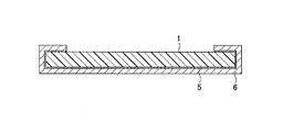
Next, as illustrated in FIG. 1C, an adhesive layer 5 having a thickness of 0.05 mm, for example, is formed on the lower surface of the core 1. An adhesive agent used for the adhesive layer 5 is not limited to a particular adhesive agent as long as the adhesive agent has elasticity after curing, and may be the same as the adhesive agent used for the adhesive layer 2. The thickness of the adhesive layer 5 may be in a range of 0.05 mm to 0.15 mm, for example. A metal layer 6 is adhered to the adhesive layer 5. The metal layer 6 is formed by a metal or alloy that is relatively soft and suited for bending, such as tin (Sn), zinc (Zn), lead (Pb), indium (In), or an alloy including at least one of these metals, and has a thickness of 0.30 mm, for example. In this example, the metal forming the pattern of the metal layer formed on the insulator layer 4 and the metal forming the metal layer 6 are different. The thickness of the metal layer 6 may be in a range of 0.15 mm to 0.30 mm, for example.
Next, as illustrated in FIG. 1D, the adhesive layer 5 and the metal layer 6 are folded at both end parts of the core 1. In the example illustrated in FIG. 1D, the adhesive layer 5 and the metal layer 6 are once bent in a vertical direction (upward direction) along the end parts of the core 1, and are further bent in a horizontal direction (that is, in a direction towards the central part provided with the tag chip 3) along an upper surface of the insulator layer 4. In other words, the adhesive layer 5 and the metal layer 6 are folded in a horizontal U-shape at both end parts of the core 1. Accordingly, both end parts of the adhesive layer 5 are adhered on the upper surface of the insulator layer 4. The RFID tag illustrated in FIG. 1D can be made thin because the thicknesses of the adhesive layers 2 and 5 are slightly reduced (for example, by approximately 10%) during the curing, and the thickness of the RFID tag is 1.745 mm, for example. In addition, a cost and a weight of the RFID tag can also be reduced.
At the folded parts where the metal layer 6 is folded in the horizontal U-shape at both end parts of the core 1, the metal layer 6 and the dipole antenna formed by the pattern of the metal layer on the insulator layer 4 overlap, to form a loop-shaped antenna. Hence, even in a case in which the RFID tag is mounted on a metal surface, for example, it is possible to improve a communication distance communicable between the RFID tag and a tag reader (not illustrated) or a tag writer (not illustrated).
In addition, because the folded parts of the metal layer 6 hold both ends of the insulator layer 4 or the like, even in a case in which the entire RFID tag is bent when mounting the RFID tag on a curved surface, for example, it was confirmed that the insulator layer 4, the metal layer 6, or the like of the RFID tag do not separate from the core 1, and that wrinkles or cracks are uneasily formed in the RFID tag. Moreover, even in a case in which a lower surface of the RFID tag illustrated in FIG. 1D is mounted on a curved surface having a radius of curvature that is 15 mm, for example, using an adhesive tape, it was confirmed that the RFID tag is uneasily broken or damaged. Hence, it was confirmed that the RFID tag is suited for mounting on the curved surface.
Second Embodiment
Next, a description will be given of the manufacturing method of the RFID tag in a second embodiment, by referring to FIGS. 2A through 2D. FIGS. 2A through 2D are cross sectional views for explaining the manufacturing method of the RFID tag in the second embodiment. In FIGS. 2A through 2D, those parts that are the same as those corresponding parts in FIGS. 1A through 1D are designated by the same reference numerals, and a description thereof will be omitted.
First, as illustrated in FIG. 2A, the core 1 formed by an elastic material is prepared.
Next, as illustrated in FIG. 28, the adhesive layer 5 is formed on the lower surface of the core 1. The metal layer 6 is adhered on the adhesive layer 5.
Next, as illustrated in FIG. 2C, the adhesive layer 5 and the metal layer 6 are folded at both end parts of the core 1. In the example illustrated in FIG. 2C, the adhesive layer 5 and the metal layer 6 are once bent in a vertical direction (upward direction) along the end parts of the core 1, and are further bent in a horizontal direction (that is, in a direction towards a central part provided with the tag chip 3) along the upper surface of the core 1. In other words, the adhesive layer 5 and the metal layer 6 are folded in a horizontal U-shape at both end parts of the core 1. Accordingly, both end parts of the adhesive layer 5 are adhered on the upper surface of the core 1.
Next, as illustrated in FIG. 2D, the adhesive layer 2 is formed on the upper surface of the core 1, and on an upper surface of folded parts where the metal layer 6 is folded in the horizontal U-shape at both end parts of the core 1. The tag chip 3 is provided on the surface of the insulator layer 4 formed by an elastic material, and formed with the pattern of the metal layer (not illustrated). The surface (lower surface in FIG. 2D) of the insulator layer 4 provided with the pattern of the metal layer and the tag chip 3 is adhered on the adhesive layer 2, and formed with the pattern of the metal layer (not illustrated). The RFID tag illustrated in FIG. 2D can be made thin because the thicknesses of the adhesive layers 2 and are slightly reduced during the curing, and the thickness of the RFID tag is 1.745 mm, for example. In addition, the cost and the weight of the RFID tag can also be reduced. Moreover, because the insulator layer 4 is formed on the folded parts of the metal layer 6, not only the lower surface but also the upper surface of the RFID tag can be made flat.
At the folded parts where the metal layer 6 is folded in the horizontal U-shape at both end parts of the core 1, the metal layer 6 and the dipole antenna formed by the pattern of the metal layer on the insulator layer 4 overlap, to form a loop-shaped antenna. Hence, even in a case in which the RFID tag is mounted on a metal surface, for example, it is possible to improve the communication distance communicable between the RFID tag and the tag reader (not illustrated) or the tag writer (not illustrated).
In addition, because the folded parts of the metal layer 6 hold both ends of the core 1, the insulator layer 4, or the like, even in a case in which the entire RFID tag is bent when mounting the RFID tag on a curved surface, for example, it was confirmed that the insulator layer 4, the metal layer 6, or the like of the RFID tag do not separate from the core 1, and that wrinkles or cracks are uneasily formed in the RFID tag. Moreover, even in a case in which a lower surface or an upper surface of the RFID tag illustrated in FIG. 2D is mounted on a curved surface having a radius of curvature that is 15 mm, for example, using an adhesive tape, it was confirmed that the RFID tag is uneasily broken or damaged. Hence, it was confirmed that the RFID tag is suited for mounting on the curved surface.
Third Embodiment
Next, a description will be given of the manufacturing method of the RFID tag in a third embodiment, by referring to FIGS. 3A through 3D. FIGS. 3A through 3D are cross sectional views for explaining the manufacturing method of the RFID tag in the third embodiment. In FIGS. 3A through 3D, those parts that are the same as those corresponding parts in FIGS. 1A through 1D are designated by the same reference numerals, and a description thereof will be omitted. In this embodiment, a protection layer is formed on the upper surfaces of the insulator layer 4 and the folded parts in FIG. 1D.
As illustrated in FIGS. 3A and 3B, a protection layer 12 is formed on the upper surface of the RFID tag in the first embodiment illustrated in FIG. 1D, via an adhesive layer 11. An adhesive agent used for the adhesive layer 11 is not limited to a particular adhesive agent as long as the adhesive agent has elasticity after curing, and may be the same as the adhesive agent used for the adhesive layer 2 or the adhesive layer 5. A material used for the protection layer 12 is not limited to a particular material as long as the material has elasticity, and may be a flame resistant material, for example. The adhesive layer 11 has a thickness of 0.05 mm, for example, and the protection layer 12 has a thickness of 0.15 mm, for example. A combination of the adhesive layer 11 and the protection layer 12 may be a film coated with an adhesive agent, for example. The adhesive layer 11 may have a thickness in a range of 0.05 mm to 0.15 mm, for example. In addition, the protection layer 12 may have a thickness in a range of 0.05 mm to 0.15 mm, for example.
Next, as illustrated in FIGS. 3C and 3D, an adhesive layer 13 is formed on a lower surface of the metal layer 6. An adhesive agent used for the adhesive layer 13 is not limited to a particular adhesive agent as long as the adhesive agent has elasticity after curing, and may be the same as the adhesive agent used for the adhesive layer 2, or the adhesive layer 5, or the adhesive layer 11. The adhesive layer 13 has a thickness of 0.05 mm, for example. The adhesive layer 13 may be formed by an adhesive tape, for example. The adhesive layer 13 may have a thickness in a range of 0.05 mm to 0.15 mm, for example. The RFID tag illustrated in FIG. 3D can be made thin because the thicknesses of the adhesive layers 2, 5, 11, and 13 are slightly reduced during the curing, and the thickness of the RFID tag is 1.94 mm, for example. In addition, the cost and the weight of the RFID tag can also be reduced. Moreover, because the protection layer 12 is formed on the folded parts of the metal layer 6, not only the lower surface but also the upper surface of the RFID tag can be made flat. Furthermore, in a case in which the flame resistant material is used for the protection layer 12, the RFID tag can be used in a high-temperature environment, for example.
At the folded parts where the metal layer 6 is folded in the horizontal U-shape at both end parts of the core 1, the metal layer 6 and the dipole antenna formed by the pattern of the metal layer on the insulator layer 4 overlap, to form a loop-shaped antenna. Hence, even in a case in which the RFID tag is mounted on a metal surface, for example, it is possible to improve the communication distance communicable between the RFID tag and the tag reader (not illustrated) or the tag writer (not illustrated).
In addition, because the folded parts of the metal layer 6 hold both ends of the core 1, the insulator layer 4, or the like, even in a case in which the entire RFID tag is bent when mounting the RFID tag on a curved surface, for example, it was confirmed that the insulator layer 4, the metal layer 6, or the like of the RFID tag do not separate from the core 1, and that wrinkles or cracks are uneasily formed in the RFID tag. Moreover, even in a case in which the RFID tag illustrated in FIG. 3D is mounted on a curved surface having a radius of curvature that is 15 mm, for example, using an adhesive tape for the adhesive layer 13, or the protection layer 12 of the RFID tag illustrated in FIG. 3C is mounted on the curved surface having the radius of curvature that is 15 mm, for example, using an adhesive tape, it was confirmed that the RFID tag is uneasily broken or damaged. Hence, it was confirmed that the RFID tag is suited for mounting on the curved surface.
Fourth Embodiment
Next, a description will be given of the manufacturing method of the RFID tag in a fourth embodiment, by referring to FIGS. 4A through 4D. FIGS. 4A through 4D are cross sectional views for explaining the manufacturing method of the RFID tag in the fourth embodiment. In FIGS. 4A through 4D, those parts that are the same as those corresponding parts in FIGS. 1A through 1D are designated by the same reference numerals, and a description thereof will be omitted.
In this embodiment, as illustrated in FIG. 4C, a length of the adhesive layer 5 in the horizontal direction is shorter than a length of the metal layer in the horizontal direction. For this reason, as illustrated in FIG. 4D, when the adhesive layer 5 and the metal layer 6 are folded at both end parts of the core 1, a gap 8 is formed by the core 1, the metal layer 6, and the insulator layer 4 at both the end parts of the core 1. This gap 8 is formed at the end parts of the core 1, between the lower surface of the core 1 and the metal layer 6, between the side surface of the core 1 and the metal layer 6, and between the upper surface of the insulator layer 4 and the metal layer 6. Both end parts of the adhesive layer 5 are adhered on the upper surface of the insulator layer 4. The RFID tag illustrated in FIG. 4D can be made thin because the thicknesses of the adhesive layers 2 and 5 are slightly reduced during the curing, and the thickness of the RFID tag is 1.745 mm, for example. In addition, the cost and the weight of the RFID tag can also be reduced.
At the folded parts where the metal layer 6 is folded in the horizontal U-shape at both end parts of the core 1, the metal layer 6 and the dipole antenna formed by the pattern of the metal layer on the insulator layer 4 overlap, to form a loop-shaped antenna. Hence, even in a case in which the RFID tag is mounted on a metal surface, for example, it is possible to improve the communication distance communicable between the RFID tag and the tag reader (not illustrated) or the tag writer (not illustrated).
In addition, because the folded parts of the metal layer 6 hold both ends of the core 1, the insulator layer 4, or the like, and a part of a distortion of the core 1 when the RFID tag is bent is absorbed by the gap 8, even in a case in which the entire RFID tag is bent when mounting the RFID tag on a curved surface, for example, it was confirmed that the insulator layer 4, the metal layer 6, or the like of the RFID tag do not separate from the core 1, and that wrinkles or cracks are uneasily formed in the RFID tag. Moreover, even in a case in which a lower surface of the RFID tag illustrated in FIG. 4D is mounted on a curved surface having a radius of curvature that is 15 mm, for example, using an adhesive tape, it was confirmed that the RFID tag is uneasily broken or damaged. Hence, it was confirmed that the RFID tag is suited for mounting on the curved surface.
Fifth Embodiment
Next, a description will be given of the manufacturing method of the RFID tag in a fifth embodiment, by referring to FIGS. 5A through 5D. FIGS. 5A through 5D are cross sectional views for explaining the manufacturing method of the RFID tag in the fifth embodiment. In FIGS. 5A through 5D, those parts that are the same as those corresponding parts in FIGS. 2A through 2D are designated by the same reference numerals, and a description thereof will be omitted.
In this embodiment, as illustrated in FIG. 5C, the length of the adhesive layer 5 in the horizontal direction is shorter than the length of the metal layer in the horizontal direction. For this reason, as illustrated in FIG. 5D, when the adhesive layer 5 and the metal layer 6 are folded at both end parts of the core 1, the gap 8 is formed by the core 1, the metal layer 6, and the insulator layer 4 at both the end parts of the core 1. This gap 8 is formed at the end parts of the core 1, between the lower surface of the core 1 and the metal layer 6, between the side surface of the core 1 and the metal layer 6, and between the upper surface of the core 1 and the metal layer 6. Both end parts of the adhesive layer 5 are adhered on the upper surface of the insulator layer 4. The RFID tag illustrated in FIG. 5D can be made thin because the thicknesses of the adhesive layers 2 and 5 are slightly reduced during the curing, and the thickness of the RFID tag is 1.745 mm, for example. In addition, the cost and the weight of the RFID tag can also be reduced.
At the folded parts where the metal layer 6 is folded in the horizontal U-shape at both end parts of the core 1, the metal layer 6 and the dipole antenna formed by the pattern of the metal layer on the insulator layer 4 overlap, to form a loop-shaped antenna. Hence, even in a case in which the RFID tag is mounted on a metal surface, for example, it is possible to improve the communication distance communicable between the RFID tag and the tag reader (not illustrated) or the tag writer (not illustrated).
In addition, because the folded parts of the metal layer 6 hold both ends of the core 1 or the like, and a part of a distortion of the core 1 when the RFID tag is bent is absorbed by the gap 8, even in a case in which the entire RFID tag is bent when mounting the RFID tag on a curved surface, for example, it was confirmed that the insulator layer 4, the metal layer 6, or the like of the RFID tag do not separate from the core 1, and that wrinkles or cracks are uneasily formed in the RFID tag. Moreover, even in a case in which the lower surface of the RFID tag illustrated in FIG. 5D is mounted on a curved surface having a radius of curvature that is 15 mm, for example, using an adhesive tape, it was confirmed that the RFID tag is uneasily broken or damaged. Hence, it was confirmed that the RFID tag is suited for mounting on the curved surface.
Sixth Embodiment
Next, a description will be given of the manufacturing method of the RFID tag in a sixth embodiment, by referring to FIGS. 6A through 6D. FIGS. 6A through 6D are cross sectional views for explaining the manufacturing method of the RFID tag in the sixth embodiment. In FIGS. 6A through 6D, those parts that are the same as those corresponding parts in FIGS. 1A through 1D are designated by the same reference numerals, and a description thereof will be omitted. In this embodiment, parts of the RFID tag other than a mounting surface are covered by a protection member, to protect the RFID tag from a temperature environment, a humidity environment, a vibration environment, shock, or the like.
First, as illustrated in FIG. 6A, a box-shaped protection member 21 is prepared, and as illustrated in FIG. 68B, an adhesive agent 22 is coated on an inner part of the protection member 21. The protection member 21 is formed by an elastomer, such as silicone rubber or the like, having a thickness of 0.40 mm, for example. The protection member 21 may have a thickness in a range of 0.20 mm to 0.40 nm, for example. The adhesive agent 22 is not limited to a particularly adhesive agent as long as the adhesive agent has elasticity after curing, and may be RTV (Room Temperature Vulcanization) silicone rubber or the like, for example.
Next, as illustrated in FIG. 6C, the RFID tag in the first embodiment illustrated in FIG. 1D is turned upside-down, to insert the RFID tag from the side of the insulator layer 4 into an inner side the protection member 21. Accordingly, as illustrated in FIG. 6D in which the RFID tag is further turned upside-down, the folded parts of the insulator layer 4 and the metal layer 6 of the RFID tag are adhered to the protection member 21 by the adhesive agent 22. In FIG. 6D, the lower surface of the protection member 21 and the exposed lower surface of the metal layer 6 of the RFID tag lie approximately on the same plane, and may be mounted on a tag mounting surface, such as a curved surface or the like, using an adhesive tape. The thickness of the RFID tag illustrated in FIG. 6D, including the protection member 21, is 2.145 mm, for example.
At the folded parts where the metal layer 6 is folded in the horizontal U-shape at both end parts of the core 1, the metal layer 6 and the dipole antenna formed by the pattern of the metal layer on the insulator layer 4 overlap, to form a loop-shaped antenna. Hence, even in a case in which the RFID tag is mounted on a metal surface, for example, it is possible to improve the communication distance communicable between the RFID tag and the tag reader (not illustrated) or the tag writer (not illustrated).
In addition, because the folded parts of the metal layer 6 hold both ends of the core 1, the insulator layer 4, or the like, and the folded parts are held by the protection member 21, even in a case in which the entire RFID tag is bent when mounting the RFID tag on a curved surface, for example, it was confirmed that the insulator layer 4, the metal layer 6, or the like of the RFID tag do not separate from the core 1, and that wrinkles or cracks are uneasily formed in the RFID tag. Moreover, even in a case in which the lower surface of the protection member 21 and the exposed lower surface of the metal layer 6 of the RFID tag illustrated in FIG. 6D are mounted on a curved surface having a radius of curvature that is 15 mm, for example, using an adhesive tape, it was confirmed that the RFID tag is uneasily broken or damaged. Hence, it was confirmed that the RFID tag is suited for mounting on the curved surface. Furthermore, it was confirmed that the RFID tag is protected by the protection member 21 from the temperature environment, the humidity environment, the vibration environment, the shock, or the like.
Instead of inserting the RFID tag illustrated in FIG. 1D, the RFID tag illustrated in FIG. 2D may be inserted from the side of the insulator layer 4 into the inner side of the protection member 21, the RFID tag illustrated in FIG. 3D may be inserted from the side of the protection layer 12 into the inner side of the protection member 21, the RFID tag illustrated in FIG. 4D may be inserted from the side of the insulator layer 4 into the inner side of the protection member 21, and the RFID tag illustrated in FIG. 5D may be inserted from the side of the insulator layer 4 into the inner side the protection member 21.
Seventh Embodiment
Next, a description will be given of the manufacturing method of the RFID tag in a seventh embodiment, by referring to FIGS. 7A through 7D. FIGS. 7A through 7D are cross sectional views for explaining the manufacturing method of the RFID tag in the seventh embodiment. In FIGS. 7A through 7D, those parts that are the same as those corresponding parts in FIGS. 1A through 1D are designated by the same reference numerals, and a description thereof will be omitted. In this embodiment, the entire surface of the RFID tag is covered by protection members, and a filler material fills a gap between the RFID tag and the protection members, to protect the RFID tag from the temperature environment, the humidity environment, the vibration environment, the shock, or the like.
First, as illustrated in FIG. 7A, a box-shaped protection member 31 is prepared, and as illustrated in FIG. 7B, an adhesive agent 32 is coated on an inner part of the protection member 31. The protection member 31 is formed by an elastomer, such as silicone rubber or the like, having a thickness of 0.40 mm, for example. The protection member 31 may have a thickness in a range of 0.20 mm to 0.40 mm, for example. The adhesive agent 32 is not limited to a particularly adhesive agent as long as the adhesive agent has elasticity after curing, and may be RTV silicone rubber or the like, for example.
Next, as illustrated in FIGS. 7B and 7C, the RFID tag in the first embodiment illustrated in FIG. 1D is inserted from the side of the metal layer 6 into an inner side the protection member 31. Accordingly, as illustrated in FIG. 7C, the metal layer 6 of the RFID tag is adhered on the protection member 31 by the adhesive agent 32. In addition, as illustrated in FIG. 7C, an adhesive agent 33 is coated on the upper surface of the RFID tag, and a box-shaped protection member 34 is adhered on the RFID tag and the protection member 31 via the adhesive agent 33. The protection member 34 may be made of the same material as the protection member 31, and have the same thickness as the protection member 31. The adhesive agent 33 may be made of the same material as the adhesive agent 32. The protection members 31 and 34 that are mutually adhered form a package or a casing that protects the RFID tag. An adhesive agent 35 at the parts connecting the protection members 31 and 34 may be any of the adhesive agent 32, the adhesive agent 33, a mixture of the adhesive agents 32 and 33, and an adhesive agent other than the adhesive agents 32 and 33. Accordingly, as illustrated in FIG. 7D, the RFID tag is encapsulated by the protection members 31 and 34, and a space between the RFID tag and the protection members 31 and 34 is filled by the adhesive agents 32 and 33 that also function as a filler material. The adhesive agents 32 and 33 that function as the filler material can suppress a change in shape of the RFID tag encapsulated within the protection members 31 and 34, particularly due to a change in pressure. In FIG. 7D, the RFID tag may be mounted on the tag mounting surface, such as a curved surface or the like, by mounting a lower surface of the protection member 31 on the tag mounting surface using an adhesive tape. The thickness of the RFID tag, including the protection members 31 and 34 illustrated in FIG. 7D, is 2.590 mm, for example.
At the folded parts where the metal layer 6 is folded in the horizontal U-shape at both end parts of the core 1, the metal layer 6 and the dipole antenna formed by the pattern of the metal layer on the insulator layer 4 overlap, to form a loop-shaped antenna. Hence, even in a case in which the RFID tag is mounted on a metal surface, for example, it is possible to improve the communication distance communicable between the RFID tag and the tag reader (not illustrated) or the tag writer (not illustrated).
In addition, because the folded parts of the metal layer 6 hold both ends of the core 1, the insulator layer 4, or the like, and the folded parts are held by the protection members 31 and 34, even in a case in which the entire RFID tag is bent when mounting the RFID tag on a curved surface, for example, it was confirmed that the insulator layer 4, the metal layer 6, or the like of the RFID tag do not separate from the core 1, and that wrinkles or cracks are uneasily formed in the RFID tag. Moreover, even in a case in which the lower surface of the protection member 21 of the RFID tag illustrated in FIG. 7D is mounted on a curved surface having a radius of curvature that is 15 mm, for example, using an adhesive tape, it was confirmed that the RFID tag is uneasily broken or damaged. Hence, it was confirmed that the RFID tag is suited for mounting on the curved surface. Furthermore, it was confirmed that the RFID tag is protected by the protection members 31 and 34 from the temperature environment, the humidity environment, the vibration environment, the shock, or the like.
Instead of inserting the RFID tag illustrated in FIG. 1D, the RFID tag illustrated in FIG. 2D may be inserted from the side of the metal layer 6 into the inner side of the protection member 31, and the RFID tag illustrated in FIG. 3D may be inserted from the side of the metal layer 6 into the inner side of the protection member 31. In addition, the RFID tag illustrated in FIG. 1D may be inserted from the side of the insulator layer 4 into the inner side of the protection member 31. Similarly, instead of inserting the RFID tag illustrated in FIG. 1D, the RFID tag illustrated in FIG. 2D may be inserted from the side of the insulator layer 4 into the inner side of the protection member 31, and the RFID tag illustrated in FIG. 3D may be inserted from the side of the protection layer 12 into the inner side of the protection member 31.
In addition, the RFID tag may first be inserted into the protection member 34, and the protection member 31 may thereafter be connected to the protection member 34. Moreover, instead inserting the RFID tag illustrated in FIG. 1D, the RFID tag illustrated in FIG. 2D or illustrated in FIG. 3D may be inserted in a similar manner.
Furthermore, although depths of the inner parts of the protection members 31 and 34 are approximately the same in the example illustrated in FIGS. 7A through 7D, the depth of one of the protection members 31 and 34 may of course be deeper than the other.
Eighth Embodiment
Next, a description will be given of the manufacturing method of the RFID tag in an eighth embodiment, by referring to FIGS. 8A through 8D. FIGS. 8A through 8D are cross sectional views for explaining the manufacturing method of the RFID tag in the eighth embodiment. In FIGS. 8A through 8D, those parts that are the same as those corresponding parts in FIGS. 7A through 7D are designated by the same reference numerals, and a description thereof will be omitted. In this embodiment, the entire surface of the RFID tag is covered by protection members, and a gap is maintained between the RFID tag and the protection members, to protect the RFID tag from the temperature environment, the humidity environment, the vibration environment, the shock, or the like.
First, as illustrated in FIG. 8A, the box-shaped protection member 31 is prepared.
Next, as illustrated in FIG. 8B, the RFID tag in the fourth embodiment illustrated in FIG. 4D is inserted from the side of the metal layer 6 into the inner part of the protection member 31, as illustrated in FIG. 8C. In addition, as illustrated in FIG. 8C, the RFID tag and the protection member 31 are covered by the box-shaped protection member 34, and the protection members 31 and 34 are adhered by the adhesive agent 35. As a result, as illustrated in FIG. 8D, the RFID tag is encapsulated by the protection members 31 and 34, and the space between the RFID tag and the protection members 31 and 34 is maintained. In FIG. 8D, the RFID tag may be mounted on the tag mounting surface, such as a curved surface or the like, by mounting the lower surface of the protection member 31 using an adhesive tape. The thickness of the RFID tag, including the protection members 31 and 34 illustrated in FIG. 8D, is 2.590 mm, for example.
At the folded parts where the metal layer 6 is folded in the horizontal U-shape at both end parts of the core 1, the metal layer 6 and the dipole antenna formed by the pattern of the metal layer on the insulator layer 4 overlap, to form a loop-shaped antenna. Hence, even in a case in which the RFID tag is mounted on a metal surface, for example, it is possible to improve the communication distance communicable between the RFID tag and the tag reader (not illustrated) or the tag writer (not illustrated).
In addition, because the folded parts of the metal layer 6 hold both ends of the core 1, the insulator layer 4, or the like, and a part of the distortion of the core 1 when the RFID tag is bent is absorbed by the gap 8 and the gap between the RFID tag and the protection members 31 and 34, even in a case in which the entire RFID tag is bent when mounting the RFID tag on a curved surface, for example, it was confirmed that the insulator layer 4, the metal layer 6, or the like of the RFID tag do not separate from the core 1, and that wrinkles or cracks are uneasily formed in the RFID tag. Moreover, even in a case in which the entire RFID tag is bent when mounting the RFID tag on a curved surface, for example, it was confirmed that the insulator layer 4, the metal layer 6, or the like of the RFID tag do not separate from the core 1, and that wrinkles or cracks are uneasily formed in the RFID tag. Furthermore, even in a case in which the lower surface of the protection member 31 of the RFID tag illustrated in FIG. 8D is mounted on a curved surface having a radius of curvature that is 15 mm, for example, using an adhesive tape, it was confirmed that the RFID tag is uneasily broken or damaged. Hence, it was confirmed that the RFID tag is suited for mounting on the curved surface. In addition, it was confirmed that the RFID tag is protected by the protection members 31 and 34 from the temperature environment, the humidity environment, the vibration environment, the shock, or the like. In the case of this embodiment, it is possible to reduce the weight of the RFID tag including the protection members 31 and 34 when compared to the seventh embodiment described above, because this embodiment does not use a filler material to fill the gap.
Instead of inserting the RFID tag illustrated in FIG. 4D, the RFID tag illustrated in FIG. 5D may be inserted from the side of the metal layer 6 into the inner side of the protection member 31. In addition, the RFID tag illustrated in FIG. 4D may be inserted from the side of the insulator layer 4 into the inner side of the protection member 31. Similarly, instead of inserting the RFID tag illustrated in FIG. 4D, the RFID tag illustrated in FIG. 5D may be inserted from the side of the insulator layer 4 into the inner side of the protection member 31.
In addition, the RFID tag may first be inserted into the protection member 34, and the protection member 31 may thereafter be connected to the protection member 34. Moreover, instead inserting the RFID tag illustrated in FIG. 4D, the RFID tag illustrated in FIG. 5D may be inserted in a similar manner.
Furthermore, although depths of the inner parts of the protection members 31 and 34 are approximately the same in the example illustrated in FIGS. 8A through 8D, the depth of one of the protection members 31 and 34 may of course be deeper than the other. In a case in which the RFID tag does not need to be completely encapsulated by the protection members 31 and 34, the adhesive agent 35 may be intermittently coated, to form an opening communicating a space surrounded by the protection members 31 and 34 to an outside of the protection members 31 and 34.
FIG. 9 is a plan view, partially in a perspective, of the RFID tag in the eighth embodiment. For the sake of convenience, FIG. 9 illustrates the RFID tag in a state in which the protection members 31 and 34 are removed. As illustrated in FIG. 9, a pattern 41 of a metal layer is formed on a surface (lower side of paper in FIG. 9) of the insulator layer 4 on the side of the core 1. The shape of the pattern 41 of the metal layer is not limited to a particular shape as long as the pattern 41 is able to form a dipole antenna. Terminals of the tag chip 3 that is indicated by a solid line for the sake of convenience to facilitate visual confirmation are electrically connected to the pattern 41 of the metal layer. The metal layer 6 and a part of the pattern 41 of the metal layer on the insulator layer 4 overlap at the folded parts of the metal layer 6.
The pattern of the metal layer formed on the insulator layer 4 in the first through eighth embodiments described above may be similar to the pattern 41 of the metal layer illustrated in FIG. 9.
Ninth Embodiment
FIG. 10 is a cross sectional view for explaining the manufacturing method of the RFID tag in a ninth embodiment. In FIG. 10, those parts that are the same as those corresponding parts in FIGS. 1A through 1D are designated by the same reference numerals, and a description thereof will be omitted. In this embodiment, the insulator layer 4 is folded at both end parts of the core 1. In this example, the insulator layer 4 is once bent in a vertical direction (downward direction) along the end parts of the core 1, and is further bent in a horizontal direction (that is, in a direction towards the central part of the core 1) along the lower surface of the metal layer 6. In other words, the insulator layer 4 is folded in a horizontal U-shape at both end parts of the core 1. The adhesive layer 2 and the insulator layer 4 may have approximately the same sizes, so that the insulator layer 4 is adhered to the side surface of the core 1 and the lower surface of the metal layer 6 via the adhesive layer 2. The RFID tag illustrated in FIG. 10 can be made thin because the thicknesses of the adhesive layers 2 and 5 are slightly reduced during the curing, and the thickness of the RFID tag is 1.505 mm, for example. In addition, the cost and the weight of the RFID tag can also be reduced.
At the folded parts where the insulator layer 4 is folded in the horizontal U-shape at both end parts of the core 1, the metal layer 6 and the dipole antenna formed by the pattern of the metal layer on the insulator layer 4 overlap, to form a loop-shaped antenna. Hence, even in a case in which the RFID tag is mounted on a metal surface, for example, it is possible to improve the communication distance communicable between the RFID tag and the tag reader (not illustrated) or the tag writer (not illustrated).
In addition, in order to provide the gap 8 such as that illustrated in FIGS. 5C and 5D at the folded parts of the insulator layer 4, it is possible not to form the adhesive layers 2 and 5 on the entire upper surface and lower surface of the core 1, or on the side surfaces of the core 1. In this case, because the insulator layer 4 holds both ends of the core 1 or the like, and a part of a distortion of the core 1 when the RFID tag is bent is absorbed by the gap 8, even in a case in which the entire RFID tag is bent when mounting the RFID tag on a curved surface, for example, it was confirmed that the insulator layer 4, the metal layer 6, or the like of the RFID tag do not separate from the core 1, and that wrinkles or cracks are uneasily formed in the RFID tag. Moreover, even in a case in which the lower surface of the RFID tag illustrated in FIG. 10 is mounted on a curved surface having a radius of curvature that is 15 mm, for example, using an adhesive tape, it was confirmed that the RFID tag is uneasily broken or damaged. Hence, it was confirmed that the RFID tag is suited for mounting on the curved surface.
The protection layer 12 may be formed on the lower surface of the RFID tag illustrated in FIG. 10 via the adhesive layer 11 similar to that of FIGS. 3A through 3D.
Tenth Embodiment
FIG. 11 is a cross sectional view for explaining the manufacturing method of the RFID tag in a tenth embodiment. In FIG. 11, those parts that are the same as those corresponding parts in FIGS. 6A through 6D, and FIG. 10 are designated by the same reference numerals, and a description thereof will be omitted. In this embodiment, an RFID tag having a configuration similar to that of FIG. 10 has the protection member 21 adhered thereon by the adhesive agent 22. In addition, an adhesive layer 37 is adhered on the folded parts of the insulator layer 4 and the exposed lower surface of the metal layer 6. The thickness of the RFID tag including the protection member 21 illustrated in FIG. 11 is 1.895 mm, for example.
At the folded parts where the insulator layer 4 is folded in the horizontal U-shape at both end parts of the core 1, the metal layer 6 and the dipole antenna formed by the pattern of the metal layer on the insulator layer 4 overlap, to form a loop-shaped antenna. Hence, even in a case in which the RFID tag is mounted on a metal surface, for example, it is possible to improve the communication distance communicable between the RFID tag and the tag reader (not illustrated) or the tag writer (not illustrated).
In addition, because the folded parts of the insulator layer 4 hold both ends of the core 1, the insulator layer 4, or the like, and the folded parts are held by the protection member 21, even in a case in which the entire RFID tag is bent when mounting the RFID tag on a curved surface, for example, it was confirmed that the insulator layer 4, the metal layer 6, or the like of the RFID tag do not separate from the core 1, and that wrinkles or cracks are uneasily formed in the RFID tag. Moreover, even in a case in which the lower surface of the protection member 21 and the exposed lower surface of the metal layer 6 of the RFID tag illustrated in FIG. 11 are mounted on a curved surface having a radius of curvature that is 15 mm, for example, using an adhesive tape, it was confirmed that the RFID tag is uneasily broken or damaged. Hence, it was confirmed that the RFID tag is suited for mounting on the curved surface. Furthermore, it was confirmed that the RFID tag is protected by the protection member 21 from the temperature environment, the humidity environment, the vibration environment, the shock, or the like.
Eleventh Embodiment
FIG. 12 is a cross sectional view for explaining the manufacturing method of the RFID tag in an eleventh embodiment. In FIG. 12, those parts that are the same as those corresponding parts in FIGS. 1A through 1D are designated by the same reference numerals, and a description thereof will be omitted. In this embodiment, the insulator layer 4 is folded at both end parts of the core 1. In this example, the insulator layer 4 is once bent in a vertical direction (downward direction) along the end parts of the core 1, and is further bent in a horizontal direction (that is, in a direction towards the central part of the core 1) along the lower surface of the core 1. In other words, the insulator layer 4 is folded in a horizontal U-shape at both end parts of the core 1. The adhesive layer 2 and the insulator layer 4 may have approximately the same sizes, so that the insulator layer 4 is adhered to the side surface of the core 1 and a part of the lower surface of the core 1 via the adhesive layer 2. The metal layer 6 is adhered on the folded parts of the insulator layer 4 and the exposed lower surface of the core 1 via the adhesive layer 5. The adhesive layer 5 may also be provided between the metal layer 6 and the folded parts of the insulator layer 4. The RFID tag illustrated in FIG. 12 can be made thin because the thicknesses of the adhesive layers 2 and 5 are slightly reduced during the curing, and the thickness of the RFID tag is 1.505 mm, for example. In addition, the cost and the weight of the RFID tag can also be reduced.
At the folded parts where the insulator layer 4 is folded in the horizontal U-shape at both end parts of the core 1, the metal layer 6 and the dipole antenna formed by the pattern of the metal layer on the insulator layer 4 overlap, to form a loop-shaped antenna. Hence, even in a case in which the RFID tag is mounted on a metal surface, for example, it is possible to improve the communication distance communicable between the RFID tag and the tag reader (not illustrated) or the tag writer (not illustrated).
In addition, because the folded parts of the insulator layer 4 are held by the metal layer 6, even in a case in which the entire RFID tag is bent when mounting the RFID tag on a curved surface, for example, it was confirmed that the insulator layer 4, the metal layer 6, or the like of the RFID tag do not separate from the core 1, and that wrinkles or cracks are uneasily formed in the RFID tag. Moreover, even in a case in which the lower surface of the RFID tag illustrated in FIG. 12 is mounted on a curved surface having a radius of curvature that is 15 mm, for example, using an adhesive tape, it was confirmed that the RFID tag is uneasily broken or damaged. Hence, it was confirmed that the RFID tag is suited for mounting on the curved surface.
The RFID tag illustrated in FIG. 12 may be inserted into the protection member 21 illustrated in FIG. 11.
Twelfth Embodiment
FIG. 13 is a cross sectional view for explaining the manufacturing method of the RFID tag in a twelfth embodiment. In FIG. 13, those parts that are the same as those corresponding parts in FIGS. 7A through 7D, and FIG. 10 are designated by the same reference numerals, and a description thereof will be omitted. In this embodiment, an RFID tag having a configuration similar to that of FIG. 10 is encapsulated by the protection members 31 and 34, and the gap between the RFID tag and the protection members 31 and 34 is filled by the adhesive agents 32 and 33 that also function as the filler material. The adhesive agents 32 and 33 that function as the filler material can suppress a change in shape of the RFID tag encapsulated within the protection members 31 and 34, particularly due to a change in pressure. The thickness of the RFID tag, including the protection members 31 and 34 illustrated in FIG. 13, is 2.35 mm, for example.
At the folded parts where the insulator layer 4 is folded in the horizontal U-shape at both end parts of the core 1, the metal layer 6 and the dipole antenna formed by the pattern of the metal layer on the insulator layer 4 overlap, to form a loop-shaped antenna. Hence, even in a case in which the RFID tag is mounted on a metal surface, for example, it is possible to improve the communication distance communicable between the RFID tag and the tag reader (not illustrated) or the tag writer (not illustrated).
In addition, because the folded parts of the insulator layer 4 hold both ends of the core 1, the metal layer 6, or the like, and the folded parts are held by the protection members 31 and 34, even in a case in which the entire RFID tag is bent when mounting the RFID tag on a curved surface, for example, it was confirmed that the insulator layer 4, the metal layer 6, or the like of the RFID tag do not separate from the core 1, and that wrinkles or cracks are uneasily formed in the RFID tag. Moreover, even in a case in which the lower surface of the protection member 21 of the RFID tag illustrated in FIG. 13 is mounted on a curved surface having a radius of curvature that is 15 mm, for example, using an adhesive tape, it was confirmed that the RFID tag is uneasily broken or damaged. Hence, it was confirmed that the RFID tag is suited for mounting on the curved surface. Furthermore, it was confirmed that the RFID tag is protected by the protection members 31 and 34 from the temperature environment, the humidity environment, the vibration environment, the shock, or the like.
Instead of inserting the RFID tag illustrated in FIG. 10, the RFID tag illustrated in FIG. 12 may be inserted from the side of the metal layer 6 into the inner side of the protection member 31. In addition, the RFID tag illustrated in FIG. 12 may be inserted from the side of the insulator layer 4 into the inner side of the protection member 31.
In addition, the RFID tag may first be inserted into the protection member 34, and the protection member 31 may thereafter be connected to the protection member 34. Moreover, instead inserting the RFID tag illustrated in FIG. 10, the RFID tag illustrated in FIG. 12 may be inserted in a similar manner.
Furthermore, although depths of the inner parts of the protection members 31 and 34 are approximately the same in the example illustrated in FIG. 13, the depth of one of the protection members 31 and 34 may of course be deeper than the other.
It is possible not to fill the space between the RFID tag and the protection members 31 and 34 by the filler material.
FIG. 14 is a plan view, partially in a perspective, of the RFID tag in the twelfth embodiment. For the sake of convenience, FIG. 14 illustrates the RFID tag in a state in which the protection members 31 and 34 are removed. As illustrated in FIG. 14, the pattern 41 of the metal layer is formed on the surface (lower side of paper in FIG. 14) of the insulator layer 4 on the side of the core 1. The shape of the pattern 41 of the metal layer is not limited to a particular shape as long as the pattern 41 is able to form a dipole antenna. Terminals of the tag chip 3 that is indicated by a solid line for the sake of convenience to facilitate visual confirmation are electrically connected to the pattern 41 of the metal layer.
The pattern of the metal layer formed on the insulator layer 4 in the ninth through eleventh embodiments described above may be similar to the pattern 41 of the metal layer illustrated in FIG. 14.
In each of the embodiments described above, it was confirmed that, by appropriately selecting the thicknesses of each of the layers, the thickness of the RFID tag using no protection member 21 or no protection members 31 and 34 can be reduced to approximately 1.0 mm. The RFID tag using no protection member 21 or no protection members 31 and 34 may be used in an interior environment (environment in which the temperature, the pressure, or the like are adjusted, as in the case of a cabin of an aircraft) of RTCA/DO-160, SAE/AS5678, or the like, for example, which are standards for the RFID tag. In addition, it was confirmed that the thickness of the RFID tag using the protection member 21 or the protection members 31 and 34 can be reduced to approximately 2.0 mm. The RFID tag using the protection member 21 or the protection members 31 and 34 may be used in an exterior environment (environment in which the temperature, the pressure, or the like are not adjusted, as in the case of a landing gear well of the aircraft) of RTCA/DO-160, SAE/AS5678, or the like, for example, which are standards for the RFID tag, and a power plant environment (high-temperature environment, such as a periphery of an engine of the aircraft).
Next, a description will be given of the configuration of the passive type RFID tag, by referring to FIG. 15. FIG. 15 is a block diagram illustrating an example of a hardware configuration of the passive type RFID tag. The passive type RFID tag illustrated in FIG. 15 includes a loop-shaped antenna 51 which is an example of the dipole antenna, and a tag chip 52-1 which is an example of the semiconductor chip. The tag chip 52-1 include a power generating part 53 which is an example of a power supply, a transmitting and receiving part 54 which is an example of a communication part, a data processing part 55, and a memory 56 which is an example of a storage part. The power generating part 53 generates, by a known method, a power supply voltage from radio waves received via the antenna 51, and supplies the power supply voltage to each part within the tag chip 52-1. For example, the transmitting and receiving part 54 may include a demodulator part that demodulates received data according to a modulation technique corresponding to a modulation technique of the tag writer (not illustrated), and a modulator that modules transmitting data according to a modulation technique corresponding to a modulation technique of the tag reader (not illustrated). The data processing part 55 performs a decoding process to subject the demodulated received data to a decoding corresponding to a coding technique of the tag writer, a coding process to subject the transmitting data to be modulated to a coding corresponding to a coding technique of the tag reader, a control process to control read and write of the data with respect to the memory 56, or the like. The data processing part 55 may include a codec that performs the decoding process and the coding process, and a controller that performs the control process. In addition, the data processing part 55 may include a processor, such as a CPU (Central Processing Unit), that performs the decoding process, the coding process, and the control process. The tag chip 52-1 is mounted at a central part of the surface of the core 1 provided with the metal layer or the dipole antenna, for example, using an adhesive agent or the like.
In the example illustrated in FIG. 15, the tag chip 52-1 may include one or a plurality of sensors 57. In a case in which the tag chip 52-1 includes the sensor 57, data related to information such as the temperature, the humidity, the pressure, or the like detected by the sensor 57 may be stored in the memory 56 together with time information such as the time, the date and time, or the like managed by the data processing part 55.
Next, a description will be given of the configuration of the active type RFID tag having a built-in battery, by referring to FIG. 16. FIG. 16 is a block diagram illustrating an example of a hardware configuration of the active type RFID tag. In FIG. 16, those parts that are the same as those corresponding parts in FIG. 15 are designated by the same reference numerals, and a description thereof will be omitted. The active type RFID tag illustrated in FIG. 16 includes the loop-shaped antenna 51, a tag chip 52-2, and a battery 531 which is an example of a power supply. The battery 531 supplies a power supply voltage to each part within the tag chip 52-2. The type of the battery 531 is not limited to a particular type, and the number of batteries 531 is not limited to a particular number. The tag chip 52-2 and the battery 531 are mounted at the central part of the surface of the core 1 provided with the metal layer or the dipole antenna, for example, using an adhesive agent or the like.
The RFID tag illustrated in FIG. 16 includes functions of the active type RFID tag, however, this RFID tag may form a semi-active type RFID tag that starts communication with a host system, for example, by a system similar to that of the passive type RFID tag.
The active type RFID tag and the semi-active type RFID tag is provided with the battery 531 in place of the power generating part 53, and differ from the passive type RFID tag in that this battery 531 is connected to the chip 52-2. However, the configuration of other parts of the active type RFID tag and the semi-active type RFID tag may be similar to that of the passive type RFID tag. Accordingly, in the first through twelfth embodiments described above in conjunction with FIGS. 1A through 14, the RFID tag may of course form the active type RFID tag or the semi-active type RFID tag by providing the battery 531 in place of the power generating part 53 and connecting this battery 531 to the tag chip 52-1 which corresponds to the tag chip 3.
The disclosed RFID tag is particularly suited for mounting on the curved surface, however, the surface on which the RFID tag is mounted is not limited to the curved surface, and the RFID tag may of course be mounted on a flat surface.
In addition, the shape of the RFID tag in the plan view is not limited to the rectangular shape, and the shape of the RFID tag may be selected arbitrarily according to the usage of the RFID tag.
Further, the RFID tag may be provided integrally On a rewritable RFID sheet, for example. In this case, because the RFID tag in the first through twelfth embodiments can be made thin, the RFID tag may be printed by a known RFID tag so that data related to log information, management information, or the like of the components, for example, are written into the memory of the RFID tag in a manner readable by the RFID tag reader, and character data related to the log information, the management information, or the like of the components are printed on the rewritable RFID sheet in a manner visible by a user.
In each of the embodiments described above, the metal layer and the dipole antenna overlap at the folded parts where one of the metal layer and the dipole antenna is folded at a pair of end parts, however, the overlapping parts of the metal layer and the dipole antenna may be adhered by an adhesive agent. In this case, the adhesive agent adhering the overlapping parts of the metal layer and the dipole antenna may be conductive or non-conductive.
According to the disclosed RFID tag and manufacturing method thereof, it is possible to provide an RFID tag having a loop-shaped antenna and suited for mounting on a curved surface.
Although the embodiments are numbered with, for example, “first,” “second,” . . . or “twelfth,” the ordinal numbers do not imply priorities of the embodiments. Many other variations and modifications will be apparent to those skilled in the art.
All examples and conditional language recited herein are intended for pedagogical purposes to aid the reader in understanding the invention and the concepts contributed by the inventor to furthering the art, and are to be construed as being without limitation to such specifically recited examples and conditions, nor does the organization of such examples in the specification relate to a showing of the superiority and inferiority of the invention. Although the embodiments of the present invention have been described in detail, it should be understood that the various changes, substitutions, and alterations could be made hereto without departing from the spirit and scope of the invention.

Claims (24)

What is claimed is:
1. An RFID tag comprising:
a core formed by a first elastic material and having a first surface, a second surface on an opposite side of the first surface, and a pair of end parts provided on mutually opposite sides and connecting to the first surface and the second surface;
a first metal layer provided on the first surface;
a semiconductor chip provided on the second surface and having a communication part;
an insulator layer provided on the second surface and covering the semiconductor chip, the insulator layer having a third surface opposing the second surface and a fourth surface on an opposite side from the third surface; and
a dipole antenna provided between the second surface and the third surface, the dipole antenna being electrically connected to the semiconductor chip, the dipole antenna includes folded parts that are folded with respect to the core at the pair of end parts, and the folded parts of the dipole antenna overlap the first metal layer.
2. The RFID tag as claimed in claim 1, wherein the first metal layer is made of tin, zinc, lead, indium, or an alloy including at least one of these metals.
3. The RFID tag as claimed in claim 1, wherein the folded parts of the dipole antenna are adhered to the first metal layer.
4. The RFID tag as claimed in claim 1, wherein the dipole antenna is formed by a second metal layer made of a metal different from the first metal layer.
5. The RFID tag as claimed in claim 4, wherein the second metal layer is made of copper, silver, gold, or aluminum.
6. The RFID tag as claimed in claim 4,
wherein the insulator layer has a pattern of the second metal layer formed on the third surface, and
wherein the semiconductor chip is provided on the third surface and is electrically connected to the pattern of the second metal layer.
7. The RFID tag as claimed in claim 6, wherein the insulator layer includes folded parts that are folded with respect to the core at the pair of end parts, and the folded parts of the insulator overlap the first metal layer.
8. The RFID tag as claimed in claim 7, wherein the first metal layer at the pair of end parts is interposed between the first surface and the folded parts of the insulator layer and the dipole antenna.
9. The RFID tag as claimed in claim 7, wherein the folded parts of the insulator layer and the dipole antenna are interposed between the first surface and the first metal layer at the pair of end parts.
10. The RFID tag as claimed in claim 6, further comprising:
a protection member covering the folded parts of the dipole antenna, the insulator layer, and the first metal layer.
11. The RFID tag as claimed in claim 10, further comprising:
a filler material formed by a second elastic material and filling a space surrounded by the protection member.
12. The RFID tag as claimed in claim 10, wherein the protection member encapsulates the core, the first metal layer, the semiconductor chip, the insulator layer, and the dipole antenna.
13. The RFID tag as claimed in claim 6, further comprising:
an adhesive layer provided between the second layer and the third layer,
wherein the semiconductor chip is embedded in the adhesive layer.
14. The RFID tag as claimed in claim 1, wherein the first elastic material is a dielectric.
15. A manufacturing method of an RFID tag, comprising:
forming the RFID tag comprising a metal layer provided on a first surface of a core, a semiconductor chip provided on a second surface of the core on an opposite side from the first surface, an insulator layer provided on the second surface and covering the semiconductor chip, the insulator layer having a third surface opposing the second surface and a fourth surface on an opposite side from the third surface, and a dipole antenna provided between the second surface and the third surface, the dipole antenna being electrically connected to the semiconductor chip, the dipole antenna is folded at folded parts at a pair of end parts of the core, and the dipole antenna at the folded parts overlaps the metal layer;
inserting the RFID tag into a first protection member; and
adhering a second protection member on the first protection member, to encapsulate the RFID tag in a space formed within the first and second protection members.
16. The manufacturing method of the RFID tag as claimed in claim 15, further comprising:
filling a filler material in a gap between the RFID tag and the first and second protection members.
17. The manufacturing method of the RFID tag as claimed in claim 15, wherein:
the core is formed by an elastic material;
the metal layer is formed by tin, zinc, lead, indium, or an alloy including at least one of these metals; and
the dipole antenna is formed by a metal pattern formed on an insulator layer and made of copper, silver, gold, or aluminum.
18. An RFID tag comprising:
a core formed by a first elastic material and having a first surface, a second surface on an opposite side of the first surface, and a pair of end parts provided on mutually opposite sides and connecting to the first surface and the second surface;
a first metal layer provided on the first surface;
a semiconductor chip provided on the second surface and having a communication part;
an insulator layer provided on the second surface and covering the semiconductor chip, the insulator layer having a third surface opposing the second surface and a fourth surface on an opposite side from the third surface; and
a dipole antenna provided between the second surface and the third surface, the dipole antenna being electrically connected to the semiconductor chip,
the insulator layer and the dipole antenna include folded parts that are folded with respect to the core at the pair of end parts, and the folded parts of the insulator layer and the dipole antenna overlap the first metal layer.
19. An RFID tag comprising:
a core formed by a first elastic material and having a first surface, a second surface on an opposite side of the first surface, and a pair of end parts provided on mutually opposite sides and connecting to the first surface and the second surface;
a first metal layer provided on the first surface;
a semiconductor chip provided on the second surface and having a communication part;
an insulator layer provided on the second surface and covering the semiconductor chip, the insulator layer having a third surface opposing the second surface and a flat and continuous fourth surface on an opposite side from the third surface; and
a dipole antenna provided between the second surface and the third surface, the dipole antenna being electrically connected to the semiconductor chip,
the first metal layer includes folded parts that are folded with respect to the core at the pair of end parts, and the folded parts of the first metal layer overlap the dipole antenna.
20. The RFID tag as claimed in claim 19, wherein the folded parts of the first metal layer are provided on the fourth surface of the insulator layer or interposed between the second surface of the core and the third surface of the insulator layer.
21. The RFID tag as claimed in claim 20, further comprising:
a protection member covering the folded parts of the first metal layer, and at least one of the insulator layer and the first metal layer.
22. The RFID tag as claimed in claim 21, wherein the protection member is made of elastomer.
23. The RFID tag as claimed in claim 20, wherein the insulator layer and the dipole antenna at the pair of end parts are interposed between the second surface and the folded parts of the first metal layer.
24. The RFID tag as claimed in claim 20, wherein the folded parts of the first metal layer are interposed between the second surface and each of the insulator layer and the dipole antenna at the pair of end parts.
US15/012,967 2013-08-15 2016-02-02 RFID tag and manufacturing method thereof Expired - Fee Related US9740976B2 (en)

Applications Claiming Priority (1)

Application Number Priority Date Filing Date Title
PCT/JP2013/071973 WO2015022747A1 (en) 2013-08-15 2013-08-15 Rfid tag and method for manufacturing same

Related Parent Applications (1)

Application Number Title Priority Date Filing Date
PCT/JP2013/071973 Continuation WO2015022747A1 (en) 2013-08-15 2013-08-15 Rfid tag and method for manufacturing same

Publications (2)

Publication Number Publication Date
US20160155041A1 US20160155041A1 (en) 2016-06-02
US9740976B2 true US9740976B2 (en) 2017-08-22

Family

ID=52468147

Family Applications (1)

Application Number Title Priority Date Filing Date
US15/012,967 Expired - Fee Related US9740976B2 (en) 2013-08-15 2016-02-02 RFID tag and manufacturing method thereof

Country Status (6)

Country Link
US (1) US9740976B2 (en)
EP (1) EP3035248A4 (en)
JP (1) JP6056978B2 (en)
CN (1) CN105453113A (en)
TW (1) TWI534713B (en)
WO (1) WO2015022747A1 (en)

Cited By (3)

* Cited by examiner, † Cited by third party
Publication number Priority date Publication date Assignee Title
US11580348B2 (en) * 2016-12-14 2023-02-14 Trackonomy Systems, Inc. Transient infrastructure for ubiquitous network communications applications
US11776380B2 (en) 2021-02-19 2023-10-03 Trackonomy Systems, Inc. Client device interactions and asset monitoring at checkpoint locations in an IOT device network
US11836563B2 (en) 2016-12-14 2023-12-05 Trackonomy Systems, Inc. Programmable network node roles in hierarchical communications network

Families Citing this family (7)

* Cited by examiner, † Cited by third party
Publication number Priority date Publication date Assignee Title
US11928537B2 (en) 2013-01-18 2024-03-12 Amatech Group Limited Manufacturing metal inlays for dual interface metal cards
US11341389B2 (en) * 2013-01-18 2022-05-24 Amatech Group Limited Manufacturing metal inlays for dual interface metal cards
JP6056978B2 (en) * 2013-08-15 2017-01-11 富士通株式会社 RFID tag and manufacturing method thereof
GB2542361B (en) * 2015-09-16 2021-03-03 Spa Track Medical Ltd Method of manufacturing an RFID tag assembly and RFID tag assembly
WO2018045550A1 (en) * 2016-09-09 2018-03-15 Hong Kong R&D Centre for Logistics and Supply Chain Management Enabling Technologies Limited A radio frequency communication device and a method for using thereof
JP6798328B2 (en) * 2017-01-25 2020-12-09 Tdk株式会社 Communication device
CN112884110A (en) * 2021-02-03 2021-06-01 上海坤锐电子科技有限公司 Label inlay and electronic label

Citations (47)

* Cited by examiner, † Cited by third party
Publication number Priority date Publication date Assignee Title
US4774521A (en) * 1985-09-30 1988-09-27 Minnesota Mining And Manufacturing Company Resonant marker for use with radio frequency electronic article surveillance system
US6169925B1 (en) * 1999-04-30 2001-01-02 Medtronic, Inc. Telemetry system for implantable medical devices
US20020031997A1 (en) * 1998-05-19 2002-03-14 Lawler Casimir E. Machine readable tag
US20030033713A1 (en) * 2001-08-15 2003-02-20 Hausladen Michael C. RFID tag having integral electrical bridge and method of assembling the same
US6650301B1 (en) * 2002-06-19 2003-11-18 Andrew Corp. Single piece twin folded dipole antenna
US20040074974A1 (en) * 2000-07-19 2004-04-22 Fujio Senba Rfid tag housing structure, rfid tag installation structure and rfid tag communication method
US20040145450A1 (en) * 2003-01-29 2004-07-29 Kabushiki Kaisha Tokai Rika Denki Seisakusho Remote control key for preventing theft of transponder and method for manufacturing the same
US20040169086A1 (en) * 2001-06-07 2004-09-02 Eiji Ohta Ic card
US20040174257A1 (en) * 2003-03-01 2004-09-09 Kuhns David W. Forming electromagnetic communication circuit components using densified metal powder
US6836215B1 (en) * 2002-01-22 2004-12-28 The Standard Register Company Printable identification band with top strip for RFID chip attachment
US20050079386A1 (en) * 2003-10-01 2005-04-14 Board Of Regents, The University Of Texas System Compositions, methods and systems for making and using electronic paper
US20050085010A1 (en) * 2003-10-07 2005-04-21 Shigeharu Tsunoda Wireless communication medium and method of manufacturing the same
US20060032926A1 (en) * 2004-08-13 2006-02-16 Fujitsu Limited Radio frequency identification (RFID) tag and manufacturing method thereof
US20060043199A1 (en) * 2004-08-31 2006-03-02 Fujitsu Limited RFID tag, RFID-tag antenna, RFID-tag antenna sheet, and method of manufacturing RFID tag
US20060119534A1 (en) * 2003-02-07 2006-06-08 Hanex Co., Ltd. Communication device and communication system
US20060117619A1 (en) * 2002-10-14 2006-06-08 Allflex Europe S.A.S. Electronic button tag for tagging and identifying cattle
US20060232418A1 (en) * 2005-04-15 2006-10-19 Fujitsu Limited RFID tag set, RFID tag and RFID tag component
US20070023517A1 (en) * 2005-08-01 2007-02-01 Kunihiro Tan RFID tag and manufacturing process thereof
US20070046475A1 (en) * 2005-09-01 2007-03-01 Carrender Curtis L Techniques for folded tag antennas
US7201328B2 (en) * 2002-08-08 2007-04-10 Hitachi, Ltd. Semiconductor devices and manufacturing method therefor and electric commerce method and transponder reader
US20070229276A1 (en) 2006-03-30 2007-10-04 Fujitsu Limited RFID tag and manufacturing method thereof
US20080055045A1 (en) * 2006-08-31 2008-03-06 3M Innovative Properties Company Rfid tag including a three-dimensional antenna
JP2008090813A (en) 2006-09-04 2008-04-17 Hitachi Information Systems Ltd Small metal rfid tag and metal tag, with small metal rfid tag embedded, and small metal rfid tag access system
US20080122628A1 (en) * 2005-06-16 2008-05-29 Manabu Kai RFID tag antenna and RFID tag
US20080186245A1 (en) * 2004-08-26 2008-08-07 Koninklijke Philips Electronics N.V. Rfid Tag Having a Folded Dipole
WO2008105133A1 (en) 2007-02-28 2008-09-04 Omron Corporation Ic tag and process for producing the same
US20080315992A1 (en) * 2007-06-22 2008-12-25 Forster Ian J Foldable rfid device interposer and method
US20090096612A1 (en) * 2005-05-12 2009-04-16 Valtion Teknillinen Tutkimuskeskus Antenna Construction, for Example for an RFID Transponder System
US20090130393A1 (en) * 2007-11-21 2009-05-21 Fujitsu Limited Electronic apparatus and method of manufacturing the same
US20090321531A1 (en) * 2006-07-24 2009-12-31 Textilma Ag RFID Tag
US20100164726A1 (en) * 2008-12-26 2010-07-01 Fujifilm Corporation Communication antenna, rfid tag, non-contact communication device, and non-contact communication method
US20100283690A1 (en) * 2007-07-26 2010-11-11 Smart Packaging Solutions (Sps) Secured document with a contactless chip with protection of data against unauthorized access
US20110068904A1 (en) 2008-06-26 2011-03-24 Fujitsu Limited Rfid tag
US20110121947A1 (en) * 2008-09-30 2011-05-26 Nof Corporation Rf tag and method for producing same
US20110121080A1 (en) 2009-11-20 2011-05-26 Fujitsu Limited Wireless tag
US20110169702A1 (en) * 2008-09-11 2011-07-14 Jan Wendisch Antenna Module for Producing a Transponder, and a Transponder
US20110262305A1 (en) * 2010-04-27 2011-10-27 Milestone S.R.L. Vessel with RFID Tag
US20110315774A1 (en) * 2010-06-25 2011-12-29 Fujitsu Frontech Limited Wireless tag and manufacturing method
US20120013469A1 (en) 2010-07-16 2012-01-19 Fujitsu Limited Antenna sheet, tag, and method of manufacturing tag
US20120029997A1 (en) * 2010-06-28 2012-02-02 Mohammad Khan Methods, systems, and computer readable media for registering in a merchant sponsored program using a near field communication (nfc) device
US20120235870A1 (en) * 2011-03-16 2012-09-20 Avery Dennison Corporation Dual Band RFID Device and Method of Formulation
US20120318874A1 (en) * 2011-06-14 2012-12-20 Schreiner Group Gmbh & Co. Kg Transponder label and production method for a transponder label
US20140021262A1 (en) * 2012-07-23 2014-01-23 Fujitsu Limited Rfid tag and rfid system
US20140191046A1 (en) * 2011-08-02 2014-07-10 Gemalto Sa Secured document including a radiofrequency identification device
US20140224884A1 (en) * 2011-06-02 2014-08-14 Xerafy Ltd (Bvi) Protection housing for rfid tag
US9317801B2 (en) * 2013-12-19 2016-04-19 Schreiner Group Gmbh & Co. Kg Transponder label resistant to high temperatures
US20160155041A1 (en) * 2013-08-15 2016-06-02 Fujitsu Limited Rfid tag and manufacturing method thereof

Family Cites Families (1)

* Cited by examiner, † Cited by third party
Publication number Priority date Publication date Assignee Title
JP5427252B2 (en) * 2012-02-06 2014-02-26 株式会社日立製作所 IC tag and manufacturing method thereof

Patent Citations (52)

* Cited by examiner, † Cited by third party
Publication number Priority date Publication date Assignee Title
US4774521A (en) * 1985-09-30 1988-09-27 Minnesota Mining And Manufacturing Company Resonant marker for use with radio frequency electronic article surveillance system
US20020031997A1 (en) * 1998-05-19 2002-03-14 Lawler Casimir E. Machine readable tag
US6169925B1 (en) * 1999-04-30 2001-01-02 Medtronic, Inc. Telemetry system for implantable medical devices
US20040074974A1 (en) * 2000-07-19 2004-04-22 Fujio Senba Rfid tag housing structure, rfid tag installation structure and rfid tag communication method
US20040169086A1 (en) * 2001-06-07 2004-09-02 Eiji Ohta Ic card
US20030033713A1 (en) * 2001-08-15 2003-02-20 Hausladen Michael C. RFID tag having integral electrical bridge and method of assembling the same
US6836215B1 (en) * 2002-01-22 2004-12-28 The Standard Register Company Printable identification band with top strip for RFID chip attachment
US6650301B1 (en) * 2002-06-19 2003-11-18 Andrew Corp. Single piece twin folded dipole antenna
US7201328B2 (en) * 2002-08-08 2007-04-10 Hitachi, Ltd. Semiconductor devices and manufacturing method therefor and electric commerce method and transponder reader
US20060117619A1 (en) * 2002-10-14 2006-06-08 Allflex Europe S.A.S. Electronic button tag for tagging and identifying cattle
US20040145450A1 (en) * 2003-01-29 2004-07-29 Kabushiki Kaisha Tokai Rika Denki Seisakusho Remote control key for preventing theft of transponder and method for manufacturing the same
US20060119534A1 (en) * 2003-02-07 2006-06-08 Hanex Co., Ltd. Communication device and communication system
US20040174257A1 (en) * 2003-03-01 2004-09-09 Kuhns David W. Forming electromagnetic communication circuit components using densified metal powder
US20050079386A1 (en) * 2003-10-01 2005-04-14 Board Of Regents, The University Of Texas System Compositions, methods and systems for making and using electronic paper
US20050085010A1 (en) * 2003-10-07 2005-04-21 Shigeharu Tsunoda Wireless communication medium and method of manufacturing the same
US20060032926A1 (en) * 2004-08-13 2006-02-16 Fujitsu Limited Radio frequency identification (RFID) tag and manufacturing method thereof
JP2006053833A (en) 2004-08-13 2006-02-23 Fujitsu Ltd Rfid tag and its manufacturing method
US20080122630A1 (en) 2004-08-13 2008-05-29 Fujitsu Limited Radio frequency identification (rfid) tag and manufacturing method thereof
US20080186245A1 (en) * 2004-08-26 2008-08-07 Koninklijke Philips Electronics N.V. Rfid Tag Having a Folded Dipole
US20060043199A1 (en) * 2004-08-31 2006-03-02 Fujitsu Limited RFID tag, RFID-tag antenna, RFID-tag antenna sheet, and method of manufacturing RFID tag
US20060232418A1 (en) * 2005-04-15 2006-10-19 Fujitsu Limited RFID tag set, RFID tag and RFID tag component
US20090096612A1 (en) * 2005-05-12 2009-04-16 Valtion Teknillinen Tutkimuskeskus Antenna Construction, for Example for an RFID Transponder System
US20080122628A1 (en) * 2005-06-16 2008-05-29 Manabu Kai RFID tag antenna and RFID tag
US20070023517A1 (en) * 2005-08-01 2007-02-01 Kunihiro Tan RFID tag and manufacturing process thereof
US20070046475A1 (en) * 2005-09-01 2007-03-01 Carrender Curtis L Techniques for folded tag antennas
US20070229276A1 (en) 2006-03-30 2007-10-04 Fujitsu Limited RFID tag and manufacturing method thereof
US20090321531A1 (en) * 2006-07-24 2009-12-31 Textilma Ag RFID Tag
US20080055045A1 (en) * 2006-08-31 2008-03-06 3M Innovative Properties Company Rfid tag including a three-dimensional antenna
JP2008090813A (en) 2006-09-04 2008-04-17 Hitachi Information Systems Ltd Small metal rfid tag and metal tag, with small metal rfid tag embedded, and small metal rfid tag access system
WO2008105133A1 (en) 2007-02-28 2008-09-04 Omron Corporation Ic tag and process for producing the same
JP2008210344A (en) 2007-02-28 2008-09-11 Omron Corp Ic tag and manufacturing method therefor
US20080315992A1 (en) * 2007-06-22 2008-12-25 Forster Ian J Foldable rfid device interposer and method
US20100283690A1 (en) * 2007-07-26 2010-11-11 Smart Packaging Solutions (Sps) Secured document with a contactless chip with protection of data against unauthorized access
US20090130393A1 (en) * 2007-11-21 2009-05-21 Fujitsu Limited Electronic apparatus and method of manufacturing the same
US20110068904A1 (en) 2008-06-26 2011-03-24 Fujitsu Limited Rfid tag
US20110169702A1 (en) * 2008-09-11 2011-07-14 Jan Wendisch Antenna Module for Producing a Transponder, and a Transponder
US20110121947A1 (en) * 2008-09-30 2011-05-26 Nof Corporation Rf tag and method for producing same
US20100164726A1 (en) * 2008-12-26 2010-07-01 Fujifilm Corporation Communication antenna, rfid tag, non-contact communication device, and non-contact communication method
US20110121080A1 (en) 2009-11-20 2011-05-26 Fujitsu Limited Wireless tag
JP2011109552A (en) 2009-11-20 2011-06-02 Fujitsu Ltd Radio tag
US20110262305A1 (en) * 2010-04-27 2011-10-27 Milestone S.R.L. Vessel with RFID Tag
US20110315774A1 (en) * 2010-06-25 2011-12-29 Fujitsu Frontech Limited Wireless tag and manufacturing method
US20120029997A1 (en) * 2010-06-28 2012-02-02 Mohammad Khan Methods, systems, and computer readable media for registering in a merchant sponsored program using a near field communication (nfc) device
US20120013469A1 (en) 2010-07-16 2012-01-19 Fujitsu Limited Antenna sheet, tag, and method of manufacturing tag
US20120235870A1 (en) * 2011-03-16 2012-09-20 Avery Dennison Corporation Dual Band RFID Device and Method of Formulation
US8917214B2 (en) * 2011-03-16 2014-12-23 Avery Dennison Corporation Dual band RFID device and method of formulation
US20140224884A1 (en) * 2011-06-02 2014-08-14 Xerafy Ltd (Bvi) Protection housing for rfid tag
US20120318874A1 (en) * 2011-06-14 2012-12-20 Schreiner Group Gmbh & Co. Kg Transponder label and production method for a transponder label
US20140191046A1 (en) * 2011-08-02 2014-07-10 Gemalto Sa Secured document including a radiofrequency identification device
US20140021262A1 (en) * 2012-07-23 2014-01-23 Fujitsu Limited Rfid tag and rfid system
US20160155041A1 (en) * 2013-08-15 2016-06-02 Fujitsu Limited Rfid tag and manufacturing method thereof
US9317801B2 (en) * 2013-12-19 2016-04-19 Schreiner Group Gmbh & Co. Kg Transponder label resistant to high temperatures

Non-Patent Citations (2)

* Cited by examiner, † Cited by third party
Title
Extended European Search Report dated Jun. 30, 2016 for corresponding European Patent Application No. 13891497.3, 7 pages.
International Search Report, mailed in connection with PCT/JP2013/071973 and mailed Sep. 10, 2013(1 page).

Cited By (3)

* Cited by examiner, † Cited by third party
Publication number Priority date Publication date Assignee Title
US11580348B2 (en) * 2016-12-14 2023-02-14 Trackonomy Systems, Inc. Transient infrastructure for ubiquitous network communications applications
US11836563B2 (en) 2016-12-14 2023-12-05 Trackonomy Systems, Inc. Programmable network node roles in hierarchical communications network
US11776380B2 (en) 2021-02-19 2023-10-03 Trackonomy Systems, Inc. Client device interactions and asset monitoring at checkpoint locations in an IOT device network

Also Published As

Publication number Publication date
EP3035248A4 (en) 2016-08-03
TW201506804A (en) 2015-02-16
US20160155041A1 (en) 2016-06-02
TWI534713B (en) 2016-05-21
EP3035248A1 (en) 2016-06-22
JP6056978B2 (en) 2017-01-11
WO2015022747A1 (en) 2015-02-19
JPWO2015022747A1 (en) 2017-03-02
CN105453113A (en) 2016-03-30

Similar Documents

Publication Publication Date Title
US9740976B2 (en) RFID tag and manufacturing method thereof
KR100679502B1 (en) Rfid tag, rfid-tag antenna, rfid-tag antenna sheet, and method of manufacturing rfid tag
US7342498B2 (en) Radio frequency identification (RFID) tag and manufacturing method thereof
KR100216147B1 (en) Radio frequency transponder
US20100123586A1 (en) Rfid tag and manufacturing method of rfid tag
CN103577872A (en) Chip card module with separate antenna and chip card inlay using same
EP2492846B1 (en) RFID tag, wireless charging antenna part, method of manufacturing the same, and mold
KR102018904B1 (en) RF tag
EP2529336B1 (en) Harsh operating environment rfid tag assemblies and methods
US8339267B2 (en) RFID device having protective cap element and method of making
US20140361090A1 (en) Rfid tag and rfid tag manufacturing method
JP2010250504A (en) Rfid tag and method for manufacturing rfid tag
CN210573898U (en) Electronic tag and vehicle glass
JP5569648B2 (en) Wireless IC device
US8366008B2 (en) Radio frequency identification tag, and method of manufacturing the same
CN105591187A (en) Antenna Module And Antenna Assembly Including The Same
EP1759901A2 (en) Window glass for vehicle, and attachment structure of electronic tag
US9208425B2 (en) RFID tag
KR101426491B1 (en) Electromagnetic wave absorber and portable device within radio frequency antenna including the same
JP2006268349A (en) Electronic tag
JP2012090139A (en) Communication module and mobile phone
KR101365610B1 (en) Book comprising near field communication device and protective layer for protecting the same
CN210200956U (en) Magnetic shield sheet, antenna device including the same, and apparatus
KR101098289B1 (en) Rfid tag, method of manufacturing the same, rfid packaging structure using the same and method of manufacturing the rfid packaging structure
JP2005149189A (en) Data carrier and method for producing it

Legal Events

Date Code Title Description
AS Assignment

Owner name: FUJITSU LIMITED, JAPAN

Free format text: ASSIGNMENT OF ASSIGNORS INTEREST;ASSIGNORS:OZAKI, NORITSUGU;BABA, SHUNJI;MATSUMURA, TAKAYOSHI;SIGNING DATES FROM 20160114 TO 20160118;REEL/FRAME:037662/0297

STCF Information on status: patent grant

Free format text: PATENTED CASE

FEPP Fee payment procedure

Free format text: MAINTENANCE FEE REMINDER MAILED (ORIGINAL EVENT CODE: REM.); ENTITY STATUS OF PATENT OWNER: LARGE ENTITY

LAPS Lapse for failure to pay maintenance fees

Free format text: PATENT EXPIRED FOR FAILURE TO PAY MAINTENANCE FEES (ORIGINAL EVENT CODE: EXP.); ENTITY STATUS OF PATENT OWNER: LARGE ENTITY

STCH Information on status: patent discontinuation

Free format text: PATENT EXPIRED DUE TO NONPAYMENT OF MAINTENANCE FEES UNDER 37 CFR 1.362

FP Lapsed due to failure to pay maintenance fee

Effective date: 20210822