US9720830B2 - Systems and methods facilitating reduced latency via stashing in system on chips - Google Patents
Systems and methods facilitating reduced latency via stashing in system on chips Download PDFInfo
- Publication number
- US9720830B2 US9720830B2 US14/796,167 US201514796167A US9720830B2 US 9720830 B2 US9720830 B2 US 9720830B2 US 201514796167 A US201514796167 A US 201514796167A US 9720830 B2 US9720830 B2 US 9720830B2
- Authority
- US
- United States
- Prior art keywords
- cache memory
- data
- cache
- address
- processor
- Prior art date
- Legal status (The legal status is an assumption and is not a legal conclusion. Google has not performed a legal analysis and makes no representation as to the accuracy of the status listed.)
- Active, expires
Links
Images


Classifications
-
- G—PHYSICS
- G06—COMPUTING; CALCULATING OR COUNTING
- G06F—ELECTRIC DIGITAL DATA PROCESSING
- G06F12/00—Accessing, addressing or allocating within memory systems or architectures
- G06F12/02—Addressing or allocation; Relocation
- G06F12/08—Addressing or allocation; Relocation in hierarchically structured memory systems, e.g. virtual memory systems
- G06F12/0802—Addressing of a memory level in which the access to the desired data or data block requires associative addressing means, e.g. caches
- G06F12/0806—Multiuser, multiprocessor or multiprocessing cache systems
- G06F12/0811—Multiuser, multiprocessor or multiprocessing cache systems with multilevel cache hierarchies
-
- G—PHYSICS
- G06—COMPUTING; CALCULATING OR COUNTING
- G06F—ELECTRIC DIGITAL DATA PROCESSING
- G06F12/00—Accessing, addressing or allocating within memory systems or architectures
- G06F12/02—Addressing or allocation; Relocation
- G06F12/08—Addressing or allocation; Relocation in hierarchically structured memory systems, e.g. virtual memory systems
- G06F12/0802—Addressing of a memory level in which the access to the desired data or data block requires associative addressing means, e.g. caches
- G06F12/0806—Multiuser, multiprocessor or multiprocessing cache systems
- G06F12/084—Multiuser, multiprocessor or multiprocessing cache systems with a shared cache
-
- G—PHYSICS
- G06—COMPUTING; CALCULATING OR COUNTING
- G06F—ELECTRIC DIGITAL DATA PROCESSING
- G06F12/00—Accessing, addressing or allocating within memory systems or architectures
- G06F12/02—Addressing or allocation; Relocation
- G06F12/08—Addressing or allocation; Relocation in hierarchically structured memory systems, e.g. virtual memory systems
- G06F12/0802—Addressing of a memory level in which the access to the desired data or data block requires associative addressing means, e.g. caches
- G06F12/0806—Multiuser, multiprocessor or multiprocessing cache systems
- G06F12/0842—Multiuser, multiprocessor or multiprocessing cache systems for multiprocessing or multitasking
-
- G—PHYSICS
- G06—COMPUTING; CALCULATING OR COUNTING
- G06F—ELECTRIC DIGITAL DATA PROCESSING
- G06F12/00—Accessing, addressing or allocating within memory systems or architectures
- G06F12/02—Addressing or allocation; Relocation
- G06F12/08—Addressing or allocation; Relocation in hierarchically structured memory systems, e.g. virtual memory systems
- G06F12/0802—Addressing of a memory level in which the access to the desired data or data block requires associative addressing means, e.g. caches
- G06F12/0875—Addressing of a memory level in which the access to the desired data or data block requires associative addressing means, e.g. caches with dedicated cache, e.g. instruction or stack
-
- G—PHYSICS
- G06—COMPUTING; CALCULATING OR COUNTING
- G06F—ELECTRIC DIGITAL DATA PROCESSING
- G06F2212/00—Indexing scheme relating to accessing, addressing or allocation within memory systems or architectures
- G06F2212/10—Providing a specific technical effect
- G06F2212/1016—Performance improvement
- G06F2212/1024—Latency reduction
-
- G—PHYSICS
- G06—COMPUTING; CALCULATING OR COUNTING
- G06F—ELECTRIC DIGITAL DATA PROCESSING
- G06F2212/00—Indexing scheme relating to accessing, addressing or allocation within memory systems or architectures
- G06F2212/25—Using a specific main memory architecture
- G06F2212/251—Local memory within processor subsystem
-
- G—PHYSICS
- G06—COMPUTING; CALCULATING OR COUNTING
- G06F—ELECTRIC DIGITAL DATA PROCESSING
- G06F2212/00—Indexing scheme relating to accessing, addressing or allocation within memory systems or architectures
- G06F2212/45—Caching of specific data in cache memory
- G06F2212/452—Instruction code
-
- G—PHYSICS
- G06—COMPUTING; CALCULATING OR COUNTING
- G06F—ELECTRIC DIGITAL DATA PROCESSING
- G06F2212/00—Indexing scheme relating to accessing, addressing or allocation within memory systems or architectures
- G06F2212/60—Details of cache memory
- G06F2212/602—Details relating to cache prefetching
Definitions
- the subject disclosure relates generally to systems-on-chips (SoCs), and more particularly to systems and methods facilitating reduced latency via stashing in SoCs.
- SoCs systems-on-chips
- SoCs typically integrate several components of a computer on a single chip substrate. Specifically, SoCs integrate analog, mixed-signal, digital and/or radio frequency circuitry on a single chip substrate, and can increase processing power by using multiple processors and an on-chip interconnection.
- Requests associated with data processing often require instructions to be obtained from memory for use by a processor (or, in the case of multi-processors, for use by a central processing unit (CPU) core of a multi-processor).
- obtaining instructions or other data from main memory can introduce excess latency.
- SoC design includes multi-level cache memory architectures composed of one or more per processor (or CPU core) cache memories and one or more shared processor (or shared CPU core) cache memories.
- Shared CPU core cache memories are shared and accessible by two or more processors, or, in multi-processor embodiments, shared and accessible by two or more CPU cores.
- Unfortunately notwithstanding the advantages of multi-level cache memory architectures, the result of these types of architectures is often high-complexity. Accordingly, systems and methods of low complexity that facilitate reduced latency employing multi-level cache memory architectures are desired.
- a method includes: stashing, by a device comprising a plurality of multi-processor central processing unit cores, first data into a first cache memory of a plurality of cache memories, the plurality of cache memories being associated with a multi-level cache memory architecture.
- the method also includes generating control information including a first instruction to cause monitoring contents of a second cache memory of the plurality of cache memories to determine whether a defined condition is satisfied for the second cache memory.
- the method also includes prefetching the first data from the first cache memory to the second cache memory based on execution of the first instruction.
- Another embodiment is a method including: stashing, by a device comprising a plurality of multi-processor central processing unit cores, first data into a first cache memory of a plurality of cache memories, the plurality of cache memories being associated with a multi-level cache memory architecture; and determining that the first data will be executed on a selected multi-processor central processing unit core of the plurality of multi-processor central processing unit cores, the selected multi-processor central processing unit core being associated with a second cache memory, the determining being based on a detected request for a first address associated with the first data from the selected multi-processor central processing unit core.
- the method also includes generating control information comprising a first instruction to cause prefetching the first data into the second cache memory of the plurality of cache memories.
- Yet another embodiment is a system on chip including: a plurality of cache memories communicatively coupled to a plurality of multi-processor central processing unit cores, the plurality of cache memories being associated with a multi-level cache memory architecture; and a cache memory control circuit configured to generate a signal to cause first data and a first address for the first data to be stashed into a first cache memory of a plurality of cache memories.
- the system on chip also includes a device configured to perform operations including: fetching data for the first address associated with the first data to be executed on a defined multi-processor central processing unit core of the plurality of multi-processor central processing unit cores, the fetching being in response to a determination that the defined multi-processor central processing unit core has requested the first data of the first address; and prefetching a set of addresses relative to the first address, the prefetching being performed in response to initiation of the fetching.
- One or more embodiments can advantageously provide a low-complexity solution employing efficient stashing for SoCs with multi-level cache memory architectures.
- One or more of the embodiments described herein can be employed in or to provide any number of different systems including, but not limited to, data center computers, cloud computing systems, embedded communication processors, enterprise servers (e.g., multiple processor server systems) or the like.
- FIG. 1 is a block diagram illustrating an example, non-limiting embodiment of an SoC for which stashing in multi-level cache memory architectures can be facilitated in accordance with one or more aspects described herein.
- FIG. 2 is a block diagram illustrating example, non-limiting embodiments of stashing in accordance with one or more aspects described herein.
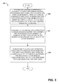
- FIGS. 3-6 illustrate flow diagrams of example, non-limiting embodiments of methods facilitating stashing in multi-level cache memory architectures in SoCs in accordance with an aspect described herein.
- FIG. 7 illustrates a block diagram of an example electronic computing environment that can be implemented to facilitate stashing for in multi-level cache memory architectures in an SoC in accordance with an aspect described herein.
- FIG. 1 is a block diagram illustrating an example, non-limiting embodiment of an SoC for which stashing in multi-level cache memory architectures can be facilitated in accordance with one or more aspects described herein.
- FIG. 1 is a simplified subset of select components of a SoC shown merely for providing context for the embodiments described herein.
- alternative or additional components can be included in SoC 100 .
- SoC 100 can be a server and/or general processor and/or can include server and/or general processor functionality.
- SoC 100 can have SoC components including, but not limited to, one or more processors (e.g., central processing unit (CPU) cores 110 , 112 , 114 ), SoC memory 116 , graphics processing unit (GPU) 118 , radio component 120 , one or more CPU core cache memories (e.g., per processor cache memory 122 , shared CPU core cache memory 123 ), one or more cache memory control circuits (e.g., per processor cache memory control circuit 130 configured to control per processor cache memory 122 , and shared CPU core cache memory control circuit configured to control shared CPU core cache memory 123 ), memory controller 128 and/or input/output (I/O) agent 102 .
- processors e.g., central processing unit (CPU) cores 110 , 112 , 114
- SoC memory 116 e.g., graphics processing unit (GPU) 118
- radio component 120 e.g., one or more CPU core cache memories (e.g., per processor cache memory 122 ,
- the controller e.g., per processor cache memory control circuit 130
- the controller for the per processor CPU cache memory (e.g., per processor cache memory 122 ) can be distinct from the controller (e.g., shared CPU core cache memory control circuit 136 ) for the shared CPU core caches (e.g., shared CPU core cache memory 123 ).
- shared CPU core cache memory is or includes a cache memory that is shared by multiple processors (e.g., CPU cores 112 , 114 ).
- Per processor cache memory is or includes a cache memory that is used by only one processor (e.g., per processor cache memory 122 ).
- one or more (or, in some embodiments, each of) per processor cache memory control circuits and/or shared CPU core cache memory control circuits can include or be electrically and/or communicatively coupled to a stashing and prefetching control circuit (e.g., stashing and prefetching control circuitry 104 at per processor cache memory control circuit 130 and stashing and prefetching control circuitry 104 at shared CPU core cache memory control circuit 136 ).
- a stashing and prefetching control circuit e.g., stashing and prefetching control circuitry 104 at per processor cache memory control circuit 130 and stashing and prefetching control circuitry 104 at shared CPU core cache memory control circuit 136 ).
- one or more per processor cache memory control circuits on SoC 100 can include a prefetch/address stashing buffer (e.g., prefetch/address stashing buffer 132 ) that can be controlled by stashing and prefetching control circuitry 104 in some embodiments.
- prefetch/address stashing buffer 132 can be or include a prefetch buffer with stashing logic.
- the prefetching is performed as a result of an instruction that accesses the address in the prefetch/address stashing buffer 132 that results in prefetch logic in the prefetch/address stashing buffer being triggered to fetch the data from the shared CPU core cache memory 123 .
- one or more of SoC 100 components can be electrically and/or communicatively coupled to one another (e.g., via interface 106 ) to perform one or more functions of SoC 100 (e.g., to facilitate stashing and/or prefetching on SoC 100 ).
- various components are electrically and/or communicatively coupled to one another, there is no communication link/path between the per processor cache memories of Soc 100 and the shared CPU core cache memories of SoC 100 .
- one or more of the embodiments described herein can advantageously reduce latency in the SoC 100 notwithstanding there may be no direct communication link/path between the one or more per processor cache memories and the one or more shared CPU core cache memories.
- CPU cores 110 , 112 , 114 can be processors designed by ARM Holdings or processors having x86 architecture.
- one or more of CPU cores 110 , 112 , 114 can be 64-bit server on chip processor designed by ARM Holdings configured to provide server functionality via SoC 100 .
- SoC 100 can serve data to one or more clients.
- SoC 100 can be or be included in data center computers, cloud computing systems, embedded communication processors, enterprise servers (e.g., multiple processor server systems) or the like.
- SoC memory 116 can be any number of different types of memory including, but not limited to, read only memory (ROM), random access memory (RAM), flash memory and/or electrically erasable programmable read only memory (EEPROM).
- SoC memory 116 can be a computer-readable storage medium storing instructions, computer code and/or functions executable by CPU cores 110 , 112 , 114 .
- SoC memory 116 can store instructions, computer code and/or functions executable by CPU cores 110 , 112 , 114 described herein to facilitate any number of different data processing functions (e.g., data center operations, cloud computing, server operations or the like).
- Memory controller 128 includes circuitry that manages and/or controls the flow of data to and/or from SoC memory 116 .
- memory controller 128 includes logic for reading from and/or writing to SoC memory 116 .
- Radio component 120 can include circuitry configured to transmit and/or receive radio frequency (RF) signals to and/or from SoC 100 .
- radio component 120 can operate according to any number of different telecommunication protocols for communication of voice, video and/or data traffic.
- radio component 120 can operate according to Wireless Fidelity (Wi-Fi), 4G Long-Term Evolution (LTE) and/or BLUETOOTH® protocols.
- GPU 118 can include circuitry to process graphics information and/or create visual images for output to a display component of a device associated with SoC 100 .
- a CPU core can be associated with a specific CPU core cache memory that is accessed by and served by the CPU core.
- CPU core 110 can be associated with per processor cache memory 122 that is accessed by and served by CPU core 110 .
- one or more CPU core cache memories are shared cache memories accessible by two or more of the CPU cores over a public bus interface (e.g., interface 106 ) to enable data to be shared amongst more than one CPU core.
- a public bus interface e.g., interface 106
- stashing support is provided for per processor cache memories (e.g., per processor cache memory 122 ) and/or for shared CPU core cache memories (e.g., shared CPU core cache memory 123 ).
- embodiments described herein can include multiple levels of cache memory. For example, three different types of cache memories, L1, L2 and L3, of different levels, can be employed in different embodiments.
- a per processor cache memory as described herein can be an L1 cache memory in some embodiments. Ideally, information is stored in the L1 cache memory. However, the L1 per processor cache memory is typically very small due to complexity, and therefore a more efficient location for storage of data is an L2 shared CPU core cache memory (e.g., shared CPU core cache memory 123 ).
- L1 per processor cache memory there is an L1 per processor cache memory and an L2 shared CPU core cache memory.
- the SoC includes three levels of cache memory (e.g., L1, L2 and L3 cache memories)
- L1 and L2 can be per processor cache memories and the L3 cache memory can be a shared CPU core cache memory.
- shared CPU core cache memories can be L2 and/or L3 cache memories while L1 cache memories can be per processor cache memories.
- Per processor cache memories and shared CPU core cache memories are each divided into a number of cache memory lines (or cache lines), with one or more, or each, cache memory line having an address and storing particular data of a determined size (e.g., 16 to 128 bytes of data).
- a CPU core e.g., CPU core 110
- the cache memory control circuit e.g., per processor cache memory control circuit 130
- the SoC 100 can perform stashing and/or prefetching operations to facilitate access to the data by the CPU core. If/when the CPU core (e.g., CPU core 110 ) requests the data at the address again, the contents at this address associated with the cache line will be in the cache memory used by the particular CPU core (e.g., per processor cache memory 122 ) already and the data can be retrieved from the cache memory (per processor cache memory 122 ) with reduced latency.
- the CPU core e.g., CPU core 110
- the contents at this address associated with the cache line will be in the cache memory used by the particular CPU core (e.g., per processor cache memory 122 ) already and the data can be retrieved from the cache memory (per processor cache memory 122 ) with reduced latency.
- stashing and prefetching control circuitry 104 can be configured to perform various different embodiments of stashing and/or prefetching.
- stashing and prefetching control circuitry 104 can generate signals for control of combination stashing data into one or more of CPU cache memories (e.g., per processor cache memory 122 and/or shared CPU core cache memory 123 ) and/or prefetching data into CPU cache memories for reduced latency.
- the stashing and/or prefetching do not require apriori knowledge of the particular CPU core on which software will be executed on the SoC.
- I/O Agent 102 can include circuitry facilitating communication between one or more components on SoC 100 .
- I/O Agent 102 can also include circuitry facilitating communication between SoC 100 and one or more peripheral components (not shown) communicatively coupled to SoC 100 .
- a stash request is consumed in a shared CPU core cache memory (e.g., shared CPU core cache memory 123 ).
- data associated with the stash request is written in the shared CPU core cache memory 123 .
- the address at which the data is written in the shared CPU core cache memory 123 is also written in the shared CPU core cache memory 123 .
- the address at which the data is written into the shared CPU core cache memory 123 is also written into one or more of the per processor cache memories (e.g., per processor cache memory 122 ).
- I/O agent 102 can write the data into a shared CPU core cache memory (e.g., shared CPU core cache memory 123 ).
- the I/O agent 102 can also write into the shared CPU core cache memory 123 , the cache line address at which the data is stored in the shared CPU core cache memory 123 .
- the address of the cache line at which the data is stored in shared CPU core cache memory 123 can also be stashed into a prefetch/address stashing buffer associated with the per processor cache memory control circuit 130 (e.g., prefetch/address stashing buffer 132 ) and/or at the per processor cache memory associated with the per processor cache memory control circuit 130 (e.g., per processor cache memory 122 ).
- the address can be stashed at the prefetch/address stashing buffer concurrent with, or in response to, or based on, stashing the data and/or address into shared CPU core cache memory 123 .
- the data stashed into shared CPU core cache memory 123 need not be written into each per processor cache memory 122 . Instead, the address for the cache line into which the data is written to the shared CPU core cache memory 123 can be written into the corresponding prefetch/address stashing buffer (e.g., prefetch/address stashing buffer 132 ) for the per processor cache memory control circuit 130 and/or at the per processor cache memory associated with the per processor cache memory control circuit 130 (e.g., per processor cache memory 122 ).
- prefetch/address stashing buffer e.g., prefetch/address stashing buffer 132
- the data and the address are stashed into a shared CPU core cache memory (e.g., shared CPU core cache memory 123 ) and a request is sent to the per processor cache memory control circuit 130 to write the address of the data into prefetch/address stashing buffer 132 and/or at the per processor cache memory associated with the per processor cache memory control circuit 130 (e.g., per processor cache memory 122 ).
- a shared CPU core cache memory e.g., shared CPU core cache memory 123
- a request is sent to the per processor cache memory control circuit 130 to write the address of the data into prefetch/address stashing buffer 132 and/or at the per processor cache memory associated with the per processor cache memory control circuit 130 (e.g., per processor cache memory 122 ).
- the prefetch access of the data associated with the address can be triggered by the prefetch/address stashing buffer or from the stashing and prefetching control circuitry 104 to prefetch the data from the shared CPU core cache memory 123 into the local cache memory for CPU core 110 (e.g., into per processor cache memory 122 ) to enable the load to be performed.
- the embodiment described can be advantageous because there can be many L1 on SoC 100 .
- One or more of the embodiments can initially store the data in the L2 cache (e.g., shared CPU core cache memory 123 ). After storing the data into the L2 cache, the address of the cache line where the data is located can be stashing into a prefetch/address stashing buffer associated with the L1 cache (e.g., prefetch/address stashing buffer 132 ).
- L2 shared cache CPU core cache memory e.g., shared CPU core cache memory
- L1 per processor cache memory e.g., per processor cache memory 122
- I/O agent 102 in response to, concurrent with, or based on stashing the data and address into shared CPU core cache memory 123 , I/O agent 102 can stash the address for the data into two or more (or, in some embodiments, all) prefetch/address stashing buffers for the per processor cache memories of the SoC 100 .
- the address can be broadcast to two or more (or, in some embodiments, all) prefetch/address stashing buffers for the per processor cache memories of the SoC 100 .
- the particular prefetch/address stashing buffer for that particular CPU core e.g., prefetch/address stashing buffer 132
- the per processor cache memory e.g., per processor cache memory 122
- prefetch/address stashing buffer 132 can prefetch a set of data including, the data requested and other data having a relationship with the data requested. For example, if the data requested is first data and the other data is second data, the total data prefetched can be the first data and the second data. The second data can be data located at a set of addresses that are sequential to the address for the first data.
- knowledge of which of the L1 per processor cache memories into which to stash data can be determined. The approach can then be performed of prefetching subsequent addresses for the different per processor cache memories.
- stashing and prefetching can be performed concurrently or at distinct time periods.
- data necessary for a next set of steps can be prefetched and stored in a particular per processor cache memory prior to being needed by the CPU core associated with the per processor cache memory.
- the prefetching can be performed if a particular condition is met. For example, an L1 per processor cache memory can be monitored to determine whether the data hit/needed by a corresponding CPU core is already stored in the L1 per processor cache memory cache memory. If not, a command can be issued to cause the data to be prefetched into the L1 per processor cache memory.
- FIG. 2 is a block diagram illustrating an example, non-limiting embodiment of stashing in accordance with one or more aspects described herein.
- the L1 and L2 cache memories are per processor cache memories while the L3 cache memory is a shared CPU cache memory. Repetitive description of like elements employed in respective embodiments of systems and/or apparatus described herein are omitted for sake of brevity. Similar to that described for FIG. 1 , the address for the cache line (and the data for which the I/O agent 102 issues a write request) can be stashed in the shared CPU cache memory 202 .
- the I/O agent 102 can also stash the cache line address into one or more of the CPU core cache memory or shared CPU core cache memories shown.
- one of CPU core cache memory or shared CPU core cache memories shown can be per processor cache memory 122 .
- method 300 can include storing, by a device including a plurality of multi-processor central processing unit cores, into a shared CPU core cache memory, first data and an address of first data, wherein the first data is requested from an input/output agent via a write request to a defined per processor cache memory control circuit of the device.
- method 300 can include stashing, by the device, into a prefetch/address stashing buffer for a defined per processor cache memory, an address of first data stored in the shared cache memory of a plurality of cache memories.
- method 300 can include in response to a CPU load operation indicating the address associated with the first data, prefetching, from the shared cache to the particular defined per processor cache memory associated with the CPU that performs the load operation, the first data.
- FIG. 4 illustrates a flow diagram of an example, non-limiting embodiment of a method facilitating stashing in multi-level cache memory architectures in accordance with an aspect described herein.
- method 400 can include stashing, by a device including a plurality of multi-processor central processing unit cores, first data into a first cache memory of a plurality of cache memories, wherein the plurality of cache memories are associated with a multi-level cache memory architecture.
- method 400 can include determining that the first data will be executed on a selected multi-processor central processing unit core of the plurality of multi-processor central processing unit cores, the selected multi-processor central processing unit core being associated with a second cache memory, the determining being based on a detected request for an address associated with the first data from the selected multi-processor central processing unit core.
- method 400 can include prefetching second data into the second cache memory of the plurality of cache memories, the second data including the first data and other data associated with a set of addresses relative to the address for the first data.
- the set of addresses is located at a first location and the address for the first data is located at a second location. The first location is subsequent to the second location. In some embodiments, the set of addresses includes a set of addresses in sequential order after the address for the first data.
- FIG. 5 illustrates a flow diagram of an example, non-limiting embodiment of a method facilitating stashing in multi-level cache memory architectures in accordance with an aspect described herein.
- method 500 can include stashing, by a device including a plurality of multi-processor central processing unit cores, first data into a first cache memory of a plurality of cache memories, wherein the first cache memory is a shared CPU core cache memory.
- method 500 can include generating control information including a first instruction to cause monitoring contents of a second cache memory of the plurality of cache memories to determine whether a defined condition is satisfied for the second cache memory.
- method 500 can include prefetching the first data from the first cache memory to the second cache memory based on execution of the first instruction.
- the prefetch/address stashing buffer includes prefetch logic that causes the prefetch/address stashing buffer to prefetch the first data from the first cache memory as a result, or side effect, of the execution of the first instruction.
- the stashing and the generating are performed concurrently.
- the second cache memory can be a per processor cache memory and the first cache can be a per processor cache memory.
- FIG. 6 illustrates a flow diagram of an example, non-limiting embodiment of a method facilitating stashing in multi-level cache memory architectures in accordance with an aspect described herein.
- method 600 can include generating a signal to cause first data and a first address for the first data to be stashed into a first cache memory of a plurality of cache memories.
- method 600 can include fetching data at the first address to be executed on a particular defined multi-processor central processing unit core of the plurality of multi-processor central processing unit cores, wherein the fetching is in response to a determination that the defined multi-processor central processing unit core has requested the data at the first address.
- the first data can include an instruction to be executed on the defined multi-processor central processing unit core.
- method 400 can include prefetching a set of addresses located subsequent to the first address, wherein the prefetching is performed in response to initiation of the fetching.
- the set of addresses include instructions to be executed on the defined multi-processor central processing unit core.
- the fetching and prefetching are performed concurrently. In some embodiments, the fetching and the prefetching are performed based on the determination that the defined multi-processor central processing unit core has requested the first address.
- the techniques described herein can be applied to any device and/or network in which reduced latency via stashing is desirable in a multi-processor system. It is to be understood, therefore, that handheld, portable and other computing devices and computing objects of all kinds are contemplated for use in connection with the various non-limiting embodiments. Accordingly, the computer/device described below in FIG. 7 is but one example, and the disclosed subject matter can be implemented with any client having network/bus interoperability and interaction. Thus, the disclosed subject matter can be implemented in an environment of networked hosted services in which very little or minimal client resources are implicated, e.g., a networked environment in which the client device serves merely as an interface to the network/bus, such as an object placed in an appliance.
- aspects of the disclosed subject matter can partly be implemented via an operating system, for use by a developer of services for a device or object, and/or included within application software that operates in connection with the component(s) of the disclosed subject matter.
- Software may be described in the general context of computer executable instructions, such as program modules or components, being executed by one or more computer(s), such as projection display devices, viewing devices, or other devices.
- computer(s) such as projection display devices, viewing devices, or other devices.
- FIG. 7 illustrates a block diagram of an example electronic computing environment that can be implemented to facilitate stashing in multi-level cache memory architectures in an SoC in accordance with an aspect described herein.
- FIG. 7 therefore illustrates an example of a suitable computing system environment 700 in which some aspects of the disclosed subject matter can be implemented, although as made clear above, the computing system environment 700 is only one example of a suitable computing environment for a device and is not intended to suggest any limitation as to the scope of use or functionality of the disclosed subject matter. Neither should the computing environment 700 be interpreted as having any dependency or requirement relating to any one or combination of components illustrated in the exemplary operating environment 700 .
- an exemplary device for implementing the disclosed subject matter includes a computing device in the form of a computer 710 .
- Components of computer 710 may include, but are not limited to, a processing unit 720 , a memory 730 , and a system bus 790 that couples various system components including the system memory 730 to the processing unit 720 .
- the system bus 790 may be any of several types of bus structures including a memory bus or memory controller, a peripheral bus, and a local bus using any of a variety of bus architectures.
- Computer 710 typically includes a variety of computer readable media.
- Computer readable media can be any available media that can be accessed by computer 710 .
- the computer readable media can be non-transitory computer readable storage media.
- computer readable media can comprise computer storage media and communication media.
- Computer storage media includes volatile and nonvolatile, removable and non-removable media implemented in any method or technology for storage of information such as computer readable instructions, data structures, program modules or other data.
- Computer storage media includes, but is not limited to, RAM, ROM, EEPROM, flash memory or other memory technology, compact disk read only memory (CD-ROM), digital versatile disks (DVD) or other optical disk storage, magnetic cassettes, magnetic tape, magnetic disk storage or other magnetic storage devices, or any other medium which can be used to store the desired information and which can be accessed by computer 710 .
- Communication media typically embodies computer readable instructions, data structures, program modules, or other data in a modulated data signal such as a carrier wave or other transport mechanism and includes any information delivery media.
- the memory 730 may include computer storage media in the form of volatile and/or nonvolatile memory such as ROM and/or RAM.
- a basic input/output system (BIOS) containing the basic routines that help to transfer information between elements within computer 710 , such as during start-up, may be stored in memory 730 .
- BIOS basic input/output system
- Memory 730 typically also contains data and/or program modules that are immediately accessible to and/or presently being operated on by processing unit 720 .
- memory 730 may also include an operating system, application programs, other program modules, and program data.
- the computer 710 may also include other removable/non-removable, volatile/nonvolatile computer storage media.
- computer 710 could include a hard disk drive that reads from or writes to non-removable, nonvolatile magnetic media, a magnetic disk drive that reads from or writes to a removable, nonvolatile magnetic disk, and/or an optical disk drive that reads from or writes to a removable, nonvolatile optical disk, such as a CD-ROM or other optical media.
- Other removable/non-removable, volatile/nonvolatile computer storage media that can be used in the exemplary operating environment include, but are not limited to, magnetic tape cassettes, flash memory cards, digital versatile disks, digital video tape, solid state RAM, solid state ROM, and the like.
- a hard disk drive is typically connected to the system bus 790 through a non-removable memory interface such as an interface
- a magnetic disk drive or optical disk drive is typically connected to the system bus 790 by a removable memory interface, such as an interface.
- a user can enter commands and information into the computer 710 through input devices such as a keyboard and pointing device, commonly referred to as a mouse, trackball, or touch pad.
- Other input devices can include a microphone, joystick, game pad, satellite dish, scanner, wireless device keypad, voice commands, or the like.
- These and other input devices are often connected to the processing unit 720 through user input 740 and associated interface(s) that are coupled to the system bus 790 , but may be connected by other interface and bus structures, such as a parallel port, game port, or a universal serial bus (USB).
- a graphics subsystem can also be connected to the system bus 790 .
- a projection unit in a projection display device, or a heads up display (HUD) in a viewing device or other type of display device can also be connected to the system bus 790 via an interface, such as output interface 750 , which may in turn communicate with video memory.
- an interface such as output interface 750
- computers can also include other peripheral output devices such as speakers which can be connected through output interface 750 .
- the computer 710 can operate in a networked or distributed environment using logical connections to one or more other remote computer(s), such as remote computer 770 , which can in turn have media capabilities different from device 710 .
- the remote computer 770 can be a personal computer, a server, a router, a network personal computer (PC), a peer device, personal digital assistant (PDA), cell phone, handheld computing device, a projection display device, a viewing device, or other common network node, or any other remote media consumption or transmission device, and may include any or all of the elements described above relative to the computer 710 .
- network 7 include a network 780 , such local area network (LAN) or a wide area network (WAN), but can also include other networks/buses, either wired or wireless.
- LAN local area network
- WAN wide area network
- Such networking environments are commonplace in homes, offices, enterprise-wide computer networks, intranets and the Internet.
- the computer 710 When used in a LAN networking environment, the computer 710 can be connected to the LAN 780 through a network interface 760 or adapter. When used in a WAN networking environment, the computer 710 can typically include a communications component, such as a modem, or other means for establishing communications over the WAN, such as the Internet.
- a communications component such as wireless communications component, a modem and so on, which can be internal or external, can be connected to the system bus 790 via the user input interface of input 740 , or other appropriate mechanism.
- program modules depicted relative to the computer 710 can be stored in a remote memory storage device. It will be appreciated that the network connections shown and described are exemplary and other means of establishing a communications link between the computers can be used.
- a component can be one or more transistors, a memory cell, an arrangement of transistors or memory cells, a gate array, a programmable gate array, an application specific integrated circuit, a controller, a processor, a process running on the processor, an object, executable, program or application accessing or interfacing with semiconductor memory, a computer, or the like, or a suitable combination thereof.
- the component can include erasable programming (e.g., process instructions at least in part stored in erasable memory) or hard programming (e.g., process instructions burned into non-erasable memory at manufacture).
- an architecture can include an arrangement of electronic hardware (e.g., parallel or serial transistors), processing instructions and a processor, which implement the processing instructions in a manner suitable to the arrangement of electronic hardware.
- an architecture can include a single component (e.g., a transistor, a gate array, . . . ) or an arrangement of components (e.g., a series or parallel arrangement of transistors, a gate array connected with program circuitry, power leads, electrical ground, input signal lines and output signal lines, and so on).
- a system can include one or more components as well as one or more architectures.
- One example system can include a switching block architecture comprising crossed input/output lines and pass gate transistors, as well as power source(s), signal generator(s), communication bus(ses), controllers, I/O interface, address registers, and so on. It is to be appreciated that some overlap in definitions is anticipated, and an architecture or a system can be a stand-alone component, or a component of another architecture, system, etc.
- the disclosed subject matter can be implemented as a method, apparatus, or article of manufacture using typical manufacturing, programming or engineering techniques to produce hardware, firmware, software, or any suitable combination thereof to control an electronic device to implement the disclosed subject matter.
- the terms “apparatus” and “article of manufacture” where used herein are intended to encompass an electronic device, a semiconductor device, a computer, or a computer program accessible from any computer-readable device, carrier, or media.
- Computer-readable media can include hardware media, or software media.
- the media can include non-transitory media, or transport media.
- non-transitory media can include computer readable hardware media.
- Computer readable hardware media can include but are not limited to magnetic storage devices (e.g., hard disk, floppy disk, magnetic strips . . . ), optical disks (e.g., compact disk (CD), digital versatile disk (DVD) . . . ), smart cards, and flash memory devices (e.g., card, stick, key drive . . . ).
- Computer-readable transport media can include carrier waves, or the like.
- exemplary is used herein to mean serving as an example, instance, or illustration. Any aspect or design described herein as “exemplary” is not necessarily to be construed as preferred or advantageous over other aspects or designs. Rather, use of the word exemplary is intended to present concepts in a concrete fashion.
- the terms (including a reference to a “means”) used to describe such components are intended to correspond, unless otherwise indicated, to any component which performs the specified function of the described component (e.g., a functional equivalent), even though not structurally equivalent to the disclosed structure, which performs the function in the herein illustrated exemplary aspects of the embodiments.
- a particular feature may have been disclosed with respect to only one of several implementations, such feature may be combined with one or more other features of the other implementations as may be desired and advantageous for any given or particular application.
- the embodiments include a system as well as a computer-readable medium having computer-executable instructions for performing the acts and/or events of the various processes.
Abstract
Description
Claims (19)
Priority Applications (2)
| Application Number | Priority Date | Filing Date | Title |
|---|---|---|---|
| US14/796,167 US9720830B2 (en) | 2015-07-10 | 2015-07-10 | Systems and methods facilitating reduced latency via stashing in system on chips |
| PCT/US2015/042791 WO2017011021A1 (en) | 2015-07-10 | 2015-07-30 | Systems and methods facilitating reduced latency via stashing in systems on chips |
Applications Claiming Priority (1)
| Application Number | Priority Date | Filing Date | Title |
|---|---|---|---|
| US14/796,167 US9720830B2 (en) | 2015-07-10 | 2015-07-10 | Systems and methods facilitating reduced latency via stashing in system on chips |
Publications (2)
| Publication Number | Publication Date |
|---|---|
| US20170010966A1 US20170010966A1 (en) | 2017-01-12 |
| US9720830B2 true US9720830B2 (en) | 2017-08-01 |
Family
ID=57730322
Family Applications (1)
| Application Number | Title | Priority Date | Filing Date |
|---|---|---|---|
| US14/796,167 Active 2035-09-29 US9720830B2 (en) | 2015-07-10 | 2015-07-10 | Systems and methods facilitating reduced latency via stashing in system on chips |
Country Status (2)
| Country | Link |
|---|---|
| US (1) | US9720830B2 (en) |
| WO (1) | WO2017011021A1 (en) |
Families Citing this family (3)
| Publication number | Priority date | Publication date | Assignee | Title |
|---|---|---|---|---|
| TWI680375B (en) * | 2018-08-23 | 2019-12-21 | 慧榮科技股份有限公司 | Multi-processor system having distributed mailbox architecture and processor error checking method thereof |
| US11263137B2 (en) * | 2020-05-27 | 2022-03-01 | Arm Limited | Core-to-core cache stashing and target discovery |
| US11314645B1 (en) * | 2020-12-16 | 2022-04-26 | Arm Limited | Cache stash relay |
Citations (13)
| Publication number | Priority date | Publication date | Assignee | Title |
|---|---|---|---|---|
| EP1217526A1 (en) | 2000-12-21 | 2002-06-26 | Texas Instruments Incorporated | Multilevel cache architecture and data transfer |
| US6446167B1 (en) | 1999-11-08 | 2002-09-03 | International Business Machines Corporation | Cache prefetching of L2 and L3 |
| US6924810B1 (en) | 1998-10-09 | 2005-08-02 | Advanced Micro Devices, Inc. | Hierarchical texture cache |
| US20100125677A1 (en) * | 2008-11-17 | 2010-05-20 | Bouvier Daniel L | Cache Stashing Processor Control Messages |
| US7773597B2 (en) | 2005-04-20 | 2010-08-10 | Cisco Technology, Inc. | Method and system for dynamic stashing for cryptographic operations using beginning packet information |
| US20120226865A1 (en) * | 2009-11-26 | 2012-09-06 | Snu R&Db Foundation | Network-on-chip system including active memory processor |
| US8370294B2 (en) | 2009-05-06 | 2013-02-05 | Microsoft Corporation | File stashing for storage media |
| US8429315B1 (en) * | 2011-06-24 | 2013-04-23 | Applied Micro Circuits Corporation | Stashing system and method for the prevention of cache thrashing |
| US20130268822A1 (en) * | 2012-04-04 | 2013-10-10 | University Of Southern California | Correctable parity protected memory |
| US8671232B1 (en) | 2013-03-07 | 2014-03-11 | Freescale Semiconductor, Inc. | System and method for dynamically migrating stash transactions |
| US8924784B2 (en) | 2012-04-12 | 2014-12-30 | Freescale Semiconductor, Inc. | Controller for managing a reset of a subset of threads in a multi-thread system |
| US9336162B1 (en) * | 2012-02-16 | 2016-05-10 | Applied Micro Circuits Corporation | System and method for pre-fetching data based on a FIFO queue of packet messages reaching a first capacity threshold |
| US20160154737A1 (en) * | 2014-11-29 | 2016-06-02 | Vakul Garg | System for pre-fetching data frames using hints from work queue scheduler |
-
2015
- 2015-07-10 US US14/796,167 patent/US9720830B2/en active Active
- 2015-07-30 WO PCT/US2015/042791 patent/WO2017011021A1/en active Application Filing
Patent Citations (14)
| Publication number | Priority date | Publication date | Assignee | Title |
|---|---|---|---|---|
| US6924810B1 (en) | 1998-10-09 | 2005-08-02 | Advanced Micro Devices, Inc. | Hierarchical texture cache |
| US6446167B1 (en) | 1999-11-08 | 2002-09-03 | International Business Machines Corporation | Cache prefetching of L2 and L3 |
| EP1217526A1 (en) | 2000-12-21 | 2002-06-26 | Texas Instruments Incorporated | Multilevel cache architecture and data transfer |
| US7773597B2 (en) | 2005-04-20 | 2010-08-10 | Cisco Technology, Inc. | Method and system for dynamic stashing for cryptographic operations using beginning packet information |
| US20100125677A1 (en) * | 2008-11-17 | 2010-05-20 | Bouvier Daniel L | Cache Stashing Processor Control Messages |
| US7774522B2 (en) * | 2008-11-17 | 2010-08-10 | Applied Micro Circuits Corporation | Cache stashing processor control messages |
| US8370294B2 (en) | 2009-05-06 | 2013-02-05 | Microsoft Corporation | File stashing for storage media |
| US20120226865A1 (en) * | 2009-11-26 | 2012-09-06 | Snu R&Db Foundation | Network-on-chip system including active memory processor |
| US8429315B1 (en) * | 2011-06-24 | 2013-04-23 | Applied Micro Circuits Corporation | Stashing system and method for the prevention of cache thrashing |
| US9336162B1 (en) * | 2012-02-16 | 2016-05-10 | Applied Micro Circuits Corporation | System and method for pre-fetching data based on a FIFO queue of packet messages reaching a first capacity threshold |
| US20130268822A1 (en) * | 2012-04-04 | 2013-10-10 | University Of Southern California | Correctable parity protected memory |
| US8924784B2 (en) | 2012-04-12 | 2014-12-30 | Freescale Semiconductor, Inc. | Controller for managing a reset of a subset of threads in a multi-thread system |
| US8671232B1 (en) | 2013-03-07 | 2014-03-11 | Freescale Semiconductor, Inc. | System and method for dynamically migrating stash transactions |
| US20160154737A1 (en) * | 2014-11-29 | 2016-06-02 | Vakul Garg | System for pre-fetching data frames using hints from work queue scheduler |
Non-Patent Citations (1)
| Title |
|---|
| International Search Report & Written Opinion for PCT Application Serial No. PCT/US2015/042791, mailed Apr. 8, 2016, 11 pages. |
Also Published As
| Publication number | Publication date |
|---|---|
| WO2017011021A1 (en) | 2017-01-19 |
| US20170010966A1 (en) | 2017-01-12 |
Similar Documents
| Publication | Publication Date | Title |
|---|---|---|
| US20190212801A1 (en) | Enabling A Non-Core Domain To Control Memory Bandwidth | |
| US20190172538A1 (en) | Hybrid memory architectures | |
| RU2483347C2 (en) | Caching apparatus, method and system | |
| US11526440B2 (en) | Providing multiple memory modes for a processor including internal memory | |
| US9881680B2 (en) | Multi-host power controller (MHPC) of a flash-memory-based storage device | |
| US9632958B2 (en) | System for migrating stash transactions | |
| US9632953B2 (en) | Providing input/output virtualization (IOV) by mapping transfer requests to shared transfer requests lists by IOV host controllers | |
| US10613984B2 (en) | Prefetch tag for eviction promotion | |
| US9720830B2 (en) | Systems and methods facilitating reduced latency via stashing in system on chips | |
| US20190042415A1 (en) | Storage model for a computer system having persistent system memory | |
| US9880849B2 (en) | Allocation of load instruction(s) to a queue buffer in a processor system based on prediction of an instruction pipeline hazard | |
| US8661169B2 (en) | Copying data to a cache using direct memory access | |
| US10339065B2 (en) | Optimizing memory mapping(s) associated with network nodes | |
| US10310857B2 (en) | Systems and methods facilitating multi-word atomic operation support for system on chip environments | |
| US9229757B2 (en) | Optimizing a file system interface in a virtualized computing environment | |
| US9792207B2 (en) | Data storage in a mobile device with embedded mass storage device | |
| US10180904B2 (en) | Cache memory and operation method thereof | |
| US20210224213A1 (en) | Techniques for near data acceleration for a multi-core architecture | |
| KR20230041593A (en) | Scalable address decoding scheme for cxl type-2 devices with programmable interleave granularity | |
| US11093401B2 (en) | Hazard prediction for a group of memory access instructions using a buffer associated with branch prediction | |
| US20170153994A1 (en) | Mass storage region with ram-disk access and dma access | |
| US8510605B2 (en) | Computer system inspecting defective cell and control method thereof | |
| US20230297632A1 (en) | Fetching a query result using a query filter | |
| US20230333858A1 (en) | Methods and apparatus to boot from block devices | |
| EP3869344A1 (en) | Technology to ensure sufficient memory type range registers to fully cache complex memory configurations |
Legal Events
| Date | Code | Title | Description |
|---|---|---|---|
| AS | Assignment |
Owner name: APPLIED MICRO CIRCUITS CORPORATION, CALIFORNIA Free format text: ASSIGNMENT OF ASSIGNORS INTEREST;ASSIGNOR:MITTAL, MILLIND;REEL/FRAME:036057/0498 Effective date: 20150617 |
|
| AS | Assignment |
Owner name: MACOM CONNECTIVITY SOLUTIONS, LLC, MASSACHUSETTS Free format text: MERGER AND CHANGE OF NAME;ASSIGNORS:APPLIED MICRO CIRCUITS CORPORATION;MACOM CONNECTIVITY SOLUTIONS, LLC;MACOM CONNECTIVITY SOLUTIONS, LLC;SIGNING DATES FROM 20170126 TO 20170127;REEL/FRAME:042176/0185 |
|
| AS | Assignment |
Owner name: GOLDMAN SACHS BANK USA, AS COLLATERAL AGENT, NEW Y Free format text: SECURITY INTEREST;ASSIGNOR:MACOM CONNECTIVITY SOLUTIONS, LLC (SUCCESSOR TO APPLIED MICRO CIRCUITS CORPORATION);REEL/FRAME:042444/0891 Effective date: 20170504 Owner name: GOLDMAN SACHS BANK USA, AS COLLATERAL AGENT, NEW YORK Free format text: SECURITY INTEREST;ASSIGNOR:MACOM CONNECTIVITY SOLUTIONS, LLC (SUCCESSOR TO APPLIED MICRO CIRCUITS CORPORATION);REEL/FRAME:042444/0891 Effective date: 20170504 |
|
| STCF | Information on status: patent grant |
Free format text: PATENTED CASE |
|
| AS | Assignment |
Owner name: MACOM CONNECTIVITY SOLUTIONS, LLC (SUCCESSOR TO APPLIED MICRO CIRCUITS CORPORATION), MASSACHUSETTS Free format text: RELEASE BY SECURED PARTY;ASSIGNOR:GOLDMAN SACHS BANK USA, AS COLLATERAL AGENT;REEL/FRAME:044652/0609 Effective date: 20171027 Owner name: MACOM CONNECTIVITY SOLUTIONS, LLC (SUCCESSOR TO AP Free format text: RELEASE BY SECURED PARTY;ASSIGNOR:GOLDMAN SACHS BANK USA, AS COLLATERAL AGENT;REEL/FRAME:044652/0609 Effective date: 20171027 |
|
| AS | Assignment |
Owner name: PROJECT DENVER INTERMEDIATE HOLDINGS LLC, CALIFORNIA Free format text: ASSIGNMENT OF ASSIGNORS INTEREST;ASSIGNOR:MACOM CONNECTIVITY SOLUTIONS, LLC;REEL/FRAME:044798/0599 Effective date: 20171025 Owner name: PROJECT DENVER INTERMEDIATE HOLDINGS LLC, CALIFORN Free format text: ASSIGNMENT OF ASSIGNORS INTEREST;ASSIGNOR:MACOM CONNECTIVITY SOLUTIONS, LLC;REEL/FRAME:044798/0599 Effective date: 20171025 |
|
| AS | Assignment |
Owner name: AMPERE COMPUTING LLC, CALIFORNIA Free format text: CHANGE OF NAME;ASSIGNOR:PROJECT DENVER INTERMEDIATE HOLDINGS LLC;REEL/FRAME:044717/0683 Effective date: 20171129 |
|
| FEPP | Fee payment procedure |
Free format text: ENTITY STATUS SET TO SMALL (ORIGINAL EVENT CODE: SMAL) |
|
| FEPP | Fee payment procedure |
Free format text: ENTITY STATUS SET TO UNDISCOUNTED (ORIGINAL EVENT CODE: BIG.); ENTITY STATUS OF PATENT OWNER: LARGE ENTITY |
|
| MAFP | Maintenance fee payment |
Free format text: PAYMENT OF MAINTENANCE FEE, 4TH YEAR, LARGE ENTITY (ORIGINAL EVENT CODE: M1551); ENTITY STATUS OF PATENT OWNER: LARGE ENTITY Year of fee payment: 4 |