US9667291B2 - Unwanted component reduction system - Google Patents
Unwanted component reduction system Download PDFInfo
- Publication number
- US9667291B2 US9667291B2 US14/527,608 US201414527608A US9667291B2 US 9667291 B2 US9667291 B2 US 9667291B2 US 201414527608 A US201414527608 A US 201414527608A US 9667291 B2 US9667291 B2 US 9667291B2
- Authority
- US
- United States
- Prior art keywords
- signal
- unwanted
- frequency
- output
- filter
- Prior art date
- Legal status (The legal status is an assumption and is not a legal conclusion. Google has not performed a legal analysis and makes no representation as to the accuracy of the status listed.)
- Active
Links
Images


Classifications
-
- H—ELECTRICITY
- H04—ELECTRIC COMMUNICATION TECHNIQUE
- H04B—TRANSMISSION
- H04B1/00—Details of transmission systems, not covered by a single one of groups H04B3/00 - H04B13/00; Details of transmission systems not characterised by the medium used for transmission
- H04B1/06—Receivers
- H04B1/10—Means associated with receiver for limiting or suppressing noise or interference
- H04B1/12—Neutralising, balancing, or compensation arrangements
- H04B1/123—Neutralising, balancing, or compensation arrangements using adaptive balancing or compensation means
-
- H—ELECTRICITY
- H04—ELECTRIC COMMUNICATION TECHNIQUE
- H04L—TRANSMISSION OF DIGITAL INFORMATION, e.g. TELEGRAPHIC COMMUNICATION
- H04L23/00—Apparatus or local circuits for systems other than those covered by groups H04L15/00 - H04L21/00
Definitions
- This disclosure relates to an apparatus for and method of estimating a unwanted, often non-linear, component in a signal, and using the estimate to reduce the impact of the non-linear component.
- a received radio frequency (RF) signal is amplified and demodulated.
- This process often includes a frequency translation operation where the incoming signal is mixed with a locally generated signal. This enables subsequent amplification stages to be performed over a narrower pass band. This makes it easier to build amplifiers and other components with acceptable levels of distortion, noise and power consumption characteristics.
- non-linearity may still exist within the RF signal processing path and/or the baseband signal processing path. The non-linearity may result from the performance of real world transistors as opposed to ideal ones, or charging and discharging of explicit or parasitic capacitors in signal processing elements, such as analog to digital converters, giving rise to non-linearity.
- the present disclosure relates to a RF receiver system in which certain embodiments address some, and preferably all, of the above objectives.
- an apparatus for reducing the impact of an unwanted signal component on a wanted signal component comprises means for processing an input signal containing both the wanted signal component and potentially the unwanted signal component to create an estimated unwanted signal. The apparatus then compares the estimated unwanted signal with the input signal and/or an output signal to enable it to create a cancellation signal. The cancellation signal is combined with the input signal to partially or substantially cancel the unwanted signal component.
- the unwanted signal component may be a narrow band signal or a broadband signal.
- the apparatus may identify the narrowband unwanted signal and seek to minimize its influence on the output signal.
- the unwanted signal component may be generated as the result of non-linearity in a signal processing circuit giving rise to the generation of harmonic terms.
- the apparatus may deliberately apply equivalent non-linear processing to the input signal.
- Such non-linear processing may include forming the square of the input signal, the third power of the input signal and so on.
- the non-linearity may be estimated at a narrow or nominally a single frequency.
- a signal processing circuit such as a radio receiver
- the signal processing circuit may be arranged to estimate a correction signal for the second harmonic 2F B of the blocker signal. This may improve recovery of the wanted signal at F w when F w is substantially the same as 2F B .
- the signal processing circuit may estimate coefficients to be applied to the estimate of the unwanted signal to generate a correction signal.
- the correction signal may be generated by passing the estimated error signal through a filter.
- the filter may be finite impulse response (FIR) filter.
- Frequency translation of the unwanted frequency component may be performed in order to allow the filter to operate at a nominally constant frequency. Therefore, the filter taps and coefficients may remain the same when the apparatus is in use. Given that all of this signal processing may be done in the digital domain, i.e., frequency translation by multiplying with a repetitive waveform and filtering, the designer might choose to omit the frequency translation and instead retune the digital filter.
- the pressures to provide multi-mode and multi-frequency receivers are found in a number of operating environments.
- An example of such an environment is the mobile telephony space where devices may receive signals operating at one of a plurality of standards, such as 2G, 3G, 4G, LTE and so on.
- Each of these standards tends to be highly regulated, for example, in terms of required acceptance bandwidth, sensitivity, immunity to interfering signals and so on.
- a receiver including a circuit constituting an embodiment of the first aspect of this disclosure.
- a method of reducing an unwanted signal component within an output signal comprising receiving an input signal containing a wanted signal component and potentially an unwanted signal component; operating on the input signal to form an estimate of the unwanted signal component; generating a correction signal; combining the correction signal with the input signal; and monitoring the output signal to refine the correction signal so as to reduce the influence of the unwanted signal.
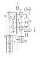
- FIG. 1 is a block diagram of a receiver operating at zero intermediate frequency
- FIG. 2 is a block diagram of a receiver that is configured to operate at a low intermediate frequency
- FIG. 3 schematically illustrates the transformation of a spectrum at the input of a receiver, in which the frequencies are referenced to a local oscillator, with the spectrum at to output of the receiver as a result of non-linearity within the receiver;
- FIG. 4 is a measured frequency response from a receiver where a large blocker is present and its second harmonic substantially coincides with a signal that it is desired to be received;
- FIG. 5 is a schematic diagram of a signal processing system for reducing an unwanted harmonic signal arising from a blocker
- FIG. 6 shows components of the signal processor of FIG. 5 in greater detail
- FIG. 7 shows components of an adaptation engine of FIG. 6 in greater detail
- FIG. 8 shows the narrowband filters of the adaptation engine of FIG. 7 in detail
- FIG. 9 shows further features of the adaptation engine of FIG. 7 in greater detail
- FIG. 10 shows the operation of the correlation engine of FIG. 9 ;
- FIG. 11 shows the operation of the matrix and vector build engine of FIG. 9 ;
- FIG. 12 shows the operation of the least squares engine of FIG. 9 ;
- FIG. 13 is a schematic diagram of a circuit operable to search for blocker signals or components resulting from the presence of a blocker signal
- FIG. 14 shows the apparatus of FIG. 13 in greater detail
- FIGS. 15 a to 15 c show an example of a frequency search
- FIG. 16 is a schematic diagram of a parametric engine that can be used to identify a blocker signal
- FIG. 17 shows an embodiment of a first order parametric engine
- FIG. 18 shows the circuit of FIG. 17 in association with a controller for providing timing and control signals.
- Such approaches enable integrated circuit providers to provide or propose integrated circuits where quadrature mixers, variable gain amplifiers, filters and analog to digital converters are provided on a single integrated circuit. Furthermore, digital domain signal processing can also be provided on the chip/integrated circuit to process the output of an analog to digital converter.
- the local oscillator for such a system may be provided ‘on chip’ as well, i.e., within the same circuit package.
- Such an integrated circuit can offer reduced cost through integration; greater ease of use for a customer as it moves closer to a system-on-chip style solution; and/or relaxation of RF signals processing and routing specifications and simplification of frequency planning. This is particularly relevant where several receivers are provided in close proximity.
- FIG. 1 is a schematic block diagram of a direct conversion receiver
- FIG. 2 is a schematic block diagram of a low IF receiver.
- the direct conversion receiver broadly comprises three functional blocks. As illustrated, the direct conversion receiver 10 of FIG. 1 comprises an RF amplification stage 12 , a filter 14 and a down-converter 16 .
- the RF amplification stage 12 receives a signal from an antenna 18 and provides a controllable gain, represented in FIG. 1 by a variable attenuator 20 and a low noise amplifier 22 .
- the output from the RF amplification stage 12 is band pass filtered, for example, by a surface acoustic wave (SAW) filter 14 .
- SAW surface acoustic wave
- Other filter technologies may alternatively or additionally be used.
- An output of the filter 14 is provided to a RF input of the down-converter 16 .
- the down-converter 16 comprises a quadrature mixer 30 which receives the amplified RF input signal at a mixer signal input, and mixes this with local oscillator (LO) signals supplied to local oscillator inputs of the mixer 30 .
- the local oscillator signal(s) are provided by a local oscillator 32 .
- the local oscillator 32 may be provided as an integrated component (in the same integrated circuit package as the mixer 30 ) or as a separate component.
- the output of the local oscillator 32 may be buffered by a buffer or amplifier 34 prior to being supplied to the mixer 30 .
- a quadrature mixer 30 typically comprises two mixers, one to work on an in-phase signal (or I channel) and one to work on signals whose phase is shifted by ⁇ /2 radians (90 degrees) relative to the in-phase signal, the quadrature channel (or Q channel).
- the LO signal from the local oscillator 32 can be generated as two LO signals of the same frequency but offset by 90 degrees, or the local oscillator signal can subsequently be processed to generate the two phase shifted local oscillator signals desired by a quadrature mixer 30 .
- the I and Q channels are typically approximately 90 degrees out of phase without each other and may not be exactly 90 degrees out of phase.
- the local oscillator signal can also be set to W C so that direct down conversion to DC/baseband is performed.
- Local oscillator signals of the desired frequency can be derived using phase locked loops and the like as known to the person skilled in the art.
- the I and Q channels from the mixer 30 may then be subjected to further gain, for example by a fixed gain amplifier 40 and a variable gain amplifier 42 , before being low pass filtered by a filter 44 to remove out of band interference, and then sent to an analog to digital converter 50 to digitize the I and Q channels.
- further gain for example by a fixed gain amplifier 40 and a variable gain amplifier 42 , before being low pass filtered by a filter 44 to remove out of band interference, and then sent to an analog to digital converter 50 to digitize the I and Q channels.
- the low IF receiver of FIG. 2 has similarities with the direct conversion receiver of FIG. 1 , and like parts have been shown using like reference numbers.
- the low IF receiver has two local oscillators.
- a second local oscillator can be provided to generate a second local oscillator frequency to enable a second mixer 62 to downconvert the signals to baseband prior to being passed through a low pass filter 64 .
- FIG. 2 includes a graph showing the frequency spectrum available at the output of the ADC 50 .
- the “baseband” may have a bandwidth of around 200 MHz.
- a bandwidth of about 75 MHz is desired.
- the first local oscillator 32 can be set to give a nominal first intermediate frequency inside the pass band, for example at about 150 MHz, and the second local oscillator 60 can act to down convert that to baseband.
- a desirable feature of a receiver is its ability to deal with the presence of a relatively strong interfering signal.
- An example of such a specification is the 3GPP TS 51.021 blocker test. In this test, a local blocking signal is introduced into the receiver with a strength of ⁇ 1 dBFS (one dB less than full scale signal strength). Any harmonics from mixing the blocker signal with the local oscillator signal should be at least 90 dB down on the blocker power, as part of the test specification.
- Non-linearities resulting in mixing or amplification stages can be regarded as RF non-linearities.
- Any non-linearity as a result of baseband components, such as the ADC 50 can be regarded as a baseband non-linearity.
- RF non-linearities and/or baseband non-linearities can be reduced and/or eliminated using embodiments of the apparatus disclosed here.
- baseband non-linearity for illustrative purposes.
- a suitable non-linearity model may include terms of the form
- a feature of using CMOS is that digital gates are relatively inexpensive and can be fabricated to perform additional processing of the signal from the ADC 50 . This can be exploited to correct impairments of the RF or analog components, and/or to remove interference received at the antenna 18 .
- a significant blocking signal can be observed in a mobile telephony system.
- the signal of interest e.g., a signal associated with a telephone call
- the signal of interest may occupy a frequency band centered around 2f 0 .
- the blocker happens to occur at a frequency f 0 .
- the actual frequencies of the blocker and the signal of interest are LO+f 0 and LO+2f 0 , respectively.
- f LO COS(2 ⁇ f LO t )
- f BLOCK COS(2 ⁇ f LO +f 0 ) t
- a harmonic of the blocker occurs at +2f 0 and at ⁇ 2f 0 with respect to the local oscillator frequency f LO .
- the blocker 2nd harmonic sits over the wanted signal which occurs at 2fo in the baseband.
- the blocker second harmonic which may be known as ‘HD 2 ’ by those skilled in the art is related to the blocker. If the relationship between the blocker second harmonic and the block can be estimated, then the blocker signal can be used to estimate a correction signal to reduce the second harmonic signal HD 2 , or indeed any desired harmonic of the blocker.
- FIG. 4 is a spectral diagram for a known low IF conversion receiver and ADC. The frequencies are shown with respect to the intermediate frequency which may typically be in the region of 75 MHz to 100 MHz.
- a blocker with a signal strength of ⁇ 2 dBFS occurs at ⁇ 18 MHz compared to the intermediate frequency (assuming that the local oscillator is on the low side of the incoming frequency).
- Second order harmonic distortion gives rise to harmonics at ⁇ 36 MHz, and +36 MHz compared to the intermediate frequency.
- a blocker image occurs at +18 MHz compared to the intermediate frequency and a third harmonic labelled HD 3 appears at +54 MHz but does not appear at ⁇ 54 MHz. This is a real artefact resulting from intermodulation between the various frequencies.
- the spectrum in FIG. 4 runs from IF ⁇ 65 MHz to IF+65 MHz. If, for numerical convenience the intermediate frequency, IF, was 100 MHz, then the spectrum would extend between 35 MHz and 165 MHz.
- the measured in band second harmonic signal (HD 2 ) had a power which is about 85 dB less than the blocker.
- a 0 , a 1 , a 2 , a 3 , a 4 , etc. are coefficients in a polynomial expansion representing the relative contribution of each of the polynomial terms to the output y. Distortion relating to any of these terms a 2 x 2 , a 3 x 3 , etc., and/or from intermodulation products may be estimated and reduced. However, as in the example given so far, the main source of distortion can be second order harmonic distortion. Accordingly, this case will be considered further.
- FIG. 5 shows a schematic representation of an apparatus that includes a second harmonic reducer 100 comprising a squarer 102 , a correction signal generator 104 and an adder 106 .
- reducers configured to suppress unwanted signals at other frequencies, such as other harmonics, can alternatively or additionally be implemented.
- the squarer 102 can be implemented in hardware as a two input digital multiplier.
- the squarer 102 can serve as a first processor configured to process the output y of the ADC 50 by operating on the output y with a function that includes a term descriptive of the unwanted signal component to create an estimated unwanted signal.
- the output of the squarer 102 is provided to the correction signal generator 104 , which receives an estimated correction coefficient â 2 .
- the apparatus can include a coefficient estimation circuit 107 configured to generate the estimated correction coefficient â 2 based on the output y of the ADC 50 .
- the coefficient estimation circuit 107 can serve as a second processor configured to process the estimated unwanted signal from the first processor and at least one of the output y from the ADC 50 or the output signal Z of the second harmonic reducer 110 to identify one or more parameters to apply to the estimated unwanted signal to generate a correction signal.
- the coefficient estimation circuit 107 can include a blocker detection engine and an adaptation engine, for example, as discussed below.
- a combiner such as the adder 106
- the residual amount of the second harmonic can depend on the accuracy of estimation of â 2 to reduce a 2 ⁇ â 2 .
- FIG. 6 is a block diagram of a second harmonic reduction circuit (or “reducer”) in association with a radio receiver, as might be found in a mobile receiver or a base station.
- a second harmonic reduction circuit or “reducer”
- the second harmonic reducer 100 is associated with a blocker detection engine 110 .
- the blocker detection engine 110 may be implemented in dedicated hardware, by a processor executing instructions stored in non-transitory computer-readable storage, or a combination of the same.
- the blocker detection engine 110 is connected to an adaptation engine 120 , which may be implemented in dedicated hardware, by a processor executing instructions stored in non-transitory computer-readable storage, or a combination of the same.
- the reducer 100 can run continuously while the ADC 50 is outputting data, whilst the blocker detection engine 110 and the adaptation engine 120 can be run intermittently.
- the output Z of the reducer 100 which represents the input data stream with a reduced unwanted signal component, is provided at output 101 .
- the correction signal generator 104 may be implemented as a buffer or delay line for maintaining a record of the most recent output N output words from the ADC 50 .
- the second harmonic reducer 100 works on the in-phase and quadrature signals. Many responses or transfer characteristics may be implemented in the second harmonic reducer 100 , which can be analogous in its construction to a finite impulse response (FIR) filter comprising M delay elements, such that an output p of the filter is represented by the following equation:
- FIR finite impulse response
- z ( n ) y ( n ) ⁇ a ( n ) ⁇ I 2 ( n )+ jQ 2 ( n ) ⁇ where a represent the filter coefficients.
- the second harmonic reducer 100 is responsive to an adaptation engine 120 , an embodiment of which is shown in greater detail in FIG. 7 .
- the adaptation engine 120 comprises tunable narrow band filters 130 and 132 , which are controlled by a blocker detection engine 110 , which will be described in greater detail later.
- the blocker detection engine 110 can set the centerband of the filters 130 and 132 at the frequency of the second order harmonic HD 2 .
- the input signal to the correction signal generator 104 and the output of the summer 106 are therefore filtered to extract the second harmonic terms of the blocker, and this information is used to update the coefficients used in a HD 2 model circuit 140 of the adaption engine 120 to set the coefficients to be applied to the taps of the correction signal generator 104 .
- the correction signal generator 104 is illustrated as a filter.
- the correction signal generator 104 can be a finite impulse response (FIR) filter in certain embodiments.
- FIR finite impulse response
- Such a filter can operate on both the I and Q channels, and may be a complex FIR filter (that is the filter receives both real and imaginary coefficients).
- a narrow band filter can be formed by multiplying the digitized output of the ADC 50 with a filter signal having a fundamental frequency matched or substantially matched to the frequency of the second harmonic HD 2 in the base band that arises from the blocker frequency.
- the filter signal can be formed as a digitally generated sinusoid (which may be represented as a complex number) and the multiplication, and hence mixing, can be performed in the digital domain.
- the filter signal can be implemented as a nominal square wave having magnitudes of +1 and ⁇ 1. This can allow the down conversion to be performed by a cyclical inversion of a sign bit. This multiplication and down conversion to DC is schematically illustrated in FIG. 8 .
- the second harmonic HD 2 (e.g., an I+jQ vector of samples corresponding to the signal content at the frequency HD 2 , in which j represents the square root of negative one) is therefore down converted to DC or near DC values and then filtered by narrow band filters 130 and 132 .
- the narrow band filters 130 and 132 may be implemented as infinite impulse response filters, which can be arranged to give narrow band filter responses with only a few delay stages.
- the filtered signal should be up converted back to HD 2 by a further multiplication by the filter frequency, but the inventor realized that instead of the further multiplication, the filter signal can be converted back to HD 2 in a matrix and vector processing operation that can be performed periodically as opposed to continuously and in real time.
- the adaptation engine 120 may be implemented in any suitable dedicated hardware and/or by a processor configured to execute instructions stored in non-transitory computer-readable storage. An example of the adaptation engine 120 will now be described.
- the adaptation engine 120 may be implemented in three sub-systems, as shown in FIG. 9 .
- the sub-systems may comprise a correlation engine 160 , a matrix and vector build engine 162 and a least squares engine 164 .
- the correlation engine 160 may comprise a buffer or memory so as to hold N samples.
- the buffer may be implemented as an N stage shift register.
- the correlation engine can dispense with a buffer and process the sequence of samples as they arrive one by one.
- Each buffered value or sample may be provided to a plurality of multipliers and summers arranged to form the desired autocorrelation and cross correlation functions.
- the values from buffer can be supplied to a series of multiplier and summers arranged to form auto-correlation products r 0 to r m
- n the number of samples in the buffer
- m represents the number of taps/delay stages in the FIR filter
- the cross correlation products can be formed by dedicated hardware (or by a processor configured to execute instructions stored in non-transitory computer-readable storage) configured to process the N samples to calculate cross-correlation coefficients c 0 to c m
- the output of the correlation engine 160 is an auto-correlation vector r and a cross correlation vector c where
- the correlation engine 160 is responsive to an instruction to sample the most recent N instructions, here labelled 0 to N ⁇ 1, in response to signals from the matrix and vector build engine 162 .
- the sampling and vector build can be performed by the vector build engine 162 relatively infrequently. For instance, such sampling and vector building may be done once per slot in a GSM system.
- FIG. 11 schematically illustrates the operations undertaken in the matrix and vector build engine 162 .
- the matrix and vector build engine 162 receives the autocorrelation vector r and cross correlation vector c.
- the matrix and vector build engine 162 can operate on the received vectors to form respective Hermitian matrices (also known as self-adjoint matrices) where an element in the I th row and J th column of the matrix is equal to the complex conjugate of the element in the J th row and I th column of the matrix for all indices I and J.
- Hermitian matrices have eigenvalues that are always real.
- the Hermitian matrices are then frequency transposed by multiplication with respective complex scalar functions.
- the frequency translation vector is defined as [1, e ⁇ j2 ⁇ 0 . . . e ⁇ j2M ⁇ 0 ].
- the frequency translation vector 180 is multiplied with the autocorrelation Hermitian matrix r H to form a vector r 0 designated 182 in FIG. 11 , and then built into a Toeplitz matrix, represented by matrix 184 in FIG. 11 .
- the frequency translation vector 180 is used to operate on the cross correlation products, but here its complex conjugate is formed and this is multiplied with the Hermitian matrix of the cross correlation products to form vector c 0 , designated 190 .
- the frequency translation operation resulting from use of the frequency translation vector takes the place of the up-conversion discussed with respect to FIG. 8 , and allows a real-time complex multiplication to be replaced with a relatively low rate (e.g., around once per millisecond) offline calculation.
- the vector c 0 and the matrix r 0 are then passed to the least squares engine 164 , which performs an iterative estimate of the filter coefficients by updating old values of the filter coefficients with correction values formed by inverting the regularized autocorrelation matrix ⁇ r 0 + ⁇ I ⁇ where ⁇ (lambda) is a scalar real constant and I is the identity matrix of dimension M+1, and premultiplying this inverse by the cross correlation vector c 0 , and the result being scaled by a real positive scalar value ⁇ as shown in FIG. 12 .
- the value of ⁇ allows the rate of convergence to be controlled so as to maintain stability.
- Such a technique is well known to the person skilled in the art and available via standard numerical packages, such as Matlab, and also in libraries for use with embedded systems.
- HD 2 was set to have a power of approximately ⁇ 85 dBFS ( ⁇ 110 dBm) whereas the wanted GSM signal (or other communications signal) might have a power between ⁇ 101 dBM to ⁇ 88.5 dBm.
- this gives an adaption signal to a noise ratio of ⁇ 21.5 dB to ⁇ 9 dB.
- the technique described here can be used to reduce distortion resulting from non-linearity in receivers, such as the introduction of a square term as a result of operation of the analog to digital converter.
- the approach is “blind” to the source of the distortion.
- it is also applicable to reduce blocker signals that originate from outside of the receiver, as might be encountered if a “rogue” transmitter, such as a mobile telephone handset which is not performing within its design limitations and is generating out of channel signals that drown out adjacent channels.
- a “rogue” transmitter such as a mobile telephone handset which is not performing within its design limitations and is generating out of channel signals that drown out adjacent channels.
- part of the adaptation process involves identification of the blocker signal.
- the blocker signal was shown in FIG. 4 as being the strongest signal peak in the passband at the output of the analog to digital converter 50 .
- this primary blocker is the signal which can be located and corrected for.
- the presence of such a signal can be located by frequency analysis techniques, such as the use of Fourier transforms. Such techniques may be used here.
- frequency analysis techniques such as the use of Fourier transforms.
- FIG. 13 is a block diagram of a signal processing system arranged to find a dominant signal, such as a blocker signal or HD 2 component within a bandwidth limited signal.
- the functions implemented within the signal processing system are described in terms of hardware, although it should be evident that since all the operations are being performed on digital words, the operations may be performed in dedicated hardware, or reusable/multipurpose computational engines and/or by a processor configured to execute instructions stored in non-transitory computer-readable storage. Further, several of the functional blocks described here may be performed by a single device.
- the output of the analog to digital converter 50 is provided to a down converter 260 , and the output of the down converter 260 is provided to a spectral analysis engine 270 , such as a low N point fast Fourier transform engine which may be implemented in dedicated hardware or by a processor configured to execute instructions stored in non-transitory computer-readable storage.
- the down converter 260 can also be implemented in dedicated hardware or by a processor configured to execute instructions stored in non-transitory computer-readable storage.
- the output of the spectral analysis engine 270 is then fed back to control the operation of the digital down converter 260 .
- the circuit of FIG. 13 is shown in greater detail in FIG. 14 .
- the digital down converter 260 comprises a multiplier 262 that receives an input signal, which in this example is a digital sequence output by the analog to digital converter 50 at a sampling rate Fs to a first input of the multiplier 262 .
- a second input of the multiplier 262 receives an oscillating signal from a digital oscillator 264 .
- the digital oscillator 264 may be arranged to produce a digital signal having a fundamental frequency set to equal a demanded frequency determined by the spectral analysis engine 270 .
- the output of the digital oscillator 264 may approximate a sinusoid, and in which case a calculating engine may be provided in order to synthesize the sinusoid at an appropriate frequency.
- the sinusoid may be represented as a complex entity.
- a reduced resolution sinusoid may be held in read only memory, and interpolation may be used in order to synthesize an appropriate sinusoid at the appropriate frequency.
- the output of the digital oscillator 264 could simply be a square wave such that the output of the analog-to-digital converter 50 is multiplied by 1, and then by ⁇ 1, in an alternating sequence having a fundamental frequency set to an appropriate demanded frequency.
- This approach can be used because higher order harmonics can be rejected by a filter 266 arranged to receive the output of the mixer 262 .
- the demanded frequency can match one of the bin frequencies of the FFT engine at each iteration, and hence can be estimated in advance. Consequently, action may be taken to preload one or more sequences for generating the digital sinusoid into a sinusoid memory.
- action may be taken to preload one or more sequences for generating the digital sinusoid into a sinusoid memory.
- the digital oscillator 264 has a frequency F NCO , then as known to the person skilled in the art, signal components are frequency shifted by F NCO in the down converter 260 .
- the action of the down converter 260 is to move the frequency of the incoming signal to be centered around F NCO . This can be exploited to implement a search of a frequency space.
- the Fast Fourier Transform (FFT) operation (and indeed frequency analysis operations in general) examine an incoming signal and allocate its components to “bins”.
- the magnitude of a signal allocated to a bin is representative of the signal strength in the frequency range belonging to the particular bin.
- a FFT of the incoming signal could be performed to identify the frequency of the dominant signal with a desired degree of accuracy, which can be predetermined.
- this can rapidly become computationally expensive and time consuming.
- a relatively simple search could be made through a frequency space to identify a range of frequencies where the dominant signal is likely to be. For example with a 2-point Fourier transform the frequency space is divided into a top half and a bottom half. With a 3 point Fourier transform the frequency space is divided into three regions and so on. In a first iteration an entire search band is interrogated at a first resolution. The first resolution corresponds to a first “bin” width. Once a region containing a signal has been identified, which region can be regarded as a candidate region, then the search space can be reduced to cover the frequency range of at least the candidate region and preferably is centered about the mid-frequency of that candidate region or bin.
- this reduced search space is interrogated, but the number of bins used to search this reduced space remains the same.
- the bin width is reduced—or put another way the resolution is increased.
- the bin containing the largest signal component is identified and becomes the center of a reduced search space for the next iteration, and so on.
- the digital down converter 260 that includes a filter.
- the output from the mixer 262 is passed to a narrow band filter 266 which, because of the operation of the digital down converter 260 , can have a single center frequency from one iteration to the next, but whose bandwidth is variable from one iteration to the next in response to bandwidth controller 268 .
- the output of the narrow band filter 266 which is a digital filter in FIG. 14 , is then provided to a decimator 269 which is operable to decimate the data stream by a controllable decimation factor D.
- the bandwidth of the narrow band filter 266 can be controlled by the bandwidth controller 268 such that it passes the entirety of the bin selected as having the maximum magnitude in the most recently performed FFT analysis. It may also be arranged to pass a guard band disposed around the bin selected for further spectral analysis.
- a frequency range of interest can be down converted such that the range to be investigated in the incoming signal Y n is delivered to a known frequency space by the down converter.
- the frequency range of interest could be converted such that its lowest frequency maps to a predetermined frequency in the down converter 260 , such a frequency may for example be approximately 0 Hz.
- the mid-point of the frequency range may be mapped to a predetermined frequency such as the mid-point of the narrow band filter 266 .
- the frequency of the down converter is selected such that the frequency range of the candidate region is transformed to lie within the pass band of the filter 266 .
- the spectral analysis engine 270 in this example comprises an N point buffer 272 which keeps a record of the most recent N words output by the decimator 269 .
- the output from the N point buffer 272 is provided to an N point FFT engine 274 which, as known to the person skilled in the art, divides the frequency space of interest into N bins and allocates signal strengths to each of the bins.
- the bins are designated Y K .
- the outputs of N point FFT engine 274 is provided to a selector circuit 276 which, as illustrated, identifies the bin Y K having the largest signal modulus therein.
- the center frequency of this bin can be calculated by the algorithm and used to set the frequency f NCO of the digital oscillator 264 in a subsequent iteration.
- the Fourier transform can be performed in hardware, and Analog Devices, Inc. of Norwood, Mass. has a forty-eight point FFT engine available. Therefore providing a smaller FFT engine that works, for example, on 16, 10, 8, 4, 3 or 2 points can be implemented by one of ordinary skill in the art. Therefore the specific implementation of the FFT engine need not be discussed further.
- FIGS. 15 a , 15 b and 15 c For convenience 10 , bins have been shown in each of these figures. It is assumed that, in a first iteration, the N point buffer is flushed, then allowed to fill with samples which have been decimated by a first decimation factor D.
- the first decimation factor may be unity such that every sample is passed through to the buffer until the buffer is full.
- the digital oscillator 264 may not be running, and the bandwidth of the narrow band filter 266 is set to its widest bandwidth such that the entire pass band is presented to the FFT engine 274 .
- the spectral power across the full spectrum is then allocated by the FFT engine 274 to one of a plurality of frequency buckets having center frequencies Y 1 to Y 10 in FIG. 15 a extending between a lower frequency LF K and an upper frequency UF K .
- bin Y 5 is selected as the bin having the most signal power although in this graphical example the blocker nearly coincides with bin Y 6 .
- This has the effect of centering the narrow band filter 266 substantially around the frequency corresponding to bin Y 5 .
- the bandwidth of the narrow band filter 266 may also be reduced such that it covers at least the width of bin Y 5 from FIG. 15 a .
- the pass band of the filter encompasses the frequency range of bins Y 4 , Y 5 and Y 6 .
- the decimation factor may now be increased by a factor between 2 and N in order to increase the resolution of the FFT engine 274 .
- This extra bandwidth can be considered as being as being a guard band.
- the width of the guard band may be selected by the user or the designer and could be reduced or expanded.
- the decimation factor may be user or designer adjustable. Ideally, the decimation factor should be chosen to satisfy the Nyquist sampling criteria (sample rate greater than twice the maximum frequency) in order to avoid frequency aliasing.
- F S is the sampling frequency which is ideally selected to be fast enough in order to satisfy the Nyquist sampling criteria.
- the frequency range of interest in each successive iteration, K is substantially centered around direct current (DC) or the center frequency of the narrow band filter 266 (at the designer's choice) and becomes narrower and narrower. Therefore the sample rate can be reduced at each iteration, and this can be done by increasing the decimation factor.
- the resolution of the second iteration, as shown in FIG. 3 b is
- FIG. 16 schematically illustrates an embodiment of a further apparatus for identifying the frequency of a blocker signal.
- the apparatus receives a digitized input signal, which may be received from one of the analog to digital converters, for example converter 50 as shown in FIG. 1 or FIG. 2 .
- the apparatus shown in FIG. 16 comprises a blocker detector 340 which, as illustrated, comprises a digital mixer 342 , a digital filter 344 , a parametric engine 346 , a digital integrator 348 , and a digitally controlled oscillator 350 .
- the mixer 342 , filter 344 , integrator 348 and digital oscillator 350 may be provided as hardware components or software components that are executable by a processor, or a mixture of the two.
- the entirety of the features of the blocker detector 350 can be implemented by software that is executable by a processor, such as a digital baseband processor of a base station.
- the parametric engine 346 may comprise several functional blocks.
- the parametric engine comprises 346 an M tap correlator 360 which receives a plurality of digital words that have passed through the filter 344 .
- the M tap correlator 360 buffers the words and performs an auto-covariance or autocorrelation function on them.
- the output from the M tap correlator 360 is passed to a suitable processing engine, such as an Mth order Levinson recursion engine 362 of FIG. 16 , which may be implemented in a processor and which is operable, as will be described hereinafter, to output M positions of poles in a pole-zero S plane diagram or more strictly as we are dealing with a sampled data system, the position of poles in the Z plane.
- this data is schematically output from an Mth poles block 364 , and then examined to find the position of the dominant pole by a dominant pole block 366 .
- the phase angle of the dominant pole can be calculated by an angle calculator 368 and output as a phase error ⁇ e and provided to the integrator 348 .
- the integrator 348 integrates the phase error ⁇ e to obtain a phase correction signal which is provided to the digitally controlled oscillator 350 (also known as a numerically controlled oscillator) to change its frequency.
- the digitally controlled oscillator 350 outputs a numerical representation of a sinusoidal signal, and hence this just represents a run of numbers that represents approximations or samples of a sinusoid.
- This digital representation of a sinusoid can be multiplied with the digital representation of the input signal to obtain frequency mixed components exactly as would be the case had this all been done in analog circuitry.
- the digitally controlled oscillator 350 and the digital mixer 342 can be implemented by digital circuitry.
- the output of the digital mixer 342 is provided to the digital filter 344 which may be provided as a finite impulse response filter or an infinite response filter as appropriate.
- the digital filter 344 may have an adjustable center frequency or, as is the case in this example, may be set to have its pass band centered around a particular frequency such as 0 Hz, but to have its bandwidth controllable so as to vary the bandwidth between successive iterations of the blocker detection circuit or algorithm.
- the response can be modelled, for example, as an auto-regressive model.
- An auto-regressive model views a random signal as the output of a linear time invariant system to an input which is a white noise signal.
- the linear time invariant system is an all pole system.
- the Yule-Walker equation can be solved relatively quickly for low values of M, but the computational cost of inverting the matrix increases rapidly with increases in M. This can be seen by comparing the complexity of inverting a 2 ⁇ 2 matrix and a 3 ⁇ 3 matrix using techniques such as elementary row operations (which is intuitive rather than formulaic) or using the technique of calculating minors, cofactors and adjugate (or adjoint) matrix, which is a deterministic four operation process (calculate matrix and minors, turn that into a matrix of cofactors, then form the adjoint matrix, and multiply by 1/determinant).
- the Levinson algorithm can be used to solve the Yule-Walker equations recursively.
- the Levinson algorithm is an example of an algorithm that can efficiently extract the coefficients for an autoregressive model.
- the Levinson algorithm is also available in library form so can be used without an understanding of its derivation.
- a signal to be received may be in the presence of many signals which may interfere with the reception of a wanted signal.
- These other signals are often known as interfering signals, interferers, blocking signals or blockers, and as noted before it would be advantageous to know of the presence of blockers such that actions can be taken to mitigate its effect or their effects.
- an parametric engine is constrained to have a low order, for example an order of one or two, but is asked to parameterize a system having three or more poles, then the engine tends to place its estimates of the pole position near the positions of the largest pole or poles in the input signal.
- the result is not strictly correct, it is a reasonable approximation to the final result.
- This can be exploited to narrow down the frequency search space, (i.e. a test range) in a subsequent iteration by bandwidth limiting the input signal so that it excludes the less significant poles but includes the more significant poles.
- This allows the matrix inversion or other computational cost to be significantly reduced.
- the complexity and cost of the filter is also simplified where possible.
- the correlator 360 has a first portion 380 arranged to form a complex autocorrelation x n x n and a second portion 382 arranged to form the autocorrelation between the n and the conjugate of a succeeding sample n ⁇ 1, expressed as x n x n-1
- the outputs are designated r 0 and r 1 of the first portion 380 and the second portion 382 , respectively, and are provided to an angle determining unit 368 , which can compare the ratio of r 1 to r 0 to determine an angular displacement on the phasor diagram represented by ⁇ e , which as described hereinbefore is provided to the integrator 348 that controls the digitally controlled oscillator 350 .
- the circuit of FIG. 17 is repeated in FIG. 18 , together with a graphical representation of the timing and reset signals provided by a timing and control circuit 395 to the correlation blocks 380 and 382 , and also to a filter tap lookup table 390 which is used to address and change the tap coefficients between successive iterations of the circuit in order to progressively reduce the pass band of the filter 344 until such time as the position of the potential interfering signal with sufficient accuracy.
- the circuit shown in FIG. 18 operates to iteratively estimate the frequency of the blocker, and then use the down converter/frequency translator and filter to zoom in on the blocker and to estimate its frequency to a greater accuracy.
- single order engines are relatively easy to implement but the present disclosure in not limited to the use of first order parametric engines.
- apparatus can include, but are not limited to, consumer electronic products, parts of the consumer electronic products, electronic test equipment, wireless communications infrastructure such as a cellular base station, etc.
- Consumer electronic products can include, but are not limited to, wireless devices, a mobile phone (for example, a smart phone), a telephone, a television, a computer, a hand-held computer, a wearable computer, a tablet computer, a laptop computer, a watch, etc.
- apparatuses can include unfinished products.
- the disclosed techniques are not applicable to mental steps, and are not performed within the human mind or by a human writing on a piece of paper.
- conditional language used herein such as, among others, “can,” “could,” “might,” “may,” “e.g.,” “for example,” “such as” and the like, unless specifically stated otherwise, or otherwise understood within the context as used, is generally intended to convey that certain embodiments include, while other embodiments do not include, certain features, elements and/or states.
Abstract
Description
f LO=COS(2πf LO t)
and the frequency of the blocker fBLOCK over time is represented as
f BLOCK=COS(2πf LO +f 0)t
then it can be shown that a harmonic of the blocker occurs at +2f0 and at −2f0 with respect to the local oscillator frequency fLO. Thus, in this example, the blocker 2nd harmonic sits over the wanted signal which occurs at 2fo in the baseband.
y=a 0 +a 1 x+a 2 x 2 +a 3 x 3 +a 4 x 4 . . .
Z=y+(a 2 −â 2)y 2
Further analysis would show a third harmonic HD3=−a2â2x3 out of the pass band and a fourth order harmonic HD4=−a2 2â2 2x4 below the noise floor of the receiver.
and the output z of the signal processor is represented by the following equation:
z(n)=y(n)−a(n)
where a represent the filter coefficients.
where * represents a complex conjugate
and so on.
-
- r=[r0, r1, r2 . . . rm]
- c=[c0, c1, c2 . . . cm]
Put another way, the frequency bin size is
where FS is the sampling frequency which is ideally selected to be fast enough in order to satisfy the Nyquist sampling criteria.
The bin size decreases as D increases and hence the error between the bin center frequencies and the actual blocker frequency can also decrease. Once again the maximum value of each bin can be estimated to locate a new candidate bin and the digital down converter frequency can be adjusted to set the bin center frequency the mid-point of the pass band of the
Claims (23)
Priority Applications (4)
| Application Number | Priority Date | Filing Date | Title |
|---|---|---|---|
| EP15161411.2A EP2930854B1 (en) | 2014-04-08 | 2015-03-27 | Unwanted component reduction system |
| KR1020150048208A KR101681564B1 (en) | 2014-04-08 | 2015-04-06 | Unwanted component reduction system |
| JP2015078422A JP5998241B2 (en) | 2014-04-08 | 2015-04-07 | Unnecessary component reduction system |
| CN201510162134.8A CN105024712B (en) | 2014-04-08 | 2015-04-08 | Interfere the reduction system of component |
Applications Claiming Priority (2)
| Application Number | Priority Date | Filing Date | Title |
|---|---|---|---|
| GBGB1406346.5A GB201406346D0 (en) | 2014-04-08 | 2014-04-08 | Unwanted component reduction system |
| GB1406346.5 | 2014-04-08 |
Publications (2)
| Publication Number | Publication Date |
|---|---|
| US20150288399A1 US20150288399A1 (en) | 2015-10-08 |
| US9667291B2 true US9667291B2 (en) | 2017-05-30 |
Family
ID=50777033
Family Applications (1)
| Application Number | Title | Priority Date | Filing Date |
|---|---|---|---|
| US14/527,608 Active US9667291B2 (en) | 2014-04-08 | 2014-10-29 | Unwanted component reduction system |
Country Status (5)
| Country | Link |
|---|---|
| US (1) | US9667291B2 (en) |
| JP (1) | JP5998241B2 (en) |
| KR (1) | KR101681564B1 (en) |
| CN (1) | CN105024712B (en) |
| GB (1) | GB201406346D0 (en) |
Families Citing this family (10)
| Publication number | Priority date | Publication date | Assignee | Title |
|---|---|---|---|---|
| GB201406340D0 (en) | 2014-04-08 | 2014-05-21 | Analog Devices Technology | Dominant signal detection method and apparatus |
| US9641206B2 (en) | 2015-01-14 | 2017-05-02 | Analog Devices Global | Highly integrated radio frequency transceiver |
| US9723588B1 (en) * | 2016-03-28 | 2017-08-01 | Google Inc. | Determining a location of a wireless transmitter |
| US10033413B2 (en) * | 2016-05-19 | 2018-07-24 | Analog Devices Global | Mixed-mode digital predistortion |
| US10666370B2 (en) * | 2016-06-10 | 2020-05-26 | Apple Inc. | Multiple modulated spur cancellation apparatus |
| GB2567159B (en) * | 2017-10-03 | 2020-02-19 | Surewave Tech Limited | Signal Processing systems and methods |
| US11063623B2 (en) * | 2018-11-28 | 2021-07-13 | Texas Instruments Incorporated | Baseband corrector for RF non-linearity in zero-IF receiver |
| CN110731054B (en) * | 2019-04-29 | 2020-10-09 | Oppo广东移动通信有限公司 | Method and apparatus for controlling harmonic interference |
| CN112866153A (en) * | 2019-11-27 | 2021-05-28 | 华为技术有限公司 | Method, device and system for eliminating interference |
| CN111289864B (en) * | 2020-04-02 | 2023-02-28 | 全球能源互联网研究院有限公司 | Partial discharge high-frequency current anti-interference detection system and method |
Citations (26)
| Publication number | Priority date | Publication date | Assignee | Title |
|---|---|---|---|---|
| US4635278A (en) | 1983-09-12 | 1987-01-06 | Sanders Associates, Inc. | Autoregressive digital telecommunications system |
| US5271038A (en) | 1990-09-10 | 1993-12-14 | Hughes Aircraft Company | Distortion suppression using thresholding techniques |
| US5812611A (en) * | 1996-02-02 | 1998-09-22 | Mitsubishi Denki Kabushiki Kaisha | Frequency estimating circuit and AFC circuit using the same |
| US6038433A (en) | 1996-10-02 | 2000-03-14 | Irdeto B.V. | Method for automatically searching a frequency range for signal channels in a receiver for digitally modulated signals, and receiver for applying such a method |
| JP2001111457A (en) | 1999-10-12 | 2001-04-20 | Sharp Corp | Receiver |
| JP2001159603A (en) | 1999-11-30 | 2001-06-12 | Semiconductor Leading Edge Technologies Inc | Method and apparatus for indentifying reversion of spectral spectrum |
| WO2002093807A1 (en) | 2001-05-15 | 2002-11-21 | Finesse Wireless, Inc. | A radio receiver |
| EP1267496A2 (en) | 2001-06-12 | 2002-12-18 | Hitachi Kokusai Electric Inc. | Interference signal removal system |
| KR20040004572A (en) | 2001-03-30 | 2004-01-13 | 스카이워크스 솔루션즈 인코포레이티드 | Interference reduction for direct conversion receivers |
| US6792047B1 (en) | 2000-01-04 | 2004-09-14 | Emc Corporation | Real time processing and streaming of spliced encoded MPEG video and associated audio |
| DE102005008734A1 (en) | 2005-01-14 | 2006-08-17 | Rohde & Schwarz Gmbh & Co. Kg | Sinusoidal interfering signals detecting method, involves dividing overall frequency range into several frequency bands, where bands consist of frequency-band measuring signal of terminated sinusoidal signals and white intoxication signal |
| JP2007013984A (en) | 2005-06-29 | 2007-01-18 | Infineon Technologies Ag | Receiver |
| JP2007240170A (en) | 2006-03-06 | 2007-09-20 | Tohoku Univ | Waveform alignment method |
| US20080039045A1 (en) | 2006-08-08 | 2008-02-14 | Daniel F Filipovic | Intermodulation distortion detection and mitigation |
| JP2008145374A (en) | 2006-12-13 | 2008-06-26 | Fuji Electric Fa Components & Systems Co Ltd | Apparatus for detecting vibrational characteristic in mechanical system |
| US20080171527A1 (en) | 2007-01-12 | 2008-07-17 | Airorlite Communications, Inc. | Method and apparatus for optimizing signal processing |
| US20090086864A1 (en) | 2006-08-08 | 2009-04-02 | Qualcomm Incorporated | Interference detection and mitigation |
| US20090096514A1 (en) | 2007-10-15 | 2009-04-16 | Broadlogic Network Technologies Inc. | Method and apparatus for providing cancellation of harmonics signals with modulated signals for multi-channels |
| JP2010093711A (en) | 2008-10-10 | 2010-04-22 | Sony Corp | Receiver, reception method, program, and radio communication system |
| WO2011004578A1 (en) | 2009-07-06 | 2011-01-13 | パナソニック株式会社 | Nonlinear distortion compensating receiver and nonlinear distortion compensation method |
| US20110286618A1 (en) | 2009-02-03 | 2011-11-24 | Hearworks Pty Ltd University of Melbourne | Enhanced envelope encoded tone, sound processor and system |
| JP2012177581A (en) | 2011-02-25 | 2012-09-13 | Kddi Corp | Pulse extraction load reduction method, search terminal, and searched terminal |
| US8358993B2 (en) * | 2006-07-25 | 2013-01-22 | Analog Devices, Inc. | Image rejection calibration system |
| US20130208838A1 (en) | 2012-02-10 | 2013-08-15 | Qualcomm Incorporated | Detection and filtering of an undesired narrowband signal contribution in a wireless signal receiver |
| US20130249720A1 (en) * | 2012-01-20 | 2013-09-26 | Renesas Electronics Corporation | Semiconductor integrated circuit device |
| US20150289154A1 (en) | 2014-04-08 | 2015-10-08 | Analog Devices Global | Dominant signal detection method and apparatus |
-
2014
- 2014-04-08 GB GBGB1406346.5A patent/GB201406346D0/en not_active Ceased
- 2014-10-29 US US14/527,608 patent/US9667291B2/en active Active
-
2015
- 2015-04-06 KR KR1020150048208A patent/KR101681564B1/en active IP Right Grant
- 2015-04-07 JP JP2015078422A patent/JP5998241B2/en active Active
- 2015-04-08 CN CN201510162134.8A patent/CN105024712B/en active Active
Patent Citations (34)
| Publication number | Priority date | Publication date | Assignee | Title |
|---|---|---|---|---|
| US4635278A (en) | 1983-09-12 | 1987-01-06 | Sanders Associates, Inc. | Autoregressive digital telecommunications system |
| US5271038A (en) | 1990-09-10 | 1993-12-14 | Hughes Aircraft Company | Distortion suppression using thresholding techniques |
| US5812611A (en) * | 1996-02-02 | 1998-09-22 | Mitsubishi Denki Kabushiki Kaisha | Frequency estimating circuit and AFC circuit using the same |
| US6038433A (en) | 1996-10-02 | 2000-03-14 | Irdeto B.V. | Method for automatically searching a frequency range for signal channels in a receiver for digitally modulated signals, and receiver for applying such a method |
| JP2001111457A (en) | 1999-10-12 | 2001-04-20 | Sharp Corp | Receiver |
| JP2001159603A (en) | 1999-11-30 | 2001-06-12 | Semiconductor Leading Edge Technologies Inc | Method and apparatus for indentifying reversion of spectral spectrum |
| US6792047B1 (en) | 2000-01-04 | 2004-09-14 | Emc Corporation | Real time processing and streaming of spliced encoded MPEG video and associated audio |
| KR20040004572A (en) | 2001-03-30 | 2004-01-13 | 스카이워크스 솔루션즈 인코포레이티드 | Interference reduction for direct conversion receivers |
| US7346134B2 (en) * | 2001-05-15 | 2008-03-18 | Finesse Wireless, Inc. | Radio receiver |
| WO2002093807A1 (en) | 2001-05-15 | 2002-11-21 | Finesse Wireless, Inc. | A radio receiver |
| EP1267496A2 (en) | 2001-06-12 | 2002-12-18 | Hitachi Kokusai Electric Inc. | Interference signal removal system |
| US7840384B2 (en) | 2005-01-14 | 2010-11-23 | Rohde & Schwarz Gmbh & Co. Kg | Method and system for the detection and/or removal of sinusoidal interference signals in a noise signal |
| DE102005008734A1 (en) | 2005-01-14 | 2006-08-17 | Rohde & Schwarz Gmbh & Co. Kg | Sinusoidal interfering signals detecting method, involves dividing overall frequency range into several frequency bands, where bands consist of frequency-band measuring signal of terminated sinusoidal signals and white intoxication signal |
| JP2007013984A (en) | 2005-06-29 | 2007-01-18 | Infineon Technologies Ag | Receiver |
| US7680476B2 (en) | 2005-06-29 | 2010-03-16 | Infineon Technologies Ag | Receiving device |
| JP2007240170A (en) | 2006-03-06 | 2007-09-20 | Tohoku Univ | Waveform alignment method |
| US8358993B2 (en) * | 2006-07-25 | 2013-01-22 | Analog Devices, Inc. | Image rejection calibration system |
| US20080039045A1 (en) | 2006-08-08 | 2008-02-14 | Daniel F Filipovic | Intermodulation distortion detection and mitigation |
| US20090086864A1 (en) | 2006-08-08 | 2009-04-02 | Qualcomm Incorporated | Interference detection and mitigation |
| KR20090039834A (en) | 2006-08-08 | 2009-04-22 | 콸콤 인코포레이티드 | Intermodulation distortion detection and mitigation |
| CN101502007A (en) | 2006-08-08 | 2009-08-05 | 高通股份有限公司 | Intermodulation distortion detection and mitigation |
| JP2008145374A (en) | 2006-12-13 | 2008-06-26 | Fuji Electric Fa Components & Systems Co Ltd | Apparatus for detecting vibrational characteristic in mechanical system |
| US20080171527A1 (en) | 2007-01-12 | 2008-07-17 | Airorlite Communications, Inc. | Method and apparatus for optimizing signal processing |
| US20090096514A1 (en) | 2007-10-15 | 2009-04-16 | Broadlogic Network Technologies Inc. | Method and apparatus for providing cancellation of harmonics signals with modulated signals for multi-channels |
| JP2011509046A (en) | 2008-01-02 | 2011-03-17 | クゥアルコム・インコーポレイテッド | Interference detection and mitigation |
| CN101971506A (en) | 2008-01-02 | 2011-02-09 | 高通股份有限公司 | Interference detection and mitigation |
| KR20100096273A (en) | 2008-01-02 | 2010-09-01 | 퀄컴 인코포레이티드 | Interference detection and mitigation |
| JP2010093711A (en) | 2008-10-10 | 2010-04-22 | Sony Corp | Receiver, reception method, program, and radio communication system |
| US20110286618A1 (en) | 2009-02-03 | 2011-11-24 | Hearworks Pty Ltd University of Melbourne | Enhanced envelope encoded tone, sound processor and system |
| WO2011004578A1 (en) | 2009-07-06 | 2011-01-13 | パナソニック株式会社 | Nonlinear distortion compensating receiver and nonlinear distortion compensation method |
| JP2012177581A (en) | 2011-02-25 | 2012-09-13 | Kddi Corp | Pulse extraction load reduction method, search terminal, and searched terminal |
| US20130249720A1 (en) * | 2012-01-20 | 2013-09-26 | Renesas Electronics Corporation | Semiconductor integrated circuit device |
| US20130208838A1 (en) | 2012-02-10 | 2013-08-15 | Qualcomm Incorporated | Detection and filtering of an undesired narrowband signal contribution in a wireless signal receiver |
| US20150289154A1 (en) | 2014-04-08 | 2015-10-08 | Analog Devices Global | Dominant signal detection method and apparatus |
Non-Patent Citations (8)
| Title |
|---|
| Chinese Office Action of Mar. 2, 2017 for Chinese Patent Application No. 201510162134.8, 8 pages. |
| European Search Report of Jul. 13, 2015 for European Application No. 15161411.2. 8 pages. |
| Japanese Office Action of Mar. 30, 2016 for Japanese Patent Application No. 215-078422, filed Apr. 7, 2015, 4 pages and 7 pages translation. |
| Korean Office Action and translation of Feb. 1, 2016 for Korean Patent Application No. 10-2015-0048208, filed Apr. 6, 2015. 9 pages, 7 page translation. |
| Liu, Bede & Mintzer, Fred, "Calculation of Narrow-Band Spectra by Direct Decimation," IEEE Transactions on Acoustics, Speech, and Signal Processing, vol. ASSP-26, No. 6, Dec. 1978, pp. 529-534. |
| Nawrocki, C.W. & Ferrie, James F., "Zoom FFT-An Approximate Vernier Frequency Algorithm," dated Nov. 22, 1972 and filmed in Oct. 1977. Available at: http://www.dtic.mil/cgi-bin/GetTRDoc?Location=U2&doc=GetTRDoc.pdf&AD=ADA044461 (accessed: Aug. 12, 2016). |
| Nawrocki, C.W. & Ferrie, James F., "Zoom FFT—An Approximate Vernier Frequency Algorithm," dated Nov. 22, 1972 and filmed in Oct. 1977. Available at: http://www.dtic.mil/cgi-bin/GetTRDoc?Location=U2&doc=GetTRDoc.pdf&AD=ADA044461 (accessed: Aug. 12, 2016). |
| Prabhu, A.V., et al., "Frequency Zooming Techniques for High Resolution Spectrum Analysis", Def Sci. J., vol. 35, No. 3, Jul. 1985, pp. 281-285. |
Also Published As
| Publication number | Publication date |
|---|---|
| KR20150116785A (en) | 2015-10-16 |
| JP2015201851A (en) | 2015-11-12 |
| KR101681564B1 (en) | 2016-12-01 |
| GB201406346D0 (en) | 2014-05-21 |
| CN105024712B (en) | 2018-09-21 |
| CN105024712A (en) | 2015-11-04 |
| US20150288399A1 (en) | 2015-10-08 |
| JP5998241B2 (en) | 2016-09-28 |
Similar Documents
| Publication | Publication Date | Title |
|---|---|---|
| US9667291B2 (en) | Unwanted component reduction system | |
| KR102065603B1 (en) | Dominant signal detection method and apparatus | |
| EP2060081B1 (en) | Frequency dependent I/Q imbalance estimation | |
| CN113472372B (en) | Noise suppression device, noise suppression method, reception device, and reception method | |
| JPH05136631A (en) | Non-modulated signal detecting and frequency pull-in device | |
| EP2930854B1 (en) | Unwanted component reduction system | |
| US20200036557A1 (en) | Transmitter and receiver and corresponding methods | |
| US8599970B2 (en) | Systems, methods, and apparatuses for detecting digital television (DTV) communications signals | |
| EP1435687B1 (en) | Direct conversion receiver | |
| JP2006211211A (en) | Data receiving unit | |
| US9759753B2 (en) | Digital sweep type spectrum analyzer with up/down frequency conversion | |
| CN113630152B (en) | Guiding type digital anti-interception anti-interference device and method | |
| Cohen et al. | Cyclostationary detection from sub-Nyquist samples for Cognitive Radios: Model reconciliation | |
| JP4414804B2 (en) | Receiving apparatus and receiving method | |
| Kiessling et al. | A software radio architecture for multi-channel digital upconversion and downconversion using generalized polyphase filterbanks with frequency offset correction | |
| JP5202087B2 (en) | Signal detection device and wireless communication device | |
| Marballie | Symbol Timing and Coarse Classification of Phase Modulated Signals on a Standalone SDR Platform |
Legal Events
| Date | Code | Title | Description |
|---|---|---|---|
| AS | Assignment |
Owner name: ANALOG DEVICES GLOBAL, BERMUDA Free format text: ASSIGNMENT OF ASSIGNORS INTEREST;ASSIGNOR:PRATT, PATRICK JOSEPH;REEL/FRAME:035229/0475 Effective date: 20141110 |
|
| STCF | Information on status: patent grant |
Free format text: PATENTED CASE |
|
| CC | Certificate of correction | ||
| MAFP | Maintenance fee payment |
Free format text: PAYMENT OF MAINTENANCE FEE, 4TH YEAR, LARGE ENTITY (ORIGINAL EVENT CODE: M1551); ENTITY STATUS OF PATENT OWNER: LARGE ENTITY Year of fee payment: 4 |
|
| AS | Assignment |
Owner name: ANALOG DEVICES GLOBAL UNLIMITED COMPANY, BERMUDA Free format text: CHANGE OF NAME;ASSIGNOR:ANALOG DEVICES GLOBAL;REEL/FRAME:059094/0332 Effective date: 20161130 |
|
| AS | Assignment |
Owner name: ANALOG DEVICES INTERNATIONAL UNLIMITED COMPANY, IRELAND Free format text: ASSIGNMENT OF ASSIGNORS INTEREST;ASSIGNOR:ANALOG DEVICES GLOBAL UNLIMITED COMPANY;REEL/FRAME:059103/0863 Effective date: 20181105 |