US9647752B2 - Antenna switch control method for analog radio over fiber systems - Google Patents
Antenna switch control method for analog radio over fiber systems Download PDFInfo
- Publication number
- US9647752B2 US9647752B2 US14/881,212 US201514881212A US9647752B2 US 9647752 B2 US9647752 B2 US 9647752B2 US 201514881212 A US201514881212 A US 201514881212A US 9647752 B2 US9647752 B2 US 9647752B2
- Authority
- US
- United States
- Prior art keywords
- level
- network node
- antenna
- transmission signal
- port
- Prior art date
- Legal status (The legal status is an assumption and is not a legal conclusion. Google has not performed a legal analysis and makes no representation as to the accuracy of the status listed.)
- Expired - Fee Related
Links
Images


Classifications
-
- H—ELECTRICITY
- H04—ELECTRIC COMMUNICATION TECHNIQUE
- H04B—TRANSMISSION
- H04B1/00—Details of transmission systems, not covered by a single one of groups H04B3/00 - H04B13/00; Details of transmission systems not characterised by the medium used for transmission
- H04B1/38—Transceivers, i.e. devices in which transmitter and receiver form a structural unit and in which at least one part is used for functions of transmitting and receiving
- H04B1/40—Circuits
- H04B1/44—Transmit/receive switching
- H04B1/48—Transmit/receive switching in circuits for connecting transmitter and receiver to a common transmission path, e.g. by energy of transmitter
-
- H—ELECTRICITY
- H04—ELECTRIC COMMUNICATION TECHNIQUE
- H04B—TRANSMISSION
- H04B10/00—Transmission systems employing electromagnetic waves other than radio-waves, e.g. infrared, visible or ultraviolet light, or employing corpuscular radiation, e.g. quantum communication
- H04B10/07—Arrangements for monitoring or testing transmission systems; Arrangements for fault measurement of transmission systems
- H04B10/075—Arrangements for monitoring or testing transmission systems; Arrangements for fault measurement of transmission systems using an in-service signal
- H04B10/079—Arrangements for monitoring or testing transmission systems; Arrangements for fault measurement of transmission systems using an in-service signal using measurements of the data signal
- H04B10/0795—Performance monitoring; Measurement of transmission parameters
- H04B10/07953—Monitoring or measuring OSNR, BER or Q
-
- H—ELECTRICITY
- H04—ELECTRIC COMMUNICATION TECHNIQUE
- H04B—TRANSMISSION
- H04B10/00—Transmission systems employing electromagnetic waves other than radio-waves, e.g. infrared, visible or ultraviolet light, or employing corpuscular radiation, e.g. quantum communication
- H04B10/25—Arrangements specific to fibre transmission
- H04B10/2575—Radio-over-fibre, e.g. radio frequency signal modulated onto an optical carrier
- H04B10/25752—Optical arrangements for wireless networks
- H04B10/25758—Optical arrangements for wireless networks between a central unit and a single remote unit by means of an optical fibre
Definitions
- a fixed wireless network node communicates with one or more remote wireless devices via a wireless channel.
- a wireless network node is typically referred to as, e.g., a base station, a radio base station, a NodeB, an enhanced NodeB (eNodeB), etc.
- eNodeB enhanced NodeB
- the following refers to such a wireless network node as a “base station” or a “BS.”
- a central node controls the operations of each BS connected to it, as well as the communications to and from each BS.
- the central node connects to each BS via one or more optical fibers.
- each BS includes a duplexer to isolate the reception and transmission chains.
- each BS typically includes a circulator to isolate the transmission and reception chains. Circulators, however, tend to be bulky and expensive. Further, circulators prevent the corresponding BS from being able to deactivate the transmission/reception chain when the BS is receiving/transmitting signals. Thus, there remains a need to improve the performance associated with the optical fiber connection between the central node and the BSs.
- the solution presented herein adjusts the DC bias current of the laser providing an optical transmission signal from a central network node to a remote network node via a fiber optic link to control whether the remote network node should execute transmission or reception operations.
- the remote network node subsequently controls an antenna switch to connect the antenna to a transmission signal path or a reception signal path depending on the DC bias current output by the corresponding photodetector in the remote network node.
- a first network node is operatively connected to a second network node via at least one optical fiber.
- the first network node is configured to wirelessly communicate with one or more wireless terminals via an antenna, and comprises a fiber input, a fiber output, a detection circuit, and an antenna switch comprising an antenna port, transmission port, and reception port.
- the antenna switch is configured to selectively connect the antenna port to either the transmission port or the reception port.
- the transmission port operatively connects to the fiber input via a transmission circuit path
- the reception port operatively connects to the fiber output via a reception circuit path
- the antenna port operatively connects to the antenna.
- the detection circuit is configured to detect a direct current (DC) level of a transmission signal output by the fiber input.
- DC direct current
- the detection circuit controls the antenna switch to connect the antenna port to the reception port. Otherwise, the detection circuit controls the antenna switch to connect the antenna port to the transmission port to transmit the transmission signal via the antenna.
- a predetermined condition e.g., the detected DC level is less than a reference level
- Another exemplary embodiment includes a method of controlling an antenna switch in a first network node operatively connected to a second network node via at least one optical fiber.
- the first network node is configured to wirelessly communicate with one or more wireless terminals via an antenna.
- the method comprises receiving an optical transmission signal from the second network node at a fiber input of the first network node, converting the received optical transmission signal into an electrical transmission signal, and detecting a direct current (DC) level of the electrical transmission signal.
- the method further comprises selectively connecting an antenna port of the antenna switch to a reception port of the antenna switch when the detected DC level satisfies a predetermined condition.
- DC direct current
- the reception port operatively connects to a fiber output of the first network node via a reception circuit path
- the antenna port operatively connects to the antenna.
- the method includes selectively connecting the antenna port to a transmission port of the antenna switch to transmit a radio frequency (RF) version of the electrical transmission signal via the antenna.
- the transmission port operatively connects to a fiber input of the first network node via a transmission circuit path.
- a computer program product stored in a non-transitory computer readable medium controls a processing circuit in a first network node.
- the first network node operatively connects to a second network node via at least one optical fiber.
- the first network node is configured to wirelessly communicate with one or more wireless terminals via an antenna.
- the computer program product comprises software instructions which, when run on the processing circuit, causes the processing circuit to receive an optical transmission signal from the second network node at a fiber input of the first network node, convert the optical transmission signal into an electrical transmission signal, and detect a direct current (DC) level of the electrical transmission signal.
- DC direct current
- the software instructions further cause the processing circuit to selectively connect an antenna port of an antenna switch to a reception port of the antenna switch when the detected DC level satisfies a predetermined condition.
- the reception port operatively connects to a fiber output of the first network node via a reception circuit path, and the antenna port operatively connecting to the antenna.
- the software instructions cause the processing circuit to selectively connect the antenna port to a transmission port of the antenna switch to transmit a radio frequency version of the electrical transmission signal via the antenna.
- the transmission port operatively connects to the fiber input of the first network node via a transmission circuit path.
- FIG. 1 shows a block diagram of an exemplary wireless communication network.
- FIG. 2 shows a block diagram of a method according to one exemplary embodiment.
- FIG. 3 shows a block diagram of a detection circuit according to one exemplary embodiment.
- FIGS. 4A and 4B show a circuit diagram of DC extraction circuits according to exemplary embodiments.
- FIG. 5 shows simulated delays of a filter of the detection circuit of FIG. 3 .
- FIG. 6 shows simulation results for an exemplary implementation of the solution presented herein.
- FIG. 7 shows measurement results for another exemplary implementation of the solution presented herein.
- a central node controls the operations of each BS connected to the central node, as well as the communications to and from each BS, where the central node connects to each BS via one or more optical fibers.
- a BS may use a switch to isolate the transmission and reception chains. Not only are switches smaller and cheaper, but they also enable the BS to power down at least some of the components in the chain not currently being used by the BS. However, such switches (and any associated power saving actions) should be controlled by the central node, e.g., via a control signal provided by the central node to the BS.
- no control signal is available to perform such a task.
- using a switch adds a layer of complexity not typically present with circulators.
- One solution involves using a dedicated fiber to provide the control signal to the BS.
- Such a solution requires at least one extra laser at the central node and at least one extra photodetector at the BS.
- this solution requires extra hardware in the central node and the BS, which increases the cost, size, and complexity of both the central node and the BS.
- WDM wavelength division multiplexing
- the central node transmits the control signal using the same optical fiber used to transmit the optical transmission signals to the BS, but on a different wavelength.
- This solution does not require an extra fiber, but still requires at least one extra laser at the central node and at least one extra photodetector at the BS.
- this solution requires an optical multiplexer at the central node to multiplex the control signal and the optical transmission signal(s) onto the same optical fiber, and an optical demultiplexer at the BS to demultiplex the received signal into the separate control signal and transmission signal(s).
- this solution also requires extra hardware in the central node and BS, which increases the size and cost of both the central node and the BS.
- FIG. 1 shows wireless network 10 that employs a switch solution with reduced cost, size, and complexity relative to other switch solutions.
- the wireless network 10 includes a central node 100 optically coupled to a BS 200 via at least one optical fiber 300 .
- the central node 100 provides the control signal to the base station 200 with the optical transmission signal by controlling the DC bias current of the transmission laser 110 in the central node 100 .
- the BS 200 subsequently detects the DC level of an electrical transmission signal generated from the received optical transmission signal, and controls a switch 210 responsive to the detected DC level.
- FIG. 1 shows a transmission fiber 300 T separate from a reception fiber 300 R, it will be appreciated that a single optical fiber 300 may be used to convey the optical transmission and reception signals between the central node 100 and the BS 200 .
- the central node 100 includes a transmitter 110 and a receiver 120 .
- the transmitter 110 generates an optical transmission signal, e.g., using a laser, responsive to an input signal (not shown) for transmission to the BS 200 via optical fiber 300 T according to any known means.
- the receiver 120 converts an optical reception signal received from the BS 200 via optical fiber 300 R to an output signal, e.g., using a photodetector (not shown), according to any known means.
- the central node 100 biases the transmitter 110 at an optimum DC current.
- the central node 100 biases the transmitter 110 to a different bias value than used to optimize the transmitter 110 . This different bias value enables the BS 200 to control the switch appropriately, as discussed further below.
- BS 200 comprises switch 210 , fiber input 220 , transmission circuit path 230 , fiber output 240 , reception circuit path 250 , and detection circuit 260 .
- Switch 210 includes an antenna port 212 operatively coupled to antenna 400 , a transmission port 214 operatively connecting the fiber input 220 to switch 210 via the transmission circuit path 230 , and a reception port 216 operatively connecting the fiber output 240 to switch 210 via the reception circuit path 250 .
- Fiber input 220 converts the optical transmission signal provided by the central node 100 via the optical fiber 300 T to an electrical transmission signal S T , e.g., using a photodetector 222 ( FIGS. 4A and 4B ).
- the electrical transmission signal S T represents a received transmission signal, and thus may also be referred to as a received transmission signal S T .
- Fiber output 240 converts the electrical reception signal to an optical reception signal, e.g., using a laser, and provides the optical reception signal to the central node 100 via optical fiber 300 R.
- Transmission circuit path 230 includes one or more circuit components, e.g., one or more filters, one or more amplifiers, mixers, etc., configured to process S T to generate a radio frequency (RF) transmission signal S′ T suitable for transmission via the antenna 400 .
- RF radio frequency
- the transmission circuit path 230 does not include a mixer because the optical transmission signal, and thus the electrical transmission signal at the input to the transmission circuit path 230 , is already at the desired radio frequency. In other cases, however, the transmission circuit path 230 will include some type of mixer circuitry to up convert the input electrical transmission signal so that S′ T is at the desired radio frequency.
- Reception circuit path 250 includes one or more circuit components, e.g., one or more amplifiers, one or more filters, laser driver, downconverter, etc., configured to process the signal received by antenna 400 to generate a reception signal suitable for fiber output 240 .
- reception signal output by the reception circuit path 250 may still be at the same radio frequency as the signal received by the antenna 400 , or it may have been downcoverted to some intermediate or low frequency by the reception circuit path 250 .
- Detection circuit 260 detects the DC level of S T , and controls the switch to connect the antenna port 212 to either the transmission port 214 or the reception port 216 responsive to the detected DC level.
- FIG. 2 shows an exemplary method 500 implemented by the BS 200 of controlling switch 210 according to one exemplary embodiment.
- the fiber input 220 receives an optical transmission signal from the central node 100 (block 510 ), and converts the received optical transmission signal into an electrical transmission signal S T .
- Detection circuit 260 detects the DC level S T (DC) of the received transmission signal S T (block 520 ). If S T (DC) satisfies a predetermined condition (block 530 ), the detection circuit 260 generates a control signal CTRL to control the switch 210 to connect the antenna port 212 to the reception port 216 (block 540 ).
- DC DC level S T
- CTRL control signal
- the detection circuit 260 Otherwise, if the detected DC level does not satisfy the predetermined condition (block 530 ), the detection circuit 260 generates a control signal CTRL to control the switch 210 to connect the antenna port 212 to the transmission port 214 (block 550 ).
- CTRL control signal
- detection circuit 260 controls the antenna switch 210 responsive to the detected DC level of S T .
- one exemplary detection circuit 260 comprises a DC extraction circuit 262 and a comparator 264 , as shown in FIG. 3 .
- DC extraction circuit 262 extracts the DC level from S T using any known means.
- Comparator 264 generates the control signal CTRL based on a comparison between the detected DC level S T (DC) and a reference level V ref . When the comparison satisfies a predetermined condition relative to the reference level, the resulting control signal CTRL controls the switch 210 to connect the antenna port 212 to the reception port 216 .
- the predetermined condition is based on whether the detected DC level S T (DC) is sufficiently less than the optimal DC level for transmitter 110 .
- comparator 264 controls switch 210 to connect the antenna port 212 to the reception port 216 when the detected DC level is less than the reference level, where the reference level is a value less than the optimal DC level for the transmitter 110 , and where the difference in the reference level and the optimal DC level accounts for, e.g., the RF level of S T , as discussed further below.
- central node 100 controls BS 200 to connect antenna 400 to the reception circuit path 250 by setting the DC level to a value less than the reference level.
- the predetermined condition is based on whether the detected DC level sufficiently exceeds the optimal DC level set for the transmitter 110 .
- comparator 264 controls the switch 210 to connect the antenna port 212 to the reception port 216 when the detected DC level meets or exceeds the reference level, where the reference level is a value greater than the optimal DC level for the transmitter 110 .
- central node 100 controls the BS 200 to connect antenna 400 to the reception circuit path 250 by setting the DC level to a value greater than the reference level. This embodiment may, e.g., be useful if the polarity of the electrical transmission signal is reversed before the detection circuit 260 extracts the DC level.
- the DC extraction circuit 262 may comprise any circuit capable of extracting the DC level from S T .
- FIGS. 4A and 4B show exemplary extraction circuits 262 that comprise a low-pass filter that separates the DC level S T (DC) from the radio frequency (RF) signal in S T .
- the TIA represents an amplifier that may be part of the transmission circuit path 230 .
- the cut-off frequency of the low-pass filter is chosen depending on the operating frequency of BS 200 .
- FIG. 4A shows the simplest implementation, where the low-pass filter comprises a resistor-capacitor (RC) low-pass filter.
- RC resistor-capacitor
- resistor R b biases the photodetector 222 of the fiber input 220
- capacitor C c operates as a DC block.
- the DC level S T (DC) output by the low-pass filter of FIG. 4A is also the reverse bias voltage across the photodetector 222 .
- the low-pass filter circuit of FIG. 4B may be used to decouple the reverse bias voltage of the photodetector 222 from the low-pass filter output S T (DC).
- the suitable level of S T (DC) may be chosen by sizing the transistors M 2 and M 3 accordingly.
- the cut-off frequency of the low pass filter not only determines the frequencies that are blocked by the low-pass filter, but also determines the time it takes to generate the control signal after the optical transmission signal is detected by the photodetector 222 .
- This delay determines the time that the transmitter 110 in the central node 100 has to wait after changing the laser bias current before data for transmission may actually be provided to the remote node 200 .
- the time required to generate the control signal is 0.7* ⁇ , which generally represents the amount of time needed for the low pass filter to change at least 50% towards its final value.
- FIG. 5 shows simulated values of delay versus different cut-off frequencies of the low-pass filter.
- the DC level S T (DC) of the electrical transmission signal used to control switch 210 should be selected carefully by keeping in mind the highest magnitude of the RF signal. If the difference between the optimal DC level selected for the transmitter 110 and the DC level selected to indicate reception operations is not large enough, a strong RF transmission signal may falsely trigger the detection circuit 260 , causing switch 210 to incorrectly connect the antenna port 212 to the transmission port 214 . Thus, the maximum amplitude of the RF transmission signal I RF (max) and/or the effective impedance Z eff of the transmission circuit path 230 should be considered when selecting DC level used to indicate reception operations.
- the minimum delta voltage ⁇ (min)V between the optimal DC level for the transmitter 110 and the reference DC level V ref used to indicate reception operations may be given by: ⁇ (min)> I RF (max)[ Z eff //Z ext ]A filter , (1) where I RF (max) represents the maximum amplitude of the RF transmission signal, Z eff represents the effective RF input impedance of the transmission circuit path 230 (e.g., the impedance of the amplifier), Z ext represents the RF input impedance of the DC extraction circuit 262 , and A filter represents the voltage gain of the DC extraction circuit 262 at RF.
- the offset errors in the circuitry and the laser e.g., those caused by process variations, voltage variations, temperature variations, and/or random mismatches in fabrication, must also be considered.
- the minimum delta ⁇ (min) between the optimal DC level for the transmitter 110 and the reference DC level V ref used to indicate reception operations may be given by: ⁇ (min)> V os +I RF (max)[ Z eff //Z ext ]A filter , (2) where V os represents the comparator offset voltage.
- the detection circuit 260 may also control one or more circuit components of the transmission circuit path 230 or the reception circuit path 250 depending on whether the DC level satisfies the predetermined condition. For example, if the detected DC level satisfies the predetermined condition, the control signal may also deactivate one or more circuit components of the transmission circuit path, e.g., TIA of FIGS. 4A and 4B , to save power since only the reception circuit path 250 is needed. Alternatively, if the detected DC level does not satisfy the predetermined condition, the control signal may also deactivate one or more circuit components of the reception circuit path 250 to save power since only the transmission circuit path 230 is needed.
- the control signal may also deactivate one or more circuit components of the reception circuit path 250 to save power since only the transmission circuit path 230 is needed.
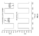
- FIG. 6 shows simulation results for the scenario where the laser DC bias current for transmission operations is 7 mA, the laser DC bias current for reception operations is 5.1 mA, the slope efficiency (VCSEL) is 0.06 mW/mA, and the photodiode responsivity is 0.16 A/W.
- a DC optical power of 0.43 mW generates an output DC bias current of ⁇ 70 ⁇ A at the output of the photodiode.
- a DC optical power of 0.31 mW generates a DC bias current of ⁇ 50 ⁇ A at the output of the photodiode.
- FIG. 7 shows measurement results for another scenario where the laser DC bias current for transmission operations is 9 mA, and the laser DC bias current for reception operations is 6 mA.
- controlling the DC bias used for reception operations relative to the DC bias used for transmission operations represents an effective way to control a switch to selectively connect an antenna port 212 to either a transmission port 214 or a reception port 216 .
- the solution presented herein uses an antenna switch 210 , which may be implemented on-chip, to selectively connect the transmission and reception paths to an antenna 400 , which removes the need for a bulky off-chip circulator. Further, because the DC bias current of a transmission signal is used to control the antenna switch 210 , the solution presented herein avoids the need for additional optical components (e.g., lasers, photodetectors, fibers, multiplexers, demultiplexers, etc.) in the central node 100 and/or the remote node 200 . Thus, the solution presented herein provides a smaller, cheaper, and less complex solution for isolating the transmission and reception chains than typically provided by past solutions.
- additional optical components e.g., lasers, photodetectors, fibers, multiplexers, demultiplexers, etc.
Abstract
Description
Δ(min)>I RF(max)[Z eff //Z ext ]A filter, (1)
where IRF(max) represents the maximum amplitude of the RF transmission signal, Zeff represents the effective RF input impedance of the transmission circuit path 230 (e.g., the impedance of the amplifier), Zext represents the RF input impedance of the
Δ(min)>V os +I RF(max)[Z eff //Z ext ]A filter, (2)
where Vos represents the comparator offset voltage.
Claims (15)
Priority Applications (2)
| Application Number | Priority Date | Filing Date | Title |
|---|---|---|---|
| US14/881,212 US9647752B2 (en) | 2015-10-13 | 2015-10-13 | Antenna switch control method for analog radio over fiber systems |
| PCT/EP2016/074269 WO2017064024A1 (en) | 2015-10-13 | 2016-10-11 | Antenna switch control method for analog radio over fiber systems |
Applications Claiming Priority (1)
| Application Number | Priority Date | Filing Date | Title |
|---|---|---|---|
| US14/881,212 US9647752B2 (en) | 2015-10-13 | 2015-10-13 | Antenna switch control method for analog radio over fiber systems |
Publications (2)
| Publication Number | Publication Date |
|---|---|
| US20170104524A1 US20170104524A1 (en) | 2017-04-13 |
| US9647752B2 true US9647752B2 (en) | 2017-05-09 |
Family
ID=57136860
Family Applications (1)
| Application Number | Title | Priority Date | Filing Date |
|---|---|---|---|
| US14/881,212 Expired - Fee Related US9647752B2 (en) | 2015-10-13 | 2015-10-13 | Antenna switch control method for analog radio over fiber systems |
Country Status (2)
| Country | Link |
|---|---|
| US (1) | US9647752B2 (en) |
| WO (1) | WO2017064024A1 (en) |
Families Citing this family (1)
| Publication number | Priority date | Publication date | Assignee | Title |
|---|---|---|---|---|
| CN113314846B (en) * | 2021-05-31 | 2022-04-05 | 西安电子科技大学 | High-power reconfigurable short-wave antenna based on light energy-carrying control |
Citations (10)
| Publication number | Priority date | Publication date | Assignee | Title |
|---|---|---|---|---|
| US6122083A (en) | 1994-03-18 | 2000-09-19 | Fujitsu Limited | Mobile communication system having a small base station and equipment for its system |
| US20030228151A1 (en) * | 2002-06-10 | 2003-12-11 | Tsutomu Niiho | Optical transmission device and optical transmission method for transmitting a burst radio signal |
| JP2004241909A (en) | 2003-02-04 | 2004-08-26 | Matsushita Electric Ind Co Ltd | System and device for wireless communication, and communication signal processor |
| US20060063494A1 (en) | 2004-10-04 | 2006-03-23 | Xiangdon Zhang | Remote front-end for a multi-antenna station |
| US20070092262A1 (en) * | 2005-10-25 | 2007-04-26 | Donald Bozarth | Adaptive optical transmitter for use with externally modulated lasers |
| US20070237181A1 (en) | 2004-07-29 | 2007-10-11 | Woungsik Cho | Method and System for Generating Switching Timing Signal for Separating Transmitting and Receiving Signal in Optical Repeater of Mobile Telecommunication Network Using Tdd and Ofdm Modulation |
| US20080056167A1 (en) | 2006-08-31 | 2008-03-06 | Sang-Ho Kim | Radio over fiber system and method for controlling transmission time |
| US20080145061A1 (en) | 2006-12-13 | 2008-06-19 | Han-Lim Lee | Radio over fiber link apparatus of time division duplex scheme |
| US20080260388A1 (en) | 2007-04-18 | 2008-10-23 | Sang-Ho Kim | Time division duplexing remote station having low-noise amplifier shared for uplink and downlink operations and wired relay method using the same |
| US20160182120A1 (en) * | 2010-11-18 | 2016-06-23 | Intel Corporation | Integrated transmit/receive switch |
-
2015
- 2015-10-13 US US14/881,212 patent/US9647752B2/en not_active Expired - Fee Related
-
2016
- 2016-10-11 WO PCT/EP2016/074269 patent/WO2017064024A1/en active Application Filing
Patent Citations (11)
| Publication number | Priority date | Publication date | Assignee | Title |
|---|---|---|---|---|
| US6122083A (en) | 1994-03-18 | 2000-09-19 | Fujitsu Limited | Mobile communication system having a small base station and equipment for its system |
| US20030228151A1 (en) * | 2002-06-10 | 2003-12-11 | Tsutomu Niiho | Optical transmission device and optical transmission method for transmitting a burst radio signal |
| EP1372274A2 (en) | 2002-06-10 | 2003-12-17 | Matsushita Electric Industrial Co., Ltd. | Optical transmission device and optical transmission method for transmitting a burst radio signal |
| JP2004241909A (en) | 2003-02-04 | 2004-08-26 | Matsushita Electric Ind Co Ltd | System and device for wireless communication, and communication signal processor |
| US20070237181A1 (en) | 2004-07-29 | 2007-10-11 | Woungsik Cho | Method and System for Generating Switching Timing Signal for Separating Transmitting and Receiving Signal in Optical Repeater of Mobile Telecommunication Network Using Tdd and Ofdm Modulation |
| US20060063494A1 (en) | 2004-10-04 | 2006-03-23 | Xiangdon Zhang | Remote front-end for a multi-antenna station |
| US20070092262A1 (en) * | 2005-10-25 | 2007-04-26 | Donald Bozarth | Adaptive optical transmitter for use with externally modulated lasers |
| US20080056167A1 (en) | 2006-08-31 | 2008-03-06 | Sang-Ho Kim | Radio over fiber system and method for controlling transmission time |
| US20080145061A1 (en) | 2006-12-13 | 2008-06-19 | Han-Lim Lee | Radio over fiber link apparatus of time division duplex scheme |
| US20080260388A1 (en) | 2007-04-18 | 2008-10-23 | Sang-Ho Kim | Time division duplexing remote station having low-noise amplifier shared for uplink and downlink operations and wired relay method using the same |
| US20160182120A1 (en) * | 2010-11-18 | 2016-06-23 | Intel Corporation | Integrated transmit/receive switch |
Also Published As
| Publication number | Publication date |
|---|---|
| US20170104524A1 (en) | 2017-04-13 |
| WO2017064024A1 (en) | 2017-04-20 |
Similar Documents
| Publication | Publication Date | Title |
|---|---|---|
| US10003410B2 (en) | Optical receiver, optical termination device, and optical communication system | |
| US10056998B2 (en) | Switching sub-system for distributed antenna systems using time division duplexing | |
| US10044328B2 (en) | Transimpedance amplifier with bandwidth extender | |
| CN108173598B (en) | Optical receiver and optical communication method | |
| EP1400013B1 (en) | Method and apparatus for a transceiver having a constant power output | |
| US9496826B2 (en) | Transimpedance amplifier | |
| US7304543B2 (en) | Burst-mode TIA (trans-impedance amplifier) | |
| CN103312364A (en) | Radio frequency modules | |
| JP5811955B2 (en) | Burst signal receiving apparatus and method, PON station apparatus, PON system | |
| KR20160060127A (en) | Trans-impedance amplifier circuit | |
| EP2634941A1 (en) | Method and device for determining whether a configuration of an optical transmission interface has to be adjusted | |
| US9647752B2 (en) | Antenna switch control method for analog radio over fiber systems | |
| CN110785949B (en) | Optical receiver | |
| US20180294889A1 (en) | Optical receiver and method of controlling optical receiver | |
| JP2009253598A (en) | Phase-modulated signal receiving device | |
| CN109495182B (en) | Receiving end calibration method and device of coherent optical module | |
| CN111567003B (en) | Method and device for determining a signal modulation type, and arrangement of an amplifying unit | |
| KR101539196B1 (en) | Method and Device for Receiving in Coherent Optical Communication System | |
| US11444717B2 (en) | Multi-band optical network interface | |
| EP3614582A1 (en) | Multiplexed integrating amplifier for loss of signal detection | |
| US9401761B2 (en) | Method and device for determining whether a configuration of an optical transmission interface has to be adjusted | |
| JP5449606B1 (en) | Optical receiver and optical communication system | |
| CN109474350B (en) | Optical module | |
| EP3678382B1 (en) | Method and device for amplifying uplink light of passive optical network | |
| US10903973B2 (en) | Distributed antenna system for time division duplex |
Legal Events
| Date | Code | Title | Description |
|---|---|---|---|
| AS | Assignment |
Owner name: TELEFONAKTIEBOLAGET L M ERICSSON (PUBL), SWEDEN Free format text: ASSIGNMENT OF ASSIGNORS INTEREST;ASSIGNORS:AHMAD, WAQAS;SJOELAND, HENRIK;REEL/FRAME:037044/0767 Effective date: 20151008 |
|
| AS | Assignment |
Owner name: TELEFONAKTIEBOLAGET LM ERICSSON (PUBL), SWEDEN Free format text: CHANGE OF NAME;ASSIGNOR:TELEFONAKTIEBOLAGET L M ERICSSON (PUBL);REEL/FRAME:041778/0262 Effective date: 20151119 |
|
| STCF | Information on status: patent grant |
Free format text: PATENTED CASE |
|
| FEPP | Fee payment procedure |
Free format text: MAINTENANCE FEE REMINDER MAILED (ORIGINAL EVENT CODE: REM.); ENTITY STATUS OF PATENT OWNER: LARGE ENTITY |
|
| LAPS | Lapse for failure to pay maintenance fees |
Free format text: PATENT EXPIRED FOR FAILURE TO PAY MAINTENANCE FEES (ORIGINAL EVENT CODE: EXP.); ENTITY STATUS OF PATENT OWNER: LARGE ENTITY |
|
| STCH | Information on status: patent discontinuation |
Free format text: PATENT EXPIRED DUE TO NONPAYMENT OF MAINTENANCE FEES UNDER 37 CFR 1.362 |
|
| FP | Lapsed due to failure to pay maintenance fee |
Effective date: 20210509 |