US9635232B2 - Camera module having MEMS actuator, connecting method for shutter coil of camera module and camera module manufactured by the same method - Google Patents
Camera module having MEMS actuator, connecting method for shutter coil of camera module and camera module manufactured by the same method Download PDFInfo
- Publication number
- US9635232B2 US9635232B2 US14/599,244 US201514599244A US9635232B2 US 9635232 B2 US9635232 B2 US 9635232B2 US 201514599244 A US201514599244 A US 201514599244A US 9635232 B2 US9635232 B2 US 9635232B2
- Authority
- US
- United States
- Prior art keywords
- camera module
- substrate
- conductive pattern
- pattern
- housing
- Prior art date
- Legal status (The legal status is an assumption and is not a legal conclusion. Google has not performed a legal analysis and makes no representation as to the accuracy of the status listed.)
- Active
Links
Images


Classifications
-
- H04N5/2257—
-
- H—ELECTRICITY
- H04—ELECTRIC COMMUNICATION TECHNIQUE
- H04N—PICTORIAL COMMUNICATION, e.g. TELEVISION
- H04N23/00—Cameras or camera modules comprising electronic image sensors; Control thereof
- H04N23/57—Mechanical or electrical details of cameras or camera modules specially adapted for being embedded in other devices
-
- G—PHYSICS
- G02—OPTICS
- G02B—OPTICAL ELEMENTS, SYSTEMS OR APPARATUS
- G02B7/00—Mountings, adjusting means, or light-tight connections, for optical elements
- G02B7/02—Mountings, adjusting means, or light-tight connections, for optical elements for lenses
- G02B7/04—Mountings, adjusting means, or light-tight connections, for optical elements for lenses with mechanism for focusing or varying magnification
- G02B7/08—Mountings, adjusting means, or light-tight connections, for optical elements for lenses with mechanism for focusing or varying magnification adapted to co-operate with a remote control mechanism
-
- B—PERFORMING OPERATIONS; TRANSPORTING
- B81—MICROSTRUCTURAL TECHNOLOGY
- B81B—MICROSTRUCTURAL DEVICES OR SYSTEMS, e.g. MICROMECHANICAL DEVICES
- B81B7/00—Microstructural systems; Auxiliary parts of microstructural devices or systems
- B81B7/0006—Interconnects
-
- B—PERFORMING OPERATIONS; TRANSPORTING
- B81—MICROSTRUCTURAL TECHNOLOGY
- B81B—MICROSTRUCTURAL DEVICES OR SYSTEMS, e.g. MICROMECHANICAL DEVICES
- B81B7/00—Microstructural systems; Auxiliary parts of microstructural devices or systems
- B81B7/0032—Packages or encapsulation
- B81B7/007—Interconnections between the MEMS and external electrical signals
-
- B—PERFORMING OPERATIONS; TRANSPORTING
- B81—MICROSTRUCTURAL TECHNOLOGY
- B81B—MICROSTRUCTURAL DEVICES OR SYSTEMS, e.g. MICROMECHANICAL DEVICES
- B81B7/00—Microstructural systems; Auxiliary parts of microstructural devices or systems
- B81B7/02—Microstructural systems; Auxiliary parts of microstructural devices or systems containing distinct electrical or optical devices of particular relevance for their function, e.g. microelectro-mechanical systems [MEMS]
-
- G—PHYSICS
- G03—PHOTOGRAPHY; CINEMATOGRAPHY; ANALOGOUS TECHNIQUES USING WAVES OTHER THAN OPTICAL WAVES; ELECTROGRAPHY; HOLOGRAPHY
- G03B—APPARATUS OR ARRANGEMENTS FOR TAKING PHOTOGRAPHS OR FOR PROJECTING OR VIEWING THEM; APPARATUS OR ARRANGEMENTS EMPLOYING ANALOGOUS TECHNIQUES USING WAVES OTHER THAN OPTICAL WAVES; ACCESSORIES THEREFOR
- G03B3/00—Focusing arrangements of general interest for cameras, projectors or printers
- G03B3/10—Power-operated focusing
-
- G—PHYSICS
- G03—PHOTOGRAPHY; CINEMATOGRAPHY; ANALOGOUS TECHNIQUES USING WAVES OTHER THAN OPTICAL WAVES; ELECTROGRAPHY; HOLOGRAPHY
- G03B—APPARATUS OR ARRANGEMENTS FOR TAKING PHOTOGRAPHS OR FOR PROJECTING OR VIEWING THEM; APPARATUS OR ARRANGEMENTS EMPLOYING ANALOGOUS TECHNIQUES USING WAVES OTHER THAN OPTICAL WAVES; ACCESSORIES THEREFOR
- G03B9/00—Exposure-making shutters; Diaphragms
- G03B9/08—Shutters
-
- H—ELECTRICITY
- H04—ELECTRIC COMMUNICATION TECHNIQUE
- H04N—PICTORIAL COMMUNICATION, e.g. TELEVISION
- H04N23/00—Cameras or camera modules comprising electronic image sensors; Control thereof
- H04N23/50—Constructional details
- H04N23/54—Mounting of pick-up tubes, electronic image sensors, deviation or focusing coils
-
- H—ELECTRICITY
- H04—ELECTRIC COMMUNICATION TECHNIQUE
- H04N—PICTORIAL COMMUNICATION, e.g. TELEVISION
- H04N23/00—Cameras or camera modules comprising electronic image sensors; Control thereof
- H04N23/50—Constructional details
- H04N23/55—Optical parts specially adapted for electronic image sensors; Mounting thereof
-
- H04N5/2253—
-
- H04N5/2254—
-
- G—PHYSICS
- G03—PHOTOGRAPHY; CINEMATOGRAPHY; ANALOGOUS TECHNIQUES USING WAVES OTHER THAN OPTICAL WAVES; ELECTROGRAPHY; HOLOGRAPHY
- G03B—APPARATUS OR ARRANGEMENTS FOR TAKING PHOTOGRAPHS OR FOR PROJECTING OR VIEWING THEM; APPARATUS OR ARRANGEMENTS EMPLOYING ANALOGOUS TECHNIQUES USING WAVES OTHER THAN OPTICAL WAVES; ACCESSORIES THEREFOR
- G03B2205/00—Adjustment of optical system relative to image or object surface other than for focusing
- G03B2205/0053—Driving means for the movement of one or more optical element
- G03B2205/0084—Driving means for the movement of one or more optical element using other types of actuators
Definitions
- the present invention relates to a camera module, and particularly to a camera module which can facilely form an electrical connection between an MEMS (Micro Electro Mechanical Systems) actuator and an electrode pad of a substrate, a connecting method for a shutter coil of the camera module, which can easily form a connection between the shutter coil and an output terminal pad of a PCB (Printed Circuit Board) through welding, and a camera module manufactured by using the same method.
- MEMS Micro Electro Mechanical Systems
- PCB Print Circuit Board
- a compact camera module is being applied to various IT equipment and mobile communication devices such as a camera phone, a PDA and a smart phone.
- the camera module includes an image sensor such as CCD and CMOS as a main component, and it is so manufactured as to be capable of adjusting focus, thereby controlling an image size.
- an image sensor such as CCD and CMOS as a main component
- the camera module includes a plurality of lenses, and each lens is movably arranged so that a relative distance can be changed to control a focal distance.
- a moving lens is fixed to a silicon wafer instead of the existing VCM. Therefore, when a voltage is applied, a portion to which the moving lens is fixed is move up and down by electrostatic force to minutely adjust the moving lens, thereby performing an auto-focusing function.
- an electrode terminal 11 of the MEMS actuator 10 and an electrode pad 21 of a substrate are soldered with an FPCB (Flexible Print Circuit Board) 30 so as to be electrically connected with each other.
- FPCB Flexible Print Circuit Board
- the electrode terminal is structurally formed at a lower surface the problems are that it takes much time to solder the PCB to the electrode terminal and also troubles occurs frequently after the electrical connection.
- the camera module may be defective due to high temperature and thermal shock during the soldering.
- a camera has a shutter which functions to control time for transferring light through a lens to an image sensor.
- the shutter is opened only for a predetermined time period to allow light to pass and then closed after the predetermined time period to block out the light.
- the shutter takes the shape of a coil to obtain magnetic field and electromagnetic force for driving the shutter.
- An object of the present invention is to provide a camera module which can facilely form an electrical connection between an electrode terminal of an MEMS actuator and an electrode pad of a substrate,
- another object of the present invention is to a camera module in which a shutter coil is connected with an output terminal pad by welding, thereby protecting other components of the camera module from heat and also preventing performance deterioration of an image sensor and the like.
- the present invention provides a camera module including a substrate which is provided with an electrode pad and an image sensor; a housing Which is stacked on the substrate and of which an upper portion is opened so that light is incident to the image sensor; a MEMS actuator which is installed at the housing and has an electrode terminal at one side thereof, and a conductive pattern which is formed at the housing, wherein a lower end of the conductive pattern is connected with the electrode pad of the substrate, and an upper end thereof is connected with the electrode terminal of the MEMS actuator.
- a lower end of the conductive pattern is exposed through a bottom surface of the housing so as to be connected with the electrode pad of the substrate, and an upper end of the conductive pattern is exposed through an upper surface of the housing so as to be connected with the electrode terminal of the MEMS actuator.
- the electrode pad of the substrate comprises a plurality of positive terminals and negative terminals, and a lower end of the conductive pattern is connected with the plurality of positive terminals and negative terminals.
- the housing includes a holder which forms a light running space through light is incident to the image sensor, and a lens barrel which is inserted into the light running space of the holder and formed with a hole so as to fix one or more lenses.
- the conductive pattern includes a first conductive pattern and a second conductive pattern
- the first conductive pattern is formed to be extended from the electrode pad to an inner surface of the light running space of the holder
- the second conductive pattern is formed at an outer surface of the lens barrel so as to be contacted with the first conductive pattern and also to be extended to an upper surface.
- an extended portion is formed at an upper end of the lens barrel so as to be contacted with the electrode terminal of the MEMS actuator, and the second conductive pattern is extended to an upper surface of the extended portion.
- the present invention provides a shutter coil connection method of the camera module, which has a shutter and a MEMS actuator for performing auto-focus, including welding a shutter coil extended from the shutter to an output terminal pad formed at a PCB so as to transfer a control signal of the shutter.
- the shutter coil and the output terminal pad are respectively provided in a pair so as to be corresponding to a positive pole and a negative pole.
- the shutter coil is welded by a welding machine.
- the shutter coil has a diameter of 0.04 ⁇ 0.06 mm, and a voltage at a welding tip of the welding machine is 1.2 ⁇ 1.4V, and welding time of the welding machine is 5 ⁇ 9 ms.
- connection without the PCB, thereby enhancing price competitiveness.
- the shutter coil is connected with the output terminal pad by welding, it is possible to protect other components of the camera module from heat and also prevent the performance deterioration of the image sensor and the like.
- FIG. 1 is a perspective view of a conventional camera module.
- FIG. 2 is an exploded perspective view of a camera module according to an embodiment of the present invention.
- FIG. 3 a is a plan view of camera module housing according to the embodiment of the present invention.
- FIG. 3 b is a side view of the camera module housing according to the embodiment of the present invention.
- FIG. 3 c is a bottom view of the camera module housing according to the embodiment of the present invention.
- FIG. 4 is a perspective view of a lens barrel of the camera module according to the embodiment of the present invention.
- FIG. 5 is an enlarged view of the lens barrel according to the embodiment of the present invention.
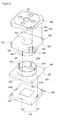
- FIG. 6 is an exploded perspective view of a camera module according to another embodiment of the present invention.
- FIG. 7 is an exploded perspective view of the camera module including an MEMS actuator and a shutter.
- FIG. 8 is a flow chart showing a connection method of a shutter coil of the camera module according to an embodiment of the present invention.
- FIGS. 9 to 12 are photographs showing a connecting process in the connection method of a shutter coil of the camera module according to the embodiment of the present invention.
- the expression that “the certain construction element is directly connected to the construction element” means that the third construction element is not interposed therebetween.
- the camera module includes a substrate 100 in which an electrode pad 110 and an image sensor 120 are formed, an housing 200 , 300 which is stacked on the substrate 100 and of which an upper portion is opened so that light is incident to the image sensor 120 , an MEMs actuator 400 which is installed at the housing 200 , 300 and has an electrode terminal 420 at one side thereof, and a conductive pattern which is formed at the housing 200 , 300 .
- a lower end of the conductive pattern is connected with the electrode pad 110 , and an upper end thereof is connected with the electrode terminal 420 of the MEMS actuator 400 .
- the conductive pattern can be formed by all general methods of forming a conductive material, and also can be patterned at the same time of injection molding of the housing.
- a general PCB can be used as the substrate 100 .
- an electric wiring At an upper surface of the substrate 100 , there is formed an electric wiring.
- a positive terminal 111 and a negative terminal 112 are formed at a side surface of the substrate 100 , and also another positive terminal 111 a and another negative terminal 112 a may be formed at an opposite side surface thereof.
- the image sensor 120 may include a pixel area (not shown) having a plurality of pixels, and a plurality of electrodes (not shown).
- the pluralities of electrodes are electrically connected with electrodes (not shown) of the substrate 100 by using a wire bonding equipment.
- the housing 200 , 300 may have any structure, if it can be stacked on the substrate 100 , and its upper portion is opened so that light is incident to the image sensor 120 , and the MEMS actuator 400 can be fixed thereon.
- the housing has a structure that a holder 200 and a lens barrel 300 are coupled with each other.
- the holder 200 is formed at the substrate 100 so as to form a light miming space 211 which is opened so that light is incident to the image sensor 120 .
- an upper portion of the light running space 211 may be formed into a cylindrical opening so as to receive the lens barrel 300 , and a lower portion thereof may be formed into a square opening so that light is incident to the image sensor 120 . Therefore, an upper portion 210 of the holder 200 is formed into a cylindrical shape, and a lower portion 220 thereof is formed into a square shape.
- the holder 200 may have any structure or shape, if it can form the light running space 211 .
- a first conductive pattern 231 , 232 is formed at an inner side surface of the light running space 211 .
- the first conductive pattern 231 , 232 will be described in detail with reference to FIGS. 3 a to 3 c.
- the first conductive pattern 231 , 232 is formed at the inner side surface of the light running space 211 so as to have a desired thickness and width. Further as shown in FIG. 3 c , the first conductive pattern 231 , 232 is exposed through a side surface of a bottom surface 221 of the holder 200 so as to be electrically connected with the electrode pad 110 when the holder 200 is stacked on the substrate 100 of FIG. 2 .
- the first conductive pattern 231 , 232 exposed through the bottom surface 221 of the holder 200 is bonded so as to be electrically connected by using a conductive adhesive such as Ag-epoxy.
- the electrode pad 110 of the substrate 100 is provided in plural number 111 a , 112 a , another conductive pattern 231 a , 232 a which is not described is electrically connected with them.
- the lens barrel 300 is disposed at the upper portion of the holder 200 , and a circular hole 232 is formed at a center portion of the lens barrel 300 so as to open the lens barrel 300 up and down.
- a fixed lens (not shown) is inserted into the circular hole 232 , and a second conductive pattern 330 , 340 is formed at an outer surface of the lens barrel 300 .
- the lens barrel 300 has a desired size and shape which can be inserted into the light running space 211 .
- the second conductive pattern 330 , 340 includes a lower end 332 , 342 , an upper end 334 , 344 , and a connection wire 331 , 341 which electrically connects the lower end 332 , 342 and the upper end 334 , 344 .
- the lower end 332 , 342 of the second conductive pattern 330 , 340 is formed at an outer surface of the lower end 310 of the lens barrel 300 in a height direction thereof so as to be electrically connected with the first conductive pattern 231 , 232 of the holder 200 by contacting each other.
- Another lower end 333 , 343 of the second conductive pattern 330 , 340 may be additionally formed according to the number of the electrode pads 110 formed at the substrate 100 . If one of the conductive patterns is defective, the electrical connection can be maintained by using other conductive patterns, thereby increasing electrical reliability thereof.
- An upper portion 320 of the lens barrel 300 is formed into a plate shape, and protrusions 321 are formed at a side surface thereof so as to fix the MEMS actuator 400 .
- One of the protrusions 321 is protruded upward in a desired height so as to form an extended portion 322 .
- the upper end 334 , 344 of the second conductive pattern 330 , 340 is formed at an upper surface 322 a of the extended portion 322 ,
- the extended portion 322 has a desired height which can be contacted with the electrode terminal 420 of the MEMS actuator 400 when the MEMS actuator 400 is installed at the lens barrel 300 .
- the MEMS actuator minutely adjusts a moving lens (not Shown) using a silicon wafer instead of an existing voice coil, and the electrode terminal 420 is formed at an upper surface thereof.
- An opening 412 is formed at a center portion of the MEMS actuator 400 .
- a lens mount pad (not shown) for supporting the moving lens (not shown) is formed at a side surface of the opening 412 .
- the lens mount pad is driven up and down by electrostatic force so as to adjust focus of the moving lens.
- the electrode terminal 420 of the MEMS actuator 400 includes a positive electrode 421 and a negative electrode 422 which are electrically connected by being contacted with.
- the electrode terminal 420 and the upper end 334 , 344 of the second conductive pattern 330 , 340 may be fixed to each other using a conductive adhesive.
- the conductive adhesive is an anisotropic conductive adhesive.
- the electrode pad 110 of the substrate 100 and the electrode terminal 420 of the MEMS actuator 400 are connected with other through the first and second conductive patterns 231 , 232 , 330 , 340 so as to be electrically connected at the same time of assembling the camera module, thereby simplifying a manufacturing process thereof.
- FIG. 6 shows an exploded perspective view of a camera module according to another embodiment of the present invention.
- the positive terminal 111 and the negative terminal of the electrode pad 110 are formed at one side of the substrate 100 so as to be electrically connected with the first conductive pattern 231 , 232 .
- first conductive pattern 231 , 232 is electrically connected with the second conductive pattern 330 , 340 of the lens barrel 300 , and the second conductive pattern 330 , 340 is connected with the electrode terminal 410 of the MEMS actuator 400 .
- the electrode pad 110 formed at the substrate 100 can be facilely connected with the electrode terminal 420 of the MEMS actuator 400 .
- the electrode pad 110 does not need to change its existing position, and an extra manufacturing cost is not needed.
- FIG. 7 is an exploded perspective view of the camera module including an MEMS actuator and a shutter.
- the camera module manufactured by a shutter coil connection method according to the present invention includes an MEMS actuator 20 and a shutter 30 in order to reduce its weight and size.
- the camera module may include an electromagnetic shielding box 10 , an image sensor 40 and a PCB 50 .
- a comb driver functions to adjust the focus using electrostatic force and the shutter 30 is operated at a predetermined speed by magnetic field and electromagnetic force based on a shutter coil wound on a magnetic body.
- the image sensor 40 functions to receive an optical signal from an outside and convert it into an electric signal
- the PCB 50 is a ceramic substrate on which a circuit for transferring various electric signals is printed.
- the image sensor 40 , the electromagnetic shielding box 10 and the like are may be mounted on an upper pad of the PCB 50 .
- FIG. 8 is a flow chart showing a connection method of a shutter coil of the camera module according to an embodiment of the present invention.
- the shutter coil 32 , 34 extended from the shutter 30 is welded to an output terminal pad 52 , 54 formed at the PCB 50 in order to transfer a control signal of the shutter 30 (S 10 ).
- the shutter coil 32 , 34 is a wire which is extended from the coil wound on the magnetic body of the shutter 30 to an outside.
- the shutter coil 32 , 34 is formed of copper.
- the output terminal pad 52 , 54 of the PCB 50 is provided in a pair so as to be welded with the shutter coil 32 , 34 having a positive pole and a negative pole.
- the output terminal pad 52 , 54 is formed by gold-plating on a copper foil.
- the shutter coil 32 , 34 is welded by a welding machine W.
- a voltage at a welding tip of the welding machine W is 1.2 ⁇ 1.4V and welding time of the welding machine W is 5 ⁇ 9 ms.
- the heat since heat is generated locally, the heat does not have any influence on other elements (e.g., the image sensor or the MEMS actuator).
- FIGS. 9 to 12 are photographs showing a connecting process in the connection method of a shutter coil of the camera module according to the embodiment of the present invention.
- each shutter coil 32 , 34 is welded to the output terminal pad 52 , 54 so as to be corresponding to a positive pole and a negative pole suing the welding machine W.
- the output terminal pad 52 , 54 and the shutter coil 32 , 34 are directly coupled with each other using the heat which is locally generated at a contacted point therebetween by a potential difference of the welding tip without a solder,
- connection is not achieved by a solder, it is not necessary to provide a space for other material (e.g., solder, Ag-epoxy), and also it is facile to mount the electromagnetic shielding box 10 .
- connection without the PCB, thereby enhancing price competitiveness.
- the shutter coil is connected with the output terminal pad by welding, it is possible to protect other components of the camera module from heat and also prevent the performance deterioration of the image sensor and the like.
Abstract
Disclosed is a camera module including a substrate which is provided with an electrode pad and an image sensor; a housing which is stacked on the substrate and of which an upper portion is opened so that light is incident to the image sensor; a MEMS actuator which is installed at the housing and has an electrode terminal at one side thereof, and a conductive pattern which is formed at the housing, wherein a lower end of the conductive pattern is connected with the electrode pad of the substrate, and an upper end thereof is connected with the electrode terminal of the MEMS actuator, whereby it is possible to improve electrical reliability between the electrode terminal of the MEMS actuator and the electrode pad of the substrate and facilely form the electrical connection therebetween, thereby reducing the number of processes.
Description
This application is a Continuation of co-pending U.S. application Ser. No. 13/698,218 filed on Nov. 15, 2012, which is the National Phase of PCI International Application No. PCT/KR2011/003728 filed on May 20, 2011, which claims priority to Patent Application No. 10-2010-0047444 filed in the Republic of Korea on May 20, 2010, and Patent Application No 10-2010-0098431 filed in the Republic of Korea on Oct. 8, 2010. The entire content of all of the above applications are hereby expressly incorporated by reference.
The present invention relates to a camera module, and particularly to a camera module which can facilely form an electrical connection between an MEMS (Micro Electro Mechanical Systems) actuator and an electrode pad of a substrate, a connecting method for a shutter coil of the camera module, which can easily form a connection between the shutter coil and an output terminal pad of a PCB (Printed Circuit Board) through welding, and a camera module manufactured by using the same method.
Generally, a compact camera module is being applied to various IT equipment and mobile communication devices such as a camera phone, a PDA and a smart phone.
The camera module includes an image sensor such as CCD and CMOS as a main component, and it is so manufactured as to be capable of adjusting focus, thereby controlling an image size.
Herein, the camera module includes a plurality of lenses, and each lens is movably arranged so that a relative distance can be changed to control a focal distance.
Recently, a study on realizing auto-focus using an MEMS actuator instead of an existing VCM (Voice Coil Motor) has been actively carried out.
In the MEMS actuator, a moving lens is fixed to a silicon wafer instead of the existing VCM. Therefore, when a voltage is applied, a portion to which the moving lens is fixed is move up and down by electrostatic force to minutely adjust the moving lens, thereby performing an auto-focusing function.
As shown in FIG. 1 , an electrode terminal 11 of the MEMS actuator 10 and an electrode pad 21 of a substrate are soldered with an FPCB (Flexible Print Circuit Board) 30 so as to be electrically connected with each other.
However, in the MEMS actuator, since the electrode terminal is structurally formed at a lower surface the problems are that it takes much time to solder the PCB to the electrode terminal and also troubles occurs frequently after the electrical connection.
Further, the camera module may be defective due to high temperature and thermal shock during the soldering.
Meanwhile, a camera has a shutter which functions to control time for transferring light through a lens to an image sensor. The shutter is opened only for a predetermined time period to allow light to pass and then closed after the predetermined time period to block out the light. The shutter takes the shape of a coil to obtain magnetic field and electromagnetic force for driving the shutter.
In order to connect a coil wire terminal of the shutter and positive and negative pads of a substrate which can perform a command of a driver IC, a manual soldering method and a method of coating and hardening conductive Ag-epoxy resin are main used. However, these methods have some problems in workability and productivity, and also any connection method applied to a very small space such as a camera module always has various problems.
There are some representative problems in that a terminal of snubber circuit of the sensitive MEMS actuator is weak in heat, flux gas of lead generated upon soldering has bad influence on an image sensor and an IR filter, thereby deteriorating an image quality, and a short-circuit with respect to a peripheral terminal such as a grounding portion may be generated, thereby causing a trouble in the operation of the shutter.
An object of the present invention is to provide a camera module which can facilely form an electrical connection between an electrode terminal of an MEMS actuator and an electrode pad of a substrate,
Further, another object of the present invention is to a camera module in which a shutter coil is connected with an output terminal pad by welding, thereby protecting other components of the camera module from heat and also preventing performance deterioration of an image sensor and the like.
To achieve the object of the present invention, the present invention provides a camera module including a substrate which is provided with an electrode pad and an image sensor; a housing Which is stacked on the substrate and of which an upper portion is opened so that light is incident to the image sensor; a MEMS actuator which is installed at the housing and has an electrode terminal at one side thereof, and a conductive pattern which is formed at the housing, wherein a lower end of the conductive pattern is connected with the electrode pad of the substrate, and an upper end thereof is connected with the electrode terminal of the MEMS actuator.
Preferably, a lower end of the conductive pattern is exposed through a bottom surface of the housing so as to be connected with the electrode pad of the substrate, and an upper end of the conductive pattern is exposed through an upper surface of the housing so as to be connected with the electrode terminal of the MEMS actuator.
Preferably, the electrode pad of the substrate comprises a plurality of positive terminals and negative terminals, and a lower end of the conductive pattern is connected with the plurality of positive terminals and negative terminals.
Preferably, the housing includes a holder which forms a light running space through light is incident to the image sensor, and a lens barrel which is inserted into the light running space of the holder and formed with a hole so as to fix one or more lenses.
Preferably, the conductive pattern includes a first conductive pattern and a second conductive pattern, and the first conductive pattern is formed to be extended from the electrode pad to an inner surface of the light running space of the holder, and the second conductive pattern is formed at an outer surface of the lens barrel so as to be contacted with the first conductive pattern and also to be extended to an upper surface.
Preferably, an extended portion is formed at an upper end of the lens barrel so as to be contacted with the electrode terminal of the MEMS actuator, and the second conductive pattern is extended to an upper surface of the extended portion.
Further, the present invention provides a shutter coil connection method of the camera module, which has a shutter and a MEMS actuator for performing auto-focus, including welding a shutter coil extended from the shutter to an output terminal pad formed at a PCB so as to transfer a control signal of the shutter.
Preferably, wherein the shutter coil and the output terminal pad are respectively provided in a pair so as to be corresponding to a positive pole and a negative pole.
Preferably, the shutter coil is welded by a welding machine.
Preferably, the shutter coil has a diameter of 0.04˜0.06 mm, and a voltage at a welding tip of the welding machine is 1.2˜1.4V, and welding time of the welding machine is 5˜9 ms.
According to the present invention as described above, it is possible to improve electrical reliability between the electrode terminal of the MEMS actuator and the electrode pad of the substrate and facilely form the electrical connection therebetween, thereby reducing the number of processes.
Further, it is additionally possible to form the connection without the PCB, thereby enhancing price competitiveness.
Furthermore, according to one embodiment of the present invention, since the shutter coil is connected with the output terminal pad by welding, it is possible to protect other components of the camera module from heat and also prevent the performance deterioration of the image sensor and the like.
*28 The above and other objects, features and advantages of the present invention will become apparent from the following description of preferred embodiments given in conjunction with the accompanying drawings, in which:
Hereinafter, the embodiments of the present invention will be described in detail with reference to accompanying drawings. However, the present invention is not limited to the embodiments, and it should be understood that the present invention comprises all of equivalents and substitutes included in the technical scope and spirit of the invention.
It is to be noted that, in this specification, the expression that “a certain construction element is connected to another construction element” means that the certain construction element is directly connected to the construction element, and also means that a third construction element may be interposed therebetween.
On the other hand, the expression that “the certain construction element is directly connected to the construction element” means that the third construction element is not interposed therebetween.
The terms used herein are merely to describe a specific embodiment, and thus the present invention is not limited to them. Further, as far as singular expression clearly denotes a different meaning in context, it includes plural expression.
It is understood that terms “comprises”, “comprising”, “includes” or “has” intend to indicate the existence of features, numerals, steps, operations, elements and components described in the specification or the existence of the combination of these, and do not exclude the existence of one or more other features, numerals, steps, operations, elements and components or the existence of the combination of these or additional possibility beforehand.
Also, it is understood that accompanying drawings are enlarged or reduced for the convenience of explanation.
The same reference numerals are given to the same or corresponding parts, and the description thereof will not be repeated.
Referring to FIG. 2 , the camera module according to an embodiment of the present invention includes a substrate 100 in which an electrode pad 110 and an image sensor 120 are formed, an housing 200, 300 which is stacked on the substrate 100 and of which an upper portion is opened so that light is incident to the image sensor 120, an MEMs actuator 400 which is installed at the housing 200, 300 and has an electrode terminal 420 at one side thereof, and a conductive pattern which is formed at the housing 200, 300. A lower end of the conductive pattern is connected with the electrode pad 110, and an upper end thereof is connected with the electrode terminal 420 of the MEMS actuator 400.
The conductive pattern can be formed by all general methods of forming a conductive material, and also can be patterned at the same time of injection molding of the housing.
A general PCB can be used as the substrate 100. At an upper surface of the substrate 100, there is formed an electric wiring.
In the electrode pad 110 of the substrate 100, a positive terminal 111 and a negative terminal 112 are formed at a side surface of the substrate 100, and also another positive terminal 111 a and another negative terminal 112 a may be formed at an opposite side surface thereof.
The image sensor 120 may include a pixel area (not shown) having a plurality of pixels, and a plurality of electrodes (not shown). Herein, the pluralities of electrodes are electrically connected with electrodes (not shown) of the substrate 100 by using a wire bonding equipment.
The housing 200, 300 may have any structure, if it can be stacked on the substrate 100, and its upper portion is opened so that light is incident to the image sensor 120, and the MEMS actuator 400 can be fixed thereon.
In the camera module according to the embodiment of the present invention, the housing has a structure that a holder 200 and a lens barrel 300 are coupled with each other.
The holder 200 is formed at the substrate 100 so as to form a light miming space 211 which is opened so that light is incident to the image sensor 120.
More detailed, an upper portion of the light running space 211 may be formed into a cylindrical opening so as to receive the lens barrel 300, and a lower portion thereof may be formed into a square opening so that light is incident to the image sensor 120. Therefore, an upper portion 210 of the holder 200 is formed into a cylindrical shape, and a lower portion 220 thereof is formed into a square shape.
However, the holder 200 may have any structure or shape, if it can form the light running space 211.
A first conductive pattern 231, 232 is formed at an inner side surface of the light running space 211. The first conductive pattern 231, 232 will be described in detail with reference to FIGS. 3a to 3 c.
As shown in FIGS. 3a and 3b , the first conductive pattern 231, 232 is formed at the inner side surface of the light running space 211 so as to have a desired thickness and width. Further as shown in FIG. 3c , the first conductive pattern 231, 232 is exposed through a side surface of a bottom surface 221 of the holder 200 so as to be electrically connected with the electrode pad 110 when the holder 200 is stacked on the substrate 100 of FIG. 2 .
Herein, the first conductive pattern 231, 232 exposed through the bottom surface 221 of the holder 200 is bonded so as to be electrically connected by using a conductive adhesive such as Ag-epoxy.
In case that the electrode pad 110 of the substrate 100 is provided in plural number 111 a, 112 a, another conductive pattern 231 a, 232 a which is not described is electrically connected with them.
The lens barrel 300 is disposed at the upper portion of the holder 200, and a circular hole 232 is formed at a center portion of the lens barrel 300 so as to open the lens barrel 300 up and down. A fixed lens (not shown) is inserted into the circular hole 232, and a second conductive pattern 330, 340 is formed at an outer surface of the lens barrel 300.
The lens barrel 300 has a desired size and shape which can be inserted into the light running space 211.
Referring to FIGS. 4 and 5 , the second conductive pattern 330, 340 includes a lower end 332, 342, an upper end 334, 344, and a connection wire 331, 341 which electrically connects the lower end 332, 342 and the upper end 334, 344.
The lower end 332, 342 of the second conductive pattern 330, 340 is formed at an outer surface of the lower end 310 of the lens barrel 300 in a height direction thereof so as to be electrically connected with the first conductive pattern 231, 232 of the holder 200 by contacting each other.
Another lower end 333, 343 of the second conductive pattern 330, 340 may be additionally formed according to the number of the electrode pads 110 formed at the substrate 100. If one of the conductive patterns is defective, the electrical connection can be maintained by using other conductive patterns, thereby increasing electrical reliability thereof.
Hereinafter, construction of forming the electric connection between the lens barrel 300 and the electrode terminal 420 of the MEMS actuator 400 will be described.
An upper portion 320 of the lens barrel 300 is formed into a plate shape, and protrusions 321 are formed at a side surface thereof so as to fix the MEMS actuator 400. One of the protrusions 321 is protruded upward in a desired height so as to form an extended portion 322. As shown in FIG. 4 , the upper end 334, 344 of the second conductive pattern 330, 340 is formed at an upper surface 322 a of the extended portion 322,
The extended portion 322 has a desired height which can be contacted with the electrode terminal 420 of the MEMS actuator 400 when the MEMS actuator 400 is installed at the lens barrel 300.
The MEMS actuator minutely adjusts a moving lens (not Shown) using a silicon wafer instead of an existing voice coil, and the electrode terminal 420 is formed at an upper surface thereof.
An opening 412 is formed at a center portion of the MEMS actuator 400. Although not shown in the drawings, a lens mount pad (not shown) for supporting the moving lens (not shown) is formed at a side surface of the opening 412. The lens mount pad is driven up and down by electrostatic force so as to adjust focus of the moving lens.
The electrode terminal 420 of the MEMS actuator 400 includes a positive electrode 421 and a negative electrode 422 which are electrically connected by being contacted with. Herein, in order to secure the electrical reliability, the electrode terminal 420 and the upper end 334, 344 of the second conductive pattern 330, 340 may be fixed to each other using a conductive adhesive.
Herein, in order to prevent an electrical short with adjacent electrodes, the conductive adhesive is an anisotropic conductive adhesive.
By such a construction, the electrode pad 110 of the substrate 100 and the electrode terminal 420 of the MEMS actuator 400 are connected with other through the first and second conductive patterns 231, 232, 330, 340 so as to be electrically connected at the same time of assembling the camera module, thereby simplifying a manufacturing process thereof.
Since a construction of the camera module of the embodiment is the same as that of the previous embodiment, detailed description thereof will be omitted.
In the camera module of the embodiment of the present invention, the positive terminal 111 and the negative terminal of the electrode pad 110 are formed at one side of the substrate 100 so as to be electrically connected with the first conductive pattern 231, 232.
Further, the first conductive pattern 231, 232 is electrically connected with the second conductive pattern 330, 340 of the lens barrel 300, and the second conductive pattern 330, 340 is connected with the electrode terminal 410 of the MEMS actuator 400.
By such a construction, the electrode pad 110 formed at the substrate 100 can be facilely connected with the electrode terminal 420 of the MEMS actuator 400. Particularly, the electrode pad 110 does not need to change its existing position, and an extra manufacturing cost is not needed.
In the MEMS actuator 20, a comb driver functions to adjust the focus using electrostatic force and the shutter 30 is operated at a predetermined speed by magnetic field and electromagnetic force based on a shutter coil wound on a magnetic body. The image sensor 40 functions to receive an optical signal from an outside and convert it into an electric signal, and the PCB 50 is a ceramic substrate on which a circuit for transferring various electric signals is printed. The image sensor 40, the electromagnetic shielding box 10 and the like are may be mounted on an upper pad of the PCB 50.
In case of the camera module manufactured by the shutter coil connection method according to the present invention, since it has a small size, if each element is mounted on the PCB 50, a connection space of the shutter coil 32, 34 becomes very narrow. Particularly, in case of welding, it may exert a bad influence on other elements.
Herein, the shutter coil 32, 34 is a wire which is extended from the coil wound on the magnetic body of the shutter 30 to an outside. The shutter coil 32, 34 is formed of copper. Further, the output terminal pad 52, 54 of the PCB 50 is provided in a pair so as to be welded with the shutter coil 32, 34 having a positive pole and a negative pole. The output terminal pad 52, 54 is formed by gold-plating on a copper foil.
In the welding process, the shutter coil 32, 34 is welded by a welding machine W. In case that the shutter coil 32, 34 has a diameter of 0.04˜0.06 mm, it is preferable that a voltage at a welding tip of the welding machine W is 1.2˜1.4V and welding time of the welding machine W is 5˜9 ms. In this case, since heat is generated locally, the heat does not have any influence on other elements (e.g., the image sensor or the MEMS actuator).
Finally, as shown in FIG. 12 , since the connection is not achieved by a solder, it is not necessary to provide a space for other material (e.g., solder, Ag-epoxy), and also it is facile to mount the electromagnetic shielding box 10.
Although various embodiments are provided herein in order to explain the principles, the present invention is not limited to these embodiments.
According to the present invention as described above, it is possible to improve electrical reliability between the electrode terminal of the MEMS actuator and the electrode pad of the substrate and facilely form the electrical connection therebetween, thereby reducing the number of processes.
Further, it is additionally possible to form the connection without the PCB, thereby enhancing price competitiveness.
Furthermore, according to one embodiment of the present invention, since the shutter coil is connected with the output terminal pad by welding, it is possible to protect other components of the camera module from heat and also prevent the performance deterioration of the image sensor and the like.
While the present invention has been described with respect to the specific embodiments, it will be apparent to those skilled in the art that various changes and modifications may be made without departing from the spirit and scope of the invention as defined in the following claims.
Claims (14)
1. A camera module comprising:
a substrate including an electrode pad;
an image sensor disposed on the substrate;
a housing fixed on the substrate and accommodating a first lens;
an actuator disposed on the housing and including an electrode terminal and a second lens; and
a conductive pattern having a first end electrically connected to the electrode pad and a second end connected to the electrode terminal,
wherein the conductive pattern extends along a surface of the housing from the electrode pad to the electrode terminal,
wherein the housing is disposed on an upper surface of the substrate,
wherein the conductive pattern includes a bottom conductive pattern disposed on a bottom surface of the housing, and
wherein at least a portion of the bottom conductive pattern surface-contacts with the electrode pad disposed on the upper surface of the substrate.
2. The camera module according to claim 1 , wherein the actuator comprises a micro electromechanical system (MEMS) actuator.
3. The camera module according to claim 1 , wherein the electrode pad of the substrate comprises two terminals.
4. The camera module according to claim 1 , wherein the actuator has an opening for fixing the second lens.
5. The camera module according to claim 1 , further comprising:
a shutter disposed on the actuator,
wherein a shutter coil extended from the shutter is welded to an output terminal pad formed at the substrate.
6. The camera module according to claim 5 , wherein the shutter coil and the output terminal pad are respectively provided in a pair so as to be corresponding to a positive pole and a negative pole.
7. The camera module according to claim 6 , wherein the shutter coil is welded by a welding machine.
8. A phone having a camera module of claim 1 .
9. The camera module according to claim 1 , wherein the bottom conductive pattern and the electrode pad are contacted by a conductive adhesive.
10. A camera module comprising:
a substrate including an electrode pad;
an image sensor disposed on the substrate;
a housing fixed on the substrate and accommodating a first lens;
an actuator disposed on the housing and including an electrode terminal and a second lens; and
a conductive pattern having a first end electrically connected to the electrode pad and a second end connected to the electrode terminal,
wherein the conductive pattern extends along a surface of the housing from the electrode pad to the electrode terminal,
wherein the housing comprises a holder disposed on the substrate and a lens barrel comprising the first lens, the lens barrel being coupled to the holder,
the conductive pattern comprises a first pattern and a second pattern, and
the first pattern is formed on an inner surface of the holder and the second pattern is formed on an outer surface of the lens barrel.
11. The camera module according to claim 10 , wherein said first end of the conductive pattern is one end of the first pattern and said second end of the conductive pattern is one end of the second pattern.
12. The camera module according to claim 10 , wherein an extended portion is formed at an upper end of the lens barrel so as to be contacted with the electrode terminal of the actuator, and the second pattern is extended to an upper surface of the extended portion.
13. The camera module according to claim 10 , wherein the one end of the first pattern is bonded to the electrode pad by a conductive adhesive.
14. The camera module according to claim 10 , wherein the one end of the second pattern is bonded to the actuator by a conductive adhesive.
Priority Applications (1)
| Application Number | Priority Date | Filing Date | Title |
|---|---|---|---|
| US14/599,244 US9635232B2 (en) | 2010-05-20 | 2015-01-16 | Camera module having MEMS actuator, connecting method for shutter coil of camera module and camera module manufactured by the same method |
Applications Claiming Priority (7)
| Application Number | Priority Date | Filing Date | Title |
|---|---|---|---|
| KR1020100047444A KR101190253B1 (en) | 2010-05-20 | 2010-05-20 | Camera module having mems actuator |
| KR10-2010-0047444 | 2010-05-20 | ||
| KR1020100098431A KR101651231B1 (en) | 2010-10-08 | 2010-10-08 | Connecting method for shutter coil of camera module and camera module manufactured by using the same method |
| KR10-2010-0098431 | 2010-10-08 | ||
| PCT/KR2011/003728 WO2011145907A2 (en) | 2010-05-20 | 2011-05-20 | Camera module having mems actuator, connecting method for shutter coil of camera module and camera module manufactured by the same method |
| US201213698218A | 2012-11-15 | 2012-11-15 | |
| US14/599,244 US9635232B2 (en) | 2010-05-20 | 2015-01-16 | Camera module having MEMS actuator, connecting method for shutter coil of camera module and camera module manufactured by the same method |
Related Parent Applications (2)
| Application Number | Title | Priority Date | Filing Date |
|---|---|---|---|
| PCT/KR2011/003728 Continuation WO2011145907A2 (en) | 2010-05-20 | 2011-05-20 | Camera module having mems actuator, connecting method for shutter coil of camera module and camera module manufactured by the same method |
| US13/698,218 Continuation US8970781B2 (en) | 2010-05-20 | 2011-05-20 | Camera module having MEMS actuator, connecting method for shutter coil of camera module and camera module manufactured by the same method |
Publications (2)
| Publication Number | Publication Date |
|---|---|
| US20150131000A1 US20150131000A1 (en) | 2015-05-14 |
| US9635232B2 true US9635232B2 (en) | 2017-04-25 |
Family
ID=44992235
Family Applications (2)
| Application Number | Title | Priority Date | Filing Date |
|---|---|---|---|
| US13/698,218 Active 2031-11-12 US8970781B2 (en) | 2010-05-20 | 2011-05-20 | Camera module having MEMS actuator, connecting method for shutter coil of camera module and camera module manufactured by the same method |
| US14/599,244 Active US9635232B2 (en) | 2010-05-20 | 2015-01-16 | Camera module having MEMS actuator, connecting method for shutter coil of camera module and camera module manufactured by the same method |
Family Applications Before (1)
| Application Number | Title | Priority Date | Filing Date |
|---|---|---|---|
| US13/698,218 Active 2031-11-12 US8970781B2 (en) | 2010-05-20 | 2011-05-20 | Camera module having MEMS actuator, connecting method for shutter coil of camera module and camera module manufactured by the same method |
Country Status (4)
| Country | Link |
|---|---|
| US (2) | US8970781B2 (en) |
| EP (1) | EP2572240B1 (en) |
| CN (2) | CN105159009B (en) |
| WO (1) | WO2011145907A2 (en) |
Cited By (2)
| Publication number | Priority date | Publication date | Assignee | Title |
|---|---|---|---|---|
| US10386546B2 (en) * | 2017-11-02 | 2019-08-20 | Lg Innotek Co., Ltd. | Camera module and optical device including liquid lens |
| US11269116B2 (en) | 2017-11-02 | 2022-03-08 | Lg Innotek Co., Ltd. | Camera module and optical device including liquid lens |
Families Citing this family (28)
| Publication number | Priority date | Publication date | Assignee | Title |
|---|---|---|---|---|
| WO2011008443A2 (en) * | 2009-06-29 | 2011-01-20 | Lensvector Inc. | Wafer level camera module with active optical element |
| US8797453B2 (en) * | 2011-02-24 | 2014-08-05 | Digitaloptics Corporation | Autofocus-zoom camera module integrating liquid crystal device as high speed shutter |
| KR102059169B1 (en) | 2012-07-30 | 2019-12-24 | 엘지이노텍 주식회사 | Camera Module |
| KR102047373B1 (en) * | 2012-07-30 | 2019-11-21 | 엘지이노텍 주식회사 | Camera Module |
| CN102902039A (en) * | 2012-10-23 | 2013-01-30 | 无锡微奥科技有限公司 | Auto-focusing lens based on micro-electromechanical system |
| KR102131011B1 (en) * | 2013-07-12 | 2020-07-07 | 엘지이노텍 주식회사 | Camera Module |
| KR102209885B1 (en) * | 2013-11-05 | 2021-02-01 | 엘지이노텍 주식회사 | Camera module |
| KR102217098B1 (en) * | 2014-04-17 | 2021-02-18 | 엘지이노텍 주식회사 | Camera module |
| US9621775B2 (en) * | 2014-05-06 | 2017-04-11 | Mems Drive, Inc. | Electrical bar latching for low stiffness flexure MEMS actuator |
| US10071903B2 (en) | 2014-05-06 | 2018-09-11 | Mems Drive, Inc. | Low stiffness flexure |
| US9264591B2 (en) | 2014-06-02 | 2016-02-16 | Apple Inc. | Comb drive and leaf spring camera actuator |
| EP3171216B1 (en) * | 2014-07-18 | 2021-01-20 | FUJI Corporation | Imaging device |
| US9703173B2 (en) * | 2015-04-21 | 2017-07-11 | Apple Inc. | Camera module structure having electronic device connections formed therein |
| US9525832B1 (en) * | 2015-06-16 | 2016-12-20 | Stmicroelectronics Pte Ltd | Image sensor device with an electromagnetic compatibility shield (EMC) and associated methods |
| US10426037B2 (en) | 2015-07-15 | 2019-09-24 | International Business Machines Corporation | Circuitized structure with 3-dimensional configuration |
| US10261001B2 (en) * | 2015-10-21 | 2019-04-16 | Flir Detection, Inc. | Manually operated desorber for sensor detector device |
| KR102569642B1 (en) * | 2016-01-06 | 2023-08-24 | 엘지이노텍 주식회사 | Lens driving device, camera module and optical apparatus |
| US10564385B2 (en) * | 2016-03-03 | 2020-02-18 | Ningbo Sunny Opotech Co., Ltd. | MEMS device for lens barrel positioning |
| CN107295222B (en) * | 2016-04-13 | 2021-02-02 | 台湾东电化股份有限公司 | Camera lens module |
| WO2018031677A1 (en) | 2016-08-10 | 2018-02-15 | Skattward Research Llc | Protected interconnect for solid state camera module |
| US11261081B2 (en) | 2016-09-12 | 2022-03-01 | MEMS Drive (Nanjing) Co., Ltd. | MEMS actuation systems and methods |
| US11407634B2 (en) | 2016-09-12 | 2022-08-09 | MEMS Drive (Nanjing) Co., Ltd. | MEMS actuation systems and methods |
| US10807857B2 (en) | 2016-09-12 | 2020-10-20 | Mems Drive, Inc. | MEMS actuation systems and methods |
| CN110326282B (en) * | 2017-02-13 | 2021-08-13 | Lg伊诺特有限公司 | Camera module and vehicle |
| KR20200030411A (en) * | 2018-09-12 | 2020-03-20 | 엘지이노텍 주식회사 | Flexible circuit board and chip pakage comprising the same, and electronic device comprising the same |
| US10730744B2 (en) | 2018-12-28 | 2020-08-04 | Industrial Technology Research Institute | MEMS device with movable stage |
| CN114631305B (en) * | 2019-10-16 | 2023-12-19 | Lg伊诺特有限公司 | Coil component for correcting hand shake and camera module with coil component |
| KR102380310B1 (en) * | 2020-08-26 | 2022-03-30 | 삼성전기주식회사 | Camera Module |
Citations (46)
| Publication number | Priority date | Publication date | Assignee | Title |
|---|---|---|---|---|
| CN2606377Y (en) | 2002-12-24 | 2004-03-10 | 大丸科技股份有限公司 | Waterproof camera lens focusing mechanism |
| EP1471731A2 (en) | 2003-03-31 | 2004-10-27 | Mitsumi Electric Co., Ltd. | Mounting structure for compact camera module |
| JP2005094105A (en) | 2003-09-12 | 2005-04-07 | Olympus Corp | Imaging apparatus |
| US20060082250A1 (en) | 2004-10-19 | 2006-04-20 | Samsung Electronics Co., Ltd. | Biaxial actuator and method of manufacturing the same |
| JP2006238586A (en) | 2005-02-24 | 2006-09-07 | Seiko Epson Corp | Piezoelectric actuator and device |
| US20060267420A1 (en) * | 2005-05-25 | 2006-11-30 | Nisca Corporation | Electromagnetic-driving device and light quantity-control device incorporating the same |
| US20070159030A1 (en) * | 2006-01-12 | 2007-07-12 | Nisca Corporation | Magnet rotor and electromagnetically-driving device using the same, and optical apparatus with light quantity-control device |
| US20070217775A1 (en) * | 2004-09-29 | 2007-09-20 | Kyocera Corporation | Camera Module and Portable Terminal Using the Same |
| US20080192363A1 (en) * | 2004-09-29 | 2008-08-14 | Kyocera Corporation | Camera Module and Portable Terminal Employing the Same |
| US20080198254A1 (en) * | 2007-02-15 | 2008-08-21 | Johnson Electric S.A. | Voice coil motor |
| US20080240707A1 (en) * | 2007-03-29 | 2008-10-02 | Seiko Precision Inc. | Actuator, shutter driving device for camera and method of manufacturing actuator |
| KR20080090126A (en) | 2007-04-04 | 2008-10-08 | 삼성전기주식회사 | Camera module package |
| US20080267603A1 (en) | 2007-04-26 | 2008-10-30 | Samsung Electro-Mechanics Co., Ltd. | Auto-focusing camera module having liquid lens |
| EP1992968A1 (en) | 2007-05-14 | 2008-11-19 | Varioptic | Housing for variable lens |
| US20090009975A1 (en) | 2007-07-06 | 2009-01-08 | Samsung Electro-Mechanics Co., Ltd. | Camera module package |
| US20090025477A1 (en) | 2007-07-26 | 2009-01-29 | Honeywell International Inc. | Sensor with position-independent drive electrodes in multi-layer silicon on insulator substrate |
| KR20090046307A (en) | 2007-11-05 | 2009-05-11 | 삼성전기주식회사 | Camera module having autofocus |
| US20090168146A1 (en) | 2007-12-28 | 2009-07-02 | Texas Instruments Incorporated | stabilizer for mems devices having deformable elements |
| US20090201414A1 (en) | 2008-02-13 | 2009-08-13 | Sharp Kabushiki Kaisha | Solid Image capture device and electronic device incorporating same |
| EP2096477A1 (en) | 2008-02-28 | 2009-09-02 | Mitsumi Electric Co., Ltd. | Lens driving apparatus and camera module |
| KR20090119243A (en) | 2008-05-15 | 2009-11-19 | 엘지이노텍 주식회사 | Camera module having mems actuator |
| KR20090120983A (en) | 2008-05-21 | 2009-11-25 | 엘지이노텍 주식회사 | Camera module having mems actuator |
| KR20100008529A (en) | 2008-07-16 | 2010-01-26 | 엘지이노텍 주식회사 | Camera module having mems actuator |
| US20100037443A1 (en) * | 2008-08-14 | 2010-02-18 | Hon Hai Precision Industry Co., Ltd. | Assembling device for assembling actuator and lens module |
| KR20100019777A (en) | 2008-08-11 | 2010-02-19 | 엘지이노텍 주식회사 | Camera module having mems actuator |
| US20100158508A1 (en) | 2006-08-22 | 2010-06-24 | Min Soo Kim | Camera Module |
| US20100158509A1 (en) | 2005-08-24 | 2010-06-24 | Samsung Electro-Mechanics Co., Ltd. | Camera module |
| US7772542B2 (en) | 2007-12-10 | 2010-08-10 | Canon Kabushiki Kaisha | Imaging apparatus having photoelectric conversion unit with position adjustment plate |
| US20100201794A1 (en) | 2007-09-28 | 2010-08-12 | Fujifilm Corporation | Image pickup apparatus and endoscope having the same |
| US7795577B2 (en) | 2004-08-25 | 2010-09-14 | Richard Ian Olsen | Lens frame and optical focus assembly for imager module |
| US20100309369A1 (en) | 2009-06-09 | 2010-12-09 | Jarvis Daniel W | Electronic device flash shutter |
| US20110043687A1 (en) | 2009-08-24 | 2011-02-24 | Hon Hai Precision Industry Co., Ltd. | Camera module |
| US20110065292A1 (en) * | 2009-09-17 | 2011-03-17 | Hon Hai Precision Industry Co., Ltd. | Connector and assembly having same |
| US20110063492A1 (en) | 2009-09-14 | 2011-03-17 | Samsung Electro-Mechanics Co., Ltd. | Pcb and camera module having the same |
| US20110080515A1 (en) * | 2009-10-06 | 2011-04-07 | Samsung Electro-Mechanics Co., Ltd. | Camera module |
| US20110090632A1 (en) | 2009-10-16 | 2011-04-21 | Apple Inc. | Computer housing |
| US20110102667A1 (en) | 2009-11-05 | 2011-05-05 | Chua Albert John Y | Camera module with fold over flexible circuit and cavity substrate |
| US20110109194A1 (en) | 2009-11-06 | 2011-05-12 | Chang-Li Hung | Two-dimensional micromechanical actuator with multiple-plane comb electrodes |
| US20110157462A1 (en) | 2009-12-25 | 2011-06-30 | Hon Hai Precision Industry Co., Ltd. | Camera module |
| US20110164365A1 (en) | 2010-01-06 | 2011-07-07 | Apple Inc. | Component assembly |
| US20110194014A1 (en) | 2008-10-24 | 2011-08-11 | Konica Minolta Opto, Inc. | Imaging Lens, Imaging Device, and Portable Terminal |
| US20110244165A1 (en) | 2010-04-01 | 2011-10-06 | Matthew Hill | Structures for containing liquid materials and maintaining part alignment during assembly operations |
| US8064146B2 (en) | 2006-07-28 | 2011-11-22 | Sony Corporation | Image pickup apparatus |
| US20120268644A9 (en) | 2007-08-03 | 2012-10-25 | Hon Hai Precision Industry Co., Ltd. | Camera module |
| US20130223835A1 (en) * | 2011-08-23 | 2013-08-29 | Bae Systems Information And Electronic Systems Integration Inc. | Embedded linear motor drive for ir camera shutter |
| US8717487B2 (en) | 2012-08-10 | 2014-05-06 | Digitaloptics Corporation | Camera module with compact sponge absorbing design |
-
2011
- 2011-05-20 CN CN201510542704.6A patent/CN105159009B/en active Active
- 2011-05-20 EP EP11783789.8A patent/EP2572240B1/en active Active
- 2011-05-20 WO PCT/KR2011/003728 patent/WO2011145907A2/en active Application Filing
- 2011-05-20 US US13/698,218 patent/US8970781B2/en active Active
- 2011-05-20 CN CN201180025057.1A patent/CN102906638B/en active Active
-
2015
- 2015-01-16 US US14/599,244 patent/US9635232B2/en active Active
Patent Citations (47)
| Publication number | Priority date | Publication date | Assignee | Title |
|---|---|---|---|---|
| CN2606377Y (en) | 2002-12-24 | 2004-03-10 | 大丸科技股份有限公司 | Waterproof camera lens focusing mechanism |
| EP1471731A2 (en) | 2003-03-31 | 2004-10-27 | Mitsumi Electric Co., Ltd. | Mounting structure for compact camera module |
| JP2005094105A (en) | 2003-09-12 | 2005-04-07 | Olympus Corp | Imaging apparatus |
| US7795577B2 (en) | 2004-08-25 | 2010-09-14 | Richard Ian Olsen | Lens frame and optical focus assembly for imager module |
| US20070217775A1 (en) * | 2004-09-29 | 2007-09-20 | Kyocera Corporation | Camera Module and Portable Terminal Using the Same |
| US20080192363A1 (en) * | 2004-09-29 | 2008-08-14 | Kyocera Corporation | Camera Module and Portable Terminal Employing the Same |
| US20060082250A1 (en) | 2004-10-19 | 2006-04-20 | Samsung Electronics Co., Ltd. | Biaxial actuator and method of manufacturing the same |
| JP2006238586A (en) | 2005-02-24 | 2006-09-07 | Seiko Epson Corp | Piezoelectric actuator and device |
| US20060267420A1 (en) * | 2005-05-25 | 2006-11-30 | Nisca Corporation | Electromagnetic-driving device and light quantity-control device incorporating the same |
| US20100158509A1 (en) | 2005-08-24 | 2010-06-24 | Samsung Electro-Mechanics Co., Ltd. | Camera module |
| US20070159030A1 (en) * | 2006-01-12 | 2007-07-12 | Nisca Corporation | Magnet rotor and electromagnetically-driving device using the same, and optical apparatus with light quantity-control device |
| US8064146B2 (en) | 2006-07-28 | 2011-11-22 | Sony Corporation | Image pickup apparatus |
| US20100158508A1 (en) | 2006-08-22 | 2010-06-24 | Min Soo Kim | Camera Module |
| US20080198254A1 (en) * | 2007-02-15 | 2008-08-21 | Johnson Electric S.A. | Voice coil motor |
| US20080240707A1 (en) * | 2007-03-29 | 2008-10-02 | Seiko Precision Inc. | Actuator, shutter driving device for camera and method of manufacturing actuator |
| KR20080090126A (en) | 2007-04-04 | 2008-10-08 | 삼성전기주식회사 | Camera module package |
| US20080267603A1 (en) | 2007-04-26 | 2008-10-30 | Samsung Electro-Mechanics Co., Ltd. | Auto-focusing camera module having liquid lens |
| EP1992968A1 (en) | 2007-05-14 | 2008-11-19 | Varioptic | Housing for variable lens |
| US20090009975A1 (en) | 2007-07-06 | 2009-01-08 | Samsung Electro-Mechanics Co., Ltd. | Camera module package |
| US20090025477A1 (en) | 2007-07-26 | 2009-01-29 | Honeywell International Inc. | Sensor with position-independent drive electrodes in multi-layer silicon on insulator substrate |
| US20120268644A9 (en) | 2007-08-03 | 2012-10-25 | Hon Hai Precision Industry Co., Ltd. | Camera module |
| US20100201794A1 (en) | 2007-09-28 | 2010-08-12 | Fujifilm Corporation | Image pickup apparatus and endoscope having the same |
| KR20090046307A (en) | 2007-11-05 | 2009-05-11 | 삼성전기주식회사 | Camera module having autofocus |
| US7772542B2 (en) | 2007-12-10 | 2010-08-10 | Canon Kabushiki Kaisha | Imaging apparatus having photoelectric conversion unit with position adjustment plate |
| US20090168146A1 (en) | 2007-12-28 | 2009-07-02 | Texas Instruments Incorporated | stabilizer for mems devices having deformable elements |
| US20090201414A1 (en) | 2008-02-13 | 2009-08-13 | Sharp Kabushiki Kaisha | Solid Image capture device and electronic device incorporating same |
| US8130315B2 (en) | 2008-02-13 | 2012-03-06 | Sharp Kabushiki Kaisha | Solid image capture device and electronic device incorporating same |
| EP2096477A1 (en) | 2008-02-28 | 2009-09-02 | Mitsumi Electric Co., Ltd. | Lens driving apparatus and camera module |
| KR20090119243A (en) | 2008-05-15 | 2009-11-19 | 엘지이노텍 주식회사 | Camera module having mems actuator |
| KR20090120983A (en) | 2008-05-21 | 2009-11-25 | 엘지이노텍 주식회사 | Camera module having mems actuator |
| KR20100008529A (en) | 2008-07-16 | 2010-01-26 | 엘지이노텍 주식회사 | Camera module having mems actuator |
| KR20100019777A (en) | 2008-08-11 | 2010-02-19 | 엘지이노텍 주식회사 | Camera module having mems actuator |
| US20100037443A1 (en) * | 2008-08-14 | 2010-02-18 | Hon Hai Precision Industry Co., Ltd. | Assembling device for assembling actuator and lens module |
| US20110194014A1 (en) | 2008-10-24 | 2011-08-11 | Konica Minolta Opto, Inc. | Imaging Lens, Imaging Device, and Portable Terminal |
| US20100309369A1 (en) | 2009-06-09 | 2010-12-09 | Jarvis Daniel W | Electronic device flash shutter |
| US20110043687A1 (en) | 2009-08-24 | 2011-02-24 | Hon Hai Precision Industry Co., Ltd. | Camera module |
| US20110063492A1 (en) | 2009-09-14 | 2011-03-17 | Samsung Electro-Mechanics Co., Ltd. | Pcb and camera module having the same |
| US20110065292A1 (en) * | 2009-09-17 | 2011-03-17 | Hon Hai Precision Industry Co., Ltd. | Connector and assembly having same |
| US20110080515A1 (en) * | 2009-10-06 | 2011-04-07 | Samsung Electro-Mechanics Co., Ltd. | Camera module |
| US20110090632A1 (en) | 2009-10-16 | 2011-04-21 | Apple Inc. | Computer housing |
| US20110102667A1 (en) | 2009-11-05 | 2011-05-05 | Chua Albert John Y | Camera module with fold over flexible circuit and cavity substrate |
| US20110109194A1 (en) | 2009-11-06 | 2011-05-12 | Chang-Li Hung | Two-dimensional micromechanical actuator with multiple-plane comb electrodes |
| US20110157462A1 (en) | 2009-12-25 | 2011-06-30 | Hon Hai Precision Industry Co., Ltd. | Camera module |
| US20110164365A1 (en) | 2010-01-06 | 2011-07-07 | Apple Inc. | Component assembly |
| US20110244165A1 (en) | 2010-04-01 | 2011-10-06 | Matthew Hill | Structures for containing liquid materials and maintaining part alignment during assembly operations |
| US20130223835A1 (en) * | 2011-08-23 | 2013-08-29 | Bae Systems Information And Electronic Systems Integration Inc. | Embedded linear motor drive for ir camera shutter |
| US8717487B2 (en) | 2012-08-10 | 2014-05-06 | Digitaloptics Corporation | Camera module with compact sponge absorbing design |
Cited By (3)
| Publication number | Priority date | Publication date | Assignee | Title |
|---|---|---|---|---|
| US10386546B2 (en) * | 2017-11-02 | 2019-08-20 | Lg Innotek Co., Ltd. | Camera module and optical device including liquid lens |
| US10871599B2 (en) | 2017-11-02 | 2020-12-22 | Lg Innotek Co., Ltd. | Camera module and optical device including liquid lens |
| US11269116B2 (en) | 2017-11-02 | 2022-03-08 | Lg Innotek Co., Ltd. | Camera module and optical device including liquid lens |
Also Published As
| Publication number | Publication date |
|---|---|
| CN105159009B (en) | 2018-11-06 |
| US20130057757A1 (en) | 2013-03-07 |
| EP2572240A2 (en) | 2013-03-27 |
| CN102906638A (en) | 2013-01-30 |
| WO2011145907A2 (en) | 2011-11-24 |
| WO2011145907A3 (en) | 2012-03-15 |
| US8970781B2 (en) | 2015-03-03 |
| EP2572240B1 (en) | 2018-11-14 |
| US20150131000A1 (en) | 2015-05-14 |
| CN102906638B (en) | 2015-09-30 |
| EP2572240A4 (en) | 2015-10-07 |
| CN105159009A (en) | 2015-12-16 |
Similar Documents
| Publication | Publication Date | Title |
|---|---|---|
| US9635232B2 (en) | Camera module having MEMS actuator, connecting method for shutter coil of camera module and camera module manufactured by the same method | |
| KR101190253B1 (en) | Camera module having mems actuator | |
| KR102047373B1 (en) | Camera Module | |
| CN108540696B (en) | Camera module | |
| KR101044668B1 (en) | Lens driver and camera module | |
| EP3386181B1 (en) | Photographing module and electric bracket thereof | |
| JP2018018083A (en) | Lens driving device | |
| US11740429B2 (en) | Lens assembly, camera module, and optical device | |
| US9661196B2 (en) | Camera module | |
| KR101190254B1 (en) | Camera module including mems actuator | |
| US9386202B2 (en) | Camera module | |
| CN112379503B (en) | Lens driving device, camera module, and optical instrument | |
| US20220026706A1 (en) | Camera module and terminal | |
| US11800210B2 (en) | Sensor driving device having substrate with electromagnetic driving unit and protrusion part and camera module having same | |
| US20090303380A1 (en) | Camera Module | |
| KR101677523B1 (en) | Camera module including mems actuator | |
| CN113302905A (en) | Sensor driving device and camera module | |
| KR20140116737A (en) | Camera Module | |
| US9204023B2 (en) | Camera module having electronic circuit patterns | |
| KR101651231B1 (en) | Connecting method for shutter coil of camera module and camera module manufactured by using the same method | |
| KR20230115475A (en) | camera device | |
| KR20140117029A (en) | Camera Module |
Legal Events
| Date | Code | Title | Description |
|---|---|---|---|
| FEPP | Fee payment procedure |
Free format text: PAYOR NUMBER ASSIGNED (ORIGINAL EVENT CODE: ASPN); ENTITY STATUS OF PATENT OWNER: LARGE ENTITY |
|
| STCF | Information on status: patent grant |
Free format text: PATENTED CASE |
|
| MAFP | Maintenance fee payment |
Free format text: PAYMENT OF MAINTENANCE FEE, 4TH YEAR, LARGE ENTITY (ORIGINAL EVENT CODE: M1551); ENTITY STATUS OF PATENT OWNER: LARGE ENTITY Year of fee payment: 4 |