US9601454B2 - Method of forming a component having wire bonds and a stiffening layer - Google Patents
Method of forming a component having wire bonds and a stiffening layer Download PDFInfo
- Publication number
- US9601454B2 US9601454B2 US14/850,500 US201514850500A US9601454B2 US 9601454 B2 US9601454 B2 US 9601454B2 US 201514850500 A US201514850500 A US 201514850500A US 9601454 B2 US9601454 B2 US 9601454B2
- Authority
- US
- United States
- Prior art keywords
- wire
- layer
- wire bonds
- forming
- bond
- Prior art date
- Legal status (The legal status is an assumption and is not a legal conclusion. Google has not performed a legal analysis and makes no representation as to the accuracy of the status listed.)
- Active
Links
Images


Classifications
-
- H—ELECTRICITY
- H01—ELECTRIC ELEMENTS
- H01L—SEMICONDUCTOR DEVICES NOT COVERED BY CLASS H10
- H01L24/00—Arrangements for connecting or disconnecting semiconductor or solid-state bodies; Methods or apparatus related thereto
- H01L24/01—Means for bonding being attached to, or being formed on, the surface to be connected, e.g. chip-to-package, die-attach, "first-level" interconnects; Manufacturing methods related thereto
- H01L24/42—Wire connectors; Manufacturing methods related thereto
- H01L24/43—Manufacturing methods
-
- H—ELECTRICITY
- H01—ELECTRIC ELEMENTS
- H01L—SEMICONDUCTOR DEVICES NOT COVERED BY CLASS H10
- H01L21/00—Processes or apparatus adapted for the manufacture or treatment of semiconductor or solid state devices or of parts thereof
- H01L21/02—Manufacture or treatment of semiconductor devices or of parts thereof
- H01L21/04—Manufacture or treatment of semiconductor devices or of parts thereof the devices having at least one potential-jump barrier or surface barrier, e.g. PN junction, depletion layer or carrier concentration layer
- H01L21/50—Assembly of semiconductor devices using processes or apparatus not provided for in a single one of the subgroups H01L21/06 - H01L21/326, e.g. sealing of a cap to a base of a container
- H01L21/56—Encapsulations, e.g. encapsulation layers, coatings
-
- H—ELECTRICITY
- H01—ELECTRIC ELEMENTS
- H01L—SEMICONDUCTOR DEVICES NOT COVERED BY CLASS H10
- H01L23/00—Details of semiconductor or other solid state devices
- H01L23/28—Encapsulations, e.g. encapsulating layers, coatings, e.g. for protection
- H01L23/31—Encapsulations, e.g. encapsulating layers, coatings, e.g. for protection characterised by the arrangement or shape
- H01L23/3107—Encapsulations, e.g. encapsulating layers, coatings, e.g. for protection characterised by the arrangement or shape the device being completely enclosed
- H01L23/3121—Encapsulations, e.g. encapsulating layers, coatings, e.g. for protection characterised by the arrangement or shape the device being completely enclosed a substrate forming part of the encapsulation
- H01L23/3128—Encapsulations, e.g. encapsulating layers, coatings, e.g. for protection characterised by the arrangement or shape the device being completely enclosed a substrate forming part of the encapsulation the substrate having spherical bumps for external connection
-
- H—ELECTRICITY
- H01—ELECTRIC ELEMENTS
- H01L—SEMICONDUCTOR DEVICES NOT COVERED BY CLASS H10
- H01L23/00—Details of semiconductor or other solid state devices
- H01L23/28—Encapsulations, e.g. encapsulating layers, coatings, e.g. for protection
- H01L23/31—Encapsulations, e.g. encapsulating layers, coatings, e.g. for protection characterised by the arrangement or shape
- H01L23/3107—Encapsulations, e.g. encapsulating layers, coatings, e.g. for protection characterised by the arrangement or shape the device being completely enclosed
- H01L23/3135—Double encapsulation or coating and encapsulation
-
- H—ELECTRICITY
- H01—ELECTRIC ELEMENTS
- H01L—SEMICONDUCTOR DEVICES NOT COVERED BY CLASS H10
- H01L23/00—Details of semiconductor or other solid state devices
- H01L23/48—Arrangements for conducting electric current to or from the solid state body in operation, e.g. leads, terminal arrangements ; Selection of materials therefor
- H01L23/488—Arrangements for conducting electric current to or from the solid state body in operation, e.g. leads, terminal arrangements ; Selection of materials therefor consisting of soldered or bonded constructions
- H01L23/498—Leads, i.e. metallisations or lead-frames on insulating substrates, e.g. chip carriers
- H01L23/49811—Additional leads joined to the metallisation on the insulating substrate, e.g. pins, bumps, wires, flat leads
-
- H—ELECTRICITY
- H01—ELECTRIC ELEMENTS
- H01L—SEMICONDUCTOR DEVICES NOT COVERED BY CLASS H10
- H01L25/00—Assemblies consisting of a plurality of individual semiconductor or other solid state devices ; Multistep manufacturing processes thereof
- H01L25/03—Assemblies consisting of a plurality of individual semiconductor or other solid state devices ; Multistep manufacturing processes thereof all the devices being of a type provided for in the same subgroup of groups H01L27/00 - H01L33/00, or in a single subclass of H10K, H10N, e.g. assemblies of rectifier diodes
- H01L25/10—Assemblies consisting of a plurality of individual semiconductor or other solid state devices ; Multistep manufacturing processes thereof all the devices being of a type provided for in the same subgroup of groups H01L27/00 - H01L33/00, or in a single subclass of H10K, H10N, e.g. assemblies of rectifier diodes the devices having separate containers
- H01L25/105—Assemblies consisting of a plurality of individual semiconductor or other solid state devices ; Multistep manufacturing processes thereof all the devices being of a type provided for in the same subgroup of groups H01L27/00 - H01L33/00, or in a single subclass of H10K, H10N, e.g. assemblies of rectifier diodes the devices having separate containers the devices being of a type provided for in group H01L27/00
-
- H—ELECTRICITY
- H01—ELECTRIC ELEMENTS
- H01L—SEMICONDUCTOR DEVICES NOT COVERED BY CLASS H10
- H01L21/00—Processes or apparatus adapted for the manufacture or treatment of semiconductor or solid state devices or of parts thereof
- H01L21/02—Manufacture or treatment of semiconductor devices or of parts thereof
- H01L21/04—Manufacture or treatment of semiconductor devices or of parts thereof the devices having at least one potential-jump barrier or surface barrier, e.g. PN junction, depletion layer or carrier concentration layer
- H01L21/50—Assembly of semiconductor devices using processes or apparatus not provided for in a single one of the subgroups H01L21/06 - H01L21/326, e.g. sealing of a cap to a base of a container
- H01L21/56—Encapsulations, e.g. encapsulation layers, coatings
- H01L21/565—Moulds
-
- H—ELECTRICITY
- H01—ELECTRIC ELEMENTS
- H01L—SEMICONDUCTOR DEVICES NOT COVERED BY CLASS H10
- H01L2224/00—Indexing scheme for arrangements for connecting or disconnecting semiconductor or solid-state bodies and methods related thereto as covered by H01L24/00
- H01L2224/01—Means for bonding being attached to, or being formed on, the surface to be connected, e.g. chip-to-package, die-attach, "first-level" interconnects; Manufacturing methods related thereto
- H01L2224/02—Bonding areas; Manufacturing methods related thereto
- H01L2224/04—Structure, shape, material or disposition of the bonding areas prior to the connecting process
- H01L2224/05—Structure, shape, material or disposition of the bonding areas prior to the connecting process of an individual bonding area
- H01L2224/0554—External layer
- H01L2224/0556—Disposition
- H01L2224/05568—Disposition the whole external layer protruding from the surface
-
- H—ELECTRICITY
- H01—ELECTRIC ELEMENTS
- H01L—SEMICONDUCTOR DEVICES NOT COVERED BY CLASS H10
- H01L2224/00—Indexing scheme for arrangements for connecting or disconnecting semiconductor or solid-state bodies and methods related thereto as covered by H01L24/00
- H01L2224/01—Means for bonding being attached to, or being formed on, the surface to be connected, e.g. chip-to-package, die-attach, "first-level" interconnects; Manufacturing methods related thereto
- H01L2224/02—Bonding areas; Manufacturing methods related thereto
- H01L2224/04—Structure, shape, material or disposition of the bonding areas prior to the connecting process
- H01L2224/05—Structure, shape, material or disposition of the bonding areas prior to the connecting process of an individual bonding area
- H01L2224/0554—External layer
- H01L2224/05573—Single external layer
-
- H—ELECTRICITY
- H01—ELECTRIC ELEMENTS
- H01L—SEMICONDUCTOR DEVICES NOT COVERED BY CLASS H10
- H01L2224/00—Indexing scheme for arrangements for connecting or disconnecting semiconductor or solid-state bodies and methods related thereto as covered by H01L24/00
- H01L2224/01—Means for bonding being attached to, or being formed on, the surface to be connected, e.g. chip-to-package, die-attach, "first-level" interconnects; Manufacturing methods related thereto
- H01L2224/02—Bonding areas; Manufacturing methods related thereto
- H01L2224/04—Structure, shape, material or disposition of the bonding areas prior to the connecting process
- H01L2224/05—Structure, shape, material or disposition of the bonding areas prior to the connecting process of an individual bonding area
- H01L2224/0554—External layer
- H01L2224/05599—Material
-
- H—ELECTRICITY
- H01—ELECTRIC ELEMENTS
- H01L—SEMICONDUCTOR DEVICES NOT COVERED BY CLASS H10
- H01L2224/00—Indexing scheme for arrangements for connecting or disconnecting semiconductor or solid-state bodies and methods related thereto as covered by H01L24/00
- H01L2224/01—Means for bonding being attached to, or being formed on, the surface to be connected, e.g. chip-to-package, die-attach, "first-level" interconnects; Manufacturing methods related thereto
- H01L2224/10—Bump connectors; Manufacturing methods related thereto
- H01L2224/15—Structure, shape, material or disposition of the bump connectors after the connecting process
- H01L2224/16—Structure, shape, material or disposition of the bump connectors after the connecting process of an individual bump connector
- H01L2224/161—Disposition
- H01L2224/16135—Disposition the bump connector connecting between different semiconductor or solid-state bodies, i.e. chip-to-chip
- H01L2224/16145—Disposition the bump connector connecting between different semiconductor or solid-state bodies, i.e. chip-to-chip the bodies being stacked
-
- H—ELECTRICITY
- H01—ELECTRIC ELEMENTS
- H01L—SEMICONDUCTOR DEVICES NOT COVERED BY CLASS H10
- H01L2224/00—Indexing scheme for arrangements for connecting or disconnecting semiconductor or solid-state bodies and methods related thereto as covered by H01L24/00
- H01L2224/01—Means for bonding being attached to, or being formed on, the surface to be connected, e.g. chip-to-package, die-attach, "first-level" interconnects; Manufacturing methods related thereto
- H01L2224/10—Bump connectors; Manufacturing methods related thereto
- H01L2224/15—Structure, shape, material or disposition of the bump connectors after the connecting process
- H01L2224/16—Structure, shape, material or disposition of the bump connectors after the connecting process of an individual bump connector
- H01L2224/161—Disposition
- H01L2224/16151—Disposition the bump connector connecting between a semiconductor or solid-state body and an item not being a semiconductor or solid-state body, e.g. chip-to-substrate, chip-to-passive
- H01L2224/16221—Disposition the bump connector connecting between a semiconductor or solid-state body and an item not being a semiconductor or solid-state body, e.g. chip-to-substrate, chip-to-passive the body and the item being stacked
- H01L2224/16225—Disposition the bump connector connecting between a semiconductor or solid-state body and an item not being a semiconductor or solid-state body, e.g. chip-to-substrate, chip-to-passive the body and the item being stacked the item being non-metallic, e.g. insulating substrate with or without metallisation
- H01L2224/16227—Disposition the bump connector connecting between a semiconductor or solid-state body and an item not being a semiconductor or solid-state body, e.g. chip-to-substrate, chip-to-passive the body and the item being stacked the item being non-metallic, e.g. insulating substrate with or without metallisation the bump connector connecting to a bond pad of the item
-
- H—ELECTRICITY
- H01—ELECTRIC ELEMENTS
- H01L—SEMICONDUCTOR DEVICES NOT COVERED BY CLASS H10
- H01L2224/00—Indexing scheme for arrangements for connecting or disconnecting semiconductor or solid-state bodies and methods related thereto as covered by H01L24/00
- H01L2224/01—Means for bonding being attached to, or being formed on, the surface to be connected, e.g. chip-to-package, die-attach, "first-level" interconnects; Manufacturing methods related thereto
- H01L2224/42—Wire connectors; Manufacturing methods related thereto
- H01L2224/44—Structure, shape, material or disposition of the wire connectors prior to the connecting process
- H01L2224/45—Structure, shape, material or disposition of the wire connectors prior to the connecting process of an individual wire connector
- H01L2224/45001—Core members of the connector
- H01L2224/4501—Shape
- H01L2224/45012—Cross-sectional shape
- H01L2224/45015—Cross-sectional shape being circular
-
- H—ELECTRICITY
- H01—ELECTRIC ELEMENTS
- H01L—SEMICONDUCTOR DEVICES NOT COVERED BY CLASS H10
- H01L2224/00—Indexing scheme for arrangements for connecting or disconnecting semiconductor or solid-state bodies and methods related thereto as covered by H01L24/00
- H01L2224/01—Means for bonding being attached to, or being formed on, the surface to be connected, e.g. chip-to-package, die-attach, "first-level" interconnects; Manufacturing methods related thereto
- H01L2224/42—Wire connectors; Manufacturing methods related thereto
- H01L2224/44—Structure, shape, material or disposition of the wire connectors prior to the connecting process
- H01L2224/45—Structure, shape, material or disposition of the wire connectors prior to the connecting process of an individual wire connector
- H01L2224/45001—Core members of the connector
- H01L2224/45099—Material
- H01L2224/451—Material with a principal constituent of the material being a metal or a metalloid, e.g. boron (B), silicon (Si), germanium (Ge), arsenic (As), antimony (Sb), tellurium (Te) and polonium (Po), and alloys thereof
- H01L2224/45117—Material with a principal constituent of the material being a metal or a metalloid, e.g. boron (B), silicon (Si), germanium (Ge), arsenic (As), antimony (Sb), tellurium (Te) and polonium (Po), and alloys thereof the principal constituent melting at a temperature of greater than or equal to 400°C and less than 950°C
- H01L2224/45124—Aluminium (Al) as principal constituent
-
- H—ELECTRICITY
- H01—ELECTRIC ELEMENTS
- H01L—SEMICONDUCTOR DEVICES NOT COVERED BY CLASS H10
- H01L2224/00—Indexing scheme for arrangements for connecting or disconnecting semiconductor or solid-state bodies and methods related thereto as covered by H01L24/00
- H01L2224/01—Means for bonding being attached to, or being formed on, the surface to be connected, e.g. chip-to-package, die-attach, "first-level" interconnects; Manufacturing methods related thereto
- H01L2224/42—Wire connectors; Manufacturing methods related thereto
- H01L2224/44—Structure, shape, material or disposition of the wire connectors prior to the connecting process
- H01L2224/45—Structure, shape, material or disposition of the wire connectors prior to the connecting process of an individual wire connector
- H01L2224/45001—Core members of the connector
- H01L2224/45099—Material
- H01L2224/451—Material with a principal constituent of the material being a metal or a metalloid, e.g. boron (B), silicon (Si), germanium (Ge), arsenic (As), antimony (Sb), tellurium (Te) and polonium (Po), and alloys thereof
- H01L2224/45138—Material with a principal constituent of the material being a metal or a metalloid, e.g. boron (B), silicon (Si), germanium (Ge), arsenic (As), antimony (Sb), tellurium (Te) and polonium (Po), and alloys thereof the principal constituent melting at a temperature of greater than or equal to 950°C and less than 1550°C
- H01L2224/45144—Gold (Au) as principal constituent
-
- H—ELECTRICITY
- H01—ELECTRIC ELEMENTS
- H01L—SEMICONDUCTOR DEVICES NOT COVERED BY CLASS H10
- H01L2224/00—Indexing scheme for arrangements for connecting or disconnecting semiconductor or solid-state bodies and methods related thereto as covered by H01L24/00
- H01L2224/01—Means for bonding being attached to, or being formed on, the surface to be connected, e.g. chip-to-package, die-attach, "first-level" interconnects; Manufacturing methods related thereto
- H01L2224/42—Wire connectors; Manufacturing methods related thereto
- H01L2224/44—Structure, shape, material or disposition of the wire connectors prior to the connecting process
- H01L2224/45—Structure, shape, material or disposition of the wire connectors prior to the connecting process of an individual wire connector
- H01L2224/45001—Core members of the connector
- H01L2224/45099—Material
- H01L2224/451—Material with a principal constituent of the material being a metal or a metalloid, e.g. boron (B), silicon (Si), germanium (Ge), arsenic (As), antimony (Sb), tellurium (Te) and polonium (Po), and alloys thereof
- H01L2224/45138—Material with a principal constituent of the material being a metal or a metalloid, e.g. boron (B), silicon (Si), germanium (Ge), arsenic (As), antimony (Sb), tellurium (Te) and polonium (Po), and alloys thereof the principal constituent melting at a temperature of greater than or equal to 950°C and less than 1550°C
- H01L2224/45147—Copper (Cu) as principal constituent
-
- H—ELECTRICITY
- H01—ELECTRIC ELEMENTS
- H01L—SEMICONDUCTOR DEVICES NOT COVERED BY CLASS H10
- H01L2224/00—Indexing scheme for arrangements for connecting or disconnecting semiconductor or solid-state bodies and methods related thereto as covered by H01L24/00
- H01L2224/01—Means for bonding being attached to, or being formed on, the surface to be connected, e.g. chip-to-package, die-attach, "first-level" interconnects; Manufacturing methods related thereto
- H01L2224/42—Wire connectors; Manufacturing methods related thereto
- H01L2224/47—Structure, shape, material or disposition of the wire connectors after the connecting process
- H01L2224/48—Structure, shape, material or disposition of the wire connectors after the connecting process of an individual wire connector
- H01L2224/4805—Shape
- H01L2224/4809—Loop shape
- H01L2224/48091—Arched
-
- H—ELECTRICITY
- H01—ELECTRIC ELEMENTS
- H01L—SEMICONDUCTOR DEVICES NOT COVERED BY CLASS H10
- H01L2224/00—Indexing scheme for arrangements for connecting or disconnecting semiconductor or solid-state bodies and methods related thereto as covered by H01L24/00
- H01L2224/01—Means for bonding being attached to, or being formed on, the surface to be connected, e.g. chip-to-package, die-attach, "first-level" interconnects; Manufacturing methods related thereto
- H01L2224/42—Wire connectors; Manufacturing methods related thereto
- H01L2224/47—Structure, shape, material or disposition of the wire connectors after the connecting process
- H01L2224/48—Structure, shape, material or disposition of the wire connectors after the connecting process of an individual wire connector
- H01L2224/481—Disposition
- H01L2224/48135—Connecting between different semiconductor or solid-state bodies, i.e. chip-to-chip
- H01L2224/48145—Connecting between different semiconductor or solid-state bodies, i.e. chip-to-chip the bodies being stacked
-
- H—ELECTRICITY
- H01—ELECTRIC ELEMENTS
- H01L—SEMICONDUCTOR DEVICES NOT COVERED BY CLASS H10
- H01L2224/00—Indexing scheme for arrangements for connecting or disconnecting semiconductor or solid-state bodies and methods related thereto as covered by H01L24/00
- H01L2224/01—Means for bonding being attached to, or being formed on, the surface to be connected, e.g. chip-to-package, die-attach, "first-level" interconnects; Manufacturing methods related thereto
- H01L2224/42—Wire connectors; Manufacturing methods related thereto
- H01L2224/47—Structure, shape, material or disposition of the wire connectors after the connecting process
- H01L2224/48—Structure, shape, material or disposition of the wire connectors after the connecting process of an individual wire connector
- H01L2224/481—Disposition
- H01L2224/48151—Connecting between a semiconductor or solid-state body and an item not being a semiconductor or solid-state body, e.g. chip-to-substrate, chip-to-passive
- H01L2224/48221—Connecting between a semiconductor or solid-state body and an item not being a semiconductor or solid-state body, e.g. chip-to-substrate, chip-to-passive the body and the item being stacked
- H01L2224/48225—Connecting between a semiconductor or solid-state body and an item not being a semiconductor or solid-state body, e.g. chip-to-substrate, chip-to-passive the body and the item being stacked the item being non-metallic, e.g. insulating substrate with or without metallisation
- H01L2224/48227—Connecting between a semiconductor or solid-state body and an item not being a semiconductor or solid-state body, e.g. chip-to-substrate, chip-to-passive the body and the item being stacked the item being non-metallic, e.g. insulating substrate with or without metallisation connecting the wire to a bond pad of the item
-
- H—ELECTRICITY
- H01—ELECTRIC ELEMENTS
- H01L—SEMICONDUCTOR DEVICES NOT COVERED BY CLASS H10
- H01L2224/00—Indexing scheme for arrangements for connecting or disconnecting semiconductor or solid-state bodies and methods related thereto as covered by H01L24/00
- H01L2224/01—Means for bonding being attached to, or being formed on, the surface to be connected, e.g. chip-to-package, die-attach, "first-level" interconnects; Manufacturing methods related thereto
- H01L2224/42—Wire connectors; Manufacturing methods related thereto
- H01L2224/47—Structure, shape, material or disposition of the wire connectors after the connecting process
- H01L2224/49—Structure, shape, material or disposition of the wire connectors after the connecting process of a plurality of wire connectors
- H01L2224/491—Disposition
- H01L2224/4912—Layout
- H01L2224/49171—Fan-out arrangements
-
- H—ELECTRICITY
- H01—ELECTRIC ELEMENTS
- H01L—SEMICONDUCTOR DEVICES NOT COVERED BY CLASS H10
- H01L2224/00—Indexing scheme for arrangements for connecting or disconnecting semiconductor or solid-state bodies and methods related thereto as covered by H01L24/00
- H01L2224/73—Means for bonding being of different types provided for in two or more of groups H01L2224/10, H01L2224/18, H01L2224/26, H01L2224/34, H01L2224/42, H01L2224/50, H01L2224/63, H01L2224/71
- H01L2224/732—Location after the connecting process
- H01L2224/73251—Location after the connecting process on different surfaces
- H01L2224/73257—Bump and wire connectors
-
- H—ELECTRICITY
- H01—ELECTRIC ELEMENTS
- H01L—SEMICONDUCTOR DEVICES NOT COVERED BY CLASS H10
- H01L2224/00—Indexing scheme for arrangements for connecting or disconnecting semiconductor or solid-state bodies and methods related thereto as covered by H01L24/00
- H01L2224/74—Apparatus for manufacturing arrangements for connecting or disconnecting semiconductor or solid-state bodies and for methods related thereto
- H01L2224/78—Apparatus for connecting with wire connectors
- H01L2224/7825—Means for applying energy, e.g. heating means
- H01L2224/783—Means for applying energy, e.g. heating means by means of pressure
- H01L2224/78301—Capillary
-
- H—ELECTRICITY
- H01—ELECTRIC ELEMENTS
- H01L—SEMICONDUCTOR DEVICES NOT COVERED BY CLASS H10
- H01L2225/00—Details relating to assemblies covered by the group H01L25/00 but not provided for in its subgroups
- H01L2225/03—All the devices being of a type provided for in the same subgroup of groups H01L27/00 - H01L33/648 and H10K99/00
- H01L2225/10—All the devices being of a type provided for in the same subgroup of groups H01L27/00 - H01L33/648 and H10K99/00 the devices having separate containers
- H01L2225/1005—All the devices being of a type provided for in the same subgroup of groups H01L27/00 - H01L33/648 and H10K99/00 the devices having separate containers the devices being of a type provided for in group H01L27/00
- H01L2225/1011—All the devices being of a type provided for in the same subgroup of groups H01L27/00 - H01L33/648 and H10K99/00 the devices having separate containers the devices being of a type provided for in group H01L27/00 the containers being in a stacked arrangement
- H01L2225/1017—All the devices being of a type provided for in the same subgroup of groups H01L27/00 - H01L33/648 and H10K99/00 the devices having separate containers the devices being of a type provided for in group H01L27/00 the containers being in a stacked arrangement the lowermost container comprising a device support
- H01L2225/1023—All the devices being of a type provided for in the same subgroup of groups H01L27/00 - H01L33/648 and H10K99/00 the devices having separate containers the devices being of a type provided for in group H01L27/00 the containers being in a stacked arrangement the lowermost container comprising a device support the support being an insulating substrate
-
- H—ELECTRICITY
- H01—ELECTRIC ELEMENTS
- H01L—SEMICONDUCTOR DEVICES NOT COVERED BY CLASS H10
- H01L2225/00—Details relating to assemblies covered by the group H01L25/00 but not provided for in its subgroups
- H01L2225/03—All the devices being of a type provided for in the same subgroup of groups H01L27/00 - H01L33/648 and H10K99/00
- H01L2225/10—All the devices being of a type provided for in the same subgroup of groups H01L27/00 - H01L33/648 and H10K99/00 the devices having separate containers
- H01L2225/1005—All the devices being of a type provided for in the same subgroup of groups H01L27/00 - H01L33/648 and H10K99/00 the devices having separate containers the devices being of a type provided for in group H01L27/00
- H01L2225/1011—All the devices being of a type provided for in the same subgroup of groups H01L27/00 - H01L33/648 and H10K99/00 the devices having separate containers the devices being of a type provided for in group H01L27/00 the containers being in a stacked arrangement
- H01L2225/1047—Details of electrical connections between containers
- H01L2225/1058—Bump or bump-like electrical connections, e.g. balls, pillars, posts
-
- H—ELECTRICITY
- H01—ELECTRIC ELEMENTS
- H01L—SEMICONDUCTOR DEVICES NOT COVERED BY CLASS H10
- H01L23/00—Details of semiconductor or other solid state devices
- H01L23/52—Arrangements for conducting electric current within the device in operation from one component to another, i.e. interconnections, e.g. wires, lead frames
- H01L23/538—Arrangements for conducting electric current within the device in operation from one component to another, i.e. interconnections, e.g. wires, lead frames the interconnection structure between a plurality of semiconductor chips being formed on, or in, insulating substrates
- H01L23/5389—Arrangements for conducting electric current within the device in operation from one component to another, i.e. interconnections, e.g. wires, lead frames the interconnection structure between a plurality of semiconductor chips being formed on, or in, insulating substrates the chips being integrally enclosed by the interconnect and support structures
-
- H—ELECTRICITY
- H01—ELECTRIC ELEMENTS
- H01L—SEMICONDUCTOR DEVICES NOT COVERED BY CLASS H10
- H01L24/00—Arrangements for connecting or disconnecting semiconductor or solid-state bodies; Methods or apparatus related thereto
- H01L24/01—Means for bonding being attached to, or being formed on, the surface to be connected, e.g. chip-to-package, die-attach, "first-level" interconnects; Manufacturing methods related thereto
- H01L24/10—Bump connectors ; Manufacturing methods related thereto
- H01L24/15—Structure, shape, material or disposition of the bump connectors after the connecting process
- H01L24/16—Structure, shape, material or disposition of the bump connectors after the connecting process of an individual bump connector
-
- H—ELECTRICITY
- H01—ELECTRIC ELEMENTS
- H01L—SEMICONDUCTOR DEVICES NOT COVERED BY CLASS H10
- H01L24/00—Arrangements for connecting or disconnecting semiconductor or solid-state bodies; Methods or apparatus related thereto
- H01L24/01—Means for bonding being attached to, or being formed on, the surface to be connected, e.g. chip-to-package, die-attach, "first-level" interconnects; Manufacturing methods related thereto
- H01L24/42—Wire connectors; Manufacturing methods related thereto
- H01L24/44—Structure, shape, material or disposition of the wire connectors prior to the connecting process
- H01L24/45—Structure, shape, material or disposition of the wire connectors prior to the connecting process of an individual wire connector
-
- H—ELECTRICITY
- H01—ELECTRIC ELEMENTS
- H01L—SEMICONDUCTOR DEVICES NOT COVERED BY CLASS H10
- H01L24/00—Arrangements for connecting or disconnecting semiconductor or solid-state bodies; Methods or apparatus related thereto
- H01L24/01—Means for bonding being attached to, or being formed on, the surface to be connected, e.g. chip-to-package, die-attach, "first-level" interconnects; Manufacturing methods related thereto
- H01L24/42—Wire connectors; Manufacturing methods related thereto
- H01L24/47—Structure, shape, material or disposition of the wire connectors after the connecting process
- H01L24/48—Structure, shape, material or disposition of the wire connectors after the connecting process of an individual wire connector
-
- H—ELECTRICITY
- H01—ELECTRIC ELEMENTS
- H01L—SEMICONDUCTOR DEVICES NOT COVERED BY CLASS H10
- H01L24/00—Arrangements for connecting or disconnecting semiconductor or solid-state bodies; Methods or apparatus related thereto
- H01L24/01—Means for bonding being attached to, or being formed on, the surface to be connected, e.g. chip-to-package, die-attach, "first-level" interconnects; Manufacturing methods related thereto
- H01L24/42—Wire connectors; Manufacturing methods related thereto
- H01L24/47—Structure, shape, material or disposition of the wire connectors after the connecting process
- H01L24/49—Structure, shape, material or disposition of the wire connectors after the connecting process of a plurality of wire connectors
-
- H—ELECTRICITY
- H01—ELECTRIC ELEMENTS
- H01L—SEMICONDUCTOR DEVICES NOT COVERED BY CLASS H10
- H01L2924/00—Indexing scheme for arrangements or methods for connecting or disconnecting semiconductor or solid-state bodies as covered by H01L24/00
-
- H—ELECTRICITY
- H01—ELECTRIC ELEMENTS
- H01L—SEMICONDUCTOR DEVICES NOT COVERED BY CLASS H10
- H01L2924/00—Indexing scheme for arrangements or methods for connecting or disconnecting semiconductor or solid-state bodies as covered by H01L24/00
- H01L2924/0001—Technical content checked by a classifier
- H01L2924/00012—Relevant to the scope of the group, the symbol of which is combined with the symbol of this group
-
- H—ELECTRICITY
- H01—ELECTRIC ELEMENTS
- H01L—SEMICONDUCTOR DEVICES NOT COVERED BY CLASS H10
- H01L2924/00—Indexing scheme for arrangements or methods for connecting or disconnecting semiconductor or solid-state bodies as covered by H01L24/00
- H01L2924/0001—Technical content checked by a classifier
- H01L2924/00014—Technical content checked by a classifier the subject-matter covered by the group, the symbol of which is combined with the symbol of this group, being disclosed without further technical details
-
- H—ELECTRICITY
- H01—ELECTRIC ELEMENTS
- H01L—SEMICONDUCTOR DEVICES NOT COVERED BY CLASS H10
- H01L2924/00—Indexing scheme for arrangements or methods for connecting or disconnecting semiconductor or solid-state bodies as covered by H01L24/00
- H01L2924/10—Details of semiconductor or other solid state devices to be connected
- H01L2924/11—Device type
- H01L2924/12—Passive devices, e.g. 2 terminal devices
- H01L2924/1204—Optical Diode
- H01L2924/12042—LASER
-
- H—ELECTRICITY
- H01—ELECTRIC ELEMENTS
- H01L—SEMICONDUCTOR DEVICES NOT COVERED BY CLASS H10
- H01L2924/00—Indexing scheme for arrangements or methods for connecting or disconnecting semiconductor or solid-state bodies as covered by H01L24/00
- H01L2924/15—Details of package parts other than the semiconductor or other solid state devices to be connected
- H01L2924/181—Encapsulation
- H01L2924/1815—Shape
-
- H—ELECTRICITY
- H01—ELECTRIC ELEMENTS
- H01L—SEMICONDUCTOR DEVICES NOT COVERED BY CLASS H10
- H01L2924/00—Indexing scheme for arrangements or methods for connecting or disconnecting semiconductor or solid-state bodies as covered by H01L24/00
- H01L2924/19—Details of hybrid assemblies other than the semiconductor or other solid state devices to be connected
- H01L2924/191—Disposition
- H01L2924/19101—Disposition of discrete passive components
- H01L2924/19107—Disposition of discrete passive components off-chip wires
-
- H—ELECTRICITY
- H01—ELECTRIC ELEMENTS
- H01L—SEMICONDUCTOR DEVICES NOT COVERED BY CLASS H10
- H01L2924/00—Indexing scheme for arrangements or methods for connecting or disconnecting semiconductor or solid-state bodies as covered by H01L24/00
- H01L2924/20—Parameters
- H01L2924/207—Diameter ranges
- H01L2924/2075—Diameter ranges larger or equal to 1 micron less than 10 microns
-
- H—ELECTRICITY
- H01—ELECTRIC ELEMENTS
- H01L—SEMICONDUCTOR DEVICES NOT COVERED BY CLASS H10
- H01L2924/00—Indexing scheme for arrangements or methods for connecting or disconnecting semiconductor or solid-state bodies as covered by H01L24/00
- H01L2924/20—Parameters
- H01L2924/207—Diameter ranges
- H01L2924/20751—Diameter ranges larger or equal to 10 microns less than 20 microns
-
- H—ELECTRICITY
- H01—ELECTRIC ELEMENTS
- H01L—SEMICONDUCTOR DEVICES NOT COVERED BY CLASS H10
- H01L2924/00—Indexing scheme for arrangements or methods for connecting or disconnecting semiconductor or solid-state bodies as covered by H01L24/00
- H01L2924/20—Parameters
- H01L2924/207—Diameter ranges
- H01L2924/20752—Diameter ranges larger or equal to 20 microns less than 30 microns
-
- H—ELECTRICITY
- H01—ELECTRIC ELEMENTS
- H01L—SEMICONDUCTOR DEVICES NOT COVERED BY CLASS H10
- H01L2924/00—Indexing scheme for arrangements or methods for connecting or disconnecting semiconductor or solid-state bodies as covered by H01L24/00
- H01L2924/20—Parameters
- H01L2924/207—Diameter ranges
- H01L2924/20753—Diameter ranges larger or equal to 30 microns less than 40 microns
-
- H—ELECTRICITY
- H01—ELECTRIC ELEMENTS
- H01L—SEMICONDUCTOR DEVICES NOT COVERED BY CLASS H10
- H01L2924/00—Indexing scheme for arrangements or methods for connecting or disconnecting semiconductor or solid-state bodies as covered by H01L24/00
- H01L2924/20—Parameters
- H01L2924/207—Diameter ranges
- H01L2924/20754—Diameter ranges larger or equal to 40 microns less than 50 microns
-
- H—ELECTRICITY
- H01—ELECTRIC ELEMENTS
- H01L—SEMICONDUCTOR DEVICES NOT COVERED BY CLASS H10
- H01L2924/00—Indexing scheme for arrangements or methods for connecting or disconnecting semiconductor or solid-state bodies as covered by H01L24/00
- H01L2924/20—Parameters
- H01L2924/207—Diameter ranges
- H01L2924/20755—Diameter ranges larger or equal to 50 microns less than 60 microns
Definitions
- the subject matter of the present application relates to the packaging of a microelectronic element and related circuitry, for example, a method of making a structure, e.g., microelectronic package having a plurality of electrically conductive vias in form of wire bonds extending from bonding surfaces of the substrate, such as surfaces of electrically conductive elements at a surface of a substrate.
- Microelectronic devices such as semiconductor chips typically require many input and output connections to other electronic components.
- the input and output contacts of a semiconductor chip or other comparable device are generally disposed in grid-like patterns that substantially cover a surface of the device (commonly referred to as an “area array”) or in elongated rows which may extend parallel to and adjacent each edge of the device's front surface, or in the center of the front surface.
- areas array commonly referred to as an “area array”
- devices such as chips must be physically mounted on a substrate such as a printed circuit board, and the contacts of the device must be electrically connected to electrically conductive features of the circuit board.
- Semiconductor chips are commonly provided in packages that facilitate handling of the chip during manufacture and during mounting of the chip on an external substrate such as a circuit board or other circuit panel.
- semiconductor chips are provided in packages suitable for surface mounting.
- Numerous packages of this general type have been proposed for various applications.
- Most commonly, such packages include a dielectric element, commonly referred to as a “chip carrier” with terminals formed as plated or etched metallic structures on the dielectric. These terminals typically are connected to the contacts of the chip itself by features such as thin traces extending along the chip carrier itself and by fine leads or wires extending between the contacts of the chip and the terminals or traces.
- the package In a surface mounting operation, the package is placed onto a circuit board so that each terminal on the package is aligned with a corresponding contact pad on the circuit board. Solder or other bonding material is provided between the terminals and the contact pads.
- the package can be permanently bonded in place by heating the assembly so as to melt or “reflow” the solder or otherwise activate the bonding material.
- solder masses in the form of solder balls, typically about 0.1 mm and about 0.8 mm (5 and 30 mils) in diameter, attached to the terminals of the package.
- a package having an array of solder balls projecting from its bottom surface is commonly referred to as a ball grid array or “BGA” package.
- Other packages, referred to as land grid array or “LGA” packages are secured to the substrate by thin layers or lands formed from solder.
- Packages of this type can be quite compact.
- Certain packages, commonly referred to as “chip scale packages,” occupy an area of the circuit board equal to, or only slightly larger than, the area of the device incorporated in the package. This is advantageous in that it reduces the overall size of the assembly and permits the use of short interconnections between various devices on the substrate, which in turn limits signal propagation time between devices and thus facilitates operation of the assembly at high speeds.
- Packaged semiconductor chips are often provided in “stacked” arrangements, wherein one package is provided, for example, on a circuit board, and another package is mounted on top of the first package. These arrangements can allow a number of different chips to be mounted within a single footprint on a circuit board and can further facilitate high-speed operation by providing a short interconnection between packages. Often, this interconnect distance is only slightly larger than the thickness of the chip itself. For interconnection to be achieved within a stack of chip packages, it is necessary to provide structures for mechanical and electrical connection on both sides of each package (except for the topmost package). This has been done, for example, by providing contact pads or lands on both sides of the substrate to which the chip is mounted, the pads being connected through the substrate by conductive vias or the like.
- solder balls or the like have been used to bridge the gap between the contacts on the top of a lower substrate to the contacts on the bottom of the next higher substrate.
- the solder balls must be higher than the height of the chip in order to connect the contacts. Examples of stacked chip arrangements and interconnect structures are provided in U.S. Patent App. Pub. No. 2010/0232129 (“the '129 Publication”), the disclosure of which is incorporated by reference herein in its entirety.
- Microcontact elements in the form of elongated posts or pins may be used to connect microelectronic packages to circuit boards and for other connections in microelectronic packaging.
- microcontacts have been formed by etching a metallic structure including one or more metallic layers to form the microcontacts. The etching process limits the size of the microcontacts.
- Conventional etching processes typically cannot form microcontacts with a large ratio of height to maximum width, referred to herein as “aspect ratio”. It has been difficult or impossible to form arrays of microcontacts with appreciable height and very small pitch or spacing between adjacent microcontacts.
- the configurations of the microcontacts formed by conventional etching processes are limited.
- microelectronic elements Disclosed herein are microelectronic elements and a method of manufacturing microelectronic elements.
- a microelectronic package may include a component, such as a substrate, having a surface and a plurality of conductive elements at the surface, and a plurality of wire bonds having first ends joined to the conductive elements and second ends remote from the first ends in which the wire bonds have lengths between their respective first and second ends.
- Each wire bond may be stitch bonded to one of the conductive elements.
- the wire bonds may have bonding tool marks thereon adjacent the second ends of the wire bonds.
- the wire bonds may be tapered in at least one direction adjacent the second ends of the wire bonds.
- a stiffening layer may overly the surface and may cover a first portion of the length of each wire bond.
- the stiffening layer may cover at least 10 percent and/or 50 micrometers of the length of the wire bonds.
- the second ends of the wires may project away from the encapsulation layer at an angle of 65 to 90 degrees with respect to a plane defined by the surface of the encapsulation layer.
- An encapsulation layer may overly the stiffening layer above the surface of the component and may cover a second portion of the length of each wire bond. Second ends of the wire bonds may be at least partially uncovered by the encapsulation layer at a surface of the encapsulation layer above the stiffening layer and remote from the stiffening layer.
- the microelectronic package may further include a raised material region at least partially bordering the stiffening layer in at least one direction parallel to the surface of the component.
- a method of forming a component may include forming a plurality of wire bonds.
- Each wire bond may have a first end bonded to a conductive element of a plurality of conductive elements at a surface of a component.
- the wire bonds may have second ends remote from the first ends, and may have lengths between their respective first and second ends.
- the method may further include forming a first layer overlying the surface of the component and covering a first portion of the length of each bond. Prior to the forming of the first layer, a raised region may be provided such that the raised region at least partially contains a material of the first layer in at least one direction parallel to the surface of the component.
- a second layer may be formed overlying the first layer above the surface of the component and covering a second portion of the length of each wire bond.
- the wire bonds Prior to depositing a material of the second layer in the forming of the second layer, the wire bonds may be inserted into a removable film, which may then be removed. The removable film may inhibit the second material from covering the second ends of the wire bonds.
- the forming of the first layer may include curing the first layer, and the forming of the second layer may occur after the forming of the first layer.
- the first layer may inhibit movement of the second ends of the wire bonds during the forming of the second layer.
- the first and second layers may have different material properties.
- the first layer may be a stiffening layer and/or the second layer may be an encapsulation. Second ends of the wire bonds may be uncovered by the second layer at a surface of the second layer above the first layer and remote from the first layer.
- FIG. 1 is sectional view depicting a microelectronic package according to an embodiment of the invention
- FIG. 2 shows a top plan view of the microelectronic package of FIG. 1 ;
- FIG. 3 is a sectional view depicting a microelectronic package according to a variation of the embodiment shown in FIG. 1 ;
- FIG. 4 is a sectional view depicting a microelectronic package according to a variation of the embodiment shown in FIG. 1 ;
- FIG. 5A is a sectional view depicting a microelectronic package according to a variation of the embodiment shown in FIG. 1 ;
- FIG. 5B is a fragmentary sectional view depicting a conductive element formed on an unencapsulated portion of a wire bond according to an embodiment of the invention
- FIG. 5C is a fragmentary sectional view depicting a conductive element formed on an unencapsulated portion of a wire bond according to a variation of that shown in FIG. 5B ;
- FIG. 5D is a fragmentary sectional view depicting a conductive element formed on an unencapsulated portion of a wire bond according to a variation of that shown in FIG. 5B ;
- FIG. 6 is a sectional view illustrating a microelectronic assembly including a microelectronic package according to one or more of the foregoing embodiments and an additional microelectronic package and a circuit panel electrically connected thereto;
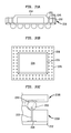
- FIG. 7 is a top elevation view illustrating a microelectronic package according to an embodiment of the invention.
- FIG. 8 is a fragmentary top elevation view further illustrating a microelectronic package according to an embodiment of the invention.
- FIG. 9 is a top elevation view illustrating a microelectronic package including a lead frame type substrate according to an embodiment of the invention.
- FIG. 10 is a corresponding sectional view of the microelectronic package shown in FIG. 9 ;
- FIG. 11 is a sectional view of a microelectronic assembly including a plurality of microelectronic packages electrically connected together and reinforced with an underfill according to a variation of the embodiment shown in FIG. 6 ;
- FIG. 12 is a photographic image representing an assembly having bonds between wire bonds of a first component and solder masses of a second component attached thereto;
- FIG. 13A is a fragmentary sectional view illustrating a wire bond via in a microelectronic package according to an embodiment of the invention.
- FIG. 13B is a fragmentary sectional view illustrating a wire bond via in a microelectronic package according to an embodiment of the invention.
- FIG. 13C is an enlarged fragmentary sectional view illustrating a wire bond via in a microelectronic package according to the embodiment shown in FIG. 13B ;
- FIG. 13D is a fragmentary sectional view illustrating a wire bond via in a microelectronic package according to an embodiment of the invention.
- FIG. 13E is an enlarged fragmentary sectional view illustrating a wire bond via in a microelectronic package according to the embodiment shown in FIG. 13D ;
- FIG. 13F is a fragmentary sectional view illustrating a wire bond via in a microelectronic package according to an embodiment of the invention.
- FIG. 14A illustrates stages in a method of forming a metal wire segment prior to bonding the wire segment to a conductive element according to an embodiment of the invention
- FIG. 14B is a fragmentary plan view of a shaped wire portion from a position below a capillary face
- FIG. 14C is a sectional view of the shaped wire portion between the capillary face and the coining surface
- FIG. 15 further illustrates a method as depicted in FIG. 14 and a forming unit suitable for use in such method
- FIGS. 16A-16D are plan views illustrating movement of a bond tool relative to a forming element during shaping of a wire portion in accordance with an embodiment of the invention
- FIG. 16E is a top elevation view illustrating wire bonds formed according to an embodiment of the invention.
- FIGS. 17A, 17B and 17C are views from above a wirebonding assembly, further illustrating a process of shaping a wire portion and bonding the shaped wire portion according to an embodiment of the invention
- FIGS. 18A, 18B and 18C are views from above a wirebonding assembly, further illustrating a process of shaping a wire portion and bonding the shaped wire portion according to an embodiment of the invention
- FIG. 19 illustrates stages in a method of forming a metal wire segment prior to bonding the wire segment to a conductive element according to an embodiment of the invention
- FIGS. 20A and 20B are sectional views illustrating one stage and another stage subsequent thereto in a method of forming an encapsulation layer of a microelectronic package according to an embodiment of the invention
- FIG. 20C is an enlarged sectional view further illustrating the stage corresponding to FIG. 19 ;
- FIG. 21A is a sectional view illustrating a stage of fabricating an encapsulation layer of a microelectronic package according to an embodiment of the invention.
- FIG. 21B is a sectional view illustrating a stage of fabricating an encapsulation layer of a microelectronic package subsequent to the stage shown in FIG. 21A ;
- FIGS. 22A-22E illustrate yet another method of forming an encapsulation layer by molding in which unencapsulated portions of wire bonds protrude through the encapsulation layer.
- FIGS. 23A and 23B are fragmentary sectional views illustrating wire bonds according to another embodiment
- FIGS. 24A and 24B are sectional views of a microelectronic package according to a further embodiment.
- FIGS. 25A and 25B are sectional views of a microelectronic package according to a further embodiment
- FIG. 26 shows a sectional view of a microelectronic package according to another embodiment
- FIGS. 27A-C are sectional views showing examples of embodiments of microelectronic packages according to further embodiments.
- FIGS. 28A-D show various embodiments of microelectronic packages during steps of forming a microelectronic assembly according to an embodiment of the disclosure
- FIG. 29 shows another embodiment of microelectronic packages during steps of forming a microelectronic assembly according to an embodiment of the disclosure
- FIGS. 30 A-C show embodiments of microelectronic packages during steps of forming a microelectronic assembly according to another embodiment of the disclosure
- FIGS. 31 A-C show embodiments of microelectronic packages during steps of forming a microelectronic assembly according to another embodiment of the disclosure
- FIGS. 32A and 32B show a portion of a machine that can be used in forming various wire bond vias in various stages of a method according to another embodiment of the present disclosure
- FIG. 33 shows a portion of a machine that can be used in forming various wire bond vias according in a method according to another embodiment of the present disclosure
- FIGS. 34A-C show various forms of an instrument that can be used in a method for making wire bonds according to an embodiment of the present disclosure
- FIG. 35 shows a portion of a machine that can be used in forming various wire bond vias according in a method according to another embodiment of the present disclosure
- FIG. 36 shows a portion of a machine that can be used in forming various wire bond vias according in a method according to another embodiment of the present disclosure
- FIGS. 37 A-D show sectional views illustrating stages of fabricating a microelectronic package according to an embodiment of the present disclosure
- FIGS. 38A and 38B show sectional views illustrating stages of fabricating a microelectronic package according to another embodiment of the present disclosure.
- FIGS. 39A-C show sectional views illustrating stages of fabricating a microelectronic package according to another embodiment of the present disclosure.
- FIG. 1 a microelectronic assembly 10 according to an embodiment of the present invention.
- the embodiment of FIG. 1 is a microelectronic assembly in the form of a packaged microelectronic element such as a semiconductor chip assembly that is used in computer or other electronic applications.
- the microelectronic assembly 10 of FIG. 1 includes a substrate 12 having a first surface 14 and a second surface 16 .
- the substrate 12 typically is in the form of a dielectric element, which is substantially flat.
- the dielectric element may be sheet-like and may be thin.
- the dielectric element can include one or more layers of organic dielectric material or composite dielectric materials, such as, without limitation: polyimide, polytetrafluoroethylene (“PTFE”), epoxy, epoxy-glass, FR-4, BT resin, thermoplastic, or thermoset plastic materials.
- the substrate may be a substrate of a package having terminals for further electrical interconnection with a circuit panel, e.g., a circuit board. Alternatively, the substrate can be a circuit panel or circuit board.
- the substrate can be a module board of a dual-inline memory module (“DIMM”).
- the substrate can be a microelectronic element such as may be or include a semiconductor chip embodying a plurality of active devices, e.g., in form of an integrated circuit or otherwise.
- the first surface 14 and second surface 16 are preferably substantially parallel to each other and are spaced apart at a distance perpendicular to the surfaces 14 , 16 defining the thickness of the substrate 12 .
- the thickness of substrate 12 is preferably within a range of generally acceptable thicknesses for the present application. In an embodiment, the distance between the first surface 14 and the second surface 16 is between about 25 and 500 ⁇ m.
- the first surface 14 may be described as being positioned opposite or remote from second surface 16 . Such a description, as well as any other description of the relative position of elements used herein that refers to a vertical or horizontal position of such elements is made for illustrative purposes only to correspond with the position of the elements within the Figures, and is not limiting.
- substrate 12 is considered as divided into a first region 18 and a second region 20 .
- the first region 18 lies within the second region and includes a central portion of the substrate 12 and extends outwardly therefrom.
- the second region 20 substantially surrounds the first region 18 and extends outwardly therefrom to the outer edges of the substrate 12 .
- no specific characteristic of the substrate itself physically divides the two regions; however, the regions are demarked for purposes of discussion herein with respect to treatments or features applied thereto or contained therein.
- a microelectronic element 22 can be mounted to first surface 14 of substrate 12 within first region 18 .
- Microelectronic element 22 can be a semiconductor chip or another comparable device.
- microelectronic element 22 is mounted to first surface 14 in what is known as a conventional or “face-up” fashion.
- wire leads 24 can be used to electrically connect microelectronic element 22 to some of a plurality of conductive elements 28 exposed at first surface 14 .
- Wire leads 24 can also be joined to traces (not shown) or other conductive features within substrate 12 that are, in turn, connected to conductive elements 28 .
- Conductive elements 28 include respective “contacts” or pads 30 that are exposed at the first surface 14 of substrate 12 .
- an electrically conductive element when an electrically conductive element is described as being “exposed at” the surface of another element having dielectric structure, it indicates that the electrically conductive structure is available for contact with a theoretical point moving in a direction perpendicular to the surface of the dielectric structure toward the surface of the dielectric structure from outside the dielectric structure.
- a terminal or other conductive structure that is exposed at a surface of a dielectric structure may project from such surface; may be flush with such surface; or may be recessed relative to such surface and exposed through a hole or depression in the dielectric.
- the conductive elements 28 can be flat, thin elements in which pad 30 is exposed at first surface 14 of substrate 12 .
- conductive elements 28 can be substantially circular and can be interconnected between each other or to microelectronic element 22 by traces (not shown).
- Conductive elements 28 can be formed at least within second region 20 of substrate 12 . Additionally, in certain embodiments, conductive elements 28 can also be formed within first region 18 . Such an arrangement is particularly useful when mounting microelectronic element 122 ( FIG.
- conductive elements 28 are formed from a solid metal material such as copper, gold, nickel, or other materials that are acceptable for such an application, including various alloys including one or more of copper, gold, nickel or combinations thereof.
- conductive elements 28 can be interconnected to corresponding second conductive elements 40 , such as conductive pads, exposed at second surface 16 of substrate 12 .
- Such an interconnection can be completed using vias 41 formed in substrate 12 that can be lined or filled with conductive metal that can be of the same material as conductive elements 28 and 40 .
- conductive elements 40 can be further interconnected by traces on substrate 12 .
- Microelectronic assembly 10 further includes a plurality of wire bonds 32 joined to at least some of the conductive elements 28 , such as on the pads 30 thereof.
- wire bonds 32 may be formed of wire, e.g., of copper or copper alloy, gold, aluminum, or a combination of a base wire metal, e.g., copper, copper alloy, gold or aluminum with a metallic coating finish or layer thereon of a different metal, which in some cases may be gold or palladium.
- the wire may have a diameter ranging from 10 micrometers and up, in more specific examples, can be 17 micrometers, 25 micrometers or greater, e.g., 35 micrometers or 50 micrometers. Where the microelectronic assembly 10 requires a large number of interconnects, or input or output connections, to the microelectronic assembly, there may be 1000-2000 wire bonds 32 as an example.
- Wire bonds 32 are bonded along a portion of the edge surface 37 thereof to the conductive elements 28 .
- Examples of such bonding include stitch bonding, wedge bonding and the like.
- a wire bonding tool can be used to stitch-bond a segment of wire extending from a capillary of the wire bonding tool to a conductive element 28 while severing the stitch-bonded end of the wire from a supply of wire in the capillary.
- the wire bonding tool may leave a mark (not shown) near the tip of the wire bonds 32 resulting from a process of forming the wire bond.
- the mark may result in a tapered region of the wire bond and/or have any geometric shape including a ball-shape.
- wire bonds are stitch-bonded to the conductive elements 28 at their respective “bases” 34 .
- the “base” 34 of such stitch-bonded wire bond 32 refers to the portion of the wire bond which forms a joint with the conductive element 28 .
- wire bonds can be joined to at least some of the conductive elements using ball bonds, examples of which are shown and described in co-pending, commonly assigned U.S. patent application, the entire disclosure of which is incorporated by reference herein.
- conductive elements 28 can be non-solder-mask-defined (“NSMD”) type conductive elements.
- NSMD non-solder-mask-defined
- the conductive elements are solder-mask defined. That is the conductive elements are exposed in openings formed in a solder mask material layer. In such an arrangement, the solder mask layer can partially overlie the conductive elements or can contact the conductive elements along an edge thereof.
- a NSMD conductive element is one that is not contacted by a solder mask layer.
- the conductive element can be exposed on a surface of a substrate that does not have a solder mask layer or, if present, a solder mask layer on the surface can have an opening with edges spaced away from the conductive element.
- NSMD conductive elements can also be formed in shapes that are not round. Solder-mask defined pads can often be round when intended to be used to bond to an element via a solder mass, which forms a generally round profile on such a surface. When using, for example, an edge bond to attach to a conductive element, the bond profile itself is not round, which can allow for a non-round conductive element.
- Such non-round conductive elements can be, for example oval, rectangular, or of a rectangular shape with rounded corners.
- the conductive elements 28 can be between about 10% and 25% larger than the intended size of base 34 in both directions. This can allow for variations in the precision with which the bases 34 are located and for variations in the bonding process.
- an edge bonded wire bond as described above, which can be in the form of a stitch bond, can be combined with a ball bond.
- a ball bond 1333 can be formed on a conductive element 1328 and a wire bond 1332 can be formed with a base 1338 stitch bonded along a portion of the edge surface 1337 to ball bond 1372 .
- the general size and placement of the ball bond can be as shown at 1372 ′.
- a wire bond 1332 can be edge bonded along conductive element 1328 , such as by stitch bonding, as described above.
- a ball bond 1373 can then be formed on top of the base 1338 of wire bond 1334 .
- the size and placement of the ball bond can be as shown at 1373 ′.
- Each of the wire bonds 32 can extend to a free end 36 remote from the base 34 of such wire bond and remote from substrate 12 .
- the ends 36 of wire bonds 32 are characterized as being free in that they are not electrically connected or otherwise joined to microelectronic element 22 or any other conductive features within microelectronic assembly 10 that are, in turn, connected to microelectronic element 22 .
- free ends 36 are available for electronic connection, either directly or indirectly as through a solder ball or other features discussed herein, to a conductive feature external to assembly 10 .
- ends 36 are held in a predetermined position by, for example, encapsulation layer 42 or otherwise joined or electrically connected to another conductive feature does not mean that they are not “free” as described herein, so long as any such feature is not electrically connected to microelectronic element 22 .
- base 34 is not free as it is either directly or indirectly electrically connected to microelectronic element 22 , as described herein.
- the bases 34 of the wire bonds 32 typically are curved at their stitch-bond (or other edge-bonded) joints with the respective conductive elements 28 .
- Each wire bond has an edge surface 37 extending between the base 34 thereof and the end 36 of such wire bond.
- base 34 can vary according to the type of material used to form wire bond 32 , the desired strength of the connection between wire bond 32 and conductive element 28 , or the particular process used to form wire bond 32 .
- Alternative embodiments are possible where wire bonds 32 are additionally or alternatively joined to conductive elements 40 exposed on second surface 16 of substrate 12 , extending away therefrom.
- a first one of the wire bonds 32 may be adapted, i.e., constructed, arranged, or electrically coupled to other circuitry on the substrate for carrying a first signal electric potential, and a second one of the wire bonds 32 may be so adapted for simultaneously carrying a second signal electric potential different from the first signal electric potential.
- the first and second wire bonds can simultaneously carry first and second different signal electric potentials.
- Wire bond 32 can be made from a conductive material such as copper, copper alloy or gold. Additionally, wire bonds 32 can be made from combinations of materials, such as from a core of a conductive material, such as copper or aluminum, for example, with a coating applied over the core. The coating can be of a second conductive material, such as aluminum, nickel or the like. Alternatively, the coating can be of an insulating material, such as an insulating jacket.
- the wire bonds may have a core of primary metal and a metallic finish including a second metal different from the primary metal overlying the primary metal.
- the wire bonds may have a primary metal core of copper, copper alloy, aluminum or gold and the metallic finish can include palladium. Palladium can avoid oxidation of a core metal such as copper, and may serve as a diffusion barrier to avoid diffusion a solder-soluble metal such as gold in solder joints between unencapsulated portions of the wire bonds and another component as will be described further below.
- the wire bonds can be formed of palladium-coated copper wire or palladium-coated gold wire which can be fed through the capillary of the wire bonding tool.
- the wire used to form wire bonds 32 can have a thickness, i.e., in a dimension transverse to the wire's length, of between about 15 ⁇ m and 150 ⁇ m.
- a wire bond is formed on a conductive element, such as conductive element 28 , a pad, trace or the like, using specialized equipment that is known in the art.
- the free end 36 of wire bond 32 has an end surface 38 .
- End surface 38 can form at least a part of a contact in an array formed by respective end surfaces 38 of a plurality of wire bonds 32 .
- FIG. 2 shows an exemplary pattern for such an array of contacts formed by end surfaces 38 .
- Such an array can be formed in an area array configuration, variations of which could be implemented using the structures described herein.
- Such an array can be used to electrically and mechanically connect the microelectronic assembly 10 to another microelectronic structure, such as to a printed circuit board (“PCB”), or to other packaged microelectronic elements, an example of which is shown in FIG. 6 .
- PCB printed circuit board
- wire bonds 32 and conductive elements 28 and 40 can carry multiple electronic signals therethrough, each having a different signal potential to allow for different signals to be processed by different microelectronic elements in a single stack.
- Solder masses 52 can be used to interconnect the microelectronic assemblies in such a stack, such as by electronically and mechanically attaching end surfaces 38 to conductive elements 40 .
- Microelectronic assembly 10 further includes an encapsulation layer 42 formed from a dielectric material.
- encapsulation layer 42 is formed over the portions of first surface 14 of substrate 12 that are not otherwise covered by or occupied by microelectronic element 22 , or conductive elements 28 .
- encapsulation layer 42 is formed over the portions of conductive elements 28 , including pad 30 thereof, that are not otherwise covered by wire bonds 32 .
- Encapsulation layer 42 can also substantially cover microelectronic element 22 , wire bonds 32 , including the bases 34 and at least a portion of edge surfaces 37 thereof.
- a portion of wire bonds 32 can remain uncovered by encapsulation layer 42 , which can also be referred to as unencapsulated portions 39 , thereby making the wire bond available for electrical connection to a feature or element located outside of encapsulation layer 42 .
- end surfaces 38 of wire bonds 32 remain uncovered by encapsulation layer 42 within major surface 44 of encapsulation layer 42 .
- Other embodiments are possible in which a portion of edge surface 37 is uncovered by encapsulation layer 42 in addition to or as an alternative to having end surface 38 remain uncovered by encapsulation layer 42 .
- encapsulation layer 42 can cover all of microelectronic assembly 10 from first surface 14 and above, with the exception of a portion of wire bonds 36 , such as end surfaces 38 , edge surfaces 37 or combinations of the two.
- a surface, such as major surface 44 of encapsulation layer 42 can be spaced apart from first surface 14 of substrate 12 at a distance great enough to cover microelectronic element 22 .
- embodiments of microelectronic assembly 10 in which ends 38 of wire bonds 32 are flush with surface 44 will include wire bonds 32 that are taller than the microelectronic element 22 , and any underlying solder bumps for flip chip connection.
- Other configurations for encapsulation layer 42 are possible.
- the encapsulation layer can have multiple surfaces with varying heights. In such a configuration, the surface 44 within which ends 38 are positioned can be higher or lower than an upwardly facing surface under which microelectronic element 22 is located.
- Encapsulation layer 42 serves to protect the other elements within microelectronic assembly 10 , particularly wire bonds 32 . This allows for a more robust structure that is less likely to be damaged by testing thereof or during transportation or assembly to other microelectronic structures.
- Encapsulation layer 42 can be formed from a dielectric material with insulating properties such as that described in U.S. Patent App. Pub. No. 2010/0232129, which is incorporated by reference herein.
- FIG. 3 shows an embodiment of microelectronic assembly 110 having wire bonds 132 with ends 136 that are not positioned directly above the respective bases 34 thereof. That is, considering first surface 114 of substrate 112 as extending in two lateral directions, so as to substantially define a plane, end 136 or at least one of the wire bonds 132 is displaced in at least one of these lateral directions from a corresponding lateral position of base 134 . As shown in FIG. 3 , wire bonds 132 can be substantially straight along the longitudinal axis thereof, as in the embodiment of FIG. 1 , with the longitudinal axis being angled at an angle 146 with respect to first surface 114 of substrate 112 . Although the cross-sectional view of FIG.
- wire bond 132 can also be angled with respect to first surface 114 in another plane perpendicular to both that first plane and to first surface 114 .
- Such an angle can be substantially equal to or different than angle 146 . That is the displacement of end 136 relative to base 134 can be in two lateral directions and can be by the same or a different distance in each of those directions.
- various ones of wire bonds 132 can be displaced in different directions and by different amounts throughout the assembly 110 .
- Such an arrangement allows for assembly 110 to have an array that is configured differently on the level of surface 144 compared to on the level of substrate 12 .
- an array can cover a smaller overall area or have a smaller pitch on surface 144 compared to that at first surface 114 of substrate 112 .
- some wire bonds 132 can have ends 138 that are positioned above microelectronic element 122 to accommodate a stacked arrangement of packaged microelectronic elements of different sizes.
- wire bonds 132 can be configured such that the end of one wire bond is positioned substantially above the base of a second wire bond, wherein the end of that second wire bond being positioned elsewhere.
- wire bonds 132 can be configured such that the end 136 A of one wire bond 132 A is positioned substantially above the base 134 B of another wire bond 134 B, the end 132 B of that wire bond 134 B being positioned elsewhere.
- Such an arrangement can be referred to as changing the relative position of a contact end surface 136 within an array of contacts, compared to the position of a corresponding contact array on second surface 116 .
- Curved portion 248 can take on a variety of shapes, as needed, to achieve the desired positions of the ends 236 of the wire bonds 232 .
- curved portions 248 can be formed as S-curves of various shapes, such as that which is shown in FIG. 4 or of a smoother form (such as that which is shown in FIG. 5 ). Additionally, curved portion 248 can be positioned closer to base 234 than to end 236 or vice-versa. Curved portion 248 can also be in the form of a spiral or loop, or can be compound including curves in multiple directions or of different shapes or characters.
- the wire bonds 132 can be arranged such that the bases 134 are arranged in a first pattern having a pitch thereof.
- the wire bonds 132 can be configured such that the unencapsulated portions thereof 139 including end surfaces 138 , can be disposed at positions in a pattern having a minimum pitch between adjacent unencapsulated portions 38 of the wire bonds 32 exposed at the surface 44 of the encapsulation layer that is greater than the minimum pitch between adjacent bases of the plurality of bases 134 and, accordingly, the conductive elements 128 to which the bases are joined).
- the wire bonds can include portions which extend in one or more angles relative to a normal direction to the conductive elements, such as shown in FIG. 26 .
- the wire bonds can be curved as shown, for example in FIG. 4 , such that the ends 238 are displaced in one or more lateral directions from the bases 134 , as discussed above.
- the conductive elements 128 and the ends 138 can be arranged in respective rows or columns and the lateral displacement of end surfaces 138 at some locations, such as in one row of the ends, from the respective conductive elements on the substrate to which they are joined can be greater than the lateral displacement of the unencapsulated portions at other locations from the respective conductive elements to which they are connected.
- the wire bonds 132 can, for example be at different angles 146 A, 146 B with respect to the surface 116 of the substrate 112 .
- the wire bonds 332 Ci and 332 Cii also shows an exemplary pair of such wire bonds 332 Ci and 332 Cii that have bases 334 Ci and 334 Cii positioned in the same row of a substrate-level array and ends 336 Ci and 336 Cii that are positioned in different rows of a corresponding surface-level array.
- the radius of bends in the wire bonds 332 Ci, 332 Cii can be large such that the curves in the wire bonds may appear continuous.
- the radius of the bends may be relatively small, and the wire bonds may even have straight portions or relatively straight portions between bends in the wire bonds.
- the unencapsulated portions of the wire bonds can be displaced from their bases by at least one minimum pitch between the contacts 328 of the substrate. In other cases, the unencapsulated portions of the wire bonds can be displaced from their bases by at least 200 micrometers.
- a further variation of a wire bond 332 D is shown that is configured to be uncovered by encapsulation layer 342 on a side surface 47 thereof.
- free end 336 D is uncovered, however, a portion of edge surface 337 D can additionally or alternatively be uncovered by encapsulation layer 342 .
- Such a configuration can be used for grounding of microelectronic assembly 10 by electrical connection to an appropriate feature or for mechanical or electrical connection to other featured disposed laterally to microelectronic assembly 310 .
- FIG. 5 shows an area of encapsulation layer 342 that has been etched away, molded, or otherwise formed to define a recessed surface 345 that is positioned closer to substrate 12 than major surface 342 .
- FIG. 5A further shows a microelectronic assembly 310 having two microelectronic elements 322 and 350 in an exemplary arrangement where microelectronic element 350 is stacked, face-up, on microelectronic element 322 .
- leads 324 are used to electrically connect microelectronic element 322 to conductive features on substrate 312 .
- Various leads are used to electronically connect microelectronic element 350 to various other features of microelectronic assembly 310 .
- lead 380 electrically connects microelectronic element 350 to conductive features of substrate 312
- lead 382 electrically connects microelectronic element 350 to microelectronic element 322 .
- An opening can be formed in encapsulation layer 342 that extends from surface 344 thereof to a point along, for example, lead 380 , thereby providing access to lead 380 for electrical connection thereto by an element located outside surface 344 .
- a similar opening can be formed over any of the other leads or wire bonds 332 , such as over wire bonds 332 C at a point away from the ends 336 C thereof.
- ends 336 C can be positioned beneath surface 344 , with the opening providing the only access for electrical connection thereto.
- FIG. 27B shows an arrangement where a first microelectronic element 1722 is face-up mounted on surface 1714 and connected through wire bonds 1788 to conductive elements 1728 .
- Second microelectronic element 1750 can have contacts exposed at a face thereof which face and are joined to corresponding contacts at a face of the first microelectronic element 1722 which faces away from the substrate. Through a set of contacts 1726 of the second microelectronic element 1750 which face and are joined to corresponding contacts on the front face of the first microelectronic element 1722 .
- These contacts of the first microelectronic element 1722 which are joined to corresponding contacts of the second microelectronic element can in turn be connected through circuit patterns of the first microelectronic element 1722 and be connected by ire bonds 1788 to the conductive elements 1728 on substrate 1712 .
- FIG. 27C shows an example in which first and second microelectronic elements 1822 , 1850 are spaced apart from one another in a direction along a surface 1814 of substrate 1812 .
- Either one or both of the microelectronic elements (and additional microelectronic elements) can be mounted in face-up or flip-chip configurations described herein.
- any of the microelectronic elements employed in such an arrangement can be connected to each other through circuit patterns on one or both such microelectronic elements or on the substrate or on both, which electrically connect respective conductive elements 1828 to which the microelectronic elements are electrically connected.
- FIG. 5B further illustrates a structure according to a variation of the above-described embodiments in which a second conductive element 43 can be formed in contact with an unencapsulated portion 39 of a wire bond exposed at or projecting above a surface 44 of the encapsulation layer 42 , the second conductive element not contacting the first conductive element 28 ( FIG. 1 ).
- the second conductive element can include a pad 45 extending onto a surface 44 of the encapsulation layer which can provide a surface for joining with a bonding metal or bonding material of a component thereto.
- the second conductive element 43 or 48 can include or be formed of a conductive paste contacting the unencapsulated portion 39 of the wire bond.
- stenciling, dispensing, screen printing, controlled spraying, e.g., a process similar to inkjet printing, or transfer molding can be used to form second conductive elements 43 or 48 on the unencapsulated portions 39 of the wire bonds.
- FIG. 5D further illustrates a second conductive element 43 D which can be formed of a metal or other electrically conductive material as described for conductive elements 43 , 48 above, wherein the second conductive element 43 D is formed at least partly within an opening 49 extending into an exterior surface 44 of the encapsulation layer 42 .
- the opening 49 can be formed by removing a portion of the encapsulation layer after curing or partially curing the encapsulation layer so as to simultaneously expose a portion of the wire bond thereunder which then becomes the unencapsulated portion of the wire bond.
- the opening 49 can be formed by laser ablation, etching.
- a soluble material can be pre-placed at the location of the opening prior to forming the encapsulation layer and the pre-placed material then can be removed after forming the encapsulation layer to form the opening.
- multiple wire bonds 1432 can have bases joined with a single conductive element 1428 .
- Such a group of wire bonds 1432 can be used to make additional connection points over the encapsulation layer 1442 for electrical connection with conductive element 1428 .
- the exposed portions 1439 of the commonly-joined wire bonds 1432 can be grouped together on surface 1444 of encapsulation layer 1442 in an area, for example about the size of conductive element 1428 itself or another area approximating the intended size of a bonding mass for making an external connection with the wire bond 1432 group.
- such wire bonds 1432 can be either ball-bonded ( FIG. 24A ) or edge bonded ( FIG. 24B ) on conductive element 1428 , as described above, or can be bonded to the conductive element as described above with respect to FIG. 23A or 23B or both.
- ball-bonded wire bonds 1532 can be formed as stud bumps on at least some of the conductive elements 1528 .
- a stud bump is a ball-bonded wire bond where the segment of wire extending between the base 1534 and the end surface 1538 has a length of at most 300% of the diameter of the ball-bonded base 1534 .
- the end surface 1538 and optionally a portion of the edge surface 1537 of the stud bump can be unencapsulated by the encapsulation layer 1542 . As shown in FIG.
- such a stud bump 1532 A can be formed on top of another stud bump 1532 B to form, essentially, a base 1534 of a wire bond 1532 made up of the two ball bonds with a wire segment extending therefrom up to the surface 1544 of the encapsulation layer 1542 .
- wire bonds 1532 can have a height that is less than, for example, the wire bonds described elsewhere in the present disclosure.
- the encapsulation layer can include a major surface 1544 in an area, for example overlying the microelectronic element 1522 and a minor surface 1545 spaced above the surface 1514 of the substrate 1512 at a height less than that of the major surface 1544 .
- Such arrangements can also be used to form alignment features and to reduce the overall height of a package employing stud bump type wire bonds as well as other types of wire bonds disclosed herein, while accommodating conductive masses 1552 that can connect the unencapsulated portions 1539 of the wire bonds 1532 with contacts 1543 on another microelectronic package 1588 .
- wire bonds 432 are configured with a curved portion 448 such that at least some of the ends 436 of the wire bonds 432 extend into an area that overlies a major surface 424 of the microelectronic element 422 .
- Such an area can be defined by the outer periphery of microelectronic element 422 and extending upwardly therefrom.
- An example of such a configuration is shown from a view facing toward first surface 414 of substrate 412 in FIG. 18 , where wire bonds 432 overlie a rear major surface of the microelectronic element 422 , which is flip-chip bonded at a front face 425 thereof to substrate 412 .
- FIG. 18 In another configuration ( FIG.
- the microelectronic element 422 can be mounted face-up to the substrate 312 , with the front face 325 facing away from the substrate 312 and at least one wire bond 336 overlying the front face of microelectronic element 322 .
- wire bond 336 is not electrically connected with microelectronic element 322 .
- a wire bond 336 bonded to substrate 312 may also overlie the front or rear face of microelectronic element 350 .
- conductive elements 428 are arranged in a pattern forming a first array in which the conductive elements 428 are arranged in rows and columns surrounding microelectronic element 422 and may have a predetermined pitch between individual conductive elements 428 .
- Wire bonds 432 are joined to the conductive elements 428 such that the respective bases 434 thereof follow the pattern of the first array as set out by the conductive elements 428 .
- Wire bonds 432 are configured, however, such that the respective ends 436 thereof can be arranged in a different pattern according to a second array configuration. In the embodiment shown the pitch of the second array can be different from, and in some cases finer than that of the first array.
- FIG. 6 further shows an insulating layer 421 extending along a surface of microelectronic element 422 .
- Insulating layer 421 can be formed from a dielectric or other electrically insulating material prior to forming the wire bonds.
- the insulating layer 421 can protect microelectronic element from coming into contact with any of wire bonds 423 that extend thereover.
- insulating layer 421 can avoid electrical short-circuiting between wire bonds and short-circuiting between a wire bond and the microelectronic element 422 . In this way, the insulating layer 421 can help avoid malfunction or possible damage due to unintended electrical contact between a wire bond 432 and the microelectronic element 422 .
- microelectronic assembly 410 can connect to another microelectronic assembly, such as microelectronic assembly 488 , in certain instances where the relative sizes of, for example, microelectronic assembly 488 and microelectronic element 422 would not otherwise permit.
- microelectronic assembly 488 is sized such that some of the contact pads 440 are in an array within an area smaller than the area of the front or rear surface 424 or 426 of the microelectronic element 422 .
- substantially vertical conductive features, such as pillars in place of wire bonds 432 , direct connection between conductive elements 428 and pads 440 would not be possible.
- FIGS. 9 and 10 show a further embodiment of a microelectronic assembly 510 in which wire bonds 532 are formed on a lead-frame structure.
- lead frame structures are shown and described in U.S. Pat. Nos. 7,176,506 and 6,765,287 the disclosures of which are hereby incorporated by reference herein.
- a lead frame is a structure formed from a sheet of conductive metal, such as copper, that is patterned into segments including a plurality of leads and can further include a paddle, and a frame. The frame is used to secure the leads and the paddle, if used, during fabrication of the assembly.
- a microelectronic element such as a die or chip
- the microelectronic element can be joined face-up to the paddle and electrically connected to the leads using wire bonds.
- the microelectronic element can be mounted directly onto the leads, which can extend under the microelectronic element.
- contacts on the microelectronic element can be electrically connected to respective leads by solder balls or the like.
- the leads can then be used to form electrical connections to various other conductive structures for carrying an electronic signal potential to and from the microelectronic element.
- temporary elements of the frame can be removed from the leads and paddle of the lead frame, so as to form individual leads.
- Encapsulation layer 542 is formed onto assembly 510 leaving ends 538 of wire bonds 532 uncovered at locations within surface 544 .
- Wire bonds 532 can have additional or alternative portions thereof uncovered by encapsulation layer 542 in structures that correspond to those described with respect to the other embodiments herein.
- portions of the underfill 620 that extend along the edge surfaces of the packages 610 A, 610 B, if any, can be disposed at an angle between 0° and 90° relative to a major surface of the circuit panel over which the packages are disposed, and can be tapered from a greater thickness adjacent the circuit panel to a smaller thickness at a height above the circuit panel and adjacent one or more of the packages.
- a package arrangement shown in FIGS. 28A-D can be implemented in one technique for making an underfill layer, and in particular a portion thereof that is disposed between confronting faces of packages 1910 A and 1910 B, such as surface 1942 of package 1910 A and surface 1916 of package 1910 B.
- package 1910 A can extend beyond an edge surface 1947 of package 1910 B such that, for example, the surface 1944 of encapsulation layer 1942 has a portion thereof that is exposed outside of package 1910 B.
- Such an area can be used as a dispensing area 1949 whereby a device can deposit an underfill material in a flowable state on the dispensing area from a vertical position relative thereto.
- the dispensing area 1949 can be sized such that the underfill material can be deposited in a mass on the surface without spilling off of the edge of the surface while reaching a sufficient volume to flow under package 1910 B where it can be drawn by capillary into the area between the confronting surfaces of packages 1910 A and 1910 B, including around any joints therebetween, such as solder masses or the like.
- additional material can be deposited on the dispensing area such that a continuous flow is achieved that does not significantly spill over the edge of package 1910 A. As shown in FIG.
- the dispensing area 1949 can surround package 1910 B and have a dimension D in an orthogonal direction away from a peripheral edge of package 1910 B of about one millimeter (1 mm) on each side thereof. Such an arrangement can allow for dispensing on one side of package 1910 B or more than one side, either sequentially or simultaneously.
- Alternative arrangements are shown in FIG. 28C , wherein the dispensing area 1949 extends along only two adjacent sides of package 1910 B and have a dimension D′ of about 1 mm in a direction orthogonally away from a peripheral edge of the second package, and FIG. 28D , wherein the dispensing area 1949 extends along a single side of package 1910 B and may have a dimension D′′ in an orthogonal direction away from the peripheral edge of the package of, for example 1.5 mm to 2 mm.
- the bezel 2099 can be of a resiliently compliant material such as rubber, TPE, PTFE (polytetrafluoroethylene), silicone or the like and can be undersized relative to the size of the assembled packages such that a compressive force is applied by the bezel when in place.
- the bezel 2099 can also be left in place during the application of an underfill material and can include an opening to accommodate such application therethrough.
- the compliant bezel 2099 can be removed after package assembly.
- a lower package 2110 A can include at least one alignment surface 2151 .
- alignment surfaces 2151 are included in encapsulation layer 2142 near the corners of the package 2110 B.
- the alignment surfaces are sloped relative to the major surface and define an angle of between about 0° and up to and including 90° relative to major surface 2144 at some location therefrom, the alignment surfaces extending locations proximate the major surface 2144 and respective minor surfaces 2145 that are spaced above substrate 2112 at a greater distance than major surface 2144 .
- the minor surfaces 2145 can be disposed adjacent the corners of package 2110 A and can extend partially between intersecting sides thereof. As shown in FIG. 30B , the alignment surfaces can also form inside corners opposite the intersecting sides of the package 2110 A and can be included in similar form along all corners, for example four corners, of package 2110 A. As illustrated in FIG.
- FIGS. 31A-C A further arrangement employing alignment surfaces 2251 is shown in FIGS. 31A-C , wherein the alignment surfaces 2251 extend between a raised inner surface 2244 to a lower outer surface 2245 .
- inner surface 2244 can overlie microelectronic element 2222 and can be spaced above substrate 2212 accordingly.
- Outer surface 2245 can be spaced closer to substrate 2212 in a direction of the thickness of the substrate and can be positioned vertically between surface 2214 of substrate 2212 and surface 2223 of microelectronic element 2222 .
- One or more unencapsulated portions of wire bonds 2232 can be positioned relative to the alignment surfaces 2251 to achieve alignment of solder balls 2252 or other conductive protrusion as described with respect to FIGS. 30A-C .
- such a stepped arrangement can be used with or without the described alignment functionality to achieve an overall lower assembly height given a certain bond mass size.
- the incorporation of a raised inner surface 2244 can lead to increased resistance of package 2210 A to warping.
- FIGS. 13A, 13B, 13C, 13D, 13E and 13F illustrate some possible variations in the structure of the wire bonds 32 as described above relative to FIG. 1 .
- a wire bond 732 A may have an upwardly extending portion 736 which terminates in an end 738 A having the same radius as the radius of portion 736 .
- FIG. 13B illustrates a variation in which the ends 738 B are tips which are tapered relative to portion 736 .
- a tapered tip 738 B of a wire bond 732 A may have a centroid 740 which is offset in a radial direction 741 from an axis of a cylindrical portion of the wire bond integral therewith.
- Such shape may be a bonding tool mark resulting from a process of forming the wire bond as will be described further below.
- a bonding tool mark other than as shown at 738 B may be present on the unencapsulated portion of the wire bond.
- the unencapsulated portion 739 of a wire bond may project away from the substrate 712 at an angle 750 within 25 degrees of perpendicular to the surface 730 of the substrate on which the conductive elements 728 are disposed.
- FIG. 13D illustrates that an unencapsulated portion of a wire bond 732 D can include a ball-shaped portion 738 D.
- the ball-shaped portion 738 D can be integral with a cylindrical portion 736 of the wire bond 732 D, wherein the ball-shaped portion and at least a core of the cylindrical portion of the wire bond consist essentially of copper, copper alloy or gold.
- the ball-shaped portion can be formed by melting a portion of the wire exposed at an opening of the capillary of the bonding tool during a pre-shaping process before stitch-bonding the wire bond to a conductive element 728 of the substrate. As seen in FIG.
- the diameter 744 of the ball-shaped portion 738 D may be greater than the diameter 746 of the cylindrical wire bond portion 736 that is integral therewith.
- the cylindrical portion of a wire bond 732 D that is integral with the ball-shaped portion 738 D can project beyond a surface 752 of the encapsulant layer 751 of the package.
- the cylindrical portion of a wire bond 732 D may be fully covered by the encapsulant layer.
- the ball-shaped portion 738 D of the wire bond 732 D may in some cases be partly covered by the encapsulation layer 751 .
- FIG. 14A illustrates a method by which a wire bond ( FIG. 1 ) as described herein can be shaped as a wire portion extending from a face of a bonding tool 804 , e.g., from a face 806 of a capillary-type bonding tool 804 , prior to bonding the shaped wire portion 800 to a bonding surface, e.g., to a conductive element 28 on a substrate, as will be further described herein.
- a portion 800 of a wire i.e., an integral portion having a predetermined length 802 , of a metal wire such as a gold or copper wire or composite wire as described above described above relative to FIG.
- the bonding tool 804 can be a capillary having an opening in the face 806 thereof beyond which the wire portion extends.
- the bonding tool can be either be a capillary or a different type of bonding tool, such as an ultrasonic or thermosonic bonding tool or wedge-bonding tool, for example.
- the initial wire length can be set by using the bonding tool 804 to bond the wire to a bonding surface in a prior stage of processing, e.g., by a stitch-bonding method or by a ribbon-bonding method.
- the ribbon when employing the ribbo-bonding method, can be one or more flat surfaces, and can be polygonal in cross-section, such as a rectangular cross-section.
- the wire can be clamped at a location above the capillary face and the clamped wire then can be tensioned so as to cause the clamped wire to break adjacent to the bonded part of the wire and thereby free the end 838 of the wire portion 800 from the bonded second wire portion.
- the wire can be tensioned by exerting a force on at least one of the capillary or the bonding surface relative to the other, e.g., such as by pulling the capillary in an at least partially vertical direction relative to a direction the wire extends through the capillary.
- the wire portion 800 may extend in a straight direction 801 away from a face 806 of the capillary.
- the direction 801 may be perpendicular to the face 806 of the capillary.
- the capillary and a forming surface are positioned relative to one another such that an end 838 of the wire portion 800 that extends beyond the capillary face 806 is positioned at a greater depth 802 from the capillary face 806 than a depth 803 of the forming surface 812 below the capillary face.
- the forming element 810 may be one or more tools or elements which together have surfaces suitable to assist in the forming, i.e., shaping, of the wire portion prior to the wire portion being bonded to the conductive element of the substrate.
- the first forming surface 812 can be a surface within a groove extending in the first direction 814 along a forming element 810 , wherein the first direction can be parallel to the capillary face 806 .
- groove 815 can be open to a second surface 813 of the forming element which confronts the capillary face 806 .
- the wire portion 800 may extend into groove and may extend in the first direction parallel to the surface 812 and parallel to a direction 814 of movement of the capillary 804 as seen at stage B of FIG. 14A .
- the capillary 804 can be moved in a second direction 817 which is transverse to directions parallel to the capillary face 806 .
- an exposed wall 820 of the capillary which extends away from the capillary face 806 may confront a second forming surface 864 .
- movement of the capillary 804 in direction 817 can cause the wire portion 800 to be bent in a direction towards the exposed wall 820 .
- the second forming surface 864 can be a surface of forming element 810 , the second forming surface 864 extending away from the first forming surface 812 .
- the second forming surface can extend at an angle 865 relative to the first forming surface 812 which may be the same as an angle 867 at which the exposed wall of the capillary extends relative to the capillary face 806 .
- the movement of the capillary can cause a part of the wire portion 800 to project upwardly in a direction 818 along the exposed wall 820 of the capillary.
- Capillary or bond tool 804 may have a groove, flat side or other wire-guiding feature on exposed wall thereof to help guide wire there.
- the second forming surface 864 can be vertical, i.e., at an angle normal to the face of the bonding tool, when the bonding tool has a vertical wall (as shown in FIG. 35 ).
- the wire portions 800 may be formed from copper or copper alloy, and may have relatively small diameter, e.g., 25 micrometers, such that a large number of input/output connections, e.g., 1000-2000 per package.
- Stage C illustrates further processing of the wire portion 800 by relative movement of the capillary 804 and a another forming surface 823 in a direction transverse to the capillary face 806 , for example, in direction 817 , or in a direction perpendicular to the face 806 of the capillary, the forming surface 823 , or perpendicular to both surfaces.
- the forming surface 823 can be considered a “coining surface.”
- FIG. 14B is a fragmentary plan view of a shaped wire portion 800 from a position below the capillary face 806 and FIG. 14C is a sectional view further illustrating the position of the wire portion 800 between the capillary face 806 and the coining surface 823 and parts of the wire portion as will be further described below.
- FIG. 14B illustrates the shaped wire portion from a position below the coining surface 823 and looking towards the coined part 825 of the wire portion 800 such that the capillary face 806 appears at a position above, i.e., behind the coined part 825 of the wire portion in FIG. 14B .
- a part 827 of the wire portion 800 aligned with the opening 808 in the capillary face is also illustrated in FIGS.
- FIGS. 14A-B A part 831 of the wire portion 800 which extends away from the capillary face 806 along the exposed wall 820 ( FIG. 14A ) of the capillary is also shown in FIGS. 14A-B .
- the parts 827 and 831 of the wire portion typically retain cylindrical cross-section after the processing described above in accordance with FIG. 14A , these parts 827 , 831 of the wire possibly avoiding some of the flattening of the wire when the part 825 of the wire portion 800 is coined between the capillary face 806 and the coining surface 823 .
- At least a part of a face 833 of the coined part 825 of the wire portion facing the coining surface 823 can also be flat. This flat face 833 then will be further available to be bonded by the capillary to a bonding surface of a conductive element 28 such as described above.
- the coining surface 823 may in some cases be patterned such that it has raised and recessed features therein.
- the face 833 of the coined part 825 of the wire portion may likewise be patterned face of raised and recessed features which faces away from the capillary face 806 .
- Such patterned face of the coined part 825 would then be available to be bonded to a bonding surface of a conductive element 28 .
- the capillary can be used to bond the pre-shaped wire portion 800 to a bonding surface of a conductive element 28 of a substrate ( FIG. 1 ).
- the wire is now moved away from the forming unit 810 and moved towards the conductive element 28 ( FIG. 1 ) of the substrate where the capillary then stitch bonds the coined wire portion 825 to the conductive element 28 , with the end 838 of the wire portion being the remote end 38 ( FIG. 1 ) of the wire bond remote from the conductive element 28 .
- a wire portion 800 having a coined part 825 with a lower surface 833 which can be flat, or alternatively, patterned, or a face that is partly flat and partly patterned, can assist in forming a good bond between the shaped wire portion 800 and the bonding surface of the conductive element 28 .
- the shaped wire portion 800 when ready for bonding to the bonding surface, is rather long relative to the diameter of the wire, and a long extension of the wire, being much if not most of the shaped wire portion is unsupported except by the bonding surface of the conductive element 28 ( FIG. 1 ) when the wire portion is being bonded thereto.
- the stability of the wire portion can be improved when the wire portion is being bonded to the bonding surface.
- the flattening or patterning of the coined part 825 of the wire may help increase friction between the lower surface 833 of the coined part 825 and the bonding surface when the capillary applies force to the wire portion to bond it to the bonding surface, and may decrease a tendency of the wire to pivot, roll or otherwise move when the bonding force is applied.
- the coined part 825 of the wire portion can overcome a possibility that the wire having the original cylindrical shape would pivot or roll when force is applied by the face 806 of a capillary to bond the wire to the bonding surface.
- the forming element 810 may have a first opening or depression 830 in which the capillary 804 is disposed at an initial stage ( FIG. 14A , stage A) of wire-shaping, when the wire portion 800 extends outwardly beyond an opening 808 of the capillary.
- the opening 830 or depression may include a tapered portion, channel or groove 832 which can help guide the wire portion 800 onto a surface 812 at stage B, and which may also guide the wire portion a particular portion of the surface 812 .
- Such tapered portion can be tapered in such way that the tapered portion grows smaller in a direction towards the surface 812 to help engage and guide the wire portion to a particular location.
- the forming unit may further include a channel 834 or groove for guiding the segment 800 in stage B of the process.
- the forming unit may include a further opening or depression or 840 in which an interior surface 816 thereof may function as the second forming surface along which the capillary moves in stage C of the process to cause the metal wire segment to be bent in direction 818 against the exterior wall 820 of the capillary.
- the second forming surface within the opening 816 or depression can include a channel or groove 819 which is recessed relative to another interior surface within the opening 816 .
- the coining surface 823 can be disposed within the opening 816 .
- a groove may be formed on the tool or on the capillary itself, in addition to or as an alternative to groove 819 .
- a groove 811 may be formed on the capillary face 806 in addition to or as an alternative to groove 819 .
- a variation of the capillary shown in FIG. 14 can be used that incorporates a vertical or near-vertical side wall 2820 .
- the side wall 2820 of capillary 2804 can be substantially vertical or, in other words, parallel to the wire segment 2800 or perpendicular to the face 2806 of the capillary 2804 .
- This can allow for formation of a wire bond ( 32 in FIG. 1 ) that is closer to vertical, i.e., closer to an angle of 90° away from the surface of the first surface of the substrate, than achieved by a side wall at an exterior of the capillary that defines an angle having a measure substantially less than 90°, such as the capillary shown in FIG. 14 .
- a wire bond can be achieved that is disposed at an angle from the first portion which extends between 25° and 90°, or between about 45° and 90° or between about 80° and 90° with respect to the first wire portion 2822 .
- a capillary 3804 can include a surface 3808 that projects beyond the face 3806 thereof. This surface 3808 can be included, for example over the edge of the side wall 3820 , and may form a lip.
- the capillary 3804 can be pressed against the first portion 3822 of the wire segment 3800 during forming of wire segment, e.g., when the capillary moves in a direction along a forming surface 3816 which extends in a direction away from surface 3812 .
- surface 3808 presses into the first portion 3822 at a location near the bend from which the remaining wire segment 3800 extends.
- the deformation from the surface 3808 can be such that a position of the wire segment 3800 can be substantially retained when the capillary 3804 is removed.
- FIGS. 16A-16C illustrate stages of shaping a wire and a set of forming surfaces used therein in a method of forming wire bonds according to an embodiment of the invention.
- FIG. 16A shows a forming element 850 which can be used in shaping a portion of a wire extending beyond a face of a bonding tool prior to forming a bond between the wire portion and a bonding surface of a substrate.
- the bonding tool can be a capillary type tool or other bonding tool such as an ultrasonic bonding tool or wedge-bonding tool.
- a recess 852 may extend in an inward direction from an edge 851 of the forming element 850 .
- the recess 852 can be configured to receive a portion of a wire extending from a face of a bonding tool, such as a wire portion extending from a face of the capillary or other type bonding tool.
- the recess may additionally include a tapered portion or channel 854 having width 855 somewhat larger than the diameter of a wire to be shaped therein. As a tapered portion, the width can become smaller in a direction towards the first forming surface 860 such that the tapered portion can help guide the wire towards a particular area 862 , e.g., a central area, of the first forming surface.
- the first forming surface may be a flat, i.e., planar or substantially planar surface which extends in first and second transverse directions, and area 862 of the first forming surface can likewise be flat. In such way, the first forming surface can extend in directions parallel to a face of the bonding tool or capillary when shaping the wire portion in stage of the method such as seen in stage B as seen in FIG. 14 .
- the forming element 850 typically also includes a second forming surface 864 which extends away from the first forming surface 860 .
- the second forming surface 864 extends away from the first forming surface 860 .
- the second forming surface 864 may be disposed in a second recess 866 extending inwardly from an edge 861 of the forming element opposite edge 851 .
- an angle 865 at which the second forming surface 864 slopes away from the first forming surface 860 can be the same as an angle 867 at which an exposed wall 868 of the bonding tool slopes away from the face of the bonding tool, as seen in FIG. 14A .
- the forming element 860 typically has an additional surface, which can be a “coining” surface 870 against which a face of the bonding tool or capillary can be pressed during the wire-shaping process to coin a part of the wire that is disposed between the face 806 of the bonding tool and the coining surface 870 .
- FIG. 16B illustrates a stage of shaping the wire portion 800 ( FIG. 14A ) when the capillary or other type bonding tool 804 has moved into a position in which the shaping of the wire portion extending beyond the bonding tool face is about to begin. At such time, the wire portion 800 extends into the recess 852 of the forming element 850 .
- FIG. 16B illustrates a stage of shaping the wire analogous to stage A shown in FIG. 14A , which further shows the direction 814 of movement of the bonding tool along the forming element 850 .
- FIG. 16C illustrates a further stage of shaping the wire portion 800 ( FIG. 14A ) when the bonding tool 804 has moved in direction 814 along a first forming surface 860 or 862 , these surfaces having been described above relative to FIG. 16A .
- a part 831 of the wire portion is shown extending away from an opening 808 of the bonding tool similar to the wire portion seen at stage B in FIG. 14A .
- FIG. 16D further illustrates a stage of shaping the wire analogous to that seen at stage C of FIG. 14A in which the bonding tool 804 has moved to a position aligned with a second recess in the forming element.
- the part 831 of the wire portion which extends away from the opening can be bent towards the exposed wall of the bonding tool, as shown and described above with respect to FIG. 14A .
- the bonding tool 804 can coin the wire portion by pressing a part of the wire portion between the face of the bonding tool and the coining surface, the coining surface 870 being as shown in FIG. 16A .
- 16E is a diagrammatic view showing that wire bonds 932 formed according to one or more of the methods described herein can have ends 938 which are offset from their respective bases 934 .
- an end 938 of a wire bond can be displaced from its respective base such that the end 938 is displaced in a direction parallel to the surface of the substrate beyond a periphery of the conductive element to which it is connected.
- an end 938 of a wire bond can be displaced from its respective base 934 such that the end 938 is displaced in a direction parallel to the surface of the substrate beyond a periphery 933 of the conductive element to which it is connected.
- FIGS. 17A-C illustrate an example of using a bonding tool to shape the wire portion at a forming station 880 .
- the forming station can be assembled with, e.g., mounted to a structure to which a wirebonding station is also assembled, so that a wire portion, after being shaped at the forming station by the bonding tool, can then be moved by the bonding tool to the wirebonding station and then bonded to a bonding surface on a substrate, microelectronic element or other component.
- a bond tool 804 portion of a bond head 844 can first be moved to the forming station 880 where the wire portion can be shaped by movement of the bond tool as described above.
- the bond head 844 or a portion of the bond head can pivot about an axis to move the bonding tool to the forming station 880 .
- the forming element 850 can be oriented in a specific way relative to the wirebonding station to reduce the extent of movement required by the bond head or bond tool between the forming station and wirebonding station. As seen in FIG. 17A , in one example, the forming element 850 at the forming station can be oriented such that the recess 852 described above relative to FIG. 16A may be at a remote position relative to the wirebonding station and the coining surface 870 may be at a position closer to, i.e., adjacent to the wirebonding station. In another example, the recess 852 and the coining surface 870 can be oriented in the opposite way with the recess 852 closer to the wirebonding station than the coining surface.
- the forming element may be in one orientation during the shaping of the wire portion, and then the orientation of the forming element can be reversed to permit greater freedom of movement of the bond tool with the shaped wire portion thereon prior to moving the shaped wire portion into final position for bonding.
- FIG. 17B illustrates a position of the bond tool 804 and bond head 844 at the completion of shaping the wire portion, which may include coining the wire portion as described above.
- the bond tool can then be moved from the position at the forming station 880 ( FIG. 17B ) into position ( FIG. 17C ) at the wirebonding station 882 where the shaped wire portion then is bonded to a bonding surface on a component 884 .
- FIGS. 18A-18C illustrate another variation in which the bond tool 1804 and a forming element 1810 , such as the forming element 810 or 850 as described above, can be assembled with a common bond head 1844 .
- the forming element 1810 can be affixed to or otherwise carried on the bond head 1844 such that movement of the bond head transports the forming element 1810 attached thereto as well as the bonding tool.
- the forming element 1810 can move relative to the bonding tool so as to assist in the shaping of the wire portion prior to bonding of the wire portion, but then the forming element 1810 can be moved away from such forming position once the wire has been shaped and is ready to be bonded to a component 1884 as seen in FIG. 18C .
- the forming element 1810 can be carried on a pivotable or otherwise movable arm 1812 , for relative movement between the bonding tool 1804 and the arm 1812 .
- the forming element 1810 may be provided on an arm having a fixed position during operation, and the the bonding tool instead can move relative to the forming element.
- the bonding tool 1804 and the forming element 1810 can be arranged in a position as shown in FIG. 18A in which the forming element 1810 and the bonding tool are at spaced apart positions.
- a shaped wire portion can be bonded to a bonding surface of a conductive element or other feature on component 1884 .
- the bonding tool can remain at a position above or in close proximity to a component 1884 to be wire bonded, which may be above or in close proximity to a particular bond site on the component 1884 .
- the movement of the bond head can be reduced, and thereby it may be possible to reduce an amount of time needed to shape the wire portion prior to bonding the wire portion to the bonding surface on the component.
- the forming element 1810 may move to a third position as seen in FIG. 18C , and while the forming element is in such position, the bonding tool may then bond the shaped wire portion to the component.
- FIG. 19 illustrates a variation of the above-described pre-forming process which can be used to form wire bonds 332 Cii ( FIG. 5 ) having a bend and which have ends 1038 displaced in a lateral direction 1014 A from the portions 1022 which will be stitch-bonded to the conductive elements as bases 1034 of the wire bonds.
- the first three stages A, B, and C of the process can be the same as described above with reference to FIG. 14A .
- a portion 1022 A of the wire bond adjacent the face 806 of the capillary 804 is clamped by a tool which can be integrated with the forming unit.
- the clamping may be performed actively or passively as a result of the motion of the capillary over the forming unit.
- the clamping can be performed by pressing a plate having a non-slip surface thereon onto the metal wire segment 800 to preclude movement of the metal wire segment.
- the capillary or bond tool 804 moves in a direction 1016 along a third surface 1018 of the forming unit 1010 and feeds out a length of wire equivalent to the distance moved along surface 1018 .
- the capillary is moved downwardly along a third surface 1024 of the forming unit to cause a portion of the wire to be bent upwardly along an exterior surface 1020 of the capillary 804 .
- an upwardly projecting portion 1026 of the wire can be connected to another upwardly projecting portion 1036 by a third portion 1048 of the metal wire.
- the wire bond ( 32 in FIG. 1 , for example) is then separated from a remaining portion of the wire within the capillary (such as 804 in FIG. 14A ). This can be done at any location remote from the base 34 of the wire bond 32 and is preferably done at a location remote from the base 34 by a distance at least sufficient to define the desired height of the wire bond 32 . Such separation can be carried out by a mechanism disposed within the capillary 804 or disposed outside of the capillary 804 , between the face 806 and the base 34 of the wire bond 32 .
- the wire segment 800 can be separated by effectively burning through the wire 800 at the desired separation point, which can be done by application of a spark or flame thereto.
- different forms of cutting the wire segment 800 can be implemented. As described herein, cutting can be used to describe a partial cut that can weaken the wire at a desired location or cutting completely through the wire for total separation of the wire bond 32 from the remaining wire segment 800 .
- a cutting blade 805 can be integrated into the bond head assembly, such as within capillary 804 .
- an opening 807 can be included in the side wall 820 of the capillary 804 through which cutting blade 805 can extend.
- the cutting blade 805 can be moveable in and out of the interior of the capillary 804 so that it can alternately allow the wire 800 to freely pass therethrough or engage the wire 800 .
- the wire 800 can be drawn out and the wire bond 32 formed and bonded to a conductive element 28 with the cutting blade 805 in a position outside of the capillary interior.
- the wire segment 800 can be clamped using a clamp 803 integrated in the bond head assembly to secure the position of the wire.
- the cutting blade 803 can then be moved into the wire segment to either fully cut the wire or to partially cut or weaken the wire.
- a full cut can form end surface 38 of the wire bond 32 at which point the capillary 804 can be moved away from the wire bond 32 to, for example, form another wire bond.
- the wire segment 800 is weakened by the cutting blade 805 , movement of the bond head unit with the wire still held by the wire clamp 803 can cause separation by breaking the wire 800 at the area weakened by the partial cut.
- the movement of the cutting blade 805 can be actuated by pneumatics or by a servo motor using an offset cam. In other examples the cutting blade 805 movement can be actuated by a spring or a diaphragm.
- the triggering signal for the cutting blade 805 actuation can be based on a time delay that counts down from formation of the ball bond or can be actuated by movement of the capillary 804 to a predetermined height above the wire bond base 34 . Such a signal can be linked to other software that operates the bonding machine so that the cutting blade 805 position can be reset prior to any subsequent bond formation.
- the cutting mechanism can also include a second blade (not shown) at a location juxtaposed with blade 805 with the wire therebetween, so as to cut the wire by movement of one or more of the first and second blades relative to the other of the first and second blades, such as in one example, from opposite sides of the wire.
- a second blade (not shown) at a location juxtaposed with blade 805 with the wire therebetween, so as to cut the wire by movement of one or more of the first and second blades relative to the other of the first and second blades, such as in one example, from opposite sides of the wire.
- a laser 809 can be assembled with the bond head unit and positioned to cut the wire.
- a laser head 809 can be positioned outside of capillary 804 such as by mounting thereto or to another point on the bond head unit that includes capillary 804 .
- the laser can be actuated at a desired time, such as those discussed above with respect to the cutting blade 805 in FIG. 32 , to cut the wire 800 , forming end surface 38 of the wire bond 32 at a desired height above the base 34 .
- the laser 809 can be positioned to direct the cutting beam through or into the capillary 804 itself and can be internal to the bond head unit.
- a carbon dioxide laser can be used or, as an alternative, a Nd:YAG or a Cu vapor laser could be used.
- a stencil unit 824 as shown in FIGS. 34A-C can be used to separate the wire bonds 32 from the remaining wire segment 800 .
- the stencil 824 can be a structure having a body that defines an upper surface 826 at or near the desired height of the wire bonds 32 .
- the stencil 824 can be configured to contact the conductive elements 28 or any portions of the substrate 12 or package structure connected thereto between the conductive elements 28 .
- the stencil includes a plurality of holes 828 that can correspond to the desired locations for the wire bonds 32 , such as over conductive elements 28 .
- the holes 828 can be sized to accept the capillary 804 of the bond head unit therein so that the capillary can extend into the hole to a position relative to the conductive element 28 to bond the wire 800 to the conductive element, 28 to form the base 34 , such as by ball bonding or the like.
- the stencil can have holes through which individual ones of the conductive elements are exposed.
- a plurality of the conductive elements can be exposed by a single hole of the stencil.
- a hole can be a channel-shaped opening or recess in the stencil through which a row or column of the conductive elements are exposed at a top surface 826 of the stencil.
- the capillary 804 can then be moved vertically out of the hole 828 while drawing out the wire segment to a desired length. Once cleared from the hole 828 , the wire segment can be clamped within the bond head unit, such as by clamp 803 , and the capillary 804 can be moved in a lateral direction (such as parallel to the surface 826 of stencil 824 ) to move the wire segment 800 into contact with an edge 829 of the stencil 824 defined by the intersection of the surface of the hole 828 and the outside surface 826 of the stencil 824 . Such movement can cause separation of the wire bond 32 from a remaining portion of the wire segment 800 that is still held within the capillary 804 . This process can be repeated to form the desired number of wire bonds 32 in the desired locations.
- the capillary can be moved vertically prior to wire separation such that the remaining wire segment projects beyond the face 806 of the capillary 804 by a distance 802 sufficient to form a subsequent ball bond.
- FIG. 34B shows a variation of stencil 824 in which the holes 828 can be tapered such that they have a diameter that increases from a first diameter at surface 826 to a greater diameter away from surface 826 .
- the stencil can be formed having an outer frame 821 having a thickness sufficient to space apart surface 826 at the desired distance from substrate 12 .
- Frame 821 can at least partially surround a cavity 823 configured to be positioned adjacent substrate 12 with a thickness of the stencil 824 extending between the surface 826 and the open area 823 such that the portion of stencil 824 that includes the holes 828 is spaced apart from the substrate 12 when positioned thereon.
- FIGS. 20A-C illustrate one technique that can be used when forming the encapsulation layer by molding in order that unencapsulated portions 39 ( FIG. 1 ) of the wire bonds project beyond a surface 44 of the encapsulation layer 42 .
- a film-assisted molding technique can be used by which a temporary film 1102 is placed between a plate 1110 of a mold and a cavity 1112 in which a subassembly including the substrate, wire bonds 1132 joined thereto, and a component such as a microelectronic element may be joined.
- the film 1102 may be formed from ethylene tetrafluroethylene.
- the film 1102 may cover at least 10% of the length of the wire bonds and may be at least 50 micrometers. In one embodiment, the film 1102 may be 200 micrometers, although the film can be thicker or thinner than 200 micrometers.
- FIG. 20A further shows a second plate 1111 of the mold which can be disposed opposite the first plate 1110 .
- the film-assisted molding technique may be well adapted for mass production. For example, in one example of the process, a portion of a continuous sheet of the temporary film can be applied to the mold plate. Then the encapsulation layer can be formed in a cavity 1112 that is at least partially defined by the mold plate. Then, a current portion of the temporary film 1102 on the mold plate 1110 can be replaced by automated means with another portion of the continuous sheet of the temporary film.
- a water-soluble film can be placed on an inner surface of the mold plate 1110 prior to forming the encapsulation layer. When the mold plates are removed, the water soluble film can be removed by washing it away so as to leave the ends of the wire bonds projecting beyond the surface 1144 of the encapsulation layer as described above.
- the heights of the wire bonds 1132 above the surface 1144 of encapsulation layer 1142 can vary among the wire bonds 1132 , as shown in FIG. 37A .
- a method for further processing the package 1110 such that the wire bonds 1132 project above surface 1142 by substantially uniform heights is shown in FIGS. 37B-D and utilizes a sacrificial material layer 1178 that can be formed to cover the unencapsulated portions of the wire bonds 1132 by application thereof over surface 1144 .
- the sacrificial layer 1178 can then be planarized to reduce the height thereof to the desired height for wire bonds 1132 , which can be done by lapping, grinding, or polishing or the like.
- the planarization of the sacrificial layer 1178 can begin by reducing the height thereof to a point where the wire bonds 1132 become exposed at the surface of the sacrificial layer 1178 .
- the planarization process can then also planarize the wire bonds 1132 simultaneously with the sacrificial layer 1178 such that, as the height of the sacrificial layer 1178 is continued to be reduced, the heights of the wire bonds 1132 are also reduced.
- the planarization can be stopped once the desired height for the wire bonds 1132 is reached. It is noted that in such a process the wire bonds 1132 can be initially formed such that their heights, while being non-uniform, are all greater than the targeted uniform height.
- the sacrificial layer 1178 can be removed such as by etching or the like.
- the sacrificial layer 1178 can be formed from a material that can allow for removal by etching using an etchant that will not significantly affect the encapsulant material.
- the sacrificial layer 1178 can be made from a water soluble plastic material.
- FIGS. 21A and 21B illustrate another method by which unencapsulated portions of the wire bonds can be formed which project beyond a surface of the encapsulation layer.
- initially wire bonds 1232 may be flush with or may not even be exposed at a surface 1244 of the encapsulation layer 1242 .
- a portion of the encapsulation layer e.g., a molded encapsulation layer, can be removed to cause the ends 1238 to project beyond the modified encapsulation layer surface 1246 .
- laser ablation can be used to recess the encapsulation layer uniformly to form a planar recessed surface 1246 .
- laser ablation can be performed selectively in areas of the encapsulation layer adjoining individual wire bonds.
- wet blasting a stream of abrasive particles carried by a liquid medium is directed towards a target to remove material from the surface of the target.
- the stream of particles may sometimes be combined with a chemical etchant which may facilitate or accelerate the removal of material selectively to other structure such as the wire bonds which are to remain after wet blasting.
- wire bond loops 1232 ′ can be formed that have bases 1234 a on conductive elements 1228 at one end and are attached to a surface of the microelectronic element 1222 at the other end 1234 b .
- the surface of the microelectronic element 1223 can be metalized such as by sputtering, chemical vapor deposition, plating or the like.
- the bases 1234 a can be ball bonded, as shown, or edge bonded, as can the ends 1232 b joined to the microelectronic element 1222 .
- the dielectric encapsulation layer 1242 can be formed over substrate 1212 to cover the wire bond loops 1232 ′.
- the encapsulation layer 1242 can then be planarized, such as by grinding, lapping, polishing, or the like, to reduce the height thereof and to separate the wire bond loops 1232 ′ into connection wire bonds 1232 A that are available for joining to at least the end surfaces 1238 thereof for electrical connection to the conductive elements 1228 and thermal dissipation bonds 1232 B that are joined to the microelectronic element 1222 .
- the thermal dissipation bonds can be such that they are not electrically connected to any of the circuitry of the microelectronic element 1222 but are positioned to thermally conduct heat away from the microelectronic element 1222 to the surface 1244 of the encapsulation layer 1242 . Additional processing methods can be applied to the resulting package 1210 ′, as described elsewhere herein.
- FIGS. 22A-22E illustrate yet another method of forming an encapsulation layer by molding in which unencapsulated portions of wire bonds protrude through the encapsulation layer.
- wire bonds 1302 are molded onto a substrate 1304 .
- the wire bonds 1302 may include a wire 1306 and a base 1308 , which may be connected to a conductive element, such as an electroless nickel electroless palladium immersion gold (ENEPIG) material.
- the wire 1306 may be formed from a material including copper or a copper alloy.
- a raised material region 1310 such as a dam, may be formed at or on a face 1312 of the substrate 1304 , for example, along the perimeter of the face 1312 of the semiconductor region with the wire bonds 1302 positioned within an area circumscribed or at least partially bordered by the region 1310 .
- the region 1310 may be formed from a photoimageable material, such as a solder mask.
- a stiffening layer 1314 which in one case may be referred to as wire locking material 1314 , can be deposited onto the face 1312 of substrate 1304 and be contained fully or at least partly by the region 1310 .
- the region 1310 may at least partly define the area in which the wire locking material is to be provided on surface 1312 .
- the wire lengths can be as described above, and in a particular example, each wire 1304 may have a length within an approximate range of 150 to 200 micrometers.
- the wire locking material 1314 may be dispersed and distributed using a spin-on process.
- the wire locking material 1314 when deposited may cover a portion of the wire 1306 extending a distance from the face 1312 of the substrate 1304 , e.g., the locking material may cover approximately 50 micrometers or approximately a quarter to a third of the length of the wire.
- the wire locking material 1314 increases the stiffness or the rigidity of the wire 1306 , inhibiting flexing or bending the wire.
- the wire locking material may be a silica filled liquid encapsulant, which typically is stiffer than an equivalent non-filled encapsulant, such as that sold under the trade name NoSWEEPTM.
- the wires 1306 may be inserted into a removable film 1316 , which may be the same as or similar to the temporary film 1102 described above with respect to FIGS. 20A-20C , and may be formed from ethylene tetrafluroethylene.
- the film 1316 may cover at least 10% of the length of the wire bonds and may be at least 50 micrometers.
- the film 1316 may have a thickness that is 200 micrometers, although the film thickness can be greater than or less than 200 micrometers.
- the film 1316 prevents the end portions 1306 e of the wires 1306 from being covered by a second material, e.g., a mold compound or other encapsulant 1318 , such as during formation of the encapsulation layer 42 as described above.
- a second material e.g., a mold compound or other encapsulant 1318
- the encapsulant 1318 may be deposited or flowed within an internal cavity of a mold in which the substrate and attached wire bonds have been placed, and a film 1316 has been provided similar to film 1102 shown in FIGS. 20A-20C .
- the reinforcement and stiffening of the wires 1306 by depositing the wire locking material 1314 around a portion of the wires, facilitates penetration of the wires 1306 into the film 1316 with less movement of the wires than would otherwise be achievable.
- the film 1316 may be removed exposing the ends 1306 e of the wires to form microelectronic assembly 1302 as seen in FIG. 22E .
- FIGS. 39A-C Another method for forming wire bonds 2632 to a predetermined height is shown in FIGS. 39A-C .
- a sacrificial encapsulation layer 2678 can be formed over the surface 2614 of substrate 2612 , at least in the second 2620 region thereof.
- the sacrificial layer 2678 can also be formed over the first region 2618 of the substrate 2612 to cover the microelectronic element 2622 in a similar manner to the encapsulation layers described with respect to FIG. 1 , above.
- the sacrificial layer 2678 includes at least one opening 2679 and in some embodiments a plurality of openings 2679 to expose the conductive elements 2628 .
- the openings 2679 can be formed during molding of the sacrificial layer 2678 or after molding by etching, drilling, or the like.
- a large opening 2679 can be formed to expose all of the conductive elements 2628 , while in other embodiments a plurality of large openings 2679 can be formed to expose respective groups of conductive elements 2628 .
- openings 2629 can be formed that correspond to individual conductive elements 2628 .
- the sacrificial layer 2678 is formed having a surface 2677 at a desired height for the wire bonds 2632 such that the wire bonds 2632 can be formed by bonding bases 2634 thereof to the conductive elements 2628 and then drawing out the wire to reach the surface 2677 of the sacrificial layer 2678 .
- the wire bonds can be drawn laterally of the opening to overlie portions of the surface 2677 of the sacrificial layer 2678 .
- the capillary of the bond forming instrument (such as capillary 804 as shown in FIG. 14 ) can be moved to press the wire segment into contact with the surface 2677 such that the pressure on the wire between the surface 2677 and the capillary causes the wire to sever on surface 2677 , as shown in FIG. 39A .
- the sacrificial layer 2678 can then be removed by etching or another similar process.
- the sacrificial layer 2678 can be formed from a water soluble plastic material such that it can be removed by exposure to water without affecting the other components of the in-process unit 2610 ′′.
- sacrificial layer 2678 can be made from a photoimageable material such as a photoresist such that it can be removed by exposure to a light source. A portion of sacrificial layer 2678 ′ can remain between microelectronic element 2622 and surface 2614 of substrate 2612 that can act as an underfill surrounding solder balls 2652 .
- an encapsulation layer 2642 is formed over the in-process unit to form package 2610 .
- the encapsulation layer 2642 can be similar to those described above and can substantially cover surface 2614 of substrate 2612 and microelectronic element 2622 .
- Encapsulation layer 2642 can further support and separate the wire bonds 2632 .
- the wire bonds include portions of the edge surfaces 2637 thereof that are exposed at surface 2644 of the encapsulant 2642 and extend substantially parallel thereto.
- the wire bonds 2632 and the encapsulation layer 2642 can be planarized to form a surface 2644 with wire bonds that have end surfaces exposed thereon and substantially flush therewith.
Abstract
Description
Claims (17)
Priority Applications (1)
| Application Number | Priority Date | Filing Date | Title |
|---|---|---|---|
| US14/850,500 US9601454B2 (en) | 2013-02-01 | 2015-09-10 | Method of forming a component having wire bonds and a stiffening layer |
Applications Claiming Priority (2)
| Application Number | Priority Date | Filing Date | Title |
|---|---|---|---|
| US13/757,677 US9136254B2 (en) | 2013-02-01 | 2013-02-01 | Microelectronic package having wire bond vias and stiffening layer |
| US14/850,500 US9601454B2 (en) | 2013-02-01 | 2015-09-10 | Method of forming a component having wire bonds and a stiffening layer |
Related Parent Applications (1)
| Application Number | Title | Priority Date | Filing Date |
|---|---|---|---|
| US13/757,677 Division US9136254B2 (en) | 2013-02-01 | 2013-02-01 | Microelectronic package having wire bond vias and stiffening layer |
Publications (2)
| Publication Number | Publication Date |
|---|---|
| US20150380375A1 US20150380375A1 (en) | 2015-12-31 |
| US9601454B2 true US9601454B2 (en) | 2017-03-21 |
Family
ID=51258619
Family Applications (2)
| Application Number | Title | Priority Date | Filing Date |
|---|---|---|---|
| US13/757,677 Active US9136254B2 (en) | 2013-02-01 | 2013-02-01 | Microelectronic package having wire bond vias and stiffening layer |
| US14/850,500 Active US9601454B2 (en) | 2013-02-01 | 2015-09-10 | Method of forming a component having wire bonds and a stiffening layer |
Family Applications Before (1)
| Application Number | Title | Priority Date | Filing Date |
|---|---|---|---|
| US13/757,677 Active US9136254B2 (en) | 2013-02-01 | 2013-02-01 | Microelectronic package having wire bond vias and stiffening layer |
Country Status (1)
| Country | Link |
|---|---|
| US (2) | US9136254B2 (en) |
Cited By (23)
| Publication number | Priority date | Publication date | Assignee | Title |
|---|---|---|---|---|
| US20160262268A1 (en) * | 2015-03-05 | 2016-09-08 | Invensas Corporation | Pressing of wire bond wire tips to provide bent-over tips |
| US9935075B2 (en) | 2016-07-29 | 2018-04-03 | Invensas Corporation | Wire bonding method and apparatus for electromagnetic interference shielding |
| US9984992B2 (en) | 2015-12-30 | 2018-05-29 | Invensas Corporation | Embedded wire bond wires for vertical integration with separate surface mount and wire bond mounting surfaces |
| US10008477B2 (en) | 2013-09-16 | 2018-06-26 | Invensas Corporation | Microelectronic element with bond elements to encapsulation surface |
| US10008469B2 (en) | 2015-04-30 | 2018-06-26 | Invensas Corporation | Wafer-level packaging using wire bond wires in place of a redistribution layer |
| US10026717B2 (en) | 2013-11-22 | 2018-07-17 | Invensas Corporation | Multiple bond via arrays of different wire heights on a same substrate |
| US10043779B2 (en) | 2015-11-17 | 2018-08-07 | Invensas Corporation | Packaged microelectronic device for a package-on-package device |
| US10062661B2 (en) | 2011-05-03 | 2018-08-28 | Tessera, Inc. | Package-on-package assembly with wire bonds to encapsulation surface |
| US10115678B2 (en) | 2015-10-12 | 2018-10-30 | Invensas Corporation | Wire bond wires for interference shielding |
| US10128216B2 (en) | 2010-07-19 | 2018-11-13 | Tessera, Inc. | Stackable molded microelectronic packages |
| US10170412B2 (en) | 2012-05-22 | 2019-01-01 | Invensas Corporation | Substrate-less stackable package with wire-bond interconnect |
| US10181457B2 (en) | 2015-10-26 | 2019-01-15 | Invensas Corporation | Microelectronic package for wafer-level chip scale packaging with fan-out |
| US10297582B2 (en) | 2012-08-03 | 2019-05-21 | Invensas Corporation | BVA interposer |
| US10299368B2 (en) | 2016-12-21 | 2019-05-21 | Invensas Corporation | Surface integrated waveguides and circuit structures therefor |
| US10332854B2 (en) | 2015-10-23 | 2019-06-25 | Invensas Corporation | Anchoring structure of fine pitch bva |
| US10381326B2 (en) | 2014-05-28 | 2019-08-13 | Invensas Corporation | Structure and method for integrated circuits packaging with increased density |
| US10460958B2 (en) | 2013-08-07 | 2019-10-29 | Invensas Corporation | Method of manufacturing embedded packaging with preformed vias |
| US10490528B2 (en) | 2015-10-12 | 2019-11-26 | Invensas Corporation | Embedded wire bond wires |
| US10529636B2 (en) | 2014-01-17 | 2020-01-07 | Invensas Corporation | Fine pitch BVA using reconstituted wafer with area array accessible for testing |
| US10756049B2 (en) | 2011-10-17 | 2020-08-25 | Invensas Corporation | Package-on-package assembly with wire bond vias |
| US11670615B2 (en) | 2016-12-21 | 2023-06-06 | Adeia Semiconductor Bonding Technologies Inc. | Bonded structures |
| US11948847B2 (en) | 2017-12-22 | 2024-04-02 | Adeia Semiconductor Bonding Technologies Inc. | Bonded structures |
| US11955393B2 (en) | 2018-05-14 | 2024-04-09 | Adeia Semiconductor Bonding Technologies Inc. | Structures for bonding elements including conductive interface features |
Families Citing this family (24)
| Publication number | Priority date | Publication date | Assignee | Title |
|---|---|---|---|---|
| US9941195B2 (en) * | 2009-11-10 | 2018-04-10 | Taiwan Semiconductor Manufacturing Co., Ltd. | Vertical metal insulator metal capacitor |
| US9721872B1 (en) * | 2011-02-18 | 2017-08-01 | Amkor Technology, Inc. | Methods and structures for increasing the allowable die size in TMV packages |
| US8946757B2 (en) | 2012-02-17 | 2015-02-03 | Invensas Corporation | Heat spreading substrate with embedded interconnects |
| US8372741B1 (en) | 2012-02-24 | 2013-02-12 | Invensas Corporation | Method for package-on-package assembly with wire bonds to encapsulation surface |
| US9391008B2 (en) | 2012-07-31 | 2016-07-12 | Invensas Corporation | Reconstituted wafer-level package DRAM |
| KR101366461B1 (en) | 2012-11-20 | 2014-02-26 | 앰코 테크놀로지 코리아 주식회사 | Semiconductor device and manufacturing method thereof |
| US9799592B2 (en) | 2013-11-19 | 2017-10-24 | Amkor Technology, Inc. | Semicondutor device with through-silicon via-less deep wells |
| US9685365B2 (en) | 2013-08-08 | 2017-06-20 | Invensas Corporation | Method of forming a wire bond having a free end |
| DE102013220880B4 (en) * | 2013-10-15 | 2016-08-18 | Infineon Technologies Ag | An electronic semiconductor package having an electrically insulating, thermal interface structure on a discontinuity of an encapsulation structure, and a manufacturing method therefor, and an electronic device having the same |
| US9263394B2 (en) | 2013-11-22 | 2016-02-16 | Invensas Corporation | Multiple bond via arrays of different wire heights on a same substrate |
| US9379074B2 (en) | 2013-11-22 | 2016-06-28 | Invensas Corporation | Die stacks with one or more bond via arrays of wire bond wires and with one or more arrays of bump interconnects |
| KR20150091932A (en) * | 2014-02-04 | 2015-08-12 | 앰코 테크놀로지 코리아 주식회사 | Manufacturing method of semiconductor device and semiconductor device thereof |
| US9412714B2 (en) * | 2014-05-30 | 2016-08-09 | Invensas Corporation | Wire bond support structure and microelectronic package including wire bonds therefrom |
| KR102373809B1 (en) * | 2014-07-02 | 2022-03-14 | 삼성전기주식회사 | Package structure and manufacturing method thereof |
| US9735084B2 (en) | 2014-12-11 | 2017-08-15 | Invensas Corporation | Bond via array for thermal conductivity |
| KR20160093248A (en) * | 2015-01-29 | 2016-08-08 | 에스케이하이닉스 주식회사 | Semiconductor package and fabrication method of the same |
| US9761554B2 (en) | 2015-05-07 | 2017-09-12 | Invensas Corporation | Ball bonding metal wire bond wires to metal pads |
| KR102372349B1 (en) | 2015-08-26 | 2022-03-11 | 삼성전자주식회사 | Semiconductor chip, method for fabricating the same, and semiconductor package comprising the same |
| KR102357937B1 (en) * | 2015-08-26 | 2022-02-04 | 삼성전자주식회사 | Semiconductor chip, method for fabricating the same, and semiconductor package comprising the same |
| US10096958B2 (en) * | 2015-09-24 | 2018-10-09 | Spire Manufacturing Inc. | Interface apparatus for semiconductor testing and method of manufacturing same |
| DE102015118664A1 (en) * | 2015-10-30 | 2017-05-04 | Infineon Technologies Ag | METHOD FOR PRODUCING A POWER SEMICONDUCTOR MODULE |
| US9659848B1 (en) * | 2015-11-18 | 2017-05-23 | Invensas Corporation | Stiffened wires for offset BVA |
| US9960328B2 (en) | 2016-09-06 | 2018-05-01 | Amkor Technology, Inc. | Semiconductor device and manufacturing method thereof |
| US20230197585A1 (en) * | 2021-12-20 | 2023-06-22 | Infineon Technologies Ag | Semiconductor package interconnect and power connection by metallized structures on package body |
Citations (526)
| Publication number | Priority date | Publication date | Assignee | Title |
|---|---|---|---|---|
| US3289452A (en) | 1963-07-23 | 1966-12-06 | Siemens Ag | Method and device for bonding a contact wire to a semiconductor member |
| US3358897A (en) | 1964-03-31 | 1967-12-19 | Tempress Res Co | Electric lead wire bonding tools |
| US3430835A (en) | 1966-06-07 | 1969-03-04 | Westinghouse Electric Corp | Wire bonding apparatus for microelectronic components |
| US3623649A (en) | 1969-06-09 | 1971-11-30 | Gen Motors Corp | Wedge bonding tool for the attachment of semiconductor leads |
| US3795037A (en) | 1970-05-05 | 1974-03-05 | Int Computers Ltd | Electrical connector devices |
| US3900153A (en) | 1972-06-13 | 1975-08-19 | Licentia Gmbh | Formation of solder layers |
| JPS5150661U (en) | 1974-10-17 | 1976-04-17 | ||
| US4067104A (en) | 1977-02-24 | 1978-01-10 | Rockwell International Corporation | Method of fabricating an array of flexible metallic interconnects for coupling microelectronics components |
| US4213556A (en) | 1978-10-02 | 1980-07-22 | General Motors Corporation | Method and apparatus to detect automatic wire bonder failure |
| US4327860A (en) | 1980-01-03 | 1982-05-04 | Kulicke And Soffa Ind. Inc. | Method of making slack free wire interconnections |
| US4422568A (en) | 1981-01-12 | 1983-12-27 | Kulicke And Soffa Industries, Inc. | Method of making constant bonding wire tail lengths |
| US4437604A (en) | 1982-03-15 | 1984-03-20 | Kulicke & Soffa Industries, Inc. | Method of making fine wire interconnections |
| JPS59189069U (en) | 1983-06-02 | 1984-12-14 | 昭和アルミニウム株式会社 | Cooling system |
| JPS61125062A (en) | 1984-11-22 | 1986-06-12 | Hitachi Ltd | Method and device for attaching pin |
| US4604644A (en) | 1985-01-28 | 1986-08-05 | International Business Machines Corporation | Solder interconnection structure for joining semiconductor devices to substrates that have improved fatigue life, and process for making |
| US4642889A (en) | 1985-04-29 | 1987-02-17 | Amp Incorporated | Compliant interconnection and method therefor |
| JPS62158338A (en) | 1985-12-28 | 1987-07-14 | Tanaka Denshi Kogyo Kk | Semiconductor device |
| US4695870A (en) | 1986-03-27 | 1987-09-22 | Hughes Aircraft Company | Inverted chip carrier |
| JPS62226307A (en) | 1986-03-28 | 1987-10-05 | Toshiba Corp | Robot device |
| US4716049A (en) | 1985-12-20 | 1987-12-29 | Hughes Aircraft Company | Compressive pedestal for microminiature connections |
| US4771930A (en) | 1986-06-30 | 1988-09-20 | Kulicke And Soffa Industries Inc. | Apparatus for supplying uniform tail lengths |
| US4793814A (en) | 1986-07-21 | 1988-12-27 | Rogers Corporation | Electrical circuit board interconnect |
| US4804132A (en) | 1987-08-28 | 1989-02-14 | Difrancesco Louis | Method for cold bonding |
| JPS6471162A (en) | 1987-09-11 | 1989-03-16 | Hitachi Ltd | Semiconductor device |
| US4845354A (en) | 1988-03-08 | 1989-07-04 | International Business Machines Corporation | Process control for laser wire bonding |
| US4902600A (en) | 1986-10-14 | 1990-02-20 | Fuji Photo Film Co., Ltd. | Light-sensitive material comprising light-sensitive layer provided on support wherein the light-sensitive layer and support have specified pH values |
| US4924353A (en) | 1985-12-20 | 1990-05-08 | Hughes Aircraft Company | Connector system for coupling to an integrated circuit chip |
| US4925083A (en) | 1987-02-06 | 1990-05-15 | Emhart Deutschland Gmbh | Ball bonding method and apparatus for performing the method |
| US4955523A (en) | 1986-12-17 | 1990-09-11 | Raychem Corporation | Interconnection of electronic components |
| US4975079A (en) | 1990-02-23 | 1990-12-04 | International Business Machines Corp. | Connector assembly for chip testing |
| US4982265A (en) | 1987-06-24 | 1991-01-01 | Hitachi, Ltd. | Semiconductor integrated circuit device and method of manufacturing the same |
| US4998885A (en) | 1989-10-27 | 1991-03-12 | International Business Machines Corporation | Elastomeric area array interposer |
| US4999472A (en) | 1990-03-12 | 1991-03-12 | Neinast James E | Electric arc system for ablating a surface coating |
| US5067007A (en) | 1988-06-13 | 1991-11-19 | Hitachi, Ltd. | Semiconductor device having leads for mounting to a surface of a printed circuit board |
| US5067382A (en) | 1990-11-02 | 1991-11-26 | Cray Computer Corporation | Method and apparatus for notching a lead wire attached to an IC chip to facilitate severing the wire |
| US5083697A (en) | 1990-02-14 | 1992-01-28 | Difrancesco Louis | Particle-enhanced joining of metal surfaces |
| US5095187A (en) | 1989-12-20 | 1992-03-10 | Raychem Corporation | Weakening wire supplied through a wire bonder |
| US5133495A (en) | 1991-08-12 | 1992-07-28 | International Business Machines Corporation | Method of bonding flexible circuit to circuitized substrate to provide electrical connection therebetween |
| US5138438A (en) | 1987-06-24 | 1992-08-11 | Akita Electronics Co. Ltd. | Lead connections means for stacked tab packaged IC chips |
| US5148266A (en) | 1990-09-24 | 1992-09-15 | Ist Associates, Inc. | Semiconductor chip assemblies having interposer and flexible lead |
| US5148265A (en) | 1990-09-24 | 1992-09-15 | Ist Associates, Inc. | Semiconductor chip assemblies with fan-in leads |
| US5186381A (en) | 1991-04-16 | 1993-02-16 | Samsung Electronics, Co., Ltd. | Semiconductor chip bonding process |
| US5189505A (en) | 1989-11-08 | 1993-02-23 | Hewlett-Packard Company | Flexible attachment flip-chip assembly |
| US5196726A (en) | 1990-01-23 | 1993-03-23 | Sumitomo Electric Industries, Ltd. | Substrate for packaging a semiconductor device having particular terminal and bump structure |
| US5203075A (en) | 1991-08-12 | 1993-04-20 | Inernational Business Machines | Method of bonding flexible circuit to cicuitized substrate to provide electrical connection therebetween using different solders |
| US5214308A (en) | 1990-01-23 | 1993-05-25 | Sumitomo Electric Industries, Ltd. | Substrate for packaging a semiconductor device |
| US5220489A (en) | 1991-10-11 | 1993-06-15 | Motorola, Inc. | Multicomponent integrated circuit package |
| US5222014A (en) | 1992-03-02 | 1993-06-22 | Motorola, Inc. | Three-dimensional multi-chip pad array carrier |
| US5238173A (en) | 1991-12-04 | 1993-08-24 | Kaijo Corporation | Wire bonding misattachment detection apparatus and that detection method in a wire bonder |
| US5241456A (en) | 1990-07-02 | 1993-08-31 | General Electric Company | Compact high density interconnect structure |
| US5316788A (en) | 1991-07-26 | 1994-05-31 | International Business Machines Corporation | Applying solder to high density substrates |
| US5340771A (en) | 1993-03-18 | 1994-08-23 | Lsi Logic Corporation | Techniques for providing high I/O count connections to semiconductor dies |
| US5346118A (en) | 1993-09-28 | 1994-09-13 | At&T Bell Laboratories | Surface mount solder assembly of leadless integrated circuit packages to substrates |
| JPH06268015A (en) | 1993-03-10 | 1994-09-22 | Nec Corp | Integrated circuit |
| US5371654A (en) | 1992-10-19 | 1994-12-06 | International Business Machines Corporation | Three dimensional high performance interconnection package |
| US5397997A (en) | 1991-08-23 | 1995-03-14 | Nchip, Inc. | Burn-in technologies for unpackaged integrated circuits |
| JPH07122787A (en) | 1993-09-06 | 1995-05-12 | Sharp Corp | Structure of chip component type led and manufacture thereof |
| US5438224A (en) | 1992-04-23 | 1995-08-01 | Motorola, Inc. | Integrated circuit package having a face-to-face IC chip arrangement |
| US5455390A (en) | 1994-02-01 | 1995-10-03 | Tessera, Inc. | Microelectronics unit mounting with multiple lead bonding |
| US5468995A (en) | 1994-07-05 | 1995-11-21 | Motorola, Inc. | Semiconductor device having compliant columnar electrical connections |
| US5494667A (en) | 1992-06-04 | 1996-02-27 | Kabushiki Kaisha Hayahibara | Topically applied hair restorer containing pine extract |
| US5495667A (en) | 1994-11-07 | 1996-03-05 | Micron Technology, Inc. | Method for forming contact pins for semiconductor dice and interconnects |
| US5518964A (en) | 1994-07-07 | 1996-05-21 | Tessera, Inc. | Microelectronic mounting with multiple lead deformation and bonding |
| US5536909A (en) | 1992-07-24 | 1996-07-16 | Tessera, Inc. | Semiconductor connection components and methods with releasable lead support |
| US5541567A (en) | 1994-10-17 | 1996-07-30 | International Business Machines Corporation | Coaxial vias in an electronic substrate |
| US5571428A (en) | 1992-01-17 | 1996-11-05 | Hitachi, Ltd. | Semiconductor leadframe and its production method and plastic encapsulated semiconductor device |
| US5608265A (en) | 1993-03-17 | 1997-03-04 | Hitachi, Ltd. | Encapsulated semiconductor device package having holes for electrically conductive material |
| US5615824A (en) | 1994-06-07 | 1997-04-01 | Tessera, Inc. | Soldering with resilient contacts |
| JPH09505439A (en) | 1993-11-16 | 1997-05-27 | フォームファクター・インコーポレイテッド | Contact structure, interposer, semiconductor assembly and method for interconnection |
| US5656550A (en) | 1994-08-24 | 1997-08-12 | Fujitsu Limited | Method of producing a semicondutor device having a lead portion with outer connecting terminal |
| US5659952A (en) | 1994-09-20 | 1997-08-26 | Tessera, Inc. | Method of fabricating compliant interface for semiconductor chip |
| US5679977A (en) | 1990-09-24 | 1997-10-21 | Tessera, Inc. | Semiconductor chip assemblies, methods of making same and components for same |
| US5688716A (en) | 1994-07-07 | 1997-11-18 | Tessera, Inc. | Fan-out semiconductor chip assembly |
| US5718361A (en) | 1995-11-21 | 1998-02-17 | International Business Machines Corporation | Apparatus and method for forming mold for metallic material |
| JPH1065054A (en) | 1996-06-20 | 1998-03-06 | Lg Semicon Co Ltd | Chip size semiconductor package and its manufacturing method |
| US5726493A (en) | 1994-06-13 | 1998-03-10 | Fujitsu Limited | Semiconductor device and semiconductor device unit having ball-grid-array type package structure |
| US5731709A (en) | 1996-01-26 | 1998-03-24 | Motorola, Inc. | Method for testing a ball grid array semiconductor device and a device for such testing |
| US5736780A (en) | 1995-11-07 | 1998-04-07 | Shinko Electric Industries Co., Ltd. | Semiconductor device having circuit pattern along outer periphery of sealing resin and related processes |
| JPH10135220A (en) | 1996-10-29 | 1998-05-22 | Taiyo Yuden Co Ltd | Bump-forming method |
| US5766987A (en) | 1995-09-22 | 1998-06-16 | Tessera, Inc. | Microelectronic encapsulation methods and equipment |
| US5802699A (en) | 1994-06-07 | 1998-09-08 | Tessera, Inc. | Methods of assembling microelectronic assembly with socket for engaging bump leads |
| US5811982A (en) | 1995-11-27 | 1998-09-22 | International Business Machines Corporation | High density cantilevered probe for electronic devices |
| US5830389A (en) | 1990-02-09 | 1998-11-03 | Toranaga Technologies, Inc. | Electrically conductive compositions and methods for the preparation and use thereof |
| US5831836A (en) | 1992-01-30 | 1998-11-03 | Lsi Logic | Power plane for semiconductor device |
| US5839191A (en) | 1997-01-24 | 1998-11-24 | Unisys Corporation | Vibrating template method of placing solder balls on the I/O pads of an integrated circuit package |
| US5854507A (en) | 1998-07-21 | 1998-12-29 | Hewlett-Packard Company | Multiple chip assembly |
| JPH1174295A (en) | 1997-08-29 | 1999-03-16 | Citizen Electron Co Ltd | Method for packaging electronic circuit |
| US5898991A (en) | 1997-01-16 | 1999-05-04 | International Business Machines Corporation | Methods of fabrication of coaxial vias and magnetic devices |
| JPH11135663A (en) | 1997-10-28 | 1999-05-21 | Nec Kyushu Ltd | Molded bga type semiconductor device and manufacture thereof |
| JPH11145323A (en) | 1997-11-05 | 1999-05-28 | Shinko Electric Ind Co Ltd | Semiconductor device and manufacturing method therefor |
| US5908317A (en) | 1996-03-11 | 1999-06-01 | Anam Semiconductor Inc. | Method of forming chip bumps of bump chip scale semiconductor package |
| US5912505A (en) | 1995-11-07 | 1999-06-15 | Sumitomo Metal (Smi) Electronics Devices, Inc. | Semiconductor package and semiconductor device |
| US5948533A (en) | 1990-02-09 | 1999-09-07 | Ormet Corporation | Vertically interconnected electronic assemblies and compositions useful therefor |
| US5953624A (en) | 1997-01-13 | 1999-09-14 | Kabushiki Kaisha Shinkawa | Bump forming method |
| JPH11251350A (en) | 1998-02-27 | 1999-09-17 | Fuji Xerox Co Ltd | Method and apparatus for forming bump |
| JPH11260856A (en) | 1998-03-11 | 1999-09-24 | Matsushita Electron Corp | Semiconductor device and its manufacture and mounting structure of the device |
| US5971253A (en) | 1995-07-31 | 1999-10-26 | Tessera, Inc. | Microelectronic component mounting with deformable shell terminals |
| US5973391A (en) | 1997-12-11 | 1999-10-26 | Read-Rite Corporation | Interposer with embedded circuitry and method for using the same to package microelectronic units |
| US5977618A (en) | 1992-07-24 | 1999-11-02 | Tessera, Inc. | Semiconductor connection components and methods with releasable lead support |
| US5989936A (en) | 1994-07-07 | 1999-11-23 | Tessera, Inc. | Microelectronic assembly fabrication with terminal formation from a conductive layer |
| US5994152A (en) | 1996-02-21 | 1999-11-30 | Formfactor, Inc. | Fabricating interconnects and tips using sacrificial substrates |
| US6000126A (en) | 1996-03-29 | 1999-12-14 | General Dynamics Information Systems, Inc. | Method and apparatus for connecting area grid arrays to printed wire board |
| US6002168A (en) | 1997-11-25 | 1999-12-14 | Tessera, Inc. | Microelectronic component with rigid interposer |
| US6032359A (en) | 1997-08-21 | 2000-03-07 | Carroll; Keith C. | Method of manufacturing a female electrical connector in a single layer flexible polymeric dielectric film substrate |
| US6038136A (en) | 1997-10-29 | 2000-03-14 | Hestia Technologies, Inc. | Chip package with molded underfill |
| US6052287A (en) | 1997-12-09 | 2000-04-18 | Sandia Corporation | Silicon ball grid array chip carrier |
| US6054337A (en) | 1996-12-13 | 2000-04-25 | Tessera, Inc. | Method of making a compliant multichip package |
| US6054756A (en) | 1992-07-24 | 2000-04-25 | Tessera, Inc. | Connection components with frangible leads and bus |
| US6077380A (en) | 1995-06-30 | 2000-06-20 | Microfab Technologies, Inc. | Method of forming an adhesive connection |
| US6117694A (en) | 1994-07-07 | 2000-09-12 | Tessera, Inc. | Flexible lead structures and methods of making same |
| KR100265563B1 (en) | 1998-06-29 | 2000-09-15 | 김영환 | Ball grid array package and fabricating method thereof |
| US6121676A (en) | 1996-12-13 | 2000-09-19 | Tessera, Inc. | Stacked microelectronic assembly and method therefor |
| US6124546A (en) | 1997-12-03 | 2000-09-26 | Advanced Micro Devices, Inc. | Integrated circuit chip package and method of making the same |
| US6133072A (en) | 1996-12-13 | 2000-10-17 | Tessera, Inc. | Microelectronic connector with planar elastomer sockets |
| US6145733A (en) | 1996-05-07 | 2000-11-14 | Herbert Streckfuss Gmbh | Process for soldering electronic components to a printed circuit board |
| US6157080A (en) | 1997-11-06 | 2000-12-05 | Sharp Kabushiki Kaisha | Semiconductor device using a chip scale package |
| US6158647A (en) | 1998-09-29 | 2000-12-12 | Micron Technology, Inc. | Concave face wire bond capillary |
| US6164523A (en) | 1998-07-01 | 2000-12-26 | Semiconductor Components Industries, Llc | Electronic component and method of manufacture |
| US6168965B1 (en) | 1999-08-12 | 2001-01-02 | Tower Semiconductor Ltd. | Method for making backside illuminated image sensor |
| US6177636B1 (en) | 1994-12-29 | 2001-01-23 | Tessera, Inc. | Connection components with posts |
| US6180881B1 (en) | 1998-05-05 | 2001-01-30 | Harlan Ruben Isaak | Chip stack and method of making same |
| US6194250B1 (en) | 1998-09-14 | 2001-02-27 | Motorola, Inc. | Low-profile microelectronic package |
| US6202297B1 (en) | 1995-08-28 | 2001-03-20 | Tessera, Inc. | Socket for engaging bump leads on a microelectronic device and methods therefor |
| US6208024B1 (en) | 1996-12-12 | 2001-03-27 | Tessera, Inc. | Microelectronic mounting with multiple lead deformation using restraining straps |
| US6206273B1 (en) | 1999-02-17 | 2001-03-27 | International Business Machines Corporation | Structures and processes to create a desired probetip contact geometry on a wafer test probe |
| US6211574B1 (en) | 1999-04-16 | 2001-04-03 | Advanced Semiconductor Engineering Inc. | Semiconductor package with wire protection and method therefor |
| US6211572B1 (en) | 1995-10-31 | 2001-04-03 | Tessera, Inc. | Semiconductor chip package with fan-in leads |
| US6215670B1 (en) | 1993-11-16 | 2001-04-10 | Formfactor, Inc. | Method for manufacturing raised electrical contact pattern of controlled geometry |
| US6225688B1 (en) | 1997-12-11 | 2001-05-01 | Tessera, Inc. | Stacked microelectronic assembly and method therefor |
| US20010002607A1 (en) | 1999-12-02 | 2001-06-07 | Kazuo Sugiura | Method for forming pin-form wires and the like |
| KR20010061849A (en) | 1999-12-29 | 2001-07-07 | 박종섭 | Wafer level package |
| US6258625B1 (en) | 1999-05-18 | 2001-07-10 | International Business Machines Corporation | Method of interconnecting electronic components using a plurality of conductive studs |
| US6260264B1 (en) | 1997-12-08 | 2001-07-17 | 3M Innovative Properties Company | Methods for making z-axis electrical connections |
| US6262482B1 (en) | 1998-02-03 | 2001-07-17 | Oki Electric Industry Co., Ltd. | Semiconductor device |
| JP2001196407A (en) | 2000-01-14 | 2001-07-19 | Seiko Instruments Inc | Semiconductor device and method of forming the same |
| US6268662B1 (en) | 1998-10-14 | 2001-07-31 | Texas Instruments Incorporated | Wire bonded flip-chip assembly of semiconductor devices |
| US20010021541A1 (en) | 1999-06-28 | 2001-09-13 | Salman Akram | Wafer-level package and methods of fabricating |
| US6295729B1 (en) | 1992-10-19 | 2001-10-02 | International Business Machines Corporation | Angled flying lead wire bonding process |
| US20010028114A1 (en) | 2000-03-27 | 2001-10-11 | Kabushiki Kaisha Toshiba | Semiconductor device including memory unit and semiconductor module including memory units |
| US6303997B1 (en) | 1998-04-08 | 2001-10-16 | Anam Semiconductor, Inc. | Thin, stackable semiconductor packages |
| KR20010094894A (en) | 2000-04-07 | 2001-11-03 | 마이클 디. 오브라이언 | Semiconductor package and its manufacturing method |
| US6316838B1 (en) | 1999-10-29 | 2001-11-13 | Fujitsu Limited | Semiconductor device |
| US20010040280A1 (en) | 2000-05-15 | 2001-11-15 | Kabushiki Kaisha Toshiba | Semiconductor apparatus and manufacturing method therefor |
| JP2001326236A (en) | 2000-05-12 | 2001-11-22 | Nec Kyushu Ltd | Manufacturing method of semiconductor device |
| US20010042925A1 (en) | 1998-05-12 | 2001-11-22 | Noriaki Yamamoto | Wire bonding method and apparatus, and semiconductor device |
| US20010048151A1 (en) | 1998-05-30 | 2001-12-06 | Hyundai Electronics Industries Co., Inc. | Stackable ball grid array semiconductor package and fabrication method thereof |
| US6329224B1 (en) | 1998-04-28 | 2001-12-11 | Tessera, Inc. | Encapsulation of microelectronic assemblies |
| US6332270B2 (en) | 1998-11-23 | 2001-12-25 | International Business Machines Corporation | Method of making high density integral test probe |
| WO2002013256A1 (en) | 2000-08-08 | 2002-02-14 | Telefonaktiebolaget Lm Ericsson (Publ) | Method of securing solder balls and any components fixed to one and the same side of a substrate |
| US6358627B2 (en) | 1999-04-03 | 2002-03-19 | International Business Machines Corporation | Rolling ball connector |
| US6362525B1 (en) | 1999-11-09 | 2002-03-26 | Cypress Semiconductor Corp. | Circuit structure including a passive element formed within a grid array substrate and method for making the same |
| US6376769B1 (en) | 1999-05-18 | 2002-04-23 | Amerasia International Technology, Inc. | High-density electronic package, and method for making same |
| US6388333B1 (en) | 1999-11-30 | 2002-05-14 | Fujitsu Limited | Semiconductor device having protruding electrodes higher than a sealed portion |
| US6399426B1 (en) | 1998-07-21 | 2002-06-04 | Miguel Albert Capote | Semiconductor flip-chip package and method for the fabrication thereof |
| US20020066952A1 (en) | 2000-12-04 | 2002-06-06 | Fujitsu Limited | Semiconductor device having an interconnecting post formed on an interposer within a sealing resin |
| US6413850B1 (en) | 1999-11-18 | 2002-07-02 | Hitachi, Ltd. | Method of forming bumps |
| KR20020058216A (en) | 2000-12-29 | 2002-07-12 | 마이클 디. 오브라이언 | Stacked semiconductor package and its manufacturing method |
| US20020117330A1 (en) | 1993-11-16 | 2002-08-29 | Formfactor, Inc. | Resilient contact structures formed and then attached to a substrate |
| US20020125571A1 (en) | 1998-06-30 | 2002-09-12 | Corisis David J. | Module assembly for stacked BGA packages |
| US6458411B1 (en) | 2001-01-17 | 2002-10-01 | Aralight, Inc. | Method of making a mechanically compliant bump |
| JP2002289769A (en) | 2001-03-26 | 2002-10-04 | Matsushita Electric Ind Co Ltd | Stacked semiconductor device and its manufacturing method |
| US20020153602A1 (en) | 2000-05-16 | 2002-10-24 | Tay Wuu Yean | Ball grid array chip packages having improved testing and stacking characteristics |
| US6476503B1 (en) | 1999-08-12 | 2002-11-05 | Fujitsu Limited | Semiconductor device having columnar electrode and method of manufacturing same |
| US6476583B2 (en) | 2000-07-21 | 2002-11-05 | Jomahip, Llc | Automatic battery charging system for a battery back-up DC power supply |
| US20020164838A1 (en) | 2001-05-02 | 2002-11-07 | Moon Ow Chee | Flexible ball grid array chip scale packages and methods of fabrication |
| US20020171152A1 (en) | 2001-05-18 | 2002-11-21 | Nec Corporation | Flip-chip-type semiconductor device and manufacturing method thereof |
| US6489182B2 (en) | 1999-03-09 | 2002-12-03 | Hynix Semiconductur, Inc. | Method of fabricating a wire arrayed chip size package |
| US20020185735A1 (en) | 1998-10-28 | 2002-12-12 | International Business Machines Corporation | Bump connection and method and apparatus for forming said connection |
| US6495914B1 (en) | 1997-08-19 | 2002-12-17 | Hitachi, Ltd. | Multi-chip module structure having conductive blocks to provide electrical connection between conductors on first and second sides of a conductive base substrate |
| US20020190738A1 (en) | 1993-04-30 | 2002-12-19 | Beaman Brian Samuel | Probe structure having a plurality of discrete insulated probe tips projecting from a support surface, apparatus for use thereof and methods of fabrication thereof |
| US20030002770A1 (en) | 2001-06-26 | 2003-01-02 | Chakravorty Kishore K. | Flip-chip package integrating optical and electrical devices and coupling to a waveguide on a board |
| US20030006494A1 (en) | 2001-07-03 | 2003-01-09 | Lee Sang Ho | Thin profile stackable semiconductor package and method for manufacturing |
| US6507104B2 (en) | 2000-09-07 | 2003-01-14 | Siliconware Precision Industries Co., Ltd. | Semiconductor package with embedded heat-dissipating device |
| US6509639B1 (en) | 2001-07-27 | 2003-01-21 | Charles W. C. Lin | Three-dimensional stacked semiconductor package |
| US6515355B1 (en) | 1998-09-02 | 2003-02-04 | Micron Technology, Inc. | Passivation layer for packaged integrated circuits |
| US6514847B1 (en) | 1997-11-28 | 2003-02-04 | Sony Corporation | Method for making a semiconductor device |
| US6531784B1 (en) | 2000-06-02 | 2003-03-11 | Amkor Technology, Inc. | Semiconductor package with spacer strips |
| US20030048108A1 (en) | 1993-04-30 | 2003-03-13 | Beaman Brian Samuel | Structural design and processes to control probe position accuracy in a wafer test probe assembly |
| US20030057544A1 (en) | 2001-09-13 | 2003-03-27 | Nathan Richard J. | Integrated assembly protocol |
| US6545228B2 (en) | 2000-09-05 | 2003-04-08 | Seiko Epson Corporation | Semiconductor device with a plurality of stacked boards and method of making |
| US6550666B2 (en) | 2001-08-21 | 2003-04-22 | Advanpack Solutions Pte Ltd | Method for forming a flip chip on leadframe semiconductor package |
| JP2003122611A (en) | 2001-10-11 | 2003-04-25 | Oki Electric Ind Co Ltd | Data providing method and server device |
| US6555918B2 (en) | 1997-09-29 | 2003-04-29 | Hitachi, Ltd. | Stacked semiconductor device including improved lead frame arrangement |
| US6560117B2 (en) | 2000-06-28 | 2003-05-06 | Micron Technology, Inc. | Packaged microelectronic die assemblies and methods of manufacture |
| US20030094700A1 (en) | 2001-11-16 | 2003-05-22 | Fujitsu Limited | Light signal processing system |
| US20030094685A1 (en) | 1997-09-16 | 2003-05-22 | Tsukasa Shiraishi | Semiconductor device and module of the same |
| US20030094666A1 (en) | 2001-11-16 | 2003-05-22 | R-Tec Corporation | Interposer |
| US6573458B1 (en) | 1998-09-07 | 2003-06-03 | Ngk Spark Plug Co., Ltd. | Printed circuit board |
| US20030107118A1 (en) | 2001-10-09 | 2003-06-12 | Tessera, Inc. | Stacked packages |
| US6578754B1 (en) | 2000-04-27 | 2003-06-17 | Advanpack Solutions Pte. Ltd. | Pillar connections for semiconductor chips and method of manufacture |
| JP2003174124A (en) | 2001-12-04 | 2003-06-20 | Sainekkusu:Kk | Method of forming external electrode of semiconductor device |
| US20030124767A1 (en) | 2001-12-31 | 2003-07-03 | Jin-Yuan Lee | Integrated chip package structure using ceramic substrate and method of manufacturing the same |
| US20030162378A1 (en) | 2001-12-28 | 2003-08-28 | Seiko Epson Corporation | Bonding method and bonding apparatus |
| US20030164540A1 (en) | 2002-03-04 | 2003-09-04 | Lee Teck Kheng | Semiconductor die packages with recessed interconnecting structures and methods for assembling the same |
| US6624653B1 (en) | 2000-08-28 | 2003-09-23 | Micron Technology, Inc. | Method and system for wafer level testing and burning-in semiconductor components |
| US6630730B2 (en) | 2000-04-28 | 2003-10-07 | Micron Technology, Inc. | Semiconductor device assemblies including interposers with dams protruding therefrom |
| JP2003307897A (en) | 2001-10-16 | 2003-10-31 | Hokushin Ind Inc | Conductive blade |
| US6647310B1 (en) | 2000-05-30 | 2003-11-11 | Advanced Micro Devices, Inc. | Temperature control of an integrated circuit |
| US6653170B1 (en) | 2001-02-06 | 2003-11-25 | Charles W. C. Lin | Semiconductor chip assembly with elongated wire ball bonded to chip and electrolessly plated to support circuit |
| US20030234277A1 (en) | 2002-06-25 | 2003-12-25 | Rajen Dias | Microelectronic device interconnects |
| US20040014309A1 (en) | 2002-07-17 | 2004-01-22 | Texas Instruments Incorporated | Multilayer laser trim interconnect method |
| US6684007B2 (en) | 1998-10-09 | 2004-01-27 | Fujitsu Limited | Optical coupling structures and the fabrication processes |
| JP2004031754A (en) | 2002-06-27 | 2004-01-29 | Oki Electric Ind Co Ltd | Laminated multi-chip package and manufacturing method of chip constituting it, and wire bonding method |
| US6687988B1 (en) | 1999-10-20 | 2004-02-10 | Kabushiki Kaisha Shinkawa | Method for forming pin-form wires and the like |
| JP2004047702A (en) | 2002-07-11 | 2004-02-12 | Toshiba Corp | Semiconductor device laminated module |
| US20040038447A1 (en) | 2002-08-21 | 2004-02-26 | Corisis David J | Packaged microelectronic devices and methods for assembling microelectronic devices |
| US20040036164A1 (en) | 2001-07-31 | 2004-02-26 | Toshihiko Koike | Semiconductor device and its manufacturing method |
| US20040075164A1 (en) | 2002-10-18 | 2004-04-22 | Siliconware Precision Industries, Ltd. | Module device of stacked semiconductor packages and method for fabricating the same |
| US6730544B1 (en) | 1999-12-20 | 2004-05-04 | Amkor Technology, Inc. | Stackable semiconductor package and method for manufacturing same |
| US6734542B2 (en) | 2000-12-27 | 2004-05-11 | Matsushita Electric Industrial Co., Ltd. | Component built-in module and method for producing the same |
| US20040090756A1 (en) | 2002-11-07 | 2004-05-13 | Kwun-Yo Ho | Chip packaging structure and manufacturing process thereof |
| US6746894B2 (en) | 2001-03-30 | 2004-06-08 | Micron Technology, Inc. | Ball grid array interposer, packages and methods |
| US20040110319A1 (en) | 1994-03-18 | 2004-06-10 | Hitachi Chemical Company, Ltd. | Fabrication process of semiconductor package and semiconductor package |
| JP2004172157A (en) | 2002-11-15 | 2004-06-17 | Shinko Electric Ind Co Ltd | Semiconductor package and package stack semiconductor device |
| US20040119152A1 (en) | 2002-10-08 | 2004-06-24 | Chippac, Inc. | Semiconductor multi-package module having inverted bump chip carrier second package |
| US6759738B1 (en) | 1995-08-02 | 2004-07-06 | International Business Machines Corporation | Systems interconnected by bumps of joining material |
| US6762078B2 (en) | 1999-05-20 | 2004-07-13 | Amkor Technology, Inc. | Semiconductor package having semiconductor chip within central aperture of substrate |
| US6765287B1 (en) | 2001-07-27 | 2004-07-20 | Charles W. C. Lin | Three-dimensional stacked semiconductor package |
| US20040152292A1 (en) | 2002-09-19 | 2004-08-05 | Stephen Babinetz | Method and apparatus for forming bumps for semiconductor interconnections using a wire bonding machine |
| US6774494B2 (en) | 2001-03-22 | 2004-08-10 | Renesas Technology Corp. | Semiconductor device and manufacturing method thereof |
| US6774467B2 (en) | 2000-03-24 | 2004-08-10 | Shinko Electric Industries Co., Ltd | Semiconductor device and process of production of same |
| US6774473B1 (en) | 1999-07-30 | 2004-08-10 | Ming-Tung Shen | Semiconductor chip module |
| US6777787B2 (en) | 2000-03-28 | 2004-08-17 | Rohm Co., Ltd. | Semiconductor device with warp preventing board joined thereto |
| US20040160751A1 (en) | 1999-09-02 | 2004-08-19 | Ibiden Co., Ltd. | Printed circuit board and method of manufacturing printed circuit board |
| US20040164426A1 (en) | 2003-02-26 | 2004-08-26 | Tsung-Ming Pai | Flip-chip package and fabricating process thereof |
| WO2004077525A2 (en) | 2003-02-25 | 2004-09-10 | Tessera, Inc. | Ball grid array with bumps |
| US6790757B1 (en) | 1999-12-20 | 2004-09-14 | Agere Systems Inc. | Wire bonding method for copper interconnects in semiconductor devices |
| US20040188499A1 (en) | 2003-01-14 | 2004-09-30 | Hitoshi Nosaka | Wire bonding method and wire bonding apparatus |
| JP2004281514A (en) | 2003-03-13 | 2004-10-07 | Denso Corp | Wire bonding method |
| US6815257B2 (en) | 2002-03-18 | 2004-11-09 | Samsung Electro-Mechanics Co., Ltd. | Chip scale package and method of fabricating the same |
| JP2004319892A (en) | 2003-04-18 | 2004-11-11 | Renesas Technology Corp | Manufacturing method of semiconductor device |
| JP2004327856A (en) | 2003-04-25 | 2004-11-18 | North:Kk | Method for manufacturing wiring circuit board and method for manufacturing semiconductor integrated circuit device using the wiring circuit board |
| JP2004343030A (en) | 2003-03-31 | 2004-12-02 | North:Kk | Wiring circuit board, manufacturing method thereof, circuit module provided with this wiring circuit board |
| US6828668B2 (en) | 1994-07-07 | 2004-12-07 | Tessera, Inc. | Flexible lead structures and methods of making same |
| US20040262734A1 (en) | 2003-06-30 | 2004-12-30 | Cheol-Joon Yoo | Stack type ball grid array package and method for manufacturing the same |
| US20040262728A1 (en) | 2003-06-30 | 2004-12-30 | Sterrett Terry L. | Modular device assemblies |
| JP2005011874A (en) | 2003-06-17 | 2005-01-13 | Matsushita Electric Ind Co Ltd | Module with built-in semiconductor and its manufacturing method |
| US6844619B2 (en) | 2000-12-01 | 2005-01-18 | Nec Corporation | Compact semiconductor device capable of mounting a plurality of semiconductor chips with high density and method of manufacturing the same |
| JP2005033141A (en) | 2003-07-11 | 2005-02-03 | Sony Corp | Semiconductor device, its manufacturing method, false wafer, its manufacturing method, and packaging structure of semiconductor device |
| US6856235B2 (en) | 1996-04-18 | 2005-02-15 | Tessera, Inc. | Methods for manufacturing resistors using a sacrificial layer |
| US20050035440A1 (en) | 2001-08-22 | 2005-02-17 | Tessera, Inc. | Stacked chip assembly with stiffening layer |
| US6867499B1 (en) | 1999-09-30 | 2005-03-15 | Skyworks Solutions, Inc. | Semiconductor packaging |
| US20050062492A1 (en) | 2001-08-03 | 2005-03-24 | Beaman Brian Samuel | High density integrated circuit apparatus, test probe and methods of use thereof |
| US20050062173A1 (en) | 2000-08-16 | 2005-03-24 | Intel Corporation | Microelectronic substrates with integrated devices |
| US20050082664A1 (en) | 2003-10-16 | 2005-04-21 | Elpida Memory, Inc. | Stacked semiconductor device and semiconductor chip control method |
| US20050095835A1 (en) | 2003-09-26 | 2005-05-05 | Tessera, Inc. | Structure and method of making capped chips having vertical interconnects |
| US6900530B1 (en) | 2003-12-29 | 2005-05-31 | Ramtek Technology, Inc. | Stacked IC |
| JP2005142378A (en) | 2003-11-07 | 2005-06-02 | North:Kk | Method for manufacturing member for wiring circuit |
| US20050116326A1 (en) | 2003-10-06 | 2005-06-02 | Tessera, Inc. | Formation of circuitry with modification of feature height |
| US6902950B2 (en) | 2000-10-18 | 2005-06-07 | Intel Corporation | Method to protect an encapsulated die package during back grinding with a solder metallization layer and devices formed thereby |
| US6902869B2 (en) | 1997-11-12 | 2005-06-07 | International Business Machines Corporation | Manufacturing methods for printed circuit boards |
| US20050121764A1 (en) | 2003-12-04 | 2005-06-09 | Debendra Mallik | Stackable integrated circuit packaging |
| US20050133932A1 (en) | 2003-12-19 | 2005-06-23 | Jens Pohl | Semiconductor module with a semiconductor stack, and methods for its production |
| US20050133916A1 (en) | 2003-12-17 | 2005-06-23 | Stats Chippac, Inc | Multiple chip package module having inverted package stacked over die |
| JP2005175019A (en) | 2003-12-08 | 2005-06-30 | Sharp Corp | Semiconductor device and multilayer semiconductor device |
| US20050140265A1 (en) | 2003-12-26 | 2005-06-30 | Semiconductor Energy Laboratory Co., Ltd. | Display device and method for manufacturing display device |
| JP2005183923A (en) | 2003-11-28 | 2005-07-07 | Matsushita Electric Ind Co Ltd | Semiconductor device and its manufacturing method |
| JP2005183880A (en) | 2003-12-24 | 2005-07-07 | Fujikura Ltd | Base material for multilayer printed circuit board, double-sided wiring board and these manufacturing method |
| US20050146008A1 (en) | 1996-12-04 | 2005-07-07 | Renesas Technology Corp. | Semiconductor device |
| US20050151238A1 (en) | 2003-12-29 | 2005-07-14 | Vinu Yamunan | Three-level leadframe for no-lead packages |
| US20050151235A1 (en) | 2004-01-14 | 2005-07-14 | Tetsuya Yokoi | Semiconductor device and manufacturing method for the same |
| US20050173805A1 (en) | 2003-12-30 | 2005-08-11 | Tessera, Inc. | Micro pin grid array with pin motion isolation |
| US20050173807A1 (en) | 2004-02-05 | 2005-08-11 | Jianbai Zhu | High density vertically stacked semiconductor device |
| US6930256B1 (en) | 2002-05-01 | 2005-08-16 | Amkor Technology, Inc. | Integrated circuit substrate having laser-embedded conductive patterns and method therefor |
| US20050181655A1 (en) | 2003-12-30 | 2005-08-18 | Tessera, Inc. | Micro pin grid array with wiping action |
| US20050181544A1 (en) | 2003-12-30 | 2005-08-18 | Tessera, Inc. | Microelectronic packages and methods therefor |
| US6933608B2 (en) | 2002-11-21 | 2005-08-23 | Kaijo Corporation | Wire loop, semiconductor device having same, wire bonding method and wire bonding apparatus |
| US6946380B2 (en) | 2002-02-19 | 2005-09-20 | Seiko Epson Corporation | Method for forming bump, semiconductor element having bumps and method of manufacturing the same, semiconductor device and method of manufacturing the same, circuit board, and electronic equipment |
| US20050212109A1 (en) | 2004-03-23 | 2005-09-29 | Cherukuri Kalyan C | Vertically stacked semiconductor device |
| JP2005302765A (en) | 2004-04-06 | 2005-10-27 | Seiko Epson Corp | Semiconductor device, manufacturing method thereof, and electronic apparatus |
| US6962864B1 (en) | 2004-05-26 | 2005-11-08 | National Chung Cheng University | Wire-bonding method for chips with copper interconnects by introducing a thin layer |
| US6962282B2 (en) | 2002-03-09 | 2005-11-08 | Fujitsu Limited | System for providing an open-cavity low profile encapsulated semiconductor package |
| US20050253213A1 (en) | 2004-05-13 | 2005-11-17 | Tongbi Jiang | Covers for microelectronic imagers and methods for wafer-level packaging of microelectronics imagers |
| TW200539406A (en) | 2004-05-31 | 2005-12-01 | Via Tech Inc | Circuit carrier and manufacturing process thereof |
| US6977440B2 (en) | 2001-10-09 | 2005-12-20 | Tessera, Inc. | Stacked packages |
| US6979599B2 (en) | 2001-01-10 | 2005-12-27 | Silverbrook Research Pty Ltd | Chip with molded cap array |
| US20050285246A1 (en) | 2004-06-25 | 2005-12-29 | Tessera, Inc. | Microelectronic packages and methods therefor |
| US6987032B1 (en) | 2002-07-19 | 2006-01-17 | Asat Ltd. | Ball grid array package and process for manufacturing same |
| US6989122B1 (en) | 2002-10-17 | 2006-01-24 | National Semiconductor Corporation | Techniques for manufacturing flash-free contacts on a semiconductor package |
| US7009297B1 (en) | 2000-10-13 | 2006-03-07 | Bridge Semiconductor Corporation | Semiconductor chip assembly with embedded metal particle |
| JP2006108588A (en) | 2004-10-08 | 2006-04-20 | Oki Electric Ind Co Ltd | Manufacturing method for semiconductor device |
| US7045884B2 (en) | 2002-10-04 | 2006-05-16 | International Rectifier Corporation | Semiconductor device package |
| WO2006050691A2 (en) | 2004-11-02 | 2006-05-18 | Imasys Ag | Laying device, contacting device, advancing system, laying and contacting unit, production system, method for the production and a transponder unit |
| US7051915B2 (en) | 2002-08-29 | 2006-05-30 | Rohm Co., Ltd. | Capillary for wire bonding and method of wire bonding using it |
| US7053485B2 (en) | 2002-08-16 | 2006-05-30 | Tessera, Inc. | Microelectronic packages with self-aligning features |
| US20060118641A1 (en) | 2004-12-08 | 2006-06-08 | Yi-Sung Hwang | Semiconductor device and method of manufacturing the same |
| US7061079B2 (en) | 2003-11-17 | 2006-06-13 | Advanced Semiconductor Engineering, Inc. | Chip package structure and manufacturing method thereof |
| US20060139893A1 (en) | 2004-05-20 | 2006-06-29 | Atsushi Yoshimura | Stacked electronic component and manufacturing method thereof |
| US7071547B2 (en) | 2002-09-11 | 2006-07-04 | Tessera, Inc. | Assemblies having stacked semiconductor chips and methods of making same |
| JP2006186086A (en) | 2004-12-27 | 2006-07-13 | Itoo:Kk | Method for soldering printed circuit board and guide plate for preventing bridge |
| US20060166397A1 (en) | 2002-09-30 | 2006-07-27 | Lau Daniel K | Thermal enhanced package for block mold assembly |
| US20060197220A1 (en) | 2005-02-15 | 2006-09-07 | Gottfried Beer | Semiconductor device having a plastic housing and external connections and method for producing the same |
| US7119427B2 (en) | 2003-11-13 | 2006-10-10 | Samsung Electronics Ltd., Co. | Stacked BGA packages |
| US20060228825A1 (en) | 2005-04-08 | 2006-10-12 | Micron Technology, Inc. | Method and system for fabricating semiconductor components with through wire interconnects |
| US7121891B2 (en) | 2002-03-20 | 2006-10-17 | Gabe Cherian | Interposer |
| US20060255449A1 (en) | 2005-05-12 | 2006-11-16 | Yonggill Lee | Lid used in package structure and the package structure having the same |
| CN1877824A (en) | 2005-06-10 | 2006-12-13 | 夏普株式会社 | Semiconductor device, stacked semiconductor device, and manufacturing method for semiconductor device |
| US20060278682A1 (en) | 2005-06-09 | 2006-12-14 | Texas Instruments Incorporated | Bond capillary design for ribbon wire bonding |
| US20070013067A1 (en) | 1999-01-29 | 2007-01-18 | Kazuto Nishida | Electronic component mounting method and apparatus |
| US20070015353A1 (en) | 2005-07-14 | 2007-01-18 | Craig David M | Electrically connecting substrate with electrical device |
| US7176559B2 (en) | 2002-08-16 | 2007-02-13 | Via Technologies, Inc. | Integrated circuit package with a balanced-part structure |
| US7176506B2 (en) | 2001-08-28 | 2007-02-13 | Tessera, Inc. | High frequency chip packages with connecting elements |
| US20070035015A1 (en) | 2005-08-15 | 2007-02-15 | Shih-Ping Hsu | Stack structure with semiconductor chip embedded in carrier |
| US20070045803A1 (en) | 2005-08-26 | 2007-03-01 | Micron Technology, Inc. | Microelectronic device packages, stacked microelectronic device packages, and methods for manufacturing microelectronic devices |
| US7190061B2 (en) | 2003-01-03 | 2007-03-13 | Samsung Electronics Co., Ltd. | stack package made of chip scale packages |
| US7205670B2 (en) | 2002-08-30 | 2007-04-17 | Kabushiki Kaisha Toshiba | Semiconductor device and manufacturing method therefor |
| US20070090524A1 (en) | 2005-10-26 | 2007-04-26 | Abbott Donald C | Structure and method of molded QFN device suitable for miniaturization, multiple rows and stacking |
| US7215033B2 (en) | 2003-11-19 | 2007-05-08 | Samsung Electronics Co., Ltd. | Wafer level stack structure for system-in-package and method thereof |
| JP2007123595A (en) | 2005-10-28 | 2007-05-17 | Nec Corp | Semiconductor device and its mounting structure |
| US7227095B2 (en) | 2003-08-06 | 2007-06-05 | Micron Technology, Inc. | Wire bonders and methods of wire-bonding |
| US20070126091A1 (en) | 2005-12-07 | 2007-06-07 | Wood Alan G | Semiconductor components having through wire interconnects (TWI) |
| US7233057B2 (en) | 2004-05-28 | 2007-06-19 | Nokia Corporation | Integrated circuit package with optimized mold shape |
| US20070148822A1 (en) | 2005-12-23 | 2007-06-28 | Tessera, Inc. | Microelectronic packages and methods therefor |
| US7242081B1 (en) | 2006-04-24 | 2007-07-10 | Advanced Semiconductor Engineering Inc. | Stacked package structure |
| US7246431B2 (en) | 2002-09-06 | 2007-07-24 | Tessera, Inc. | Methods of making microelectronic packages including folded substrates |
| US20070181989A1 (en) | 2006-02-08 | 2007-08-09 | Micron Technology, Inc. | Microelectronic devices, stacked microelectronic devices, and methods for manufacturing such devices |
| US20070190747A1 (en) | 2006-01-23 | 2007-08-16 | Tessera Technologies Hungary Kft. | Wafer level packaging to lidded chips |
| JP2007208159A (en) | 2006-02-06 | 2007-08-16 | Hitachi Ltd | Semiconductor device |
| US7268421B1 (en) | 2004-11-10 | 2007-09-11 | Bridge Semiconductor Corporation | Semiconductor chip assembly with welded metal pillar that includes enlarged ball bond |
| JP2007234845A (en) | 2006-03-01 | 2007-09-13 | Nec Corp | Semiconductor device |
| US20070235856A1 (en) | 2006-04-07 | 2007-10-11 | Tessera, Inc. | Substrate for a microelectronic package and method of fabricating thereof |
| US20070235850A1 (en) | 2006-04-07 | 2007-10-11 | Gerber Mark A | Packaged system of semiconductor chips having a semiconductor interposer |
| US20070241437A1 (en) | 2006-04-17 | 2007-10-18 | Elpida Memory, Inc. | Stacked semiconductor device and fabrication method for same |
| US20070246819A1 (en) | 2006-04-24 | 2007-10-25 | Micron Technology, Inc. | Semiconductor components and systems having encapsulated through wire interconnects (TWI) and wafer level methods of fabrication |
| US7294928B2 (en) | 2002-09-06 | 2007-11-13 | Tessera, Inc. | Components, methods and assemblies for stacked packages |
| US20070290325A1 (en) | 2006-06-16 | 2007-12-20 | Lite-On Semiconductor Corporation | Surface mounting structure and packaging method thereof |
| JP2007335464A (en) | 2006-06-12 | 2007-12-27 | Nec Corp | Wiring board provided with metal post, semiconductor device, semiconductor device module, and manufacturing method therefor |
| US20080006942A1 (en) | 2006-07-06 | 2008-01-10 | Samsung Electro-Mechanics Co., Ltd. | Bottom substrate of package on package and manufacturing method thereof |
| US20080017968A1 (en) | 2006-07-18 | 2008-01-24 | Samsung Electronics Co., Ltd. | Stack type semiconductor package and method of fabricating the same |
| US7323767B2 (en) | 2002-04-25 | 2008-01-29 | Micron Technology, Inc. | Standoffs for centralizing internals in packaging process |
| US20080032519A1 (en) | 2006-08-03 | 2008-02-07 | Alps Electric Co., Ltd. | Semiconductor device contact resistant to deterioration due to heat and method for manufacturing contact |
| US20080029849A1 (en) | 2006-08-01 | 2008-02-07 | Infineon Technologies Ag | Method for placing material onto a target board by means of a transfer board |
| US20080048309A1 (en) | 2006-08-28 | 2008-02-28 | Corisis David J | Metal core foldover package structures, systems including same and methods of fabrication |
| KR20080020069A (en) | 2006-08-30 | 2008-03-05 | 삼성전자주식회사 | Semiconductor package and method for fabricating the same |
| US20080054434A1 (en) | 2006-08-31 | 2008-03-06 | Jae Myun Kim | Semiconductor stack package for optimal packaging of components having interconnections |
| US7344917B2 (en) | 2005-11-30 | 2008-03-18 | Freescale Semiconductor, Inc. | Method for packaging a semiconductor device |
| US20080076208A1 (en) | 2006-09-27 | 2008-03-27 | Yen-Yi Wu | Method of making a semiconductor package and method of making a semiconductor device |
| US20080073771A1 (en) | 2006-09-26 | 2008-03-27 | Samsung Electronics Co., Ltd | Semiconductor package and semiconductor system in package using the same |
| US7365416B2 (en) | 2004-12-16 | 2008-04-29 | Matsushita Electric Industrial Co., Ltd. | Multi-level semiconductor module and method for fabricating the same |
| US20080105984A1 (en) | 2006-11-03 | 2008-05-08 | Samsung Electronics Co., Ltd. | Semiconductor chip stack package with reinforcing member for preventing package warpage connected to substrate |
| US7372151B1 (en) | 2003-09-12 | 2008-05-13 | Asat Ltd. | Ball grid array package and process for manufacturing same |
| WO2008065896A1 (en) | 2006-11-28 | 2008-06-05 | Kyushu Institute Of Technology | Method for manufacturing semiconductor device having dual-face electrode structure and semiconductor device manufactured by the method |
| US7391105B2 (en) | 2003-08-28 | 2008-06-24 | Samsung Electronics Co., Ltd. | Unit semiconductor chip and multi chip package with center bonding pads and methods for manufacturing the same |
| US7391121B2 (en) | 2005-02-10 | 2008-06-24 | Infineon Technologies Ag | Semiconductor device with a number of bonding leads and method for producing the same |
| US20080156518A1 (en) | 2007-01-03 | 2008-07-03 | Tessera, Inc. | Alignment and cutting of microelectronic substrates |
| US20080164595A1 (en) | 2007-01-09 | 2008-07-10 | Advanced Semiconductor Engineering, Inc. | Stackable semiconductor package and the method for making the same |
| JP2008166439A (en) | 2006-12-27 | 2008-07-17 | Spansion Llc | Semiconductor device and manufacturing method thereof |
| JP2008171938A (en) | 2007-01-10 | 2008-07-24 | Fujitsu Ltd | Semiconductor device and its manufacturing method |
| US20080211084A1 (en) | 2007-03-03 | 2008-09-04 | Seng Guan Chow | Integrated circuit package system with interposer |
| WO2008120755A1 (en) | 2007-03-30 | 2008-10-09 | Nec Corporation | Circuit board incorporating functional element, method for manufacturing the circuit board, and electronic device |
| JP2008251794A (en) | 2007-03-30 | 2008-10-16 | Aoi Electronics Co Ltd | Semiconductor device and method of manufacturing same |
| KR20080094251A (en) | 2007-04-19 | 2008-10-23 | 삼성전자주식회사 | Wafer level package and method for the manufacturing same |
| KR100865125B1 (en) | 2007-06-12 | 2008-10-24 | 삼성전기주식회사 | Semiconductor and method for manufacturing thereof |
| US20080277772A1 (en) | 2005-11-01 | 2008-11-13 | Nxp B.V. | Methods of Packaging a Semiconductor Die and Package Formed by the Methods |
| JP2008277362A (en) | 2007-04-26 | 2008-11-13 | Spansion Llc | Semiconductor device, and manufacturing method thereof |
| US20080284045A1 (en) | 2007-05-18 | 2008-11-20 | Texas Instruments Incorporated | Method for Fabricating Array-Molded Package-On-Package |
| US20080284001A1 (en) | 2007-04-13 | 2008-11-20 | Nec Corporation | Semiconductor device and fabrication method |
| US7456091B2 (en) | 2005-05-20 | 2008-11-25 | Renesas Technology Corp. | Semiconductor device and method of manufacturing the same |
| US20080303153A1 (en) | 2007-06-11 | 2008-12-11 | Shinko Electric Industries Co., Ltd. | Semiconductor device, manufacturing method thereof, and semiconductor device product |
| US20080303132A1 (en) | 2007-04-16 | 2008-12-11 | Tessera, Inc. | Semiconductor chip packages having cavities |
| US20080308305A1 (en) | 2007-06-15 | 2008-12-18 | Ngk Spark Plug Co., Ltd. | Wiring substrate with reinforcing member |
| US20080315385A1 (en) | 2007-06-22 | 2008-12-25 | Texas Instruments Incorporated | Array molded package-on-package having redistribution lines |
| JP2009004650A (en) | 2007-06-22 | 2009-01-08 | Oki Electric Ind Co Ltd | Semiconductor device and its manufacturing method |
| US7476962B2 (en) | 2005-03-04 | 2009-01-13 | Samsung Electronics Co., Ltd. | Stack semiconductor package formed by multiple molding and method of manufacturing the same |
| US20090014876A1 (en) | 2007-07-13 | 2009-01-15 | Samsung Electronics Co., Ltd. | Wafer level stacked package having via contact in encapsulation portion and manufacturing method thereof |
| US20090026609A1 (en) | 2006-12-27 | 2009-01-29 | Naomi Masuda | Semiconductor device and method for manufacturing the same |
| US7485562B2 (en) | 2002-08-27 | 2009-02-03 | Micron Technology, Inc. | Method of making multichip wafer level packages and computing systems incorporating same |
| US20090032913A1 (en) | 2003-02-27 | 2009-02-05 | Tessera, Inc. | Component and assemblies with ends offset downwardly |
| JP2009506553A (en) | 2005-08-31 | 2009-02-12 | マイクロン テクノロジー, インク. | Microelectronic device package, stacked microelectronic device package, and method of manufacturing microelectronic device |
| US20090045497A1 (en) | 2007-08-13 | 2009-02-19 | Elpida Memory, Inc. | Semiconductor device and method of manufacturing the same |
| JP2009508324A (en) | 2005-08-19 | 2009-02-26 | マイクロン テクノロジー, インク. | Microelectronic device, stacked microelectronic device, and method of manufacturing microelectronic device |
| KR100886100B1 (en) | 2007-11-29 | 2009-02-27 | 앰코 테크놀로지 코리아 주식회사 | Semiconductor package and method for manufacturing the same |
| US20090079094A1 (en) | 2007-09-21 | 2009-03-26 | Stats Chippac, Ltd. | Solder Bump with Inner Core Pillar in Semiconductor Package |
| US20090085205A1 (en) | 2007-09-28 | 2009-04-02 | Kabushiki Kaisha Toshiba | Method for manufacturing an electronic component package and electronic component package |
| US20090085185A1 (en) | 2007-10-01 | 2009-04-02 | Samsung Electronics Co., Ltd. | Stack-type semiconductor package, method of forming the same and electronic system including the same |
| US20090091022A1 (en) | 2007-10-09 | 2009-04-09 | Infineon Technologies Ag | Semiconductor chip package, semiconductor chip assembly, and method for fabricating a device |
| US20090091009A1 (en) | 2007-10-03 | 2009-04-09 | Corisis David J | Stackable integrated circuit package |
| US7517733B2 (en) | 2007-03-22 | 2009-04-14 | Stats Chippac, Ltd. | Leadframe design for QFN package with top terminal leads |
| US20090104736A1 (en) | 2004-11-03 | 2009-04-23 | Tessera, Inc. | Stacked Packaging Improvements |
| US20090102063A1 (en) | 2007-10-22 | 2009-04-23 | Siliconware Precision Industries Co., Ltd. | Semiconductor package and method for fabricating the same |
| US20090121351A1 (en) | 2007-11-14 | 2009-05-14 | Tessera Interconnect Materials, Inc. | Process for forming a bump structure and bump structure |
| US20090127686A1 (en) | 2007-11-21 | 2009-05-21 | Advanced Chip Engineering Technology Inc. | Stacking die package structure for semiconductor devices and method of the same |
| CN101449375A (en) | 2006-06-29 | 2009-06-03 | 英特尔公司 | A device, a system and a method applied to the connection without leads in the encapsulation of an integrate circuit |
| US20090140415A1 (en) | 2007-11-29 | 2009-06-04 | Ibiden Co., Ltd | Combination substrate |
| US20090146301A1 (en) | 2007-12-11 | 2009-06-11 | Panasonic Corporation | Semiconductor device and method of manufacturing the same |
| US20090146303A1 (en) | 2007-09-28 | 2009-06-11 | Tessera, Inc. | Flip Chip Interconnection with double post |
| US7550836B2 (en) | 2006-10-27 | 2009-06-23 | Advanced Semiconductor Engineering, Inc. | Structure of package on package and method for fabricating the same |
| US20090160065A1 (en) | 2006-10-10 | 2009-06-25 | Tessera, Inc. | Reconstituted Wafer Level Stacking |
| TW200933760A (en) | 2007-08-16 | 2009-08-01 | Micron Technology Inc | Microelectronic die packages with leadframes, including leadframe-based interposer for stacked die packages, and associated systems and methods |
| WO2009096950A1 (en) | 2008-01-30 | 2009-08-06 | Kulicke And Soffa Industries, Inc. | Wire loop and method of forming the wire loop |
| US20090206461A1 (en) | 2008-02-15 | 2009-08-20 | Qimonda Ag | Integrated circuit and method |
| US20090212442A1 (en) | 2008-02-22 | 2009-08-27 | Seng Guan Chow | Integrated circuit package system with penetrable film adhesive |
| US20090212418A1 (en) | 2008-02-27 | 2009-08-27 | Texas Instruments Incorporated | Thermal interface material design for enhanced thermal performance and improved package structural integrity |
| US7589394B2 (en) | 2007-04-10 | 2009-09-15 | Ibiden Co., Ltd. | Interposer |
| US20090236700A1 (en) | 2007-01-31 | 2009-09-24 | Fujitsu Microelectronics Limited | Semiconductor device and manufacturing method of the same |
| US20090236753A1 (en) | 2008-03-21 | 2009-09-24 | Moon Dongsoo | Integrated circuit package system for stackable devices |
| US20090239336A1 (en) | 2008-03-21 | 2009-09-24 | Samsung Electronics Co., Ltd. | Semiconductor packages and methods of fabricating the same |
| US20090256229A1 (en) | 2005-11-16 | 2009-10-15 | Sharp Kabushiki Kaisha | Semiconductor Package, Method for Manufacturing the Same, Semiconductor Module, and Electronic Device |
| US20090261466A1 (en) | 2006-11-10 | 2009-10-22 | Stats Chippac, Ltd. | Semiconductor Device and Method of Forming Vertical Interconnect Structure Using Stud Bumps |
| JP2009260132A (en) | 2008-04-18 | 2009-11-05 | Oki Semiconductor Co Ltd | Method for manufacturing semiconductor device |
| US7621436B2 (en) | 2005-11-14 | 2009-11-24 | Kabushiki Kaisha Shinkawa | Wire bonding method |
| KR20090123680A (en) | 2008-05-28 | 2009-12-02 | 주식회사 하이닉스반도체 | Stacked semiconductor package |
| US20090302445A1 (en) | 2008-06-09 | 2009-12-10 | Stats Chippac, Ltd. | Method and Apparatus for Thermally Enhanced Semiconductor Package |
| US7633765B1 (en) | 2004-03-23 | 2009-12-15 | Amkor Technology, Inc. | Semiconductor package including a top-surface metal layer for implementing circuit features |
| US20100003822A1 (en) | 2002-12-13 | 2010-01-07 | Canon Kabushiki Kaisha | Method for producing columnar structured material |
| US7646102B2 (en) | 2000-02-16 | 2010-01-12 | Micron Technology, Inc. | Wafer level pre-packaged flip chip systems |
| US20100006963A1 (en) | 2008-07-09 | 2010-01-14 | Brady Frederick T | Wafer level processing for backside illuminated sensors |
| US20100007009A1 (en) | 2008-07-11 | 2010-01-14 | Advanced Semiconductor Engineering Inc. | Semiconductor package and method for processing and bonding a wire |
| US20100007026A1 (en) * | 2008-07-10 | 2010-01-14 | Mitsubishi Electric Corporation | Semiconductor device and method of manufacturing the same |
| US20100025835A1 (en) | 2008-08-01 | 2010-02-04 | Oh Jihoon | Integrated circuit package stacking system |
| US20100044860A1 (en) | 2008-08-21 | 2010-02-25 | Tessera Interconnect Materials, Inc. | Microelectronic substrate or element having conductive pads and metal posts joined thereto using bond layer |
| US20100052187A1 (en) | 2008-09-01 | 2010-03-04 | Woong Sun Lee | Stacked semiconductor package and method for fabricating the same |
| US20100052135A1 (en) | 2007-12-26 | 2010-03-04 | Stats Chippac, Ltd. | Semiconductor Device and Method of Forming the Device Using Sacrificial Carrier |
| US7675152B2 (en) | 2005-09-01 | 2010-03-09 | Texas Instruments Incorporated | Package-on-package semiconductor assembly |
| CN101675516A (en) | 2007-03-05 | 2010-03-17 | 泰塞拉公司 | Has the chip that is connected to the rear side contact of front side contact by via hole |
| KR20100033012A (en) | 2008-09-19 | 2010-03-29 | 주식회사 하이닉스반도체 | Semiconductor package and stacked semiconductor package having the same |
| US20100078789A1 (en) | 2008-09-26 | 2010-04-01 | Daesik Choi | Semiconductor package system with through silicon via interposer |
| US20100078795A1 (en) | 2005-07-01 | 2010-04-01 | Koninklijke Philips Electronics, N.V. | Electronic device |
| WO2010041630A1 (en) | 2008-10-10 | 2010-04-15 | 日本電気株式会社 | Semiconductor device and method for manufacturing same |
| US20100090330A1 (en) | 2007-03-23 | 2010-04-15 | Sanyo Electric Co., Ltd. | Semiconductor device and method of manufacturing the same |
| US20100109138A1 (en) | 2008-11-06 | 2010-05-06 | Samsung Electronics Co., Ltd. | Wafer-level chip-on-chip package, package on package, and methods of manufacturing the same |
| JP2010103129A (en) | 2008-10-21 | 2010-05-06 | Panasonic Corp | Multilayer semiconductor device and electronic apparatus |
| US7719122B2 (en) | 2007-01-11 | 2010-05-18 | Taiwan Semiconductor Manufacturing Co., Ltd. | System-in-package packaging for minimizing bond wire contamination and yield loss |
| US20100133675A1 (en) | 2008-12-01 | 2010-06-03 | Advanced Semiconductor Engineering, Inc. | Package-on-package device, semiconductor package and method for manufacturing the same |
| KR20100062315A (en) | 2008-12-02 | 2010-06-10 | 앰코 테크놀로지 코리아 주식회사 | Semiconductor package and fabricating method thereof |
| US7737545B2 (en) | 2003-09-24 | 2010-06-15 | Interconnect Portfolio Llc | Multi-surface IC packaging structures and methods for their manufacture |
| TW201023277A (en) | 2008-07-18 | 2010-06-16 | United Test & Assembly Ct Lt | Packaging structural member |
| US20100148374A1 (en) | 2008-12-17 | 2010-06-17 | Texas Instruments Incorporated | Method for low stress flip-chip assembly of fine-pitch semiconductor devices |
| US20100148360A1 (en) | 2008-12-12 | 2010-06-17 | Stats Chippac, Ltd. | Semiconductor Device and Method of Forming a Vertical Interconnect Structure for 3-D FO-WLCSP |
| US7750483B1 (en) | 2004-11-10 | 2010-07-06 | Bridge Semiconductor Corporation | Semiconductor chip assembly with welded metal pillar and enlarged plated contact terminal |
| US20100193937A1 (en) | 2009-01-30 | 2010-08-05 | Sanyo Electric Co., Ltd. | Semiconductor module |
| US20100200981A1 (en) | 2009-02-09 | 2010-08-12 | Advanced Semiconductor Engineering, Inc. | Semiconductor package and method of manufacturing the same |
| US7777351B1 (en) | 2007-10-01 | 2010-08-17 | Amkor Technology, Inc. | Thin stacked interposer package |
| US7780064B2 (en) | 2006-06-02 | 2010-08-24 | Asm Technology Singapore Pte Ltd | Wire bonding method for forming low-loop profiles |
| US7781877B2 (en) | 2007-08-07 | 2010-08-24 | Micron Technology, Inc. | Packaged integrated circuit devices with through-body conductive vias, and methods of making same |
| US20100213560A1 (en) | 2009-02-24 | 2010-08-26 | Taiwan Semiconductor Manufacturing Company, Ltd. | Pad design for backside illuminated image sensor |
| JP2010192928A (en) | 1999-08-12 | 2010-09-02 | Fujitsu Semiconductor Ltd | Semiconductor device, and method of manufacturing the same |
| US20100224975A1 (en) | 2009-03-05 | 2010-09-09 | Shin Hangil | Integrated circuit packaging system with a dual board-on-chip structure and method of manufacture thereof |
| JP2010199528A (en) | 2009-01-27 | 2010-09-09 | Tatsuta System Electronics Kk | Bonding wire |
| WO2010101163A1 (en) | 2009-03-04 | 2010-09-10 | 日本電気株式会社 | Substrate with built-in functional element, and electronic device using the substrate |
| US7795717B2 (en) | 2003-05-07 | 2010-09-14 | Infineon Technologies Ag | Electronic component embedded within a plastic compound and including copper columns within the plastic compound extending between upper and lower rewiring layers, and system carrier and panel for producing an electronic component |
| JP2010206007A (en) | 2009-03-04 | 2010-09-16 | Nec Corp | Semiconductor device and method of manufacturing the same |
| US20100237471A1 (en) | 2009-03-17 | 2010-09-23 | Stats Chippac, Ltd. | Semiconductor Die and Method of Forming Through Organic Vias Having Varying Width in Peripheral Region of the Die |
| EP2234158A1 (en) | 2009-03-25 | 2010-09-29 | LSI Corporation | A three-dimensional electronics package |
| US20100246141A1 (en) | 2009-03-31 | 2010-09-30 | Hong Kong Applied Science and Technology Research Institute Co. Ltd. (ASTRI) | Electronic package and method of fabrication thereof |
| US20100289142A1 (en) | 2009-05-15 | 2010-11-18 | Il Kwon Shim | Integrated circuit packaging system with coin bonded interconnects and method of manufacture thereof |
| US7842541B1 (en) | 2008-09-24 | 2010-11-30 | Amkor Technology, Inc. | Ultra thin package and fabrication method |
| US20100314748A1 (en) | 2009-06-15 | 2010-12-16 | Kun Yuan Technology Co., Ltd. | Chip packaging method and structure thereof |
| US7855462B2 (en) | 2007-07-09 | 2010-12-21 | Micron Technology, Inc. | Packaged semiconductor assemblies and methods for manufacturing such assemblies |
| US7857190B2 (en) | 2005-12-28 | 2010-12-28 | Kabushiki Kaisha Shinkawa | Wire bonding apparatus, record medium storing bonding control program, and bonding method |
| US20100327419A1 (en) | 2009-06-26 | 2010-12-30 | Sriram Muthukumar | Stacked-chip packages in package-on-package apparatus, methods of assembling same, and systems containing same |
| EP0920058B1 (en) | 1997-11-25 | 2011-01-12 | Panasonic Corporation | Circuit component built-in module and method for producing the same |
| US7880290B2 (en) | 2006-12-29 | 2011-02-01 | Samsung Electronics Co., Ltd. | Flip-chip packages allowing reduced size without electrical shorts and methods of manufacturing the same |
| US7892889B2 (en) | 2006-07-26 | 2011-02-22 | Texas Instruments Incorporated | Array-processed stacked semiconductor packages |
| US7902644B2 (en) | 2007-12-07 | 2011-03-08 | Stats Chippac Ltd. | Integrated circuit package system for electromagnetic isolation |
| US20110057308A1 (en) | 2009-09-10 | 2011-03-10 | Daesik Choi | Integrated circuit packaging system with conductive pillars and method of manufacture thereof |
| US7911805B2 (en) | 2007-06-29 | 2011-03-22 | Tessera, Inc. | Multilayer wiring element having pin interface |
| US20110068453A1 (en) | 2009-09-21 | 2011-03-24 | Cho Namju | Integrated circuit packaging system with encapsulated via and method of manufacture thereof |
| US7928552B1 (en) | 2010-03-12 | 2011-04-19 | Stats Chippac Ltd. | Integrated circuit packaging system with multi-tier conductive interconnects and method of manufacture thereof |
| US7932170B1 (en) | 2008-06-23 | 2011-04-26 | Amkor Technology, Inc. | Flip chip bump structure and fabrication method |
| US7934313B1 (en) | 2009-12-28 | 2011-05-03 | Siliconware Precision Industries Co., Ltd. | Package structure fabrication method |
| US7939934B2 (en) | 2005-03-16 | 2011-05-10 | Tessera, Inc. | Microelectronic packages and methods therefor |
| US20110140259A1 (en) | 2009-12-16 | 2011-06-16 | Cho Namju | Integrated circuit packaging system with stacking interconnect and method of manufacture thereof |
| US7964956B1 (en) | 2007-12-10 | 2011-06-21 | Oracle America, Inc. | Circuit packaging and connectivity |
| US20110147911A1 (en) | 2009-12-22 | 2011-06-23 | Epic Technologies, Inc. | Stackable circuit structures and methods of fabrication thereof |
| US7967062B2 (en) | 2006-06-16 | 2011-06-28 | International Business Machines Corporation | Thermally conductive composite interface, cooled electronic assemblies employing the same, and methods of fabrication thereof |
| US8012797B2 (en) | 2009-01-07 | 2011-09-06 | Advanced Semiconductor Engineering, Inc. | Method for forming stackable semiconductor device packages including openings with conductive bumps of specified geometries |
| US20110220395A1 (en) | 2010-03-12 | 2011-09-15 | Cho Namju | Carrier system with multi-tier conductive posts and method of manufacture thereof |
| US8020290B2 (en) | 2009-06-14 | 2011-09-20 | Jayna Sheats | Processes for IC fabrication |
| US20110237027A1 (en) | 2010-03-24 | 2011-09-29 | Samsung Electronics Co., Ltd. | Method Of Forming Package-On-Package And Device Related Thereto |
| US20110241192A1 (en) | 2010-04-02 | 2011-10-06 | Advanced Semiconductor Engineering, Inc. | Wafer-Level Semiconductor Device Packages with Stacking Functionality |
| US20110241193A1 (en) | 2010-04-02 | 2011-10-06 | Advanced Semiconductor Engineering, Inc. | Semiconductor Device Packages with Fan-Out and with Connecting Elements for Stacking and Manufacturing Methods Thereof |
| US8035213B2 (en) | 2007-10-22 | 2011-10-11 | Advanced Semiconductor Engineering, Inc. | Chip package structure and method of manufacturing the same |
| US8039970B2 (en) | 2007-01-31 | 2011-10-18 | Kabushiki Kaisha Toshiba | Stacked semiconductor device and method of manufacturing the same |
| US20110272798A1 (en) | 2010-05-06 | 2011-11-10 | Hynix Semiconductor Inc. | Chip unit and stack package having the same |
| US20110272449A1 (en) | 2007-10-04 | 2011-11-10 | Texas Instruments Incorporated | Dual Capillary IC Wirebonding |
| US8071431B2 (en) | 2004-03-04 | 2011-12-06 | Skyworks Solutions, Inc. | Overmolded semiconductor package with a wirebond cage for EMI shielding |
| US8071470B2 (en) | 2008-10-23 | 2011-12-06 | Carsem (M) Sdn. Bhd. | Wafer level package using stud bump coated with solder |
| US20120007232A1 (en) | 2010-07-08 | 2012-01-12 | Tessera Research Llc | Microelectronic packages with dual or multiple-etched flip-chip connectors |
| CN102324418A (en) | 2011-08-09 | 2012-01-18 | 日月光半导体制造股份有限公司 | Semiconductor component packaging structure and its manufacturing approach |
| US20120015481A1 (en) | 2010-07-15 | 2012-01-19 | Woo-Jae Kim | Method of manufacturing stack type semiconductor package |
| US20120018885A1 (en) | 2010-07-26 | 2012-01-26 | Go Eun Lee | Semiconductor apparatus having through vias |
| US20120025365A1 (en) | 2010-07-27 | 2012-02-02 | Tessera Research Llc | Microelectronic packages with nanoparticle joining |
| US20120056312A1 (en) | 2010-09-02 | 2012-03-08 | Stats Chippac, Ltd. | Semiconductor Device and Method of Forming TSV Semiconductor Wafer with Embedded Semiconductor Die |
| US20120063090A1 (en) | 2010-09-09 | 2012-03-15 | Taiwan Semiconductor Manufacturing Company, Ltd. | Cooling mechanism for stacked die package and method of manufacturing the same |
| US20120061814A1 (en) | 2010-09-14 | 2012-03-15 | Stats Chippac, Ltd. | Semiconductor Device and Method of Forming Leadframe Interposer Over Semiconductor Die and TSV Substrate for Vertical Electrical Interconnect |
| US20120080787A1 (en) | 2010-10-05 | 2012-04-05 | Qualcomm Incorporated | Electronic Package and Method of Making an Electronic Package |
| US20120086111A1 (en) | 2010-10-12 | 2012-04-12 | Elpida Memory, Inc. | Semiconductor device |
| US20120086130A1 (en) | 2010-10-12 | 2012-04-12 | Sae Magnetics (H.K.) Ltd. | Layered chip package and method of manufacturing same |
| US20120104595A1 (en) | 2010-11-02 | 2012-05-03 | Tessera Research Llc | No flow underfill |
| US20120119380A1 (en) | 2010-11-15 | 2012-05-17 | Tessera, Inc. | Microelectronic package with terminals on dielectric mass |
| US20120146235A1 (en) | 2010-12-09 | 2012-06-14 | Daesik Choi | Integrated circuit packaging system with vertical interconnection and method of manufacture thereof |
| US20120145442A1 (en) | 2010-12-10 | 2012-06-14 | Tessera Research Llc | Interconnect structure |
| US8213184B2 (en) | 2006-08-04 | 2012-07-03 | International Business Machines Corporation | Method of testing using a temporary chip attach carrier |
| KR20120075855A (en) | 2010-12-29 | 2012-07-09 | 앰코 테크놀로지 코리아 주식회사 | Semiconductor package structure and method of manufacturing the same |
| US8217502B2 (en) | 2010-06-08 | 2012-07-10 | Stats Chippac Ltd. | Integrated circuit packaging system with multipart conductive pillars and method of manufacture thereof |
| US20120184116A1 (en) | 2011-01-18 | 2012-07-19 | Tyco Electronics Corporation | Interposer |
| US8299368B2 (en) | 2007-12-25 | 2012-10-30 | Invensas Corporation | Interconnection element for electric circuits |
| US8304900B2 (en) | 2010-08-11 | 2012-11-06 | Stats Chippac Ltd. | Integrated circuit packaging system with stacked lead and method of manufacture thereof |
| US20120280374A1 (en) | 2011-05-03 | 2012-11-08 | Stats Chippac, Ltd. | Semiconductor Device and Method of Mounting Cover to Semiconductor Die and Interposer with Adhesive Material |
| US20120280386A1 (en) | 2011-05-03 | 2012-11-08 | Tessera, Inc. | Package-on-package assembly with wire bonds to encapsulation surface |
| US8314492B2 (en) | 2009-07-30 | 2012-11-20 | Lapis Semiconductor Co., Ltd. | Semiconductor package and package-on-package semiconductor device |
| TW201250979A (en) | 2011-05-03 | 2012-12-16 | Tessera Inc | Package-on-package assembly with wire bonds to encapsulation surface |
| US20130032944A1 (en) | 2011-08-01 | 2013-02-07 | Tessera, Inc. | Microelectronic package with stacked microelectronic elements and method for manufacture thereof |
| US8372741B1 (en) | 2012-02-24 | 2013-02-12 | Invensas Corporation | Method for package-on-package assembly with wire bonds to encapsulation surface |
| US20130049218A1 (en) | 2011-08-31 | 2013-02-28 | Zhiwei Gong | Semiconductor device packaging having pre-encapsulation through via formation |
| US20130049221A1 (en) | 2011-08-31 | 2013-02-28 | Samsung Electronics Co., Ltd. | Semiconductor package having plural semiconductor chips and method of forming the same |
| US20130069222A1 (en) | 2011-09-16 | 2013-03-21 | Stats Chippac, Ltd. | Semiconductor Device and Method of Forming a Reconfigured Stackable Wafer Level Package with Vertical Interconnect |
| US8404520B1 (en) | 2011-10-17 | 2013-03-26 | Invensas Corporation | Package-on-package assembly with wire bond vias |
| US20130082399A1 (en) | 2011-10-04 | 2013-04-04 | Won-keun Kim | Semiconductor package and method of manufacturing the same |
| US20130105979A1 (en) | 2011-10-31 | 2013-05-02 | Taiwan Semiconductor Manufacturing Company, Ltd. | Package on Package Devices and Methods of Packaging Semiconductor Dies |
| WO2013065895A1 (en) | 2011-11-03 | 2013-05-10 | 주식회사 네패스 | Method for manufacturing a fanout semiconductor package using a lead frame, and semiconductor package and package-on-package for same |
| US20130134588A1 (en) | 2011-11-30 | 2013-05-30 | Taiwan Semiconductor Manufacturing Company, Ltd. | Package-On-Package (PoP) Structure and Method |
| US8482111B2 (en) | 2010-07-19 | 2013-07-09 | Tessera, Inc. | Stackable molded microelectronic packages |
| US20130182402A1 (en) | 2012-01-18 | 2013-07-18 | Taiwan Semiconductor Manufacturing Company, Ltd. | PoP Structures Including Through-Assembly Via Modules |
| US8525318B1 (en) | 2010-11-10 | 2013-09-03 | Amkor Technology, Inc. | Semiconductor device and fabricating method thereof |
| US20130234317A1 (en) | 2012-03-09 | 2013-09-12 | Taiwan Semiconductor Manufacturing Company, Ltd. | Packaging Methods and Packaged Semiconductor Devices |
| US20130241083A1 (en) | 2012-03-15 | 2013-09-19 | Taiwan Semiconductor Manufacturing Company, Ltd. | Joint Structure for Substrates and Methods of Forming |
| US20140021605A1 (en) | 2012-05-30 | 2014-01-23 | Taiwan Semiconductor Manufacturing Company, Ltd. | Package on Package Devices and Methods of Packaging Semiconductor Dies |
| US20140036454A1 (en) | 2012-08-03 | 2014-02-06 | Invensas Corporation | Bva interposer |
| US8680684B2 (en) | 2012-01-09 | 2014-03-25 | Invensas Corporation | Stackable microelectronic package structures |
| US20140124949A1 (en) | 2012-11-06 | 2014-05-08 | Jong Sik Paek | Semiconductor device and method of manufacturing semiconductor device |
| WO2014107301A1 (en) | 2012-12-20 | 2014-07-10 | Invensas Corporation | Structure for microelectronic packaging with encapsulated bond elements |
| US20150017765A1 (en) | 2012-02-24 | 2015-01-15 | Invensas Corporation | Method for package-on-package assembly with wire bonds to encapsulation surface |
| KR20150012285A (en) | 2012-05-22 | 2015-02-03 | 인벤사스 코포레이션 | Substrate-less stackable package with wire-bond interconnect |
| US8987132B2 (en) | 2012-08-30 | 2015-03-24 | International Business Machines Corporation | Double solder bumps on substrates for low temperature flip chip bonding |
-
2013
- 2013-02-01 US US13/757,677 patent/US9136254B2/en active Active
-
2015
- 2015-09-10 US US14/850,500 patent/US9601454B2/en active Active
Patent Citations (683)
| Publication number | Priority date | Publication date | Assignee | Title |
|---|---|---|---|---|
| US3289452A (en) | 1963-07-23 | 1966-12-06 | Siemens Ag | Method and device for bonding a contact wire to a semiconductor member |
| US3358897A (en) | 1964-03-31 | 1967-12-19 | Tempress Res Co | Electric lead wire bonding tools |
| US3430835A (en) | 1966-06-07 | 1969-03-04 | Westinghouse Electric Corp | Wire bonding apparatus for microelectronic components |
| US3623649A (en) | 1969-06-09 | 1971-11-30 | Gen Motors Corp | Wedge bonding tool for the attachment of semiconductor leads |
| US3795037A (en) | 1970-05-05 | 1974-03-05 | Int Computers Ltd | Electrical connector devices |
| US3900153A (en) | 1972-06-13 | 1975-08-19 | Licentia Gmbh | Formation of solder layers |
| JPS5150661U (en) | 1974-10-17 | 1976-04-17 | ||
| US4067104A (en) | 1977-02-24 | 1978-01-10 | Rockwell International Corporation | Method of fabricating an array of flexible metallic interconnects for coupling microelectronics components |
| US4213556A (en) | 1978-10-02 | 1980-07-22 | General Motors Corporation | Method and apparatus to detect automatic wire bonder failure |
| US4327860A (en) | 1980-01-03 | 1982-05-04 | Kulicke And Soffa Ind. Inc. | Method of making slack free wire interconnections |
| US4422568A (en) | 1981-01-12 | 1983-12-27 | Kulicke And Soffa Industries, Inc. | Method of making constant bonding wire tail lengths |
| US4437604A (en) | 1982-03-15 | 1984-03-20 | Kulicke & Soffa Industries, Inc. | Method of making fine wire interconnections |
| JPS59189069U (en) | 1983-06-02 | 1984-12-14 | 昭和アルミニウム株式会社 | Cooling system |
| JPS61125062A (en) | 1984-11-22 | 1986-06-12 | Hitachi Ltd | Method and device for attaching pin |
| US4604644A (en) | 1985-01-28 | 1986-08-05 | International Business Machines Corporation | Solder interconnection structure for joining semiconductor devices to substrates that have improved fatigue life, and process for making |
| US4642889A (en) | 1985-04-29 | 1987-02-17 | Amp Incorporated | Compliant interconnection and method therefor |
| US4716049A (en) | 1985-12-20 | 1987-12-29 | Hughes Aircraft Company | Compressive pedestal for microminiature connections |
| US4924353A (en) | 1985-12-20 | 1990-05-08 | Hughes Aircraft Company | Connector system for coupling to an integrated circuit chip |
| JPS62158338A (en) | 1985-12-28 | 1987-07-14 | Tanaka Denshi Kogyo Kk | Semiconductor device |
| US4695870A (en) | 1986-03-27 | 1987-09-22 | Hughes Aircraft Company | Inverted chip carrier |
| JPS62226307A (en) | 1986-03-28 | 1987-10-05 | Toshiba Corp | Robot device |
| US4771930A (en) | 1986-06-30 | 1988-09-20 | Kulicke And Soffa Industries Inc. | Apparatus for supplying uniform tail lengths |
| US4793814A (en) | 1986-07-21 | 1988-12-27 | Rogers Corporation | Electrical circuit board interconnect |
| US4902600A (en) | 1986-10-14 | 1990-02-20 | Fuji Photo Film Co., Ltd. | Light-sensitive material comprising light-sensitive layer provided on support wherein the light-sensitive layer and support have specified pH values |
| US4955523A (en) | 1986-12-17 | 1990-09-11 | Raychem Corporation | Interconnection of electronic components |
| US4925083A (en) | 1987-02-06 | 1990-05-15 | Emhart Deutschland Gmbh | Ball bonding method and apparatus for performing the method |
| US4982265A (en) | 1987-06-24 | 1991-01-01 | Hitachi, Ltd. | Semiconductor integrated circuit device and method of manufacturing the same |
| US5138438A (en) | 1987-06-24 | 1992-08-11 | Akita Electronics Co. Ltd. | Lead connections means for stacked tab packaged IC chips |
| US4804132A (en) | 1987-08-28 | 1989-02-14 | Difrancesco Louis | Method for cold bonding |
| JPS6471162A (en) | 1987-09-11 | 1989-03-16 | Hitachi Ltd | Semiconductor device |
| US4845354A (en) | 1988-03-08 | 1989-07-04 | International Business Machines Corporation | Process control for laser wire bonding |
| US5067007A (en) | 1988-06-13 | 1991-11-19 | Hitachi, Ltd. | Semiconductor device having leads for mounting to a surface of a printed circuit board |
| US4998885A (en) | 1989-10-27 | 1991-03-12 | International Business Machines Corporation | Elastomeric area array interposer |
| US5189505A (en) | 1989-11-08 | 1993-02-23 | Hewlett-Packard Company | Flexible attachment flip-chip assembly |
| US5095187A (en) | 1989-12-20 | 1992-03-10 | Raychem Corporation | Weakening wire supplied through a wire bonder |
| US5196726A (en) | 1990-01-23 | 1993-03-23 | Sumitomo Electric Industries, Ltd. | Substrate for packaging a semiconductor device having particular terminal and bump structure |
| US5214308A (en) | 1990-01-23 | 1993-05-25 | Sumitomo Electric Industries, Ltd. | Substrate for packaging a semiconductor device |
| US5830389A (en) | 1990-02-09 | 1998-11-03 | Toranaga Technologies, Inc. | Electrically conductive compositions and methods for the preparation and use thereof |
| US5948533A (en) | 1990-02-09 | 1999-09-07 | Ormet Corporation | Vertically interconnected electronic assemblies and compositions useful therefor |
| US5083697A (en) | 1990-02-14 | 1992-01-28 | Difrancesco Louis | Particle-enhanced joining of metal surfaces |
| US4975079A (en) | 1990-02-23 | 1990-12-04 | International Business Machines Corp. | Connector assembly for chip testing |
| US4999472A (en) | 1990-03-12 | 1991-03-12 | Neinast James E | Electric arc system for ablating a surface coating |
| US5241456A (en) | 1990-07-02 | 1993-08-31 | General Electric Company | Compact high density interconnect structure |
| US5148265A (en) | 1990-09-24 | 1992-09-15 | Ist Associates, Inc. | Semiconductor chip assemblies with fan-in leads |
| US5148266A (en) | 1990-09-24 | 1992-09-15 | Ist Associates, Inc. | Semiconductor chip assemblies having interposer and flexible lead |
| US5679977A (en) | 1990-09-24 | 1997-10-21 | Tessera, Inc. | Semiconductor chip assemblies, methods of making same and components for same |
| US5067382A (en) | 1990-11-02 | 1991-11-26 | Cray Computer Corporation | Method and apparatus for notching a lead wire attached to an IC chip to facilitate severing the wire |
| US5186381A (en) | 1991-04-16 | 1993-02-16 | Samsung Electronics, Co., Ltd. | Semiconductor chip bonding process |
| US5316788A (en) | 1991-07-26 | 1994-05-31 | International Business Machines Corporation | Applying solder to high density substrates |
| US5203075A (en) | 1991-08-12 | 1993-04-20 | Inernational Business Machines | Method of bonding flexible circuit to cicuitized substrate to provide electrical connection therebetween using different solders |
| US5133495A (en) | 1991-08-12 | 1992-07-28 | International Business Machines Corporation | Method of bonding flexible circuit to circuitized substrate to provide electrical connection therebetween |
| US5397997A (en) | 1991-08-23 | 1995-03-14 | Nchip, Inc. | Burn-in technologies for unpackaged integrated circuits |
| US5220489A (en) | 1991-10-11 | 1993-06-15 | Motorola, Inc. | Multicomponent integrated circuit package |
| US5238173A (en) | 1991-12-04 | 1993-08-24 | Kaijo Corporation | Wire bonding misattachment detection apparatus and that detection method in a wire bonder |
| US5571428A (en) | 1992-01-17 | 1996-11-05 | Hitachi, Ltd. | Semiconductor leadframe and its production method and plastic encapsulated semiconductor device |
| US5831836A (en) | 1992-01-30 | 1998-11-03 | Lsi Logic | Power plane for semiconductor device |
| US5222014A (en) | 1992-03-02 | 1993-06-22 | Motorola, Inc. | Three-dimensional multi-chip pad array carrier |
| US5438224A (en) | 1992-04-23 | 1995-08-01 | Motorola, Inc. | Integrated circuit package having a face-to-face IC chip arrangement |
| US5494667A (en) | 1992-06-04 | 1996-02-27 | Kabushiki Kaisha Hayahibara | Topically applied hair restorer containing pine extract |
| US5977618A (en) | 1992-07-24 | 1999-11-02 | Tessera, Inc. | Semiconductor connection components and methods with releasable lead support |
| US6054756A (en) | 1992-07-24 | 2000-04-25 | Tessera, Inc. | Connection components with frangible leads and bus |
| US5787581A (en) | 1992-07-24 | 1998-08-04 | Tessera, Inc. | Methods of making semiconductor connection components with releasable load support |
| US5536909A (en) | 1992-07-24 | 1996-07-16 | Tessera, Inc. | Semiconductor connection components and methods with releasable lead support |
| US20080048690A1 (en) | 1992-10-19 | 2008-02-28 | International Business Machines Corporation | High density integrated circuit apparatus, test probe and methods of use thereof |
| US5531022A (en) | 1992-10-19 | 1996-07-02 | International Business Machines Corporation | Method of forming a three dimensional high performance interconnection package |
| US7538565B1 (en) | 1992-10-19 | 2009-05-26 | International Business Machines Corporation | High density integrated circuit apparatus, test probe and methods of use thereof |
| US20080047741A1 (en) | 1992-10-19 | 2008-02-28 | International Business Machines Corporation | High density integrated circuit apparatus, test probe and methods of use thereof |
| US20080048697A1 (en) | 1992-10-19 | 2008-02-28 | International Business Machines Corporation | High density integrated circuit apparatus, test probe and methods of use thereof |
| US20080048691A1 (en) | 1992-10-19 | 2008-02-28 | International Business Machines Corporation | High density integrated circuit apparatus, test probe and methods of use thereof |
| US20090128176A1 (en) | 1992-10-19 | 2009-05-21 | Brian Samuel Beaman | High density integrated circuit apparatus, test probe and methods of use thereof |
| US5635846A (en) | 1992-10-19 | 1997-06-03 | International Business Machines Corporation | Test probe having elongated conductor embedded in an elostomeric material which is mounted on a space transformer |
| US7495342B2 (en) | 1992-10-19 | 2009-02-24 | International Business Machines Corporation | Angled flying lead wire bonding process |
| US20080100324A1 (en) | 1992-10-19 | 2008-05-01 | International Business Machines Corporation | High density integrated circuit apparatus, test probe and methods of use thereof |
| US20040148773A1 (en) | 1992-10-19 | 2004-08-05 | Beaman Brian Samuel | Angled flying lead wire bonding process |
| US20080100318A1 (en) | 1992-10-19 | 2008-05-01 | International Business Machines Corporation | High density integrated circuit apparatus, test probe and methods of use thereof |
| US6708403B2 (en) | 1992-10-19 | 2004-03-23 | International Business Machines Corporation | Angled flying lead wire bonding process |
| US20080100316A1 (en) | 1992-10-19 | 2008-05-01 | International Business Machines Corporation | High density integrated circuit apparatus, test probe and methods of use thereof |
| US20080100317A1 (en) | 1992-10-19 | 2008-05-01 | International Business Machines Corporation | High density integrated circuit apparatus, test probe and methods of use thereof |
| US20080106285A1 (en) | 1992-10-19 | 2008-05-08 | International Business Machines Corporation | High density integrated circuit apparatus, test probe and methods of use thereof |
| US20080106281A1 (en) | 1992-10-19 | 2008-05-08 | International Business Machines Corporation | High density integrated circuit apparatus, test probe and methods of use thereof |
| US20080106282A1 (en) | 1992-10-19 | 2008-05-08 | International Business Machines Corporation | High density integrated circuit apparatus, test probe and methods of use thereof |
| US20080106283A1 (en) | 1992-10-19 | 2008-05-08 | International Business Machines Corporation | High density integrated circuit apparatus, test probe and methods of use thereof |
| US6295729B1 (en) | 1992-10-19 | 2001-10-02 | International Business Machines Corporation | Angled flying lead wire bonding process |
| US20080106872A1 (en) | 1992-10-19 | 2008-05-08 | International Business Machines Corporation | High density integrated circuit apparatus, test probe and methods of use thereof |
| US20080106284A1 (en) | 1992-10-19 | 2008-05-08 | International Business Machines Corporation | High density integrated circuit apparatus, test probe and methods of use thereof |
| US20080106291A1 (en) | 1992-10-19 | 2008-05-08 | Beaman Brian S | High density integrated circuit apparatus, test probe and methods of use thereof |
| US5821763A (en) | 1992-10-19 | 1998-10-13 | International Business Machines Corporation | Test probe for high density integrated circuits, methods of fabrication thereof and methods of use thereof |
| US20090189288A1 (en) | 1992-10-19 | 2009-07-30 | Brian Samuel Beaman | Angled flying lead wire bonding process |
| US20090315579A1 (en) | 1992-10-19 | 2009-12-24 | International Business Machines Corporation | High density integrated circuit apparatus, test probe and methods of use thereof |
| US20080112149A1 (en) | 1992-10-19 | 2008-05-15 | International Business Machines Corporation | High density integrated circuit apparatus, test probe and methods of use thereof |
| US20080112144A1 (en) | 1992-10-19 | 2008-05-15 | International Business Machines Corporation | High density integrated circuit apparatus, test probe and methods of use thereof |
| US20080111568A1 (en) | 1992-10-19 | 2008-05-15 | International Business Machines Corporation | High density integrated circuit apparatus, test probe and methods of use thereof |
| US20080112148A1 (en) | 1992-10-19 | 2008-05-15 | International Business Machines Corporation | High density integrated circuit apparatus, test probe and methods of use thereof |
| US20030106213A1 (en) | 1992-10-19 | 2003-06-12 | Beaman Brian Samuel | Angled flying lead wire bonding process |
| US20080112147A1 (en) | 1992-10-19 | 2008-05-15 | International Business Machines Corporation | High density integrated circuit apparatus, test probe and methods of use thereof |
| US20080111570A1 (en) | 1992-10-19 | 2008-05-15 | International Business Machines Corporation | High density integrated circuit apparatus, test probe and methods of use thereof |
| US20080112146A1 (en) | 1992-10-19 | 2008-05-15 | International Business Machines Corporation | High density integrated circuit apparatus, test probe and methods of use thereof |
| US5371654A (en) | 1992-10-19 | 1994-12-06 | International Business Machines Corporation | Three dimensional high performance interconnection package |
| US20080111569A1 (en) | 1992-10-19 | 2008-05-15 | International Business Machines Corporation | High density integrated circuit apparatus, test probe and methods of use thereof |
| US20080112145A1 (en) | 1992-10-19 | 2008-05-15 | International Business Machines Corporation | High density integrated circuit apparatus, test probe and methods of use thereof |
| US20080117613A1 (en) | 1992-10-19 | 2008-05-22 | International Business Machines Corporation | High density integrated circuit apparatus, test probe and methods of use thereof |
| US20080117612A1 (en) | 1992-10-19 | 2008-05-22 | International Business Machines Corporation | High density integrated circuit apparatus, test probe and methods of use thereof |
| US20080116915A1 (en) | 1992-10-19 | 2008-05-22 | International Business Machines Corporation | High density integrated circuit apparatus, test probe and methods of use thereof |
| US6526655B2 (en) | 1992-10-19 | 2003-03-04 | International Business Machines Corporation | Angled flying lead wire bonding process |
| US20080116913A1 (en) | 1992-10-19 | 2008-05-22 | International Business Machines Corporation | High density integrated circuit apparatus, test probe and methods of use thereof |
| US20080116916A1 (en) | 1992-10-19 | 2008-05-22 | International Business Machines Corporation | High density integrated circuit apparatus, test probe and methods of use thereof |
| US20080116914A1 (en) | 1992-10-19 | 2008-05-22 | International Business Machines Corporation | High density integrated circuit apparatus, test probe and methods of use thereof |
| US20080117611A1 (en) | 1992-10-19 | 2008-05-22 | International Business Machines Corporation | High density integrated circuit apparatus, test probe and methods of use thereof |
| US20080116912A1 (en) | 1992-10-19 | 2008-05-22 | International Business Machines Corporation | High density integrated circuit apparatus, test probe and methods of use thereof |
| US20080123310A1 (en) | 1992-10-19 | 2008-05-29 | International Business Machines Corporation | High density integrated circuit apparatus, test probe and methods of use thereof |
| US20080121879A1 (en) | 1992-10-19 | 2008-05-29 | Brian Samuel Beaman | High density integrated circuit apparatus, test probe and methods of use thereof |
| US20080129320A1 (en) | 1992-10-19 | 2008-06-05 | International Business Machines Corporation | High density integrated circuit apparatus, test probe and methods of use thereof |
| US20070271781A9 (en) | 1992-10-19 | 2007-11-29 | Beaman Brian S | High density integrated circuit apparatus, test probe and methods of use thereof |
| US20080132094A1 (en) | 1992-10-19 | 2008-06-05 | International Business Machines Corporation | High density integrated circuit apparatus, test probe and methods of use thereof |
| US20080129319A1 (en) | 1992-10-19 | 2008-06-05 | International Business Machines Corporation | High density integrated circuit apparatus, test probe and methods of use thereof |
| US20020014004A1 (en) | 1992-10-19 | 2002-02-07 | Beaman Brian Samuel | High density integrated circuit apparatus, test probe and methods of use thereof |
| US6334247B1 (en) | 1992-10-19 | 2002-01-01 | International Business Machines Corporation | High density integrated circuit apparatus, test probe and methods of use thereof |
| US20010045012A1 (en) | 1992-10-19 | 2001-11-29 | Beaman Brian Samuel | Angled flying lead wire bonding process |
| US6300780B1 (en) | 1992-10-19 | 2001-10-09 | International Business Machines Corporation | High density integrated circuit apparatus, test probe and methods of use thereof |
| JPH06268015A (en) | 1993-03-10 | 1994-09-22 | Nec Corp | Integrated circuit |
| US5608265A (en) | 1993-03-17 | 1997-03-04 | Hitachi, Ltd. | Encapsulated semiconductor device package having holes for electrically conductive material |
| US5340771A (en) | 1993-03-18 | 1994-08-23 | Lsi Logic Corporation | Techniques for providing high I/O count connections to semiconductor dies |
| US20020190738A1 (en) | 1993-04-30 | 2002-12-19 | Beaman Brian Samuel | Probe structure having a plurality of discrete insulated probe tips projecting from a support surface, apparatus for use thereof and methods of fabrication thereof |
| US20030048108A1 (en) | 1993-04-30 | 2003-03-13 | Beaman Brian Samuel | Structural design and processes to control probe position accuracy in a wafer test probe assembly |
| JPH07122787A (en) | 1993-09-06 | 1995-05-12 | Sharp Corp | Structure of chip component type led and manufacture thereof |
| US5346118A (en) | 1993-09-28 | 1994-09-13 | At&T Bell Laboratories | Surface mount solder assembly of leadless integrated circuit packages to substrates |
| US6778406B2 (en) | 1993-11-16 | 2004-08-17 | Formfactor, Inc. | Resilient contact structures for interconnecting electronic devices |
| US20020117330A1 (en) | 1993-11-16 | 2002-08-29 | Formfactor, Inc. | Resilient contact structures formed and then attached to a substrate |
| JPH09505439A (en) | 1993-11-16 | 1997-05-27 | フォームファクター・インコーポレイテッド | Contact structure, interposer, semiconductor assembly and method for interconnection |
| US7225538B2 (en) | 1993-11-16 | 2007-06-05 | Formfactor, Inc. | Resilient contact structures formed and then attached to a substrate |
| US6215670B1 (en) | 1993-11-16 | 2001-04-10 | Formfactor, Inc. | Method for manufacturing raised electrical contact pattern of controlled geometry |
| US5455390A (en) | 1994-02-01 | 1995-10-03 | Tessera, Inc. | Microelectronics unit mounting with multiple lead bonding |
| US20040110319A1 (en) | 1994-03-18 | 2004-06-10 | Hitachi Chemical Company, Ltd. | Fabrication process of semiconductor package and semiconductor package |
| US5980270A (en) | 1994-06-07 | 1999-11-09 | Tessera, Inc. | Soldering with resilient contacts |
| US5615824A (en) | 1994-06-07 | 1997-04-01 | Tessera, Inc. | Soldering with resilient contacts |
| US5802699A (en) | 1994-06-07 | 1998-09-08 | Tessera, Inc. | Methods of assembling microelectronic assembly with socket for engaging bump leads |
| US5726493A (en) | 1994-06-13 | 1998-03-10 | Fujitsu Limited | Semiconductor device and semiconductor device unit having ball-grid-array type package structure |
| US5468995A (en) | 1994-07-05 | 1995-11-21 | Motorola, Inc. | Semiconductor device having compliant columnar electrical connections |
| US5989936A (en) | 1994-07-07 | 1999-11-23 | Tessera, Inc. | Microelectronic assembly fabrication with terminal formation from a conductive layer |
| US6828668B2 (en) | 1994-07-07 | 2004-12-07 | Tessera, Inc. | Flexible lead structures and methods of making same |
| US5801441A (en) | 1994-07-07 | 1998-09-01 | Tessera, Inc. | Microelectronic mounting with multiple lead deformation and bonding |
| US5688716A (en) | 1994-07-07 | 1997-11-18 | Tessera, Inc. | Fan-out semiconductor chip assembly |
| US6194291B1 (en) | 1994-07-07 | 2001-02-27 | Tessera, Inc. | Microelectronic assemblies with multiple leads |
| US6117694A (en) | 1994-07-07 | 2000-09-12 | Tessera, Inc. | Flexible lead structures and methods of making same |
| US5518964A (en) | 1994-07-07 | 1996-05-21 | Tessera, Inc. | Microelectronic mounting with multiple lead deformation and bonding |
| US5656550A (en) | 1994-08-24 | 1997-08-12 | Fujitsu Limited | Method of producing a semicondutor device having a lead portion with outer connecting terminal |
| US5659952A (en) | 1994-09-20 | 1997-08-26 | Tessera, Inc. | Method of fabricating compliant interface for semiconductor chip |
| US5541567A (en) | 1994-10-17 | 1996-07-30 | International Business Machines Corporation | Coaxial vias in an electronic substrate |
| US5495667A (en) | 1994-11-07 | 1996-03-05 | Micron Technology, Inc. | Method for forming contact pins for semiconductor dice and interconnects |
| US6177636B1 (en) | 1994-12-29 | 2001-01-23 | Tessera, Inc. | Connection components with posts |
| US6077380A (en) | 1995-06-30 | 2000-06-20 | Microfab Technologies, Inc. | Method of forming an adhesive connection |
| US5971253A (en) | 1995-07-31 | 1999-10-26 | Tessera, Inc. | Microelectronic component mounting with deformable shell terminals |
| US6759738B1 (en) | 1995-08-02 | 2004-07-06 | International Business Machines Corporation | Systems interconnected by bumps of joining material |
| US6202297B1 (en) | 1995-08-28 | 2001-03-20 | Tessera, Inc. | Socket for engaging bump leads on a microelectronic device and methods therefor |
| US5766987A (en) | 1995-09-22 | 1998-06-16 | Tessera, Inc. | Microelectronic encapsulation methods and equipment |
| US6211572B1 (en) | 1995-10-31 | 2001-04-03 | Tessera, Inc. | Semiconductor chip package with fan-in leads |
| US5736780A (en) | 1995-11-07 | 1998-04-07 | Shinko Electric Industries Co., Ltd. | Semiconductor device having circuit pattern along outer periphery of sealing resin and related processes |
| US5912505A (en) | 1995-11-07 | 1999-06-15 | Sumitomo Metal (Smi) Electronics Devices, Inc. | Semiconductor package and semiconductor device |
| US5718361A (en) | 1995-11-21 | 1998-02-17 | International Business Machines Corporation | Apparatus and method for forming mold for metallic material |
| US5811982A (en) | 1995-11-27 | 1998-09-22 | International Business Machines Corporation | High density cantilevered probe for electronic devices |
| US5731709A (en) | 1996-01-26 | 1998-03-24 | Motorola, Inc. | Method for testing a ball grid array semiconductor device and a device for such testing |
| US5994152A (en) | 1996-02-21 | 1999-11-30 | Formfactor, Inc. | Fabricating interconnects and tips using sacrificial substrates |
| US5908317A (en) | 1996-03-11 | 1999-06-01 | Anam Semiconductor Inc. | Method of forming chip bumps of bump chip scale semiconductor package |
| US6000126A (en) | 1996-03-29 | 1999-12-14 | General Dynamics Information Systems, Inc. | Method and apparatus for connecting area grid arrays to printed wire board |
| US6856235B2 (en) | 1996-04-18 | 2005-02-15 | Tessera, Inc. | Methods for manufacturing resistors using a sacrificial layer |
| US6145733A (en) | 1996-05-07 | 2000-11-14 | Herbert Streckfuss Gmbh | Process for soldering electronic components to a printed circuit board |
| JPH1065054A (en) | 1996-06-20 | 1998-03-06 | Lg Semicon Co Ltd | Chip size semiconductor package and its manufacturing method |
| JPH10135220A (en) | 1996-10-29 | 1998-05-22 | Taiyo Yuden Co Ltd | Bump-forming method |
| US20050146008A1 (en) | 1996-12-04 | 2005-07-07 | Renesas Technology Corp. | Semiconductor device |
| US20010007370A1 (en) | 1996-12-12 | 2001-07-12 | Distefano Thomas H. | Microelectronic mounting with multiple lead deformation using restraining straps |
| US6208024B1 (en) | 1996-12-12 | 2001-03-27 | Tessera, Inc. | Microelectronic mounting with multiple lead deformation using restraining straps |
| US6362520B2 (en) | 1996-12-12 | 2002-03-26 | Tessera, Inc. | Microelectronic mounting with multiple lead deformation using restraining straps |
| US20010006252A1 (en) | 1996-12-13 | 2001-07-05 | Young Kim | Stacked microelectronic assembly and method therefor |
| US6121676A (en) | 1996-12-13 | 2000-09-19 | Tessera, Inc. | Stacked microelectronic assembly and method therefor |
| US6313528B1 (en) | 1996-12-13 | 2001-11-06 | Tessera, Inc. | Compliant multichip package |
| US6699730B2 (en) | 1996-12-13 | 2004-03-02 | Tessers, Inc. | Stacked microelectronic assembly and method therefor |
| US6133072A (en) | 1996-12-13 | 2000-10-17 | Tessera, Inc. | Microelectronic connector with planar elastomer sockets |
| US6054337A (en) | 1996-12-13 | 2000-04-25 | Tessera, Inc. | Method of making a compliant multichip package |
| US5953624A (en) | 1997-01-13 | 1999-09-14 | Kabushiki Kaisha Shinkawa | Bump forming method |
| US5898991A (en) | 1997-01-16 | 1999-05-04 | International Business Machines Corporation | Methods of fabrication of coaxial vias and magnetic devices |
| US5839191A (en) | 1997-01-24 | 1998-11-24 | Unisys Corporation | Vibrating template method of placing solder balls on the I/O pads of an integrated circuit package |
| US6495914B1 (en) | 1997-08-19 | 2002-12-17 | Hitachi, Ltd. | Multi-chip module structure having conductive blocks to provide electrical connection between conductors on first and second sides of a conductive base substrate |
| US6032359A (en) | 1997-08-21 | 2000-03-07 | Carroll; Keith C. | Method of manufacturing a female electrical connector in a single layer flexible polymeric dielectric film substrate |
| JPH1174295A (en) | 1997-08-29 | 1999-03-16 | Citizen Electron Co Ltd | Method for packaging electronic circuit |
| US20030094685A1 (en) | 1997-09-16 | 2003-05-22 | Tsukasa Shiraishi | Semiconductor device and module of the same |
| US6555918B2 (en) | 1997-09-29 | 2003-04-29 | Hitachi, Ltd. | Stacked semiconductor device including improved lead frame arrangement |
| US6218728B1 (en) | 1997-10-28 | 2001-04-17 | Nec Corporation | Mold-BGA-type semiconductor device and method for making the same |
| JPH11135663A (en) | 1997-10-28 | 1999-05-21 | Nec Kyushu Ltd | Molded bga type semiconductor device and manufacture thereof |
| US6038136A (en) | 1997-10-29 | 2000-03-14 | Hestia Technologies, Inc. | Chip package with molded underfill |
| JPH11145323A (en) | 1997-11-05 | 1999-05-28 | Shinko Electric Ind Co Ltd | Semiconductor device and manufacturing method therefor |
| US6157080A (en) | 1997-11-06 | 2000-12-05 | Sharp Kabushiki Kaisha | Semiconductor device using a chip scale package |
| US6902869B2 (en) | 1997-11-12 | 2005-06-07 | International Business Machines Corporation | Manufacturing methods for printed circuit boards |
| US6002168A (en) | 1997-11-25 | 1999-12-14 | Tessera, Inc. | Microelectronic component with rigid interposer |
| EP0920058B1 (en) | 1997-11-25 | 2011-01-12 | Panasonic Corporation | Circuit component built-in module and method for producing the same |
| US6514847B1 (en) | 1997-11-28 | 2003-02-04 | Sony Corporation | Method for making a semiconductor device |
| US6124546A (en) | 1997-12-03 | 2000-09-26 | Advanced Micro Devices, Inc. | Integrated circuit chip package and method of making the same |
| US6260264B1 (en) | 1997-12-08 | 2001-07-17 | 3M Innovative Properties Company | Methods for making z-axis electrical connections |
| US7170185B1 (en) | 1997-12-08 | 2007-01-30 | 3M Innovative Properties Company | Solvent assisted burnishing of pre-underfilled solder bumped wafers for flipchip bonding |
| US6052287A (en) | 1997-12-09 | 2000-04-18 | Sandia Corporation | Silicon ball grid array chip carrier |
| US6225688B1 (en) | 1997-12-11 | 2001-05-01 | Tessera, Inc. | Stacked microelectronic assembly and method therefor |
| US5973391A (en) | 1997-12-11 | 1999-10-26 | Read-Rite Corporation | Interposer with embedded circuitry and method for using the same to package microelectronic units |
| US6262482B1 (en) | 1998-02-03 | 2001-07-17 | Oki Electric Industry Co., Ltd. | Semiconductor device |
| JPH11251350A (en) | 1998-02-27 | 1999-09-17 | Fuji Xerox Co Ltd | Method and apparatus for forming bump |
| JPH11260856A (en) | 1998-03-11 | 1999-09-24 | Matsushita Electron Corp | Semiconductor device and its manufacture and mounting structure of the device |
| US6303997B1 (en) | 1998-04-08 | 2001-10-16 | Anam Semiconductor, Inc. | Thin, stackable semiconductor packages |
| US6329224B1 (en) | 1998-04-28 | 2001-12-11 | Tessera, Inc. | Encapsulation of microelectronic assemblies |
| US6180881B1 (en) | 1998-05-05 | 2001-01-30 | Harlan Ruben Isaak | Chip stack and method of making same |
| US20010042925A1 (en) | 1998-05-12 | 2001-11-22 | Noriaki Yamamoto | Wire bonding method and apparatus, and semiconductor device |
| US6407448B2 (en) | 1998-05-30 | 2002-06-18 | Hyundai Electronics Industries Co., Inc. | Stackable ball grid array semiconductor package and fabrication method thereof |
| US20010048151A1 (en) | 1998-05-30 | 2001-12-06 | Hyundai Electronics Industries Co., Inc. | Stackable ball grid array semiconductor package and fabrication method thereof |
| KR100265563B1 (en) | 1998-06-29 | 2000-09-15 | 김영환 | Ball grid array package and fabricating method thereof |
| US20020125571A1 (en) | 1998-06-30 | 2002-09-12 | Corisis David J. | Module assembly for stacked BGA packages |
| US6164523A (en) | 1998-07-01 | 2000-12-26 | Semiconductor Components Industries, Llc | Electronic component and method of manufacture |
| US5854507A (en) | 1998-07-21 | 1998-12-29 | Hewlett-Packard Company | Multiple chip assembly |
| US6399426B1 (en) | 1998-07-21 | 2002-06-04 | Miguel Albert Capote | Semiconductor flip-chip package and method for the fabrication thereof |
| US6515355B1 (en) | 1998-09-02 | 2003-02-04 | Micron Technology, Inc. | Passivation layer for packaged integrated circuits |
| US6573458B1 (en) | 1998-09-07 | 2003-06-03 | Ngk Spark Plug Co., Ltd. | Printed circuit board |
| US6194250B1 (en) | 1998-09-14 | 2001-02-27 | Motorola, Inc. | Low-profile microelectronic package |
| US7677429B2 (en) | 1998-09-29 | 2010-03-16 | Micron Technology, Inc. | Concave face wire bond capillary and method |
| US7416107B2 (en) | 1998-09-29 | 2008-08-26 | Micron Technology, Inc. | Concave face wire bond capillary and method |
| US6158647A (en) | 1998-09-29 | 2000-12-12 | Micron Technology, Inc. | Concave face wire bond capillary |
| US6439450B1 (en) | 1998-09-29 | 2002-08-27 | Micron Technology, Inc. | Concave face wire bond capillary |
| US6684007B2 (en) | 1998-10-09 | 2004-01-27 | Fujitsu Limited | Optical coupling structures and the fabrication processes |
| US6268662B1 (en) | 1998-10-14 | 2001-07-31 | Texas Instruments Incorporated | Wire bonded flip-chip assembly of semiconductor devices |
| US20020185735A1 (en) | 1998-10-28 | 2002-12-12 | International Business Machines Corporation | Bump connection and method and apparatus for forming said connection |
| US6332270B2 (en) | 1998-11-23 | 2001-12-25 | International Business Machines Corporation | Method of making high density integral test probe |
| US20070013067A1 (en) | 1999-01-29 | 2007-01-18 | Kazuto Nishida | Electronic component mounting method and apparatus |
| US6206273B1 (en) | 1999-02-17 | 2001-03-27 | International Business Machines Corporation | Structures and processes to create a desired probetip contact geometry on a wafer test probe |
| US6489182B2 (en) | 1999-03-09 | 2002-12-03 | Hynix Semiconductur, Inc. | Method of fabricating a wire arrayed chip size package |
| US6358627B2 (en) | 1999-04-03 | 2002-03-19 | International Business Machines Corporation | Rolling ball connector |
| US6211574B1 (en) | 1999-04-16 | 2001-04-03 | Advanced Semiconductor Engineering Inc. | Semiconductor package with wire protection and method therefor |
| US6258625B1 (en) | 1999-05-18 | 2001-07-10 | International Business Machines Corporation | Method of interconnecting electronic components using a plurality of conductive studs |
| US6376769B1 (en) | 1999-05-18 | 2002-04-23 | Amerasia International Technology, Inc. | High-density electronic package, and method for making same |
| US6762078B2 (en) | 1999-05-20 | 2004-07-13 | Amkor Technology, Inc. | Semiconductor package having semiconductor chip within central aperture of substrate |
| US20010021541A1 (en) | 1999-06-28 | 2001-09-13 | Salman Akram | Wafer-level package and methods of fabricating |
| US6774473B1 (en) | 1999-07-30 | 2004-08-10 | Ming-Tung Shen | Semiconductor chip module |
| JP2010192928A (en) | 1999-08-12 | 2010-09-02 | Fujitsu Semiconductor Ltd | Semiconductor device, and method of manufacturing the same |
| US6476503B1 (en) | 1999-08-12 | 2002-11-05 | Fujitsu Limited | Semiconductor device having columnar electrode and method of manufacturing same |
| US6168965B1 (en) | 1999-08-12 | 2001-01-02 | Tower Semiconductor Ltd. | Method for making backside illuminated image sensor |
| US20040160751A1 (en) | 1999-09-02 | 2004-08-19 | Ibiden Co., Ltd. | Printed circuit board and method of manufacturing printed circuit board |
| US6867499B1 (en) | 1999-09-30 | 2005-03-15 | Skyworks Solutions, Inc. | Semiconductor packaging |
| US6687988B1 (en) | 1999-10-20 | 2004-02-10 | Kabushiki Kaisha Shinkawa | Method for forming pin-form wires and the like |
| US6316838B1 (en) | 1999-10-29 | 2001-11-13 | Fujitsu Limited | Semiconductor device |
| US6362525B1 (en) | 1999-11-09 | 2002-03-26 | Cypress Semiconductor Corp. | Circuit structure including a passive element formed within a grid array substrate and method for making the same |
| US6413850B1 (en) | 1999-11-18 | 2002-07-02 | Hitachi, Ltd. | Method of forming bumps |
| US6388333B1 (en) | 1999-11-30 | 2002-05-14 | Fujitsu Limited | Semiconductor device having protruding electrodes higher than a sealed portion |
| US6581283B2 (en) | 1999-12-02 | 2003-06-24 | Kabushiki Kaisha Shinkawa | Method for forming pin-form wires and the like |
| US20010002607A1 (en) | 1999-12-02 | 2001-06-07 | Kazuo Sugiura | Method for forming pin-form wires and the like |
| US6790757B1 (en) | 1999-12-20 | 2004-09-14 | Agere Systems Inc. | Wire bonding method for copper interconnects in semiconductor devices |
| US6730544B1 (en) | 1999-12-20 | 2004-05-04 | Amkor Technology, Inc. | Stackable semiconductor package and method for manufacturing same |
| KR20010061849A (en) | 1999-12-29 | 2001-07-07 | 박종섭 | Wafer level package |
| JP2001196407A (en) | 2000-01-14 | 2001-07-19 | Seiko Instruments Inc | Semiconductor device and method of forming the same |
| US7646102B2 (en) | 2000-02-16 | 2010-01-12 | Micron Technology, Inc. | Wafer level pre-packaged flip chip systems |
| US6774467B2 (en) | 2000-03-24 | 2004-08-10 | Shinko Electric Industries Co., Ltd | Semiconductor device and process of production of same |
| US20010028114A1 (en) | 2000-03-27 | 2001-10-11 | Kabushiki Kaisha Toshiba | Semiconductor device including memory unit and semiconductor module including memory units |
| US6777787B2 (en) | 2000-03-28 | 2004-08-17 | Rohm Co., Ltd. | Semiconductor device with warp preventing board joined thereto |
| KR20010094894A (en) | 2000-04-07 | 2001-11-03 | 마이클 디. 오브라이언 | Semiconductor package and its manufacturing method |
| US6578754B1 (en) | 2000-04-27 | 2003-06-17 | Advanpack Solutions Pte. Ltd. | Pillar connections for semiconductor chips and method of manufacture |
| US6630730B2 (en) | 2000-04-28 | 2003-10-07 | Micron Technology, Inc. | Semiconductor device assemblies including interposers with dams protruding therefrom |
| JP2001326236A (en) | 2000-05-12 | 2001-11-22 | Nec Kyushu Ltd | Manufacturing method of semiconductor device |
| US20010040280A1 (en) | 2000-05-15 | 2001-11-15 | Kabushiki Kaisha Toshiba | Semiconductor apparatus and manufacturing method therefor |
| US20020153602A1 (en) | 2000-05-16 | 2002-10-24 | Tay Wuu Yean | Ball grid array chip packages having improved testing and stacking characteristics |
| US6522018B1 (en) | 2000-05-16 | 2003-02-18 | Micron Technology, Inc. | Ball grid array chip packages having improved testing and stacking characteristics |
| US6647310B1 (en) | 2000-05-30 | 2003-11-11 | Advanced Micro Devices, Inc. | Temperature control of an integrated circuit |
| US6531784B1 (en) | 2000-06-02 | 2003-03-11 | Amkor Technology, Inc. | Semiconductor package with spacer strips |
| US6560117B2 (en) | 2000-06-28 | 2003-05-06 | Micron Technology, Inc. | Packaged microelectronic die assemblies and methods of manufacture |
| US6476583B2 (en) | 2000-07-21 | 2002-11-05 | Jomahip, Llc | Automatic battery charging system for a battery back-up DC power supply |
| WO2002013256A1 (en) | 2000-08-08 | 2002-02-14 | Telefonaktiebolaget Lm Ericsson (Publ) | Method of securing solder balls and any components fixed to one and the same side of a substrate |
| US20050062173A1 (en) | 2000-08-16 | 2005-03-24 | Intel Corporation | Microelectronic substrates with integrated devices |
| US6624653B1 (en) | 2000-08-28 | 2003-09-23 | Micron Technology, Inc. | Method and system for wafer level testing and burning-in semiconductor components |
| US6545228B2 (en) | 2000-09-05 | 2003-04-08 | Seiko Epson Corporation | Semiconductor device with a plurality of stacked boards and method of making |
| US6507104B2 (en) | 2000-09-07 | 2003-01-14 | Siliconware Precision Industries Co., Ltd. | Semiconductor package with embedded heat-dissipating device |
| US7071573B1 (en) | 2000-10-13 | 2006-07-04 | Bridge Semiconductor Corporation | Semiconductor chip assembly with welded metal pillar |
| US7067911B1 (en) | 2000-10-13 | 2006-06-27 | Bridge Semiconductor Corporation | Three-dimensional stacked semiconductor package with metal pillar in encapsulant aperture |
| US7009297B1 (en) | 2000-10-13 | 2006-03-07 | Bridge Semiconductor Corporation | Semiconductor chip assembly with embedded metal particle |
| US6902950B2 (en) | 2000-10-18 | 2005-06-07 | Intel Corporation | Method to protect an encapsulated die package during back grinding with a solder metallization layer and devices formed thereby |
| US6844619B2 (en) | 2000-12-01 | 2005-01-18 | Nec Corporation | Compact semiconductor device capable of mounting a plurality of semiconductor chips with high density and method of manufacturing the same |
| US20020066952A1 (en) | 2000-12-04 | 2002-06-06 | Fujitsu Limited | Semiconductor device having an interconnecting post formed on an interposer within a sealing resin |
| US6734542B2 (en) | 2000-12-27 | 2004-05-11 | Matsushita Electric Industrial Co., Ltd. | Component built-in module and method for producing the same |
| KR100393102B1 (en) | 2000-12-29 | 2003-07-31 | 앰코 테크놀로지 코리아 주식회사 | Stacked semiconductor package |
| KR20020058216A (en) | 2000-12-29 | 2002-07-12 | 마이클 디. 오브라이언 | Stacked semiconductor package and its manufacturing method |
| US6979599B2 (en) | 2001-01-10 | 2005-12-27 | Silverbrook Research Pty Ltd | Chip with molded cap array |
| US6458411B1 (en) | 2001-01-17 | 2002-10-01 | Aralight, Inc. | Method of making a mechanically compliant bump |
| US6653170B1 (en) | 2001-02-06 | 2003-11-25 | Charles W. C. Lin | Semiconductor chip assembly with elongated wire ball bonded to chip and electrolessly plated to support circuit |
| US6774494B2 (en) | 2001-03-22 | 2004-08-10 | Renesas Technology Corp. | Semiconductor device and manufacturing method thereof |
| JP2002289769A (en) | 2001-03-26 | 2002-10-04 | Matsushita Electric Ind Co Ltd | Stacked semiconductor device and its manufacturing method |
| US6746894B2 (en) | 2001-03-30 | 2004-06-08 | Micron Technology, Inc. | Ball grid array interposer, packages and methods |
| US20020164838A1 (en) | 2001-05-02 | 2002-11-07 | Moon Ow Chee | Flexible ball grid array chip scale packages and methods of fabrication |
| US20020171152A1 (en) | 2001-05-18 | 2002-11-21 | Nec Corporation | Flip-chip-type semiconductor device and manufacturing method thereof |
| US20030002770A1 (en) | 2001-06-26 | 2003-01-02 | Chakravorty Kishore K. | Flip-chip package integrating optical and electrical devices and coupling to a waveguide on a board |
| US20030006494A1 (en) | 2001-07-03 | 2003-01-09 | Lee Sang Ho | Thin profile stackable semiconductor package and method for manufacturing |
| US6765287B1 (en) | 2001-07-27 | 2004-07-20 | Charles W. C. Lin | Three-dimensional stacked semiconductor package |
| US6509639B1 (en) | 2001-07-27 | 2003-01-21 | Charles W. C. Lin | Three-dimensional stacked semiconductor package |
| US20040036164A1 (en) | 2001-07-31 | 2004-02-26 | Toshihiko Koike | Semiconductor device and its manufacturing method |
| US20050062492A1 (en) | 2001-08-03 | 2005-03-24 | Beaman Brian Samuel | High density integrated circuit apparatus, test probe and methods of use thereof |
| US6550666B2 (en) | 2001-08-21 | 2003-04-22 | Advanpack Solutions Pte Ltd | Method for forming a flip chip on leadframe semiconductor package |
| US20050035440A1 (en) | 2001-08-22 | 2005-02-17 | Tessera, Inc. | Stacked chip assembly with stiffening layer |
| US7176506B2 (en) | 2001-08-28 | 2007-02-13 | Tessera, Inc. | High frequency chip packages with connecting elements |
| US20030057544A1 (en) | 2001-09-13 | 2003-03-27 | Nathan Richard J. | Integrated assembly protocol |
| US6897565B2 (en) | 2001-10-09 | 2005-05-24 | Tessera, Inc. | Stacked packages |
| US20030107118A1 (en) | 2001-10-09 | 2003-06-12 | Tessera, Inc. | Stacked packages |
| US6977440B2 (en) | 2001-10-09 | 2005-12-20 | Tessera, Inc. | Stacked packages |
| JP2003122611A (en) | 2001-10-11 | 2003-04-25 | Oki Electric Ind Co Ltd | Data providing method and server device |
| JP2003307897A (en) | 2001-10-16 | 2003-10-31 | Hokushin Ind Inc | Conductive blade |
| US20030094700A1 (en) | 2001-11-16 | 2003-05-22 | Fujitsu Limited | Light signal processing system |
| EP1449414A1 (en) | 2001-11-16 | 2004-08-25 | R-Tec Corporation | Interposer |
| US20030094666A1 (en) | 2001-11-16 | 2003-05-22 | R-Tec Corporation | Interposer |
| WO2003045123A1 (en) | 2001-11-16 | 2003-05-30 | R-Tec Corporation | Interposer |
| US20050017369A1 (en) | 2001-11-16 | 2005-01-27 | Gary Clayton | Interposer |
| JP2003174124A (en) | 2001-12-04 | 2003-06-20 | Sainekkusu:Kk | Method of forming external electrode of semiconductor device |
| US20030162378A1 (en) | 2001-12-28 | 2003-08-28 | Seiko Epson Corporation | Bonding method and bonding apparatus |
| US20030124767A1 (en) | 2001-12-31 | 2003-07-03 | Jin-Yuan Lee | Integrated chip package structure using ceramic substrate and method of manufacturing the same |
| US6946380B2 (en) | 2002-02-19 | 2005-09-20 | Seiko Epson Corporation | Method for forming bump, semiconductor element having bumps and method of manufacturing the same, semiconductor device and method of manufacturing the same, circuit board, and electronic equipment |
| US20030164540A1 (en) | 2002-03-04 | 2003-09-04 | Lee Teck Kheng | Semiconductor die packages with recessed interconnecting structures and methods for assembling the same |
| US6962282B2 (en) | 2002-03-09 | 2005-11-08 | Fujitsu Limited | System for providing an open-cavity low profile encapsulated semiconductor package |
| US6815257B2 (en) | 2002-03-18 | 2004-11-09 | Samsung Electro-Mechanics Co., Ltd. | Chip scale package and method of fabricating the same |
| US7121891B2 (en) | 2002-03-20 | 2006-10-17 | Gabe Cherian | Interposer |
| US7323767B2 (en) | 2002-04-25 | 2008-01-29 | Micron Technology, Inc. | Standoffs for centralizing internals in packaging process |
| US7185426B1 (en) | 2002-05-01 | 2007-03-06 | Amkor Technology, Inc. | Method of manufacturing a semiconductor package |
| US6930256B1 (en) | 2002-05-01 | 2005-08-16 | Amkor Technology, Inc. | Integrated circuit substrate having laser-embedded conductive patterns and method therefor |
| US7671457B1 (en) | 2002-05-01 | 2010-03-02 | Amkor Technology, Inc. | Semiconductor package including top-surface terminals for mounting another semiconductor package |
| US20030234277A1 (en) | 2002-06-25 | 2003-12-25 | Rajen Dias | Microelectronic device interconnects |
| JP2004031754A (en) | 2002-06-27 | 2004-01-29 | Oki Electric Ind Co Ltd | Laminated multi-chip package and manufacturing method of chip constituting it, and wire bonding method |
| US6777797B2 (en) | 2002-06-27 | 2004-08-17 | Oki Electric Industry. Co., Ltd. | Stacked multi-chip package, process for fabrication of chip structuring package, and process for wire-bonding |
| JP2004047702A (en) | 2002-07-11 | 2004-02-12 | Toshiba Corp | Semiconductor device laminated module |
| US20040014309A1 (en) | 2002-07-17 | 2004-01-22 | Texas Instruments Incorporated | Multilayer laser trim interconnect method |
| US6987032B1 (en) | 2002-07-19 | 2006-01-17 | Asat Ltd. | Ball grid array package and process for manufacturing same |
| US7053485B2 (en) | 2002-08-16 | 2006-05-30 | Tessera, Inc. | Microelectronic packages with self-aligning features |
| US7176559B2 (en) | 2002-08-16 | 2007-02-13 | Via Technologies, Inc. | Integrated circuit package with a balanced-part structure |
| US20040038447A1 (en) | 2002-08-21 | 2004-02-26 | Corisis David J | Packaged microelectronic devices and methods for assembling microelectronic devices |
| US7485562B2 (en) | 2002-08-27 | 2009-02-03 | Micron Technology, Inc. | Method of making multichip wafer level packages and computing systems incorporating same |
| US7051915B2 (en) | 2002-08-29 | 2006-05-30 | Rohm Co., Ltd. | Capillary for wire bonding and method of wire bonding using it |
| US7205670B2 (en) | 2002-08-30 | 2007-04-17 | Kabushiki Kaisha Toshiba | Semiconductor device and manufacturing method therefor |
| US7246431B2 (en) | 2002-09-06 | 2007-07-24 | Tessera, Inc. | Methods of making microelectronic packages including folded substrates |
| US7294928B2 (en) | 2002-09-06 | 2007-11-13 | Tessera, Inc. | Components, methods and assemblies for stacked packages |
| US7071547B2 (en) | 2002-09-11 | 2006-07-04 | Tessera, Inc. | Assemblies having stacked semiconductor chips and methods of making same |
| US20040152292A1 (en) | 2002-09-19 | 2004-08-05 | Stephen Babinetz | Method and apparatus for forming bumps for semiconductor interconnections using a wire bonding machine |
| US7229906B2 (en) | 2002-09-19 | 2007-06-12 | Kulicke And Soffa Industries, Inc. | Method and apparatus for forming bumps for semiconductor interconnections using a wire bonding machine |
| US20060166397A1 (en) | 2002-09-30 | 2006-07-27 | Lau Daniel K | Thermal enhanced package for block mold assembly |
| US7045884B2 (en) | 2002-10-04 | 2006-05-16 | International Rectifier Corporation | Semiconductor device package |
| US20040124518A1 (en) | 2002-10-08 | 2004-07-01 | Chippac, Inc. | Semiconductor stacked multi-package module having inverted second package and electrically shielded first package |
| US20040119152A1 (en) | 2002-10-08 | 2004-06-24 | Chippac, Inc. | Semiconductor multi-package module having inverted bump chip carrier second package |
| US6989122B1 (en) | 2002-10-17 | 2006-01-24 | National Semiconductor Corporation | Techniques for manufacturing flash-free contacts on a semiconductor package |
| US20040075164A1 (en) | 2002-10-18 | 2004-04-22 | Siliconware Precision Industries, Ltd. | Module device of stacked semiconductor packages and method for fabricating the same |
| US20040090756A1 (en) | 2002-11-07 | 2004-05-13 | Kwun-Yo Ho | Chip packaging structure and manufacturing process thereof |
| JP2004172157A (en) | 2002-11-15 | 2004-06-17 | Shinko Electric Ind Co Ltd | Semiconductor package and package stack semiconductor device |
| US7262124B2 (en) | 2002-11-21 | 2007-08-28 | Kaijo Corporation | Wire loop, semiconductor device having same, wire bonding method and wire bonding apparatus |
| US6933608B2 (en) | 2002-11-21 | 2005-08-23 | Kaijo Corporation | Wire loop, semiconductor device having same, wire bonding method and wire bonding apparatus |
| US20100003822A1 (en) | 2002-12-13 | 2010-01-07 | Canon Kabushiki Kaisha | Method for producing columnar structured material |
| US7190061B2 (en) | 2003-01-03 | 2007-03-13 | Samsung Electronics Co., Ltd. | stack package made of chip scale packages |
| US20040188499A1 (en) | 2003-01-14 | 2004-09-30 | Hitoshi Nosaka | Wire bonding method and wire bonding apparatus |
| WO2004077525A2 (en) | 2003-02-25 | 2004-09-10 | Tessera, Inc. | Ball grid array with bumps |
| US20040164426A1 (en) | 2003-02-26 | 2004-08-26 | Tsung-Ming Pai | Flip-chip package and fabricating process thereof |
| US20090032913A1 (en) | 2003-02-27 | 2009-02-05 | Tessera, Inc. | Component and assemblies with ends offset downwardly |
| JP2004281514A (en) | 2003-03-13 | 2004-10-07 | Denso Corp | Wire bonding method |
| JP2004343030A (en) | 2003-03-31 | 2004-12-02 | North:Kk | Wiring circuit board, manufacturing method thereof, circuit module provided with this wiring circuit board |
| JP2004319892A (en) | 2003-04-18 | 2004-11-11 | Renesas Technology Corp | Manufacturing method of semiconductor device |
| JP2004327856A (en) | 2003-04-25 | 2004-11-18 | North:Kk | Method for manufacturing wiring circuit board and method for manufacturing semiconductor integrated circuit device using the wiring circuit board |
| US7795717B2 (en) | 2003-05-07 | 2010-09-14 | Infineon Technologies Ag | Electronic component embedded within a plastic compound and including copper columns within the plastic compound extending between upper and lower rewiring layers, and system carrier and panel for producing an electronic component |
| JP2005011874A (en) | 2003-06-17 | 2005-01-13 | Matsushita Electric Ind Co Ltd | Module with built-in semiconductor and its manufacturing method |
| US20040262734A1 (en) | 2003-06-30 | 2004-12-30 | Cheol-Joon Yoo | Stack type ball grid array package and method for manufacturing the same |
| US20040262728A1 (en) | 2003-06-30 | 2004-12-30 | Sterrett Terry L. | Modular device assemblies |
| JP2005033141A (en) | 2003-07-11 | 2005-02-03 | Sony Corp | Semiconductor device, its manufacturing method, false wafer, its manufacturing method, and packaging structure of semiconductor device |
| US7227095B2 (en) | 2003-08-06 | 2007-06-05 | Micron Technology, Inc. | Wire bonders and methods of wire-bonding |
| US7977597B2 (en) | 2003-08-06 | 2011-07-12 | Micron Technology, Inc. | Wire bonders and methods of wire-bonding |
| US7391105B2 (en) | 2003-08-28 | 2008-06-24 | Samsung Electronics Co., Ltd. | Unit semiconductor chip and multi chip package with center bonding pads and methods for manufacturing the same |
| US7372151B1 (en) | 2003-09-12 | 2008-05-13 | Asat Ltd. | Ball grid array package and process for manufacturing same |
| US7737545B2 (en) | 2003-09-24 | 2010-06-15 | Interconnect Portfolio Llc | Multi-surface IC packaging structures and methods for their manufacture |
| US20050095835A1 (en) | 2003-09-26 | 2005-05-05 | Tessera, Inc. | Structure and method of making capped chips having vertical interconnects |
| US7462936B2 (en) | 2003-10-06 | 2008-12-09 | Tessera, Inc. | Formation of circuitry with modification of feature height |
| US20050116326A1 (en) | 2003-10-06 | 2005-06-02 | Tessera, Inc. | Formation of circuitry with modification of feature height |
| US20050082664A1 (en) | 2003-10-16 | 2005-04-21 | Elpida Memory, Inc. | Stacked semiconductor device and semiconductor chip control method |
| JP2005142378A (en) | 2003-11-07 | 2005-06-02 | North:Kk | Method for manufacturing member for wiring circuit |
| US7119427B2 (en) | 2003-11-13 | 2006-10-10 | Samsung Electronics Ltd., Co. | Stacked BGA packages |
| US7061079B2 (en) | 2003-11-17 | 2006-06-13 | Advanced Semiconductor Engineering, Inc. | Chip package structure and manufacturing method thereof |
| US7215033B2 (en) | 2003-11-19 | 2007-05-08 | Samsung Electronics Co., Ltd. | Wafer level stack structure for system-in-package and method thereof |
| JP2005183923A (en) | 2003-11-28 | 2005-07-07 | Matsushita Electric Ind Co Ltd | Semiconductor device and its manufacturing method |
| US20050121764A1 (en) | 2003-12-04 | 2005-06-09 | Debendra Mallik | Stackable integrated circuit packaging |
| JP2005175019A (en) | 2003-12-08 | 2005-06-30 | Sharp Corp | Semiconductor device and multilayer semiconductor device |
| US20050133916A1 (en) | 2003-12-17 | 2005-06-23 | Stats Chippac, Inc | Multiple chip package module having inverted package stacked over die |
| US20050133932A1 (en) | 2003-12-19 | 2005-06-23 | Jens Pohl | Semiconductor module with a semiconductor stack, and methods for its production |
| JP2005183880A (en) | 2003-12-24 | 2005-07-07 | Fujikura Ltd | Base material for multilayer printed circuit board, double-sided wiring board and these manufacturing method |
| US20050140265A1 (en) | 2003-12-26 | 2005-06-30 | Semiconductor Energy Laboratory Co., Ltd. | Display device and method for manufacturing display device |
| US20050151238A1 (en) | 2003-12-29 | 2005-07-14 | Vinu Yamunan | Three-level leadframe for no-lead packages |
| US6900530B1 (en) | 2003-12-29 | 2005-05-31 | Ramtek Technology, Inc. | Stacked IC |
| US20050181655A1 (en) | 2003-12-30 | 2005-08-18 | Tessera, Inc. | Micro pin grid array with wiping action |
| US20050173805A1 (en) | 2003-12-30 | 2005-08-11 | Tessera, Inc. | Micro pin grid array with pin motion isolation |
| US8207604B2 (en) | 2003-12-30 | 2012-06-26 | Tessera, Inc. | Microelectronic package comprising offset conductive posts on compliant layer |
| US20050181544A1 (en) | 2003-12-30 | 2005-08-18 | Tessera, Inc. | Microelectronic packages and methods therefor |
| US7709968B2 (en) | 2003-12-30 | 2010-05-04 | Tessera, Inc. | Micro pin grid array with pin motion isolation |
| CN1641832A (en) | 2004-01-14 | 2005-07-20 | 株式会社东芝 | Semiconductor device and manufacturing method for the same |
| US7061097B2 (en) | 2004-01-14 | 2006-06-13 | Kabushiki Kaisha Toshiba | Semiconductor device and manufacturing method for the same |
| US20050151235A1 (en) | 2004-01-14 | 2005-07-14 | Tetsuya Yokoi | Semiconductor device and manufacturing method for the same |
| JP2005203497A (en) | 2004-01-14 | 2005-07-28 | Toshiba Corp | Semiconductor device and method for manufacturing same |
| US20050173807A1 (en) | 2004-02-05 | 2005-08-11 | Jianbai Zhu | High density vertically stacked semiconductor device |
| US8071431B2 (en) | 2004-03-04 | 2011-12-06 | Skyworks Solutions, Inc. | Overmolded semiconductor package with a wirebond cage for EMI shielding |
| US7633765B1 (en) | 2004-03-23 | 2009-12-15 | Amkor Technology, Inc. | Semiconductor package including a top-surface metal layer for implementing circuit features |
| US20050212109A1 (en) | 2004-03-23 | 2005-09-29 | Cherukuri Kalyan C | Vertically stacked semiconductor device |
| JP2005302765A (en) | 2004-04-06 | 2005-10-27 | Seiko Epson Corp | Semiconductor device, manufacturing method thereof, and electronic apparatus |
| US20050253213A1 (en) | 2004-05-13 | 2005-11-17 | Tongbi Jiang | Covers for microelectronic imagers and methods for wafer-level packaging of microelectronics imagers |
| US8092734B2 (en) | 2004-05-13 | 2012-01-10 | Aptina Imaging Corporation | Covers for microelectronic imagers and methods for wafer-level packaging of microelectronics imagers |
| US20060139893A1 (en) | 2004-05-20 | 2006-06-29 | Atsushi Yoshimura | Stacked electronic component and manufacturing method thereof |
| US20050266672A1 (en) | 2004-05-26 | 2005-12-01 | Yeau-Ren Jeng | Wire-bonding method for chips with copper interconnects by introducing a thin layer |
| US6962864B1 (en) | 2004-05-26 | 2005-11-08 | National Chung Cheng University | Wire-bonding method for chips with copper interconnects by introducing a thin layer |
| US7233057B2 (en) | 2004-05-28 | 2007-06-19 | Nokia Corporation | Integrated circuit package with optimized mold shape |
| TW200539406A (en) | 2004-05-31 | 2005-12-01 | Via Tech Inc | Circuit carrier and manufacturing process thereof |
| US7453157B2 (en) | 2004-06-25 | 2008-11-18 | Tessera, Inc. | Microelectronic packages and methods therefor |
| US20050285246A1 (en) | 2004-06-25 | 2005-12-29 | Tessera, Inc. | Microelectronic packages and methods therefor |
| JP2006108588A (en) | 2004-10-08 | 2006-04-20 | Oki Electric Ind Co Ltd | Manufacturing method for semiconductor device |
| WO2006050691A2 (en) | 2004-11-02 | 2006-05-18 | Imasys Ag | Laying device, contacting device, advancing system, laying and contacting unit, production system, method for the production and a transponder unit |
| US9153562B2 (en) | 2004-11-03 | 2015-10-06 | Tessera, Inc. | Stacked packaging improvements |
| US20090104736A1 (en) | 2004-11-03 | 2009-04-23 | Tessera, Inc. | Stacked Packaging Improvements |
| US8525314B2 (en) | 2004-11-03 | 2013-09-03 | Tessera, Inc. | Stacked packaging improvements |
| US8927337B2 (en) | 2004-11-03 | 2015-01-06 | Tessera, Inc. | Stacked packaging improvements |
| US7268421B1 (en) | 2004-11-10 | 2007-09-11 | Bridge Semiconductor Corporation | Semiconductor chip assembly with welded metal pillar that includes enlarged ball bond |
| US7750483B1 (en) | 2004-11-10 | 2010-07-06 | Bridge Semiconductor Corporation | Semiconductor chip assembly with welded metal pillar and enlarged plated contact terminal |
| KR20060064291A (en) | 2004-12-08 | 2006-06-13 | 삼성전자주식회사 | Memory card and method of fabricating the same |
| US7850087B2 (en) | 2004-12-08 | 2010-12-14 | Samsung Electronics Co. Ltd. | Semiconductor device and method of manufacturing the same |
| US20060118641A1 (en) | 2004-12-08 | 2006-06-08 | Yi-Sung Hwang | Semiconductor device and method of manufacturing the same |
| US7365416B2 (en) | 2004-12-16 | 2008-04-29 | Matsushita Electric Industrial Co., Ltd. | Multi-level semiconductor module and method for fabricating the same |
| JP2006186086A (en) | 2004-12-27 | 2006-07-13 | Itoo:Kk | Method for soldering printed circuit board and guide plate for preventing bridge |
| US7391121B2 (en) | 2005-02-10 | 2008-06-24 | Infineon Technologies Ag | Semiconductor device with a number of bonding leads and method for producing the same |
| US20060197220A1 (en) | 2005-02-15 | 2006-09-07 | Gottfried Beer | Semiconductor device having a plastic housing and external connections and method for producing the same |
| US7625781B2 (en) | 2005-02-15 | 2009-12-01 | Infineon Technologies Ag | Semiconductor device having a plastic housing and external connections and method for producing the same |
| US7476962B2 (en) | 2005-03-04 | 2009-01-13 | Samsung Electronics Co., Ltd. | Stack semiconductor package formed by multiple molding and method of manufacturing the same |
| US7939934B2 (en) | 2005-03-16 | 2011-05-10 | Tessera, Inc. | Microelectronic packages and methods therefor |
| US20060228825A1 (en) | 2005-04-08 | 2006-10-12 | Micron Technology, Inc. | Method and system for fabricating semiconductor components with through wire interconnects |
| US7757385B2 (en) | 2005-04-08 | 2010-07-20 | Micron Technology, Inc. | System for fabricating semiconductor components with through wire interconnects |
| US7919846B2 (en) | 2005-04-08 | 2011-04-05 | Micron Technology, Inc. | Stacked semiconductor component having through wire interconnect |
| US7371676B2 (en) | 2005-04-08 | 2008-05-13 | Micron Technology, Inc. | Method for fabricating semiconductor components with through wire interconnects |
| US7728443B2 (en) | 2005-04-08 | 2010-06-01 | Micron Technology, Inc. | Semiconductor components with through wire interconnects |
| US7682962B2 (en) | 2005-04-08 | 2010-03-23 | Micron Technology, Inc. | Method for fabricating stacked semiconductor components with through wire interconnects |
| US20060255449A1 (en) | 2005-05-12 | 2006-11-16 | Yonggill Lee | Lid used in package structure and the package structure having the same |
| US7456091B2 (en) | 2005-05-20 | 2008-11-25 | Renesas Technology Corp. | Semiconductor device and method of manufacturing the same |
| US20060278682A1 (en) | 2005-06-09 | 2006-12-14 | Texas Instruments Incorporated | Bond capillary design for ribbon wire bonding |
| US7578422B2 (en) | 2005-06-09 | 2009-08-25 | Texas Instruments Incorporated | Bond capillary design for ribbon wire bonding |
| JP2006344917A (en) | 2005-06-10 | 2006-12-21 | Sharp Corp | Semiconductor device, stacked semiconductor device and method of manufacturing semiconductor device |
| CN1877824A (en) | 2005-06-10 | 2006-12-13 | 夏普株式会社 | Semiconductor device, stacked semiconductor device, and manufacturing method for semiconductor device |
| US20060278970A1 (en) | 2005-06-10 | 2006-12-14 | Sharp Kabushiki Kaisha | Semiconductor device, stacked semiconductor device, and manufacturing method for semiconductor device |
| US20100078795A1 (en) | 2005-07-01 | 2010-04-01 | Koninklijke Philips Electronics, N.V. | Electronic device |
| US7476608B2 (en) | 2005-07-14 | 2009-01-13 | Hewlett-Packard Development Company, L.P. | Electrically connecting substrate with electrical device |
| US7576439B2 (en) | 2005-07-14 | 2009-08-18 | Hewlett-Packard Development Company, L.P. | Electrically connecting substrate with electrical device |
| US20070015353A1 (en) | 2005-07-14 | 2007-01-18 | Craig David M | Electrically connecting substrate with electrical device |
| US20070035015A1 (en) | 2005-08-15 | 2007-02-15 | Shih-Ping Hsu | Stack structure with semiconductor chip embedded in carrier |
| JP2009508324A (en) | 2005-08-19 | 2009-02-26 | マイクロン テクノロジー, インク. | Microelectronic device, stacked microelectronic device, and method of manufacturing microelectronic device |
| US20070045803A1 (en) | 2005-08-26 | 2007-03-01 | Micron Technology, Inc. | Microelectronic device packages, stacked microelectronic device packages, and methods for manufacturing microelectronic devices |
| JP2009506553A (en) | 2005-08-31 | 2009-02-12 | マイクロン テクノロジー, インク. | Microelectronic device package, stacked microelectronic device package, and method of manufacturing microelectronic device |
| US7675152B2 (en) | 2005-09-01 | 2010-03-09 | Texas Instruments Incorporated | Package-on-package semiconductor assembly |
| US20070090524A1 (en) | 2005-10-26 | 2007-04-26 | Abbott Donald C | Structure and method of molded QFN device suitable for miniaturization, multiple rows and stacking |
| JP2007123595A (en) | 2005-10-28 | 2007-05-17 | Nec Corp | Semiconductor device and its mounting structure |
| US20080277772A1 (en) | 2005-11-01 | 2008-11-13 | Nxp B.V. | Methods of Packaging a Semiconductor Die and Package Formed by the Methods |
| US7621436B2 (en) | 2005-11-14 | 2009-11-24 | Kabushiki Kaisha Shinkawa | Wire bonding method |
| US20090256229A1 (en) | 2005-11-16 | 2009-10-15 | Sharp Kabushiki Kaisha | Semiconductor Package, Method for Manufacturing the Same, Semiconductor Module, and Electronic Device |
| US7344917B2 (en) | 2005-11-30 | 2008-03-18 | Freescale Semiconductor, Inc. | Method for packaging a semiconductor device |
| US20070126091A1 (en) | 2005-12-07 | 2007-06-07 | Wood Alan G | Semiconductor components having through wire interconnects (TWI) |
| US8093697B2 (en) | 2005-12-23 | 2012-01-10 | Tessera, Inc. | Microelectronic packages and methods therefor |
| US20070148822A1 (en) | 2005-12-23 | 2007-06-28 | Tessera, Inc. | Microelectronic packages and methods therefor |
| US8728865B2 (en) | 2005-12-23 | 2014-05-20 | Tessera, Inc. | Microelectronic packages and methods therefor |
| US8058101B2 (en) | 2005-12-23 | 2011-11-15 | Tessera, Inc. | Microelectronic packages and methods therefor |
| US20100232129A1 (en) | 2005-12-23 | 2010-09-16 | Tessera, Inc. | Microelectronic packages and methods therefor |
| US7857190B2 (en) | 2005-12-28 | 2010-12-28 | Kabushiki Kaisha Shinkawa | Wire bonding apparatus, record medium storing bonding control program, and bonding method |
| US20070190747A1 (en) | 2006-01-23 | 2007-08-16 | Tessera Technologies Hungary Kft. | Wafer level packaging to lidded chips |
| JP2007208159A (en) | 2006-02-06 | 2007-08-16 | Hitachi Ltd | Semiconductor device |
| US7671459B2 (en) | 2006-02-08 | 2010-03-02 | Micron Technologies, Inc. | Microelectronic devices, stacked microelectronic devices, and methods for manufacturing such devices |
| US20070181989A1 (en) | 2006-02-08 | 2007-08-09 | Micron Technology, Inc. | Microelectronic devices, stacked microelectronic devices, and methods for manufacturing such devices |
| JP2009528706A (en) | 2006-02-28 | 2009-08-06 | マイクロン テクノロジー, インク. | Microelectronic device, stacked microelectronic device, and method of manufacturing such device |
| US20100117212A1 (en) | 2006-02-28 | 2010-05-13 | Micron Technology, Inc. | Microelectronic devices, stacked microelectronic devices, and methods for manufacturing such devices |
| WO2007101251A2 (en) | 2006-02-28 | 2007-09-07 | Micron Technology, Inc. | Microelectronic devices, stacked microelectronic devices, and methods for manufacturing such devices |
| JP2007234845A (en) | 2006-03-01 | 2007-09-13 | Nec Corp | Semiconductor device |
| US20070235856A1 (en) | 2006-04-07 | 2007-10-11 | Tessera, Inc. | Substrate for a microelectronic package and method of fabricating thereof |
| US20070235850A1 (en) | 2006-04-07 | 2007-10-11 | Gerber Mark A | Packaged system of semiconductor chips having a semiconductor interposer |
| JP2007287922A (en) | 2006-04-17 | 2007-11-01 | Elpida Memory Inc | Stacked semiconductor device, and its manufacturing method |
| TW200810079A (en) | 2006-04-17 | 2008-02-16 | Elpida Memory Inc | Stacked semiconductor device and fabrication method for same |
| US20070241437A1 (en) | 2006-04-17 | 2007-10-18 | Elpida Memory, Inc. | Stacked semiconductor device and fabrication method for same |
| US7808093B2 (en) | 2006-04-17 | 2010-10-05 | Elpida Memory, Inc. | Stacked semiconductor device |
| US20070246819A1 (en) | 2006-04-24 | 2007-10-25 | Micron Technology, Inc. | Semiconductor components and systems having encapsulated through wire interconnects (TWI) and wafer level methods of fabrication |
| US20070254406A1 (en) | 2006-04-24 | 2007-11-01 | Advanced Semiconductor Engineering Inc. | Method for manufacturing stacked package structure |
| US7242081B1 (en) | 2006-04-24 | 2007-07-10 | Advanced Semiconductor Engineering Inc. | Stacked package structure |
| US7780064B2 (en) | 2006-06-02 | 2010-08-24 | Asm Technology Singapore Pte Ltd | Wire bonding method for forming low-loop profiles |
| JP2007335464A (en) | 2006-06-12 | 2007-12-27 | Nec Corp | Wiring board provided with metal post, semiconductor device, semiconductor device module, and manufacturing method therefor |
| US20070290325A1 (en) | 2006-06-16 | 2007-12-20 | Lite-On Semiconductor Corporation | Surface mounting structure and packaging method thereof |
| US7967062B2 (en) | 2006-06-16 | 2011-06-28 | International Business Machines Corporation | Thermally conductive composite interface, cooled electronic assemblies employing the same, and methods of fabrication thereof |
| US8084867B2 (en) | 2006-06-29 | 2011-12-27 | Intel Corporation | Apparatus, system, and method for wireless connection in integrated circuit packages |
| CN101449375A (en) | 2006-06-29 | 2009-06-03 | 英特尔公司 | A device, a system and a method applied to the connection without leads in the encapsulation of an integrate circuit |
| US20080006942A1 (en) | 2006-07-06 | 2008-01-10 | Samsung Electro-Mechanics Co., Ltd. | Bottom substrate of package on package and manufacturing method thereof |
| US20080017968A1 (en) | 2006-07-18 | 2008-01-24 | Samsung Electronics Co., Ltd. | Stack type semiconductor package and method of fabricating the same |
| US7892889B2 (en) | 2006-07-26 | 2011-02-22 | Texas Instruments Incorporated | Array-processed stacked semiconductor packages |
| US20080029849A1 (en) | 2006-08-01 | 2008-02-07 | Infineon Technologies Ag | Method for placing material onto a target board by means of a transfer board |
| US20080032519A1 (en) | 2006-08-03 | 2008-02-07 | Alps Electric Co., Ltd. | Semiconductor device contact resistant to deterioration due to heat and method for manufacturing contact |
| US8213184B2 (en) | 2006-08-04 | 2012-07-03 | International Business Machines Corporation | Method of testing using a temporary chip attach carrier |
| US20080048309A1 (en) | 2006-08-28 | 2008-02-28 | Corisis David J | Metal core foldover package structures, systems including same and methods of fabrication |
| KR20080020069A (en) | 2006-08-30 | 2008-03-05 | 삼성전자주식회사 | Semiconductor package and method for fabricating the same |
| US20080054434A1 (en) | 2006-08-31 | 2008-03-06 | Jae Myun Kim | Semiconductor stack package for optimal packaging of components having interconnections |
| US20080073771A1 (en) | 2006-09-26 | 2008-03-27 | Samsung Electronics Co., Ltd | Semiconductor package and semiconductor system in package using the same |
| US20080073769A1 (en) | 2006-09-27 | 2008-03-27 | Yen-Yi Wu | Semiconductor package and semiconductor device |
| US20080076208A1 (en) | 2006-09-27 | 2008-03-27 | Yen-Yi Wu | Method of making a semiconductor package and method of making a semiconductor device |
| US7642133B2 (en) | 2006-09-27 | 2010-01-05 | Advanced Semiconductor Engineering, Inc. | Method of making a semiconductor package and method of making a semiconductor device |
| US20090160065A1 (en) | 2006-10-10 | 2009-06-25 | Tessera, Inc. | Reconstituted Wafer Level Stacking |
| US7550836B2 (en) | 2006-10-27 | 2009-06-23 | Advanced Semiconductor Engineering, Inc. | Structure of package on package and method for fabricating the same |
| US20080105984A1 (en) | 2006-11-03 | 2008-05-08 | Samsung Electronics Co., Ltd. | Semiconductor chip stack package with reinforcing member for preventing package warpage connected to substrate |
| US20090261466A1 (en) | 2006-11-10 | 2009-10-22 | Stats Chippac, Ltd. | Semiconductor Device and Method of Forming Vertical Interconnect Structure Using Stud Bumps |
| WO2008065896A1 (en) | 2006-11-28 | 2008-06-05 | Kyushu Institute Of Technology | Method for manufacturing semiconductor device having dual-face electrode structure and semiconductor device manufactured by the method |
| US20090050994A1 (en) | 2006-11-28 | 2009-02-26 | Kyushu Institute Of Technology | Method of manufacturing semiconductor device with electrode for external connection and semiconductor device obtained by means of said method |
| JP2008166439A (en) | 2006-12-27 | 2008-07-17 | Spansion Llc | Semiconductor device and manufacturing method thereof |
| US20090026609A1 (en) | 2006-12-27 | 2009-01-29 | Naomi Masuda | Semiconductor device and method for manufacturing the same |
| US7880290B2 (en) | 2006-12-29 | 2011-02-01 | Samsung Electronics Co., Ltd. | Flip-chip packages allowing reduced size without electrical shorts and methods of manufacturing the same |
| US20080156518A1 (en) | 2007-01-03 | 2008-07-03 | Tessera, Inc. | Alignment and cutting of microelectronic substrates |
| US20080164595A1 (en) | 2007-01-09 | 2008-07-10 | Advanced Semiconductor Engineering, Inc. | Stackable semiconductor package and the method for making the same |
| JP2008171938A (en) | 2007-01-10 | 2008-07-24 | Fujitsu Ltd | Semiconductor device and its manufacturing method |
| US7719122B2 (en) | 2007-01-11 | 2010-05-18 | Taiwan Semiconductor Manufacturing Co., Ltd. | System-in-package packaging for minimizing bond wire contamination and yield loss |
| US20090236700A1 (en) | 2007-01-31 | 2009-09-24 | Fujitsu Microelectronics Limited | Semiconductor device and manufacturing method of the same |
| US8039970B2 (en) | 2007-01-31 | 2011-10-18 | Kabushiki Kaisha Toshiba | Stacked semiconductor device and method of manufacturing the same |
| US20080211084A1 (en) | 2007-03-03 | 2008-09-04 | Seng Guan Chow | Integrated circuit package system with interposer |
| CN101675516A (en) | 2007-03-05 | 2010-03-17 | 泰塞拉公司 | Has the chip that is connected to the rear side contact of front side contact by via hole |
| US7517733B2 (en) | 2007-03-22 | 2009-04-14 | Stats Chippac, Ltd. | Leadframe design for QFN package with top terminal leads |
| US20100090330A1 (en) | 2007-03-23 | 2010-04-15 | Sanyo Electric Co., Ltd. | Semiconductor device and method of manufacturing the same |
| JP2008251794A (en) | 2007-03-30 | 2008-10-16 | Aoi Electronics Co Ltd | Semiconductor device and method of manufacturing same |
| WO2008120755A1 (en) | 2007-03-30 | 2008-10-09 | Nec Corporation | Circuit board incorporating functional element, method for manufacturing the circuit board, and electronic device |
| US7589394B2 (en) | 2007-04-10 | 2009-09-15 | Ibiden Co., Ltd. | Interposer |
| US20080284001A1 (en) | 2007-04-13 | 2008-11-20 | Nec Corporation | Semiconductor device and fabrication method |
| US20080303132A1 (en) | 2007-04-16 | 2008-12-11 | Tessera, Inc. | Semiconductor chip packages having cavities |
| KR20080094251A (en) | 2007-04-19 | 2008-10-23 | 삼성전자주식회사 | Wafer level package and method for the manufacturing same |
| JP2008277362A (en) | 2007-04-26 | 2008-11-13 | Spansion Llc | Semiconductor device, and manufacturing method thereof |
| US20090115044A1 (en) | 2007-04-26 | 2009-05-07 | Masataka Hoshino | Structures and methods for stack type semiconductor packaging |
| US20080284045A1 (en) | 2007-05-18 | 2008-11-20 | Texas Instruments Incorporated | Method for Fabricating Array-Molded Package-On-Package |
| JP2008306128A (en) | 2007-06-11 | 2008-12-18 | Shinko Electric Ind Co Ltd | Semiconductor device and its production process |
| US20080303153A1 (en) | 2007-06-11 | 2008-12-11 | Shinko Electric Industries Co., Ltd. | Semiconductor device, manufacturing method thereof, and semiconductor device product |
| KR100865125B1 (en) | 2007-06-12 | 2008-10-24 | 삼성전기주식회사 | Semiconductor and method for manufacturing thereof |
| US20100087035A1 (en) | 2007-06-12 | 2010-04-08 | Samsung Electro-Mechanics Co., Ltd. | Method for manufacturing a semiconductor package |
| US20080308305A1 (en) | 2007-06-15 | 2008-12-18 | Ngk Spark Plug Co., Ltd. | Wiring substrate with reinforcing member |
| JP2009004650A (en) | 2007-06-22 | 2009-01-08 | Oki Electric Ind Co Ltd | Semiconductor device and its manufacturing method |
| US20080315385A1 (en) | 2007-06-22 | 2008-12-25 | Texas Instruments Incorporated | Array molded package-on-package having redistribution lines |
| US7911805B2 (en) | 2007-06-29 | 2011-03-22 | Tessera, Inc. | Multilayer wiring element having pin interface |
| US7855462B2 (en) | 2007-07-09 | 2010-12-21 | Micron Technology, Inc. | Packaged semiconductor assemblies and methods for manufacturing such assemblies |
| US20090014876A1 (en) | 2007-07-13 | 2009-01-15 | Samsung Electronics Co., Ltd. | Wafer level stacked package having via contact in encapsulation portion and manufacturing method thereof |
| US20100320585A1 (en) | 2007-08-07 | 2010-12-23 | Micron Technology, Inc. | Packaged integrated circuit devices with through-body conductive vias, and methods of making same |
| US7781877B2 (en) | 2007-08-07 | 2010-08-24 | Micron Technology, Inc. | Packaged integrated circuit devices with through-body conductive vias, and methods of making same |
| JP2009044110A (en) | 2007-08-13 | 2009-02-26 | Elpida Memory Inc | Semiconductor device and its manufacturing method |
| US20090045497A1 (en) | 2007-08-13 | 2009-02-19 | Elpida Memory, Inc. | Semiconductor device and method of manufacturing the same |
| US8076770B2 (en) | 2007-08-13 | 2011-12-13 | Elpida Memory, Inc. | Semiconductor device including a first land on the wiring substrate and a second land on the sealing portion |
| TW200933760A (en) | 2007-08-16 | 2009-08-01 | Micron Technology Inc | Microelectronic die packages with leadframes, including leadframe-based interposer for stacked die packages, and associated systems and methods |
| US20090079094A1 (en) | 2007-09-21 | 2009-03-26 | Stats Chippac, Ltd. | Solder Bump with Inner Core Pillar in Semiconductor Package |
| US20090085205A1 (en) | 2007-09-28 | 2009-04-02 | Kabushiki Kaisha Toshiba | Method for manufacturing an electronic component package and electronic component package |
| US20090146303A1 (en) | 2007-09-28 | 2009-06-11 | Tessera, Inc. | Flip Chip Interconnection with double post |
| US20090085185A1 (en) | 2007-10-01 | 2009-04-02 | Samsung Electronics Co., Ltd. | Stack-type semiconductor package, method of forming the same and electronic system including the same |
| KR20090033605A (en) | 2007-10-01 | 2009-04-06 | 삼성전자주식회사 | Stack-type semicondoctor package, method of forming the same and electronic system including the same |
| US8319338B1 (en) | 2007-10-01 | 2012-11-27 | Amkor Technology, Inc. | Thin stacked interposer package |
| US7777351B1 (en) | 2007-10-01 | 2010-08-17 | Amkor Technology, Inc. | Thin stacked interposer package |
| US20090091009A1 (en) | 2007-10-03 | 2009-04-09 | Corisis David J | Stackable integrated circuit package |
| US20110272449A1 (en) | 2007-10-04 | 2011-11-10 | Texas Instruments Incorporated | Dual Capillary IC Wirebonding |
| US20090091022A1 (en) | 2007-10-09 | 2009-04-09 | Infineon Technologies Ag | Semiconductor chip package, semiconductor chip assembly, and method for fabricating a device |
| US20090102063A1 (en) | 2007-10-22 | 2009-04-23 | Siliconware Precision Industries Co., Ltd. | Semiconductor package and method for fabricating the same |
| US8035213B2 (en) | 2007-10-22 | 2011-10-11 | Advanced Semiconductor Engineering, Inc. | Chip package structure and method of manufacturing the same |
| US20090121351A1 (en) | 2007-11-14 | 2009-05-14 | Tessera Interconnect Materials, Inc. | Process for forming a bump structure and bump structure |
| US20090127686A1 (en) | 2007-11-21 | 2009-05-21 | Advanced Chip Engineering Technology Inc. | Stacking die package structure for semiconductor devices and method of the same |
| US20090140415A1 (en) | 2007-11-29 | 2009-06-04 | Ibiden Co., Ltd | Combination substrate |
| KR100886100B1 (en) | 2007-11-29 | 2009-02-27 | 앰코 테크놀로지 코리아 주식회사 | Semiconductor package and method for manufacturing the same |
| US7902644B2 (en) | 2007-12-07 | 2011-03-08 | Stats Chippac Ltd. | Integrated circuit package system for electromagnetic isolation |
| US7964956B1 (en) | 2007-12-10 | 2011-06-21 | Oracle America, Inc. | Circuit packaging and connectivity |
| US20090146301A1 (en) | 2007-12-11 | 2009-06-11 | Panasonic Corporation | Semiconductor device and method of manufacturing the same |
| US8299368B2 (en) | 2007-12-25 | 2012-10-30 | Invensas Corporation | Interconnection element for electric circuits |
| US20100052135A1 (en) | 2007-12-26 | 2010-03-04 | Stats Chippac, Ltd. | Semiconductor Device and Method of Forming the Device Using Sacrificial Carrier |
| WO2009096950A1 (en) | 2008-01-30 | 2009-08-06 | Kulicke And Soffa Industries, Inc. | Wire loop and method of forming the wire loop |
| US20090206461A1 (en) | 2008-02-15 | 2009-08-20 | Qimonda Ag | Integrated circuit and method |
| US20090212442A1 (en) | 2008-02-22 | 2009-08-27 | Seng Guan Chow | Integrated circuit package system with penetrable film adhesive |
| US20090212418A1 (en) | 2008-02-27 | 2009-08-27 | Texas Instruments Incorporated | Thermal interface material design for enhanced thermal performance and improved package structural integrity |
| US20090236753A1 (en) | 2008-03-21 | 2009-09-24 | Moon Dongsoo | Integrated circuit package system for stackable devices |
| US20090239336A1 (en) | 2008-03-21 | 2009-09-24 | Samsung Electronics Co., Ltd. | Semiconductor packages and methods of fabricating the same |
| JP2009260132A (en) | 2008-04-18 | 2009-11-05 | Oki Semiconductor Co Ltd | Method for manufacturing semiconductor device |
| KR20090123680A (en) | 2008-05-28 | 2009-12-02 | 주식회사 하이닉스반도체 | Stacked semiconductor package |
| US20090302445A1 (en) | 2008-06-09 | 2009-12-10 | Stats Chippac, Ltd. | Method and Apparatus for Thermally Enhanced Semiconductor Package |
| US7932170B1 (en) | 2008-06-23 | 2011-04-26 | Amkor Technology, Inc. | Flip chip bump structure and fabrication method |
| US20100006963A1 (en) | 2008-07-09 | 2010-01-14 | Brady Frederick T | Wafer level processing for backside illuminated sensors |
| US20100007026A1 (en) * | 2008-07-10 | 2010-01-14 | Mitsubishi Electric Corporation | Semiconductor device and method of manufacturing the same |
| US20100007009A1 (en) | 2008-07-11 | 2010-01-14 | Advanced Semiconductor Engineering Inc. | Semiconductor package and method for processing and bonding a wire |
| TW201023277A (en) | 2008-07-18 | 2010-06-16 | United Test & Assembly Ct Lt | Packaging structural member |
| US20100025835A1 (en) | 2008-08-01 | 2010-02-04 | Oh Jihoon | Integrated circuit package stacking system |
| US20100044860A1 (en) | 2008-08-21 | 2010-02-25 | Tessera Interconnect Materials, Inc. | Microelectronic substrate or element having conductive pads and metal posts joined thereto using bond layer |
| US20100052187A1 (en) | 2008-09-01 | 2010-03-04 | Woong Sun Lee | Stacked semiconductor package and method for fabricating the same |
| KR20100033012A (en) | 2008-09-19 | 2010-03-29 | 주식회사 하이닉스반도체 | Semiconductor package and stacked semiconductor package having the same |
| US7842541B1 (en) | 2008-09-24 | 2010-11-30 | Amkor Technology, Inc. | Ultra thin package and fabrication method |
| US20100078789A1 (en) | 2008-09-26 | 2010-04-01 | Daesik Choi | Semiconductor package system with through silicon via interposer |
| US20110175213A1 (en) | 2008-10-10 | 2011-07-21 | Kentaro Mori | Semiconductor device and manufacturing method thereof |
| WO2010041630A1 (en) | 2008-10-10 | 2010-04-15 | 日本電気株式会社 | Semiconductor device and method for manufacturing same |
| US20110115081A1 (en) | 2008-10-21 | 2011-05-19 | Panasonic Corporation | Multilayer semiconductor device and electronic equipment |
| JP2010103129A (en) | 2008-10-21 | 2010-05-06 | Panasonic Corp | Multilayer semiconductor device and electronic apparatus |
| US8071470B2 (en) | 2008-10-23 | 2011-12-06 | Carsem (M) Sdn. Bhd. | Wafer level package using stud bump coated with solder |
| US20120043655A1 (en) | 2008-10-23 | 2012-02-23 | Carsem (M) Sdn. Bhd. | Wafer-level package using stud bump coated with solder |
| US20100109138A1 (en) | 2008-11-06 | 2010-05-06 | Samsung Electronics Co., Ltd. | Wafer-level chip-on-chip package, package on package, and methods of manufacturing the same |
| US20100133675A1 (en) | 2008-12-01 | 2010-06-03 | Advanced Semiconductor Engineering, Inc. | Package-on-package device, semiconductor package and method for manufacturing the same |
| KR101011863B1 (en) | 2008-12-02 | 2011-01-31 | 앰코 테크놀로지 코리아 주식회사 | Semiconductor package and fabricating?method thereof |
| KR20100062315A (en) | 2008-12-02 | 2010-06-10 | 앰코 테크놀로지 코리아 주식회사 | Semiconductor package and fabricating method thereof |
| US20100148360A1 (en) | 2008-12-12 | 2010-06-17 | Stats Chippac, Ltd. | Semiconductor Device and Method of Forming a Vertical Interconnect Structure for 3-D FO-WLCSP |
| US20100148374A1 (en) | 2008-12-17 | 2010-06-17 | Texas Instruments Incorporated | Method for low stress flip-chip assembly of fine-pitch semiconductor devices |
| US8012797B2 (en) | 2009-01-07 | 2011-09-06 | Advanced Semiconductor Engineering, Inc. | Method for forming stackable semiconductor device packages including openings with conductive bumps of specified geometries |
| JP2010199528A (en) | 2009-01-27 | 2010-09-09 | Tatsuta System Electronics Kk | Bonding wire |
| CN101819959A (en) | 2009-01-30 | 2010-09-01 | 三洋电机株式会社 | Semiconductor module and portable set |
| US20100193937A1 (en) | 2009-01-30 | 2010-08-05 | Sanyo Electric Co., Ltd. | Semiconductor module |
| US20100200981A1 (en) | 2009-02-09 | 2010-08-12 | Advanced Semiconductor Engineering, Inc. | Semiconductor package and method of manufacturing the same |
| US20100213560A1 (en) | 2009-02-24 | 2010-08-26 | Taiwan Semiconductor Manufacturing Company, Ltd. | Pad design for backside illuminated image sensor |
| WO2010101163A1 (en) | 2009-03-04 | 2010-09-10 | 日本電気株式会社 | Substrate with built-in functional element, and electronic device using the substrate |
| JP2010206007A (en) | 2009-03-04 | 2010-09-16 | Nec Corp | Semiconductor device and method of manufacturing the same |
| US20100224975A1 (en) | 2009-03-05 | 2010-09-09 | Shin Hangil | Integrated circuit packaging system with a dual board-on-chip structure and method of manufacture thereof |
| US20100237471A1 (en) | 2009-03-17 | 2010-09-23 | Stats Chippac, Ltd. | Semiconductor Die and Method of Forming Through Organic Vias Having Varying Width in Peripheral Region of the Die |
| EP2234158A1 (en) | 2009-03-25 | 2010-09-29 | LSI Corporation | A three-dimensional electronics package |
| US20100246141A1 (en) | 2009-03-31 | 2010-09-30 | Hong Kong Applied Science and Technology Research Institute Co. Ltd. (ASTRI) | Electronic package and method of fabrication thereof |
| US20100289142A1 (en) | 2009-05-15 | 2010-11-18 | Il Kwon Shim | Integrated circuit packaging system with coin bonded interconnects and method of manufacture thereof |
| US8020290B2 (en) | 2009-06-14 | 2011-09-20 | Jayna Sheats | Processes for IC fabrication |
| US20100314748A1 (en) | 2009-06-15 | 2010-12-16 | Kun Yuan Technology Co., Ltd. | Chip packaging method and structure thereof |
| US20100327419A1 (en) | 2009-06-26 | 2010-12-30 | Sriram Muthukumar | Stacked-chip packages in package-on-package apparatus, methods of assembling same, and systems containing same |
| US8314492B2 (en) | 2009-07-30 | 2012-11-20 | Lapis Semiconductor Co., Ltd. | Semiconductor package and package-on-package semiconductor device |
| US20110057308A1 (en) | 2009-09-10 | 2011-03-10 | Daesik Choi | Integrated circuit packaging system with conductive pillars and method of manufacture thereof |
| US8232141B2 (en) | 2009-09-10 | 2012-07-31 | Stats Chippac Ltd. | Integrated circuit packaging system with conductive pillars and method of manufacture thereof |
| US20110068453A1 (en) | 2009-09-21 | 2011-03-24 | Cho Namju | Integrated circuit packaging system with encapsulated via and method of manufacture thereof |
| US8264091B2 (en) | 2009-09-21 | 2012-09-11 | Stats Chippac Ltd. | Integrated circuit packaging system with encapsulated via and method of manufacture thereof |
| US20110140259A1 (en) | 2009-12-16 | 2011-06-16 | Cho Namju | Integrated circuit packaging system with stacking interconnect and method of manufacture thereof |
| US20110147911A1 (en) | 2009-12-22 | 2011-06-23 | Epic Technologies, Inc. | Stackable circuit structures and methods of fabrication thereof |
| US7934313B1 (en) | 2009-12-28 | 2011-05-03 | Siliconware Precision Industries Co., Ltd. | Package structure fabrication method |
| US20110223721A1 (en) | 2010-03-12 | 2011-09-15 | Cho Namju | Method of manufacture of integrated circuit packaging system with multi-tier conductive interconnects |
| US20110220395A1 (en) | 2010-03-12 | 2011-09-15 | Cho Namju | Carrier system with multi-tier conductive posts and method of manufacture thereof |
| US7928552B1 (en) | 2010-03-12 | 2011-04-19 | Stats Chippac Ltd. | Integrated circuit packaging system with multi-tier conductive interconnects and method of manufacture thereof |
| US20110237027A1 (en) | 2010-03-24 | 2011-09-29 | Samsung Electronics Co., Ltd. | Method Of Forming Package-On-Package And Device Related Thereto |
| US8278746B2 (en) | 2010-04-02 | 2012-10-02 | Advanced Semiconductor Engineering, Inc. | Semiconductor device packages including connecting elements |
| US20110241193A1 (en) | 2010-04-02 | 2011-10-06 | Advanced Semiconductor Engineering, Inc. | Semiconductor Device Packages with Fan-Out and with Connecting Elements for Stacking and Manufacturing Methods Thereof |
| US20110241192A1 (en) | 2010-04-02 | 2011-10-06 | Advanced Semiconductor Engineering, Inc. | Wafer-Level Semiconductor Device Packages with Stacking Functionality |
| US20110272798A1 (en) | 2010-05-06 | 2011-11-10 | Hynix Semiconductor Inc. | Chip unit and stack package having the same |
| US8217502B2 (en) | 2010-06-08 | 2012-07-10 | Stats Chippac Ltd. | Integrated circuit packaging system with multipart conductive pillars and method of manufacture thereof |
| US20120007232A1 (en) | 2010-07-08 | 2012-01-12 | Tessera Research Llc | Microelectronic packages with dual or multiple-etched flip-chip connectors |
| US20120015481A1 (en) | 2010-07-15 | 2012-01-19 | Woo-Jae Kim | Method of manufacturing stack type semiconductor package |
| US8482111B2 (en) | 2010-07-19 | 2013-07-09 | Tessera, Inc. | Stackable molded microelectronic packages |
| US9123664B2 (en) | 2010-07-19 | 2015-09-01 | Tessera, Inc. | Stackable molded microelectronic packages |
| US8907466B2 (en) | 2010-07-19 | 2014-12-09 | Tessera, Inc. | Stackable molded microelectronic packages |
| US20120018885A1 (en) | 2010-07-26 | 2012-01-26 | Go Eun Lee | Semiconductor apparatus having through vias |
| US20120025365A1 (en) | 2010-07-27 | 2012-02-02 | Tessera Research Llc | Microelectronic packages with nanoparticle joining |
| US8304900B2 (en) | 2010-08-11 | 2012-11-06 | Stats Chippac Ltd. | Integrated circuit packaging system with stacked lead and method of manufacture thereof |
| US20120056312A1 (en) | 2010-09-02 | 2012-03-08 | Stats Chippac, Ltd. | Semiconductor Device and Method of Forming TSV Semiconductor Wafer with Embedded Semiconductor Die |
| US20120063090A1 (en) | 2010-09-09 | 2012-03-15 | Taiwan Semiconductor Manufacturing Company, Ltd. | Cooling mechanism for stacked die package and method of manufacturing the same |
| US20120061814A1 (en) | 2010-09-14 | 2012-03-15 | Stats Chippac, Ltd. | Semiconductor Device and Method of Forming Leadframe Interposer Over Semiconductor Die and TSV Substrate for Vertical Electrical Interconnect |
| US20120080787A1 (en) | 2010-10-05 | 2012-04-05 | Qualcomm Incorporated | Electronic Package and Method of Making an Electronic Package |
| US20120086130A1 (en) | 2010-10-12 | 2012-04-12 | Sae Magnetics (H.K.) Ltd. | Layered chip package and method of manufacturing same |
| US20120086111A1 (en) | 2010-10-12 | 2012-04-12 | Elpida Memory, Inc. | Semiconductor device |
| US20120104595A1 (en) | 2010-11-02 | 2012-05-03 | Tessera Research Llc | No flow underfill |
| US8525318B1 (en) | 2010-11-10 | 2013-09-03 | Amkor Technology, Inc. | Semiconductor device and fabricating method thereof |
| US8659164B2 (en) | 2010-11-15 | 2014-02-25 | Tessera, Inc. | Microelectronic package with terminals on dielectric mass |
| US20120119380A1 (en) | 2010-11-15 | 2012-05-17 | Tessera, Inc. | Microelectronic package with terminals on dielectric mass |
| US20120146235A1 (en) | 2010-12-09 | 2012-06-14 | Daesik Choi | Integrated circuit packaging system with vertical interconnection and method of manufacture thereof |
| US20120145442A1 (en) | 2010-12-10 | 2012-06-14 | Tessera Research Llc | Interconnect structure |
| KR20120075855A (en) | 2010-12-29 | 2012-07-09 | 앰코 테크놀로지 코리아 주식회사 | Semiconductor package structure and method of manufacturing the same |
| US20120184116A1 (en) | 2011-01-18 | 2012-07-19 | Tyco Electronics Corporation | Interposer |
| US20120280386A1 (en) | 2011-05-03 | 2012-11-08 | Tessera, Inc. | Package-on-package assembly with wire bonds to encapsulation surface |
| US9093435B2 (en) | 2011-05-03 | 2015-07-28 | Tessera, Inc. | Package-on-package assembly with wire bonds to encapsulation surface |
| US9224717B2 (en) | 2011-05-03 | 2015-12-29 | Tessera, Inc. | Package-on-package assembly with wire bonds to encapsulation surface |
| US8618659B2 (en) | 2011-05-03 | 2013-12-31 | Tessera, Inc. | Package-on-package assembly with wire bonds to encapsulation surface |
| TW201250979A (en) | 2011-05-03 | 2012-12-16 | Tessera Inc | Package-on-package assembly with wire bonds to encapsulation surface |
| US20120280374A1 (en) | 2011-05-03 | 2012-11-08 | Stats Chippac, Ltd. | Semiconductor Device and Method of Mounting Cover to Semiconductor Die and Interposer with Adhesive Material |
| US20130032944A1 (en) | 2011-08-01 | 2013-02-07 | Tessera, Inc. | Microelectronic package with stacked microelectronic elements and method for manufacture thereof |
| CN102324418A (en) | 2011-08-09 | 2012-01-18 | 日月光半导体制造股份有限公司 | Semiconductor component packaging structure and its manufacturing approach |
| US20130049221A1 (en) | 2011-08-31 | 2013-02-28 | Samsung Electronics Co., Ltd. | Semiconductor package having plural semiconductor chips and method of forming the same |
| US20130049218A1 (en) | 2011-08-31 | 2013-02-28 | Zhiwei Gong | Semiconductor device packaging having pre-encapsulation through via formation |
| US20130069222A1 (en) | 2011-09-16 | 2013-03-21 | Stats Chippac, Ltd. | Semiconductor Device and Method of Forming a Reconfigured Stackable Wafer Level Package with Vertical Interconnect |
| US20130082399A1 (en) | 2011-10-04 | 2013-04-04 | Won-keun Kim | Semiconductor package and method of manufacturing the same |
| WO2013059181A1 (en) | 2011-10-17 | 2013-04-25 | Invensas Corporation | Package-on-package assembly with wire bond vias |
| US9105483B2 (en) | 2011-10-17 | 2015-08-11 | Invensas Corporation | Package-on-package assembly with wire bond vias |
| US20130093087A1 (en) | 2011-10-17 | 2013-04-18 | Invensas Corporation | Package-on-package assembly with wire bond vias |
| US8404520B1 (en) | 2011-10-17 | 2013-03-26 | Invensas Corporation | Package-on-package assembly with wire bond vias |
| US8836136B2 (en) | 2011-10-17 | 2014-09-16 | Invensas Corporation | Package-on-package assembly with wire bond vias |
| US20130105979A1 (en) | 2011-10-31 | 2013-05-02 | Taiwan Semiconductor Manufacturing Company, Ltd. | Package on Package Devices and Methods of Packaging Semiconductor Dies |
| WO2013065895A1 (en) | 2011-11-03 | 2013-05-10 | 주식회사 네패스 | Method for manufacturing a fanout semiconductor package using a lead frame, and semiconductor package and package-on-package for same |
| US20130134588A1 (en) | 2011-11-30 | 2013-05-30 | Taiwan Semiconductor Manufacturing Company, Ltd. | Package-On-Package (PoP) Structure and Method |
| US8680684B2 (en) | 2012-01-09 | 2014-03-25 | Invensas Corporation | Stackable microelectronic package structures |
| US20130182402A1 (en) | 2012-01-18 | 2013-07-18 | Taiwan Semiconductor Manufacturing Company, Ltd. | PoP Structures Including Through-Assembly Via Modules |
| US8372741B1 (en) | 2012-02-24 | 2013-02-12 | Invensas Corporation | Method for package-on-package assembly with wire bonds to encapsulation surface |
| US20150017765A1 (en) | 2012-02-24 | 2015-01-15 | Invensas Corporation | Method for package-on-package assembly with wire bonds to encapsulation surface |
| US20130234317A1 (en) | 2012-03-09 | 2013-09-12 | Taiwan Semiconductor Manufacturing Company, Ltd. | Packaging Methods and Packaged Semiconductor Devices |
| US20130241083A1 (en) | 2012-03-15 | 2013-09-19 | Taiwan Semiconductor Manufacturing Company, Ltd. | Joint Structure for Substrates and Methods of Forming |
| KR20150012285A (en) | 2012-05-22 | 2015-02-03 | 인벤사스 코포레이션 | Substrate-less stackable package with wire-bond interconnect |
| US20140021605A1 (en) | 2012-05-30 | 2014-01-23 | Taiwan Semiconductor Manufacturing Company, Ltd. | Package on Package Devices and Methods of Packaging Semiconductor Dies |
| US20140036454A1 (en) | 2012-08-03 | 2014-02-06 | Invensas Corporation | Bva interposer |
| US8987132B2 (en) | 2012-08-30 | 2015-03-24 | International Business Machines Corporation | Double solder bumps on substrates for low temperature flip chip bonding |
| US20140124949A1 (en) | 2012-11-06 | 2014-05-08 | Jong Sik Paek | Semiconductor device and method of manufacturing semiconductor device |
| US9095074B2 (en) | 2012-12-20 | 2015-07-28 | Invensas Corporation | Structure for microelectronic packaging with bond elements to encapsulation surface |
| US8878353B2 (en) | 2012-12-20 | 2014-11-04 | Invensas Corporation | Structure for microelectronic packaging with bond elements to encapsulation surface |
| WO2014107301A1 (en) | 2012-12-20 | 2014-07-10 | Invensas Corporation | Structure for microelectronic packaging with encapsulated bond elements |
Non-Patent Citations (57)
| Title |
|---|
| "EE Times Asia" [online]. [Retrieved Aug. 5, 2010]. Retrieved from internet. , 4 pages. |
| "EE Times Asia" [online]. [Retrieved Aug. 5, 2010]. Retrieved from internet. <http://www.eetasia.com/ART-8800428222-480300-nt-dec52276.HTM>, 4 pages. |
| "Wafer Level Stack-WDoD", [online]. [Retrieved Aug. 5, 2010]. Retrieved from the internet. , 2 pages. |
| "Wafer Level Stack-WDoD", [online]. [Retrieved Aug. 5, 2010]. Retrieved from the internet. <http://www.3d-plus.com/techno-wafer-level-stack-wdod.php>, 2 pages. |
| Bang, U.S. Appl. No. 10/656,534, filed Sep. 5, 2003. |
| Chinese Office Action for Application No. 201180022247.8 dated Apr. 14, 2015. |
| Chinese Office Action for Application No. 201180022247.8 dated Sep. 16, 2014. |
| Chinese Office Action for Application No. 201310264264.3 dated May 12, 2015. |
| Extended European Search Report for Application No. EP13162975 dated Sep. 5, 2013. |
| International Preliminary Report on Patentability, Chapter II, for Application No. PCT/US2014/055695 dated Dec. 15, 2015. |
| International Search Report and Written Opinion for Application No. PCT/US2011/024143 dated Jan. 17, 2012. |
| International Search Report and Written Opinion for Application No. PCT/US2011/044346 dated May 11, 2012. |
| International Search Report and Written Opinion for Application No. PCT/US2012/060402 dated Apr. 2, 2013. |
| International Search Report and Written Opinion for Application No. PCT/US2013/026126 dated Jul. 25, 2013. |
| International Search Report and Written Opinion for Application No. PCT/US2013/041981 dated Nov. 13, 2013. |
| International Search Report and Written Opinion for Application No. PCT/US2013/052883 dated Oct. 21, 2013. |
| International Search Report and Written Opinion for Application No. PCT/US2013/053437 dated Nov. 25, 2013. |
| International Search Report and Written Opinion for Application No. PCT/US2013/075672 dated Apr. 22, 2014. |
| International Search Report and Written Opinion for Application No. PCT/US2014/014181 dated Jun. 13, 2014. |
| International Search Report and Written Opinion for Application No. PCT/US2014/050125 dated Feb. 4, 2015. |
| International Search Report and Written Opinion for Application No. PCT/US2014/050148 dated Feb. 9, 2015. |
| International Search Report and Written Opinion for Application No. PCT/US2014/055695 dated Mar. 20, 2015. |
| International Search Report and Written Opinion for Application No. PCT/US2015/011715 dated Apr. 20, 2015. |
| International Search Report and Written Opinion for PCT/US2011/060551 dated Apr. 18, 2012. |
| International Search Report and Written Opinion PCT/US2011/044342 dated May 7, 2012. |
| International Search Report Application No. PCT/US2011/024143, dated Sep. 14, 2011. |
| International Search Report, PCT/US2005/039716, Apr. 5, 2006. |
| Japanese Office Action for Application No. 2013-509325 dated Oct. 18, 2013. |
| Japanese Office Action for Application No. 2013-520776 dated Apr. 21, 2015. |
| Japanese Office Action for Application No. 2013-520777 dated May 22, 2015. |
| Jin, Yonggang et al., "STM 3D-IC Package and 3D eWLB Development," STMicroelectronics Singapore/STMicroelectronics France May 21, 2010. |
| Kim et al., "Application of Through Mold Via (TMV) as PoP base package", 6 pages (2008). |
| Korean Office Action for Application No. 10-2011-0041843 dated Jun. 20, 2011. |
| Korean Office Action for Application No. 2014-7025992 dated Feb. 5, 2015. |
| Korean Search Report KR10-2011-0041843 dated Feb. 24, 2011. |
| Meiser S, "Klein Und Komplex", Elektronik, IRL Press Limited, DE, vol. 41, No. 1, Jan. 7, 1992 (Jan. 7, 1992), pp. 72-77, XP000277326. (International Search Report for Application No. PCT/US2012/060402 dated Feb. 21, 2013 provides concise statement of relevance.). |
| Neo-Manhattan Technology, A Novel HDI Manufacturing Process, "High-Density Interconnects for Advanced Flex Substrates & 3-D Package Stacking, "IPC Flex & Chips Symposium, Tempe, AZ, Feb. 11-12, 2003. |
| North Corporation, "Processed Intra-layer Interconnection Material for PWBs [Etched Copper Bump with Copper Foil]," NMBITM, Version 2001.6. |
| Office Action for Taiwan Application No. 100125521 dated Dec. 20, 2013. |
| Office Action from Taiwan for Application No. 100125522 dated Jan. 27, 2014. |
| Office Action from U.S. Appl. No. 12/769,930 mailed May 5, 2011. |
| Partial International Search Report for Application No. PCT/US2012/060402 dated Feb. 21, 2013. |
| Partial International Search Report for Application No. PCT/US2013/026126 dated Jun. 17, 2013. |
| Partial International Search Report for Application No. PCT/US2013/075672 dated Mar. 12, 2014. |
| Partial International Search Report for Application No. PCT/US2014/014181 dated May 8, 2014. |
| Partial International Search Report for Application No. PCT/US2015/033004 dated Sep. 9, 2015. |
| Partial International Search Report from Invitation to Pay Additional Fees for Application No. PCT/US2012/028738 dated Jun. 6, 2012. |
| Redistributed Chip Package (RCP) Technology, Freescale Semiconductor, 2005, 6 pages. |
| Search Report from Korean Patent Applicatin No. 10-2010-0113271 dated Jan. 12, 2011. |
| Taiwanese Office Action for Application No. 100140428 dated Jan. 26, 2015. |
| Taiwanese Office Action for Application No. 100141695 dated Mar. 19, 2014. |
| Taiwanese Office Action for Application No. 101138311 dated Jun. 27, 2014. |
| Taiwanese Office Action for Application No. 102106326 dated Sep. 18, 2015. |
| Taiwanese Office Action for Application No. 103103350 dated Mar. 21, 2016. |
| U.S. Appl. No. 13/477,532, filed May 22, 2012. |
| Written Opinion for Application No. PCT/US2014/050125 dated Jul. 15, 2015. |
| Yoon, PhD, Seung Wook, "Next Generation Wafer Level Packaging Solution for 3D integration," May 2010, Stats ChipPAC Ltd. |
Cited By (38)
| Publication number | Priority date | Publication date | Assignee | Title |
|---|---|---|---|---|
| US10128216B2 (en) | 2010-07-19 | 2018-11-13 | Tessera, Inc. | Stackable molded microelectronic packages |
| US11424211B2 (en) | 2011-05-03 | 2022-08-23 | Tessera Llc | Package-on-package assembly with wire bonds to encapsulation surface |
| US10593643B2 (en) | 2011-05-03 | 2020-03-17 | Tessera, Inc. | Package-on-package assembly with wire bonds to encapsulation surface |
| US10062661B2 (en) | 2011-05-03 | 2018-08-28 | Tessera, Inc. | Package-on-package assembly with wire bonds to encapsulation surface |
| US11189595B2 (en) | 2011-10-17 | 2021-11-30 | Invensas Corporation | Package-on-package assembly with wire bond vias |
| US11735563B2 (en) | 2011-10-17 | 2023-08-22 | Invensas Llc | Package-on-package assembly with wire bond vias |
| US10756049B2 (en) | 2011-10-17 | 2020-08-25 | Invensas Corporation | Package-on-package assembly with wire bond vias |
| US10170412B2 (en) | 2012-05-22 | 2019-01-01 | Invensas Corporation | Substrate-less stackable package with wire-bond interconnect |
| US10510659B2 (en) | 2012-05-22 | 2019-12-17 | Invensas Corporation | Substrate-less stackable package with wire-bond interconnect |
| US10297582B2 (en) | 2012-08-03 | 2019-05-21 | Invensas Corporation | BVA interposer |
| US10460958B2 (en) | 2013-08-07 | 2019-10-29 | Invensas Corporation | Method of manufacturing embedded packaging with preformed vias |
| US10008477B2 (en) | 2013-09-16 | 2018-06-26 | Invensas Corporation | Microelectronic element with bond elements to encapsulation surface |
| US10026717B2 (en) | 2013-11-22 | 2018-07-17 | Invensas Corporation | Multiple bond via arrays of different wire heights on a same substrate |
| US10290613B2 (en) | 2013-11-22 | 2019-05-14 | Invensas Corporation | Multiple bond via arrays of different wire heights on a same substrate |
| US10629567B2 (en) | 2013-11-22 | 2020-04-21 | Invensas Corporation | Multiple plated via arrays of different wire heights on same substrate |
| US10529636B2 (en) | 2014-01-17 | 2020-01-07 | Invensas Corporation | Fine pitch BVA using reconstituted wafer with area array accessible for testing |
| US11404338B2 (en) | 2014-01-17 | 2022-08-02 | Invensas Corporation | Fine pitch bva using reconstituted wafer with area array accessible for testing |
| US10381326B2 (en) | 2014-05-28 | 2019-08-13 | Invensas Corporation | Structure and method for integrated circuits packaging with increased density |
| US20160262268A1 (en) * | 2015-03-05 | 2016-09-08 | Invensas Corporation | Pressing of wire bond wire tips to provide bent-over tips |
| US10806036B2 (en) * | 2015-03-05 | 2020-10-13 | Invensas Corporation | Pressing of wire bond wire tips to provide bent-over tips |
| US20180146557A1 (en) * | 2015-03-05 | 2018-05-24 | Invensas Corporation | Pressing of Wire Bond Wire Tips to Provide Bent-Over Tips |
| US9888579B2 (en) * | 2015-03-05 | 2018-02-06 | Invensas Corporation | Pressing of wire bond wire tips to provide bent-over tips |
| US10008469B2 (en) | 2015-04-30 | 2018-06-26 | Invensas Corporation | Wafer-level packaging using wire bond wires in place of a redistribution layer |
| US10115678B2 (en) | 2015-10-12 | 2018-10-30 | Invensas Corporation | Wire bond wires for interference shielding |
| US10490528B2 (en) | 2015-10-12 | 2019-11-26 | Invensas Corporation | Embedded wire bond wires |
| US11462483B2 (en) | 2015-10-12 | 2022-10-04 | Invensas Llc | Wire bond wires for interference shielding |
| US10559537B2 (en) | 2015-10-12 | 2020-02-11 | Invensas Corporation | Wire bond wires for interference shielding |
| US10332854B2 (en) | 2015-10-23 | 2019-06-25 | Invensas Corporation | Anchoring structure of fine pitch bva |
| US10181457B2 (en) | 2015-10-26 | 2019-01-15 | Invensas Corporation | Microelectronic package for wafer-level chip scale packaging with fan-out |
| US10043779B2 (en) | 2015-11-17 | 2018-08-07 | Invensas Corporation | Packaged microelectronic device for a package-on-package device |
| US10325877B2 (en) | 2015-12-30 | 2019-06-18 | Invensas Corporation | Embedded wire bond wires for vertical integration with separate surface mount and wire bond mounting surfaces |
| US9984992B2 (en) | 2015-12-30 | 2018-05-29 | Invensas Corporation | Embedded wire bond wires for vertical integration with separate surface mount and wire bond mounting surfaces |
| US10658302B2 (en) | 2016-07-29 | 2020-05-19 | Invensas Corporation | Wire bonding method and apparatus for electromagnetic interference shielding |
| US9935075B2 (en) | 2016-07-29 | 2018-04-03 | Invensas Corporation | Wire bonding method and apparatus for electromagnetic interference shielding |
| US10299368B2 (en) | 2016-12-21 | 2019-05-21 | Invensas Corporation | Surface integrated waveguides and circuit structures therefor |
| US11670615B2 (en) | 2016-12-21 | 2023-06-06 | Adeia Semiconductor Bonding Technologies Inc. | Bonded structures |
| US11948847B2 (en) | 2017-12-22 | 2024-04-02 | Adeia Semiconductor Bonding Technologies Inc. | Bonded structures |
| US11955393B2 (en) | 2018-05-14 | 2024-04-09 | Adeia Semiconductor Bonding Technologies Inc. | Structures for bonding elements including conductive interface features |
Also Published As
| Publication number | Publication date |
|---|---|
| US20140217619A1 (en) | 2014-08-07 |
| US9136254B2 (en) | 2015-09-15 |
| US20150380375A1 (en) | 2015-12-31 |
Similar Documents
| Publication | Publication Date | Title |
|---|---|---|
| US11189595B2 (en) | Package-on-package assembly with wire bond vias | |
| US9601454B2 (en) | Method of forming a component having wire bonds and a stiffening layer | |
| US8940630B2 (en) | Method of making wire bond vias and microelectronic package having wire bond vias | |
| US11424211B2 (en) | Package-on-package assembly with wire bonds to encapsulation surface | |
| US9691679B2 (en) | Method for package-on-package assembly with wire bonds to encapsulation surface | |
| US9349706B2 (en) | Method for package-on-package assembly with wire bonds to encapsulation surface | |
| US20130203216A1 (en) | Package-on-package assembly with wire bonds to encapsulation surface | |
| KR101994954B1 (en) | Microelectronic package having wire bond vias, method of making and stiffening layer for same | |
| US11830845B2 (en) | Package-on-package assembly with wire bonds to encapsulation surface |
Legal Events
| Date | Code | Title | Description |
|---|---|---|---|
| AS | Assignment |
Owner name: INVENSAS CORPORATION, CALIFORNIA Free format text: ASSIGNMENT OF ASSIGNORS INTEREST;ASSIGNORS:ZHAO, ZHIJUN;ALATORRE, ROSEANN;REEL/FRAME:036540/0971 Effective date: 20130403 |
|
| AS | Assignment |
Owner name: ROYAL BANK OF CANADA, AS COLLATERAL AGENT, CANADA Free format text: SECURITY INTEREST;ASSIGNORS:INVENSAS CORPORATION;TESSERA, INC.;TESSERA ADVANCED TECHNOLOGIES, INC.;AND OTHERS;REEL/FRAME:040797/0001 Effective date: 20161201 |
|
| STCF | Information on status: patent grant |
Free format text: PATENTED CASE |
|
| AS | Assignment |
Owner name: BANK OF AMERICA, N.A., NORTH CAROLINA Free format text: SECURITY INTEREST;ASSIGNORS:ROVI SOLUTIONS CORPORATION;ROVI TECHNOLOGIES CORPORATION;ROVI GUIDES, INC.;AND OTHERS;REEL/FRAME:053468/0001 Effective date: 20200601 |
|
| AS | Assignment |
Owner name: DTS LLC, CALIFORNIA Free format text: RELEASE BY SECURED PARTY;ASSIGNOR:ROYAL BANK OF CANADA;REEL/FRAME:052920/0001 Effective date: 20200601 Owner name: FOTONATION CORPORATION (F/K/A DIGITALOPTICS CORPORATION AND F/K/A DIGITALOPTICS CORPORATION MEMS), CALIFORNIA Free format text: RELEASE BY SECURED PARTY;ASSIGNOR:ROYAL BANK OF CANADA;REEL/FRAME:052920/0001 Effective date: 20200601 Owner name: DTS, INC., CALIFORNIA Free format text: RELEASE BY SECURED PARTY;ASSIGNOR:ROYAL BANK OF CANADA;REEL/FRAME:052920/0001 Effective date: 20200601 Owner name: PHORUS, INC., CALIFORNIA Free format text: RELEASE BY SECURED PARTY;ASSIGNOR:ROYAL BANK OF CANADA;REEL/FRAME:052920/0001 Effective date: 20200601 Owner name: INVENSAS BONDING TECHNOLOGIES, INC. (F/K/A ZIPTRONIX, INC.), CALIFORNIA Free format text: RELEASE BY SECURED PARTY;ASSIGNOR:ROYAL BANK OF CANADA;REEL/FRAME:052920/0001 Effective date: 20200601 Owner name: TESSERA, INC., CALIFORNIA Free format text: RELEASE BY SECURED PARTY;ASSIGNOR:ROYAL BANK OF CANADA;REEL/FRAME:052920/0001 Effective date: 20200601 Owner name: TESSERA ADVANCED TECHNOLOGIES, INC, CALIFORNIA Free format text: RELEASE BY SECURED PARTY;ASSIGNOR:ROYAL BANK OF CANADA;REEL/FRAME:052920/0001 Effective date: 20200601 Owner name: INVENSAS CORPORATION, CALIFORNIA Free format text: RELEASE BY SECURED PARTY;ASSIGNOR:ROYAL BANK OF CANADA;REEL/FRAME:052920/0001 Effective date: 20200601 Owner name: IBIQUITY DIGITAL CORPORATION, MARYLAND Free format text: RELEASE BY SECURED PARTY;ASSIGNOR:ROYAL BANK OF CANADA;REEL/FRAME:052920/0001 Effective date: 20200601 |
|
| MAFP | Maintenance fee payment |
Free format text: PAYMENT OF MAINTENANCE FEE, 4TH YEAR, LARGE ENTITY (ORIGINAL EVENT CODE: M1551); ENTITY STATUS OF PATENT OWNER: LARGE ENTITY Year of fee payment: 4 |