US9593812B2 - High CRI solid state lighting devices with enhanced vividness - Google Patents

High CRI solid state lighting devices with enhanced vividness Download PDF

Info

Publication number
US9593812B2
US9593812B2 US14/259,993 US201414259993A US9593812B2 US 9593812 B2 US9593812 B2 US 9593812B2 US 201414259993 A US201414259993 A US 201414259993A US 9593812 B2 US9593812 B2 US 9593812B2
Authority
US
United States
Prior art keywords
solid state
lighting device
light
state light
emitter
Prior art date
Legal status (The legal status is an assumption and is not a legal conclusion. Google has not performed a legal analysis and makes no representation as to the accuracy of the status listed.)
Active, expires
Application number
US14/259,993
Other versions
US20150308633A1 (en
Inventor
Antony Paul Van de Ven
Benjamin A. Jacobson
Current Assignee (The listed assignees may be inaccurate. Google has not performed a legal analysis and makes no representation or warranty as to the accuracy of the list.)
Cree Lighting USA LLC
Original Assignee
Cree Inc
Priority date (The priority date is an assumption and is not a legal conclusion. Google has not performed a legal analysis and makes no representation as to the accuracy of the date listed.)
Filing date
Publication date
Application filed by Cree Inc filed Critical Cree Inc
Priority to US14/259,993 priority Critical patent/US9593812B2/en
Assigned to CREE, INC. reassignment CREE, INC. ASSIGNMENT OF ASSIGNORS INTEREST (SEE DOCUMENT FOR DETAILS). Assignors: JACOBSON, BENJAMIN A., VAN DE VEN, ANTONY PAUL
Priority to DE112015001928.6T priority patent/DE112015001928T5/en
Priority to PCT/US2015/026770 priority patent/WO2015164306A1/en
Publication of US20150308633A1 publication Critical patent/US20150308633A1/en
Application granted granted Critical
Publication of US9593812B2 publication Critical patent/US9593812B2/en
Assigned to IDEAL INDUSTRIES LIGHTING LLC reassignment IDEAL INDUSTRIES LIGHTING LLC ASSIGNMENT OF ASSIGNORS INTEREST (SEE DOCUMENT FOR DETAILS). Assignors: CREE, INC.
Assigned to FGI WORLDWIDE LLC reassignment FGI WORLDWIDE LLC SECURITY INTEREST (SEE DOCUMENT FOR DETAILS). Assignors: IDEAL INDUSTRIES LIGHTING LLC
Active legal-status Critical Current
Adjusted expiration legal-status Critical

Links

Images

Classifications

    • F21K9/54
    • FMECHANICAL ENGINEERING; LIGHTING; HEATING; WEAPONS; BLASTING
    • F21LIGHTING
    • F21KNON-ELECTRIC LIGHT SOURCES USING LUMINESCENCE; LIGHT SOURCES USING ELECTROCHEMILUMINESCENCE; LIGHT SOURCES USING CHARGES OF COMBUSTIBLE MATERIAL; LIGHT SOURCES USING SEMICONDUCTOR DEVICES AS LIGHT-GENERATING ELEMENTS; LIGHT SOURCES NOT OTHERWISE PROVIDED FOR
    • F21K9/00Light sources using semiconductor devices as light-generating elements, e.g. using light-emitting diodes [LED] or lasers
    • F21K9/60Optical arrangements integrated in the light source, e.g. for improving the colour rendering index or the light extraction
    • F21K9/64Optical arrangements integrated in the light source, e.g. for improving the colour rendering index or the light extraction using wavelength conversion means distinct or spaced from the light-generating element, e.g. a remote phosphor layer
    • H05B33/0803
    • HELECTRICITY
    • H05ELECTRIC TECHNIQUES NOT OTHERWISE PROVIDED FOR
    • H05BELECTRIC HEATING; ELECTRIC LIGHT SOURCES NOT OTHERWISE PROVIDED FOR; CIRCUIT ARRANGEMENTS FOR ELECTRIC LIGHT SOURCES, IN GENERAL
    • H05B45/00Circuit arrangements for operating light-emitting diodes [LED]
    • HELECTRICITY
    • H05ELECTRIC TECHNIQUES NOT OTHERWISE PROVIDED FOR
    • H05BELECTRIC HEATING; ELECTRIC LIGHT SOURCES NOT OTHERWISE PROVIDED FOR; CIRCUIT ARRANGEMENTS FOR ELECTRIC LIGHT SOURCES, IN GENERAL
    • H05B45/00Circuit arrangements for operating light-emitting diodes [LED]
    • H05B45/30Driver circuits
    • H05B45/357Driver circuits specially adapted for retrofit LED light sources
    • H05B45/3574Emulating the electrical or functional characteristics of incandescent lamps
    • H05B45/3577Emulating the dimming characteristics, brightness or colour temperature of incandescent lamps
    • FMECHANICAL ENGINEERING; LIGHTING; HEATING; WEAPONS; BLASTING
    • F21LIGHTING
    • F21KNON-ELECTRIC LIGHT SOURCES USING LUMINESCENCE; LIGHT SOURCES USING ELECTROCHEMILUMINESCENCE; LIGHT SOURCES USING CHARGES OF COMBUSTIBLE MATERIAL; LIGHT SOURCES USING SEMICONDUCTOR DEVICES AS LIGHT-GENERATING ELEMENTS; LIGHT SOURCES NOT OTHERWISE PROVIDED FOR
    • F21K9/00Light sources using semiconductor devices as light-generating elements, e.g. using light-emitting diodes [LED] or lasers
    • F21K9/20Light sources comprising attachment means
    • F21K9/23Retrofit light sources for lighting devices with a single fitting for each light source, e.g. for substitution of incandescent lamps with bayonet or threaded fittings
    • F21K9/232Retrofit light sources for lighting devices with a single fitting for each light source, e.g. for substitution of incandescent lamps with bayonet or threaded fittings specially adapted for generating an essentially omnidirectional light distribution, e.g. with a glass bulb
    • FMECHANICAL ENGINEERING; LIGHTING; HEATING; WEAPONS; BLASTING
    • F21LIGHTING
    • F21KNON-ELECTRIC LIGHT SOURCES USING LUMINESCENCE; LIGHT SOURCES USING ELECTROCHEMILUMINESCENCE; LIGHT SOURCES USING CHARGES OF COMBUSTIBLE MATERIAL; LIGHT SOURCES USING SEMICONDUCTOR DEVICES AS LIGHT-GENERATING ELEMENTS; LIGHT SOURCES NOT OTHERWISE PROVIDED FOR
    • F21K9/00Light sources using semiconductor devices as light-generating elements, e.g. using light-emitting diodes [LED] or lasers
    • F21K9/20Light sources comprising attachment means
    • F21K9/23Retrofit light sources for lighting devices with a single fitting for each light source, e.g. for substitution of incandescent lamps with bayonet or threaded fittings
    • F21K9/233Retrofit light sources for lighting devices with a single fitting for each light source, e.g. for substitution of incandescent lamps with bayonet or threaded fittings specially adapted for generating a spot light distribution, e.g. for substitution of reflector lamps
    • FMECHANICAL ENGINEERING; LIGHTING; HEATING; WEAPONS; BLASTING
    • F21LIGHTING
    • F21YINDEXING SCHEME ASSOCIATED WITH SUBCLASSES F21K, F21L, F21S and F21V, RELATING TO THE FORM OR THE KIND OF THE LIGHT SOURCES OR OF THE COLOUR OF THE LIGHT EMITTED
    • F21Y2101/00Point-like light sources
    • FMECHANICAL ENGINEERING; LIGHTING; HEATING; WEAPONS; BLASTING
    • F21LIGHTING
    • F21YINDEXING SCHEME ASSOCIATED WITH SUBCLASSES F21K, F21L, F21S and F21V, RELATING TO THE FORM OR THE KIND OF THE LIGHT SOURCES OR OF THE COLOUR OF THE LIGHT EMITTED
    • F21Y2113/00Combination of light sources
    • F21Y2113/10Combination of light sources of different colours
    • F21Y2113/13Combination of light sources of different colours comprising an assembly of point-like light sources
    • F21Y2113/17Combination of light sources of different colours comprising an assembly of point-like light sources forming a single encapsulated light source
    • FMECHANICAL ENGINEERING; LIGHTING; HEATING; WEAPONS; BLASTING
    • F21LIGHTING
    • F21YINDEXING SCHEME ASSOCIATED WITH SUBCLASSES F21K, F21L, F21S and F21V, RELATING TO THE FORM OR THE KIND OF THE LIGHT SOURCES OR OF THE COLOUR OF THE LIGHT EMITTED
    • F21Y2115/00Light-generating elements of semiconductor light sources
    • F21Y2115/10Light-emitting diodes [LED]
    • HELECTRICITY
    • H01ELECTRIC ELEMENTS
    • H01LSEMICONDUCTOR DEVICES NOT COVERED BY CLASS H10
    • H01L2224/00Indexing scheme for arrangements for connecting or disconnecting semiconductor or solid-state bodies and methods related thereto as covered by H01L24/00
    • H01L2224/01Means for bonding being attached to, or being formed on, the surface to be connected, e.g. chip-to-package, die-attach, "first-level" interconnects; Manufacturing methods related thereto
    • H01L2224/26Layer connectors, e.g. plate connectors, solder or adhesive layers; Manufacturing methods related thereto
    • H01L2224/31Structure, shape, material or disposition of the layer connectors after the connecting process
    • H01L2224/32Structure, shape, material or disposition of the layer connectors after the connecting process of an individual layer connector
    • H01L2224/321Disposition
    • H01L2224/32151Disposition the layer connector connecting between a semiconductor or solid-state body and an item not being a semiconductor or solid-state body, e.g. chip-to-substrate, chip-to-passive
    • H01L2224/32221Disposition the layer connector connecting between a semiconductor or solid-state body and an item not being a semiconductor or solid-state body, e.g. chip-to-substrate, chip-to-passive the body and the item being stacked
    • H01L2224/32225Disposition the layer connector connecting between a semiconductor or solid-state body and an item not being a semiconductor or solid-state body, e.g. chip-to-substrate, chip-to-passive the body and the item being stacked the item being non-metallic, e.g. insulating substrate with or without metallisation
    • HELECTRICITY
    • H01ELECTRIC ELEMENTS
    • H01LSEMICONDUCTOR DEVICES NOT COVERED BY CLASS H10
    • H01L2224/00Indexing scheme for arrangements for connecting or disconnecting semiconductor or solid-state bodies and methods related thereto as covered by H01L24/00
    • H01L2224/01Means for bonding being attached to, or being formed on, the surface to be connected, e.g. chip-to-package, die-attach, "first-level" interconnects; Manufacturing methods related thereto
    • H01L2224/42Wire connectors; Manufacturing methods related thereto
    • H01L2224/47Structure, shape, material or disposition of the wire connectors after the connecting process
    • H01L2224/48Structure, shape, material or disposition of the wire connectors after the connecting process of an individual wire connector
    • H01L2224/4805Shape
    • H01L2224/4809Loop shape
    • H01L2224/48091Arched
    • HELECTRICITY
    • H01ELECTRIC ELEMENTS
    • H01LSEMICONDUCTOR DEVICES NOT COVERED BY CLASS H10
    • H01L2224/00Indexing scheme for arrangements for connecting or disconnecting semiconductor or solid-state bodies and methods related thereto as covered by H01L24/00
    • H01L2224/01Means for bonding being attached to, or being formed on, the surface to be connected, e.g. chip-to-package, die-attach, "first-level" interconnects; Manufacturing methods related thereto
    • H01L2224/42Wire connectors; Manufacturing methods related thereto
    • H01L2224/47Structure, shape, material or disposition of the wire connectors after the connecting process
    • H01L2224/48Structure, shape, material or disposition of the wire connectors after the connecting process of an individual wire connector
    • H01L2224/481Disposition
    • H01L2224/48151Connecting between a semiconductor or solid-state body and an item not being a semiconductor or solid-state body, e.g. chip-to-substrate, chip-to-passive
    • H01L2224/48221Connecting between a semiconductor or solid-state body and an item not being a semiconductor or solid-state body, e.g. chip-to-substrate, chip-to-passive the body and the item being stacked
    • H01L2224/48225Connecting between a semiconductor or solid-state body and an item not being a semiconductor or solid-state body, e.g. chip-to-substrate, chip-to-passive the body and the item being stacked the item being non-metallic, e.g. insulating substrate with or without metallisation
    • H01L2224/48227Connecting between a semiconductor or solid-state body and an item not being a semiconductor or solid-state body, e.g. chip-to-substrate, chip-to-passive the body and the item being stacked the item being non-metallic, e.g. insulating substrate with or without metallisation connecting the wire to a bond pad of the item
    • HELECTRICITY
    • H01ELECTRIC ELEMENTS
    • H01LSEMICONDUCTOR DEVICES NOT COVERED BY CLASS H10
    • H01L2924/00Indexing scheme for arrangements or methods for connecting or disconnecting semiconductor or solid-state bodies as covered by H01L24/00
    • H01L2924/0001Technical content checked by a classifier
    • H01L2924/00012Relevant to the scope of the group, the symbol of which is combined with the symbol of this group
    • HELECTRICITY
    • H01ELECTRIC ELEMENTS
    • H01LSEMICONDUCTOR DEVICES NOT COVERED BY CLASS H10
    • H01L2924/00Indexing scheme for arrangements or methods for connecting or disconnecting semiconductor or solid-state bodies as covered by H01L24/00
    • H01L2924/0001Technical content checked by a classifier
    • H01L2924/00014Technical content checked by a classifier the subject-matter covered by the group, the symbol of which is combined with the symbol of this group, being disclosed without further technical details
    • HELECTRICITY
    • H01ELECTRIC ELEMENTS
    • H01LSEMICONDUCTOR DEVICES NOT COVERED BY CLASS H10
    • H01L2924/00Indexing scheme for arrangements or methods for connecting or disconnecting semiconductor or solid-state bodies as covered by H01L24/00
    • H01L2924/15Details of package parts other than the semiconductor or other solid state devices to be connected
    • H01L2924/181Encapsulation
    • HELECTRICITY
    • H05ELECTRIC TECHNIQUES NOT OTHERWISE PROVIDED FOR
    • H05BELECTRIC HEATING; ELECTRIC LIGHT SOURCES NOT OTHERWISE PROVIDED FOR; CIRCUIT ARRANGEMENTS FOR ELECTRIC LIGHT SOURCES, IN GENERAL
    • H05B45/00Circuit arrangements for operating light-emitting diodes [LED]
    • H05B45/10Controlling the intensity of the light

Definitions

  • Subject matter herein relates to solid state lighting devices, including devices with lumiphors arranged to be stimulated by electrically activated solid light emitters, and relates to associated methods of making and using such devices.
  • Solid state emitters such as LEDs or lasers may be used to provide white light (e.g., perceived as being white or near-white), and have been investigated as potential replacements for white incandescent lamps.
  • Solid state emitters may include lumiphoric materials (also known as lumiphors) that absorb a portion of emissions having a first peak wavelength emitted by the emitter and re-emit light having a second peak wavelength that differs from the first peak wavelength.
  • Phosphors, scintillators, and lumiphoric inks are common lumiphoric materials.
  • Light perceived as white or near-white may be generated by a combination of red, green, and blue (“RGB”) emitters, or, alternatively, by combined emissions of a blue light emitting diode (“LED”) and a lumiphor such as a yellow phosphor (e.g., YAG:Ce or Ce:YAG). In the latter case, a portion of the blue LED emissions pass through the phosphor, while another portion of the blue emissions is downconverted to yellow, and the blue and yellow light in combination are perceived as white.
  • White light may also be produced by stimulating phosphors or dyes of multiple colors with a violet or UV LED source.
  • a LED package also includes electrical leads, contacts, and/or traces for electrically connecting the LED package to an external circuit.
  • a conventional LED package 20 is illustrated in FIG. 1 , including one or more LED chips 22 mounted over a carrier such as a printed circuit board (PCB) carrier, substrate or submount 23 , which may include ceramic material.
  • the package 20 may include one or more LED chips 22 of any suitable spectral output (e.g., ultraviolet, blue, green, red, white (e.g., blue LED chip arranged to stimulate emissions of phosphor material) and/or other colors).
  • a reflector 24 may be mounted on the submount 23 (e.g., with solder or epoxy) to surround the LED chip(s) 22 , reflect light emitted by the LED chips 22 away from the package 20 , and also provide mechanical protection to the LED chips 22 .
  • One or more wirebond connections 21 may be made between ohmic contacts on the LED chips 22 and electrical traces 25 A, 25 B on the submount 23 .
  • the LED chips 22 are covered with a transparent encapsulant 26 , which may provide environmental and mechanical protection to the chips while also acting as a lens.
  • Emissions of a blue LED in combination with a yellow or green lumiphoric material may be near-white in character and referred to as “blue-shifted yellow” (“BSY”) light or “blue-shifted green” (“BSG”) light.
  • BSY blue-shifted yellow
  • BSG blue-shifted green
  • Addition of red spectral output from a red-emitting LED (to yield a “BSY+R” device) or from a red lumiphoric material (to yield a “BS(Y+R)” device) may be used to increase the warmth of the aggregated light output and better approximate light produced by incandescent lamps.
  • Natural light sources include daylight with a relatively high color temperature (e.g., ⁇ 5000K) and incandescent lamps with a lower color temperature (e.g., ⁇ 2800K).
  • Color reproduction is commonly measured using Color Rendering Index (CRI) or average Color Rendering Index (CRI Ra).
  • CRI Color Rendering Index
  • CRI Ra average Color Rendering Index
  • the general or average color rendering index CRI Ra is a modified average utilizing the first eight indices, all of which have low to moderate chromatic saturation.
  • R9 is one of six saturated test colors not used in calculating CRI, with R9 embodying a large red content.
  • CRI and CRI Ra are used to determine how closely an artificial light source matches the color rendering of a natural light source at the same correlated color temperature.
  • Daylight has a high CRI Ra (approximately 100), with incandescent bulbs also being relatively close (CRI Ra greater than 95), and fluorescent lighting being less accurate (with typical CRI Ra values of approximately 70-80).
  • CRI Ra (or CRI) alone is not a satisfactory measure of the benefit of a light source, since it confers little ability to predict color discrimination (i.e., to perceive subtle difference in hue) or color preference.
  • Daylight provides a spectrum of light that allows the human eye to perceive bright and vivid colors, which allows objects to be distinguished even with subtle color shade differences. Accordingly, it is generally recognized that daylight is the “best” light for emphasizing and distinguishing color.
  • the ability of human vision to differentiate color is different under correlated color temperature conditions providing the same CRI Ra. Such differentiation is proportional to the gamut of the illuminating light.
  • Gamut area of a light source can be calculated as the area enclosed within a polygon defined by the chromaticities in CIE 1976 u′v′ color space of the eight color chips used to calculate CRI Ra when illuminated by a test light source.
  • Gamut area index (GAI) is a convenient way of characterizing in chromaticity space how saturated the illumination makes objects appear—with a larger GAI making object colors appear more saturated.
  • GAI is a relative number whereby an imaginary equal-energy spectrum (wherein radiant power is equal at all wavelengths) is scored as 100.
  • GAI for a test source is determined by comparing color space area of the light being tested to the color space area produced by the imaginary or theoretical equal-energy spectrum (EES) source.
  • EES imaginary or theoretical equal-energy spectrum
  • CCT correlated color temperature
  • FIG. 3 provides a plot of GAI values along the y-axis and CRI Ra values along the x-axis, with the shaded region at upper right representing a preferred combination of CRI Ra ⁇ 80 and 80 ⁇ GAI ⁇ 100.
  • Rea and Freyssinier have proposed to designate a light source embodying CRI Ra and GAI values in the foregoing ranges as a “Class A” light source.
  • Characteristics including CCT, CRI Ra, GAI, CIE 1931 (x,y) coordinates, luminous efficacy (lm/W), and scotopic/photopic (S/P) ratios for eighteen different light sources are tabulated in FIG. 4A , and chromaticities for selected sources of the foregoing eighteen light sources are plotted in FIG. 4B together with the blackbody curve and the WBL (line of minimum tint).
  • Solid state emitters such as LEDs in combination with lumiphors create white light by mixing relatively narrow wavelength bands together with spectral gaps between peaks of LEDs and/or lumiphors.
  • the resulting light may be under-saturated with certain colors of the spectrum or oversaturated with certain colors.
  • One way to alleviate oversaturation with respect to certain portions of the visible spectrum and thereby improve CRI includes notch filtering of LED lighting systems with an optical element (e.g., incorporating a rare earth compound such as neodymium oxide, or a color pigment) that filters light emissions so that light passing through or reflected by the optical element exhibits a spectral notch, as disclosed in U.S. Patent Application Publication No. 2013/0170199 A2 entitled “LED lighting using spectral notching” (which is hereby incorporated by reference herein).
  • Such publication discloses that CRI and GAI values of LED light sources can be improved through use of notch filtering, such as to increase CRI from 84 to 90, and to increase GAI from 50 to 58.
  • careful selection of materials used in LED lighting devices may permit attainment of CRI Ra values of 90 to 95 or more—see, e.g., U.S. Pat. No. 7,213,940, which is hereby incorporated by reference.
  • the present disclosure relates in various aspects to solid state (e.g., LED) lighting devices including multiple solid state light emitters arranged to produce a mixture of light having a color rendering index (CRI Ra) value of at least 80, having a gamut area index (GAI) value in a range of from 80 to 100, and x, y coordinates within a predefined region of a 1931 CIE Chromaticity diagram, e.g. including x, y coordinates defining point on or within a first polygon bounded by the following x, y coordinates: (0.38, 0.34), (0.38, 0.36), (0.40, 0.38), (0.42, 0.38), (0.44, 0.36), (0.46, 0.36), and (0.46, 0.34).
  • CIE Ra color rendering index
  • GAI gamut area index
  • such a device may be arranged to produce a mixture of light having a CRI Ra value of at least 90, having a GAI value in a range of from 80 to 100, and x, y coordinates within a predefined region of a 1931 CIE Chromaticity diagram, e.g. including x, y coordinates defining point on or within a second polygon bounded by the following x, y coordinates: (0.38, 0.34), (0.38, 0.36), (0.40, 0.38), and (0.40, 0.36).
  • at least one lumiphoric material may be associated with one or more solid state light emitters.
  • the present disclosure relates to a lighting device comprising multiple electrically activated solid state light emitters, wherein: a combination of light exiting the lighting device that was emitted by the multiple electrically activated solid state light emitters would, in the absence of any additional light, produce a mixture of light having a color point on a 1931 CIE Chromaticity Diagram including x, y coordinates that define a point on or within a first polygon bounded by the following x, y coordinates: (0.38, 0.34), (0.38, 0.36), (0.40, 0.38), (0.42, 0.38), (0.44, 0.36), (0.46, 0.36), and (0.46, 0.34); the mixture of light has a color rendering index (CRI Ra) value of at least 80; and the mixture of light has a gamut area index (GAI) value in a range of from 80 to 100.
  • CRI Ra color rendering index
  • GAI gamut area index
  • the present disclosure relates to a lighting device comprising: at least one primary solid state light emitter arranged to emit primary solid state light emitter emissions comprising a dominant wavelength in a range of from 430 nm to 480 nm; at least one lumiphor arranged to receive and be excited by at least a portion of emissions of the at least one primary solid state light emitter, and emit lumiphor emissions comprising a dominant wavelength in a range of from about 535 nm to about 585 nm; and at least one supplemental solid state light emitter arranged to generate supplemental solid state light emitter emissions comprising a dominant wavelength in a range of from 590 nm to 650 nm; wherein a combination of (A) light exiting the lighting device that was emitted by the at least one primary solid state light emitter, (B) light exiting the lighting device that was emitted by the at least one lumiphor, and (C) light exiting the lighting device that was emitted by the at least one supplemental solid state light emitter would, in
  • the present disclosure relates to a method comprising illuminating an object, a space, or an environment, utilizing a solid state lighting device as described herein.
  • any of the foregoing aspects, and/or various separate aspects and features as described herein, may be combined for additional advantage. Any of the various features and elements as disclosed herein may be combined with one or more other disclosed features and elements unless indicated to the contrary herein.
  • FIG. 1 is a side cross-sectional view of a first conventional light emitting diode package.
  • FIG. 2 is an excerpt of a CIE 1931 chromaticity diagram showing the blackbody locus and including a line of minimum tint (or “white body line”) extending between CCT values of from 2700K to 6500K.
  • FIG. 3 is a two dimensional plot of gamut area index (GAI) and color rendering index (CRI Ra) including a shaded region at upper right representing a preferred combination of CRI Ra ⁇ 80 and 80 ⁇ GAI ⁇ 100.
  • GAI gamut area index
  • CRI Ra color rendering index
  • FIG. 4A is a chart including CCT, CRI Ra, GAI, CIE 1931 (x,y) coordinates, luminous efficacy (lm/W), and scotopic/photopic (S/P) ratios for eighteen different light sources.
  • FIG. 4B is an excerpt of a CIE 1931 chromaticity diagram showing the blackbody locus, the line of minimum tint (or “white body line”) extending between CCT values from 2700K to 6500K, and (x,y) coordinate plots for selected sources of the eighteen light sources listed in FIG. 4A .
  • FIG. 5A is an excerpt of a CIE 1931 chromaticity diagram showing the blackbody locus, the line of minimum tint (or “white body line”) extending between CCT values from 2700K to 6500K, periodic color temperature lines intersecting the blackbody locus, and plots of nine zones with different ranges of gamut area index (GAI) obtained by modeling a first exemplary lighting device including a blue LED (452 nm peak wavelength) arranged to stimulate emissions of a yellow (YAG 108) phosphor, in combination with an orange-red LED (619 nm dominant wavelength).
  • GAI gamut area index
  • FIG. 5B is an excerpt of a CIE 1931 chromaticity diagram showing the blackbody locus, the line of minimum tint (or “white body line”) extending between CCT values from 2700K to 6500K, periodic color temperature lines intersecting the blackbody locus, and plots of ten zones with different ranges of color rendering index (CRI Ra) obtained by modeling the same lighting device according to FIG. 5A .
  • CIE 1931 chromaticity diagram showing the blackbody locus, the line of minimum tint (or “white body line”) extending between CCT values from 2700K to 6500K, periodic color temperature lines intersecting the blackbody locus, and plots of ten zones with different ranges of color rendering index (CRI Ra) obtained by modeling the same lighting device according to FIG. 5A .
  • CRI Ra color rendering index
  • FIG. 6A is an excerpt of a CIE 1931 chromaticity diagram showing the blackbody locus, the line of minimum tint (or “white body line”) extending between CCT values from 2700K to 6500K, periodic color temperature lines intersecting the blackbody locus, and plots of nine zones with different ranges of gamut area index (GAI) obtained by modeling a second exemplary lighting device including a blue LED (452 nm peak wavelength) arranged to stimulate emissions of a yellow/green (LuAg) phosphor, in combination with an orange-red (619 nm dominant wavelength) LED.
  • GAI gamut area index
  • FIG. 6B is an excerpt of a CIE 1931 chromaticity diagram showing the blackbody locus, the line of minimum tint (or “white body line”) extending between CCT values from 2700K to 6500K, periodic color temperature lines intersecting the blackbody locus, and plots of ten zones with different ranges of color rendering index (CRI Ra) obtained by modeling the same lighting device according to FIG. 6A .
  • CIE 1931 chromaticity diagram showing the blackbody locus, the line of minimum tint (or “white body line”) extending between CCT values from 2700K to 6500K, periodic color temperature lines intersecting the blackbody locus, and plots of ten zones with different ranges of color rendering index (CRI Ra) obtained by modeling the same lighting device according to FIG. 6A .
  • CRI Ra color rendering index
  • FIG. 6C is an excerpt of a CIE 1931 chromaticity diagram showing the blackbody locus, the line of minimum tint (or “white body line”) extending between CCT values from 2700K to 6500K, periodic color temperature lines intersecting the blackbody locus, and plots of eight zones with different ranges of scotopic/photopic (S/P) ratio obtained by modeling the same lighting device according to FIGS. 6A-6B .
  • FIGS. 7A-7E in combination embody a table providing numerical results for modeling of 151 solid state lighting devices each including an orange or red LED (source 1 a ), a yellow or yellow/green phosphor (source a ), and a blue LED (source 3 a ), including device number, CIE 1931 x,y coordinates of combined emissions, dominant LED wavelength (dm), correlated color temperature (cct), S/P ratio, CRI Ra, R9 color rendering, color quality scale (CQS), gamut area index (GAI), source identifiers, lumen percentage for each individual source, CIE 1931 x,y coordinates for each individual source, dominant wavelength (dm) for each individual source, and peak wavelength (pk) for each individual source.
  • CIE 1931 x,y coordinates of combined emissions including dominant LED wavelength (dm), correlated color temperature (cct), S/P ratio, CRI Ra, R9 color rendering, color quality scale (CQS), gamut area index (GAI), source identifiers, lumen
  • FIG. 8A is an excerpt of a CIE 1931 chromaticity diagram showing the blackbody locus, a segmented representation (including six points) of the line of minimum tint (or “white body line”) extending between CCT values of from 2700K to 6500K, and including a shaded first polygon bounded by the following x, y coordinates: (0.38, 0.34), (0.38, 0.36), (0.40, 0.38), (0.42, 0.38), (0.44, 0.36), (0.46, 0.36), and (0.46, 0.34) including color points of the modeled solid state lighting devices represented in FIGS. 7A-7E .
  • FIG. 8B is an excerpt of a CIE 1931 chromaticity diagram showing the blackbody locus, a segmented representation (including six points) of the line of minimum tint (or “white body line”) extending between CCT values of from 2700K to 6500K, and including a shaded second polygon bounded by the following x, y coordinates: (0.38, 0.34), (0.38, 0.36), (0.40, 0.38), and (0.40, 0.36) including color points of selected modeled solid state lighting devices represented in FIGS. 7A-7E .
  • FIG. 9A is a table including numerical results for modeling of a solid state lighting device including an orange (606 nm dominant wavelength) LED, a blue (450 nm dominant wavelength) LED, and a green phosphor (P1LuGaAg 4), yielding composite emissions with a CCT of 3511K, a CRI Ra value of 80, and a GAI value of 100.
  • FIG. 9B is an excerpt of a CIE 1931 chromaticity diagram showing the blackbody locus, a portion of the line of minimum tint (or white body line), and the following items for the LEDs and phosphor of FIG. 9A : tie lines, gamut area, and composite color point.
  • FIG. 10 is a table including numerical results for modeling of a solid state lighting device including an amber (599 nm dominant wavelength) LED, a green (532 nm dominant wavelength) LED, and a blue (447 nm dominant wavelength) LED, yielding composite emissions with a CCT of 3511K, a CRI Ra value of 80, and a GAI value of 94.
  • FIG. 11A is a side cross-sectional schematic view of a portion of a solid state lighting device including an electrically activated solid state light emitter (e.g., LED) and at least one lumiphor dispersed in an encapsulant material disposed over the solid state light emitter.
  • an electrically activated solid state light emitter e.g., LED
  • lumiphor dispersed in an encapsulant material disposed over the solid state light emitter.
  • FIG. 11B is a side cross-sectional schematic view of a portion of a solid state lighting device including an electrically activated solid state light emitter (e.g., LED) and at least one lumiphor arranged in one or more layers spatially separated from the solid state light emitter.
  • an electrically activated solid state light emitter e.g., LED
  • lumiphor arranged in one or more layers spatially separated from the solid state light emitter.
  • FIG. 11C is a side cross-sectional schematic view of a portion of a solid state lighting device including multiple electrically activated solid state light emitters (e.g., LEDs) and at least one lumiphor dispersed in an encapsulant material disposed over the multiple solid state light emitters.
  • multiple electrically activated solid state light emitters e.g., LEDs
  • lumiphor dispersed in an encapsulant material disposed over the multiple solid state light emitters.
  • FIG. 11D is a side cross-sectional schematic view of a portion of a solid state lighting device including multiple solid state light emitters (e.g., LEDs) and at least one lumiphor arranged in one or more layers spatially separated from the multiple solid state light emitters.
  • multiple solid state light emitters e.g., LEDs
  • lumiphor arranged in one or more layers spatially separated from the multiple solid state light emitters.
  • FIG. 11E is a side cross-sectional schematic view of a portion of a solid state lighting device including multiple solid state light emitters (e.g., LEDs), with at least one solid state light emitter having a lumiphor material individually applied or coated over at least one surface of the solid state light emitter.
  • solid state light emitters e.g., LEDs
  • FIG. 11F is a side cross-sectional schematic view of a portion of a solid state lighting device including multiple solid state light emitters (e.g., LEDs), with multiple solid state light emitters each having a lumiphor material individually applied or coated over at least one surface of the respective emitter.
  • multiple solid state light emitters e.g., LEDs
  • FIG. 12A is a side cross-sectional schematic view of at least a portion of a solid state light emitting device including a solid state emitter chip arranged over a package mount, with a top surface of the emitter chip being covered with a wavelength conversion material.
  • FIG. 12B is a side cross-sectional schematic view of at least a portion of a solid state light emitting device including the device of FIG. 12A with addition of a curved (e.g., hemispherical) lens.
  • a curved lens e.g., hemispherical
  • FIG. 12C is a side cross-sectional schematic view of at least a portion of a solid state light emitting device including a solid state emitter chip arranged over a package mount, with top and side surfaces of the emitter chip and an upper surface of the package mount being covered with a wavelength conversion material.
  • FIG. 12D is a side cross-sectional schematic view of at least a portion of a solid state light emitting device including the device of FIG. 12C with addition of a lens having a substantially rectangular cross-sectional shape.
  • FIG. 12E is a side cross-sectional schematic view of at least a portion of a solid state light emitting device including multiple solid state emitter chips arranged over a package mount, with a top surface of each emitter chip being covered with at least one wavelength conversion material.
  • FIG. 12F is a side cross-sectional schematic view of at least a portion of a solid state light emitting device including the device of FIG. 12E with addition of a lens having a beveled upper edge with a non-rectangular (polygonal) cross-sectional shape.
  • FIG. 12G is a side cross-sectional schematic view of at least a portion of a solid state light emitting device including a solid state emitter chip arranged over a package mount.
  • FIG. 12H is a side cross-sectional schematic view of at least a portion of a solid state light emitting device including the device of FIG. 12G with addition of a lens having a substantially rectangular cross-sectional shape, and with addition of a functional material (e.g., wavelength conversion material) arranged on a surface of the lens and spatially separated from the solid state emitter chip.
  • a functional material e.g., wavelength conversion material
  • FIG. 13A is a side cross-sectional schematic view of at least a portion of a solid state light emitting device including a solid state emitter chip arranged over a package mount, with a top surface of the emitter chip being covered with a wavelength conversion material and a filtering (e.g., notch filtering) material.
  • a filtering e.g., notch filtering
  • FIG. 13B is a side cross-sectional schematic view of at least a portion of a solid state light emitting device including the device of FIG. 13A with addition of a curved (e.g., hemispherical) lens.
  • a curved lens e.g., hemispherical
  • FIG. 13C is a side cross-sectional schematic view of at least a portion of a solid state light emitting device including a solid state emitter chip arranged over a package mount, with top and side surfaces of the emitter chip and an upper surface of the package mount being covered with a wavelength conversion material and a filtering material.
  • FIG. 13E is a side cross-sectional schematic view of at least a portion of a solid state light emitting device including a solid state emitter chip arranged over a package mount, with a top surface of the emitter chip being covered with a wavelength conversion material and a filtering material, and with side surfaces of the emitter chip and an upper surface of the package mount being covered with a filtering material.
  • FIG. 13F is a side cross-sectional schematic view of at least a portion of a solid state light emitting device including the device of FIG. 13E with addition of a lens having a beveled upper edge with a non-rectangular (polygonal) cross-sectional shape.
  • FIG. 14 is a side cross-sectional view of at least a portion of a solid state lighting emitting device including multiple solid state emitter chips coated with multiple functional materials and arranged under a hemispherical optical element.
  • FIG. 15 is a perspective view of at least a portion of a solid state emitter package including multiple solid state emitter chips coated with one or more functional materials, with the chips coupled to electrical traces via wirebonds and arranged under a hemispherical optical element.
  • FIG. 16 is a side cross-sectional view of a first light bulb arranged to incorporate multiple solid state emitter chips as disclosed herein.
  • FIG. 17 is a side cross-sectional view of a second, reflector-type light bulb arranged to incorporate at least one emitter chip as disclosed herein.
  • FIG. 18 is a side cross-sectional view of a third light bulb arranged to incorporate multiple solid state emitter chips as disclosed herein in a tower-type configuration.
  • FIG. 19A is an upper perspective view of a troffer-type light fixture arranged to incorporate multiple solid state emitter chips as disclosed herein.
  • FIG. 19B is a side cross-sectional view of a portion of the light fixture of FIG. 19A .
  • FIG. 20 is a simplified plan view of a light emitting apparatus including multiple LED components and at least one control circuit.
  • FIG. 21 is a plot of radiant flux versus wavelength for a spectral output of a solid state light emitting device with superimposed notch filtered spectral output.
  • FIG. 22 depicts spectral transmittance versus wavelength for an illustrative color pigment material.
  • solid state lighting devices including multiple solid state light emitters arranged to produce a mixture of light having a color rendering index (CRI Ra) value of at least 80, having a gamut area index (GAI) value in a range of from 80 to 100, and x, y coordinates within a predefined region of a 1931 CIE Chromaticity diagram, e.g.
  • CRI Ra color rendering index
  • GAI gamut area index
  • x, y coordinates defining point on or within a first polygon bounded by the following x, y coordinates: (0.38, 0.34), (0.38, 0.36), (0.40, 0.38), (0.42, 0.38), (0.44, 0.36), (0.46, 0.36), and (0.46, 0.34), or within a second polygon bounded by the following x, y coordinates: (0.38, 0.34), (0.38, 0.36), (0.40, 0.38), and (0.40, 0.36), wherein in the case of the second polygon the CRI Ra value may be in a range of at least 90.
  • Each of the foregoing polygons is below the blackbody locus and includes CCT values below 4000K.
  • the plurality of solid state light emitters may include a primary solid state light emitter arranged to generate emissions comprising a dominant wavelength in a range of from 430 nm to 480 nm, and at least one supplemental solid state light emitter arranged to generate supplemental solid state light emitter emissions comprising a dominant wavelength in a range of from 590 nm to 650 nm; wherein at least one lumiphor is arranged to receive and be excited by at least a portion of emissions of the at least one primary solid state light emitter and responsively emit lumiphor emissions comprising a dominant wavelength in a range of from about 535 nm to about 585 nm (or in a range of from 545 nm to 585 nm in certain embodiments).
  • solid state light emitter or “solid state emitter” (which may be qualified as being “electrically activated”) may include a light emitting diode, laser diode, organic light emitting diode, and/or other semiconductor device which includes one or more semiconductor layers, which may include silicon, silicon carbide, gallium nitride and/or other semiconductor materials, a substrate which may include sapphire, silicon, silicon carbide and/or other microelectronic substrates, and one or more contact layers which may include metal and/or other conductive materials.
  • semiconductor layers which may include silicon, silicon carbide, gallium nitride and/or other semiconductor materials
  • substrate which may include sapphire, silicon, silicon carbide and/or other microelectronic substrates
  • contact layers which may include metal and/or other conductive materials.
  • Solid state light emitting devices may include, but are not limited to, III-V nitride based LED chips or laser chips fabricated on a silicon, silicon carbide, sapphire, or III-V nitride growth substrate, including (for example) devices manufactured and sold by Cree, Inc. of Durham, N.C.
  • Such LEDs and/or lasers may optionally be configured to operate such that light emission occurs through the substrate in a so-called “flip chip” orientation.
  • Such LED and/or laser chips may also be devoid of growth substrates (e.g., following growth substrate removal).
  • LED chips useable with lighting devices as disclosed herein may include horizontal devices (with both electrical contacts on a same side of the LED) and/or vertical devices (with electrical contacts on opposite sides of the LED).
  • a horizontal device (with or without the growth substrate), for example, may be flip chip bonded (e.g., using solder) to a carrier substrate or printed circuit board (PCB), or wire bonded.
  • a vertical device (without or without the growth substrate) may have a first terminal solder bonded to a carrier substrate, mounting pad, or printed circuit board (PCB), and have a second terminal wire bonded to the carrier substrate, electrical element, or PCB.
  • Solid state light emitters may be used individually or in groups to emit one or more beams to stimulate emissions of one or more lumiphoric materials (e.g., phosphors, scintillators, lumiphoric inks, quantum dots, day glow tapes, etc.) to generate light at one or more peak wavelength, or of at least one desired perceived color (including combinations of colors that may be perceived as white).
  • lumiphoric materials e.g., phosphors, scintillators, lumiphoric inks, quantum dots, day glow tapes, etc.
  • Lumiphoric materials may be provided in the form of particles, films, or sheets.
  • lumiphoric also called ‘luminescent’
  • lighting devices may be accomplished by any suitable means, including: direct coating on solid state emitters, dispersal in encapsulant materials arranged to cover solid state emitters; coating on lumiphor support elements (e.g., by powder coating, inkjet printing, or the like); incorporation into diffusers or lenses; and the like.
  • Examples of lumiphoric materials are disclosed, for example, in U.S. Pat. No. 6,600,175, U.S. Patent Application Publication No. 2009/0184616, and U.S. Patent Application Publication No. 2012/0306355, and methods for coating light emitting elements with phosphors are disclosed in U.S. Patent Application Publication No.
  • lumiphoric material-containing element may be associated with a lumiphoric material-containing element or surface.
  • lumiphoric materials useable in devices as described herein may be down-converting or up-converting, or can include a combination of both types.
  • At least one lumiphoric material may be spatially segregated (“remote”) from and arranged to receive emissions from at least one electrically activated solid state emitter, with such spatial separation reducing thermal coupling between a solid state emitter and lumiphoric material.
  • a spatially segregated lumiphor may be arranged to fully cover one or more electrically activated emitters of a lighting device.
  • a spatially segregated lumiphor may be arranged to cover only a portion or subset of one or more emitters electrically activated emitters.
  • At least one lumiphoric material may be arranged with a substantially constant thickness and/or concentration relative to different electrically activated emitters.
  • one or more lumiphoric materials may be arranged with presence, thickness, and/or concentration that vary relative to different emitters. Multiple lumiphors (e.g., lumiphors of different compositions) may be applied with different concentrations or thicknesses relative to different electrically activated emitters. In one embodiment, lumiphor presence, composition, thickness and/or concentration may vary relative to multiple electrically activated emitters.
  • at least one lumiphoric material may be applied to a solid state emitter or a lumiphoric material support surface by patterning, such may be aided by one or more masks.
  • Various substrates may be used as mounting elements on which, in which, or over which multiple solid state light emitters (e.g., emitter chips) may be arranged or supported (e.g., mounted).
  • Exemplary substrates include printed circuit boards (including but not limited to metal core printed circuit boards, flexible circuit boards, dielectric laminates, and the like) having electrical traces arranged on one or multiple surfaces thereof.
  • a substrate, mounting plate, or other support element may include a printed circuit board (PCB), a metal core printed circuit board (MCPCB), a flexible printed circuit board, a dielectric laminate (e.g., FR-4 boards as known in the art) or any suitable substrate for mounting LED chips and/or LED packages.
  • a substrate may include a dielectric material to provide desired electrical isolation between electrical traces or components of multiple LED sets.
  • a substrate can comprise ceramic such as alumina, aluminum nitride, silicon carbide, or a polymeric material such as polyimide, polyester, etc.
  • a substrate can comprise a flexible circuit board or a circuit board with plastically deformable portions to allow the substrate to take a non-planar (e.g., bent) or curved shape allowing for directional light emission with LED chips of one or more LED components also being arranged in a non-planar manner.
  • one or more LED components can include one or more “chip-on-board” (COB) LED chips and/or packaged LED chips that can be electrically coupled or connected in series or parallel with one another and mounted on a portion of a substrate.
  • COB LED chips can be mounted directly on portions of substrate without the need for additional packaging.
  • a solid state emitter package may include at least one solid state emitter chip (more preferably multiple solid state emitter chips) that is enclosed with packaging elements to provide environmental protection, mechanical protection, color selection, and/or light focusing utility, as well as electrical leads, contacts, and/or traces enabling electrical connection to an external circuit.
  • One or more emitter chips may be arranged to stimulate one or more lumiphoric materials, which may be coated on, arranged over, or otherwise disposed in light receiving relationship to one or more solid state emitters.
  • At least one lumiphoric material may be arranged to receive emissions of at least some emitters of a plurality of solid state light emitters and responsively emit lumiphor emissions.
  • a lens and/or encapsulant material, optionally including lumiphoric material may be disposed over solid state emitters, lumiphoric materials, and/or lumiphor-containing layers in a solid state emitter package.
  • a light emitting apparatus as disclosed herein may include at least one of the following items arranged to receive light from multiple LEDs: a single leadframe arranged to conduct electrical power to the plurality of electrically activated solid state light emitters; a single reflector arranged to reflect at least a portion of light emanating from the plurality of electrically activated solid state light emitters; a single submount or mounting element supporting the plurality of electrically activated solid state light emitters; a single lens arranged to transmit at least a portion of light emanating from the plurality of electrically activated solid state light emitters; and a single diffuser arranged to diffuse at least a portion of light emanating from the plurality of electrically activated solid state light emitters.
  • a light emitting apparatus including multiple LEDs may include at least one of the following items arranged to receive light from multiple LEDs: multiple lenses; multiple optical elements; and multiple reflectors.
  • optical elements include, but are not limited to elements arranged to affect light mixing, focusing, collimation, dispersion, and/or beam shaping.
  • a package including multiple solid state emitters may include multiple die attach pads, with a single die attach pad supporting each separately controllable solid state emitter or each separately controllable group of solid state emitters.
  • a package including multiple solid state emitters may include a single lens (e.g., a molded lens) arranged to transmit at least a portion of light emanating from each solid state emitter.
  • a molded lens may be arranged in direct contact with LED chips, die attach pads, other electrical elements, and/or exposed insulating material along a top surface of a substrate comprising insulating material.
  • a lens may be textured or faceted to improve light extraction, and/or a lens may contain or have coated thereon various materials such as lumiphors and/or scattering particles.
  • a package may include a molded lens arranged to transmit light emitted by multiple LEDs.
  • a mold including one or more cavities can be arranged over a substrate (or a panel of substrate material, from which multiple substrates may be singulated by sawing or other means) and LED chips arranged thereon, with the mold comprising a lens material and/or encapsulant in liquid form.
  • a lens may be formed of liquid curable silicone, and LED chips may be embedded in liquid silicone, which is subsequently cured to form one or more lenses.
  • a lens may be pre-molded and then affixed (e.g., with adhesives, thermal bonding, or any other suitable joining method) to a subassembly including a substrate to which or over which with multiple LED chips are mounted.
  • a solid state lighting device may include a reflector cup defining a cavity, at least one solid state emitter arranged within the cavity, and encapsulant material arranged within the cavity.
  • at least one solid state emitter may be arranged over a substrate and at least partially surrounded by a boundary wall (optionally embodying at least one dispensed dam material laterally spaced from the emitter(s), with an encapsulant material arranged over the emitter(s) and in contact with the at least one boundary wall).
  • a solid state light emitting device may include at least three colors such as red, green, and blue emitters, which may include solid state light emitters devoid of phosphors, or may include phosphors (e.g., in combination with UV and/or blue emitters) to generate one or more of the red, green, and blue colors. Other combinations of output colors may be provided.
  • a solid state light emitting device may include at least two colors.
  • a lighting device or light emitting apparatus can be a device which illuminates an area or volume, e.g., a structure, a swimming pool or spa, a room, a warehouse, an indicator, a road, a parking lot, a vehicle, signage, e.g., road signs, a billboard, a ship, a toy, a mirror, a vessel, an electronic device, a boat, an aircraft, a stadium, a computer, a remote audio device, a remote video device, a cell phone, a tree, a window, an LCD display, a cave, a tunnel, a yard, a lamppost, or a device or array of devices that illuminate an enclosure, or a device that is used for edge or back-lighting (e.g., backlight poster, signage, LCD displays), light bulbs, bulb replacements (e.
  • edge or back-lighting e.g., backlight poster, signage, LCD displays
  • light bulbs, bulb replacements e.
  • a solid state lighting device is devoid of any incandescent light emitting element. In certain embodiments, a solid state lighting device lacks any “unconverted” blue-emitting solid state emitter not arranged to stimulate emissions of a lumiphoric material.
  • the inventive subject matter further relates in certain embodiments to an illuminated enclosure (the volume of which can be illuminated uniformly or non-uniformly), comprising an enclosed space and at least one lighting device or light emitting apparatus as disclosed herein, wherein at least one lighting device or light emitting apparatus illuminates at least a portion of the enclosure (uniformly or non-uniformly).
  • the inventive subject matter further relates to an illuminated area, comprising at least one item, e.g., selected from among the group consisting of a structure, a swimming pool or spa, a room, a warehouse, an indicator, a road, a parking lot, a vehicle, signage, e.g., road signs, a billboard, a ship, a toy, a mirror, a vessel, an electronic device, a boat, an aircraft, a stadium, a computer, a remote audio device, a remote video device, a cell phone, a tree, a window, a LCD display, a cave, a tunnel, a yard, a lamppost, etc., having mounted therein or thereon at least one lighting device or light emitting apparatus as described herein.
  • a structure e.g., selected from among the group consisting of a structure, a swimming pool or spa, a room, a warehouse, an indicator, a road, a parking lot, a vehicle, signage, e.g.
  • Methods include illuminating an object, a space, or an environment, utilizing one or more lighting devices or light emitting apparatuses as disclosed herein.
  • a lighting apparatus as disclosed herein includes multiple LED components arranged in an array (e.g., a two-dimensional array).
  • a color rendering index (CRI Ra) value of at least 75, or preferably at least 80, or in one of the following ranges: from 75 to 95, from 75 to 90, from 80 to 95, from 85 to 95, or from 80 to 90 may be attained in combination with GAI in a range of from 80 to 100 utilizing lighting devices as disclosed herein.
  • lighting devices as disclosed herein may provide emissions exhibiting enhanced vividness in combination with relatively high CRI Ra (e.g., according to one or more threshold ranges for GAI and CRI Ra recited herein) without use of any notch filtering material arranged to at least partially inhibit transmission of light.
  • a notch filtering material when arranged on or in a light transmissive surface of a lighting device will inherently entail at least some attenuation of light and concomitant reduction of luminous efficacy.
  • Presence of notch filtering material in a lighting device may also increase need for heat dissipating structures (e.g., heatsinks) since notch filtering material is subjected to being heated by absorbed light energy.
  • providing a lighting device that is devoid of notch filtering material may avoid reduction of luminous efficacy, and may reduce need for heat dissipating structures, relative to a lighting device incorporating a notch filtering material.
  • lighting devices as disclosed herein may include or have associated therewith one or more notch filtering materials, such as to enhance GAI and/or CRI Ra.
  • notch filtering material refers to a material that affects passage of light to cause light exiting the material to exhibit a spectral notch.
  • a spectral notch is a portion of the color spectrum where the light is attenuated, thus forming a “notch” when light intensity is plotted against wavelength.
  • notch filtering materials include rare earth and lanthanide materials, such as lanthanum, cerium, praseodymium, neodymium, promethium, samarium, europium, gadolinium, terbium, dysprosium, holmium, erbium, thulium, ytterbium, lutetium, scandium, and yttrium, as well as oxides thereof (e.g., neodymium oxide).
  • lanthanum cerium
  • praseodymium neodymium
  • neodymium promethium
  • samarium europium
  • gadolinium terbium
  • dysprosium holmium
  • erbium thulium
  • ytterbium lutetium
  • scandium and yttrium
  • oxides thereof e.g., neodymium oxide
  • neodymium (or oxide thereof) when used as a filtering material may produce a spectral notch in the yellow range
  • erbium (or oxide thereof) when used as a filtering material may produce a spectral notch in the cyan range.
  • Additional notch filtering materials include color pigments. As with the use of rare earth compounds, the use of color pigments can impart notch filtering properties in either transmissive or reflective applications. In many instances, color pigments may provide softer spectral notch (with more gradually sloping wavelength attenuation) characteristics relative to other notch filtering materials.
  • a color pigment includes an ultramarine pigment based on CoAl 2 O 4 , providing peak attenuation at a wavelength of about 580 nm.
  • a cobalt blue pigment of similar composition could also be used.
  • Other color pigments based on CuSO 4 or NiCl 2 can also be used.
  • a variety of natural and synthetic pigments are available and could be used as notch filtering materials according to certain embodiments disclosed herein.
  • Notch filters may also be fabricated by depositing one or more dielectric layers (e.g., to form dielectric stacks) on substrates, such as filters commercially available from Thorlabs, Inc.
  • CWL center wavelengths
  • FWHM full width at half maximum
  • a spectral notch provided by at least one filtering material may have a full width in a range of less than or equal to 40 nm, or less than or equal to 35 nm, or less than or equal to 30 nm, or less than or equal to 25 nm, or less than or equal to 20 nm, in each case corresponding to a half maximum relative reduction in light transmission.
  • At least one filtering material may be arranged to filter light within (or overlapping) the yellow-green range or yellow range, such as to provide peak attenuation in a range of from 550 nm to 590 nm, or from 570 nm to 590 nm.
  • a resulting notch filtered solid state lighting device may include emissions having a gamut area index (GAI) value in a range of from 80 to 100, preferably in combination with a color rendering index (CRI Ra) value of at least 75, more preferably at least 80, or more preferably at least 90.
  • a notch filtering material may be arranged to provide a spectral notch having a full width of less than 40 nm corresponding to a half maximum relative reduction in light transmission.
  • the notch filtering material may serve to attenuate intensity of emissions output by the solid state lighting device by at least 10%, or at least 20%, or at least 30%, or at least 40%, or at least 50%.
  • such materials may be provided as microparticles or nanoparticles of any desired size, size distribution, and geometric shape.
  • multiple notch filtering materials may be mixed and incorporated in a carrier material or binder, or multiple notch filtering materials may otherwise be used in combination (e.g., in sequential layers, with or without a binding medium) to provide multiple spectral notches.
  • notch filtering materials may be arranged in or on an at least partially light-transmissive optical element or enclosure, which may serve as a lens and/or diffuser.
  • a lighting device may include one or more transmissive optical elements and/or reflective optical elements incorporating at least one notch filtering material.
  • a so-called “troffer” style ceiling fixture may include a reflector that serves as an optical element, and may additionally include optical elements such as glass plates or lenses.
  • At least one filtering material may be arranged with a substantially constant thickness and/or concentration relative to different electrically activated emitters (e.g., solid state emitters such as LEDs).
  • one or more filtering materials may be arranged on or over at least one solid state emitter (optionally with an intervening lumiphoric material) with presence, composition, thickness, and/or concentration that vary relative to different emitters.
  • Multiple filtering materials e.g., filtering materials of different compositions and arranged to provide spectral notches at different wavelengths may be applied to one or more electrically activated emitters.
  • At least one filtering material may be applied over one or more solid state light emitters, or over a support surface (e.g., lens, diffuser, reflector, etc.) utilizing a patterning technique, such may be aided by one or more masks.
  • one or more notch filtering materials may be integrated with or arranged in contact with one or more portions of a solid state emitter package.
  • one or more notch filtering materials may be mixed with one or more other functional materials (e.g., lumiphoric materials, scattering materials, and the like) and preferably incorporated into a binder or other carrier medium.
  • at least one filtering material may be arranged in or on a carrier arranged on or over a plurality of solid state light emitters.
  • notch filtering materials may be arranged in or on a reflector, which may be either specularly reflective or diffusively reflective.
  • Any suitable reflective material in the art may be used, including (but not limited to) MCPET (foamed white polyethylene terephthalate), and surfaces metalized with one or more metals such as (but not limited to) silver (e.g., a silvered surface).
  • MCPET manufactured by Otsuka Chemical Co. Ltd. (Osaka, Japan) is a diffuse white reflector that has a total reflectivity of 99% or more, a diffuse reflectivity of 96% or more, and a shape holding temperature of at least about 160° C.
  • a preferred light-reflective material would be at least about 90% reflective, more preferably at least about 95% reflective, and still more preferably at least about 98-99% reflective of light of a desired wavelength range, such as one or more of visible light, ultraviolet light, and/or infrared light, or subsets thereof.
  • at least one notch filtering material may be deposited on a surface of a reflector by spray coating, spin coating, sputtering, dipping, or rolling. Additionally deposition methods that may be used include electrostatic deposition and electrophoretic deposition. In certain embodiments, at least one notch filtering may be incorporated into a surface of a reflector via methods such as molding or sintering.
  • one or more notch filtering materials may be coated or otherwise arranged on, over, or against at least one surface of one or more one solid state emitter chips. In certain embodiments, one or more notch filtering materials may be coated or otherwise arranged on, over, or against at least one surface of at least one lumiphoric material, wherein the at least one lumiphoric material may be arranged in direct contact with at least one surface of a solid state emitter chip, or may be arranged remotely from (i.e., spatially segregated from) at least one surface of a solid state emitter chip.
  • one or more notch filtering materials may be conformally coated on the surface of at least one solid state emitter chip and/or lumiphoric material, wherein conformal coating in this regard refers to a coating that follows the shape and contour of at least one surface (or preferably multiple surfaces) of a chip with a substantially uniform thickness.
  • parameters such as the type or composition of carrier or binding medium; the thickness, concentration, particle size, and particle size distribution of notch filtering material(s); and the presence, amount, and type of other trace substances accompanying one or notch filtering elements, may be adjusted to provide one or more spectral notches of desired width and/or depth.
  • a lighting device may include multiple electrically activated solid state light emitters, wherein: a combination of light exiting the lighting device that was emitted by the multiple electrically activated solid state light emitters would, in the absence of any additional light, produce a mixture of light having a color point on a 1931 CIE Chromaticity Diagram including x, y coordinates that define a point on or within a first polygon bounded by the following x, y coordinates: (0.38, 0.34), (0.38, 0.36), (0.40, 0.38), (0.42, 0.38), (0.44, 0.36), (0.46, 0.36), and (0.46, 0.34); the mixture of light has a color rendering index (CRI Ra) value of at least 80; and the mixture of light has a gamut area index (GAI) value in a range of from 80 to 100.
  • CRI Ra color rendering index
  • GAI gamut area index
  • the combination in the absence of any additional light would produce a mixture of light having a color point on a 1931 CIE Chromaticity Diagram including x, y coordinates that define a point on or within a second polygon bounded by the following x, y coordinates: (0.38, 0.34), (0.38, 0.36), (0.40, 0.38), and (0.40, 0.36), with the mixture of light having a color rendering index (CRI Ra) value of at least 90.
  • the foregoing mixture(s) of light may preferably embody luminous efficacy of preferably at least 60 lumens per watt, more preferably at least 80 lumens per watt, and more preferably still at least 100 lumens per watt.
  • each electrically activated solid state light emitter of the multiple electrically activated solid state light emitters is electrically connected to a first power line.
  • at least one emitter (or group of emitters) of the multiple electrically activated solid state light emitters is independently controlled relative to at least one other emitter (or other group of emitters) of the multiple electrically activated solid state light emitters.
  • At least one electrically activated solid state emitter of the multiple electrically activated solid state light emitters includes at least one light emitting diode (LED) chip and a lumiphoric material arranged to receive at least a portion of emissions of the at least one LED chip (wherein the lumiphoric material optionally may be spatially segregated (i.e., remotely located) from the solid state light emitters) and responsively emit lumiphor emissions.
  • the lumiphoric material may be arranged in a coating on at least one solid state emitter.
  • the lighting device may be devoid of any non-lumiphor-converted blue solid state emitter (i.e., the lighting device may be devoid of any electrically activated solid state light emitter arranged to generate emissions that have dominant wavelength in a range of from 430 nm to 480 nm and that exit the lighting device without passage through a layer or region comprising a lumiphoric material).
  • the lighting device may be devoid of any incandescent light emitter.
  • the lighting device may comprise or be embodied in a solid state emitter package as disclosed herein.
  • the lighting device may be devoid of any notch filtering material arranged to receive emissions of any one or more solid state light emitters of the multiple electrically activated solid state light emitters.
  • the lighting device may including notch filtering material arranged in a light path between (i) at least one electrically activated solid state emitter of the multiple electrically activated solid state emitters and (ii) at least one light output surface of the lighting device, wherein the notch filtering material is arranged to receive at least a portion emissions of the at least one electrically activated solid state emitter and filter the received emissions to exhibit a spectral notch.
  • a light bulb or lighting fixture may include the foregoing lighting device(s).
  • a method comprises illuminating an object, a space, or an environment, utilizing the foregoing lighting device(s).
  • a lighting device may include at least one primary solid state light emitter arranged to generate emissions comprising a dominant wavelength in a range of from 430 nm to 480 nm (or in a range of from 440 nm to 460 nm), at least one supplemental solid state light emitter arranged to generate supplemental solid state light emitter emissions comprising a dominant wavelength in a range of from 590 nm to 650 nm (or in a range of from 600 nm to 630 nm), and at least one lumiphor arranged to receive and be excited by at least a portion of emissions of the at least one primary solid state light emitter and responsively emit lumiphor emissions comprising a dominant wavelength in a range of from about 535 nm to about 585 nm, wherein a combination of (A) light exiting the lighting device that was emitted by the at least one primary solid state light emitter, (B) light exiting the lighting device that was emitted by the at least one lumiphor, and (C)
  • the combination in the absence of any additional light would produce a mixture of light having a color point on a 1931 CIE Chromaticity Diagram including x, y coordinates that define a point on or within a second polygon bounded by the following x, y coordinates: (0.38, 0.34), (0.38, 0.36), (0.40, 0.38), and (0.40, 0.36), with the mixture of light having a color rendering index (CRI Ra) value of at least 90.
  • the foregoing mixture(s) of light may preferably embody luminous efficacy of preferably at least 60 lumens per watt, more preferably at least 80 lumens per watt, and more preferably still at least 100 lumens per watt.
  • the at least one primary solid state light emitter includes a plurality of primary solid state light emitters
  • the at least one secondary solid state light emitter comprises a plurality of secondary solid state light emitters; such a device may optionally include multiple clusters of solid state light emitters, wherein each cluster includes at least one primary solid state light emitter and at least one supplemental solid state light emitter.
  • a light bulb or lighting fixture may include the foregoing lighting device(s).
  • a method comprises illuminating an object, a space, or an environment, utilizing the foregoing lighting device(s).
  • each of the at least one primary and the at least one secondary electrically activated solid state light emitter may be electrically connected to a first power line.
  • the at least one primary emitter is independently controlled relative to the at least one secondary emitter.
  • the at least one lumiphoric material may be spatially segregated (i.e., remotely located) from the at least one primary solid state light emitter.
  • the lumiphoric material may be arranged in a coating on at least one primary solid state emitter.
  • the lighting device may be devoid of any non-lumiphor-converted blue solid state emitter (i.e., the lighting device may be devoid of any electrically activated solid state light emitter arranged to generate emissions that have dominant wavelength in a range of from 430 nm to 480 nm and that exit the lighting device without passage through a layer or region comprising a lumiphoric material).
  • the lighting device may comprise or be embodied in a solid state emitter package as disclosed herein.
  • the lighting device may be devoid of any incandescent light emitter.
  • the lighting device may be devoid of any notch filtering material arranged to receive emissions of any of the primary and supplemental solid state emitters.
  • the lighting device may including notch filtering material arranged in a light path between (i) any of the primary and supplemental solid state emitters, and (ii) at least one light output surface of the lighting device, wherein the notch filtering material is arranged to receive at least a portion emissions of the solid state emitters and/or lumiphor emissions and filter the received emissions to exhibit a spectral notch.
  • FIGS. 5A-5B graphically illustrate GAI and CRI Ra values, respectively, obtained by modeling a first exemplary lighting device including a blue LED (452 nm peak wavelength) arranged to stimulate emissions of a yellow (YAG 108) phosphor, in combination with an orange-red LED (619 nm dominant wavelength), with the lighting device being devoid of any notch filtering material.
  • a blue LED (452 nm peak wavelength) arranged to stimulate emissions of a yellow (YAG 108) phosphor
  • an orange-red LED (619 nm dominant wavelength
  • FIG. 5A is an excerpt of a CIE 1931 chromaticity diagram showing the blackbody locus, the line of minimum tint (also termed “white body line” or “WBL” herein) extending between CCT values from 2700K to 6500K, periodic color temperature lines intersecting the blackbody locus, and plots of nine zones (i.e., zones I to IX) with different ranges of gamut area index (GAI) obtained such modeling.
  • zone V is of particular interest since it corresponds to a preferred range of GAI values from 80 to 100, and further encompasses a portion of the white body line (WBL) in a range of certain desirable CCT values below 4000K (with such region of the WBL being below the blackbody locus).
  • 5B is an excerpt of a CIE 1931 chromaticity diagram showing the blackbody locus, the line of minimum tint (or “white body line”) extending between CCT values from 2700K to 6500K, periodic color temperature lines intersecting the blackbody locus, and plots of ten zones (i.e., zones I to X) with different ranges of color rendering index (CRI Ra) obtained by modeling the same lighting device according to FIG. 5A .
  • CIE 1931 chromaticity diagram showing the blackbody locus, the line of minimum tint (or “white body line”) extending between CCT values from 2700K to 6500K, periodic color temperature lines intersecting the blackbody locus, and plots of ten zones (i.e., zones I to X) with different ranges of color rendering index (CRI Ra) obtained by modeling the same lighting device according to FIG. 5A .
  • CRI Ra color rendering index
  • zone I corresponding to CRI Ra values of 90 to 100
  • zone II corresponding to CRI Ra values of from 80 to 90
  • WBL white body line
  • FIGS. 5A-5B in combination show that a first solid state lighting device including a phosphor-converted blue primary LED and a supplemental orange/red LED can simultaneously achieve the preferred combination of CRI Ra 80 (or CRI Ra ⁇ 90) and 80 ⁇ GAI ⁇ 100.
  • Such condition is achieved in combination with high luminous efficacy (e.g., at least 60 LPW, at least 80 LPW, at least 100 LPW (or up to 120 LPW or more) without use of notch filtering material.
  • FIGS. 6A-6C graphically illustrate GAI, CRI Ra, and S/P ratio values, respectively, obtained by modeling a second exemplary device including a blue LED (452 nm peak wavelength) arranged to stimulate emissions of a yellow/green (LuAg) phosphor, in combination with an orange-red (619 nm dominant wavelength) LED.
  • FIG. 6A is a an excerpt of a CIE 1931 chromaticity diagram showing the blackbody locus, the line of minimum tint (or “white body line”) extending between CCT values from 2700K to 6500K, periodic color temperature lines intersecting the blackbody locus, and plots of nine zones with different ranges of gamut area index (GAI) obtained by such modeling.
  • GAI gamut area index
  • zone V is of particular interest since it corresponds to a preferred range of GAI values from 80 to 100, and further encompasses the majority of the white body line (WBL) (including numerous values in a range of certain desirable CCT values below 4000K below the blackbody locus.
  • FIG. 6B is an excerpt of a CIE 1931 chromaticity diagram showing the blackbody locus, the line of minimum tint (or “white body line”) extending between CCT values from 2700K to 6500K, periodic color temperature lines intersecting the blackbody locus, and plots of ten zones with different ranges of color rendering index (CRI Ra) obtained by modeling the same lighting device according to FIG. 6A .
  • CRI Ra color rendering index
  • zone I corresponding to CRI Ra values of 90 to 100
  • zone II corresponding to CRI Ra values of from 80 to 90
  • WBL white body line
  • FIG. 6C is an excerpt of a CIE 1931 chromaticity diagram showing the blackbody locus, the line of minimum tint (or “white body line”) extending between CCT values from 2700K to 6500K, periodic color temperature lines intersecting the blackbody locus, and plots of eight zones with different ranges of scotopic/photopic (S/P) ratio obtained by modeling the same lighting device.
  • S/P scotopic/photopic
  • zone V (corresponding to S/P ratio values in a range of from 1.5 to 2) is of particular interest since it encompasses the WBL for all CCT values of less than about 4000K.
  • FIGS. 6A-6B in combination show that a second solid state lighting device including a phosphor-converted blue primary LED and a supplemental orange/red LED can simultaneously achieve the preferred combination of CRI Ra ⁇ 80 (or CRI Ra ⁇ 90) and 80 ⁇ GAI ⁇ 100.
  • Such condition is achieved in combination with elevated S/P ratio and high luminous efficacy (e.g., at least 60 LPW, at least 80 LPW, at least 100 LPW (or up to 120 LPW or more) without use of notch filtering material.
  • FIGS. 7A-7E in combination embody a table providing numerical results for modeling of 151 solid state lighting devices each including an orange or red LED (source 1 a ), a yellow or yellow/green phosphor (source 2 a ), and a blue LED (source 3 a ), including device number, CIE 1931 x,y coordinates of combined emissions, dominant LED wavelength (dm), correlated color temperature (cct), S/P ratio, CRI Ra, R9 color rendering, color quality scale (CQS), gamut area index (GAI), source identifiers, lumen percentage for each individual source, CIE 1931 x,y coordinates for each individual source, dominant wavelength (dm) for each individual source, and peak wavelength (pk) for each individual source.
  • CIE 1931 x,y coordinates of combined emissions including dominant LED wavelength (dm), correlated color temperature (cct), S/P ratio, CRI Ra, R9 color rendering, color quality scale (CQS), gamut area index (GAI), source identifiers, lume
  • source 1 a includes sources with dominant wavelengths in a range of from 613 nm to 623 nm and peak wavelengths in a range of from 620 nm to 632 nm;
  • source 2 a includes sources with dominant wavelengths in a range of from 558 nm to 569 nm and peak wavelengths in a range of from 532 nm to 541 nm;
  • source 3 a includes sources with dominant wavelengths in a range of from 447 nm to 470 nm and peak wavelengths in a range of from 440 nm to 465 nm.
  • aggregated emissions include a dominant wavelength in a range of from 583 nm to 605 nm, CCT in a range of from 3879K to 2125K, S/P ratio in a range of from 1.12 to 2.02, CRI Ra in a range of from 80 to 95, R9 (R9 color rendering value) in a range of from 16 to 98, color quality scale in a range of from 71 to 93, and GAI in a range of from 80 to 100. Lamps with a high R9 color rendering value are desirable to reproduce reddish colors vividly.
  • a lighting device as disclosed herein may include a R9 color rendering value in a range of preferably at least 80, more preferably at least 85, more preferably at least 90, and more preferably at least 95, in conjunction with CRI Ra in a range of preferably at least 80, more preferably at least 90, in combination with a GAI value in a range of from 80 to 100.
  • FIG. 8A is an excerpt of a CIE 1931 chromaticity diagram showing the blackbody locus, a segmented representation (including six points) of the line of minimum tint (or “white body line”) extending between CCT values of from 2700K to 6500K, and including a shaded first polygon bounded by the following x, y coordinates: (0.38, 0.34), (0.38, 0.36), (0.40, 0.38), (0.42, 0.38), (0.44, 0.36), (0.46, 0.36), and (0.46, 0.34) including color points of the modeled solid state lighting devices represented in FIGS. 7A-7E .
  • the entire first polygon is below the blackbody locus, and the first polygon encompasses a portion of the WBL including certain correlated color temperatures in a desirable range below 4000K.
  • FIG. 8B is an excerpt of a CIE 1931 chromaticity diagram showing the blackbody locus, a segmented representation (including six points) of the line of minimum tint (or “white body line”) extending between CCT values of from 2700K to 6500K, and including a shaded second polygon bounded by the following x, y coordinates: (0.38, 0.34), (0.38, 0.36), (0.40, 0.38), and (0.40, 0.36) including color points of selected modeled solid state lighting devices represented in FIGS. 7A-7E .
  • the entire second polygon is below the blackbody locus, and the second polygon encompasses a portion of the WBL including certain correlated color temperatures of from about 3450K to about 3700K.
  • solid state lighting devices may be arranged to output a preferred combination of CRI Ra ⁇ 80 and 80 ⁇ GAI ⁇ 100 with (i) at least one lumiphoric material combined with at least one solid state emitter (e.g., two LEDs and a lumiphoric material), such as described in connection with FIG. 9A , or (ii) with multiple LEDs devoid of any lumiphoric material, such as described in connection with FIG. 10 .
  • at least one lumiphoric material combined with at least one solid state emitter (e.g., two LEDs and a lumiphoric material), such as described in connection with FIG. 9A , or (ii) with multiple LEDs devoid of any lumiphoric material, such as described in connection with FIG. 10 .
  • a solid state lighting device including multiple LEDs devoid of a lumiphor and including the foregoing preferred combination of CRI Ra ⁇ 80 and 80 ⁇ GAI ⁇ 100 may include at least one LED comprising a dominant wavelength in a range of from 440 nm to 460 nm, at least one LED comprising a dominant wavelength in a range of from 535 nm to 560 nm, and at least one LED comprising a dominant wavelength in a range of from 590 nm to 620 nm.
  • FIG. 9A is a table including numerical results for modeling of a solid state lighting device including an orange (606 nm dominant wavelength) LED, a blue (450 nm dominant wavelength) LED, and a green phosphor (P1LuGaAg 4), yielding composite emissions with a CCT of 3511K, a CRI Ra value of 80, and a GAI value of 100.
  • FIG. 9A provides CIE 1931 x and y coordinates, CIE 1976 u′ and v′ coordinates, dominant wavelength, and relative intensity (arbitrary units).
  • FIG. 9A provides CIE 1931 x and y coordinates, CIE 1976 u′ and v′ coordinates, dominant wavelength, and relative intensity (arbitrary units).
  • FIG. 9A provides CIE 1931 x and y coordinates, CIE 1976 u′ and v′ coordinates, dominant wavelength, and relative intensity (arbitrary units).
  • FIG. 9A further provides CIE 1931 x and y coordinates, CCT, CRI Ra, R9 color rendering, GAI, color quality scale (CQS), S/P ratio, luminous efficacy, du′v′ (BBUDLL), and duv values.
  • FIG. 9B is an excerpt of a CIE 1931 chromaticity diagram showing the blackbody locus, a portion of the line of minimum tint (or white body line), and the following items for the LEDs and phosphor of FIG. 9A : tie lines, gamut area, and composite color point.
  • a preferred combination of CRI Ra ⁇ 80 and 80 ⁇ GAI ⁇ 100 may be obtained with a lighting device utilizing two LEDs in combination with one lumiphoric material.
  • the resulting color point (as shown by the X symbol in FIG. 9B ) is below the blackbody locus and slightly below the white body line.
  • FIG. 10 is a table including numerical results for modeling of a solid state lighting device including an amber (599 nm dominant wavelength) LED, a green (532 nm dominant wavelength) LED, and a blue (447 nm dominant wavelength) LED, yielding composite emissions with a CCT of 3511K, a CRI Ra value of 80, and a GAI value of 94.
  • FIG. 10 provides CIE 1931 x and y coordinates, CIE 1976 u′ and v′ coordinates, dominant wavelength, and relative intensity (arbitrary units).
  • FIG. 10 provides CIE 1931 x and y coordinates, CIE 1976 u′ and v′ coordinates, dominant wavelength, and relative intensity (arbitrary units).
  • FIG. 10 provides CIE 1931 x and y coordinates, CIE 1976 u′ and v′ coordinates, dominant wavelength, and relative intensity (arbitrary units).
  • FIG. 10 provides CIE 1931 x and y coordinates, CIE 1976 u′ and v′ coordinates, dominant wavelength, and relative intensity (
  • CIE 1931 x and y coordinates CCT, CRI Ra, R9 color rendering, GAI, color quality scale (CQS), S/P ratio, luminous efficacy, du′v′ (BBUDLL), and duv values.
  • CRI Ra ⁇ 80 and 80 ⁇ GAI ⁇ 100 may be obtained with a lighting device utilizing three LEDs devoid of a lumiphoric material. The resulting color point is below the blackbody locus and slightly below the white body line.
  • FIGS. 11A-11F illustrate exemplary portions of solid state lighting devices incorporating electrically activated solid state light emitters and lumiphoric materials, which may be used alone or in groups according to certain embodiments described herein.
  • various structures employed within complete lighting devices e.g., package leads, leadframes, contacts, wirebonds, bond structures, heat transfer elements, light extracting optics, diffusers, additional reflecting surfaces, power supplies, and the like
  • package leads, leadframes, contacts, wirebonds, bond structures, heat transfer elements, light extracting optics, diffusers, additional reflecting surfaces, power supplies, and the like have been omitted for clarity of illustration, but one skilled in the art would appreciate that known structures could be incorporated in operative lighting devices including the illustrative portions provided in FIGS. 11A-11F .
  • FIG. 11A is a side cross-sectional schematic view of a portion of a solid state lighting device 100 including at least one electrically activated solid state light emitter (e.g., LED) 104 , a reflector cup 102 or other support structure on or over which the LED 104 is mounted, and (optionally) at least one lumiphor (e.g., phosphor) 107 dispersed in an encapsulant material disposed over the LED 104 and within the reflector cup 102 .
  • LED solid state light emitter
  • FIG. 11A is a side cross-sectional schematic view of a portion of a solid state lighting device 100 including at least one electrically activated solid state light emitter (e.g., LED) 104 , a reflector cup 102 or other support structure on or over which the LED 104 is mounted, and (optionally) at least one lumiphor (e.g., phosphor) 107 dispersed in an encapsulant material disposed over the LED 104 and within the reflector cup 102 .
  • one or more lumiphors may be disposed in any suitable conformation to receive emissions from a solid state (e.g., LED) emitter and responsively re-emit light.
  • a solid state e.g., LED
  • at least one lumiphor may be coated directly on or over a solid state emitter.
  • one or more lumiphors may be arranged in separate layers that may be spatially separated from each solid state emitter and/or one another.
  • the device 100 including a lumiphor may be utilized in conjunction with a comparable device including a LED but lacking a lumiphor.
  • FIG. 11B is a side cross-sectional schematic view of a portion of a solid state lighting device 110 including at least one electrically activated solid state emitter (e.g., LED) 114 , a reflector cup 112 or other support structure on or over which the solid state emitter 114 is mounted, and multiple lumiphors (e.g., phosphors) 118 , 119 arranged in layers that are spatially segregated from the solid state emitter 114 .
  • An encapsulant 116 may be disposed between the solid state emitter 114 and the lumiphors 118 , 119 ; alternatively, at least one void may be arranged between the solid state emitter 114 and the lumiphors 118 , 119 to reduce conductive thermal coupling therebetween.
  • the device 110 including at least one lumiphor may be utilized in conjunction with a comparable device including a LED but lacking a lumiphor.
  • FIG. 11C is a side cross-sectional schematic view of a portion of a solid state lighting device 120 including first and second solid state emitters (e.g., LEDs) 124 , 125 , a reflector cup 122 or other support structure on or over which the solid state emitters 124 , 125 are mounted, and at least one lumiphor (e.g., phosphor) 127 dispersed in an encapsulant material disposed over the solid state emitters 124 , 125 and within the reflector cup 122 .
  • first and second solid state emitters e.g., LEDs
  • at least one lumiphor (e.g., phosphor) 127 dispersed in an encapsulant material disposed over the solid state emitters 124 , 125 and within the reflector cup 122 .
  • multiple lumiphors 127 may be provided.
  • one or more lumiphors may be
  • At least one lumiphor may be disposed in an amount (e.g., thickness, width, etc.) or concentration that varies with respect to position within a solid state lighting device, such embodied in variations of presence, amount or concentration with respect to one or more solid state emitters.
  • at least one lumiphor may be coated over or arranged over one solid state emitter, and not arranged over (or arranged in a different thickness or concentration over) another solid state emitter.
  • the excitation (or stimulation) wavelength range of the lumiphor 127 may correspond with output wavelength range (e.g., at least overlapping with a full width half maximum output) of one LED 124 , but not correspond with output wavelength range of another LED 125 .
  • a solid state lighting device may include multiple electrically activated solid state emitters (e.g., LEDs) and one or more lumiphors (e.g., phosphors) arranged in one or more layers spatially separated from the solid state emitters.
  • LEDs electrically activated solid state emitters
  • lumiphors e.g., phosphors
  • 11D is a side cross-sectional schematic view of a portion of a solid state lighting device 130 including first and second solid state emitters (e.g., LEDs) 134 , 135 , a reflector cup 132 or similar support structure on or over which the solid state emitters 134 , 135 are mounted, and one or more lumiphors (e.g., phosphors) 138 , 139 arranged in layers that are spatially segregated from the solid state emitters 134 , 135 .
  • first and second solid state emitters e.g., LEDs
  • a reflector cup 132 or similar support structure on or over which the solid state emitters 134 , 135 are mounted
  • one or more lumiphors e.g., phosphors
  • An encapsulant 136 or other material may be disposed between the solid state emitters 134 , 135 and the lumiphors 138 , 139 ; alternatively, the solid state emitters 134 , 135 and lumiphors 138 , 139 may be separated by a gap.
  • the lumiphors 138 , 139 may be arranged in alternating layers including at least two non-adjacent layers including lumiphors of substantially same material composition.
  • One advantage of confining different lumiphors to different layers is to avoid undue absorption of emission spectrum of one lumiphor that may overlap with excitation spectrum of another lumiphor (e.g., excitation spectrum of a red phosphor may overlap with emission spectrum of a yellow phosphor) which would result in loss of efficiency).
  • presence of a lumiphoric material may be non-uniform (e.g., patterned) within an individual lumiphor layer.
  • a lumiphoric material layer may have a thickness that is non-uniform with respect to position.
  • FIG. 11E is a side cross-sectional schematic view of a portion of a solid state lighting device 140 including first and second electrically activated solid state emitters (LEDs) 144 , 145 , a reflector cup 142 or other support structure on or over which the LEDs 144 , 145 are mounted, and at least one lumiphor 148 arranged to interact only (or primarily only) with a single LED 144 .
  • the at least one lumiphor 148 may be coated or deposited on or over a first solid state emitter 144 but omitted from the second solid state emitter 145 .
  • the at least one lumiphor 1438 may include a mixture of multiple lumiphors, and/or multiple layers of lumiphors having different material compositions.
  • a first LED 144 may comprise a dominant wavelength in a range of 430 nm to 480 nm (or a subrange of from 440 nm to 460 nm)
  • a second LED 145 may comprise a dominant wavelength in a range of from 590 nm to 650 nm (or a subrange of from 600 nm to 630 nm)
  • the lumiphoric material may comprise a dominant wavelength in a range of from 535 nm to 585 nm.
  • FIG. 11F is a side cross-sectional schematic view of a portion of a solid state lighting device 150 including first and second electrically activated solid state emitters (LEDs) 155 , 155 , a reflector cup 152 or other support structure on or over which the LEDs 154 , 155 are mounted, a first lumiphor 158 arranged to interact only (or primarily only) with a first LED 154 , and a second lumiphor 159 arranged to interact only (or primarily only) with a second LED 155 .
  • the lumiphors 158 , 159 may be separately coated or deposited over the respective first and second LEDs 154 , 155 .
  • any of the embodiments illustrated or described in connection with FIGS. 11C-11E may be arranged to output aggregated emissions including two, three, or four or more color peaks, depending on the number of solid state emitters and/or lumiphors.
  • FIGS. 12A-12H illustrate exemplary portions of solid state lighting devices in different configurations incorporating electrically activated solid state light emitters arranged over package mounts (or other substrates) and optionally overlaid with lenses, wherein such devices may be used alone or in groups according to certain embodiments described herein.
  • various structures employed within complete lighting devices e.g., package leads, leadframes, contacts, wirebonds, bond structures, heat transfer elements, diffusers, additional reflecting surfaces, power supplies, and the like
  • known structures could be incorporated in operative lighting devices including the illustrative portions provided in FIGS. 12A-12H .
  • FIG. 12A illustrates a solid state light emitting device 200 including at least one solid state emitter (e.g., LED) chip 203 (which may include LED epitaxial layers and a support) arranged over a top surface 202 of a package mount (or other substrate) 201 , with a top surface 204 of the emitter chip 203 being covered with a lumiphoric material 206 .
  • a solid state emitter e.g., LED
  • the package mount 201 may include metalized regions and/or vias (not shown) for conduction of electrical signals to the emitter chip 203 .
  • Side surfaces 205 of the emitter chip 203 may be exposed, or in certain embodiments may be coated with one or more materials or encapsulant.
  • FIG. 12B illustrates a solid state light emitting device 200 A including the device 200 of FIG. 12A following addition of a lens 209 having a curved (e.g., substantially hemispherical) shape.
  • a lens 209 having a curved (e.g., substantially hemispherical) shape.
  • Such lens 209 may be formed by any suitable method, including but not limited to molding using silicone material.
  • the lens 209 may have a width or lateral extent that is substantially equal to a width or lateral extent of the package mount 201 , and a peripheral portion 209 A of the lens 209 may have a substantially uniform thickness.
  • FIG. 12C illustrates a solid state light emitting device 210 including a solid state emitter (e.g., LED) chip 215 (which may include LED epitaxial layers and a support) arranged over an upper surface 212 of a package mount (or other substrate) 211 , with a top surface 214 and side surfaces 215 of the emitter chip 213 , as well the upper surface 212 of the package mount 211 , being covered with a wavelength conversion (e.g., lumiphoric) material 216 .
  • the LED chip 205 may be mounted to the package mount 211 , and thereafter the LED chip 215 and upper surface 212 of the package mount 211 may be coated with a lumiphoric material 216 .
  • Coating may be performed according to any suitable process disclosed herein, such as spray coating.
  • Such materials 216 , 218 may be arranged in conformal layers that follow the shape and outline of multiple surfaces of the emitter chip 215 . Electrical connections to the LED chip 215 may be made either before or after coating steps.
  • FIG. 12D illustrates a solid state light emitting device 210 A including the device 210 of FIG. 12A following addition of a lens 219 having a substantially rectangular cross-sectional curved (e.g., substantially hemispherical) shape.
  • a lens 219 having a substantially rectangular cross-sectional curved (e.g., substantially hemispherical) shape.
  • Such lens 219 may be formed by any suitable method, including but not limited to molding using silicone material.
  • the lens 219 may have a width or lateral extent that is substantially equal to a width or lateral extent of the package mount 211 .
  • FIG. 12E illustrates a solid state light emitting device 220 including first and second solid state emitter chips 223 A, 223 B arranged over a package mount 221 , with top surfaces 224 A, 224 B of the emitter chips 223 A, 223 B being covered with wavelength conversion materials 226 A, 226 B.
  • FIG. 12F illustrates a solid state light emitting device 220 A including the device 220 of FIG. 12E with addition of a lens 229 having a beveled upper edge 229 A with a non-rectangular (polygonal) cross-sectional shape.
  • a lens 229 may be formed by any suitable method, including but not limited to molding using silicone material.
  • the lens 229 may have a width or lateral extent that is substantially equal to a width or lateral extent of the package mount 221 .
  • FIG. 12G illustrates a solid state light emitting device 230 including a solid state emitter chip 233 arranged over a top surface 232 of a package mount 231 .
  • FIG. 12H illustrates a solid state light emitting device 230 A including the device 230 of FIG. 12G with addition of a lens 239 having a non-rectangular (polygonal) cross-sectional shape, and having a lumiphoric material 236 coated or otherwise arranged over a top surface thereof.
  • lateral surfaces of the lens 239 may be additionally coated or otherwise covered with lumiphoric material 236 ′.
  • FIGS. 12B, 12D, 12F, and 12H Although different lens shapes are illustrated in combination with different structures in FIGS. 12B, 12D, 12F, and 12H , it is to be appreciated that lenses according to the shapes shown in any of FIGS. 12B, 12D, 12F, and 12H may be applied to any of the devices 200 , 210 , 220 , and 230 according to FIGS. 12A, 12C, 12E, and 12G .
  • FIGS. 13A-13F illustrate exemplary portions of solid state lighting devices in different configurations incorporating electrically activated solid state light emitters arranged over package mounts (or other substrates), with solid state light emitters overlaid with lumiphoric materials and notch filtering materials and optionally overlaid with lenses, wherein such devices may be used alone or in groups according to certain embodiments described herein.
  • FIG. 13A illustrates a solid state light emitting device 250 including a solid state emitter (e.g., LED) chip 253 (which may include LED epitaxial layers and a support) arranged over a top surface 252 of a package mount (or other substrate) 251 , with a top surface 254 of the emitter chip 253 being covered with a lumiphoric material 256 (e.g., in a first layer) and a filtering material 258 (e.g., in a second layer).
  • the package mount 251 may include metalized regions and/or vias (not shown) for conduction of electrical signals to the emitter chip 253 .
  • Side surfaces 255 of the emitter chip 253 may be exposed or otherwise coated with one or more of lumiphoric material and notch filtering material.
  • the LED chip 253 may be coated with a lumiphoric material 256 and a notch filtering material 258 , and thereafter the pre-coated LED chip 253 may be mounted to the package mount 251 followed by establishment of suitable electrically conductive connection(s) to the LED chip 253 . Coating may be performed according to any suitable process disclosed herein, such as spray coating.
  • FIG. 13B illustrates a solid state light emitting device 250 A including the device 250 of FIG. 13A following addition of a lens 259 having a curved (e.g., substantially hemispherical) shape.
  • a lens 259 having a curved (e.g., substantially hemispherical) shape.
  • Such lens 259 may be formed by any suitable method, including but not limited to molding using silicone material.
  • the lens 259 may have a width or lateral extent that is substantially equal to a width or lateral extent of the package mount 251 , and a peripheral portion 259 A of the lens 259 may have a substantially uniform thickness.
  • FIG. 13C illustrates a solid state light emitting device 260 including a solid state emitter (e.g., LED) chip 263 (which may include LED epitaxial layers and a support) arranged over an upper surface 262 of a package mount (or other substrate) 261 , with a top surface 264 and side surfaces 265 of the emitter chip 263 , as well as an upper surface 262 of the package mount 261 , being covered with a wavelength conversion material 266 (e.g., in a first layer) and a filtering material 268 (e.g., in a second layer).
  • a wavelength conversion material 266 e.g., in a first layer
  • a filtering material 268 e.g., in a second layer
  • the LED chip 263 may be mounted to the package mount 261 , and thereafter the LED chip 263 and upper surface 262 of the package mount 261 may be coated with a lumiphoric material 266 and a notch filtering material 268 . Coating may be performed according to any suitable process disclosed herein, such as spray coating. Such materials 266 , 268 may be arranged in conformal layers that follow the shape and outline of multiple surfaces of the emitter chip 265 . Electrical connections to the LED chip 265 may be made either before or after coating steps.
  • FIG. 13D illustrates a solid state light emitting device 260 A including the device 260 of FIG. 13A following addition of a lens 269 having a substantially rectangular cross-sectional curved (e.g., substantially hemispherical) shape.
  • a lens 269 having a substantially rectangular cross-sectional curved (e.g., substantially hemispherical) shape.
  • Such lens 269 may be formed by any suitable method, including but not limited to molding using silicone material.
  • the lens 269 may have a width or lateral extent that is substantially equal to a width or lateral extent of the package mount 261 .
  • FIG. 13E illustrates a solid state light emitting device 270 including first and second solid state emitter chips 273 A, 273 B arranged over a package mount 271 , with top surfaces 274 A, 274 B of the emitter chips 273 A, 273 B being covered with a wavelength conversion materials 276 A, 276 B and a filtering (e.g., notch filtering) material 278 , and with side surfaces 275 A, 275 B of the emitter chips 273 A, 273 B and an upper surface 272 of the package mount 271 being covered with a filtering material 278 .
  • a filtering e.g., notch filtering
  • the LED chips 273 A, 273 B may be pre-coated with the wavelength conversion materials 276 A, 276 B, then mounted to the package mount 271 , and thereafter the pre-coated LED chips 273 A, 273 B and upper surface 272 of the package mount 271 may be coated with a notch filtering material 278 . Coating may be performed according to any suitable process disclosed herein, such as spray coating.
  • the notch filtering material 278 may be arranged in a conformal layer that follows the shape and outline of multiple surfaces of the emitter chips 273 A, 273 B. Electrical connections to the LED chips 273 A, 273 b may be made either before or after a notch filtering material coating step.
  • FIG. 13F illustrates a solid state light emitting device 270 A including the device 270 of FIG. 13E with addition of a lens 279 having a beveled upper edge 279 A with a non-rectangular (polygonal) cross-sectional shape.
  • a lens 279 may be formed by any suitable method, including but not limited to molding using silicone material.
  • the lens 279 may have a width or lateral extent that is substantially equal to a width or lateral extent of the package mount 271 .
  • lenses according to the shapes shown in any of FIGS. 13B, 13D, and 13F may be applied to any of the devices 250 , 260 , and 270 according to FIGS. 13A, 13C, and 13E .
  • one or more boundary walls, dams, or dam portions may be deposited (e.g., dispensed) or otherwise provided on the package mount(s) 201 , 211 , 221 , 231 , 251 , 261 , 271 and laterally spaced relative to the emitter chips to contain one or more layers of material subject to being deposited over the emitter chips.
  • one or more emitter chips may be mounted to a package mount, and then one or more layers of functional material (e.g., lumiphoric material and/or notch filtering material) may be deposited to fill portions or an entirety of a volume contained between the boundary wall/dam and the package mount to cover the emitter chips.
  • functional material e.g., lumiphoric material and/or notch filtering material
  • substantially an entire volume contained by the dam or boundary wall may be filled with a lumiphor-containing material (e.g., arranged to contact the dam or boundary wall), and optionally planarized and cured, followed by coating or deposition of one or more layers of notch filtering material over the previously-filled volume.
  • a lumiphor-containing material e.g., arranged to contact the dam or boundary wall
  • FIG. 14 is a side cross-sectional view of at least a portion of a solid state light emitting device 280 including multiple solid state emitter (e.g., LED) chips 285 arranged over a submount 281 in flip-chip configuration, with both anode and cathode connections on the bottom of the chips 285 .
  • the emitter chips 285 may (optionally) include angled or beveled upper edges with a non-rectangular (e.g., polygonal) cross-section, with such shape serving to enhance light extraction.
  • One or more emitter chips 285 may optionally be coated with one or more functional materials (e.g., lumiphoric material, notch filtering material, etc.) in conformal layers 286 , 288 and arranged under a hemispherical optical element (e.g., lens) 290 , with the conformal layers 286 , 288 following the shape and contour of multiple surfaces of the emitter chips 285 (preferably with substantially constant thickness).
  • a hemispherical optical element e.g., lens
  • Such coating may be performed using any coating technique disclosed herein or otherwise known in the art.
  • each conformal layer 286 , 288 may extend over, between and laterally beyond the chips 285 (such as over a reflective material disposed between or adjacent to the emitter chips 285 ).
  • the optical element 290 may be separated from the emitter chips 285 via a gap or an intervening material 289 , which may include encapsulant or a fluid medium such as liquid or gel (e.g., mineral oil, perfluorinated polyether (PFPE) liquid, or other fluorinated or halogenated liquid or gel).
  • a fluid medium such as liquid or gel (e.g., mineral oil, perfluorinated polyether (PFPE) liquid, or other fluorinated or halogenated liquid or gel).
  • PFPE perfluorinated polyether
  • Such material 289 may also include an index matching medium characterized by a refractive index that provides for reduced or minimal reflection or internal refraction of light emissions.
  • elements 289 , 290 may embody a single element, such as molded silicone.
  • a thickness of each conformal layer may be less than half the spacing between adjacent emitter chips 285 .
  • spacing between emitter chips 285 may be on the order of 10 to 75 micrometers, although larger spacing (up to 150 or even 500 micrometers) may also be used.
  • the optical element 290 may include one or more functional materials, such as lumiphoric material, notch filtering material, and/or scattering material, which may be doped, coated, or otherwise provided in or on the optical element 290 .
  • the submount 281 e.g., alumina, aluminum nitride, high temperature polymers, etc.
  • a pattern of metal e.g., traces
  • the metal pattern 283 includes connection pads 282 with insulating material 284 therebetween.
  • the notch filtering materials e.g., associated with layers 286 , 288 and/or the optical element 290 .
  • the light will exhibit a spectral notch, and the notch filtering may be specifically tailored to increase GAI (optionally in combination with enhanced CRI Ra).
  • FIG. 15 illustrates a solid state emitter package 300 including multiple solid state emitter (e.g., LED) chips 305 coupled to electrical traces or metal patterns 302 via wirebonds 316 and arranged under a hemispherical optical element (e.g., lens) 310 .
  • one or more chips may be coated with one or more functional materials (e.g., lumiphoric material and notch filtering material).
  • twelve emitter chips 305 are provided in contact with the metal traces 302 arranged over submount 301 , and cathodes of the LED chips are connected by wirebonds 316 to traces 302 .
  • the optical element 310 may include one or more functional materials, such as lumiphoric material, notch filtering material, and/or scattering material, which may be doped, coated, or otherwise provided in or on the optical element 310 .
  • the emitter chips 305 may be selected from various light color bins to provide a combined light output with appropriate color characteristics for a desired application.
  • the unfiltered efficiency of such a light emitting device 300 device with a warm white color may be on the order of 100 lm/W, prior to any filtering from the optical element; however, if the device 300 is binned for a cool white color, then an efficiency on the order of about 150 lm/W can be achieved (i.e., prior to any filtering).
  • FIG. 16 illustrates a first light bulb 400 arranged to incorporate multiple solid state emitters as disclosed herein.
  • the light bulb 400 may optionally be arranged to output notch filtered light.
  • the solid state light bulb 400 includes a conventional power supply 404 , and includes a heatsink 405 including fins to promote cooling of the emitter chips 402 and power supply 404 .
  • a lateral contact 410 and foot contact 411 may be compatible with an Edison-style screw-type light socket for conducting power to the light bulb 400 .
  • An optical element 408 (which may be embodied in a light-transmissive globe) is provided to protect the emitter chips 402 and provide light shaping and/or diffusion utility for light emissions of the bulb 400 .
  • the optical element 408 may optionally contain an intervening material (as described in connection with element 289 in FIG. 15 ).
  • One or more lumiphoric materials may be associated with the emitter chips 402 and/or the optical element 408 to provide wavelength conversion utility.
  • one or more optional filtering materials e.g., notch filtering materials
  • notch filtering material e.g., associated with LEDs and/or the optical element 408 , the light will exhibit a spectral notch, and the notch filtering may be specifically tailored to increase GAI (optionally in combination with enhanced CRI Ra).
  • FIG. 17 illustrates a second, reflector-type (i.e. PAR-style) light bulb 500 arranged to incorporate one or more solid state emitters as disclosed herein.
  • the light bulb 500 may optionally be arranged to output notch filtered light.
  • the light bulb 500 includes a reflector 504 and an optical element (e.g., lens) 506 covering a front or light emitting portion of the bulb 500 , with the reflector 504 and lens 506 together forming a light-transmissive optical enclosure.
  • An opposing end of the bulb includes contacts 510 , 511 (e.g., an Edison-style threaded lateral contact 510 and a foot contact 511 ) for receiving power from a socket or other receptacle.
  • the bulb 600 includes LED devices or dies (not visible) as previously discussed, and such components optionally may include one or more notch filtering material layers and/or one or more lumiphoric materials.
  • one or more filtering materials e.g., notch filtering materials
  • the optical element 506 may further include light scattering and/or lumiphoric materials in certain embodiments.
  • notch filtering material e.g., associated with LEDs and/or the optical element 506
  • the light will exhibit a spectral notch, and the notch filtering may be specifically tailored to increase GAI (optionally in combination with enhanced CRI Ra).
  • FIG. 18 illustrates a third light bulb 600 arranged to incorporate multiple solid state emitters (e.g., LEDs) 627 as disclosed herein disposed in an array 628 in a tower-type configuration, such as disclosed in U.S. Patent Application Publication No. 2013/0271991 (incorporated by reference herein).
  • the bulb 600 may embody an A-series bulb with an Edison base 602 including a lateral contact 603 and a foot contact 604 .
  • the base 602 may include a base printed circuit board 680 and electronics 610 within a housing 605 , suitable for powering the bulb 600 and including a power supply and/or driver.
  • the bulb 600 includes multiple LEDs 627 (of which one or more may include lumiphoric material and/or a notch filtering material as disclosed herein) mounted on an upwardly-extending substantially tubular or tube-like submount (e.g., printed circuit board) 629 bounding an internal cavity 674 .
  • the LED chips 627 are operable to emit light when energized.
  • the cavity 674 is capped by a heat conducting portion 652 that and engaging member 668 that fits with an engagement portion 666 associated with locking member 672 extending upward from an electrical interconnect 650 internal to the cavity 674 .
  • a globe-like enclosure (which may embody an optical element) 612 surrounds an interior volume containing a LED assembly 630 including the multiple emitter chips 627 .
  • a heatsink 654 is arranged between the enclosure 612 and the base 605 , with a lock member 609 arranged to receive and retain deformable fingers 601 during assembly of the bulb 600 .
  • a bottom edge of the enclosure 612 abuts a top surface 654 A of the heatsink 654 .
  • Internal conductors 664 B are arranged to conduct electrical signals between the base PCB 680 and components of the LED assembly 630 .
  • At least one notch filtering material may optionally be associated with one or more emitter chips 627 and/or additionally associated with the enclosure (or optical element) 612 , such as to exhibit at least one spectral notch upon following passage of light emission through such filtering material.
  • the optical element 612 may further include light scattering and/or lumiphoric materials in certain embodiments.
  • FIGS. 19A-19B illustrate a troffer-type (in-ceiling linear) light fixture 700 arranged to incorporate multiple solid state emitters (e.g., LEDs) 726 as disclosed herein.
  • one or more lumiphoric materials may be associated with one or more LEDs 726 .
  • the fixture 700 may include one or more notch filtering materials, such as may be associated with emitters 726 , may be applied to or included in a linear reflector (e.g., e.g., by doping, impregnation, coating, etc.), or may be applied to or integrated with one or more light transmissive lens plates 715 , 716 to cause the light emitted from the light fixture to exhibit a spectral notch.
  • Light fixture 700 includes pan 701 , heatsink 702 , reflector 708 , and end caps 710 , 711 .
  • End cap 710 is larger than end cap 711 and is shaped to act as a circuit box to house electronics used to drive and control the light source (e.g., rectifiers, regulators, timing circuitry, etc.).
  • the reflector 708 includes a flat region opposite the heatsink 702 .
  • the reflector 708 could be parabolic in shape, or include two or more parabolic regions.
  • Light fixture 700 also includes a diffuser lens assembly including lens plates 715 , 716 , disposed adjacent to sides of the heatsink 702 .
  • Reflector 708 can be made of many different materials, including metal, polymeric material, microcellular polyethyleneterephthalate (MCPET), or other suitable materials. If notch filtering material is provided, then emissions of the LEDs 726 may interact with one or more notch filtering materials (e.g., associated with the LEDs 726 , associated with the reflector 708 , and/or associated with the lens plates 715 , 716 ) such that the light will exhibit a spectral notch, and the notch filtering may be specifically tailored to increase GAI (optionally in combination with enhanced CRI Ra).
  • notch filtering material e.g., associated with the LEDs 726 , associated with the reflector 708 , and/or associated with the lens plates 715 , 716 .
  • FIG. 20 illustrates a lighting apparatus (e.g., light fixture) 810 according to at least one embodiment.
  • the apparatus 800 includes a substrate or mounting plate 875 to which multiple solid state emitter (e.g., LED) lamps 870 - 1 to 870 - 6 (optionally embodied in multi-chip lamps such as multi-chip LED packages) are attached, wherein each lamp 870 - 1 to 870 - 6 may include multiple LEDs as described herein.
  • Each lamp 870 - 1 to 870 - 6 may optionally include a cluster of solid state emitters, including at least one lumiphor converted solid state emitter and at least one supplemental solid state emitter as disclosed herein.
  • the mounting plate 875 may include a circular shape or any suitable shape or configuration (including non-planar and curvilinear configurations). Different solid state emitter lamps or clusters may be configured to emit the same or different colors (e.g., wavelengths) of light. With specific reference to a first solid state lamp 870 - 1 , each solid state lamp 870 - 1 to 870 - 6 may include multiple solid state emitters (e.g., LEDs) 874 A- 874 C preferably arranged on a single submount 861 .
  • each multi-chip solid state lamp 870 - 1 to 870 - 6 illustrates four solid state emitter chips as being associated with each multi-chip solid state lamp 870 - 1 to 870 - 6 , it is to be appreciated that any suitable number of solid state emitter chips may be associated with each multi-chip solid state lamp 870 - 1 to 870 - 6 , and the number of solid state emitter chips associated with different (e.g., multi-chip) solid state lamps may be different.
  • Each solid state lamp in a single fixture 810 may be substantially identical to one another, or solid state lamps with different output characteristics may be intentionally provided in a single fixture 810 .
  • the solid state lamps 870 - 1 to 870 - 6 may be grouped on the mounting plate 875 in clusters or other arrangements so that the light fixture 810 outputs a desired pattern of light.
  • at least one state emitter lamp associated with a single fixture 810 includes a lumiphor-converted light emitting component.
  • One or more lamps 870 - 1 to 870 - 6 may optionally include at least one notch filtering material.
  • the light fixture 810 may include one or more control circuit components 880 arranged to operate the lamps 870 - 1 to 870 - 6 by independently applying currents and/or adjusting duty cycle of respective LED components or groups thereof.
  • individual solid state chip 864 A- 864 D in various lamps 870 - 1 to 870 - 6 may be configured to be individually addressed by the control circuit 880 .
  • the lighting fixture 810 may be self-ballasted.
  • a control circuit 880 may include a current supply circuit configured to independently apply an on-state drive current to each individual solid state chip responsive to a control signal, and may include one or more control elements configured to selectively provide control signals to the current supply circuit.
  • solid state emitters e.g., LEDs
  • an electrically activated solid state emitter e.g., LED
  • a common method for controlling the current driven through an LED to achieve desired intensity and/or color mixing is a Pulse Width Modulation (PWM) scheme, which alternately pulses the LEDs to a full current “ON” state followed by a zero current “OFF” state.
  • PWM Pulse Width Modulation
  • the control circuit 880 may be configured to control the current driven through the solid state emitter chips 864 A- 864 D associated with the lamps 870 - 1 to 870 - 6 using one or more control schemes known in the art.
  • the control circuit 880 may be attached to an opposite or back surface of the mounting plate 875 , or may be provided in an enclosure or other structure (not shown) that is segregated from the apparatus 800 .
  • the light fixture 810 a may further include one or more heat spreading components and/or heatsinks for spreading and/or removing heat emitted by solid state emitter chips 864 A- 864 D associated with the lamps 870 - 1 to 870 - 6 .
  • a heat spreading component may include a sheet of thermally conductive material configured to conduct heat generated by the solid state emitter chips 864 A- 864 D of the light fixture 810 and spread the conducted heat over the area of the mounting plate 875 to reduce thermal stratification in the light fixture 810 .
  • the foregoing lighting devices disclosed herein may include multiple solid state light emitters arranged to produce a mixture of light having a color rendering index (CRI Ra) value of at least 80, having a gamut area index (GAI) value in a range of from 80 to 100 (or more preferably within a range of from 90 to 100), and x, y coordinates within the first polygon or second polygon disclosed herein embodying predefined regions of the 1931 CIE chromaticity diagram.
  • CRI Ra color rendering index
  • GAI gamut area index
  • FIG. 21 is a graph 900 plotting radiant flux versus wavelength for a spectral output of a solid state light emitting device with superimposed notch filtered spectral output, as relating to certain embodiments that may include one or more notch filtering materials.
  • Curve 902 is a plot of measurements taken of the light output of an LED lamp constructed including a multi-chip LED component in a mineral-oil filled, plain glass enclosure.
  • Curve 904 is a plot of measurements taken of the light output of an LED lamp that is the same in most respects, except that the enclosure for the lamp measured for curve 904 is neodymium oxide doped glass.
  • Measurement 906 represents the width of the notch corresponding to the comparative reduction in light intensity at half the maximum reduction caused by the notch, otherwise known from the field of signal processing as the full width at half the maximum (FWHM).
  • the notch filtered region includes a radiant flux trough of between 1.5-2 mW/nm.
  • the difference between the two curves 902 , 904 represents attenuation or reduction of light intensity.
  • neodymium oxide filtering material 21 is characteristic of neodymium oxide filtering material by including a relatively sharply sloping (“hard”) shape profile and is more of a true “notch,” as opposed to a filtered shape with a more gently sloping or “soft” notch that may be more characteristic of filtering materials such as color pigments.
  • FIG. 22 provides a line chart 1100 illustrating spectral transmittance versus wavelength for an illustrative color pigment material arranged to provide a spectral notch 1102 centered at about 580 nm. Transmittance of the color pigment material is nearly 100% at or below wavelengths of about 430 nm, and at or above wavelengths of about 730 nm. Between 430 nm and 730 nm, transmittance is reduced (to a minimum of about 50% at a wavelength of about 580 nm). As shown in FIG.
  • a color pigment may provide a softer spectral notch (with more gradually sloping wavelength attenuation) characteristics relative to other notch filtering materials such as rare earth metals and their oxides (e.g., as shown in FIG. 21 ).
  • Embodiments as disclosed herein may provide one or more of the following beneficial technical effects: enhancing perceived quality of emissions of lighting devices; enhancing vividness of colors represented by lighting devices; and enhancing efficacy of vivid output lighting devices.

Abstract

Solid state lighting devices including multiple solid state light emitters are arranged to produce a mixture of light having a color rendering index (CRI Ra) value of at least 80, having a gamut area index (GAI) value in a range of from 80 to 100, and x, y coordinates within a predefined region of a 1931 CIE Chromaticity diagram, e.g. including x, y coordinates defining point on or within a first polygon bounded by the following x, y coordinates: (0.38, 0.34), (0.38, 0.36), (0.40, 0.38), (0.42, 0.38), (0.44, 0.36), (0.46, 0.36), and (0.46, 0.34). In certain embodiments, a lighting device includes a primary emitter having a dominant wavelength in a range of from 430 to 480 nm, a lumiphor having a dominant wavelength in a range of from 535 to 585 nm, and a supplemental emitter having a dominant wavelength in a range of from 590 to 650 nm.

Description

TECHNICAL FIELD
Subject matter herein relates to solid state lighting devices, including devices with lumiphors arranged to be stimulated by electrically activated solid light emitters, and relates to associated methods of making and using such devices.
BACKGROUND
Solid state emitters such as LEDs or lasers may be used to provide white light (e.g., perceived as being white or near-white), and have been investigated as potential replacements for white incandescent lamps. Solid state emitters may include lumiphoric materials (also known as lumiphors) that absorb a portion of emissions having a first peak wavelength emitted by the emitter and re-emit light having a second peak wavelength that differs from the first peak wavelength. Phosphors, scintillators, and lumiphoric inks are common lumiphoric materials. Light perceived as white or near-white may be generated by a combination of red, green, and blue (“RGB”) emitters, or, alternatively, by combined emissions of a blue light emitting diode (“LED”) and a lumiphor such as a yellow phosphor (e.g., YAG:Ce or Ce:YAG). In the latter case, a portion of the blue LED emissions pass through the phosphor, while another portion of the blue emissions is downconverted to yellow, and the blue and yellow light in combination are perceived as white. White light may also be produced by stimulating phosphors or dyes of multiple colors with a violet or UV LED source.
It is known to enclose an LED chip in a package to provide environmental and/or mechanical protection, color selection, light focusing and other functions. A LED package also includes electrical leads, contacts, and/or traces for electrically connecting the LED package to an external circuit. A conventional LED package 20 is illustrated in FIG. 1, including one or more LED chips 22 mounted over a carrier such as a printed circuit board (PCB) carrier, substrate or submount 23, which may include ceramic material. The package 20 may include one or more LED chips 22 of any suitable spectral output (e.g., ultraviolet, blue, green, red, white (e.g., blue LED chip arranged to stimulate emissions of phosphor material) and/or other colors). A reflector 24 may be mounted on the submount 23 (e.g., with solder or epoxy) to surround the LED chip(s) 22, reflect light emitted by the LED chips 22 away from the package 20, and also provide mechanical protection to the LED chips 22. One or more wirebond connections 21 may be made between ohmic contacts on the LED chips 22 and electrical traces 25A, 25B on the submount 23. The LED chips 22 are covered with a transparent encapsulant 26, which may provide environmental and mechanical protection to the chips while also acting as a lens.
Emissions of a blue LED in combination with a yellow or green lumiphoric material may be near-white in character and referred to as “blue-shifted yellow” (“BSY”) light or “blue-shifted green” (“BSG”) light. Addition of red spectral output from a red-emitting LED (to yield a “BSY+R” device) or from a red lumiphoric material (to yield a “BS(Y+R)” device) may be used to increase the warmth of the aggregated light output and better approximate light produced by incandescent lamps.
Quality artificial lighting generally attempts to emulate the characteristics of natural light. Natural light sources include daylight with a relatively high color temperature (e.g., −5000K) and incandescent lamps with a lower color temperature (e.g., −2800K).
Color reproduction is commonly measured using Color Rendering Index (CRI) or average Color Rendering Index (CRI Ra). To calculate CRI, the color appearance of 14 reflective samples is simulated when illuminated by a reference radiator (illuminant) and the test source. The general or average color rendering index CRI Ra is a modified average utilizing the first eight indices, all of which have low to moderate chromatic saturation. (R9 is one of six saturated test colors not used in calculating CRI, with R9 embodying a large red content.) CRI and CRI Ra are used to determine how closely an artificial light source matches the color rendering of a natural light source at the same correlated color temperature. Daylight has a high CRI Ra (approximately 100), with incandescent bulbs also being relatively close (CRI Ra greater than 95), and fluorescent lighting being less accurate (with typical CRI Ra values of approximately 70-80).
CRI Ra (or CRI) alone is not a satisfactory measure of the benefit of a light source, since it confers little ability to predict color discrimination (i.e., to perceive subtle difference in hue) or color preference. There appears to be a natural human attraction to brighter color. Daylight provides a spectrum of light that allows the human eye to perceive bright and vivid colors, which allows objects to be distinguished even with subtle color shade differences. Accordingly, it is generally recognized that daylight is the “best” light for emphasizing and distinguishing color. The ability of human vision to differentiate color is different under correlated color temperature conditions providing the same CRI Ra. Such differentiation is proportional to the gamut of the illuminating light.
Gamut area of a light source can be calculated as the area enclosed within a polygon defined by the chromaticities in CIE 1976 u′v′ color space of the eight color chips used to calculate CRI Ra when illuminated by a test light source. Gamut area index (GAI) is a convenient way of characterizing in chromaticity space how saturated the illumination makes objects appear—with a larger GAI making object colors appear more saturated. GAI is a relative number whereby an imaginary equal-energy spectrum (wherein radiant power is equal at all wavelengths) is scored as 100. GAI for a test source is determined by comparing color space area of the light being tested to the color space area produced by the imaginary or theoretical equal-energy spectrum (EES) source. Unlike CRI Ra (or CRI), which has a maximum value of 100, GAI can exceed 100, meaning that some sources saturate colors more than an equal-energy source serves to saturate color.
It is found that typical blackbody-like light sources and typical daylight-like light sources have different gamut areas. Low correlated color temperature (CCT) sources (e.g., incandescent emitters) have a gamut area index of approximately 50% (i.e., about half the gamut area of the EES source). Sources with higher CCT values have a larger GAI. For example, a very bluish light with a CCT of 10000K may have a GAI of 140%.
The reference spectra used in color rendering index calculations were chosen as ideal illumination sources defined in terms of their color temperature. As a heated object becomes incandescent, it first glows reddish, then yellowish, then white, and finally bluish. Thus, apparent colors of incandescing materials are directly related to their actual temperature (in Kelvin (K). Practical materials that incandesce are said to have correlated color temperature (CCT) values that are directly related to color temperatures of blackbody sources. CCT is intended to characterize the apparent “tint” of the illumination (e.g., warm or cool) produced by an electric light source. Certain implicit assumptions are embedded in this CCT designation—such as the assumption that chromaticities along the line of blackbody radiation are perceived as ‘white’, and that a CCT designation for a manufactured light source implies consistency in chromaticities of all sources having that designation. Recent research suggests, however, that most sources with chromaticities along the line of blackbody radiation do not appear “white”; rather, such sources provide illumination with discernible tint. An empirically established line of minimum tint in CIE 1931 (x,y) chromaticity space for CCTs between 2700K and 6500K is shown in FIG. 2 Researchers have determined that a majority of people prefer sources of illumination on this “white body line” (i.e., line of minimum tint) more than those of the same CCT line of blackbody radiation. (See, e.g., Rea, M. S. and Freyssinier, J. P.: White lighting for residential applications, Light Res. Tech., 45(3), pp. 331-344 (2013).) As shown in FIG. 2, at CCT values below about 4000K, the “white body line” (WBL) is below the blackbody curve, whereas at higher CCT values, the WBL is above the blackbody curve.
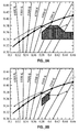
Rea and Freyssinier have proposed that lighting could be generally improved by ensuring that its CRI Ra value is at least 80 while its GAI is in a range of from 80 to 100 (i.e., 80% and 100% of an equal energy spectrum). FIG. 3 provides a plot of GAI values along the y-axis and CRI Ra values along the x-axis, with the shaded region at upper right representing a preferred combination of CRI Ra≧80 and 80≦GAI≦100. Rea and Freyssinier have proposed to designate a light source embodying CRI Ra and GAI values in the foregoing ranges as a “Class A” light source.
Characteristics including CCT, CRI Ra, GAI, CIE 1931 (x,y) coordinates, luminous efficacy (lm/W), and scotopic/photopic (S/P) ratios for eighteen different light sources are tabulated in FIG. 4A, and chromaticities for selected sources of the foregoing eighteen light sources are plotted in FIG. 4B together with the blackbody curve and the WBL (line of minimum tint). (Source: “Value Metrics for Better Lighting,” Rea, Mark S., et al., 2013, pp. 54 & 63, SPIE Press (Bellingham, Wash., US), ISBN 978-0-8194-9322-4.) Only three sources (i.e., Xenon lamp (#1.5), fluorescent F40T12 daylight lamp (#2.7), and ceramic metal halide (#2.8)) meet the Class A color designation. Although numerous solid state light sources are characterized in FIG. 4A (i.e., white LED 6500K (#1.6 and #2.10), white LED 2700K (#2.9), and blue LED 470 nm peak (#3.1)), none of these solid state light sources meet the Class A color designation. It is noted that a neodymium doped 60 W (incandescent) A-lamp (#2.2) having a CRI Ra of 78 and GAI of 65 also failed to meet the Class A color designation.
As indicated in FIG. 4A, the ability of artificial lights to accurately illuminate color objects varies enormously by type. Solid state emitters such as LEDs in combination with lumiphors create white light by mixing relatively narrow wavelength bands together with spectral gaps between peaks of LEDs and/or lumiphors. The resulting light may be under-saturated with certain colors of the spectrum or oversaturated with certain colors. One way to alleviate oversaturation with respect to certain portions of the visible spectrum and thereby improve CRI includes notch filtering of LED lighting systems with an optical element (e.g., incorporating a rare earth compound such as neodymium oxide, or a color pigment) that filters light emissions so that light passing through or reflected by the optical element exhibits a spectral notch, as disclosed in U.S. Patent Application Publication No. 2013/0170199 A2 entitled “LED lighting using spectral notching” (which is hereby incorporated by reference herein). Such publication discloses that CRI and GAI values of LED light sources can be improved through use of notch filtering, such as to increase CRI from 84 to 90, and to increase GAI from 50 to 58. Alternatively, careful selection of materials used in LED lighting devices may permit attainment of CRI Ra values of 90 to 95 or more—see, e.g., U.S. Pat. No. 7,213,940, which is hereby incorporated by reference.
The art continues to seek improved solid state lighting devices providing desirable illumination characteristics, as well as improved methods for making solid state devices.
SUMMARY
The present disclosure relates in various aspects to solid state (e.g., LED) lighting devices including multiple solid state light emitters arranged to produce a mixture of light having a color rendering index (CRI Ra) value of at least 80, having a gamut area index (GAI) value in a range of from 80 to 100, and x, y coordinates within a predefined region of a 1931 CIE Chromaticity diagram, e.g. including x, y coordinates defining point on or within a first polygon bounded by the following x, y coordinates: (0.38, 0.34), (0.38, 0.36), (0.40, 0.38), (0.42, 0.38), (0.44, 0.36), (0.46, 0.36), and (0.46, 0.34). In certain aspects, such a device may be arranged to produce a mixture of light having a CRI Ra value of at least 90, having a GAI value in a range of from 80 to 100, and x, y coordinates within a predefined region of a 1931 CIE Chromaticity diagram, e.g. including x, y coordinates defining point on or within a second polygon bounded by the following x, y coordinates: (0.38, 0.34), (0.38, 0.36), (0.40, 0.38), and (0.40, 0.36). In certain aspects, at least one lumiphoric material may be associated with one or more solid state light emitters. The simultaneous attainment of enhanced vividness and high CRI Ra utilizing solid state emitters (and being devoid of incandescent or other emitter types) represents a significant advance relative to the prior art as exemplified by various light-emitting sources (including solid state light sources) characterized by Rea et al. as reproduced in FIGS. 4A-4B.
In one aspect, the present disclosure relates to a lighting device comprising multiple electrically activated solid state light emitters, wherein: a combination of light exiting the lighting device that was emitted by the multiple electrically activated solid state light emitters would, in the absence of any additional light, produce a mixture of light having a color point on a 1931 CIE Chromaticity Diagram including x, y coordinates that define a point on or within a first polygon bounded by the following x, y coordinates: (0.38, 0.34), (0.38, 0.36), (0.40, 0.38), (0.42, 0.38), (0.44, 0.36), (0.46, 0.36), and (0.46, 0.34); the mixture of light has a color rendering index (CRI Ra) value of at least 80; and the mixture of light has a gamut area index (GAI) value in a range of from 80 to 100.
In another aspect, the present disclosure relates to a lighting device comprising: at least one primary solid state light emitter arranged to emit primary solid state light emitter emissions comprising a dominant wavelength in a range of from 430 nm to 480 nm; at least one lumiphor arranged to receive and be excited by at least a portion of emissions of the at least one primary solid state light emitter, and emit lumiphor emissions comprising a dominant wavelength in a range of from about 535 nm to about 585 nm; and at least one supplemental solid state light emitter arranged to generate supplemental solid state light emitter emissions comprising a dominant wavelength in a range of from 590 nm to 650 nm; wherein a combination of (A) light exiting the lighting device that was emitted by the at least one primary solid state light emitter, (B) light exiting the lighting device that was emitted by the at least one lumiphor, and (C) light exiting the lighting device that was emitted by the at least one supplemental solid state light emitter would, in the absence of any additional light, produce a mixture of light having a color point on a 1931 CIE Chromaticity Diagram including x, y coordinates that define a point on or within a first polygon bounded by the following x, y coordinates: (0.38, 0.34), (0.38, 0.36), (0.40, 0.38), (0.42, 0.38), (0.44, 0.36), (0.46, 0.36), and (0.46, 0.34); wherein the mixture of light has a color rendering index (CRI Ra) value of at least 80; and wherein the mixture of light has a gamut area index (GAI) value in a range of from 80 to 100.
In another aspect, the present disclosure relates to a method comprising illuminating an object, a space, or an environment, utilizing a solid state lighting device as described herein.
In another aspect, any of the foregoing aspects, and/or various separate aspects and features as described herein, may be combined for additional advantage. Any of the various features and elements as disclosed herein may be combined with one or more other disclosed features and elements unless indicated to the contrary herein.
Other aspects, features and embodiments of the present disclosure will be more fully apparent from the ensuing disclosure and appended claims.
BRIEF DESCRIPTION OF THE DRAWINGS
FIG. 1 is a side cross-sectional view of a first conventional light emitting diode package.
FIG. 2 is an excerpt of a CIE 1931 chromaticity diagram showing the blackbody locus and including a line of minimum tint (or “white body line”) extending between CCT values of from 2700K to 6500K.
FIG. 3 is a two dimensional plot of gamut area index (GAI) and color rendering index (CRI Ra) including a shaded region at upper right representing a preferred combination of CRI Ra≧80 and 80≦GAI≦100.
FIG. 4A is a chart including CCT, CRI Ra, GAI, CIE 1931 (x,y) coordinates, luminous efficacy (lm/W), and scotopic/photopic (S/P) ratios for eighteen different light sources.
FIG. 4B is an excerpt of a CIE 1931 chromaticity diagram showing the blackbody locus, the line of minimum tint (or “white body line”) extending between CCT values from 2700K to 6500K, and (x,y) coordinate plots for selected sources of the eighteen light sources listed in FIG. 4A.
FIG. 5A is an excerpt of a CIE 1931 chromaticity diagram showing the blackbody locus, the line of minimum tint (or “white body line”) extending between CCT values from 2700K to 6500K, periodic color temperature lines intersecting the blackbody locus, and plots of nine zones with different ranges of gamut area index (GAI) obtained by modeling a first exemplary lighting device including a blue LED (452 nm peak wavelength) arranged to stimulate emissions of a yellow (YAG 108) phosphor, in combination with an orange-red LED (619 nm dominant wavelength).
FIG. 5B is an excerpt of a CIE 1931 chromaticity diagram showing the blackbody locus, the line of minimum tint (or “white body line”) extending between CCT values from 2700K to 6500K, periodic color temperature lines intersecting the blackbody locus, and plots of ten zones with different ranges of color rendering index (CRI Ra) obtained by modeling the same lighting device according to FIG. 5A.
FIG. 6A is an excerpt of a CIE 1931 chromaticity diagram showing the blackbody locus, the line of minimum tint (or “white body line”) extending between CCT values from 2700K to 6500K, periodic color temperature lines intersecting the blackbody locus, and plots of nine zones with different ranges of gamut area index (GAI) obtained by modeling a second exemplary lighting device including a blue LED (452 nm peak wavelength) arranged to stimulate emissions of a yellow/green (LuAg) phosphor, in combination with an orange-red (619 nm dominant wavelength) LED.
FIG. 6B is an excerpt of a CIE 1931 chromaticity diagram showing the blackbody locus, the line of minimum tint (or “white body line”) extending between CCT values from 2700K to 6500K, periodic color temperature lines intersecting the blackbody locus, and plots of ten zones with different ranges of color rendering index (CRI Ra) obtained by modeling the same lighting device according to FIG. 6A.
FIG. 6C is an excerpt of a CIE 1931 chromaticity diagram showing the blackbody locus, the line of minimum tint (or “white body line”) extending between CCT values from 2700K to 6500K, periodic color temperature lines intersecting the blackbody locus, and plots of eight zones with different ranges of scotopic/photopic (S/P) ratio obtained by modeling the same lighting device according to FIGS. 6A-6B.
FIGS. 7A-7E in combination embody a table providing numerical results for modeling of 151 solid state lighting devices each including an orange or red LED (source 1 a), a yellow or yellow/green phosphor (source a), and a blue LED (source 3 a), including device number, CIE 1931 x,y coordinates of combined emissions, dominant LED wavelength (dm), correlated color temperature (cct), S/P ratio, CRI Ra, R9 color rendering, color quality scale (CQS), gamut area index (GAI), source identifiers, lumen percentage for each individual source, CIE 1931 x,y coordinates for each individual source, dominant wavelength (dm) for each individual source, and peak wavelength (pk) for each individual source.
FIG. 8A is an excerpt of a CIE 1931 chromaticity diagram showing the blackbody locus, a segmented representation (including six points) of the line of minimum tint (or “white body line”) extending between CCT values of from 2700K to 6500K, and including a shaded first polygon bounded by the following x, y coordinates: (0.38, 0.34), (0.38, 0.36), (0.40, 0.38), (0.42, 0.38), (0.44, 0.36), (0.46, 0.36), and (0.46, 0.34) including color points of the modeled solid state lighting devices represented in FIGS. 7A-7E.
FIG. 8B is an excerpt of a CIE 1931 chromaticity diagram showing the blackbody locus, a segmented representation (including six points) of the line of minimum tint (or “white body line”) extending between CCT values of from 2700K to 6500K, and including a shaded second polygon bounded by the following x, y coordinates: (0.38, 0.34), (0.38, 0.36), (0.40, 0.38), and (0.40, 0.36) including color points of selected modeled solid state lighting devices represented in FIGS. 7A-7E.
FIG. 9A is a table including numerical results for modeling of a solid state lighting device including an orange (606 nm dominant wavelength) LED, a blue (450 nm dominant wavelength) LED, and a green phosphor (P1LuGaAg 4), yielding composite emissions with a CCT of 3511K, a CRI Ra value of 80, and a GAI value of 100.
FIG. 9B is an excerpt of a CIE 1931 chromaticity diagram showing the blackbody locus, a portion of the line of minimum tint (or white body line), and the following items for the LEDs and phosphor of FIG. 9A: tie lines, gamut area, and composite color point.
FIG. 10 is a table including numerical results for modeling of a solid state lighting device including an amber (599 nm dominant wavelength) LED, a green (532 nm dominant wavelength) LED, and a blue (447 nm dominant wavelength) LED, yielding composite emissions with a CCT of 3511K, a CRI Ra value of 80, and a GAI value of 94.
FIG. 11A is a side cross-sectional schematic view of a portion of a solid state lighting device including an electrically activated solid state light emitter (e.g., LED) and at least one lumiphor dispersed in an encapsulant material disposed over the solid state light emitter.
FIG. 11B is a side cross-sectional schematic view of a portion of a solid state lighting device including an electrically activated solid state light emitter (e.g., LED) and at least one lumiphor arranged in one or more layers spatially separated from the solid state light emitter.
FIG. 11C is a side cross-sectional schematic view of a portion of a solid state lighting device including multiple electrically activated solid state light emitters (e.g., LEDs) and at least one lumiphor dispersed in an encapsulant material disposed over the multiple solid state light emitters.
FIG. 11D is a side cross-sectional schematic view of a portion of a solid state lighting device including multiple solid state light emitters (e.g., LEDs) and at least one lumiphor arranged in one or more layers spatially separated from the multiple solid state light emitters.
FIG. 11E is a side cross-sectional schematic view of a portion of a solid state lighting device including multiple solid state light emitters (e.g., LEDs), with at least one solid state light emitter having a lumiphor material individually applied or coated over at least one surface of the solid state light emitter.
FIG. 11F is a side cross-sectional schematic view of a portion of a solid state lighting device including multiple solid state light emitters (e.g., LEDs), with multiple solid state light emitters each having a lumiphor material individually applied or coated over at least one surface of the respective emitter.
FIG. 12A is a side cross-sectional schematic view of at least a portion of a solid state light emitting device including a solid state emitter chip arranged over a package mount, with a top surface of the emitter chip being covered with a wavelength conversion material.
FIG. 12B is a side cross-sectional schematic view of at least a portion of a solid state light emitting device including the device of FIG. 12A with addition of a curved (e.g., hemispherical) lens.
FIG. 12C is a side cross-sectional schematic view of at least a portion of a solid state light emitting device including a solid state emitter chip arranged over a package mount, with top and side surfaces of the emitter chip and an upper surface of the package mount being covered with a wavelength conversion material.
FIG. 12D is a side cross-sectional schematic view of at least a portion of a solid state light emitting device including the device of FIG. 12C with addition of a lens having a substantially rectangular cross-sectional shape.
FIG. 12E is a side cross-sectional schematic view of at least a portion of a solid state light emitting device including multiple solid state emitter chips arranged over a package mount, with a top surface of each emitter chip being covered with at least one wavelength conversion material.
FIG. 12F is a side cross-sectional schematic view of at least a portion of a solid state light emitting device including the device of FIG. 12E with addition of a lens having a beveled upper edge with a non-rectangular (polygonal) cross-sectional shape.
FIG. 12G is a side cross-sectional schematic view of at least a portion of a solid state light emitting device including a solid state emitter chip arranged over a package mount.
FIG. 12H is a side cross-sectional schematic view of at least a portion of a solid state light emitting device including the device of FIG. 12G with addition of a lens having a substantially rectangular cross-sectional shape, and with addition of a functional material (e.g., wavelength conversion material) arranged on a surface of the lens and spatially separated from the solid state emitter chip.
FIG. 13A is a side cross-sectional schematic view of at least a portion of a solid state light emitting device including a solid state emitter chip arranged over a package mount, with a top surface of the emitter chip being covered with a wavelength conversion material and a filtering (e.g., notch filtering) material.
FIG. 13B is a side cross-sectional schematic view of at least a portion of a solid state light emitting device including the device of FIG. 13A with addition of a curved (e.g., hemispherical) lens.
FIG. 13C is a side cross-sectional schematic view of at least a portion of a solid state light emitting device including a solid state emitter chip arranged over a package mount, with top and side surfaces of the emitter chip and an upper surface of the package mount being covered with a wavelength conversion material and a filtering material.
FIG. 13D is a side cross-sectional schematic view of at least a portion of a solid state light emitting device including the device of FIG. 13C with addition of a lens having a substantially rectangular cross-sectional shape.
FIG. 13E is a side cross-sectional schematic view of at least a portion of a solid state light emitting device including a solid state emitter chip arranged over a package mount, with a top surface of the emitter chip being covered with a wavelength conversion material and a filtering material, and with side surfaces of the emitter chip and an upper surface of the package mount being covered with a filtering material.
FIG. 13F is a side cross-sectional schematic view of at least a portion of a solid state light emitting device including the device of FIG. 13E with addition of a lens having a beveled upper edge with a non-rectangular (polygonal) cross-sectional shape.
FIG. 14 is a side cross-sectional view of at least a portion of a solid state lighting emitting device including multiple solid state emitter chips coated with multiple functional materials and arranged under a hemispherical optical element.
FIG. 15 is a perspective view of at least a portion of a solid state emitter package including multiple solid state emitter chips coated with one or more functional materials, with the chips coupled to electrical traces via wirebonds and arranged under a hemispherical optical element.
FIG. 16 is a side cross-sectional view of a first light bulb arranged to incorporate multiple solid state emitter chips as disclosed herein.
FIG. 17 is a side cross-sectional view of a second, reflector-type light bulb arranged to incorporate at least one emitter chip as disclosed herein.
FIG. 18 is a side cross-sectional view of a third light bulb arranged to incorporate multiple solid state emitter chips as disclosed herein in a tower-type configuration.
FIG. 19A is an upper perspective view of a troffer-type light fixture arranged to incorporate multiple solid state emitter chips as disclosed herein.
FIG. 19B is a side cross-sectional view of a portion of the light fixture of FIG. 19A.
FIG. 20 is a simplified plan view of a light emitting apparatus including multiple LED components and at least one control circuit.
FIG. 21 is a plot of radiant flux versus wavelength for a spectral output of a solid state light emitting device with superimposed notch filtered spectral output.
FIG. 22 depicts spectral transmittance versus wavelength for an illustrative color pigment material.
DETAILED DESCRIPTION
As noted previously, the art continues to seek solid state lighting devices providing desirable illumination characteristics. Various embodiments disclosed herein include solid state (e.g., LED) lighting devices including multiple solid state light emitters arranged to produce a mixture of light having a color rendering index (CRI Ra) value of at least 80, having a gamut area index (GAI) value in a range of from 80 to 100, and x, y coordinates within a predefined region of a 1931 CIE Chromaticity diagram, e.g. including x, y coordinates defining point on or within a first polygon bounded by the following x, y coordinates: (0.38, 0.34), (0.38, 0.36), (0.40, 0.38), (0.42, 0.38), (0.44, 0.36), (0.46, 0.36), and (0.46, 0.34), or within a second polygon bounded by the following x, y coordinates: (0.38, 0.34), (0.38, 0.36), (0.40, 0.38), and (0.40, 0.36), wherein in the case of the second polygon the CRI Ra value may be in a range of at least 90. Each of the foregoing polygons is below the blackbody locus and includes CCT values below 4000K. The foregoing devices simultaneously provide enhanced vividness and sufficiently high CRI Ra to be used for general illumination. In certain embodiments, the plurality of solid state light emitters may include a primary solid state light emitter arranged to generate emissions comprising a dominant wavelength in a range of from 430 nm to 480 nm, and at least one supplemental solid state light emitter arranged to generate supplemental solid state light emitter emissions comprising a dominant wavelength in a range of from 590 nm to 650 nm; wherein at least one lumiphor is arranged to receive and be excited by at least a portion of emissions of the at least one primary solid state light emitter and responsively emit lumiphor emissions comprising a dominant wavelength in a range of from about 535 nm to about 585 nm (or in a range of from 545 nm to 585 nm in certain embodiments).
Unless otherwise defined, terms used herein should be construed to have the same meaning as commonly understood by one of ordinary skill in the art to which the present disclosure belongs. It will be further understood that terms used herein should be interpreted as having a meaning that is consistent with their meaning in the context of this specification and the relevant art, and should not be interpreted in an idealized or overly formal sense unless expressly so defined herein.
It will be understood that, although the terms first, second, etc. may be used herein to describe various elements, these elements should not be limited by these terms. These terms are only used to distinguish one element from another. For example, a first element could be termed a second element, and, similarly, a second element could be termed a first element, without departing from the scope of the present disclosure. As used herein, the term “and/or” includes any and all combinations of one or more of the associated listed items.
Embodiments of the present disclosure are described herein with reference to cross-sectional, perspective, elevation, and/or plan view illustrations that are schematic illustrations of idealized embodiments of the present disclosure. Variations from the shapes of the illustrations as a result, for example, of manufacturing techniques and/or tolerances, are to be expected, such that embodiments of the present disclosure should not be construed as limited to particular shapes illustrated herein. The present disclosure may be embodied in different forms and should not be construed as limited to the specific embodiments set forth herein. In the drawings, the size and relative sizes of layers and regions may be exaggerated for clarity. In certain drawings, conventional features inherent to LED devices known in the art but not essential to the understanding of the present disclosure have been omitted to facilitate ease of explanation of the inventive subject matter.
Unless the absence of one or more elements is specifically recited, the terms “comprising,” “including,” and “having” as used herein should be interpreted as open-ended terms that do not preclude the presence of one or more elements.
It will be understood that when an element such as a layer, region, or substrate is referred to as being “on” another element, it can be directly on the other element or intervening elements may be present. Moreover, relative terms such as “on”, “above”, “upper”, “top”, “lower”, or “bottom” may be used herein to describe a relationship between one structure or portion to another structure or portion as illustrated in the figures, but it should be understood that such relative terms are intended to encompass different orientations of the device in addition to the orientation depicted in the figures. For example, if the device in the figures is turned over, structure or portion described as “above” other structures or portions would now be oriented “below” the other structures or portions.
The terms “solid state light emitter” or “solid state emitter” (which may be qualified as being “electrically activated”) may include a light emitting diode, laser diode, organic light emitting diode, and/or other semiconductor device which includes one or more semiconductor layers, which may include silicon, silicon carbide, gallium nitride and/or other semiconductor materials, a substrate which may include sapphire, silicon, silicon carbide and/or other microelectronic substrates, and one or more contact layers which may include metal and/or other conductive materials.
Solid state light emitting devices according to embodiments of the present disclosure may include, but are not limited to, III-V nitride based LED chips or laser chips fabricated on a silicon, silicon carbide, sapphire, or III-V nitride growth substrate, including (for example) devices manufactured and sold by Cree, Inc. of Durham, N.C. Such LEDs and/or lasers may optionally be configured to operate such that light emission occurs through the substrate in a so-called “flip chip” orientation. Such LED and/or laser chips may also be devoid of growth substrates (e.g., following growth substrate removal).
LED chips useable with lighting devices as disclosed herein may include horizontal devices (with both electrical contacts on a same side of the LED) and/or vertical devices (with electrical contacts on opposite sides of the LED). A horizontal device (with or without the growth substrate), for example, may be flip chip bonded (e.g., using solder) to a carrier substrate or printed circuit board (PCB), or wire bonded. A vertical device (without or without the growth substrate) may have a first terminal solder bonded to a carrier substrate, mounting pad, or printed circuit board (PCB), and have a second terminal wire bonded to the carrier substrate, electrical element, or PCB. Although certain embodiments shown in the figures may be appropriate for use with vertical LEDs, it is to be appreciated that the present disclosure is not so limited, such that any combination of one or more of the following LED configurations may be used in a single solid state light emitting device: horizontal LED chips, horizontal flip LED chips, vertical LED chips, vertical flip LED chips, and/or combinations thereof, with conventional or reverse polarity. Examples of vertical and horizontal LED chip structures are discussed by way of example in U.S. Publication No. 2008/0258130 to Bergmann et al. and in U.S. Pat. No. 7,791,061 to Edmond et al. which are hereby incorporated by reference herein.
Solid state light emitters may be used individually or in groups to emit one or more beams to stimulate emissions of one or more lumiphoric materials (e.g., phosphors, scintillators, lumiphoric inks, quantum dots, day glow tapes, etc.) to generate light at one or more peak wavelength, or of at least one desired perceived color (including combinations of colors that may be perceived as white). Lumiphoric materials may be provided in the form of particles, films, or sheets.
Inclusion of lumiphoric (also called ‘luminescent’) materials in lighting devices as described herein may be accomplished by any suitable means, including: direct coating on solid state emitters, dispersal in encapsulant materials arranged to cover solid state emitters; coating on lumiphor support elements (e.g., by powder coating, inkjet printing, or the like); incorporation into diffusers or lenses; and the like. Examples of lumiphoric materials are disclosed, for example, in U.S. Pat. No. 6,600,175, U.S. Patent Application Publication No. 2009/0184616, and U.S. Patent Application Publication No. 2012/0306355, and methods for coating light emitting elements with phosphors are disclosed in U.S. Patent Application Publication No. 2008/0179611, with the foregoing publications being incorporated by reference. Other materials, such as light scattering elements (e.g., particles) and/or index matching materials, may be associated with a lumiphoric material-containing element or surface. One or more lumiphoric materials useable in devices as described herein may be down-converting or up-converting, or can include a combination of both types.
In certain embodiments, at least one lumiphoric material may be spatially segregated (“remote”) from and arranged to receive emissions from at least one electrically activated solid state emitter, with such spatial separation reducing thermal coupling between a solid state emitter and lumiphoric material. In certain embodiments, a spatially segregated lumiphor may be arranged to fully cover one or more electrically activated emitters of a lighting device. In certain embodiments, a spatially segregated lumiphor may be arranged to cover only a portion or subset of one or more emitters electrically activated emitters.
In certain embodiments, at least one lumiphoric material may be arranged with a substantially constant thickness and/or concentration relative to different electrically activated emitters. In certain embodiments, one or more lumiphoric materials may be arranged with presence, thickness, and/or concentration that vary relative to different emitters. Multiple lumiphors (e.g., lumiphors of different compositions) may be applied with different concentrations or thicknesses relative to different electrically activated emitters. In one embodiment, lumiphor presence, composition, thickness and/or concentration may vary relative to multiple electrically activated emitters. In certain embodiment, at least one lumiphoric material may be applied to a solid state emitter or a lumiphoric material support surface by patterning, such may be aided by one or more masks.
Various substrates may be used as mounting elements on which, in which, or over which multiple solid state light emitters (e.g., emitter chips) may be arranged or supported (e.g., mounted). Exemplary substrates include printed circuit boards (including but not limited to metal core printed circuit boards, flexible circuit boards, dielectric laminates, and the like) having electrical traces arranged on one or multiple surfaces thereof. A substrate, mounting plate, or other support element may include a printed circuit board (PCB), a metal core printed circuit board (MCPCB), a flexible printed circuit board, a dielectric laminate (e.g., FR-4 boards as known in the art) or any suitable substrate for mounting LED chips and/or LED packages. In certain embodiments, at least a portion of a substrate may include a dielectric material to provide desired electrical isolation between electrical traces or components of multiple LED sets. In certain embodiments, a substrate can comprise ceramic such as alumina, aluminum nitride, silicon carbide, or a polymeric material such as polyimide, polyester, etc. In certain embodiments, a substrate can comprise a flexible circuit board or a circuit board with plastically deformable portions to allow the substrate to take a non-planar (e.g., bent) or curved shape allowing for directional light emission with LED chips of one or more LED components also being arranged in a non-planar manner.
In certain embodiments, one or more LED components can include one or more “chip-on-board” (COB) LED chips and/or packaged LED chips that can be electrically coupled or connected in series or parallel with one another and mounted on a portion of a substrate. In certain embodiments, COB LED chips can be mounted directly on portions of substrate without the need for additional packaging.
Certain embodiments may involve use of solid state emitter packages. A solid state emitter package may include at least one solid state emitter chip (more preferably multiple solid state emitter chips) that is enclosed with packaging elements to provide environmental protection, mechanical protection, color selection, and/or light focusing utility, as well as electrical leads, contacts, and/or traces enabling electrical connection to an external circuit. One or more emitter chips may be arranged to stimulate one or more lumiphoric materials, which may be coated on, arranged over, or otherwise disposed in light receiving relationship to one or more solid state emitters. At least one lumiphoric material may be arranged to receive emissions of at least some emitters of a plurality of solid state light emitters and responsively emit lumiphor emissions. A lens and/or encapsulant material, optionally including lumiphoric material, may be disposed over solid state emitters, lumiphoric materials, and/or lumiphor-containing layers in a solid state emitter package.
In certain embodiments, a light emitting apparatus as disclosed herein (whether or not including one or more LED packages) may include at least one of the following items arranged to receive light from multiple LEDs: a single leadframe arranged to conduct electrical power to the plurality of electrically activated solid state light emitters; a single reflector arranged to reflect at least a portion of light emanating from the plurality of electrically activated solid state light emitters; a single submount or mounting element supporting the plurality of electrically activated solid state light emitters; a single lens arranged to transmit at least a portion of light emanating from the plurality of electrically activated solid state light emitters; and a single diffuser arranged to diffuse at least a portion of light emanating from the plurality of electrically activated solid state light emitters. In certain embodiments, a light emitting apparatus including multiple LEDs may include at least one of the following items arranged to receive light from multiple LEDs: multiple lenses; multiple optical elements; and multiple reflectors. Examples of optical elements include, but are not limited to elements arranged to affect light mixing, focusing, collimation, dispersion, and/or beam shaping.
In certain embodiments, a package including multiple solid state emitters may include multiple die attach pads, with a single die attach pad supporting each separately controllable solid state emitter or each separately controllable group of solid state emitters. A package including multiple solid state emitters may include a single lens (e.g., a molded lens) arranged to transmit at least a portion of light emanating from each solid state emitter. In certain embodiments, a molded lens may be arranged in direct contact with LED chips, die attach pads, other electrical elements, and/or exposed insulating material along a top surface of a substrate comprising insulating material. In certain embodiments, a lens may be textured or faceted to improve light extraction, and/or a lens may contain or have coated thereon various materials such as lumiphors and/or scattering particles.
In certain embodiments, a package may include a molded lens arranged to transmit light emitted by multiple LEDs. As known in the art, a mold including one or more cavities can be arranged over a substrate (or a panel of substrate material, from which multiple substrates may be singulated by sawing or other means) and LED chips arranged thereon, with the mold comprising a lens material and/or encapsulant in liquid form. In certain embodiments, a lens may be formed of liquid curable silicone, and LED chips may be embedded in liquid silicone, which is subsequently cured to form one or more lenses. Alternatively, a lens may be pre-molded and then affixed (e.g., with adhesives, thermal bonding, or any other suitable joining method) to a subassembly including a substrate to which or over which with multiple LED chips are mounted.
In certain embodiments, a solid state lighting device (e.g., package) may include a reflector cup defining a cavity, at least one solid state emitter arranged within the cavity, and encapsulant material arranged within the cavity. In certain embodiments, at least one solid state emitter may be arranged over a substrate and at least partially surrounded by a boundary wall (optionally embodying at least one dispensed dam material laterally spaced from the emitter(s), with an encapsulant material arranged over the emitter(s) and in contact with the at least one boundary wall).
Various devices disclosed herein may include multiple solid state emitters (e.g., LEDs) of the same or different dominant colors, or of the same or different peak wavelengths. In certain embodiments, a solid state light emitting device may include at least three colors such as red, green, and blue emitters, which may include solid state light emitters devoid of phosphors, or may include phosphors (e.g., in combination with UV and/or blue emitters) to generate one or more of the red, green, and blue colors. Other combinations of output colors may be provided. In certain embodiments, a solid state light emitting device may include at least two colors.
The expressions “lighting device,” “light emitting device,” and “light emitting apparatus” as used herein are not limited, except that such elements are capable of emitting light. That is, a lighting device or light emitting apparatus can be a device which illuminates an area or volume, e.g., a structure, a swimming pool or spa, a room, a warehouse, an indicator, a road, a parking lot, a vehicle, signage, e.g., road signs, a billboard, a ship, a toy, a mirror, a vessel, an electronic device, a boat, an aircraft, a stadium, a computer, a remote audio device, a remote video device, a cell phone, a tree, a window, an LCD display, a cave, a tunnel, a yard, a lamppost, or a device or array of devices that illuminate an enclosure, or a device that is used for edge or back-lighting (e.g., backlight poster, signage, LCD displays), light bulbs, bulb replacements (e.g., for replacing AC incandescent lights, low voltage lights, fluorescent lights, etc.), outdoor lighting, street lighting, security lighting, exterior residential lighting (wall mounts, post/column mounts), ceiling fixtures/wall sconces, under cabinet lighting, lamps (floor and/or table and/or desk), landscape lighting, track lighting, task lighting, specialty lighting, ceiling fan lighting, archival/art display lighting, high vibration/impact lighting-work lights, etc., mirrors/vanity lighting, or any other light emitting devices. In certain embodiments, lighting devices or light emitting apparatuses as disclosed herein may be self-ballasted. In certain embodiments, a light emitting apparatus may be embodied in a light fixture.
In preferred embodiments, a solid state lighting device is devoid of any incandescent light emitting element. In certain embodiments, a solid state lighting device lacks any “unconverted” blue-emitting solid state emitter not arranged to stimulate emissions of a lumiphoric material.
The inventive subject matter further relates in certain embodiments to an illuminated enclosure (the volume of which can be illuminated uniformly or non-uniformly), comprising an enclosed space and at least one lighting device or light emitting apparatus as disclosed herein, wherein at least one lighting device or light emitting apparatus illuminates at least a portion of the enclosure (uniformly or non-uniformly). The inventive subject matter further relates to an illuminated area, comprising at least one item, e.g., selected from among the group consisting of a structure, a swimming pool or spa, a room, a warehouse, an indicator, a road, a parking lot, a vehicle, signage, e.g., road signs, a billboard, a ship, a toy, a mirror, a vessel, an electronic device, a boat, an aircraft, a stadium, a computer, a remote audio device, a remote video device, a cell phone, a tree, a window, a LCD display, a cave, a tunnel, a yard, a lamppost, etc., having mounted therein or thereon at least one lighting device or light emitting apparatus as described herein. Methods include illuminating an object, a space, or an environment, utilizing one or more lighting devices or light emitting apparatuses as disclosed herein. In certain embodiments, a lighting apparatus as disclosed herein includes multiple LED components arranged in an array (e.g., a two-dimensional array).
In certain embodiments, a color rendering index (CRI Ra) value of at least 75, or preferably at least 80, or in one of the following ranges: from 75 to 95, from 75 to 90, from 80 to 95, from 85 to 95, or from 80 to 90 may be attained in combination with GAI in a range of from 80 to 100 utilizing lighting devices as disclosed herein.
In certain embodiments, lighting devices as disclosed herein may provide emissions exhibiting enhanced vividness in combination with relatively high CRI Ra (e.g., according to one or more threshold ranges for GAI and CRI Ra recited herein) without use of any notch filtering material arranged to at least partially inhibit transmission of light. A notch filtering material when arranged on or in a light transmissive surface of a lighting device will inherently entail at least some attenuation of light and concomitant reduction of luminous efficacy. Presence of notch filtering material in a lighting device may also increase need for heat dissipating structures (e.g., heatsinks) since notch filtering material is subjected to being heated by absorbed light energy. As a result, providing a lighting device that is devoid of notch filtering material may avoid reduction of luminous efficacy, and may reduce need for heat dissipating structures, relative to a lighting device incorporating a notch filtering material.
In other embodiments, lighting devices as disclosed herein may include or have associated therewith one or more notch filtering materials, such as to enhance GAI and/or CRI Ra.
The term “notch filtering material” refers to a material that affects passage of light to cause light exiting the material to exhibit a spectral notch. A spectral notch is a portion of the color spectrum where the light is attenuated, thus forming a “notch” when light intensity is plotted against wavelength. Examples of notch filtering materials include rare earth and lanthanide materials, such as lanthanum, cerium, praseodymium, neodymium, promethium, samarium, europium, gadolinium, terbium, dysprosium, holmium, erbium, thulium, ytterbium, lutetium, scandium, and yttrium, as well as oxides thereof (e.g., neodymium oxide). Different rare earth compounds may exhibit notch filtering characteristics of different wavelength ranges. For example, neodymium (or oxide thereof) when used as a filtering material may produce a spectral notch in the yellow range, whereas erbium (or oxide thereof) when used as a filtering material may produce a spectral notch in the cyan range. Additional notch filtering materials include color pigments. As with the use of rare earth compounds, the use of color pigments can impart notch filtering properties in either transmissive or reflective applications. In many instances, color pigments may provide softer spectral notch (with more gradually sloping wavelength attenuation) characteristics relative to other notch filtering materials. One example of a color pigment includes an ultramarine pigment based on CoAl2O4, providing peak attenuation at a wavelength of about 580 nm. A cobalt blue pigment of similar composition could also be used. Other color pigments based on CuSO4 or NiCl2 can also be used. A variety of natural and synthetic pigments are available and could be used as notch filtering materials according to certain embodiments disclosed herein. Notch filters may also be fabricated by depositing one or more dielectric layers (e.g., to form dielectric stacks) on substrates, such as filters commercially available from Thorlabs, Inc. (Newton, N.J., US) having the following center wavelengths (CWL) and full width at half maximum (FWHM) characteristics: CWL=488 nm, FWHM=15 nm; CWL=514 nm, FWHM=17 nm; CWL=533 nm, FWHM=17 nm; CWL=561 nm, FWHM=18 nm; CWL=594 nm, FWHM=23 nm; 633 nm, FWHM=25 nm; and CWL=658 nm, FWHM=26 nm.
In certain embodiments utilizing one or more notch filtering materials, a spectral notch provided by at least one filtering material may have a full width in a range of less than or equal to 40 nm, or less than or equal to 35 nm, or less than or equal to 30 nm, or less than or equal to 25 nm, or less than or equal to 20 nm, in each case corresponding to a half maximum relative reduction in light transmission. In certain embodiments utilizing one or more notch filtering materials, at least one filtering material may be arranged to filter light within (or overlapping) the yellow-green range or yellow range, such as to provide peak attenuation in a range of from 550 nm to 590 nm, or from 570 nm to 590 nm.
In embodiments utilizing notch filtering materials, a resulting notch filtered solid state lighting device may include emissions having a gamut area index (GAI) value in a range of from 80 to 100, preferably in combination with a color rendering index (CRI Ra) value of at least 75, more preferably at least 80, or more preferably at least 90. A notch filtering material according to certain embodiments may be arranged to provide a spectral notch having a full width of less than 40 nm corresponding to a half maximum relative reduction in light transmission. In certain embodiments, the notch filtering material may serve to attenuate intensity of emissions output by the solid state lighting device by at least 10%, or at least 20%, or at least 30%, or at least 40%, or at least 50%.
In embodiments utilizing notch filtering materials, such materials may be provided as microparticles or nanoparticles of any desired size, size distribution, and geometric shape. In certain embodiments, multiple notch filtering materials may be mixed and incorporated in a carrier material or binder, or multiple notch filtering materials may otherwise be used in combination (e.g., in sequential layers, with or without a binding medium) to provide multiple spectral notches. In certain embodiments, notch filtering materials may be arranged in or on an at least partially light-transmissive optical element or enclosure, which may serve as a lens and/or diffuser. Examples of desirable materials for carriers, binding media, enclosures, and/or optical elements include (but are not limited to) silicone, resin, epoxy, thermoplastic polycondensate, polymeric materials, and glass. In certain embodiments, such materials may be molded and/or cured together with at least one notch filtering material. In certain embodiments, a lighting device may include one or more transmissive optical elements and/or reflective optical elements incorporating at least one notch filtering material. For example, a so-called “troffer” style ceiling fixture may include a reflector that serves as an optical element, and may additionally include optical elements such as glass plates or lenses.
In certain embodiments utilizing notch filtering materials, at least one filtering material (e.g., notch filtering material) may be arranged with a substantially constant thickness and/or concentration relative to different electrically activated emitters (e.g., solid state emitters such as LEDs). In certain embodiments, one or more filtering materials may be arranged on or over at least one solid state emitter (optionally with an intervening lumiphoric material) with presence, composition, thickness, and/or concentration that vary relative to different emitters. Multiple filtering materials (e.g., filtering materials of different compositions and arranged to provide spectral notches at different wavelengths) may be applied to one or more electrically activated emitters. In certain embodiments, at least one filtering material may be applied over one or more solid state light emitters, or over a support surface (e.g., lens, diffuser, reflector, etc.) utilizing a patterning technique, such may be aided by one or more masks. In certain embodiments, one or more notch filtering materials may be integrated with or arranged in contact with one or more portions of a solid state emitter package.
In certain embodiments utilizing notch filtering materials, one or more notch filtering materials may be mixed with one or more other functional materials (e.g., lumiphoric materials, scattering materials, and the like) and preferably incorporated into a binder or other carrier medium. In certain embodiments, at least one filtering material may be arranged in or on a carrier arranged on or over a plurality of solid state light emitters.
In certain embodiments utilizing notch filtering materials, notch filtering materials may be arranged in or on a reflector, which may be either specularly reflective or diffusively reflective. Any suitable reflective material in the art may be used, including (but not limited to) MCPET (foamed white polyethylene terephthalate), and surfaces metalized with one or more metals such as (but not limited to) silver (e.g., a silvered surface). MCPET manufactured by Otsuka Chemical Co. Ltd. (Osaka, Japan) is a diffuse white reflector that has a total reflectivity of 99% or more, a diffuse reflectivity of 96% or more, and a shape holding temperature of at least about 160° C. A preferred light-reflective material would be at least about 90% reflective, more preferably at least about 95% reflective, and still more preferably at least about 98-99% reflective of light of a desired wavelength range, such as one or more of visible light, ultraviolet light, and/or infrared light, or subsets thereof. In certain embodiments, at least one notch filtering material may be deposited on a surface of a reflector by spray coating, spin coating, sputtering, dipping, or rolling. Additionally deposition methods that may be used include electrostatic deposition and electrophoretic deposition. In certain embodiments, at least one notch filtering may be incorporated into a surface of a reflector via methods such as molding or sintering.
In certain embodiments utilizing notch filtering materials, one or more notch filtering materials may be coated or otherwise arranged on, over, or against at least one surface of one or more one solid state emitter chips. In certain embodiments, one or more notch filtering materials may be coated or otherwise arranged on, over, or against at least one surface of at least one lumiphoric material, wherein the at least one lumiphoric material may be arranged in direct contact with at least one surface of a solid state emitter chip, or may be arranged remotely from (i.e., spatially segregated from) at least one surface of a solid state emitter chip. In certain embodiments, one or more notch filtering materials may be conformally coated on the surface of at least one solid state emitter chip and/or lumiphoric material, wherein conformal coating in this regard refers to a coating that follows the shape and contour of at least one surface (or preferably multiple surfaces) of a chip with a substantially uniform thickness.
As will be recognized by one skilled in the art, parameters such as the type or composition of carrier or binding medium; the thickness, concentration, particle size, and particle size distribution of notch filtering material(s); and the presence, amount, and type of other trace substances accompanying one or notch filtering elements, may be adjusted to provide one or more spectral notches of desired width and/or depth.
In certain embodiments, a lighting device may include multiple electrically activated solid state light emitters, wherein: a combination of light exiting the lighting device that was emitted by the multiple electrically activated solid state light emitters would, in the absence of any additional light, produce a mixture of light having a color point on a 1931 CIE Chromaticity Diagram including x, y coordinates that define a point on or within a first polygon bounded by the following x, y coordinates: (0.38, 0.34), (0.38, 0.36), (0.40, 0.38), (0.42, 0.38), (0.44, 0.36), (0.46, 0.36), and (0.46, 0.34); the mixture of light has a color rendering index (CRI Ra) value of at least 80; and the mixture of light has a gamut area index (GAI) value in a range of from 80 to 100. In certain embodiments, the combination (in the absence of any additional light) would produce a mixture of light having a color point on a 1931 CIE Chromaticity Diagram including x, y coordinates that define a point on or within a second polygon bounded by the following x, y coordinates: (0.38, 0.34), (0.38, 0.36), (0.40, 0.38), and (0.40, 0.36), with the mixture of light having a color rendering index (CRI Ra) value of at least 90. The foregoing mixture(s) of light may preferably embody luminous efficacy of preferably at least 60 lumens per watt, more preferably at least 80 lumens per watt, and more preferably still at least 100 lumens per watt. In certain embodiments, each electrically activated solid state light emitter of the multiple electrically activated solid state light emitters is electrically connected to a first power line. In certain embodiments, at least one emitter (or group of emitters) of the multiple electrically activated solid state light emitters is independently controlled relative to at least one other emitter (or other group of emitters) of the multiple electrically activated solid state light emitters. In certain embodiments, at least one electrically activated solid state emitter of the multiple electrically activated solid state light emitters includes at least one light emitting diode (LED) chip and a lumiphoric material arranged to receive at least a portion of emissions of the at least one LED chip (wherein the lumiphoric material optionally may be spatially segregated (i.e., remotely located) from the solid state light emitters) and responsively emit lumiphor emissions. In other embodiments, the lumiphoric material may be arranged in a coating on at least one solid state emitter. In certain embodiments, the lighting device may be devoid of any non-lumiphor-converted blue solid state emitter (i.e., the lighting device may be devoid of any electrically activated solid state light emitter arranged to generate emissions that have dominant wavelength in a range of from 430 nm to 480 nm and that exit the lighting device without passage through a layer or region comprising a lumiphoric material). In certain embodiments, the lighting device may be devoid of any incandescent light emitter. In certain embodiments, the lighting device may comprise or be embodied in a solid state emitter package as disclosed herein. In certain embodiments, the lighting device may be devoid of any notch filtering material arranged to receive emissions of any one or more solid state light emitters of the multiple electrically activated solid state light emitters. In alternative embodiments, the lighting device may including notch filtering material arranged in a light path between (i) at least one electrically activated solid state emitter of the multiple electrically activated solid state emitters and (ii) at least one light output surface of the lighting device, wherein the notch filtering material is arranged to receive at least a portion emissions of the at least one electrically activated solid state emitter and filter the received emissions to exhibit a spectral notch. In certain embodiments, a light bulb or lighting fixture may include the foregoing lighting device(s). In certain embodiments, a method comprises illuminating an object, a space, or an environment, utilizing the foregoing lighting device(s).
In certain embodiments, a lighting device may include at least one primary solid state light emitter arranged to generate emissions comprising a dominant wavelength in a range of from 430 nm to 480 nm (or in a range of from 440 nm to 460 nm), at least one supplemental solid state light emitter arranged to generate supplemental solid state light emitter emissions comprising a dominant wavelength in a range of from 590 nm to 650 nm (or in a range of from 600 nm to 630 nm), and at least one lumiphor arranged to receive and be excited by at least a portion of emissions of the at least one primary solid state light emitter and responsively emit lumiphor emissions comprising a dominant wavelength in a range of from about 535 nm to about 585 nm, wherein a combination of (A) light exiting the lighting device that was emitted by the at least one primary solid state light emitter, (B) light exiting the lighting device that was emitted by the at least one lumiphor, and (C) light exiting the lighting device that was emitted by the at least one supplemental solid state light emitter would, in the absence of any additional light, produce a mixture of light having a color point on a 1931 CIE Chromaticity Diagram including x, y coordinates that define a point on or within a first polygon bounded by the following x, y coordinates: (0.38, 0.34), (0.38, 0.36), (0.40, 0.38), (0.42, 0.38), (0.44, 0.36), (0.46, 0.36), and (0.46, 0.34); the mixture of light has a color rendering index (CRI Ra) value of preferably at least 80; and the mixture of light has a gamut area index (GAI) value in a range of from 80 to 100. In certain embodiments, the combination (in the absence of any additional light) would produce a mixture of light having a color point on a 1931 CIE Chromaticity Diagram including x, y coordinates that define a point on or within a second polygon bounded by the following x, y coordinates: (0.38, 0.34), (0.38, 0.36), (0.40, 0.38), and (0.40, 0.36), with the mixture of light having a color rendering index (CRI Ra) value of at least 90. The foregoing mixture(s) of light may preferably embody luminous efficacy of preferably at least 60 lumens per watt, more preferably at least 80 lumens per watt, and more preferably still at least 100 lumens per watt. In certain embodiments, the at least one primary solid state light emitter includes a plurality of primary solid state light emitters, and the at least one secondary solid state light emitter comprises a plurality of secondary solid state light emitters; such a device may optionally include multiple clusters of solid state light emitters, wherein each cluster includes at least one primary solid state light emitter and at least one supplemental solid state light emitter. In certain embodiments, a light bulb or lighting fixture may include the foregoing lighting device(s). In certain embodiments, a method comprises illuminating an object, a space, or an environment, utilizing the foregoing lighting device(s).
In certain embodiments, each of the at least one primary and the at least one secondary electrically activated solid state light emitter may be electrically connected to a first power line. In certain embodiments, the at least one primary emitter is independently controlled relative to the at least one secondary emitter. In certain embodiments, the at least one lumiphoric material may be spatially segregated (i.e., remotely located) from the at least one primary solid state light emitter. In other embodiments, the lumiphoric material may be arranged in a coating on at least one primary solid state emitter. In certain embodiments, the lighting device may be devoid of any non-lumiphor-converted blue solid state emitter (i.e., the lighting device may be devoid of any electrically activated solid state light emitter arranged to generate emissions that have dominant wavelength in a range of from 430 nm to 480 nm and that exit the lighting device without passage through a layer or region comprising a lumiphoric material). In certain embodiments, the lighting device may comprise or be embodied in a solid state emitter package as disclosed herein. In certain embodiments, the lighting device may be devoid of any incandescent light emitter. In certain embodiments, the lighting device may be devoid of any notch filtering material arranged to receive emissions of any of the primary and supplemental solid state emitters. In alternative embodiments, the lighting device may including notch filtering material arranged in a light path between (i) any of the primary and supplemental solid state emitters, and (ii) at least one light output surface of the lighting device, wherein the notch filtering material is arranged to receive at least a portion emissions of the solid state emitters and/or lumiphor emissions and filter the received emissions to exhibit a spectral notch.
Various features and embodiments of the present disclosure are described with reference to the accompanying figures. As noted above, certain embodiments are devoid of notch filtering material. In other embodiments, one or more notch filtering materials may be provided.
FIGS. 5A-5B graphically illustrate GAI and CRI Ra values, respectively, obtained by modeling a first exemplary lighting device including a blue LED (452 nm peak wavelength) arranged to stimulate emissions of a yellow (YAG 108) phosphor, in combination with an orange-red LED (619 nm dominant wavelength), with the lighting device being devoid of any notch filtering material. In particular, FIG. 5A is an excerpt of a CIE 1931 chromaticity diagram showing the blackbody locus, the line of minimum tint (also termed “white body line” or “WBL” herein) extending between CCT values from 2700K to 6500K, periodic color temperature lines intersecting the blackbody locus, and plots of nine zones (i.e., zones I to IX) with different ranges of gamut area index (GAI) obtained such modeling. In FIG. 5A, zone V is of particular interest since it corresponds to a preferred range of GAI values from 80 to 100, and further encompasses a portion of the white body line (WBL) in a range of certain desirable CCT values below 4000K (with such region of the WBL being below the blackbody locus). FIG. 5B is an excerpt of a CIE 1931 chromaticity diagram showing the blackbody locus, the line of minimum tint (or “white body line”) extending between CCT values from 2700K to 6500K, periodic color temperature lines intersecting the blackbody locus, and plots of ten zones (i.e., zones I to X) with different ranges of color rendering index (CRI Ra) obtained by modeling the same lighting device according to FIG. 5A. In FIG. 5B, zone I (corresponding to CRI Ra values of 90 to 100) and zone II (corresponding to CRI Ra values of from 80 to 90) are of particular interest since the recited ranges are suitable for general illumination and encompass the white body line (WBL) in a range of desirable CCT values below 4000K (with such region of the WBL being below the blackbody locus). FIGS. 5A-5B in combination show that a first solid state lighting device including a phosphor-converted blue primary LED and a supplemental orange/red LED can simultaneously achieve the preferred combination of CRI Ra 80 (or CRI Ra≧90) and 80≦GAI≦100. Such condition is achieved in combination with high luminous efficacy (e.g., at least 60 LPW, at least 80 LPW, at least 100 LPW (or up to 120 LPW or more) without use of notch filtering material.
FIGS. 6A-6C graphically illustrate GAI, CRI Ra, and S/P ratio values, respectively, obtained by modeling a second exemplary device including a blue LED (452 nm peak wavelength) arranged to stimulate emissions of a yellow/green (LuAg) phosphor, in combination with an orange-red (619 nm dominant wavelength) LED. In particular, FIG. 6A is a an excerpt of a CIE 1931 chromaticity diagram showing the blackbody locus, the line of minimum tint (or “white body line”) extending between CCT values from 2700K to 6500K, periodic color temperature lines intersecting the blackbody locus, and plots of nine zones with different ranges of gamut area index (GAI) obtained by such modeling. In FIG. 6A, zone V is of particular interest since it corresponds to a preferred range of GAI values from 80 to 100, and further encompasses the majority of the white body line (WBL) (including numerous values in a range of certain desirable CCT values below 4000K below the blackbody locus. FIG. 6B is an excerpt of a CIE 1931 chromaticity diagram showing the blackbody locus, the line of minimum tint (or “white body line”) extending between CCT values from 2700K to 6500K, periodic color temperature lines intersecting the blackbody locus, and plots of ten zones with different ranges of color rendering index (CRI Ra) obtained by modeling the same lighting device according to FIG. 6A. In FIG. 6B, zone I (corresponding to CRI Ra values of 90 to 100) and zone II (corresponding to CRI Ra values of from 80 to 90) are of particular interest since the recited ranges are suitable for general illumination and encompass the white body line (WBL) in a range of desirable CCT values below 4000K (with such region of the WBL being below the blackbody locus). FIG. 6C is an excerpt of a CIE 1931 chromaticity diagram showing the blackbody locus, the line of minimum tint (or “white body line”) extending between CCT values from 2700K to 6500K, periodic color temperature lines intersecting the blackbody locus, and plots of eight zones with different ranges of scotopic/photopic (S/P) ratio obtained by modeling the same lighting device. In FIG. 6C, zone V (corresponding to S/P ratio values in a range of from 1.5 to 2) is of particular interest since it encompasses the WBL for all CCT values of less than about 4000K. FIGS. 6A-6B in combination show that a second solid state lighting device including a phosphor-converted blue primary LED and a supplemental orange/red LED can simultaneously achieve the preferred combination of CRI Ra≧80 (or CRI Ra≧90) and 80≦GAI≦100. Such condition is achieved in combination with elevated S/P ratio and high luminous efficacy (e.g., at least 60 LPW, at least 80 LPW, at least 100 LPW (or up to 120 LPW or more) without use of notch filtering material.
FIGS. 7A-7E in combination embody a table providing numerical results for modeling of 151 solid state lighting devices each including an orange or red LED (source 1 a), a yellow or yellow/green phosphor (source 2 a), and a blue LED (source 3 a), including device number, CIE 1931 x,y coordinates of combined emissions, dominant LED wavelength (dm), correlated color temperature (cct), S/P ratio, CRI Ra, R9 color rendering, color quality scale (CQS), gamut area index (GAI), source identifiers, lumen percentage for each individual source, CIE 1931 x,y coordinates for each individual source, dominant wavelength (dm) for each individual source, and peak wavelength (pk) for each individual source. As shown in the last six columns of FIGS. 7A-7E, source 1 a includes sources with dominant wavelengths in a range of from 613 nm to 623 nm and peak wavelengths in a range of from 620 nm to 632 nm; source 2 a includes sources with dominant wavelengths in a range of from 558 nm to 569 nm and peak wavelengths in a range of from 532 nm to 541 nm; and source 3 a includes sources with dominant wavelengths in a range of from 447 nm to 470 nm and peak wavelengths in a range of from 440 nm to 465 nm. The fourth through tenth columns of FIGS. 7A-7E show that for each device, aggregated emissions (embodying the combination of source 1 a, 2 a, and 3 a) include a dominant wavelength in a range of from 583 nm to 605 nm, CCT in a range of from 3879K to 2125K, S/P ratio in a range of from 1.12 to 2.02, CRI Ra in a range of from 80 to 95, R9 (R9 color rendering value) in a range of from 16 to 98, color quality scale in a range of from 71 to 93, and GAI in a range of from 80 to 100. Lamps with a high R9 color rendering value are desirable to reproduce reddish colors vividly. In certain embodiments, a lighting device as disclosed herein may include a R9 color rendering value in a range of preferably at least 80, more preferably at least 85, more preferably at least 90, and more preferably at least 95, in conjunction with CRI Ra in a range of preferably at least 80, more preferably at least 90, in combination with a GAI value in a range of from 80 to 100.
FIG. 8A is an excerpt of a CIE 1931 chromaticity diagram showing the blackbody locus, a segmented representation (including six points) of the line of minimum tint (or “white body line”) extending between CCT values of from 2700K to 6500K, and including a shaded first polygon bounded by the following x, y coordinates: (0.38, 0.34), (0.38, 0.36), (0.40, 0.38), (0.42, 0.38), (0.44, 0.36), (0.46, 0.36), and (0.46, 0.34) including color points of the modeled solid state lighting devices represented in FIGS. 7A-7E. As shown in FIG. 8A, the entire first polygon is below the blackbody locus, and the first polygon encompasses a portion of the WBL including certain correlated color temperatures in a desirable range below 4000K.
FIG. 8B is an excerpt of a CIE 1931 chromaticity diagram showing the blackbody locus, a segmented representation (including six points) of the line of minimum tint (or “white body line”) extending between CCT values of from 2700K to 6500K, and including a shaded second polygon bounded by the following x, y coordinates: (0.38, 0.34), (0.38, 0.36), (0.40, 0.38), and (0.40, 0.36) including color points of selected modeled solid state lighting devices represented in FIGS. 7A-7E. As shown in FIG. 8B, the entire second polygon is below the blackbody locus, and the second polygon encompasses a portion of the WBL including certain correlated color temperatures of from about 3450K to about 3700K.
In certain embodiments, solid state lighting devices may be arranged to output a preferred combination of CRI Ra≧80 and 80≦GAI≦100 with (i) at least one lumiphoric material combined with at least one solid state emitter (e.g., two LEDs and a lumiphoric material), such as described in connection with FIG. 9A, or (ii) with multiple LEDs devoid of any lumiphoric material, such as described in connection with FIG. 10. In certain embodiments, a solid state lighting device including multiple LEDs devoid of a lumiphor and including the foregoing preferred combination of CRI Ra≧80 and 80≦GAI≦100 may include at least one LED comprising a dominant wavelength in a range of from 440 nm to 460 nm, at least one LED comprising a dominant wavelength in a range of from 535 nm to 560 nm, and at least one LED comprising a dominant wavelength in a range of from 590 nm to 620 nm.
FIG. 9A is a table including numerical results for modeling of a solid state lighting device including an orange (606 nm dominant wavelength) LED, a blue (450 nm dominant wavelength) LED, and a green phosphor (P1LuGaAg 4), yielding composite emissions with a CCT of 3511K, a CRI Ra value of 80, and a GAI value of 100. For the individual LEDs and the phosphor, FIG. 9A provides CIE 1931 x and y coordinates, CIE 1976 u′ and v′ coordinates, dominant wavelength, and relative intensity (arbitrary units). For the combined emissions, FIG. 9A further provides CIE 1931 x and y coordinates, CCT, CRI Ra, R9 color rendering, GAI, color quality scale (CQS), S/P ratio, luminous efficacy, du′v′ (BBUDLL), and duv values. FIG. 9B is an excerpt of a CIE 1931 chromaticity diagram showing the blackbody locus, a portion of the line of minimum tint (or white body line), and the following items for the LEDs and phosphor of FIG. 9A: tie lines, gamut area, and composite color point. As demonstrated in FIG. 9A, a preferred combination of CRI Ra≧80 and 80≦GAI≦100 may be obtained with a lighting device utilizing two LEDs in combination with one lumiphoric material. The resulting color point (as shown by the X symbol in FIG. 9B) is below the blackbody locus and slightly below the white body line.
FIG. 10 is a table including numerical results for modeling of a solid state lighting device including an amber (599 nm dominant wavelength) LED, a green (532 nm dominant wavelength) LED, and a blue (447 nm dominant wavelength) LED, yielding composite emissions with a CCT of 3511K, a CRI Ra value of 80, and a GAI value of 94. For the individual LEDs and the phosphor, FIG. 10 provides CIE 1931 x and y coordinates, CIE 1976 u′ and v′ coordinates, dominant wavelength, and relative intensity (arbitrary units). For the combined emissions, FIG. 10 further provides CIE 1931 x and y coordinates, CCT, CRI Ra, R9 color rendering, GAI, color quality scale (CQS), S/P ratio, luminous efficacy, du′v′ (BBUDLL), and duv values. As demonstrated in FIG. 10, a preferred combination of CRI Ra≧80 and 80≦GAI≦100 may be obtained with a lighting device utilizing three LEDs devoid of a lumiphoric material. The resulting color point is below the blackbody locus and slightly below the white body line.
FIGS. 11A-11F illustrate exemplary portions of solid state lighting devices incorporating electrically activated solid state light emitters and lumiphoric materials, which may be used alone or in groups according to certain embodiments described herein. It is to be appreciated that various structures employed within complete lighting devices (e.g., package leads, leadframes, contacts, wirebonds, bond structures, heat transfer elements, light extracting optics, diffusers, additional reflecting surfaces, power supplies, and the like) have been omitted for clarity of illustration, but one skilled in the art would appreciate that known structures could be incorporated in operative lighting devices including the illustrative portions provided in FIGS. 11A-11F.
FIG. 11A is a side cross-sectional schematic view of a portion of a solid state lighting device 100 including at least one electrically activated solid state light emitter (e.g., LED) 104, a reflector cup 102 or other support structure on or over which the LED 104 is mounted, and (optionally) at least one lumiphor (e.g., phosphor) 107 dispersed in an encapsulant material disposed over the LED 104 and within the reflector cup 102. Although FIG. 11A illustrates the at least one lumiphor 207 as being dispersed in an encapsulant material, in various embodiments one or more lumiphors (e.g., phosphors) may be disposed in any suitable conformation to receive emissions from a solid state (e.g., LED) emitter and responsively re-emit light. In certain embodiments, at least one lumiphor may be coated directly on or over a solid state emitter. In certain embodiments, one or more lumiphors may be arranged in separate layers that may be spatially separated from each solid state emitter and/or one another. In certain embodiments, the device 100 including a lumiphor may be utilized in conjunction with a comparable device including a LED but lacking a lumiphor.
FIG. 11B is a side cross-sectional schematic view of a portion of a solid state lighting device 110 including at least one electrically activated solid state emitter (e.g., LED) 114, a reflector cup 112 or other support structure on or over which the solid state emitter 114 is mounted, and multiple lumiphors (e.g., phosphors) 118, 119 arranged in layers that are spatially segregated from the solid state emitter 114. An encapsulant 116 may be disposed between the solid state emitter 114 and the lumiphors 118, 119; alternatively, at least one void may be arranged between the solid state emitter 114 and the lumiphors 118, 119 to reduce conductive thermal coupling therebetween. In certain embodiments, the device 110 including at least one lumiphor may be utilized in conjunction with a comparable device including a LED but lacking a lumiphor.
FIG. 11C is a side cross-sectional schematic view of a portion of a solid state lighting device 120 including first and second solid state emitters (e.g., LEDs) 124, 125, a reflector cup 122 or other support structure on or over which the solid state emitters 124, 125 are mounted, and at least one lumiphor (e.g., phosphor) 127 dispersed in an encapsulant material disposed over the solid state emitters 124, 125 and within the reflector cup 122. In certain embodiments, multiple lumiphors 127 may be provided. In one embodiment, one or more lumiphors may be arranged to interact with only a single solid state emitter 124, 125. At least one lumiphor may be disposed in an amount (e.g., thickness, width, etc.) or concentration that varies with respect to position within a solid state lighting device, such embodied in variations of presence, amount or concentration with respect to one or more solid state emitters. For example, at least one lumiphor may be coated over or arranged over one solid state emitter, and not arranged over (or arranged in a different thickness or concentration over) another solid state emitter. In certain embodiments, the excitation (or stimulation) wavelength range of the lumiphor 127 may correspond with output wavelength range (e.g., at least overlapping with a full width half maximum output) of one LED 124, but not correspond with output wavelength range of another LED 125.
In certain embodiments, a solid state lighting device may include multiple electrically activated solid state emitters (e.g., LEDs) and one or more lumiphors (e.g., phosphors) arranged in one or more layers spatially separated from the solid state emitters. FIG. 11D is a side cross-sectional schematic view of a portion of a solid state lighting device 130 including first and second solid state emitters (e.g., LEDs) 134, 135, a reflector cup 132 or similar support structure on or over which the solid state emitters 134, 135 are mounted, and one or more lumiphors (e.g., phosphors) 138, 139 arranged in layers that are spatially segregated from the solid state emitters 134, 135. An encapsulant 136 or other material may be disposed between the solid state emitters 134, 135 and the lumiphors 138, 139; alternatively, the solid state emitters 134, 135 and lumiphors 138, 139 may be separated by a gap. In one embodiment, the lumiphors 138, 139 may be arranged in alternating layers including at least two non-adjacent layers including lumiphors of substantially same material composition. One advantage of confining different lumiphors to different layers is to avoid undue absorption of emission spectrum of one lumiphor that may overlap with excitation spectrum of another lumiphor (e.g., excitation spectrum of a red phosphor may overlap with emission spectrum of a yellow phosphor) which would result in loss of efficiency). In certain embodiments, presence of a lumiphoric material may be non-uniform (e.g., patterned) within an individual lumiphor layer. In certain embodiments, a lumiphoric material layer may have a thickness that is non-uniform with respect to position.
FIG. 11E is a side cross-sectional schematic view of a portion of a solid state lighting device 140 including first and second electrically activated solid state emitters (LEDs) 144, 145, a reflector cup 142 or other support structure on or over which the LEDs 144, 145 are mounted, and at least one lumiphor 148 arranged to interact only (or primarily only) with a single LED 144. In certain embodiments, the at least one lumiphor 148 may be coated or deposited on or over a first solid state emitter 144 but omitted from the second solid state emitter 145. In certain embodiments, the at least one lumiphor 1438 may include a mixture of multiple lumiphors, and/or multiple layers of lumiphors having different material compositions. In certain embodiments, a first LED 144 may comprise a dominant wavelength in a range of 430 nm to 480 nm (or a subrange of from 440 nm to 460 nm), a second LED 145 may comprise a dominant wavelength in a range of from 590 nm to 650 nm (or a subrange of from 600 nm to 630 nm), and the lumiphoric material may comprise a dominant wavelength in a range of from 535 nm to 585 nm.
FIG. 11F is a side cross-sectional schematic view of a portion of a solid state lighting device 150 including first and second electrically activated solid state emitters (LEDs) 155, 155, a reflector cup 152 or other support structure on or over which the LEDs 154, 155 are mounted, a first lumiphor 158 arranged to interact only (or primarily only) with a first LED 154, and a second lumiphor 159 arranged to interact only (or primarily only) with a second LED 155. In certain embodiments, the lumiphors 158, 159 may be separately coated or deposited over the respective first and second LEDs 154, 155.
Any of the embodiments illustrated or described in connection with FIGS. 11C-11E may be arranged to output aggregated emissions including two, three, or four or more color peaks, depending on the number of solid state emitters and/or lumiphors.
FIGS. 12A-12H illustrate exemplary portions of solid state lighting devices in different configurations incorporating electrically activated solid state light emitters arranged over package mounts (or other substrates) and optionally overlaid with lenses, wherein such devices may be used alone or in groups according to certain embodiments described herein. It is to be appreciated that various structures employed within complete lighting devices (e.g., package leads, leadframes, contacts, wirebonds, bond structures, heat transfer elements, diffusers, additional reflecting surfaces, power supplies, and the like) have been omitted for clarity of illustration, but one skilled in the art would appreciate that known structures could be incorporated in operative lighting devices including the illustrative portions provided in FIGS. 12A-12H.
FIG. 12A illustrates a solid state light emitting device 200 including at least one solid state emitter (e.g., LED) chip 203 (which may include LED epitaxial layers and a support) arranged over a top surface 202 of a package mount (or other substrate) 201, with a top surface 204 of the emitter chip 203 being covered with a lumiphoric material 206. Although not shown, one or more surfaces of the emitter chip 203 and/or lumiphor 206 may optionally be coated or overlaid with notch filtering material. The package mount 201 may include metalized regions and/or vias (not shown) for conduction of electrical signals to the emitter chip 203. Side surfaces 205 of the emitter chip 203 may be exposed, or in certain embodiments may be coated with one or more materials or encapsulant.
FIG. 12B illustrates a solid state light emitting device 200A including the device 200 of FIG. 12A following addition of a lens 209 having a curved (e.g., substantially hemispherical) shape. Such lens 209 may be formed by any suitable method, including but not limited to molding using silicone material. In certain embodiments, the lens 209 may have a width or lateral extent that is substantially equal to a width or lateral extent of the package mount 201, and a peripheral portion 209A of the lens 209 may have a substantially uniform thickness.
FIG. 12C illustrates a solid state light emitting device 210 including a solid state emitter (e.g., LED) chip 215 (which may include LED epitaxial layers and a support) arranged over an upper surface 212 of a package mount (or other substrate) 211, with a top surface 214 and side surfaces 215 of the emitter chip 213, as well the upper surface 212 of the package mount 211, being covered with a wavelength conversion (e.g., lumiphoric) material 216. In certain embodiments, the LED chip 205 may be mounted to the package mount 211, and thereafter the LED chip 215 and upper surface 212 of the package mount 211 may be coated with a lumiphoric material 216. Coating may be performed according to any suitable process disclosed herein, such as spray coating. Such materials 216, 218 may be arranged in conformal layers that follow the shape and outline of multiple surfaces of the emitter chip 215. Electrical connections to the LED chip 215 may be made either before or after coating steps.
FIG. 12D illustrates a solid state light emitting device 210A including the device 210 of FIG. 12A following addition of a lens 219 having a substantially rectangular cross-sectional curved (e.g., substantially hemispherical) shape. Such lens 219 may be formed by any suitable method, including but not limited to molding using silicone material. In certain embodiments, the lens 219 may have a width or lateral extent that is substantially equal to a width or lateral extent of the package mount 211.
FIG. 12E illustrates a solid state light emitting device 220 including first and second solid state emitter chips 223A, 223B arranged over a package mount 221, with top surfaces 224A, 224B of the emitter chips 223A, 223B being covered with wavelength conversion materials 226A, 226B.
FIG. 12F illustrates a solid state light emitting device 220A including the device 220 of FIG. 12E with addition of a lens 229 having a beveled upper edge 229A with a non-rectangular (polygonal) cross-sectional shape. Such lens 229 may be formed by any suitable method, including but not limited to molding using silicone material. In certain embodiments, the lens 229 may have a width or lateral extent that is substantially equal to a width or lateral extent of the package mount 221.
FIG. 12G illustrates a solid state light emitting device 230 including a solid state emitter chip 233 arranged over a top surface 232 of a package mount 231. FIG. 12H illustrates a solid state light emitting device 230A including the device 230 of FIG. 12G with addition of a lens 239 having a non-rectangular (polygonal) cross-sectional shape, and having a lumiphoric material 236 coated or otherwise arranged over a top surface thereof. In certain embodiments, lateral surfaces of the lens 239 may be additionally coated or otherwise covered with lumiphoric material 236′.
Although different lens shapes are illustrated in combination with different structures in FIGS. 12B, 12D, 12F, and 12H, it is to be appreciated that lenses according to the shapes shown in any of FIGS. 12B, 12D, 12F, and 12H may be applied to any of the devices 200, 210, 220, and 230 according to FIGS. 12A, 12C, 12E, and 12G.
FIGS. 13A-13F illustrate exemplary portions of solid state lighting devices in different configurations incorporating electrically activated solid state light emitters arranged over package mounts (or other substrates), with solid state light emitters overlaid with lumiphoric materials and notch filtering materials and optionally overlaid with lenses, wherein such devices may be used alone or in groups according to certain embodiments described herein.
FIG. 13A illustrates a solid state light emitting device 250 including a solid state emitter (e.g., LED) chip 253 (which may include LED epitaxial layers and a support) arranged over a top surface 252 of a package mount (or other substrate) 251, with a top surface 254 of the emitter chip 253 being covered with a lumiphoric material 256 (e.g., in a first layer) and a filtering material 258 (e.g., in a second layer). The package mount 251 may include metalized regions and/or vias (not shown) for conduction of electrical signals to the emitter chip 253. Side surfaces 255 of the emitter chip 253 may be exposed or otherwise coated with one or more of lumiphoric material and notch filtering material. In certain embodiments, the LED chip 253 may be coated with a lumiphoric material 256 and a notch filtering material 258, and thereafter the pre-coated LED chip 253 may be mounted to the package mount 251 followed by establishment of suitable electrically conductive connection(s) to the LED chip 253. Coating may be performed according to any suitable process disclosed herein, such as spray coating.
FIG. 13B illustrates a solid state light emitting device 250A including the device 250 of FIG. 13A following addition of a lens 259 having a curved (e.g., substantially hemispherical) shape. Such lens 259 may be formed by any suitable method, including but not limited to molding using silicone material. In certain embodiments, the lens 259 may have a width or lateral extent that is substantially equal to a width or lateral extent of the package mount 251, and a peripheral portion 259A of the lens 259 may have a substantially uniform thickness.
FIG. 13C illustrates a solid state light emitting device 260 including a solid state emitter (e.g., LED) chip 263 (which may include LED epitaxial layers and a support) arranged over an upper surface 262 of a package mount (or other substrate) 261, with a top surface 264 and side surfaces 265 of the emitter chip 263, as well as an upper surface 262 of the package mount 261, being covered with a wavelength conversion material 266 (e.g., in a first layer) and a filtering material 268 (e.g., in a second layer). In certain embodiments, the LED chip 263 may be mounted to the package mount 261, and thereafter the LED chip 263 and upper surface 262 of the package mount 261 may be coated with a lumiphoric material 266 and a notch filtering material 268. Coating may be performed according to any suitable process disclosed herein, such as spray coating. Such materials 266, 268 may be arranged in conformal layers that follow the shape and outline of multiple surfaces of the emitter chip 265. Electrical connections to the LED chip 265 may be made either before or after coating steps.
FIG. 13D illustrates a solid state light emitting device 260A including the device 260 of FIG. 13A following addition of a lens 269 having a substantially rectangular cross-sectional curved (e.g., substantially hemispherical) shape. Such lens 269 may be formed by any suitable method, including but not limited to molding using silicone material. In certain embodiments, the lens 269 may have a width or lateral extent that is substantially equal to a width or lateral extent of the package mount 261.
FIG. 13E illustrates a solid state light emitting device 270 including first and second solid state emitter chips 273A, 273B arranged over a package mount 271, with top surfaces 274A, 274B of the emitter chips 273A, 273B being covered with a wavelength conversion materials 276A, 276B and a filtering (e.g., notch filtering) material 278, and with side surfaces 275A, 275B of the emitter chips 273A, 273B and an upper surface 272 of the package mount 271 being covered with a filtering material 278. In certain embodiments, the LED chips 273A, 273B may be pre-coated with the wavelength conversion materials 276A, 276B, then mounted to the package mount 271, and thereafter the pre-coated LED chips 273A, 273B and upper surface 272 of the package mount 271 may be coated with a notch filtering material 278. Coating may be performed according to any suitable process disclosed herein, such as spray coating. The notch filtering material 278 may be arranged in a conformal layer that follows the shape and outline of multiple surfaces of the emitter chips 273A, 273B. Electrical connections to the LED chips 273A, 273 b may be made either before or after a notch filtering material coating step.
FIG. 13F illustrates a solid state light emitting device 270A including the device 270 of FIG. 13E with addition of a lens 279 having a beveled upper edge 279A with a non-rectangular (polygonal) cross-sectional shape. Such lens 279 may be formed by any suitable method, including but not limited to molding using silicone material. In certain embodiments, the lens 279 may have a width or lateral extent that is substantially equal to a width or lateral extent of the package mount 271.
It is to be appreciated that lenses according to the shapes shown in any of FIGS. 13B, 13D, and 13F may be applied to any of the devices 250, 260, and 270 according to FIGS. 13A, 13C, and 13E.
While not illustrated in FIGS. 12A-13F, one or more boundary walls, dams, or dam portions may be deposited (e.g., dispensed) or otherwise provided on the package mount(s) 201, 211, 221, 231, 251, 261, 271 and laterally spaced relative to the emitter chips to contain one or more layers of material subject to being deposited over the emitter chips. In certain embodiments, one or more emitter chips may be mounted to a package mount, and then one or more layers of functional material (e.g., lumiphoric material and/or notch filtering material) may be deposited to fill portions or an entirety of a volume contained between the boundary wall/dam and the package mount to cover the emitter chips. In certain embodiments, following mounting of an emitter chip to a package mount and formation of at least one dam or boundary wall, substantially an entire volume contained by the dam or boundary wall may be filled with a lumiphor-containing material (e.g., arranged to contact the dam or boundary wall), and optionally planarized and cured, followed by coating or deposition of one or more layers of notch filtering material over the previously-filled volume.
FIG. 14 is a side cross-sectional view of at least a portion of a solid state light emitting device 280 including multiple solid state emitter (e.g., LED) chips 285 arranged over a submount 281 in flip-chip configuration, with both anode and cathode connections on the bottom of the chips 285. The emitter chips 285 may (optionally) include angled or beveled upper edges with a non-rectangular (e.g., polygonal) cross-section, with such shape serving to enhance light extraction. One or more emitter chips 285 may optionally be coated with one or more functional materials (e.g., lumiphoric material, notch filtering material, etc.) in conformal layers 286, 288 and arranged under a hemispherical optical element (e.g., lens) 290, with the conformal layers 286, 288 following the shape and contour of multiple surfaces of the emitter chips 285 (preferably with substantially constant thickness). Such coating may be performed using any coating technique disclosed herein or otherwise known in the art. As shown in FIG. 14, each conformal layer 286, 288 may extend over, between and laterally beyond the chips 285 (such as over a reflective material disposed between or adjacent to the emitter chips 285). The optical element 290 may be separated from the emitter chips 285 via a gap or an intervening material 289, which may include encapsulant or a fluid medium such as liquid or gel (e.g., mineral oil, perfluorinated polyether (PFPE) liquid, or other fluorinated or halogenated liquid or gel). Such material 289 may also include an index matching medium characterized by a refractive index that provides for reduced or minimal reflection or internal refraction of light emissions. In certain embodiments, elements 289, 290 may embody a single element, such as molded silicone. In certain embodiments, a thickness of each conformal layer may be less than half the spacing between adjacent emitter chips 285. In certain embodiments, spacing between emitter chips 285 may be on the order of 10 to 75 micrometers, although larger spacing (up to 150 or even 500 micrometers) may also be used. In certain embodiments, the optical element 290 may include one or more functional materials, such as lumiphoric material, notch filtering material, and/or scattering material, which may be doped, coated, or otherwise provided in or on the optical element 290. Still referring to FIG. 14, the submount 281 (e.g., alumina, aluminum nitride, high temperature polymers, etc.) is covered with a pattern of metal (e.g., traces) 283 that may be used to interconnect the emitter chips 285 and provide connection to a power supply. The metal pattern 283 includes connection pads 282 with insulating material 284 therebetween. In operation of the device 280, upon passage of light through one or more notch filtering materials (e.g., associated with layers 286, 288 and/or the optical element 290), the light will exhibit a spectral notch, and the notch filtering may be specifically tailored to increase GAI (optionally in combination with enhanced CRI Ra).
FIG. 15 illustrates a solid state emitter package 300 including multiple solid state emitter (e.g., LED) chips 305 coupled to electrical traces or metal patterns 302 via wirebonds 316 and arranged under a hemispherical optical element (e.g., lens) 310. In certain embodiments, one or more chips may be coated with one or more functional materials (e.g., lumiphoric material and notch filtering material). As shown, twelve emitter chips 305 are provided in contact with the metal traces 302 arranged over submount 301, and cathodes of the LED chips are connected by wirebonds 316 to traces 302. In certain embodiments, the optical element 310 may include one or more functional materials, such as lumiphoric material, notch filtering material, and/or scattering material, which may be doped, coated, or otherwise provided in or on the optical element 310. The emitter chips 305 may be selected from various light color bins to provide a combined light output with appropriate color characteristics for a desired application. The unfiltered efficiency of such a light emitting device 300 device with a warm white color may be on the order of 100 lm/W, prior to any filtering from the optical element; however, if the device 300 is binned for a cool white color, then an efficiency on the order of about 150 lm/W can be achieved (i.e., prior to any filtering).
FIG. 16 illustrates a first light bulb 400 arranged to incorporate multiple solid state emitters as disclosed herein. The light bulb 400 may optionally be arranged to output notch filtered light. The solid state light bulb 400 includes a conventional power supply 404, and includes a heatsink 405 including fins to promote cooling of the emitter chips 402 and power supply 404. A lateral contact 410 and foot contact 411 may be compatible with an Edison-style screw-type light socket for conducting power to the light bulb 400. An optical element 408 (which may be embodied in a light-transmissive globe) is provided to protect the emitter chips 402 and provide light shaping and/or diffusion utility for light emissions of the bulb 400. The optical element 408 may optionally contain an intervening material (as described in connection with element 289 in FIG. 15). One or more lumiphoric materials may be associated with the emitter chips 402 and/or the optical element 408 to provide wavelength conversion utility. Additionally, one or more optional filtering materials (e.g., notch filtering materials) may be associated with the emitter chips and/or the optical element 408 to filter light emissions in order to exhibit at least one spectral notch as described herein. If notch filtering material is provided, then upon passage of light through one or more notch filtering materials (e.g., associated with LEDs and/or the optical element 408), the light will exhibit a spectral notch, and the notch filtering may be specifically tailored to increase GAI (optionally in combination with enhanced CRI Ra).
FIG. 17 illustrates a second, reflector-type (i.e. PAR-style) light bulb 500 arranged to incorporate one or more solid state emitters as disclosed herein. The light bulb 500 may optionally be arranged to output notch filtered light. The light bulb 500 includes a reflector 504 and an optical element (e.g., lens) 506 covering a front or light emitting portion of the bulb 500, with the reflector 504 and lens 506 together forming a light-transmissive optical enclosure. An opposing end of the bulb includes contacts 510, 511 (e.g., an Edison-style threaded lateral contact 510 and a foot contact 511) for receiving power from a socket or other receptacle. The bulb 600 includes LED devices or dies (not visible) as previously discussed, and such components optionally may include one or more notch filtering material layers and/or one or more lumiphoric materials. Optionally, one or more filtering materials (e.g., notch filtering materials) may be associated with the optical element 506 to filter light emissions in order to exhibit at least one spectral notch as described herein. The optical element 506 may further include light scattering and/or lumiphoric materials in certain embodiments. If notch filtering material is provided, then upon passage of light through one or more notch filtering materials (e.g., associated with LEDs and/or the optical element 506), the light will exhibit a spectral notch, and the notch filtering may be specifically tailored to increase GAI (optionally in combination with enhanced CRI Ra).
FIG. 18 illustrates a third light bulb 600 arranged to incorporate multiple solid state emitters (e.g., LEDs) 627 as disclosed herein disposed in an array 628 in a tower-type configuration, such as disclosed in U.S. Patent Application Publication No. 2013/0271991 (incorporated by reference herein). The bulb 600 may embody an A-series bulb with an Edison base 602 including a lateral contact 603 and a foot contact 604. The base 602 may include a base printed circuit board 680 and electronics 610 within a housing 605, suitable for powering the bulb 600 and including a power supply and/or driver.
The bulb 600 includes multiple LEDs 627 (of which one or more may include lumiphoric material and/or a notch filtering material as disclosed herein) mounted on an upwardly-extending substantially tubular or tube-like submount (e.g., printed circuit board) 629 bounding an internal cavity 674. The LED chips 627 are operable to emit light when energized. The cavity 674 is capped by a heat conducting portion 652 that and engaging member 668 that fits with an engagement portion 666 associated with locking member 672 extending upward from an electrical interconnect 650 internal to the cavity 674. A globe-like enclosure (which may embody an optical element) 612 surrounds an interior volume containing a LED assembly 630 including the multiple emitter chips 627. A heatsink 654 is arranged between the enclosure 612 and the base 605, with a lock member 609 arranged to receive and retain deformable fingers 601 during assembly of the bulb 600. A bottom edge of the enclosure 612 abuts a top surface 654A of the heatsink 654. Internal conductors 664B are arranged to conduct electrical signals between the base PCB 680 and components of the LED assembly 630.
In certain embodiments, at least one notch filtering material may optionally be associated with one or more emitter chips 627 and/or additionally associated with the enclosure (or optical element) 612, such as to exhibit at least one spectral notch upon following passage of light emission through such filtering material. The optical element 612 may further include light scattering and/or lumiphoric materials in certain embodiments.
FIGS. 19A-19B illustrate a troffer-type (in-ceiling linear) light fixture 700 arranged to incorporate multiple solid state emitters (e.g., LEDs) 726 as disclosed herein. In certain embodiments, one or more lumiphoric materials may be associated with one or more LEDs 726. Optionally, the fixture 700 may include one or more notch filtering materials, such as may be associated with emitters 726, may be applied to or included in a linear reflector (e.g., e.g., by doping, impregnation, coating, etc.), or may be applied to or integrated with one or more light transmissive lens plates 715, 716 to cause the light emitted from the light fixture to exhibit a spectral notch. Light fixture 700 includes pan 701, heatsink 702, reflector 708, and end caps 710, 711. End cap 710 is larger than end cap 711 and is shaped to act as a circuit box to house electronics used to drive and control the light source (e.g., rectifiers, regulators, timing circuitry, etc.). Although a reflector may take various shapes, in the illustrated embodiment, the reflector 708 includes a flat region opposite the heatsink 702. In alternative embodiments, the reflector 708 could be parabolic in shape, or include two or more parabolic regions. Light fixture 700 also includes a diffuser lens assembly including lens plates 715, 716, disposed adjacent to sides of the heatsink 702. Reflector 708 can be made of many different materials, including metal, polymeric material, microcellular polyethyleneterephthalate (MCPET), or other suitable materials. If notch filtering material is provided, then emissions of the LEDs 726 may interact with one or more notch filtering materials (e.g., associated with the LEDs 726, associated with the reflector 708, and/or associated with the lens plates 715, 716) such that the light will exhibit a spectral notch, and the notch filtering may be specifically tailored to increase GAI (optionally in combination with enhanced CRI Ra).
FIG. 20 illustrates a lighting apparatus (e.g., light fixture) 810 according to at least one embodiment. The apparatus 800 includes a substrate or mounting plate 875 to which multiple solid state emitter (e.g., LED) lamps 870-1 to 870-6 (optionally embodied in multi-chip lamps such as multi-chip LED packages) are attached, wherein each lamp 870-1 to 870-6 may include multiple LEDs as described herein. Each lamp 870-1 to 870-6 may optionally include a cluster of solid state emitters, including at least one lumiphor converted solid state emitter and at least one supplemental solid state emitter as disclosed herein. The mounting plate 875 may include a circular shape or any suitable shape or configuration (including non-planar and curvilinear configurations). Different solid state emitter lamps or clusters may be configured to emit the same or different colors (e.g., wavelengths) of light. With specific reference to a first solid state lamp 870-1, each solid state lamp 870-1 to 870-6 may include multiple solid state emitters (e.g., LEDs) 874A-874C preferably arranged on a single submount 861. Although FIG. 20 illustrates four solid state emitter chips as being associated with each multi-chip solid state lamp 870-1 to 870-6, it is to be appreciated that any suitable number of solid state emitter chips may be associated with each multi-chip solid state lamp 870-1 to 870-6, and the number of solid state emitter chips associated with different (e.g., multi-chip) solid state lamps may be different. Each solid state lamp in a single fixture 810 may be substantially identical to one another, or solid state lamps with different output characteristics may be intentionally provided in a single fixture 810.
The solid state lamps 870-1 to 870-6 may be grouped on the mounting plate 875 in clusters or other arrangements so that the light fixture 810 outputs a desired pattern of light. In certain embodiments, at least one state emitter lamp associated with a single fixture 810 includes a lumiphor-converted light emitting component. One or more lamps 870-1 to 870-6 may optionally include at least one notch filtering material. With continued reference to FIG. 20, the light fixture 810 may include one or more control circuit components 880 arranged to operate the lamps 870-1 to 870-6 by independently applying currents and/or adjusting duty cycle of respective LED components or groups thereof. In certain embodiments, individual solid state chip 864A-864D in various lamps 870-1 to 870-6 may be configured to be individually addressed by the control circuit 880. In certain embodiments, the lighting fixture 810 may be self-ballasted. In certain embodiments, a control circuit 880 may include a current supply circuit configured to independently apply an on-state drive current to each individual solid state chip responsive to a control signal, and may include one or more control elements configured to selectively provide control signals to the current supply circuit. As solid state emitters (e.g., LEDs) are current-controlled devices, the intensity of the light emitted from an electrically activated solid state emitter (e.g., LED) is related to the amount of current with which the device is driven. A common method for controlling the current driven through an LED to achieve desired intensity and/or color mixing is a Pulse Width Modulation (PWM) scheme, which alternately pulses the LEDs to a full current “ON” state followed by a zero current “OFF” state. The control circuit 880 may be configured to control the current driven through the solid state emitter chips 864A-864D associated with the lamps 870-1 to 870-6 using one or more control schemes known in the art. The control circuit 880 may be attached to an opposite or back surface of the mounting plate 875, or may be provided in an enclosure or other structure (not shown) that is segregated from the apparatus 800.
While not illustrated in FIG. 20, the light fixture 810 a may further include one or more heat spreading components and/or heatsinks for spreading and/or removing heat emitted by solid state emitter chips 864A-864D associated with the lamps 870-1 to 870-6. For example, a heat spreading component may include a sheet of thermally conductive material configured to conduct heat generated by the solid state emitter chips 864A-864D of the light fixture 810 and spread the conducted heat over the area of the mounting plate 875 to reduce thermal stratification in the light fixture 810.
The foregoing lighting devices disclosed herein may include multiple solid state light emitters arranged to produce a mixture of light having a color rendering index (CRI Ra) value of at least 80, having a gamut area index (GAI) value in a range of from 80 to 100 (or more preferably within a range of from 90 to 100), and x, y coordinates within the first polygon or second polygon disclosed herein embodying predefined regions of the 1931 CIE chromaticity diagram.
FIG. 21 is a graph 900 plotting radiant flux versus wavelength for a spectral output of a solid state light emitting device with superimposed notch filtered spectral output, as relating to certain embodiments that may include one or more notch filtering materials. Curve 902 is a plot of measurements taken of the light output of an LED lamp constructed including a multi-chip LED component in a mineral-oil filled, plain glass enclosure. Curve 904 is a plot of measurements taken of the light output of an LED lamp that is the same in most respects, except that the enclosure for the lamp measured for curve 904 is neodymium oxide doped glass. A notch is clearly visible between 550 nm and 650 nm wherein radiant flux is reduced due to filtering by the neodymium oxide notch filtering material. Measurement 906 represents the width of the notch corresponding to the comparative reduction in light intensity at half the maximum reduction caused by the notch, otherwise known from the field of signal processing as the full width at half the maximum (FWHM). Relative to the peak radiant flux of approximately 4.3 mW/nm, the notch filtered region includes a radiant flux trough of between 1.5-2 mW/nm. The difference between the two curves 902, 904 represents attenuation or reduction of light intensity. The notch shown in FIG. 21 is characteristic of neodymium oxide filtering material by including a relatively sharply sloping (“hard”) shape profile and is more of a true “notch,” as opposed to a filtered shape with a more gently sloping or “soft” notch that may be more characteristic of filtering materials such as color pigments.
FIG. 22 provides a line chart 1100 illustrating spectral transmittance versus wavelength for an illustrative color pigment material arranged to provide a spectral notch 1102 centered at about 580 nm. Transmittance of the color pigment material is nearly 100% at or below wavelengths of about 430 nm, and at or above wavelengths of about 730 nm. Between 430 nm and 730 nm, transmittance is reduced (to a minimum of about 50% at a wavelength of about 580 nm). As shown in FIG. 22, a color pigment may provide a softer spectral notch (with more gradually sloping wavelength attenuation) characteristics relative to other notch filtering materials such as rare earth metals and their oxides (e.g., as shown in FIG. 21).
Embodiments as disclosed herein may provide one or more of the following beneficial technical effects: enhancing perceived quality of emissions of lighting devices; enhancing vividness of colors represented by lighting devices; and enhancing efficacy of vivid output lighting devices.
Those skilled in the art will recognize improvements and modifications to the preferred embodiments of the present disclosure. All such improvements and modifications are considered within the scope of the concepts disclosed herein and the claims that follow. Any of the various features and elements as disclosed herein may be combined with one or more other disclosed features and elements unless indicated to the contrary herein.

Claims (33)

What is claimed is:
1. A lighting device comprising:
at least one primary solid state light emitter arranged to emit primary solid state light emitter emissions comprising a dominant wavelength in a range of from 430 nm to 480 nm;
at least one lumiphor arranged to receive and be excited by at least a portion of emissions of the at least one primary solid state light emitter, and emit lumiphor emissions comprising a dominant wavelength in a range of from about 535 nm to about 585 nm; and
at least one supplemental solid state light emitter arranged to generate supplemental solid state light emitter emissions comprising a dominant wavelength in a range of from 590 nm to 650 nm;
wherein:
a combination of (A) light exiting the lighting device that was emitted by the at least one primary solid state light emitter, (B) light exiting the lighting device that was emitted by the at least one lumiphor, and (C) light exiting the lighting device that was emitted by the at least one supplemental solid state light emitter would, in the absence of any additional light, produce a mixture of light having a color point on a 1931 CIE Chromaticity Diagram including x, y coordinates that define a point on or within a first polygon bounded by the following x, y coordinates: (0.38, 0.34), (0.38, 0.36), (0.40, 0.38), (0.42, 0.38), (0.44, 0.36), (0.46, 0.36), and (0.46, 0.34);
the mixture of light has a color rendering index (CRI Ra) value of at least 80; and
the mixture of light has a gamut area index (GAI) value in a range of from 80 to 100.
2. The lighting device of claim 1, wherein the supplemental solid state light emitter emissions comprise a dominant wavelength in a range of from 600 nm to 630 nm.
3. The lighting device of claim 1, wherein the primary solid state light emitter emissions comprise a dominant wavelength in a range of from 440 nm to 460 nm.
4. The lighting device of claim 1, further comprising a first power line, wherein each of the at least one primary solid state light emitter and the at least one supplemental solid state light emitter is electrically connected to the first power line.
5. The lighting device of claim 1, wherein:
a combination of (A) light exiting the lighting device that was emitted by the at least one primary solid state light emitter, (B) light exiting the lighting device that was emitted by the at least one lumiphor, and (C) light exiting the lighting device that was emitted by the at least one supplemental solid state light emitter would, in the absence of any additional light, produce a mixture of light having a color point on a 1931 CIE Chromaticity Diagram including x, y coordinates that define a point on or within a second polygon bounded by the following x, y coordinates: (0.38, 0.34), (0.38, 0.36), (0.40, 0.38), and (0.40, 0.36); and
the mixture of light has a color rendering index (CRI Ra) value of at least 90.
6. The lighting device of claim 1, wherein the mixture of light has a luminous efficacy of at least 60 lumens per watt.
7. The lighting device of claim 1, wherein the mixture of light has a R9 color rendering value of least 85.
8. The lighting device of claim 1, being devoid of any electrically activated solid state light emitter arranged to generate emissions (i) having dominant wavelength in a range of from 430 nm to 480 nm and (ii) exiting the lighting device without passage through a layer or region comprising a lumiphoric material.
9. The lighting device of claim 1, further comprising a notch filtering material arranged in a light path between (i) the at least one primary solid state light emitter, the at least one lumiphor, and the at least one supplemental solid state light emitter, and (ii) at least one light output surface of the lighting device, wherein the notch filtering material is arranged to receive at least a portion of the lumiphor emissions and filter the received lumiphor emissions to exhibit a spectral notch.
10. The lighting device of claim 1, comprising at least one of the following features:
a single leadframe arranged to conduct electrical power to the at least one primary solid state light emitter and the at least one supplemental solid state light emitter;
a single reflector arranged to reflect at least a portion of light emanating from each of the at least one primary solid state light emitter and the at least one supplemental solid state light emitter;
a single submount or mounting element supporting the at least one primary solid state light emitter and the at least one supplemental solid state light emitter;
a single lens arranged to transmit at least a portion of light emanating from each of the at least one primary solid state light emitter and the at least one supplemental solid state light emitter; and
a single diffuser arranged to diffuse at least a portion of light emanating from each of the at least one primary solid state light emitter and the at least one supplemental solid state light emitter.
11. The lighting device of claim 1, wherein the at least one primary solid state light emitter comprises a plurality of primary solid state light emitters, and the at least one supplemental solid state light emitter comprises a plurality of supplemental solid state light emitters.
12. The lighting device of claim 11, comprising a plurality of clusters of solid state light emitters, wherein each cluster of the plurality of clusters includes at least one emitter of the plurality of primary solid state light emitters and at least one emitter of the plurality of supplemental solid state light emitters.
13. The lighting device of claim 1, wherein the at least one lumiphor is arranged in a coating disposed on or over the at least one primary solid state light emitter.
14. The lighting device of claim 1, wherein the at least one lumiphor is spatially segregated from the at least one primary solid state light emitter.
15. The lighting device of claim 1, wherein the at least one lumiphor is dispersed in a carrier material.
16. The lighting device of claim 15, wherein the carrier material comprises an encapsulant material arranged in contact with at least one surface of the at least one primary solid state light emitter.
17. The lighting device of claim 15, further comprising a reflector cup or a boundary wall defining a cavity, wherein the at least one primary solid state light emitter is arranged within the cavity, and at least a portion of the encapsulant material is within the cavity.
18. The lighting device of claim 1, being devoid of any incandescent light emitting element.
19. The lighting device of claim 1, being devoid of any notch filtering material arranged to receive emissions of any of the at least one primary solid state light emitter, the at least one lumiphor, and the at least one supplemental solid state light emitter.
20. A light bulb or light fixture comprising the lighting device of claim 1.
21. A lighting device comprising multiple electrically activated solid state light emitters, wherein:
a combination of light exiting the lighting device that was emitted by the multiple electrically activated solid state light emitters would, in the absence of any additional light, produce a mixture of light having a color point on a 1931 CIE Chromaticity Diagram including x, y coordinates that define a point on or within a first polygon bounded by the following x, y coordinates: (0.38, 0.34), (0.38, 0.36), (0.40, 0.38), (0.42, 0.38), (0.44, 0.36), (0.46, 0.36), and (0.46, 0.34);
the mixture of light has a color rendering index (CRI Ra) value of at least 80; and
the mixture of light has a gamut area index (GAI) value in a range of from 80 to 100.
22. The lighting device of claim 21, further comprising a first power line, wherein each electrically activated solid state light emitter of the multiple electrically activated solid state light emitters is electrically connected to the first power line.
23. The lighting device of claim 21, wherein the multiple electrically activated solid state light emitters includes at least one LED comprising a dominant wavelength in a range of from 440 nm to 460 nm, at least one LED comprising a dominant wavelength in a range of from 535 nm to 560 nm, and at least one LED comprising a dominant wavelength in a range of from 590 nm to 620 nm.
24. A lighting device of claim 21, wherein:
a combination of light exiting the lighting device that was emitted by the multiple electrically activated solid state light emitters would, in the absence of any additional light, produce a mixture of light having a color point on a 1931 CIE Chromaticity Diagram including x, y coordinates that define a point on or within a second polygon bounded by the following x, y coordinates: (0.38, 0.34), (0.38, 0.36), (0.40, 0.38), and (0.40, 0.36); and
the mixture of light has a color rendering index (CRI Ra) value of at least 90.
25. A lighting device of claim 21, wherein at least one electrically activated solid state emitter of the multiple electrically activated solid state light emitters comprises at least one light emitting diode (LED) chip and a lumiphoric material arranged to receive at least a portion of emissions of the at least one LED chip and responsively emit lumiphor emissions.
26. The lighting device of claim 25, wherein the lumiphoric material is spatially segregated from the multiple electrically activated solid state light emitters.
27. The lighting device of claim 21, wherein the mixture of light has a luminous efficacy of at least 60 lumens per watt.
28. The lighting device of claim 21, wherein the mixture of light has a R9 color rendering value of least 85.
29. The lighting device of claim 21, being devoid of any electrically activated solid state light emitter arranged to generate emissions (i) having dominant wavelength in a range of from 430 nm to 480 nm and (ii) exiting the lighting device without passage through a layer or region comprising a lumiphoric material.
30. The lighting device of claim 21, further comprising a notch filtering material arranged in a light path between (i) at least one electrically activated solid state emitter of the multiple electrically activated solid state emitters and (ii) at least one light output surface of the lighting device, wherein the notch filtering material is arranged to receive at least a portion emissions of the at least one electrically activated solid state emitter and filter the received emissions to exhibit a spectral notch.
31. The lighting device of claim 21, being devoid of any incandescent light emitting element.
32. The lighting device of claim 21, being devoid of any notch filtering material arranged to receive emissions of any one or more solid state light emitters of the multiple electrically activated solid state light emitters.
33. A light bulb or light fixture comprising the lighting device of claim 21.
US14/259,993 2014-04-23 2014-04-23 High CRI solid state lighting devices with enhanced vividness Active 2034-12-03 US9593812B2 (en)

Priority Applications (3)

Application Number Priority Date Filing Date Title
US14/259,993 US9593812B2 (en) 2014-04-23 2014-04-23 High CRI solid state lighting devices with enhanced vividness
DE112015001928.6T DE112015001928T5 (en) 2014-04-23 2015-04-21 Solid state illumination with improved luminosity and high Cri value
PCT/US2015/026770 WO2015164306A1 (en) 2014-04-23 2015-04-21 High cri solid state lighting devices with enhanced vividness

Applications Claiming Priority (1)

Application Number Priority Date Filing Date Title
US14/259,993 US9593812B2 (en) 2014-04-23 2014-04-23 High CRI solid state lighting devices with enhanced vividness

Publications (2)

Publication Number Publication Date
US20150308633A1 US20150308633A1 (en) 2015-10-29
US9593812B2 true US9593812B2 (en) 2017-03-14

Family

ID=53016798

Family Applications (1)

Application Number Title Priority Date Filing Date
US14/259,993 Active 2034-12-03 US9593812B2 (en) 2014-04-23 2014-04-23 High CRI solid state lighting devices with enhanced vividness

Country Status (3)

Country Link
US (1) US9593812B2 (en)
DE (1) DE112015001928T5 (en)
WO (1) WO2015164306A1 (en)

Cited By (1)

* Cited by examiner, † Cited by third party
Publication number Priority date Publication date Assignee Title
US10920938B2 (en) 2016-03-16 2021-02-16 Savant Technologies Llc LED apparatus employing neodymium based materials with variable content of fluorine and oxygen

Families Citing this family (8)

* Cited by examiner, † Cited by third party
Publication number Priority date Publication date Assignee Title
US9702524B2 (en) 2015-01-27 2017-07-11 Cree, Inc. High color-saturation lighting devices
US9689544B2 (en) * 2015-05-05 2017-06-27 MJ Products, Inc. Light engine for and method of simulating a flame
US20170159900A1 (en) * 2015-12-04 2017-06-08 The Gerson Company Electronic artificial flame device
DE102016113942A1 (en) * 2016-07-28 2018-02-15 HELLA GmbH & Co. KGaA Light source with a primary optic of silicone and method for producing the light source
DE102016223104A1 (en) * 2016-11-23 2018-05-24 Thyssenkrupp Ag Submarine with at least one first lighting device for generating different color temperatures
US11168855B2 (en) 2018-10-18 2021-11-09 Marche International Llc Light engine and method of simulating a flame
US10907787B2 (en) * 2018-10-18 2021-02-02 Marche International Llc Light engine and method of simulating a flame
CN114502877A (en) 2019-10-10 2022-05-13 昕诺飞控股有限公司 Lighting device

Citations (69)

* Cited by examiner, † Cited by third party
Publication number Priority date Publication date Assignee Title
US5350977A (en) 1992-06-15 1994-09-27 Matsushita Electric Works, Ltd. Luminaire of variable color temperature for obtaining a blend color light of a desired color temperature from different emission-color light sources
WO2000034709A1 (en) 1998-12-09 2000-06-15 Rensselaer Polytechnic Institute Led lamp with reflector and multicolor adjuster
US6234648B1 (en) 1998-09-28 2001-05-22 U.S. Philips Corporation Lighting system
US6357889B1 (en) 1999-12-01 2002-03-19 General Electric Company Color tunable light source
US20020070681A1 (en) 2000-05-31 2002-06-13 Masanori Shimizu Led lamp
US6441558B1 (en) 2000-12-07 2002-08-27 Koninklijke Philips Electronics N.V. White LED luminary light control system
US6498440B2 (en) 2000-03-27 2002-12-24 Gentex Corporation Lamp assembly incorporating optical feedback
US6600175B1 (en) 1996-03-26 2003-07-29 Advanced Technology Materials, Inc. Solid state white light emitter and display using same
JP2003316714A (en) 2002-04-19 2003-11-07 Canon Inc Apparatus and method for information processing
DE10233050A1 (en) 2002-07-19 2004-02-05 Osram Opto Semiconductors Gmbh Light emitting diode source especially for white light has blue LED and gallium nitride uv diode irradiating a fluorescent material
US20040218387A1 (en) 2003-03-18 2004-11-04 Robert Gerlach LED lighting arrays, fixtures and systems and method for determining human color perception
US20050275937A1 (en) 2004-06-14 2005-12-15 Angus Wu Notch-filter reflector
US7005679B2 (en) 2003-05-01 2006-02-28 Cree, Inc. Multiple component solid state white light
US7026756B2 (en) 1996-07-29 2006-04-11 Nichia Kagaku Kogyo Kabushiki Kaisha Light emitting device with blue light LED and phosphor components
US7095056B2 (en) 2003-12-10 2006-08-22 Sensor Electronic Technology, Inc. White light emitting device and method
US20060237636A1 (en) 2003-06-23 2006-10-26 Advanced Optical Technologies, Llc Integrating chamber LED lighting with pulse amplitude modulation to set color and/or intensity of output
US7213940B1 (en) 2005-12-21 2007-05-08 Led Lighting Fixtures, Inc. Lighting device and lighting method
US7233831B2 (en) 1999-07-14 2007-06-19 Color Kinetics Incorporated Systems and methods for controlling programmable lighting systems
US7255457B2 (en) 1999-11-18 2007-08-14 Color Kinetics Incorporated Methods and apparatus for generating and modulating illumination conditions
US20070223219A1 (en) 2005-01-10 2007-09-27 Cree, Inc. Multi-chip light emitting device lamps for providing high-cri warm white light and light fixtures including the same
US20070241657A1 (en) 2004-08-02 2007-10-18 Lumination, Llc White light apparatus with enhanced color contrast
US7352138B2 (en) 2001-03-13 2008-04-01 Philips Solid-State Lighting Solutions, Inc. Methods and apparatus for providing power to lighting devices
US7354172B2 (en) 2004-03-15 2008-04-08 Philips Solid-State Lighting Solutions, Inc. Methods and apparatus for controlled lighting based on a reference gamut
US7358679B2 (en) 2002-05-09 2008-04-15 Philips Solid-State Lighting Solutions, Inc. Dimmable LED-based MR16 lighting apparatus and methods
US20080130285A1 (en) 2006-12-01 2008-06-05 Led Lighting Fixtures, Inc. Lighting device and lighting method
US20080173884A1 (en) 2007-01-22 2008-07-24 Cree, Inc. Wafer level phosphor coating method and devices fabricated utilizing method
US20080179611A1 (en) 2007-01-22 2008-07-31 Cree, Inc. Wafer level phosphor coating method and devices fabricated utilizing method
US20080258130A1 (en) 2007-04-23 2008-10-23 Bergmann Michael J Beveled LED Chip with Transparent Substrate
US20090080185A1 (en) 2007-09-25 2009-03-26 Cree, Inc. LED multi-chip lighting units and related methods
WO2009041171A1 (en) 2007-09-26 2009-04-02 Toshiba Lighting & Technology Corporation Illuminating apparatus
JP2009152213A (en) 2001-12-19 2009-07-09 Philips Solid-State Lighting Solutions Inc Controlled light-emitting method and controlled light-emitting system
US7564180B2 (en) 2005-01-10 2009-07-21 Cree, Inc. Light emission device and method utilizing multiple emitters and multiple phosphors
US20090184616A1 (en) 2007-10-10 2009-07-23 Cree Led Lighting Solutions, Inc. Lighting device and method of making
US20090207583A1 (en) 2007-08-23 2009-08-20 Teiichiro Takano Led lighting unit
US20090227847A1 (en) 2008-03-07 2009-09-10 John Tepper Tunable Light Controller
US20090296384A1 (en) 2006-12-01 2009-12-03 Cree Led Lighting Solutions, Inc. Lighting device and lighting method
US7665865B1 (en) 2006-08-01 2010-02-23 Ilight Technologies, Inc. Lighting system with color adjustment means
US7687753B2 (en) 2003-07-23 2010-03-30 Koninklijke Philips Electronics N.V. Control system for an illumination device incorporating discrete light sources
US20100110659A1 (en) 2008-10-30 2010-05-06 Toshiyuki Nakajima Led lighting unit and method for manufacturing the same
US20100127283A1 (en) 2008-10-24 2010-05-27 Van De Ven Antony P Array layout for color mixing
US7744242B2 (en) 2005-05-11 2010-06-29 Arnold & Richter Cine Technik Gmbh & Co. Betriebs Kg Spotlight for shooting films and videos
US7768192B2 (en) 2005-12-21 2010-08-03 Cree Led Lighting Solutions, Inc. Lighting device and lighting method
US7781953B2 (en) 2007-03-23 2010-08-24 Lite-On Technology Corp. Light-emitting device with open-loop control and manufacturing method thereof
US7791061B2 (en) 2004-05-18 2010-09-07 Cree, Inc. External extraction light emitting diode based upon crystallographic faceted surfaces
US20100254129A1 (en) 2006-04-18 2010-10-07 Cree, Inc. Saturated yellow phosphor converted led and blue converted red led
US20100277907A1 (en) 2009-05-01 2010-11-04 Michael Phipps Heat sinking and flexible circuit board, for solid state light fixture utilizing an optical cavity
US7828460B2 (en) 2006-04-18 2010-11-09 Cree, Inc. Lighting device and lighting method
US7845823B2 (en) 1997-08-26 2010-12-07 Philips Solid-State Lighting Solutions, Inc. Controlled lighting methods and apparatus
US20110037388A1 (en) 2008-04-30 2011-02-17 Zhejiang Manelux Lighting Co., Ltd. White light emission diode and white light emission diode lamp
US7918581B2 (en) 2006-12-07 2011-04-05 Cree, Inc. Lighting device and lighting method
US8038317B2 (en) 2007-05-08 2011-10-18 Cree, Inc. Lighting device and lighting method
US20110299284A1 (en) 2010-06-04 2011-12-08 Cree Led Lighting Solutions, Inc. Solid state light source emitting warm light with high cri
US20120112614A1 (en) 2010-11-05 2012-05-10 Cree, Inc. Lighting device with spatially segregated primary and secondary emitters
US8201966B2 (en) 2007-01-18 2012-06-19 Brandon Medical Company Limited Illumination device
US8258722B2 (en) 2009-09-24 2012-09-04 Cree, Inc. Lighting device with defined spectral power distribution
US20120242247A1 (en) 2009-10-23 2012-09-27 Tridonic Jennersdorf Gmbh Operation of an LED Luminaire Having a Variable Spectrum
US20120306375A1 (en) 2011-06-03 2012-12-06 Cree, Inc. Systems and methods for controlling solid state lighting devices and lighting apparatus incorporating such systems and/or methods
US20120306355A1 (en) 2011-06-03 2012-12-06 Seibel Ii Harry A Methods of determining and making red nitride compositions
US20130002157A1 (en) * 2011-03-03 2013-01-03 Van De Ven Antony P Semiconductor Light Emitting Devices Having Selectable and/or Adjustable Color Points and Related Methods
US20130069561A1 (en) 2011-03-24 2013-03-21 Cirrus Logic, Inc. Color mixing of electronic light sources with correlation between phase-cut dimmer angle and predetermined black body radiation function
US8436556B2 (en) 2009-10-08 2013-05-07 Delos Living, Llc LED lighting system
US20130114241A1 (en) 2011-11-09 2013-05-09 Cree, Inc. Lighting device providing improved color rendering
US20130170199A1 (en) 2011-12-30 2013-07-04 Cree, Inc. Led lighting using spectral notching
US8508127B2 (en) 2010-03-09 2013-08-13 Cree, Inc. High CRI lighting device with added long-wavelength blue color
US20130271991A1 (en) 2012-04-13 2013-10-17 Cree, Inc. Led lamp
US8593074B2 (en) 2011-01-12 2013-11-26 Electronic Theater Controls, Inc. Systems and methods for controlling an output of a light fixture
US8698388B2 (en) 2011-02-03 2014-04-15 Cree, Inc. Lighting apparatus providing increased luminous flux while maintaining color point and CRI
US20140146545A1 (en) 2011-09-02 2014-05-29 Soraa, Inc. Accessories for led lamp systems
US20140228914A1 (en) 2013-02-08 2014-08-14 Cree, Inc. Solid state light emitting devices including adjustable melatonin suppression effects

Patent Citations (72)

* Cited by examiner, † Cited by third party
Publication number Priority date Publication date Assignee Title
US5350977A (en) 1992-06-15 1994-09-27 Matsushita Electric Works, Ltd. Luminaire of variable color temperature for obtaining a blend color light of a desired color temperature from different emission-color light sources
US6600175B1 (en) 1996-03-26 2003-07-29 Advanced Technology Materials, Inc. Solid state white light emitter and display using same
US7026756B2 (en) 1996-07-29 2006-04-11 Nichia Kagaku Kogyo Kabushiki Kaisha Light emitting device with blue light LED and phosphor components
US7845823B2 (en) 1997-08-26 2010-12-07 Philips Solid-State Lighting Solutions, Inc. Controlled lighting methods and apparatus
US7520634B2 (en) 1997-12-17 2009-04-21 Philips Solid-State Lighting Solutions, Inc. Methods and apparatus for controlling a color temperature of lighting conditions
US6234648B1 (en) 1998-09-28 2001-05-22 U.S. Philips Corporation Lighting system
WO2000034709A1 (en) 1998-12-09 2000-06-15 Rensselaer Polytechnic Institute Led lamp with reflector and multicolor adjuster
US7233831B2 (en) 1999-07-14 2007-06-19 Color Kinetics Incorporated Systems and methods for controlling programmable lighting systems
US7255457B2 (en) 1999-11-18 2007-08-14 Color Kinetics Incorporated Methods and apparatus for generating and modulating illumination conditions
US6357889B1 (en) 1999-12-01 2002-03-19 General Electric Company Color tunable light source
US6498440B2 (en) 2000-03-27 2002-12-24 Gentex Corporation Lamp assembly incorporating optical feedback
US6577073B2 (en) 2000-05-31 2003-06-10 Matsushita Electric Industrial Co., Ltd. Led lamp
US20020070681A1 (en) 2000-05-31 2002-06-13 Masanori Shimizu Led lamp
US6441558B1 (en) 2000-12-07 2002-08-27 Koninklijke Philips Electronics N.V. White LED luminary light control system
US7352138B2 (en) 2001-03-13 2008-04-01 Philips Solid-State Lighting Solutions, Inc. Methods and apparatus for providing power to lighting devices
JP2009152213A (en) 2001-12-19 2009-07-09 Philips Solid-State Lighting Solutions Inc Controlled light-emitting method and controlled light-emitting system
JP2003316714A (en) 2002-04-19 2003-11-07 Canon Inc Apparatus and method for information processing
US7358679B2 (en) 2002-05-09 2008-04-15 Philips Solid-State Lighting Solutions, Inc. Dimmable LED-based MR16 lighting apparatus and methods
DE10233050A1 (en) 2002-07-19 2004-02-05 Osram Opto Semiconductors Gmbh Light emitting diode source especially for white light has blue LED and gallium nitride uv diode irradiating a fluorescent material
US20040218387A1 (en) 2003-03-18 2004-11-04 Robert Gerlach LED lighting arrays, fixtures and systems and method for determining human color perception
US7005679B2 (en) 2003-05-01 2006-02-28 Cree, Inc. Multiple component solid state white light
US20060237636A1 (en) 2003-06-23 2006-10-26 Advanced Optical Technologies, Llc Integrating chamber LED lighting with pulse amplitude modulation to set color and/or intensity of output
US7687753B2 (en) 2003-07-23 2010-03-30 Koninklijke Philips Electronics N.V. Control system for an illumination device incorporating discrete light sources
US7095056B2 (en) 2003-12-10 2006-08-22 Sensor Electronic Technology, Inc. White light emitting device and method
US7354172B2 (en) 2004-03-15 2008-04-08 Philips Solid-State Lighting Solutions, Inc. Methods and apparatus for controlled lighting based on a reference gamut
US7791061B2 (en) 2004-05-18 2010-09-07 Cree, Inc. External extraction light emitting diode based upon crystallographic faceted surfaces
US20050275937A1 (en) 2004-06-14 2005-12-15 Angus Wu Notch-filter reflector
US20070241657A1 (en) 2004-08-02 2007-10-18 Lumination, Llc White light apparatus with enhanced color contrast
US20070223219A1 (en) 2005-01-10 2007-09-27 Cree, Inc. Multi-chip light emitting device lamps for providing high-cri warm white light and light fixtures including the same
US7564180B2 (en) 2005-01-10 2009-07-21 Cree, Inc. Light emission device and method utilizing multiple emitters and multiple phosphors
US7744242B2 (en) 2005-05-11 2010-06-29 Arnold & Richter Cine Technik Gmbh & Co. Betriebs Kg Spotlight for shooting films and videos
US7768192B2 (en) 2005-12-21 2010-08-03 Cree Led Lighting Solutions, Inc. Lighting device and lighting method
US7213940B1 (en) 2005-12-21 2007-05-08 Led Lighting Fixtures, Inc. Lighting device and lighting method
US20100254129A1 (en) 2006-04-18 2010-10-07 Cree, Inc. Saturated yellow phosphor converted led and blue converted red led
US7828460B2 (en) 2006-04-18 2010-11-09 Cree, Inc. Lighting device and lighting method
US7665865B1 (en) 2006-08-01 2010-02-23 Ilight Technologies, Inc. Lighting system with color adjustment means
US20090296384A1 (en) 2006-12-01 2009-12-03 Cree Led Lighting Solutions, Inc. Lighting device and lighting method
US20080130285A1 (en) 2006-12-01 2008-06-05 Led Lighting Fixtures, Inc. Lighting device and lighting method
US7918581B2 (en) 2006-12-07 2011-04-05 Cree, Inc. Lighting device and lighting method
US8201966B2 (en) 2007-01-18 2012-06-19 Brandon Medical Company Limited Illumination device
US20080179611A1 (en) 2007-01-22 2008-07-31 Cree, Inc. Wafer level phosphor coating method and devices fabricated utilizing method
US20080173884A1 (en) 2007-01-22 2008-07-24 Cree, Inc. Wafer level phosphor coating method and devices fabricated utilizing method
US7781953B2 (en) 2007-03-23 2010-08-24 Lite-On Technology Corp. Light-emitting device with open-loop control and manufacturing method thereof
US20080258130A1 (en) 2007-04-23 2008-10-23 Bergmann Michael J Beveled LED Chip with Transparent Substrate
US8038317B2 (en) 2007-05-08 2011-10-18 Cree, Inc. Lighting device and lighting method
US20090207583A1 (en) 2007-08-23 2009-08-20 Teiichiro Takano Led lighting unit
US20090080185A1 (en) 2007-09-25 2009-03-26 Cree, Inc. LED multi-chip lighting units and related methods
WO2009041171A1 (en) 2007-09-26 2009-04-02 Toshiba Lighting & Technology Corporation Illuminating apparatus
US20090184616A1 (en) 2007-10-10 2009-07-23 Cree Led Lighting Solutions, Inc. Lighting device and method of making
US20090227847A1 (en) 2008-03-07 2009-09-10 John Tepper Tunable Light Controller
US20110037388A1 (en) 2008-04-30 2011-02-17 Zhejiang Manelux Lighting Co., Ltd. White light emission diode and white light emission diode lamp
US20100127283A1 (en) 2008-10-24 2010-05-27 Van De Ven Antony P Array layout for color mixing
US20100110659A1 (en) 2008-10-30 2010-05-06 Toshiyuki Nakajima Led lighting unit and method for manufacturing the same
US20100277907A1 (en) 2009-05-01 2010-11-04 Michael Phipps Heat sinking and flexible circuit board, for solid state light fixture utilizing an optical cavity
US8258722B2 (en) 2009-09-24 2012-09-04 Cree, Inc. Lighting device with defined spectral power distribution
US8436556B2 (en) 2009-10-08 2013-05-07 Delos Living, Llc LED lighting system
US20120242247A1 (en) 2009-10-23 2012-09-27 Tridonic Jennersdorf Gmbh Operation of an LED Luminaire Having a Variable Spectrum
US8508127B2 (en) 2010-03-09 2013-08-13 Cree, Inc. High CRI lighting device with added long-wavelength blue color
US20110299284A1 (en) 2010-06-04 2011-12-08 Cree Led Lighting Solutions, Inc. Solid state light source emitting warm light with high cri
US20120112614A1 (en) 2010-11-05 2012-05-10 Cree, Inc. Lighting device with spatially segregated primary and secondary emitters
US8593074B2 (en) 2011-01-12 2013-11-26 Electronic Theater Controls, Inc. Systems and methods for controlling an output of a light fixture
US8698388B2 (en) 2011-02-03 2014-04-15 Cree, Inc. Lighting apparatus providing increased luminous flux while maintaining color point and CRI
US20130002157A1 (en) * 2011-03-03 2013-01-03 Van De Ven Antony P Semiconductor Light Emitting Devices Having Selectable and/or Adjustable Color Points and Related Methods
US20130069561A1 (en) 2011-03-24 2013-03-21 Cirrus Logic, Inc. Color mixing of electronic light sources with correlation between phase-cut dimmer angle and predetermined black body radiation function
US20120306375A1 (en) 2011-06-03 2012-12-06 Cree, Inc. Systems and methods for controlling solid state lighting devices and lighting apparatus incorporating such systems and/or methods
US20120306355A1 (en) 2011-06-03 2012-12-06 Seibel Ii Harry A Methods of determining and making red nitride compositions
US20140146545A1 (en) 2011-09-02 2014-05-29 Soraa, Inc. Accessories for led lamp systems
WO2013070860A1 (en) 2011-11-09 2013-05-16 Cree, Inc. Lighting device providing improved color rendering
US20130114241A1 (en) 2011-11-09 2013-05-09 Cree, Inc. Lighting device providing improved color rendering
US20130170199A1 (en) 2011-12-30 2013-07-04 Cree, Inc. Led lighting using spectral notching
US20130271991A1 (en) 2012-04-13 2013-10-17 Cree, Inc. Led lamp
US20140228914A1 (en) 2013-02-08 2014-08-14 Cree, Inc. Solid state light emitting devices including adjustable melatonin suppression effects

Non-Patent Citations (24)

* Cited by examiner, † Cited by third party
Title
Author Unknown, "69204-LED11DA19RVL/TP: GE LED A19 Features & Photos," GE Lighting Product Catalog for consumers, retrieved Jan. 20, 2015 from http://genet.gelighting.com/LightProducts/Dispatcher?REQUEST=CONSUMERSPECPAGE&PRODUCTCODE=69204, 1 page.
Author Unknown, "69204-LED11DA19RVL/TP: GE LED A19 Technical Specifications," GE Lighting Product Catalog for consumers, retrieved Jan. 20, 2015 from http://genet.gelighting.com/LightProducts/Dispatcher?REQUEST=CONSUMERSPECPAGE&PRODUCTCODE=69204&TABID=2&BreadCrumbValues=&ModelSelectionFilter=, 1 page.
Author Unknown, "Caliper Retail Lamps Study 3," Solid-State Lighting Program, Feb. 2014, Pacific Northwest National Laboratory, U.S. Department of Energy, 48 pages.
Author Unknown, "Class A Color for White Lighting," Rensselaer Polytechnic Institute, 2013, 1 page.
Author Unknown, "LEDnovation EnhanceLite A19 LED Light Bulb Review," LED Light Review, retrieved Jan. 22, 2015 from http://led-light-review.com/reviews/lednovation-enhancelite-a19/, 5 pages.
Author Unknown, "Technical Note: Chromaticity Difference Specification for Light Sources," CIE TN 001:2014, 2014, International Commission on Illumination, 9 pages.
Dilouie, C., "After CRI: New metrics challenge CRI as the industry's primary tool for evaluating color rendering," Architectural Lighting, Jan.-Feb. 2012, 3 pages.
Freyssinier, J.P. et al., "Class A Color Designation for Light Sources Used in General Illumination," Journal of Light & Visual Environment, vol. 37, Nos. 2 & 3, Nov. 2013, The Illuminating Engineering Institute of Japan, 5 pages.
Freyssinier, J.P. et al., "Class A Lighting," Strategies in Light, 2012, 14 pages.
Freyssinier, J.P. et al., "The Class a Color Designation for Light Sources," 2013 DOE Solid-State Lighting R&D Workshop, Jan. 29-31, 2013, Long Beach, CA, Rensselaer Polytechnic Institute, 26 pages.
International Preliminary Report on Patentability for International Patent Application No. PCT/US2015/026770, mailed Nov. 3, 2016, 7 pages.
International Search Report and Written Opinion for International Patent Application No. PCT/US2015/026770, mailed Sep. 2, 2015, 9 pages.
Narendran, N. et al., "Color Rendering Properties of LED Light Sources," Solid State Lighting II: Proceedings of SPIE, vol. 4776, Nov. 26, 2002, SPIE, 8 pages.
Negley, G. et al., "Essentials of designing efficient luminaires with LEDs," LEDs Magazine, Issue 18, Jan./Feb. 2008, Pennwell Corporation, pp. 17-22.
Non-Final Office Action for U.S. Appl. No. 14/606,509, mailed Aug. 29, 2016, 15 pages.
Ohno, Y., "Latest Research and Standardization on Chromaticity & Color Quality of LED lighting," 11th China International Forum on Solid State Lighting, Nov. 2014, Guangzhou, National Institute of Standards and Technology, 32 pages.
Rea, Mark S., "Value Metrics for Better Lighting," vol. PM228, 2013, SPIE Press, pp. 36-43, 52-63.
U.S. Appl. No. 14/045,474, filed Oct. 3, 2013.
U.S. Appl. No. 14/259,943, filed Apr. 23, 2014.
U.S. Appl. No. 14/260,048, filed Apr. 23, 2014.
U.S. Appl. No. 14/298,229, filed Jun. 6, 2014.
U.S. Appl. No. 14/606,509, filed Jan. 27, 2015.
Van De Ven, A. et al., "Warm White illumination with high CRI and high efficacy by combining 455nm excited yellowish phosphor LEDs and red AllnGaP LEDs," First International Conference on White LEDs and Solid State Lighting, Nov. 28, 2007, LED Lighting Fixtures, Inc., 8 pages.
Wood, M., "MacAdam ellipses: Due to the increasing use of solid state lighting devices, utilizing MacAdam ellipses to define the color point specification of lamps is becoming more prevalent," Protocol, Fall 2010, pp. 15-18.

Cited By (1)

* Cited by examiner, † Cited by third party
Publication number Priority date Publication date Assignee Title
US10920938B2 (en) 2016-03-16 2021-02-16 Savant Technologies Llc LED apparatus employing neodymium based materials with variable content of fluorine and oxygen

Also Published As

Publication number Publication date
WO2015164306A1 (en) 2015-10-29
US20150308633A1 (en) 2015-10-29
DE112015001928T5 (en) 2017-01-19

Similar Documents

Publication Publication Date Title
US9192013B1 (en) Lighting devices with variable gamut
US9215761B2 (en) Solid state lighting devices with color point non-coincident with blackbody locus
US9241384B2 (en) Solid state lighting devices with adjustable color point
US9960322B2 (en) Solid state lighting devices incorporating notch filtering materials
US9593812B2 (en) High CRI solid state lighting devices with enhanced vividness
US9530944B2 (en) High color-saturation lighting devices with enhanced long wavelength illumination
US9534741B2 (en) Lighting devices with illumination regions having different gamut properties
EP2337987B1 (en) Lighting device, heat transfer structure and heat transfer element
KR101446366B1 (en) Lighting device and lighting method
JP5325208B2 (en) Lighting device and lighting method
US8957580B2 (en) Lighting device including multiple wavelength conversion material layers
US9240528B2 (en) Solid state lighting apparatus with high scotopic/photopic (S/P) ratio
US11107857B2 (en) Light emitting diodes, components and related methods
JP2010527157A (en) Lighting device and lighting method
JP2010527510A (en) Lighting device and lighting method
JP2010527155A (en) Lighting device and lighting method
US9702524B2 (en) High color-saturation lighting devices
US10847501B2 (en) Tunable integrated optics LED components and methods
US10672957B2 (en) LED apparatuses and methods for high lumen output density
AU2012200593B2 (en) Lighting device, heat transfer structure and heat transfer element

Legal Events

Date Code Title Description
AS Assignment

Owner name: CREE, INC., NORTH CAROLINA

Free format text: ASSIGNMENT OF ASSIGNORS INTEREST;ASSIGNORS:JACOBSON, BENJAMIN A.;VAN DE VEN, ANTONY PAUL;SIGNING DATES FROM 20140609 TO 20140711;REEL/FRAME:033310/0399

STCF Information on status: patent grant

Free format text: PATENTED CASE

CC Certificate of correction
AS Assignment

Owner name: IDEAL INDUSTRIES LIGHTING LLC, ILLINOIS

Free format text: ASSIGNMENT OF ASSIGNORS INTEREST;ASSIGNOR:CREE, INC.;REEL/FRAME:049595/0001

Effective date: 20190513

MAFP Maintenance fee payment

Free format text: PAYMENT OF MAINTENANCE FEE, 4TH YEAR, LARGE ENTITY (ORIGINAL EVENT CODE: M1551); ENTITY STATUS OF PATENT OWNER: LARGE ENTITY

Year of fee payment: 4

AS Assignment

Owner name: FGI WORLDWIDE LLC, NEW YORK

Free format text: SECURITY INTEREST;ASSIGNOR:IDEAL INDUSTRIES LIGHTING LLC;REEL/FRAME:064897/0413

Effective date: 20230908