US9551895B2 - Liquid crystal display and method of manufacturing the same - Google Patents

Liquid crystal display and method of manufacturing the same Download PDF

Info

Publication number
US9551895B2
US9551895B2 US14/308,104 US201414308104A US9551895B2 US 9551895 B2 US9551895 B2 US 9551895B2 US 201414308104 A US201414308104 A US 201414308104A US 9551895 B2 US9551895 B2 US 9551895B2
Authority
US
United States
Prior art keywords
liquid crystal
layer
partition wall
roof layer
microcavities
Prior art date
Legal status (The legal status is an assumption and is not a legal conclusion. Google has not performed a legal analysis and makes no representation as to the accuracy of the status listed.)
Expired - Fee Related, expires
Application number
US14/308,104
Other versions
US20150198840A1 (en
Inventor
Yang-Ho Jung
Pil Soon HONG
Jun Hong Park
Seung Bo SHIM
Jin Ho JU
Current Assignee (The listed assignees may be inaccurate. Google has not performed a legal analysis and makes no representation or warranty as to the accuracy of the list.)
Samsung Display Co Ltd
Original Assignee
Samsung Display Co Ltd
Priority date (The priority date is an assumption and is not a legal conclusion. Google has not performed a legal analysis and makes no representation as to the accuracy of the date listed.)
Filing date
Publication date
Application filed by Samsung Display Co Ltd filed Critical Samsung Display Co Ltd
Assigned to SAMSUNG DISPLAY CO., LTD. reassignment SAMSUNG DISPLAY CO., LTD. ASSIGNMENT OF ASSIGNORS INTEREST (SEE DOCUMENT FOR DETAILS). Assignors: HONG, PIL SOON, JU, JIN HO, JUNG, YANG-HO, PARK, JUN HONG, SHIM, SEUNG BO
Publication of US20150198840A1 publication Critical patent/US20150198840A1/en
Application granted granted Critical
Publication of US9551895B2 publication Critical patent/US9551895B2/en
Expired - Fee Related legal-status Critical Current
Adjusted expiration legal-status Critical

Links

Images

Classifications

    • GPHYSICS
    • G02OPTICS
    • G02FOPTICAL DEVICES OR ARRANGEMENTS FOR THE CONTROL OF LIGHT BY MODIFICATION OF THE OPTICAL PROPERTIES OF THE MEDIA OF THE ELEMENTS INVOLVED THEREIN; NON-LINEAR OPTICS; FREQUENCY-CHANGING OF LIGHT; OPTICAL LOGIC ELEMENTS; OPTICAL ANALOGUE/DIGITAL CONVERTERS
    • G02F1/00Devices or arrangements for the control of the intensity, colour, phase, polarisation or direction of light arriving from an independent light source, e.g. switching, gating or modulating; Non-linear optics
    • G02F1/01Devices or arrangements for the control of the intensity, colour, phase, polarisation or direction of light arriving from an independent light source, e.g. switching, gating or modulating; Non-linear optics for the control of the intensity, phase, polarisation or colour 
    • G02F1/13Devices or arrangements for the control of the intensity, colour, phase, polarisation or direction of light arriving from an independent light source, e.g. switching, gating or modulating; Non-linear optics for the control of the intensity, phase, polarisation or colour  based on liquid crystals, e.g. single liquid crystal display cells
    • G02F1/133Constructional arrangements; Operation of liquid crystal cells; Circuit arrangements
    • G02F1/1333Constructional arrangements; Manufacturing methods
    • G02F1/133377Cells with plural compartments or having plurality of liquid crystal microcells partitioned by walls, e.g. one microcell per pixel
    • GPHYSICS
    • G02OPTICS
    • G02FOPTICAL DEVICES OR ARRANGEMENTS FOR THE CONTROL OF LIGHT BY MODIFICATION OF THE OPTICAL PROPERTIES OF THE MEDIA OF THE ELEMENTS INVOLVED THEREIN; NON-LINEAR OPTICS; FREQUENCY-CHANGING OF LIGHT; OPTICAL LOGIC ELEMENTS; OPTICAL ANALOGUE/DIGITAL CONVERTERS
    • G02F1/00Devices or arrangements for the control of the intensity, colour, phase, polarisation or direction of light arriving from an independent light source, e.g. switching, gating or modulating; Non-linear optics
    • G02F1/01Devices or arrangements for the control of the intensity, colour, phase, polarisation or direction of light arriving from an independent light source, e.g. switching, gating or modulating; Non-linear optics for the control of the intensity, phase, polarisation or colour 
    • G02F1/13Devices or arrangements for the control of the intensity, colour, phase, polarisation or direction of light arriving from an independent light source, e.g. switching, gating or modulating; Non-linear optics for the control of the intensity, phase, polarisation or colour  based on liquid crystals, e.g. single liquid crystal display cells
    • G02F1/133Constructional arrangements; Operation of liquid crystal cells; Circuit arrangements
    • G02F1/1333Constructional arrangements; Manufacturing methods
    • G02F1/1341Filling or closing of cells

Definitions

  • the present application relates to a liquid crystal display and a manufacturing method thereof.
  • a liquid crystal display as one of flat panel display devices that are widely being used includes two display panels where field generating electrodes such as a pixel electrode and a common electrode are formed, and a liquid crystal layer is interposed therebetween.
  • the liquid crystal display generates an electric field in a liquid crystal layer by applying a voltage to the field generating electrodes, to determine orientations of liquid crystal molecules of the liquid crystal layer and control polarization of incident light, thereby displaying an image.
  • a technique of forming a cavity in a unit of a pixel and filling the cavity with liquid crystals to implement a display has been developed for one of the liquid crystal displays.
  • This technique serves to manufacture a display by forming a sacrificial layer with an organic material and the like, forming a roof layer at an upper portion of the sacrificial layer, removing the sacrificial layer, and filling an empty space formed through the removal of the sacrificial layer with liquid crystals through a liquid crystal injection hole, instead of forming an upper panel on a lower panel.
  • the technique requires a lengthened process time for removing the sacrificial layer.
  • Embodiments have been made in an effort to provide a liquid crystal display and a manufacturing method thereof having advantages of being capable of reducing a process time.
  • a liquid crystal display includes: a substrate; a thin film transistor; a pixel electrode; a roof layer; a plurality of microcavities; and a partition wall.
  • the thin film transistor is disposed on the substrate.
  • the pixel electrode is disposed on the thin film transistor.
  • the roof layer faces the pixel electrode.
  • the microcavities are between the pixel electrode and the roof layer, the microcavities include a liquid crystal material.
  • the partition wall is between the microcavities, and the partition wall is perpendicular to the roof layer.
  • a capping layer disposed on the roof layer may be further included, and the capping layer may contact an upper surface of the roof layer.
  • a liquid crystal injection hole formation region may be disposed between the microcavities, and the capping layer may cover the liquid crystal injection hole formation region.
  • a side surface of the roof layer contacting the capping layer in the liquid crystal injection hole formation region may be perpendicular to the substrate.
  • a common electrode facing the pixel electrode via a passivation layer interposed therebetween may be further included.
  • the partition may be protruded at the roof layer, and the partition wall and the roof layer are integrally formed.
  • a common electrode disposed between the microcavities and the roof layer may be further included.
  • the common electrode may be disposed between the partition wall and the roof layer.
  • the common electrode may have a surface parallel to the substrate at the partition wall.
  • the common electrode and the roof layer may be in contact.
  • a manufacturing method of a liquid crystal display includes the following.
  • a mother roof layer is formed on a carrier substrate.
  • the mother roof layer is patterned by using a mold to form a transfer structure.
  • the transfer structure is transferred onto a display panel including a thin film transistor.
  • the carrier substrate is separated from the transfer structure.
  • a plurality of microcavities and a liquid crystal injection hole formation region is formed on the display panel.
  • a liquid crystal material is injected into the microcavities through the liquid crystal injection hole formation region.
  • a capping layer is formed on the roof layer to fill the liquid crystal injection hole formation region.
  • the mold may include a first region and a second region, the first region may be partitioned by a groove, and the second region may be thicker than the first region.
  • the forming of the transfer structure may include forming a roof layer and a partition wall at a portion corresponding to the first region of the mold and forming a trench at a portion corresponding to the second region of the mold.
  • the transferring of the transfer structure may position the partition wall at a portion corresponding to a light blocking region of the display panel.
  • the method may further include hardening the roof layer.
  • a manufacturing method of a liquid crystal display includes the following.
  • a mother roof layer is formed on a carrier substrate.
  • a common electrode is formed at the mother roof layer.
  • a mother partition wall is formed on the common electrode and the mother partition wall is patterned by using a mold to form a transfer structure.
  • the transfer structure is transferred onto a display panel including a thin film transistor.
  • the carrier substrate is separated from the transfer structure.
  • a portion of the mother roof layer is removed to expose a portion of the common electrode.
  • the exposed portion of the common electrode is etched.
  • a plurality of microcavities and a liquid crystal injection hole formation region is formed on the display panel.
  • a liquid crystal material is injected into the microcavities through the liquid crystal injection hole formation region.
  • a capping layer is formed to fill the liquid crystal injection hole formation region.
  • the mold may include a first region and a second region, the first region may be partitioned by a groove, and the second region may have the same thickness as the first region.
  • the forming of the transfer structure may include forming a partition wall at a portion corresponding to the first region of the mold.
  • the transferring of the transfer structure may position the partition wall at a portion corresponding to a light blocking region of the display panel.
  • the method may further include removing a portion of the mother roof layer to form a roof layer and hardening the roof layer.
  • the cavity structure is formed by using the nano-imprinting or roll printing process and is transferred to the thin film transistor array panel such that the liquid crystal may be filled inside the cavity without a formation process of the sacrificial layer and the roof layer, thereby realizing a display.
  • FIG. 1 is a top plan view of a liquid crystal display according to an exemplary embodiment.
  • FIG. 2 is a cross-sectional view taken along the line II-II of FIG. 1 .
  • FIG. 3 is a cross-sectional view taken along the line III-III of FIG. 1 .
  • FIGS. 4A, 4B, 4C, 4D, 4E, 4F, 4G, 4H, 4I are perspective views showing a manufacturing method of a liquid crystal display according to an exemplary embodiment.
  • FIG. 5 is a top plan view of a liquid crystal display according to an exemplary embodiment.
  • FIG. 6 is a cross-sectional view taken along the line VI-VI of FIG. 5 .
  • FIG. 7 is a cross-sectional view taken along the line of FIG. 5 .
  • FIG. 8A, 8B, 8C, 8D, 8E, 8F, 8G, 8H, 8I, 8J, 8K, 8L are perspective views showing a manufacturing method of a liquid crystal display according to an exemplary embodiment.
  • FIG. 1 is a top plan view of a liquid crystal display according to an exemplary embodiment.
  • FIG. 2 is a cross-sectional view taken along a line II-II of FIG. 1 .
  • FIG. 3 is a cross-sectional view taken along a line III-III of FIG. 1 .
  • a gate line 121 is formed on an insulating substrate 110 formed of transparent glass or plastic.
  • the gate line 121 includes a gate electrode 124 and a wide end portion (not illustrated) for connection with another layer or an external driving circuit.
  • the gate line 121 may be formed of an aluminum-based metal such as aluminum (Al) or an aluminum alloy, a silver-based metal such as silver (Ag) or a silver alloy, a copper-based metal such as copper (Cu) or a copper alloy, a molybdenum-based metal such as molybdenum (Mo) or a molybdenum alloy, chromium (Cr), tantalum (Ta), and titanium (Ti).
  • the gate line 121 may also have a multilayer structure including at least two conductive layers having different physical properties.
  • a gate insulating layer 140 made of a silicon nitride (SiN x ) or a silicon oxide (SiO x ) is formed on the gate line 121 .
  • the gate insulating layer 140 may have a multilayer structure including at least two conductive layers having different physical properties.
  • a semiconductor layer 151 disposed under a data line 171 and a semiconductor layer 154 disposed under a source/drain electrode and at a channel portion of a thin film transistor Q are formed on the gate insulating layer 140 .
  • the semiconductor layer 154 may be made of amorphous silicon or polysilicon, or an oxide semiconductor.
  • a plurality of ohmic contacts may be formed on each of the semiconductor layers 151 and 154 , and between the data line 171 and source/drain electrodes, but this is omitted in the drawings.
  • Data conductors 171 , 173 , and 175 including a source electrode 173 , the data line 171 connected with the source electrode 173 , and a drain electrode 175 are formed on each of the semiconductor layers 151 and 154 and the gate insulating layer 140 .
  • the data line 171 includes a wide end portion (not illustrated) for connection with another layer or an external driving circuit.
  • the data line 171 transfers a data signal, and extends mainly in a vertical direction to cross the gate line 121 .
  • the source electrode 173 is a part of the data line 171 , and is disposed on the same line as the data line 171 .
  • the drain electrode 175 is formed to extend in parallel with the source electrode 173 . Accordingly, the drain electrode 175 is parallel with a part of the data line 171 .
  • the structure of the source electrode 173 and the drain electrode 175 may be changed.
  • the gate electrode 124 , the source electrode 173 , and the drain electrode 175 form one thin film transistor Q together with the semiconductor 154 , and a channel of the thin film transistor Q is disposed in the semiconductor 154 between the source electrode 173 and the drain electrode 175 .
  • the data line 171 and the drain electrode 175 may be made of a refractory metal such as molybdenum, chromium, tantalum, and titanium, or an alloy thereof, and may have a multilayered structure including a refractory metal layer (not illustrated) and a low resistance conductive layer (not illustrated).
  • An example of the multilayered structure may include a double layer including a chromium or molybdenum (alloy) lower layer and an aluminum (alloy) upper layer, and a triple layer including a molybdenum (alloy) lower layer, an aluminum (alloy) intermediate layer, and a molybdenum (alloy) upper layer.
  • a first passivation layer 180 a is formed on the data conductors 171 , 173 , and 175 and the exposed semiconductor layer 154 .
  • the first passivation layer 180 a may include the inorganic insulator such as a silicon nitride (SiN x ), a silicon oxide (SiO x ), or an organic insulator.
  • a color filter 230 and a light blocking member ( 220 a and 220 b ) are formed on the first passivation layer 180 a.
  • the light blocking member ( 220 and 220 b ) has a lattice structure having an opening corresponding to a region displaying an image, and is formed of a material preventing light from being transmitted therethrough.
  • the color filter 230 is formed at the opening of the light blocking member ( 220 a and 220 b ).
  • the light blocking member ( 220 and 220 b ) includes a horizontal light blocking member 220 a formed in a direction parallel to the gate line 121 and a vertical light blocking member 220 b formed in a direction parallel to the data line 171 .
  • the color filter 230 may display one of the primary colors, such as three primary colors including red, green, and blue. However, the colors are not limited to the three primary colors including red, green, and blue, and the color filter 230 may also display one among a cyan-based color, a magenta-based color, a yellow-based color, and a white-based color.
  • the color filter 230 may be formed of materials displaying different colors for each adjacent pixel.
  • a second passivation layer 180 b is formed to cover the color filter 230 and the light blocking members 220 a and 220 b , sometimes collectively referred to as a light blocking member 220 .
  • the second passivation layer 180 b may include the inorganic insulating material, such as a silicon nitride (SiN x ) and a silicon oxide (SiO x ), or the organic insulating material.
  • the second passivation layer 180 b includes an organic insulating material, so that it is possible to decrease or remove the step.
  • the color filter 230 , the light blocking members 220 a and 220 b , and the passivation layers 180 a and 180 b have a contact hole 185 extending to and exposing the drain electrode 175 .
  • a common electrode 270 is formed on the second passivation layer 180 b .
  • the common electrode 270 has a planar shape, may be formed on the entire insulating substrate 110 as a plate, and may have an opening 138 formed in the region corresponding to the periphery of the drain electrode 175 . That is, the common electrode 270 may have a planar plate shape.
  • the common electrodes 270 disposed on adjacent pixels are connected to each other to receive a common voltage of a predetermined level supplied from outside of the display area.
  • An interlayer insulating layer 180 c is formed on the common electrode 270 .
  • the interlayer insulating layer 180 c may be formed of the organic insulating material or the inorganic insulating material.
  • a pixel electrode 191 is disposed on the interlayer insulating layer 180 c .
  • the pixel electrode 191 may be formed of a transparent conductive material such as ITO or IZO.
  • the pixel electrode 191 includes a plurality of cutouts 91 and a plurality of branch electrodes 192 disposed between adjacent cutouts.
  • the first passivation layer 180 a , the second passivation layer 180 b , and the interlayer insulating layer 180 c have the contact hole 185 extending to and exposing the drain electrode 175 .
  • the pixel electrode 191 is physically and electrically connected to the drain electrode 175 through the contact hole 185 to receive a voltage from the drain electrode 175 .
  • the common electrode 270 is a first field generating electrode or a first electrode
  • the pixel electrode 191 is a second field generating electrode or a second electrode.
  • the pixel electrode 191 and the common electrode 270 may form a horizontal electric field.
  • the pixel electrode 191 and the common electrode 270 as field generating electrodes generate an electrical field such that the liquid crystal molecules 310 disposed thereon are rotated in a direction parallel to the direction of the electric field. As such, according to the determined rotation direction of the liquid crystal molecules, polarization of light passing through the liquid crystal layer is changed.
  • the common electrode 270 has the planar shape and the pixel electrode 191 has a plurality of branch electrodes 192 , however according to a liquid crystal display of another exemplary embodiment, the pixel electrode 191 may have a planar shape and the common electrode 270 may have a plurality of branch electrodes.
  • Embodiments are applied to all cases in which two field generating electrodes overlap via the insulating layer on the substrate 110 , the first field generating electrode under the insulating layer has the plane shape, and the second field generating electrode on the insulating layer has a plurality of branch electrodes.
  • a lower alignment layer 11 is formed on the pixel electrode 191 and the lower alignment layer 11 may include a photo-alignment material.
  • An upper alignment layer 21 is provided at a portion facing the lower alignment layer 11 , and a microcavity 305 is formed between the lower alignment layer 11 and the upper alignment layer 21 .
  • a liquid crystal material including liquid crystal molecules 310 is injected into the microcavity 305 through a liquid crystal injection hole 307 .
  • the microcavity 305 may be formed in a column direction, that is, a vertical direction, of the pixel electrode 191 .
  • the alignment material forming the alignment layers 11 and 21 and the liquid crystal material including the liquid crystal molecules 310 may be injected into the microcavity 305 by using capillary force.
  • the microcavity 305 is divided in a vertical direction by a plurality of liquid crystal injection hole formation regions 307 FP disposed at a portion overlapping the gate line 121 , and a plurality of microcavities 305 may be formed along the direction in which the gate line 121 is extended.
  • Each of the plurality of formed microcavities 305 may correspond to a pixel area, and the pixel areas may correspond to a region displaying an image.
  • a roof layer 360 is provided on the upper alignment layer 21 .
  • the roof layer 360 serves as a support member so that the microcavity 305 is formed.
  • the roof layer 360 may include a photoresist or other organic materials.
  • a capping layer 390 is provided on the roof layer 360 .
  • the capping layer 390 fills the liquid crystal injection hole formation region 307 FP and covers the liquid crystal injection hole 307 of the microcavity 305 exposed by the liquid crystal injection hole formation region 307 FP.
  • the capping layer 390 includes an organic material or an inorganic material.
  • the capping layer 390 may be brought into contact with a side surface and an upper surface of the roof layer 360 .
  • the side surface of the roof layer 360 contacting the capping layer 390 may be substantially perpendicular to the substrate 110 .
  • a partition wall 360 PW is disposed between the microcavities 305 adjacent to each other in a horizontal direction.
  • the partition wall 360 PW may be formed in an extending direction of the data line 171 , and is protruded at the roof layer 360 .
  • the partition wall 360 PW is formed with the same material as the roof layer 360 , and the partition wall 360 PW and the roof layer 360 are integrally formed.
  • the partition wall 360 PW and the roof layer 360 may be substantially perpendicular.
  • the partition wall 360 PW can partition or define the microcavities 305 .
  • the partition wall 360 PW is formed between the microcavities 305 , less stress may be generated even when the substrate 110 is bent, and the deformation level of a cell gap may be further reduced.
  • FIG. 4A to FIG. 4I are perspective views of a manufacturing method of a liquid crystal display according to an exemplary embodiment.
  • a mother roof layer 360 M is formed on a carrier substrate 320 .
  • the mother roof layer 360 M may be formed of an organic material capable of being subjected to a photo-process.
  • a mold 500 including a first region P and a second region Q is disposed to face the mother roof layer 360 M.
  • a plurality of grooves 510 that are elongated are formed at the first region P of the mold 500 , and the grooves 510 may partition adjacent pixel areas.
  • the second region Q of the mold 500 is formed to be thicker than the first region P.
  • the mother roof layer 360 M is patterned by using the mold 500 to form a transfer structure 400 .
  • the patterned mother roof layer 360 M forms the roof layer 360 at a portion corresponding to the first region P of the mold 500 , and the partition wall 360 PW is formed on the roof layer 360 .
  • the partition wall 360 PW is formed corresponding to the groove 510 of the mold 500 .
  • a portion of the mother roof layer 360 M corresponding to the second region Q of the mold 500 is removed, thereby forming a trench TC.
  • the transfer structure 400 is repeatedly formed in the extending direction of the partition wall 360 PW. Accordingly, the trench TC is formed between the roof layers 360 of the transfer structures 400 adjacent to each other.
  • a display panel 1000 including a thin film transistor is prepared on the substrate 110 .
  • the manufacturing method of the display panel 1000 will again be described with reference to FIG. 1 to FIG. 3 .
  • the gate line 121 extended in the horizontal direction is formed, and the gate insulating layer 140 is formed on the gate line 121 , the semiconductor layers 151 and 154 are formed on the gate insulating layer 140 , and the source electrode 173 and the drain electrode 175 are formed.
  • the data line 171 connected with the source electrode 173 may be formed to be extended in the vertical direction while crossing the gate line 121 .
  • the first passivation layer 180 a is formed on the data conductors 171 , 173 , and 175 including the source electrode 173 , the drain electrode 175 , and the data line 171 , and the exposed semiconductor layer 154 .
  • the color filter 230 is formed at a position corresponding to the pixel area on the first passivation layer 180 a , and the light blocking member ( 220 a and 220 b ) is formed between the color filters 230 .
  • the second passivation layer 180 b covering the color filter 230 and the light blocking member ( 220 a and 220 b ) is formed on the color filter 230 and the light blocking member ( 220 a and 220 b ), and the second passivation layer 180 b is formed to have the contact hole 185 for electrically and physically connecting the pixel electrode 191 and the drain electrode 175 .
  • the common electrode 270 of the planar shape is formed on the second passivation layer 180 b .
  • the common electrode 270 has the opening 138 disposed at the portion overlapping the gate line 121 or the data line 171 , but may be formed to be connected in adjacent pixels.
  • the interlayer insulating layer 180 c is formed on the common electrode 270 , and a pixel electrode 191 is formed on the interlayer insulating layer 180 c .
  • the interlayer insulating layer 180 c has the contact hole 185 for physically and electrically connecting the pixel electrode 191 and the drain electrode 175 along with the first passivation layer 180 a and the second passivation layer 180 b.
  • the pixel electrode 191 includes a plurality of cutouts 91 and a plurality of branch electrodes 192 disposed between the adjacent cutouts 91 .
  • the transfer structure 400 is disposed to face the display panel 1000 .
  • the transfer structure 400 is transferred on the display panel 1000 in a state that heat or pressure is applied.
  • the partition wall 360 PW of the transfer structure 400 is disposed at the portion corresponding to the vertical light blocking member 220 b that corresponds to the light blocking region of the display panel 1000 .
  • the carrier substrate 320 is separated from the transfer structure 400 .
  • a plurality of microcavities 305 and liquid crystal injection hole formation regions 307 FP partitioned by the partition wall 360 PW may be formed on the display panel 1000 .
  • the liquid crystal injection hole formation region 307 FP corresponds to the trench TC formed as shown in FIG. 4C .
  • the roof layer 360 is hardened to improve durability of the roof layer 360 .
  • a hardening temperature may be in a range of about 150° C. to 250° C.
  • the liquid crystal material is dripped into the liquid crystal injection hole formation region 307 FP, and then injected into the microcavities 305 through the liquid crystal injection hole 307 provided at an inlet of the microcavities 305 .
  • An aligning material may be injected into the microcavities 305 before the injection of the liquid crystal material.
  • the capping layer 390 is formed to fill the liquid crystal injection hole formation region 307 FP.
  • polarizers 1 and 2 may be attached to a lower side of the substrate 110 and an upper side of the capping layer 390 , respectively.
  • FIG. 5 is a top plan view of a liquid crystal display according to an exemplary embodiment.
  • FIG. 6 is a cross-sectional view taken along a line VI-VI of FIG. 5 .
  • FIG. 7 is a cross-sectional view taken along a line VII-VII of FIG. 5 .
  • a gate line 121 and a storage electrode line 131 are formed on an insulating substrate 110 formed of transparent glass or plastic.
  • the gate line 121 includes a gate electrode 124 .
  • the storage electrode line 131 is mainly extended in a horizontal direction, and transfers a predetermined voltage such as a common voltage Vcom.
  • the storage electrode line 131 includes a pair of vertical storage electrode portions 135 a substantially extended to be perpendicular to the gate line 121 , and a horizontal storage electrode portion 135 b connecting ends of the pair of vertical storage electrode portions 135 a to each other.
  • the storage electrode portions 135 a and 135 b have a structure surrounding a pixel electrode 191 .
  • a gate insulating layer 140 is formed on the gate line 121 and the storage electrode line 131 .
  • a plurality of ohmic contacts may be formed on each of the semiconductor layers 151 and 154 , and between the data line 171 and the source/drain electrode, but this is omitted in the drawings.
  • Data conductors 171 , 173 , and 175 including a source electrode 173 , a data line 171 connected with the source electrode 173 , and a drain electrode 175 are formed on each of the semiconductor layers 151 and 154 and the gate insulating layer 140 .
  • the gate electrode 124 , the source electrode 173 , and the drain electrode 175 form the thin film transistor Q together with the semiconductor layer 154 , and a channel of the thin film transistor Q is formed on a portion of the semiconductor layer 154 between the source electrode 173 and the drain electrode 175 .
  • a first passivation layer 180 a is formed on the data conductors 171 , 173 , and 175 , and an exposed portion of the semiconductor layer 154 .
  • the first passivation layer 180 a may include an inorganic insulating material, such as a silicon nitride (SiN x ) and a silicon oxide (SiO x ), or an organic insulating material.
  • a color filter 230 and a light blocking member ( 220 a and 220 b ) are formed on the first passivation layer 180 a.
  • the light blocking member ( 220 a and 220 b ) has a lattice structure having an opening corresponding to a region displaying an image, and is formed of a material preventing light from being transmitted therethrough.
  • the color filter 230 is formed at an opening of the light blocking member ( 220 a and 220 b ).
  • the light blocking member ( 220 a and 220 b ) includes a horizontal light blocking member 220 a formed in a direction parallel to the gate line 121 , and a vertical light blocking member 220 b formed in a direction parallel to the data line 171 .
  • the color filter 230 may display one of primary colors, such as three primary colors including red, green, and blue. However, the colors are not limited to the three primary colors including red, green, and blue, and the color filter 230 may also display one among a cyan-based color, a magenta-based color, a yellow-based color, and a white-based color.
  • the color filter 230 may be formed of materials displaying different colors for each adjacent pixel.
  • a second passivation layer 180 b covering the color filter 230 and the light blocking members ( 220 a and 220 b ) is formed on the color filter 230 and the light blocking member ( 220 a and 220 b ).
  • the second passivation layer 180 b may include the inorganic insulating material, such as a silicon nitride (SiN x ) and a silicon oxide (SiO x ), or the organic insulating material.
  • SiN x silicon nitride
  • SiO x silicon oxide
  • the second passivation layer 180 b includes an organic insulating material, so that it is possible to decrease or remove the step.
  • the color filter 230 , the light blocking member ( 220 a and 220 b ), and the passivation layers 180 a and 180 b have a contact hole 185 extending to and exposing the drain electrode 175 .
  • the pixel electrode 191 is formed on the second passivation layer 180 b .
  • the pixel electrode 191 may be formed of a transparent conductive material such as ITO or IZO.
  • An overall shape of the pixel electrode 191 is a quadrangle, and the pixel electrode 191 includes cross stems configured by a horizontal stem 191 a and a vertical stem 191 b crossing the horizontal stem 191 a . Further, the pixel electrode 191 is divided into four sub-regions by the horizontal stem 191 a and the vertical stem 191 b , and each sub-region includes a plurality of minute branches 191 c . In the present exemplary embodiment, the pixel electrode 191 may further include an outer stem surrounding an outer circumference of the pixel electrode 191 .
  • the minute branches 191 c of the pixel electrode 191 form an angle of approximately 40° to 45° with the gate line 121 or the horizontal stem 191 a . Further, the minute branches of two adjacent sub-regions may be perpendicular to each other. In addition, a width of the minute branches 191 c is gradually increased, or a distance between the minute branches 191 c may be varied.
  • the pixel electrode 191 includes an extension 197 which is connected at a lower end of the vertical stem 191 b and has a larger area than the vertical stem 191 b , and is physically and electrically connected with the drain electrode 175 through the contact hole 185 at the extension 197 to receive a data voltage from the data electrode 175 .
  • the thin film transistor Q and the pixel electrode 191 described above are merely described as an example, and a structure of the thin film transistor and a design of the pixel electrode may be modified in order to improve side visibility.
  • a lower alignment layer 11 is formed on the pixel electrode 191 , and may be a vertical alignment layer.
  • the lower alignment layer 11 as a liquid crystal alignment layer made of a material such as polyamic acid, polysiloxane, polyimide, or the like, may include at least one of generally used materials.
  • An upper alignment layer 21 is disposed at a portion facing the lower alignment layer 11 , and a microcavity 305 is formed between the lower alignment layer 11 and the upper alignment layer 21 .
  • a liquid crystal material including liquid crystal molecules 310 is injected into the microcavity 305 through a liquid crystal injection hole 307 .
  • the microcavity 305 may be formed in a column direction, that is, a vertical direction, of the pixel electrode 191 .
  • the alignment material forming the alignment layers 11 and 21 and the liquid crystal material including the liquid crystal molecules 310 may be injected into the microcavity 305 by using capillary force.
  • the microcavity 305 is divided in a vertical direction by a plurality of liquid crystal injection hole formation regions 307 FP disposed at a portion overlapping the gate line 121 , and a plurality of microcavities 305 may be formed along the direction in which the gate line 121 is extended.
  • Each of the plurality of formed microcavities 305 may correspond to a pixel area, and the pixel areas may correspond to a region displaying an image.
  • a common electrode 270 is disposed on the upper alignment layer 21 .
  • the common electrode 270 receives the common voltage, and generates an electric field together with the pixel electrode 191 to which the data voltage is applied to determine a direction in which the liquid crystal molecules 310 disposed at the microcavity 305 between the two electrodes are inclined.
  • the common electrode 270 forms a capacitor with the pixel electrode 191 to maintain a received voltage even after the thin film transistor Q is turned off.
  • a roof layer 360 is disposed on the common electrode 270 .
  • the roof layer 360 serves as a support member so that the microcavity 305 , which is a space between the pixel electrode 191 and the common electrode 270 , is formed.
  • the roof layer 360 may include the photoresist or other organic materials.
  • a capping layer 390 is provided on the roof layer 360 .
  • the capping layer 390 fills the liquid crystal injection hole formation region 307 FP and covers the liquid crystal injection hole 307 of the microcavity 305 exposed by the liquid crystal injection hole formation region 307 FP.
  • the capping layer 390 includes an organic material or an inorganic material.
  • the capping layer 390 may be brought into contact with a side surface and an upper surface of the roof layer 360 .
  • the side surface of the roof layer 360 contacting the capping layer 390 may be substantially perpendicular to the substrate 110 .
  • a partition wall 360 PW is disposed between the microcavities 305 adjacent to each other in a horizontal direction.
  • the partition wall 360 PW is formed in an extending direction of the data line 171
  • the common electrode 270 is provided between the partition wall 360 PW and the roof layer 360 .
  • the common electrode 270 is provided above the microcavities 305 to extend therethrough and above the partition wall 360 PW.
  • the common electrode 270 disposed on the partition wall 360 PW may have a surface parallel to the substrate 110 .
  • the partition wall 360 PW is not brought into contact with the roof layer 360 , and the partition wall 360 PW and the roof layer 360 may be substantially perpendicular to each other.
  • the partition wall 360 PW can partition or define the microcavities 305 .
  • the partition wall 360 PW is formed between the microcavities 305 , less stress may be generated even when the substrate 110 is bent, and the deformation level of the cell gap may be further reduced.
  • FIG. 8A to FIG. 8L are perspective views of a manufacturing method of a liquid crystal display according to an exemplary embodiment.
  • a mother roof layer 360 M is formed on the carrier substrate 320 .
  • the mother roof layer 360 M may be formed of an organic material capable of being subjected to a photo-process.
  • a common electrode 270 is formed on the mother roof layer 360 M.
  • the common electrode 270 is an electrode forming the electric field along with the pixel electrode 191 .
  • a mother partition wall 360 PWM is formed on the common electrode 270 .
  • a mold 600 including a first region P and a second region Q is disposed to face the mother partition wall 360 PWM.
  • a plurality of elongated grooves 610 are formed in the first region P of the mold 600 , and the grooves 610 partition the neighboring pixel areas.
  • the second region Q of the mold 600 may be formed to have the same thickness as the first region P.
  • the mother partition wall 360 PWM is patterned by using the mold 600 to form a transfer structure 700 .
  • the patterned mother partition wall 360 PWM forms the partition wall 360 PW at the portion corresponding to the first region P of the mold 600 .
  • the partition wall 360 PW is formed corresponding to the groove 610 of the mold 600 .
  • the mother partition wall 360 PWM corresponding to the second region Q of the mold 600 is removed.
  • the transfer structure 700 is repeatedly formed in the extending direction of the partition wall 360 PW.
  • a display panel 1000 including a thin film transistor is prepared on the insulating substrate 110 .
  • the manufacturing method of the display panel 1000 will be described again with reference to FIG. 5 to FIG. 7 .
  • the gate line 121 extended in the horizontal direction is formed, and the gate insulating layer 140 is formed on the gate line 121 , the semiconductor layers 151 and 154 are formed on the gate insulating layer 140 , and the source electrode 173 and the drain electrode 175 are formed.
  • the data line 171 connected with the source electrode 173 may be formed to be extended in the vertical direction while crossing the gate line 121 .
  • the first passivation layer 180 a is formed on the data conductors 171 , 173 , and 175 including the source electrode 173 , the drain electrode 175 , and the data line 171 , and an exposed portion of the semiconductor layer 154 .
  • the color filter 230 is formed at a position corresponding to the pixel area on the first passivation layer 180 a , and the light blocking member ( 220 a and 220 b ) is formed between the color filters 230 .
  • the second passivation layer 180 b covering the color filter 230 and the light blocking member ( 220 a and 220 b ) is formed on the color filter 230 and the light blocking member ( 220 a and 220 b ), and the second passivation layer 180 b is formed to have the contact hole 185 for electrically and physically connecting the pixel electrode 191 and the drain electrode 175 .
  • the pixel electrode 191 is formed on the second passivation layer 180 b.
  • the transfer structure 700 is disposed to face the display panel 1000 .
  • the transfer structure 700 is transferred to the display panel 1000 in a state in which heat or pressure is applied.
  • the partition wall 360 PW of the transfer structure 700 is disposed to be disposed at the portion corresponding to the vertical light blocking member 220 b that corresponds to the light blocking region of the display panel 1000 .
  • the carrier substrate 320 is separated from the transfer structure 700 .
  • the mother roof layer 360 M is hardened to improve the durability of the roof layer 360 that will be formed later.
  • the hardening temperature is in a range of 150 to 250° C.
  • a portion of the mother roof layer 360 M is removed by using a photomask to expose a portion of the common electrode 270 .
  • the portion of the mother roof layer 360 M is removed thereby forming the roof layer 360 .
  • the exposed portion of the common electrode 270 is etched to be removed.
  • a plurality of microcavities 305 and liquid crystal injection hole formation regions 307 FP partitioned by the partition wall 360 PW may be formed on the display panel 1000 .
  • the liquid crystal material is dripped into the liquid crystal injection hole formation region 307 FP, and then injected into the microcavities 305 through the liquid crystal injection hole 307 provided at an inlet of the microcavities 305 .
  • An aligning material may be injected into the microcavities 305 before the injection of the liquid crystal material.
  • a capping layer 390 is formed to fill the liquid crystal injection hole formation region 307 FP.
  • a polarizer may be attached to a lower side of the insulating substrate 110 and an upper side of the capping layer 390 .
  • the transfer structures 400 and 700 are formed by a nano-imprinting method, however it is not limited thereto, and the transfer structures 400 and 700 according to the present exemplary embodiment may be formed through various methods such as a roll printing method.

Abstract

A liquid crystal display is provided. The liquid crystal display includes: a substrate; a thin film transistor; a pixel electrode; a roof layer; a plurality of microcavities; and a partition wall. The thin film transistor is disposed on the substrate. The pixel electrode is disposed on the thin film transistor. The roof layer faces the pixel electrode. The microcavities are between the pixel electrode and the roof layer, the microcavities include a liquid crystal material. The partition wall is between the microcavities, and the partition wall is perpendicular to the roof layer.

Description

CROSS-REFERENCE TO RELATED APPLICATION
This application claims priority to and the benefit of Korean Patent Application No. 10-2014-0005308 filed in the Korean Intellectual Property Office on Jan. 15, 2014, the entire contents of which are incorporated herein by reference.
BACKGROUND
(a) Field
The present application relates to a liquid crystal display and a manufacturing method thereof.
(b) Description of the Related Art
A liquid crystal display as one of flat panel display devices that are widely being used includes two display panels where field generating electrodes such as a pixel electrode and a common electrode are formed, and a liquid crystal layer is interposed therebetween.
The liquid crystal display generates an electric field in a liquid crystal layer by applying a voltage to the field generating electrodes, to determine orientations of liquid crystal molecules of the liquid crystal layer and control polarization of incident light, thereby displaying an image.
A technique of forming a cavity in a unit of a pixel and filling the cavity with liquid crystals to implement a display has been developed for one of the liquid crystal displays. This technique serves to manufacture a display by forming a sacrificial layer with an organic material and the like, forming a roof layer at an upper portion of the sacrificial layer, removing the sacrificial layer, and filling an empty space formed through the removal of the sacrificial layer with liquid crystals through a liquid crystal injection hole, instead of forming an upper panel on a lower panel.
However, the technique requires a lengthened process time for removing the sacrificial layer.
The above information disclosed in this Background section is only for enhancement of understanding of the background and therefore it may contain information that does not form the prior art that is already known in this country to a person of ordinary skill in the art.
SUMMARY
Embodiments have been made in an effort to provide a liquid crystal display and a manufacturing method thereof having advantages of being capable of reducing a process time.
A liquid crystal display according to an exemplary embodiment includes: a substrate; a thin film transistor; a pixel electrode; a roof layer; a plurality of microcavities; and a partition wall. The thin film transistor is disposed on the substrate. The pixel electrode is disposed on the thin film transistor. The roof layer faces the pixel electrode. The microcavities are between the pixel electrode and the roof layer, the microcavities include a liquid crystal material. The partition wall is between the microcavities, and the partition wall is perpendicular to the roof layer.
A capping layer disposed on the roof layer may be further included, and the capping layer may contact an upper surface of the roof layer.
A liquid crystal injection hole formation region may be disposed between the microcavities, and the capping layer may cover the liquid crystal injection hole formation region.
A side surface of the roof layer contacting the capping layer in the liquid crystal injection hole formation region may be perpendicular to the substrate.
A common electrode facing the pixel electrode via a passivation layer interposed therebetween may be further included.
The partition may be protruded at the roof layer, and the partition wall and the roof layer are integrally formed.
A common electrode disposed between the microcavities and the roof layer may be further included.
The common electrode may be disposed between the partition wall and the roof layer.
The common electrode may have a surface parallel to the substrate at the partition wall.
The common electrode and the roof layer may be in contact.
A manufacturing method of a liquid crystal display according to an exemplary embodiment includes the following. A mother roof layer is formed on a carrier substrate. The mother roof layer is patterned by using a mold to form a transfer structure. The transfer structure is transferred onto a display panel including a thin film transistor. The carrier substrate is separated from the transfer structure. A plurality of microcavities and a liquid crystal injection hole formation region is formed on the display panel. A liquid crystal material is injected into the microcavities through the liquid crystal injection hole formation region. A capping layer is formed on the roof layer to fill the liquid crystal injection hole formation region.
The mold may include a first region and a second region, the first region may be partitioned by a groove, and the second region may be thicker than the first region.
The forming of the transfer structure may include forming a roof layer and a partition wall at a portion corresponding to the first region of the mold and forming a trench at a portion corresponding to the second region of the mold.
The transferring of the transfer structure may position the partition wall at a portion corresponding to a light blocking region of the display panel.
The method may further include hardening the roof layer.
A manufacturing method of a liquid crystal display according to an exemplary embodiment includes the following. A mother roof layer is formed on a carrier substrate. A common electrode is formed at the mother roof layer. A mother partition wall is formed on the common electrode and the mother partition wall is patterned by using a mold to form a transfer structure. The transfer structure is transferred onto a display panel including a thin film transistor. The carrier substrate is separated from the transfer structure. A portion of the mother roof layer is removed to expose a portion of the common electrode. The exposed portion of the common electrode is etched. A plurality of microcavities and a liquid crystal injection hole formation region is formed on the display panel. A liquid crystal material is injected into the microcavities through the liquid crystal injection hole formation region. A capping layer is formed to fill the liquid crystal injection hole formation region.
The mold may include a first region and a second region, the first region may be partitioned by a groove, and the second region may have the same thickness as the first region.
The forming of the transfer structure may include forming a partition wall at a portion corresponding to the first region of the mold.
The transferring of the transfer structure may position the partition wall at a portion corresponding to a light blocking region of the display panel.
The method may further include removing a portion of the mother roof layer to form a roof layer and hardening the roof layer.
According to an exemplary embodiment, the cavity structure is formed by using the nano-imprinting or roll printing process and is transferred to the thin film transistor array panel such that the liquid crystal may be filled inside the cavity without a formation process of the sacrificial layer and the roof layer, thereby realizing a display.
BRIEF DESCRIPTION OF THE DRAWINGS
FIG. 1 is a top plan view of a liquid crystal display according to an exemplary embodiment.
FIG. 2 is a cross-sectional view taken along the line II-II of FIG. 1.
FIG. 3 is a cross-sectional view taken along the line III-III of FIG. 1.
FIGS. 4A, 4B, 4C, 4D, 4E, 4F, 4G, 4H, 4I are perspective views showing a manufacturing method of a liquid crystal display according to an exemplary embodiment.
FIG. 5 is a top plan view of a liquid crystal display according to an exemplary embodiment.
FIG. 6 is a cross-sectional view taken along the line VI-VI of FIG. 5.
FIG. 7 is a cross-sectional view taken along the line of FIG. 5.
FIG. 8A, 8B, 8C, 8D, 8E, 8F, 8G, 8H, 8I, 8J, 8K, 8L are perspective views showing a manufacturing method of a liquid crystal display according to an exemplary embodiment.
DETAILED DESCRIPTION OF THE EMBODIMENTS
Hereinafter, exemplary embodiments will be described in detail with reference to the accompanying drawings. As those skilled in the art would realize, the described embodiments may be modified in various different ways, all without departing from the spirit or scope of the inventive concept. On the contrary, exemplary embodiments introduced herein are provided to make disclosed contents thorough and complete, and sufficiently transfer the spirit of the inventive concept to those skilled in the art.
In the drawings, the thickness of layers, films, panels, regions, etc., are exaggerated for clarity. It will be understood that when a layer is referred to as being “on” another layer or substrate, it can be directly on the other layer or substrate, or intervening elements may also be present. Like reference numerals designate like elements throughout the specification.
FIG. 1 is a top plan view of a liquid crystal display according to an exemplary embodiment. FIG. 2 is a cross-sectional view taken along a line II-II of FIG. 1. FIG. 3 is a cross-sectional view taken along a line III-III of FIG. 1.
Referring to FIG. 1 to FIG. 3, a gate line 121 is formed on an insulating substrate 110 formed of transparent glass or plastic. The gate line 121 includes a gate electrode 124 and a wide end portion (not illustrated) for connection with another layer or an external driving circuit. The gate line 121 may be formed of an aluminum-based metal such as aluminum (Al) or an aluminum alloy, a silver-based metal such as silver (Ag) or a silver alloy, a copper-based metal such as copper (Cu) or a copper alloy, a molybdenum-based metal such as molybdenum (Mo) or a molybdenum alloy, chromium (Cr), tantalum (Ta), and titanium (Ti). However, the gate line 121 may also have a multilayer structure including at least two conductive layers having different physical properties.
A gate insulating layer 140 made of a silicon nitride (SiNx) or a silicon oxide (SiOx) is formed on the gate line 121. The gate insulating layer 140 may have a multilayer structure including at least two conductive layers having different physical properties. A semiconductor layer 151 disposed under a data line 171 and a semiconductor layer 154 disposed under a source/drain electrode and at a channel portion of a thin film transistor Q are formed on the gate insulating layer 140. The semiconductor layer 154 may be made of amorphous silicon or polysilicon, or an oxide semiconductor.
A plurality of ohmic contacts may be formed on each of the semiconductor layers 151 and 154, and between the data line 171 and source/drain electrodes, but this is omitted in the drawings.
Data conductors 171, 173, and 175 including a source electrode 173, the data line 171 connected with the source electrode 173, and a drain electrode 175 are formed on each of the semiconductor layers 151 and 154 and the gate insulating layer 140. The data line 171 includes a wide end portion (not illustrated) for connection with another layer or an external driving circuit. The data line 171 transfers a data signal, and extends mainly in a vertical direction to cross the gate line 121.
The source electrode 173 is a part of the data line 171, and is disposed on the same line as the data line 171. The drain electrode 175 is formed to extend in parallel with the source electrode 173. Accordingly, the drain electrode 175 is parallel with a part of the data line 171. The structure of the source electrode 173 and the drain electrode 175 may be changed.
The gate electrode 124, the source electrode 173, and the drain electrode 175 form one thin film transistor Q together with the semiconductor 154, and a channel of the thin film transistor Q is disposed in the semiconductor 154 between the source electrode 173 and the drain electrode 175.
The data line 171 and the drain electrode 175 may be made of a refractory metal such as molybdenum, chromium, tantalum, and titanium, or an alloy thereof, and may have a multilayered structure including a refractory metal layer (not illustrated) and a low resistance conductive layer (not illustrated). An example of the multilayered structure may include a double layer including a chromium or molybdenum (alloy) lower layer and an aluminum (alloy) upper layer, and a triple layer including a molybdenum (alloy) lower layer, an aluminum (alloy) intermediate layer, and a molybdenum (alloy) upper layer.
A first passivation layer 180 a is formed on the data conductors 171, 173, and 175 and the exposed semiconductor layer 154. The first passivation layer 180 a may include the inorganic insulator such as a silicon nitride (SiNx), a silicon oxide (SiOx), or an organic insulator.
A color filter 230 and a light blocking member (220 a and 220 b) are formed on the first passivation layer 180 a.
The light blocking member (220 and 220 b) has a lattice structure having an opening corresponding to a region displaying an image, and is formed of a material preventing light from being transmitted therethrough. The color filter 230 is formed at the opening of the light blocking member (220 a and 220 b). The light blocking member (220 and 220 b) includes a horizontal light blocking member 220 a formed in a direction parallel to the gate line 121 and a vertical light blocking member 220 b formed in a direction parallel to the data line 171.
The color filter 230 may display one of the primary colors, such as three primary colors including red, green, and blue. However, the colors are not limited to the three primary colors including red, green, and blue, and the color filter 230 may also display one among a cyan-based color, a magenta-based color, a yellow-based color, and a white-based color. The color filter 230 may be formed of materials displaying different colors for each adjacent pixel.
A second passivation layer 180 b is formed to cover the color filter 230 and the light blocking members 220 a and 220 b, sometimes collectively referred to as a light blocking member 220. The second passivation layer 180 b may include the inorganic insulating material, such as a silicon nitride (SiNx) and a silicon oxide (SiOx), or the organic insulating material. Contrary to the illustration in the cross-sectional view of FIG. 2, in a case where a step is generated due to a difference in thickness between the color filter 230 and the light blocking member 220, the second passivation layer 180 b includes an organic insulating material, so that it is possible to decrease or remove the step.
The color filter 230, the light blocking members 220 a and 220 b, and the passivation layers 180 a and 180 b have a contact hole 185 extending to and exposing the drain electrode 175.
A common electrode 270 is formed on the second passivation layer 180 b. The common electrode 270 has a planar shape, may be formed on the entire insulating substrate 110 as a plate, and may have an opening 138 formed in the region corresponding to the periphery of the drain electrode 175. That is, the common electrode 270 may have a planar plate shape.
The common electrodes 270 disposed on adjacent pixels are connected to each other to receive a common voltage of a predetermined level supplied from outside of the display area.
An interlayer insulating layer 180 c is formed on the common electrode 270. The interlayer insulating layer 180 c may be formed of the organic insulating material or the inorganic insulating material.
A pixel electrode 191 is disposed on the interlayer insulating layer 180 c. The pixel electrode 191 may be formed of a transparent conductive material such as ITO or IZO. The pixel electrode 191 includes a plurality of cutouts 91 and a plurality of branch electrodes 192 disposed between adjacent cutouts.
The first passivation layer 180 a, the second passivation layer 180 b, and the interlayer insulating layer 180 c have the contact hole 185 extending to and exposing the drain electrode 175. The pixel electrode 191 is physically and electrically connected to the drain electrode 175 through the contact hole 185 to receive a voltage from the drain electrode 175.
The common electrode 270 is a first field generating electrode or a first electrode, and the pixel electrode 191 is a second field generating electrode or a second electrode. The pixel electrode 191 and the common electrode 270 may form a horizontal electric field. The pixel electrode 191 and the common electrode 270 as field generating electrodes generate an electrical field such that the liquid crystal molecules 310 disposed thereon are rotated in a direction parallel to the direction of the electric field. As such, according to the determined rotation direction of the liquid crystal molecules, polarization of light passing through the liquid crystal layer is changed.
According to the liquid crystal display of the shown exemplary embodiment, the common electrode 270 has the planar shape and the pixel electrode 191 has a plurality of branch electrodes 192, however according to a liquid crystal display of another exemplary embodiment, the pixel electrode 191 may have a planar shape and the common electrode 270 may have a plurality of branch electrodes.
Embodiments are applied to all cases in which two field generating electrodes overlap via the insulating layer on the substrate 110, the first field generating electrode under the insulating layer has the plane shape, and the second field generating electrode on the insulating layer has a plurality of branch electrodes.
A lower alignment layer 11 is formed on the pixel electrode 191 and the lower alignment layer 11 may include a photo-alignment material.
An upper alignment layer 21 is provided at a portion facing the lower alignment layer 11, and a microcavity 305 is formed between the lower alignment layer 11 and the upper alignment layer 21. A liquid crystal material including liquid crystal molecules 310 is injected into the microcavity 305 through a liquid crystal injection hole 307.
The microcavity 305 may be formed in a column direction, that is, a vertical direction, of the pixel electrode 191. In the exemplary embodiment, the alignment material forming the alignment layers 11 and 21 and the liquid crystal material including the liquid crystal molecules 310 may be injected into the microcavity 305 by using capillary force.
The microcavity 305 is divided in a vertical direction by a plurality of liquid crystal injection hole formation regions 307FP disposed at a portion overlapping the gate line 121, and a plurality of microcavities 305 may be formed along the direction in which the gate line 121 is extended. Each of the plurality of formed microcavities 305 may correspond to a pixel area, and the pixel areas may correspond to a region displaying an image.
A roof layer 360 is provided on the upper alignment layer 21. The roof layer 360 serves as a support member so that the microcavity 305 is formed. The roof layer 360 may include a photoresist or other organic materials.
A capping layer 390 is provided on the roof layer 360. In the exemplary embodiment, the capping layer 390 fills the liquid crystal injection hole formation region 307FP and covers the liquid crystal injection hole 307 of the microcavity 305 exposed by the liquid crystal injection hole formation region 307FP. The capping layer 390 includes an organic material or an inorganic material.
In the present exemplary embodiment, the capping layer 390 may be brought into contact with a side surface and an upper surface of the roof layer 360. In the liquid crystal injection hole formation region 307FP, the side surface of the roof layer 360 contacting the capping layer 390 may be substantially perpendicular to the substrate 110.
In the present exemplary embodiment, as shown in FIG. 3, a partition wall 360PW is disposed between the microcavities 305 adjacent to each other in a horizontal direction. The partition wall 360PW may be formed in an extending direction of the data line 171, and is protruded at the roof layer 360. The partition wall 360PW is formed with the same material as the roof layer 360, and the partition wall 360PW and the roof layer 360 are integrally formed. In the present exemplary embodiment, the partition wall 360PW and the roof layer 360 may be substantially perpendicular.
The partition wall 360PW can partition or define the microcavities 305. In the present exemplary embodiment, since the partition wall 360PW is formed between the microcavities 305, less stress may be generated even when the substrate 110 is bent, and the deformation level of a cell gap may be further reduced.
Hereafter, a manufacturing method of a liquid crystal display according to an exemplary embodiment will be described with reference to FIG. 4A to FIG. 4I.
FIG. 4A to FIG. 4I are perspective views of a manufacturing method of a liquid crystal display according to an exemplary embodiment.
Referring to FIG. 4A, a mother roof layer 360M is formed on a carrier substrate 320. The mother roof layer 360M may be formed of an organic material capable of being subjected to a photo-process.
Referring to FIG. 4B, a mold 500 including a first region P and a second region Q is disposed to face the mother roof layer 360M. A plurality of grooves 510 that are elongated are formed at the first region P of the mold 500, and the grooves 510 may partition adjacent pixel areas.
The second region Q of the mold 500 is formed to be thicker than the first region P.
Referring to FIG. 4C, the mother roof layer 360M is patterned by using the mold 500 to form a transfer structure 400. The patterned mother roof layer 360M forms the roof layer 360 at a portion corresponding to the first region P of the mold 500, and the partition wall 360PW is formed on the roof layer 360. The partition wall 360PW is formed corresponding to the groove 510 of the mold 500. A portion of the mother roof layer 360M corresponding to the second region Q of the mold 500 is removed, thereby forming a trench TC. Although not shown, the transfer structure 400 is repeatedly formed in the extending direction of the partition wall 360PW. Accordingly, the trench TC is formed between the roof layers 360 of the transfer structures 400 adjacent to each other.
Referring to FIG. 4D, a display panel 1000 including a thin film transistor is prepared on the substrate 110. The manufacturing method of the display panel 1000 will again be described with reference to FIG. 1 to FIG. 3.
Referring to FIG. 1 to FIG. 3, in order to form a generally known switching element on the insulating substrate 110, the gate line 121 extended in the horizontal direction is formed, and the gate insulating layer 140 is formed on the gate line 121, the semiconductor layers 151 and 154 are formed on the gate insulating layer 140, and the source electrode 173 and the drain electrode 175 are formed. In this case, the data line 171 connected with the source electrode 173 may be formed to be extended in the vertical direction while crossing the gate line 121.
The first passivation layer 180 a is formed on the data conductors 171, 173, and 175 including the source electrode 173, the drain electrode 175, and the data line 171, and the exposed semiconductor layer 154.
The color filter 230 is formed at a position corresponding to the pixel area on the first passivation layer 180 a, and the light blocking member (220 a and 220 b) is formed between the color filters 230.
The second passivation layer 180 b covering the color filter 230 and the light blocking member (220 a and 220 b) is formed on the color filter 230 and the light blocking member (220 a and 220 b), and the second passivation layer 180 b is formed to have the contact hole 185 for electrically and physically connecting the pixel electrode 191 and the drain electrode 175.
Next, the common electrode 270 of the planar shape is formed on the second passivation layer 180 b. The common electrode 270 has the opening 138 disposed at the portion overlapping the gate line 121 or the data line 171, but may be formed to be connected in adjacent pixels. The interlayer insulating layer 180 c is formed on the common electrode 270, and a pixel electrode 191 is formed on the interlayer insulating layer 180 c. The interlayer insulating layer 180 c has the contact hole 185 for physically and electrically connecting the pixel electrode 191 and the drain electrode 175 along with the first passivation layer 180 a and the second passivation layer 180 b.
The pixel electrode 191 includes a plurality of cutouts 91 and a plurality of branch electrodes 192 disposed between the adjacent cutouts 91.
Again referring to FIG. 4D, the transfer structure 400 is disposed to face the display panel 1000.
Referring to FIG. 4E, the transfer structure 400 is transferred on the display panel 1000 in a state that heat or pressure is applied. At this time, the partition wall 360PW of the transfer structure 400 is disposed at the portion corresponding to the vertical light blocking member 220 b that corresponds to the light blocking region of the display panel 1000.
Referring to FIG. 4F, the carrier substrate 320 is separated from the transfer structure 400. Here, a plurality of microcavities 305 and liquid crystal injection hole formation regions 307FP partitioned by the partition wall 360PW may be formed on the display panel 1000. The liquid crystal injection hole formation region 307FP corresponds to the trench TC formed as shown in FIG. 4C.
Referring to FIG. 4G, the roof layer 360 is hardened to improve durability of the roof layer 360. At this time, a hardening temperature may be in a range of about 150° C. to 250° C. Then, the liquid crystal material is dripped into the liquid crystal injection hole formation region 307FP, and then injected into the microcavities 305 through the liquid crystal injection hole 307 provided at an inlet of the microcavities 305. An aligning material may be injected into the microcavities 305 before the injection of the liquid crystal material.
Referring to FIG. 4H, the capping layer 390 is formed to fill the liquid crystal injection hole formation region 307FP.
Referring to FIG. 4I, polarizers 1 and 2 may be attached to a lower side of the substrate 110 and an upper side of the capping layer 390, respectively.
FIG. 5 is a top plan view of a liquid crystal display according to an exemplary embodiment. FIG. 6 is a cross-sectional view taken along a line VI-VI of FIG. 5. FIG. 7 is a cross-sectional view taken along a line VII-VII of FIG. 5.
Referring to FIG. 5 to FIG. 7, a gate line 121 and a storage electrode line 131 are formed on an insulating substrate 110 formed of transparent glass or plastic. The gate line 121 includes a gate electrode 124. The storage electrode line 131 is mainly extended in a horizontal direction, and transfers a predetermined voltage such as a common voltage Vcom. The storage electrode line 131 includes a pair of vertical storage electrode portions 135 a substantially extended to be perpendicular to the gate line 121, and a horizontal storage electrode portion 135 b connecting ends of the pair of vertical storage electrode portions 135 a to each other. The storage electrode portions 135 a and 135 b have a structure surrounding a pixel electrode 191.
A gate insulating layer 140 is formed on the gate line 121 and the storage electrode line 131. A semiconductor layer 151 disposed at a lower portion of a data line 171, and a semiconductor layer 154 disposed at a lower portion of a source/drain electrode and at a channel portion of a thin film transistor Q, are formed on the gate insulating layer 140.
A plurality of ohmic contacts may be formed on each of the semiconductor layers 151 and 154, and between the data line 171 and the source/drain electrode, but this is omitted in the drawings.
Data conductors 171, 173, and 175 including a source electrode 173, a data line 171 connected with the source electrode 173, and a drain electrode 175 are formed on each of the semiconductor layers 151 and 154 and the gate insulating layer 140.
The gate electrode 124, the source electrode 173, and the drain electrode 175 form the thin film transistor Q together with the semiconductor layer 154, and a channel of the thin film transistor Q is formed on a portion of the semiconductor layer 154 between the source electrode 173 and the drain electrode 175.
A first passivation layer 180 a is formed on the data conductors 171, 173, and 175, and an exposed portion of the semiconductor layer 154. The first passivation layer 180 a may include an inorganic insulating material, such as a silicon nitride (SiNx) and a silicon oxide (SiOx), or an organic insulating material.
A color filter 230 and a light blocking member (220 a and 220 b) are formed on the first passivation layer 180 a.
The light blocking member (220 a and 220 b) has a lattice structure having an opening corresponding to a region displaying an image, and is formed of a material preventing light from being transmitted therethrough. The color filter 230 is formed at an opening of the light blocking member (220 a and 220 b). The light blocking member (220 a and 220 b) includes a horizontal light blocking member 220 a formed in a direction parallel to the gate line 121, and a vertical light blocking member 220 b formed in a direction parallel to the data line 171.
The color filter 230 may display one of primary colors, such as three primary colors including red, green, and blue. However, the colors are not limited to the three primary colors including red, green, and blue, and the color filter 230 may also display one among a cyan-based color, a magenta-based color, a yellow-based color, and a white-based color. The color filter 230 may be formed of materials displaying different colors for each adjacent pixel.
A second passivation layer 180 b covering the color filter 230 and the light blocking members (220 a and 220 b) is formed on the color filter 230 and the light blocking member (220 a and 220 b). The second passivation layer 180 b may include the inorganic insulating material, such as a silicon nitride (SiNx) and a silicon oxide (SiOx), or the organic insulating material. Unlike the cross-sectional view of FIG. 6, in a case where a step is generated due to a difference in a thickness between the color filter 230 and the light blocking member (220 a and 220 b), the second passivation layer 180 b includes an organic insulating material, so that it is possible to decrease or remove the step.
The color filter 230, the light blocking member (220 a and 220 b), and the passivation layers 180 a and 180 b have a contact hole 185 extending to and exposing the drain electrode 175.
The pixel electrode 191 is formed on the second passivation layer 180 b. The pixel electrode 191 may be formed of a transparent conductive material such as ITO or IZO.
An overall shape of the pixel electrode 191 is a quadrangle, and the pixel electrode 191 includes cross stems configured by a horizontal stem 191 a and a vertical stem 191 b crossing the horizontal stem 191 a. Further, the pixel electrode 191 is divided into four sub-regions by the horizontal stem 191 a and the vertical stem 191 b, and each sub-region includes a plurality of minute branches 191 c. In the present exemplary embodiment, the pixel electrode 191 may further include an outer stem surrounding an outer circumference of the pixel electrode 191.
The minute branches 191 c of the pixel electrode 191 form an angle of approximately 40° to 45° with the gate line 121 or the horizontal stem 191 a. Further, the minute branches of two adjacent sub-regions may be perpendicular to each other. In addition, a width of the minute branches 191 c is gradually increased, or a distance between the minute branches 191 c may be varied.
The pixel electrode 191 includes an extension 197 which is connected at a lower end of the vertical stem 191 b and has a larger area than the vertical stem 191 b, and is physically and electrically connected with the drain electrode 175 through the contact hole 185 at the extension 197 to receive a data voltage from the data electrode 175.
The thin film transistor Q and the pixel electrode 191 described above are merely described as an example, and a structure of the thin film transistor and a design of the pixel electrode may be modified in order to improve side visibility.
A lower alignment layer 11 is formed on the pixel electrode 191, and may be a vertical alignment layer. The lower alignment layer 11, as a liquid crystal alignment layer made of a material such as polyamic acid, polysiloxane, polyimide, or the like, may include at least one of generally used materials.
An upper alignment layer 21 is disposed at a portion facing the lower alignment layer 11, and a microcavity 305 is formed between the lower alignment layer 11 and the upper alignment layer 21. A liquid crystal material including liquid crystal molecules 310 is injected into the microcavity 305 through a liquid crystal injection hole 307. The microcavity 305 may be formed in a column direction, that is, a vertical direction, of the pixel electrode 191. In the exemplary embodiment, the alignment material forming the alignment layers 11 and 21 and the liquid crystal material including the liquid crystal molecules 310 may be injected into the microcavity 305 by using capillary force.
The microcavity 305 is divided in a vertical direction by a plurality of liquid crystal injection hole formation regions 307FP disposed at a portion overlapping the gate line 121, and a plurality of microcavities 305 may be formed along the direction in which the gate line 121 is extended. Each of the plurality of formed microcavities 305 may correspond to a pixel area, and the pixel areas may correspond to a region displaying an image.
A common electrode 270 is disposed on the upper alignment layer 21. The common electrode 270 receives the common voltage, and generates an electric field together with the pixel electrode 191 to which the data voltage is applied to determine a direction in which the liquid crystal molecules 310 disposed at the microcavity 305 between the two electrodes are inclined. The common electrode 270 forms a capacitor with the pixel electrode 191 to maintain a received voltage even after the thin film transistor Q is turned off.
A roof layer 360 is disposed on the common electrode 270. The roof layer 360 serves as a support member so that the microcavity 305, which is a space between the pixel electrode 191 and the common electrode 270, is formed. The roof layer 360 may include the photoresist or other organic materials.
A capping layer 390 is provided on the roof layer 360. In the exemplary embodiment, the capping layer 390 fills the liquid crystal injection hole formation region 307FP and covers the liquid crystal injection hole 307 of the microcavity 305 exposed by the liquid crystal injection hole formation region 307FP. The capping layer 390 includes an organic material or an inorganic material.
In the present exemplary embodiment, the capping layer 390 may be brought into contact with a side surface and an upper surface of the roof layer 360. In the liquid crystal injection hole formation region 307FP, the side surface of the roof layer 360 contacting the capping layer 390 may be substantially perpendicular to the substrate 110.
In the present exemplary embodiment, as shown in FIG. 7, a partition wall 360PW is disposed between the microcavities 305 adjacent to each other in a horizontal direction. The partition wall 360PW is formed in an extending direction of the data line 171, and the common electrode 270 is provided between the partition wall 360PW and the roof layer 360. In the present exemplary embodiment, the common electrode 270 is provided above the microcavities 305 to extend therethrough and above the partition wall 360PW. At this time, the common electrode 270 disposed on the partition wall 360PW may have a surface parallel to the substrate 110. In the present exemplary embodiment, the partition wall 360PW is not brought into contact with the roof layer 360, and the partition wall 360PW and the roof layer 360 may be substantially perpendicular to each other.
The partition wall 360PW can partition or define the microcavities 305. In the present exemplary embodiment, since the partition wall 360PW is formed between the microcavities 305, less stress may be generated even when the substrate 110 is bent, and the deformation level of the cell gap may be further reduced.
Hereafter, a manufacturing method of a liquid crystal display according to an exemplary embodiment will be described with reference to FIG. 8A to FIG. 8L.
FIG. 8A to FIG. 8L are perspective views of a manufacturing method of a liquid crystal display according to an exemplary embodiment.
Referring to FIG. 8A, a mother roof layer 360M is formed on the carrier substrate 320. The mother roof layer 360M may be formed of an organic material capable of being subjected to a photo-process.
Referring to FIG. 8B, a common electrode 270 is formed on the mother roof layer 360M. The common electrode 270 is an electrode forming the electric field along with the pixel electrode 191.
Referring to FIG. 8C, a mother partition wall 360PWM is formed on the common electrode 270.
Referring to FIG. 8D, a mold 600 including a first region P and a second region Q is disposed to face the mother partition wall 360PWM. A plurality of elongated grooves 610 are formed in the first region P of the mold 600, and the grooves 610 partition the neighboring pixel areas.
The second region Q of the mold 600 may be formed to have the same thickness as the first region P.
Referring to FIG. 8E, the mother partition wall 360PWM is patterned by using the mold 600 to form a transfer structure 700. The patterned mother partition wall 360PWM forms the partition wall 360PW at the portion corresponding to the first region P of the mold 600. The partition wall 360PW is formed corresponding to the groove 610 of the mold 600. The mother partition wall 360PWM corresponding to the second region Q of the mold 600 is removed. Although not shown, the transfer structure 700 is repeatedly formed in the extending direction of the partition wall 360PW.
Referring to FIG. 8F, a display panel 1000 including a thin film transistor is prepared on the insulating substrate 110. The manufacturing method of the display panel 1000 will be described again with reference to FIG. 5 to FIG. 7.
Referring to FIG. 5 to FIG. 7, in order to form a generally known switching element on the insulating substrate 110, the gate line 121 extended in the horizontal direction is formed, and the gate insulating layer 140 is formed on the gate line 121, the semiconductor layers 151 and 154 are formed on the gate insulating layer 140, and the source electrode 173 and the drain electrode 175 are formed. In this case, the data line 171 connected with the source electrode 173 may be formed to be extended in the vertical direction while crossing the gate line 121.
The first passivation layer 180 a is formed on the data conductors 171, 173, and 175 including the source electrode 173, the drain electrode 175, and the data line 171, and an exposed portion of the semiconductor layer 154.
The color filter 230 is formed at a position corresponding to the pixel area on the first passivation layer 180 a, and the light blocking member (220 a and 220 b) is formed between the color filters 230.
The second passivation layer 180 b covering the color filter 230 and the light blocking member (220 a and 220 b) is formed on the color filter 230 and the light blocking member (220 a and 220 b), and the second passivation layer 180 b is formed to have the contact hole 185 for electrically and physically connecting the pixel electrode 191 and the drain electrode 175.
Next, the pixel electrode 191 is formed on the second passivation layer 180 b.
Again referring to FIG. 8F, the transfer structure 700 is disposed to face the display panel 1000.
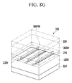
Referring FIG. 8G, the transfer structure 700 is transferred to the display panel 1000 in a state in which heat or pressure is applied. At this time, the partition wall 360PW of the transfer structure 700 is disposed to be disposed at the portion corresponding to the vertical light blocking member 220 b that corresponds to the light blocking region of the display panel 1000.
Referring to FIG. 8H, the carrier substrate 320 is separated from the transfer structure 700.
Referring to FIG. 8I, the mother roof layer 360M is hardened to improve the durability of the roof layer 360 that will be formed later. Herein, the hardening temperature is in a range of 150 to 250° C.
Referring to FIG. 8J, a portion of the mother roof layer 360M is removed by using a photomask to expose a portion of the common electrode 270. At this time, the portion of the mother roof layer 360M is removed thereby forming the roof layer 360.
Referring to FIG. 8K, the exposed portion of the common electrode 270 is etched to be removed. Here, a plurality of microcavities 305 and liquid crystal injection hole formation regions 307FP partitioned by the partition wall 360PW may be formed on the display panel 1000. Then, the liquid crystal material is dripped into the liquid crystal injection hole formation region 307FP, and then injected into the microcavities 305 through the liquid crystal injection hole 307 provided at an inlet of the microcavities 305. An aligning material may be injected into the microcavities 305 before the injection of the liquid crystal material.
Referring to FIG. 8L, a capping layer 390 is formed to fill the liquid crystal injection hole formation region 307FP. Although not shown, a polarizer may be attached to a lower side of the insulating substrate 110 and an upper side of the capping layer 390.
The transfer structures 400 and 700 are formed by a nano-imprinting method, however it is not limited thereto, and the transfer structures 400 and 700 according to the present exemplary embodiment may be formed through various methods such as a roll printing method.
While the inventive concept has been described in connection with what is presently considered to be practical exemplary embodiments, it is to be understood that the inventive concept is not limited to the disclosed embodiments, but, on the contrary, is intended to cover various modifications and equivalent arrangements included within the spirit and scope of the appended claims.
<Description of Symbols>
310 liquid crystal molecules 305 microcavity
307 liquid crystal injection hole 360 roof layer
360PW partition wall 390 capping layer

Claims (8)

What is claimed is:
1. A liquid crystal display comprising:
a substrate;
a thin film transistor disposed on the substrate;
a pixel electrode disposed on the thin film transistor; and
a roof layer facing the pixel electrode,
wherein a plurality of microcavities are disposed between the pixel electrode and the roof layer, the microcavities include a liquid crystal material,
a partition wall between the microcavities, wherein the partition wall is substantially perpendicular to the roof layer, the partition wall is protruded at the roof layer, and the partition wall and the roof layer are integrally formed.
2. The liquid crystal display of claim 1, further comprising
a capping layer disposed on the roof layer, and the capping layer contacts an upper surface of the roof layer.
3. The liquid crystal display of claim 2, wherein
a liquid crystal injection hole formation region is disposed between the microcavities, and the capping layer covers the liquid crystal injection hole formation region.
4. The liquid crystal display of claim 3, wherein
a side surface of the roof layer contacting the capping layer in the liquid crystal injection hole formation region is substantially perpendicular to the substrate.
5. The liquid crystal display of claim 4, further comprising
a common electrode facing the pixel electrode via a passivation layer interposed therebetween.
6. A liquid crystal display comprising:
a substrate;
a thin film transistor disposed on the substrate;
a pixel electrode disposed on the thin film transistor; and
a roof layer facing the pixel electrode,
wherein a plurality of microcavities are disposed between the pixel electrode and the roof layer, the microcavities include a liquid crystal material,
a partition wall between the microcavities, wherein the partition wall is substantially perpendicular to the roof layer;
a common electrode disposed between the microcavities and the roof layer, wherein
the common electrode is disposed between the partition wall and the roof layer.
7. The liquid crystal display of claim 6, wherein
the common electrode has a surface parallel to the substrate at the partition wall.
8. The liquid crystal display of claim 7, wherein
the common electrode and the roof layer are in contact.
US14/308,104 2014-01-15 2014-06-18 Liquid crystal display and method of manufacturing the same Expired - Fee Related US9551895B2 (en)

Applications Claiming Priority (2)

Application Number Priority Date Filing Date Title
KR10-2014-0005308 2014-01-15
KR1020140005308A KR20150085437A (en) 2014-01-15 2014-01-15 Liquid crystal display and method of manufacturing the same

Publications (2)

Publication Number Publication Date
US20150198840A1 US20150198840A1 (en) 2015-07-16
US9551895B2 true US9551895B2 (en) 2017-01-24

Family

ID=53521258

Family Applications (1)

Application Number Title Priority Date Filing Date
US14/308,104 Expired - Fee Related US9551895B2 (en) 2014-01-15 2014-06-18 Liquid crystal display and method of manufacturing the same

Country Status (2)

Country Link
US (1) US9551895B2 (en)
KR (1) KR20150085437A (en)

Families Citing this family (2)

* Cited by examiner, † Cited by third party
Publication number Priority date Publication date Assignee Title
JP2016070949A (en) * 2014-09-26 2016-05-09 株式会社ジャパンディスプレイ Display device
KR102471019B1 (en) * 2015-09-02 2022-11-25 삼성디스플레이 주식회사 Etchant composition and method of fabricating thin film transistor substrate using the same

Citations (12)

* Cited by examiner, † Cited by third party
Publication number Priority date Publication date Assignee Title
US5949508A (en) * 1997-12-10 1999-09-07 Kent State University Phase separated composite organic film and methods for the manufacture thereof
US5956112A (en) * 1995-10-02 1999-09-21 Sharp Kabushiki Kaisha Liquid crystal display device and method for manufacturing the same
US6141072A (en) 1997-04-04 2000-10-31 Georgia Tech Research Corporation System and method for efficient manufacturing of liquid crystal displays
KR20080070190A (en) 2007-01-25 2008-07-30 삼성전자주식회사 Spacer formation apparatus for liquid crystal display
KR100890211B1 (en) 2007-11-09 2009-03-25 고려대학교 산학협력단 Non-volatile memory device manufacturing method using the nano-imprinting techniques
US7612859B2 (en) * 2005-10-31 2009-11-03 Hewlett-Packard Development Company, L.P. Ultra-violet radiation absorbing grid
US20120062448A1 (en) * 2010-09-10 2012-03-15 Kim Yeun Tae Display apparatus and manufacturing method thereof
KR101145867B1 (en) 2009-11-20 2012-05-15 고려대학교 산학협력단 Method of forming nanostructures on a substrate by direct transfer of nanostructure with Spin-on glass
KR20120067751A (en) 2010-12-16 2012-06-26 삼성전자주식회사 Method of forming nano imprint lithography pattern
JP2013074258A (en) 2011-09-29 2013-04-22 Fujifilm Corp Nanoimprint method and nanoimprint device for use therein and manufacturing method of patterned substrate
US20130242228A1 (en) * 2012-03-15 2013-09-19 Samsung Display Co., Ltd. Liquid crystal display and manufacturing method thereof
US20130250220A1 (en) * 2012-03-23 2013-09-26 Samsung Display Co., Ltd. Liquid crystal display and manufacturing method thereof

Patent Citations (12)

* Cited by examiner, † Cited by third party
Publication number Priority date Publication date Assignee Title
US5956112A (en) * 1995-10-02 1999-09-21 Sharp Kabushiki Kaisha Liquid crystal display device and method for manufacturing the same
US6141072A (en) 1997-04-04 2000-10-31 Georgia Tech Research Corporation System and method for efficient manufacturing of liquid crystal displays
US5949508A (en) * 1997-12-10 1999-09-07 Kent State University Phase separated composite organic film and methods for the manufacture thereof
US7612859B2 (en) * 2005-10-31 2009-11-03 Hewlett-Packard Development Company, L.P. Ultra-violet radiation absorbing grid
KR20080070190A (en) 2007-01-25 2008-07-30 삼성전자주식회사 Spacer formation apparatus for liquid crystal display
KR100890211B1 (en) 2007-11-09 2009-03-25 고려대학교 산학협력단 Non-volatile memory device manufacturing method using the nano-imprinting techniques
KR101145867B1 (en) 2009-11-20 2012-05-15 고려대학교 산학협력단 Method of forming nanostructures on a substrate by direct transfer of nanostructure with Spin-on glass
US20120062448A1 (en) * 2010-09-10 2012-03-15 Kim Yeun Tae Display apparatus and manufacturing method thereof
KR20120067751A (en) 2010-12-16 2012-06-26 삼성전자주식회사 Method of forming nano imprint lithography pattern
JP2013074258A (en) 2011-09-29 2013-04-22 Fujifilm Corp Nanoimprint method and nanoimprint device for use therein and manufacturing method of patterned substrate
US20130242228A1 (en) * 2012-03-15 2013-09-19 Samsung Display Co., Ltd. Liquid crystal display and manufacturing method thereof
US20130250220A1 (en) * 2012-03-23 2013-09-26 Samsung Display Co., Ltd. Liquid crystal display and manufacturing method thereof

Also Published As

Publication number Publication date
KR20150085437A (en) 2015-07-23
US20150198840A1 (en) 2015-07-16

Similar Documents

Publication Publication Date Title
US8614781B2 (en) Liquid crystal display and manufacturing method thereof having particular capping layer
US8908126B2 (en) Liquid crystal display and manufacturing method thereof
US8896801B2 (en) Liquid crystal display and manufacturing method thereof
US20140055726A1 (en) Liquid crystal display and manufacturing method thereof
US9201265B2 (en) Liquid crystal display and method of manufacturing the same
US20160124275A1 (en) Liquid crystal display having improved transmittance
US9348164B2 (en) Liquid crystal display and method of manufacturing the same
US20170075164A1 (en) Liquid crystal display and manufacturing method thereof
US9772516B2 (en) Liquid crystal display and method of manufacturing the same
US9551895B2 (en) Liquid crystal display and method of manufacturing the same
US9372370B2 (en) Liquid crystal display and method of manufacturing the same
KR102098304B1 (en) Liquid crystal display and manufacturing method thereor
US9785002B2 (en) Liquid crystal display and method of manufacturing the same
EP3002626B1 (en) Liquid crystal display and method of manufacturing the same
US9897842B2 (en) Display device and manufacturing method thereof
US9671633B2 (en) Display device and method of manufacturing the same
US9645429B2 (en) Display device and manufacturing method thereof
US9638947B2 (en) Display device including a groove patterned loof layer and manufacturing method thereof
US20160291411A1 (en) Liquid crystal display and manufacturing method thereof
US9575349B2 (en) Liquid crystal display and method of manufacturing the same
US20150234227A1 (en) Liquid crystal display and method of manufacturing the same
US20170184914A1 (en) Liquid crystal display and manufacturing method thereof
KR20150121387A (en) Display device and manufacturing method thereof

Legal Events

Date Code Title Description
AS Assignment

Owner name: SAMSUNG DISPLAY CO., LTD., KOREA, REPUBLIC OF

Free format text: ASSIGNMENT OF ASSIGNORS INTEREST;ASSIGNORS:JUNG, YANG-HO;HONG, PIL SOON;PARK, JUN HONG;AND OTHERS;REEL/FRAME:033130/0465

Effective date: 20140523

FEPP Fee payment procedure

Free format text: PAYOR NUMBER ASSIGNED (ORIGINAL EVENT CODE: ASPN); ENTITY STATUS OF PATENT OWNER: LARGE ENTITY

STCF Information on status: patent grant

Free format text: PATENTED CASE

FEPP Fee payment procedure

Free format text: MAINTENANCE FEE REMINDER MAILED (ORIGINAL EVENT CODE: REM.); ENTITY STATUS OF PATENT OWNER: LARGE ENTITY

LAPS Lapse for failure to pay maintenance fees

Free format text: PATENT EXPIRED FOR FAILURE TO PAY MAINTENANCE FEES (ORIGINAL EVENT CODE: EXP.); ENTITY STATUS OF PATENT OWNER: LARGE ENTITY

STCH Information on status: patent discontinuation

Free format text: PATENT EXPIRED DUE TO NONPAYMENT OF MAINTENANCE FEES UNDER 37 CFR 1.362

FP Lapsed due to failure to pay maintenance fee

Effective date: 20210124