US9548213B2 - Dielectric isolated fin with improved fin profile - Google Patents
Dielectric isolated fin with improved fin profile Download PDFInfo
- Publication number
- US9548213B2 US9548213B2 US14/189,294 US201414189294A US9548213B2 US 9548213 B2 US9548213 B2 US 9548213B2 US 201414189294 A US201414189294 A US 201414189294A US 9548213 B2 US9548213 B2 US 9548213B2
- Authority
- US
- United States
- Prior art keywords
- fin structures
- dielectric
- semiconductor
- spacers
- forming
- Prior art date
- Legal status (The legal status is an assumption and is not a legal conclusion. Google has not performed a legal analysis and makes no representation as to the accuracy of the status listed.)
- Active, expires
Links
- 239000004065 semiconductor Substances 0.000 claims abstract description 157
- 125000006850 spacer group Chemical group 0.000 claims abstract description 152
- 238000000034 method Methods 0.000 claims abstract description 93
- 239000000758 substrate Substances 0.000 claims abstract description 48
- 230000001590 oxidative effect Effects 0.000 claims abstract description 14
- 239000000463 material Substances 0.000 claims description 81
- NJPPVKZQTLUDBO-UHFFFAOYSA-N novaluron Chemical compound C1=C(Cl)C(OC(F)(F)C(OC(F)(F)F)F)=CC=C1NC(=O)NC(=O)C1=C(F)C=CC=C1F NJPPVKZQTLUDBO-UHFFFAOYSA-N 0.000 claims description 24
- 238000005530 etching Methods 0.000 claims description 23
- 230000003647 oxidation Effects 0.000 claims description 16
- 238000007254 oxidation reaction Methods 0.000 claims description 16
- 238000000137 annealing Methods 0.000 claims description 14
- 238000000151 deposition Methods 0.000 claims description 7
- 229910021420 polycrystalline silicon Inorganic materials 0.000 claims description 4
- 229910021417 amorphous silicon Inorganic materials 0.000 claims description 3
- 230000007935 neutral effect Effects 0.000 claims description 3
- 239000010410 layer Substances 0.000 description 67
- 239000003989 dielectric material Substances 0.000 description 17
- VYPSYNLAJGMNEJ-UHFFFAOYSA-N Silicium dioxide Chemical compound O=[Si]=O VYPSYNLAJGMNEJ-UHFFFAOYSA-N 0.000 description 15
- XUIMIQQOPSSXEZ-UHFFFAOYSA-N Silicon Chemical compound [Si] XUIMIQQOPSSXEZ-UHFFFAOYSA-N 0.000 description 15
- 229920002120 photoresistant polymer Polymers 0.000 description 15
- 229910052710 silicon Inorganic materials 0.000 description 15
- 239000010703 silicon Substances 0.000 description 15
- 229910052814 silicon oxide Inorganic materials 0.000 description 15
- 238000001020 plasma etching Methods 0.000 description 12
- 238000005229 chemical vapour deposition Methods 0.000 description 10
- 239000004020 conductor Substances 0.000 description 7
- 150000004767 nitrides Chemical class 0.000 description 7
- 230000005669 field effect Effects 0.000 description 6
- 238000000623 plasma-assisted chemical vapour deposition Methods 0.000 description 6
- 229910000577 Silicon-germanium Inorganic materials 0.000 description 5
- 238000005137 deposition process Methods 0.000 description 5
- 238000000231 atomic layer deposition Methods 0.000 description 4
- 230000008021 deposition Effects 0.000 description 4
- 238000010884 ion-beam technique Methods 0.000 description 4
- 238000000608 laser ablation Methods 0.000 description 4
- 229910052581 Si3N4 Inorganic materials 0.000 description 3
- PNEYBMLMFCGWSK-UHFFFAOYSA-N aluminium oxide Inorganic materials [O-2].[O-2].[O-2].[Al+3].[Al+3] PNEYBMLMFCGWSK-UHFFFAOYSA-N 0.000 description 3
- 230000015572 biosynthetic process Effects 0.000 description 3
- 239000000969 carrier Substances 0.000 description 3
- 229910000449 hafnium oxide Inorganic materials 0.000 description 3
- 229910052751 metal Inorganic materials 0.000 description 3
- 239000002184 metal Substances 0.000 description 3
- 238000000206 photolithography Methods 0.000 description 3
- 229910010271 silicon carbide Inorganic materials 0.000 description 3
- -1 siloxanes Chemical class 0.000 description 3
- OKTJSMMVPCPJKN-UHFFFAOYSA-N Carbon Chemical compound [C] OKTJSMMVPCPJKN-UHFFFAOYSA-N 0.000 description 2
- GWEVSGVZZGPLCZ-UHFFFAOYSA-N Titan oxide Chemical compound O=[Ti]=O GWEVSGVZZGPLCZ-UHFFFAOYSA-N 0.000 description 2
- MCMNRKCIXSYSNV-UHFFFAOYSA-N Zirconium dioxide Chemical compound O=[Zr]=O MCMNRKCIXSYSNV-UHFFFAOYSA-N 0.000 description 2
- LEVVHYCKPQWKOP-UHFFFAOYSA-N [Si].[Ge] Chemical compound [Si].[Ge] LEVVHYCKPQWKOP-UHFFFAOYSA-N 0.000 description 2
- 229910052782 aluminium Inorganic materials 0.000 description 2
- 238000001505 atmospheric-pressure chemical vapour deposition Methods 0.000 description 2
- QVGXLLKOCUKJST-UHFFFAOYSA-N atomic oxygen Chemical compound [O] QVGXLLKOCUKJST-UHFFFAOYSA-N 0.000 description 2
- 229910052799 carbon Inorganic materials 0.000 description 2
- 238000000224 chemical solution deposition Methods 0.000 description 2
- 239000002019 doping agent Substances 0.000 description 2
- 239000011521 glass Substances 0.000 description 2
- 229910052735 hafnium Inorganic materials 0.000 description 2
- VBJZVLUMGGDVMO-UHFFFAOYSA-N hafnium atom Chemical compound [Hf] VBJZVLUMGGDVMO-UHFFFAOYSA-N 0.000 description 2
- WIHZLLGSGQNAGK-UHFFFAOYSA-N hafnium(4+);oxygen(2-) Chemical compound [O-2].[O-2].[Hf+4] WIHZLLGSGQNAGK-UHFFFAOYSA-N 0.000 description 2
- CJNBYAVZURUTKZ-UHFFFAOYSA-N hafnium(iv) oxide Chemical compound O=[Hf]=O CJNBYAVZURUTKZ-UHFFFAOYSA-N 0.000 description 2
- 229910052739 hydrogen Inorganic materials 0.000 description 2
- 239000001257 hydrogen Substances 0.000 description 2
- 239000012212 insulator Substances 0.000 description 2
- 238000004518 low pressure chemical vapour deposition Methods 0.000 description 2
- 238000004519 manufacturing process Methods 0.000 description 2
- 150000002739 metals Chemical class 0.000 description 2
- 239000000203 mixture Substances 0.000 description 2
- 229910052760 oxygen Inorganic materials 0.000 description 2
- 239000001301 oxygen Substances 0.000 description 2
- 230000000737 periodic effect Effects 0.000 description 2
- 238000005268 plasma chemical vapour deposition Methods 0.000 description 2
- 229920005591 polysilicon Polymers 0.000 description 2
- 150000003376 silicon Chemical class 0.000 description 2
- HQVNEWCFYHHQES-UHFFFAOYSA-N silicon nitride Chemical compound N12[Si]34N5[Si]62N3[Si]51N64 HQVNEWCFYHHQES-UHFFFAOYSA-N 0.000 description 2
- 229910021483 silicon-carbon alloy Inorganic materials 0.000 description 2
- 239000000126 substance Substances 0.000 description 2
- JBRZTFJDHDCESZ-UHFFFAOYSA-N AsGa Chemical compound [As]#[Ga] JBRZTFJDHDCESZ-UHFFFAOYSA-N 0.000 description 1
- ZOXJGFHDIHLPTG-UHFFFAOYSA-N Boron Chemical group [B] ZOXJGFHDIHLPTG-UHFFFAOYSA-N 0.000 description 1
- GYHNNYVSQQEPJS-UHFFFAOYSA-N Gallium Chemical compound [Ga] GYHNNYVSQQEPJS-UHFFFAOYSA-N 0.000 description 1
- 229910000927 Ge alloy Inorganic materials 0.000 description 1
- UFHFLCQGNIYNRP-UHFFFAOYSA-N Hydrogen Chemical compound [H][H] UFHFLCQGNIYNRP-UHFFFAOYSA-N 0.000 description 1
- GPXJNWSHGFTCBW-UHFFFAOYSA-N Indium phosphide Chemical compound [In]#P GPXJNWSHGFTCBW-UHFFFAOYSA-N 0.000 description 1
- 229910002244 LaAlO3 Inorganic materials 0.000 description 1
- OAICVXFJPJFONN-UHFFFAOYSA-N Phosphorus Chemical group [P] OAICVXFJPJFONN-UHFFFAOYSA-N 0.000 description 1
- 229910000676 Si alloy Inorganic materials 0.000 description 1
- 229910007991 Si-N Inorganic materials 0.000 description 1
- 229910003811 SiGeC Inorganic materials 0.000 description 1
- 229910006294 Si—N Inorganic materials 0.000 description 1
- 229910002370 SrTiO3 Inorganic materials 0.000 description 1
- 150000004645 aluminates Chemical class 0.000 description 1
- XAGFODPZIPBFFR-UHFFFAOYSA-N aluminium Chemical compound [Al] XAGFODPZIPBFFR-UHFFFAOYSA-N 0.000 description 1
- 229910052787 antimony Inorganic materials 0.000 description 1
- WATWJIUSRGPENY-UHFFFAOYSA-N antimony atom Chemical compound [Sb] WATWJIUSRGPENY-UHFFFAOYSA-N 0.000 description 1
- 229910052785 arsenic Inorganic materials 0.000 description 1
- RQNWIZPPADIBDY-UHFFFAOYSA-N arsenic atom Chemical compound [As] RQNWIZPPADIBDY-UHFFFAOYSA-N 0.000 description 1
- 229910052796 boron Inorganic materials 0.000 description 1
- YZYDPPZYDIRSJT-UHFFFAOYSA-K boron phosphate Chemical compound [B+3].[O-]P([O-])([O-])=O YZYDPPZYDIRSJT-UHFFFAOYSA-K 0.000 description 1
- 229910000149 boron phosphate Inorganic materials 0.000 description 1
- 239000012159 carrier gas Substances 0.000 description 1
- 239000011248 coating agent Substances 0.000 description 1
- 238000000576 coating method Methods 0.000 description 1
- 230000001447 compensatory effect Effects 0.000 description 1
- 150000001875 compounds Chemical class 0.000 description 1
- 229910052802 copper Inorganic materials 0.000 description 1
- 229910052593 corundum Inorganic materials 0.000 description 1
- 239000013078 crystal Substances 0.000 description 1
- 239000002178 crystalline material Substances 0.000 description 1
- 230000008020 evaporation Effects 0.000 description 1
- 238000001704 evaporation Methods 0.000 description 1
- 229910052733 gallium Inorganic materials 0.000 description 1
- 239000007789 gas Substances 0.000 description 1
- 229910052732 germanium Inorganic materials 0.000 description 1
- GNPVGFCGXDBREM-UHFFFAOYSA-N germanium atom Chemical compound [Ge] GNPVGFCGXDBREM-UHFFFAOYSA-N 0.000 description 1
- 229910021478 group 5 element Inorganic materials 0.000 description 1
- 150000002431 hydrogen Chemical class 0.000 description 1
- 229910052738 indium Inorganic materials 0.000 description 1
- RPQDHPTXJYYUPQ-UHFFFAOYSA-N indium arsenide Chemical compound [In]#[As] RPQDHPTXJYYUPQ-UHFFFAOYSA-N 0.000 description 1
- APFVFJFRJDLVQX-UHFFFAOYSA-N indium atom Chemical compound [In] APFVFJFRJDLVQX-UHFFFAOYSA-N 0.000 description 1
- 150000002500 ions Chemical class 0.000 description 1
- MRELNEQAGSRDBK-UHFFFAOYSA-N lanthanum oxide Inorganic materials [O-2].[O-2].[O-2].[La+3].[La+3] MRELNEQAGSRDBK-UHFFFAOYSA-N 0.000 description 1
- 239000007788 liquid Substances 0.000 description 1
- 229910052914 metal silicate Inorganic materials 0.000 description 1
- 229910003465 moissanite Inorganic materials 0.000 description 1
- KTUFCUMIWABKDW-UHFFFAOYSA-N oxo(oxolanthaniooxy)lanthanum Chemical compound O=[La]O[La]=O KTUFCUMIWABKDW-UHFFFAOYSA-N 0.000 description 1
- 238000000059 patterning Methods 0.000 description 1
- 229910052698 phosphorus Inorganic materials 0.000 description 1
- 239000011574 phosphorus Substances 0.000 description 1
- 238000002360 preparation method Methods 0.000 description 1
- 230000005855 radiation Effects 0.000 description 1
- 230000000717 retained effect Effects 0.000 description 1
- 239000005368 silicate glass Substances 0.000 description 1
- 150000004760 silicates Chemical class 0.000 description 1
- 229910021332 silicide Inorganic materials 0.000 description 1
- FVBUAEGBCNSCDD-UHFFFAOYSA-N silicide(4-) Chemical compound [Si-4] FVBUAEGBCNSCDD-UHFFFAOYSA-N 0.000 description 1
- 239000002356 single layer Substances 0.000 description 1
- 229910052719 titanium Inorganic materials 0.000 description 1
- 229910052721 tungsten Inorganic materials 0.000 description 1
- 229910001845 yogo sapphire Inorganic materials 0.000 description 1
- RUDFQVOCFDJEEF-UHFFFAOYSA-N yttrium(III) oxide Inorganic materials [O-2].[O-2].[O-2].[Y+3].[Y+3] RUDFQVOCFDJEEF-UHFFFAOYSA-N 0.000 description 1
Images


Classifications
-
- H—ELECTRICITY
- H01—ELECTRIC ELEMENTS
- H01L—SEMICONDUCTOR DEVICES NOT COVERED BY CLASS H10
- H01L29/00—Semiconductor devices adapted for rectifying, amplifying, oscillating or switching, or capacitors or resistors with at least one potential-jump barrier or surface barrier, e.g. PN junction depletion layer or carrier concentration layer; Details of semiconductor bodies or of electrodes thereof ; Multistep manufacturing processes therefor
- H01L29/66—Types of semiconductor device ; Multistep manufacturing processes therefor
- H01L29/68—Types of semiconductor device ; Multistep manufacturing processes therefor controllable by only the electric current supplied, or only the electric potential applied, to an electrode which does not carry the current to be rectified, amplified or switched
- H01L29/76—Unipolar devices, e.g. field effect transistors
- H01L29/772—Field effect transistors
- H01L29/78—Field effect transistors with field effect produced by an insulated gate
- H01L29/7842—Field effect transistors with field effect produced by an insulated gate means for exerting mechanical stress on the crystal lattice of the channel region, e.g. using a flexible substrate
- H01L29/7846—Field effect transistors with field effect produced by an insulated gate means for exerting mechanical stress on the crystal lattice of the channel region, e.g. using a flexible substrate the means being located in the lateral device isolation region, e.g. STI
-
- H—ELECTRICITY
- H01—ELECTRIC ELEMENTS
- H01L—SEMICONDUCTOR DEVICES NOT COVERED BY CLASS H10
- H01L21/00—Processes or apparatus adapted for the manufacture or treatment of semiconductor or solid state devices or of parts thereof
- H01L21/02—Manufacture or treatment of semiconductor devices or of parts thereof
- H01L21/02104—Forming layers
- H01L21/02107—Forming insulating materials on a substrate
- H01L21/02225—Forming insulating materials on a substrate characterised by the process for the formation of the insulating layer
- H01L21/02227—Forming insulating materials on a substrate characterised by the process for the formation of the insulating layer formation by a process other than a deposition process
- H01L21/0223—Forming insulating materials on a substrate characterised by the process for the formation of the insulating layer formation by a process other than a deposition process formation by oxidation, e.g. oxidation of the substrate
- H01L21/02233—Forming insulating materials on a substrate characterised by the process for the formation of the insulating layer formation by a process other than a deposition process formation by oxidation, e.g. oxidation of the substrate of the semiconductor substrate or a semiconductor layer
- H01L21/02236—Forming insulating materials on a substrate characterised by the process for the formation of the insulating layer formation by a process other than a deposition process formation by oxidation, e.g. oxidation of the substrate of the semiconductor substrate or a semiconductor layer group IV semiconductor
-
- H—ELECTRICITY
- H01—ELECTRIC ELEMENTS
- H01L—SEMICONDUCTOR DEVICES NOT COVERED BY CLASS H10
- H01L21/00—Processes or apparatus adapted for the manufacture or treatment of semiconductor or solid state devices or of parts thereof
- H01L21/02—Manufacture or treatment of semiconductor devices or of parts thereof
- H01L21/04—Manufacture or treatment of semiconductor devices or of parts thereof the devices having at least one potential-jump barrier or surface barrier, e.g. PN junction, depletion layer or carrier concentration layer
- H01L21/18—Manufacture or treatment of semiconductor devices or of parts thereof the devices having at least one potential-jump barrier or surface barrier, e.g. PN junction, depletion layer or carrier concentration layer the devices having semiconductor bodies comprising elements of Group IV of the Periodic System or AIIIBV compounds with or without impurities, e.g. doping materials
- H01L21/30—Treatment of semiconductor bodies using processes or apparatus not provided for in groups H01L21/20 - H01L21/26
- H01L21/302—Treatment of semiconductor bodies using processes or apparatus not provided for in groups H01L21/20 - H01L21/26 to change their surface-physical characteristics or shape, e.g. etching, polishing, cutting
- H01L21/306—Chemical or electrical treatment, e.g. electrolytic etching
- H01L21/30604—Chemical etching
-
- H—ELECTRICITY
- H01—ELECTRIC ELEMENTS
- H01L—SEMICONDUCTOR DEVICES NOT COVERED BY CLASS H10
- H01L21/00—Processes or apparatus adapted for the manufacture or treatment of semiconductor or solid state devices or of parts thereof
- H01L21/02—Manufacture or treatment of semiconductor devices or of parts thereof
- H01L21/04—Manufacture or treatment of semiconductor devices or of parts thereof the devices having at least one potential-jump barrier or surface barrier, e.g. PN junction, depletion layer or carrier concentration layer
- H01L21/18—Manufacture or treatment of semiconductor devices or of parts thereof the devices having at least one potential-jump barrier or surface barrier, e.g. PN junction, depletion layer or carrier concentration layer the devices having semiconductor bodies comprising elements of Group IV of the Periodic System or AIIIBV compounds with or without impurities, e.g. doping materials
- H01L21/30—Treatment of semiconductor bodies using processes or apparatus not provided for in groups H01L21/20 - H01L21/26
- H01L21/302—Treatment of semiconductor bodies using processes or apparatus not provided for in groups H01L21/20 - H01L21/26 to change their surface-physical characteristics or shape, e.g. etching, polishing, cutting
- H01L21/306—Chemical or electrical treatment, e.g. electrolytic etching
- H01L21/308—Chemical or electrical treatment, e.g. electrolytic etching using masks
- H01L21/3083—Chemical or electrical treatment, e.g. electrolytic etching using masks characterised by their size, orientation, disposition, behaviour, shape, in horizontal or vertical plane
- H01L21/3086—Chemical or electrical treatment, e.g. electrolytic etching using masks characterised by their size, orientation, disposition, behaviour, shape, in horizontal or vertical plane characterised by the process involved to create the mask, e.g. lift-off masks, sidewalls, or to modify the mask, e.g. pre-treatment, post-treatment
-
- H—ELECTRICITY
- H01—ELECTRIC ELEMENTS
- H01L—SEMICONDUCTOR DEVICES NOT COVERED BY CLASS H10
- H01L21/00—Processes or apparatus adapted for the manufacture or treatment of semiconductor or solid state devices or of parts thereof
- H01L21/02—Manufacture or treatment of semiconductor devices or of parts thereof
- H01L21/04—Manufacture or treatment of semiconductor devices or of parts thereof the devices having at least one potential-jump barrier or surface barrier, e.g. PN junction, depletion layer or carrier concentration layer
- H01L21/18—Manufacture or treatment of semiconductor devices or of parts thereof the devices having at least one potential-jump barrier or surface barrier, e.g. PN junction, depletion layer or carrier concentration layer the devices having semiconductor bodies comprising elements of Group IV of the Periodic System or AIIIBV compounds with or without impurities, e.g. doping materials
- H01L21/30—Treatment of semiconductor bodies using processes or apparatus not provided for in groups H01L21/20 - H01L21/26
- H01L21/31—Treatment of semiconductor bodies using processes or apparatus not provided for in groups H01L21/20 - H01L21/26 to form insulating layers thereon, e.g. for masking or by using photolithographic techniques; After treatment of these layers; Selection of materials for these layers
- H01L21/3105—After-treatment
- H01L21/31051—Planarisation of the insulating layers
-
- H—ELECTRICITY
- H01—ELECTRIC ELEMENTS
- H01L—SEMICONDUCTOR DEVICES NOT COVERED BY CLASS H10
- H01L21/00—Processes or apparatus adapted for the manufacture or treatment of semiconductor or solid state devices or of parts thereof
- H01L21/02—Manufacture or treatment of semiconductor devices or of parts thereof
- H01L21/04—Manufacture or treatment of semiconductor devices or of parts thereof the devices having at least one potential-jump barrier or surface barrier, e.g. PN junction, depletion layer or carrier concentration layer
- H01L21/18—Manufacture or treatment of semiconductor devices or of parts thereof the devices having at least one potential-jump barrier or surface barrier, e.g. PN junction, depletion layer or carrier concentration layer the devices having semiconductor bodies comprising elements of Group IV of the Periodic System or AIIIBV compounds with or without impurities, e.g. doping materials
- H01L21/30—Treatment of semiconductor bodies using processes or apparatus not provided for in groups H01L21/20 - H01L21/26
- H01L21/31—Treatment of semiconductor bodies using processes or apparatus not provided for in groups H01L21/20 - H01L21/26 to form insulating layers thereon, e.g. for masking or by using photolithographic techniques; After treatment of these layers; Selection of materials for these layers
- H01L21/3105—After-treatment
- H01L21/311—Etching the insulating layers by chemical or physical means
- H01L21/31105—Etching inorganic layers
- H01L21/31111—Etching inorganic layers by chemical means
-
- H—ELECTRICITY
- H01—ELECTRIC ELEMENTS
- H01L—SEMICONDUCTOR DEVICES NOT COVERED BY CLASS H10
- H01L21/00—Processes or apparatus adapted for the manufacture or treatment of semiconductor or solid state devices or of parts thereof
- H01L21/02—Manufacture or treatment of semiconductor devices or of parts thereof
- H01L21/04—Manufacture or treatment of semiconductor devices or of parts thereof the devices having at least one potential-jump barrier or surface barrier, e.g. PN junction, depletion layer or carrier concentration layer
- H01L21/18—Manufacture or treatment of semiconductor devices or of parts thereof the devices having at least one potential-jump barrier or surface barrier, e.g. PN junction, depletion layer or carrier concentration layer the devices having semiconductor bodies comprising elements of Group IV of the Periodic System or AIIIBV compounds with or without impurities, e.g. doping materials
- H01L21/30—Treatment of semiconductor bodies using processes or apparatus not provided for in groups H01L21/20 - H01L21/26
- H01L21/324—Thermal treatment for modifying the properties of semiconductor bodies, e.g. annealing, sintering
-
- H—ELECTRICITY
- H01—ELECTRIC ELEMENTS
- H01L—SEMICONDUCTOR DEVICES NOT COVERED BY CLASS H10
- H01L21/00—Processes or apparatus adapted for the manufacture or treatment of semiconductor or solid state devices or of parts thereof
- H01L21/70—Manufacture or treatment of devices consisting of a plurality of solid state components formed in or on a common substrate or of parts thereof; Manufacture of integrated circuit devices or of parts thereof
- H01L21/71—Manufacture of specific parts of devices defined in group H01L21/70
- H01L21/76—Making of isolation regions between components
- H01L21/762—Dielectric regions, e.g. EPIC dielectric isolation, LOCOS; Trench refilling techniques, SOI technology, use of channel stoppers
- H01L21/76224—Dielectric regions, e.g. EPIC dielectric isolation, LOCOS; Trench refilling techniques, SOI technology, use of channel stoppers using trench refilling with dielectric materials
-
- H—ELECTRICITY
- H01—ELECTRIC ELEMENTS
- H01L—SEMICONDUCTOR DEVICES NOT COVERED BY CLASS H10
- H01L29/00—Semiconductor devices adapted for rectifying, amplifying, oscillating or switching, or capacitors or resistors with at least one potential-jump barrier or surface barrier, e.g. PN junction depletion layer or carrier concentration layer; Details of semiconductor bodies or of electrodes thereof ; Multistep manufacturing processes therefor
- H01L29/02—Semiconductor bodies ; Multistep manufacturing processes therefor
- H01L29/06—Semiconductor bodies ; Multistep manufacturing processes therefor characterised by their shape; characterised by the shapes, relative sizes, or dispositions of the semiconductor regions ; characterised by the concentration or distribution of impurities within semiconductor regions
- H01L29/0603—Semiconductor bodies ; Multistep manufacturing processes therefor characterised by their shape; characterised by the shapes, relative sizes, or dispositions of the semiconductor regions ; characterised by the concentration or distribution of impurities within semiconductor regions characterised by particular constructional design considerations, e.g. for preventing surface leakage, for controlling electric field concentration or for internal isolations regions
- H01L29/0642—Isolation within the component, i.e. internal isolation
- H01L29/0649—Dielectric regions, e.g. SiO2 regions, air gaps
- H01L29/0653—Dielectric regions, e.g. SiO2 regions, air gaps adjoining the input or output region of a field-effect device, e.g. the source or drain region
-
- H—ELECTRICITY
- H01—ELECTRIC ELEMENTS
- H01L—SEMICONDUCTOR DEVICES NOT COVERED BY CLASS H10
- H01L29/00—Semiconductor devices adapted for rectifying, amplifying, oscillating or switching, or capacitors or resistors with at least one potential-jump barrier or surface barrier, e.g. PN junction depletion layer or carrier concentration layer; Details of semiconductor bodies or of electrodes thereof ; Multistep manufacturing processes therefor
- H01L29/02—Semiconductor bodies ; Multistep manufacturing processes therefor
- H01L29/06—Semiconductor bodies ; Multistep manufacturing processes therefor characterised by their shape; characterised by the shapes, relative sizes, or dispositions of the semiconductor regions ; characterised by the concentration or distribution of impurities within semiconductor regions
- H01L29/10—Semiconductor bodies ; Multistep manufacturing processes therefor characterised by their shape; characterised by the shapes, relative sizes, or dispositions of the semiconductor regions ; characterised by the concentration or distribution of impurities within semiconductor regions with semiconductor regions connected to an electrode not carrying current to be rectified, amplified or switched and such electrode being part of a semiconductor device which comprises three or more electrodes
- H01L29/1025—Channel region of field-effect devices
- H01L29/1029—Channel region of field-effect devices of field-effect transistors
- H01L29/1033—Channel region of field-effect devices of field-effect transistors with insulated gate, e.g. characterised by the length, the width, the geometric contour or the doping structure
- H01L29/1054—Channel region of field-effect devices of field-effect transistors with insulated gate, e.g. characterised by the length, the width, the geometric contour or the doping structure with a variation of the composition, e.g. channel with strained layer for increasing the mobility
-
- H—ELECTRICITY
- H01—ELECTRIC ELEMENTS
- H01L—SEMICONDUCTOR DEVICES NOT COVERED BY CLASS H10
- H01L29/00—Semiconductor devices adapted for rectifying, amplifying, oscillating or switching, or capacitors or resistors with at least one potential-jump barrier or surface barrier, e.g. PN junction depletion layer or carrier concentration layer; Details of semiconductor bodies or of electrodes thereof ; Multistep manufacturing processes therefor
- H01L29/66—Types of semiconductor device ; Multistep manufacturing processes therefor
- H01L29/66007—Multistep manufacturing processes
- H01L29/66075—Multistep manufacturing processes of devices having semiconductor bodies comprising group 14 or group 13/15 materials
- H01L29/66227—Multistep manufacturing processes of devices having semiconductor bodies comprising group 14 or group 13/15 materials the devices being controllable only by the electric current supplied or the electric potential applied, to an electrode which does not carry the current to be rectified, amplified or switched, e.g. three-terminal devices
- H01L29/66409—Unipolar field-effect transistors
- H01L29/66477—Unipolar field-effect transistors with an insulated gate, i.e. MISFET
- H01L29/6653—Unipolar field-effect transistors with an insulated gate, i.e. MISFET using the removal of at least part of spacer, e.g. disposable spacer
-
- H—ELECTRICITY
- H01—ELECTRIC ELEMENTS
- H01L—SEMICONDUCTOR DEVICES NOT COVERED BY CLASS H10
- H01L29/00—Semiconductor devices adapted for rectifying, amplifying, oscillating or switching, or capacitors or resistors with at least one potential-jump barrier or surface barrier, e.g. PN junction depletion layer or carrier concentration layer; Details of semiconductor bodies or of electrodes thereof ; Multistep manufacturing processes therefor
- H01L29/66—Types of semiconductor device ; Multistep manufacturing processes therefor
- H01L29/66007—Multistep manufacturing processes
- H01L29/66075—Multistep manufacturing processes of devices having semiconductor bodies comprising group 14 or group 13/15 materials
- H01L29/66227—Multistep manufacturing processes of devices having semiconductor bodies comprising group 14 or group 13/15 materials the devices being controllable only by the electric current supplied or the electric potential applied, to an electrode which does not carry the current to be rectified, amplified or switched, e.g. three-terminal devices
- H01L29/66409—Unipolar field-effect transistors
- H01L29/66477—Unipolar field-effect transistors with an insulated gate, i.e. MISFET
- H01L29/66553—Unipolar field-effect transistors with an insulated gate, i.e. MISFET using inside spacers, permanent or not
-
- H—ELECTRICITY
- H01—ELECTRIC ELEMENTS
- H01L—SEMICONDUCTOR DEVICES NOT COVERED BY CLASS H10
- H01L29/00—Semiconductor devices adapted for rectifying, amplifying, oscillating or switching, or capacitors or resistors with at least one potential-jump barrier or surface barrier, e.g. PN junction depletion layer or carrier concentration layer; Details of semiconductor bodies or of electrodes thereof ; Multistep manufacturing processes therefor
- H01L29/66—Types of semiconductor device ; Multistep manufacturing processes therefor
- H01L29/66007—Multistep manufacturing processes
- H01L29/66075—Multistep manufacturing processes of devices having semiconductor bodies comprising group 14 or group 13/15 materials
- H01L29/66227—Multistep manufacturing processes of devices having semiconductor bodies comprising group 14 or group 13/15 materials the devices being controllable only by the electric current supplied or the electric potential applied, to an electrode which does not carry the current to be rectified, amplified or switched, e.g. three-terminal devices
- H01L29/66409—Unipolar field-effect transistors
- H01L29/66477—Unipolar field-effect transistors with an insulated gate, i.e. MISFET
- H01L29/6656—Unipolar field-effect transistors with an insulated gate, i.e. MISFET using multiple spacer layers, e.g. multiple sidewall spacers
-
- H—ELECTRICITY
- H01—ELECTRIC ELEMENTS
- H01L—SEMICONDUCTOR DEVICES NOT COVERED BY CLASS H10
- H01L29/00—Semiconductor devices adapted for rectifying, amplifying, oscillating or switching, or capacitors or resistors with at least one potential-jump barrier or surface barrier, e.g. PN junction depletion layer or carrier concentration layer; Details of semiconductor bodies or of electrodes thereof ; Multistep manufacturing processes therefor
- H01L29/66—Types of semiconductor device ; Multistep manufacturing processes therefor
- H01L29/66007—Multistep manufacturing processes
- H01L29/66075—Multistep manufacturing processes of devices having semiconductor bodies comprising group 14 or group 13/15 materials
- H01L29/66227—Multistep manufacturing processes of devices having semiconductor bodies comprising group 14 or group 13/15 materials the devices being controllable only by the electric current supplied or the electric potential applied, to an electrode which does not carry the current to be rectified, amplified or switched, e.g. three-terminal devices
- H01L29/66409—Unipolar field-effect transistors
- H01L29/66477—Unipolar field-effect transistors with an insulated gate, i.e. MISFET
- H01L29/66787—Unipolar field-effect transistors with an insulated gate, i.e. MISFET with a gate at the side of the channel
- H01L29/66795—Unipolar field-effect transistors with an insulated gate, i.e. MISFET with a gate at the side of the channel with a horizontal current flow in a vertical sidewall of a semiconductor body, e.g. FinFET, MuGFET
-
- H—ELECTRICITY
- H01—ELECTRIC ELEMENTS
- H01L—SEMICONDUCTOR DEVICES NOT COVERED BY CLASS H10
- H01L29/00—Semiconductor devices adapted for rectifying, amplifying, oscillating or switching, or capacitors or resistors with at least one potential-jump barrier or surface barrier, e.g. PN junction depletion layer or carrier concentration layer; Details of semiconductor bodies or of electrodes thereof ; Multistep manufacturing processes therefor
- H01L29/66—Types of semiconductor device ; Multistep manufacturing processes therefor
- H01L29/68—Types of semiconductor device ; Multistep manufacturing processes therefor controllable by only the electric current supplied, or only the electric potential applied, to an electrode which does not carry the current to be rectified, amplified or switched
- H01L29/76—Unipolar devices, e.g. field effect transistors
- H01L29/772—Field effect transistors
- H01L29/78—Field effect transistors with field effect produced by an insulated gate
- H01L29/785—Field effect transistors with field effect produced by an insulated gate having a channel with a horizontal current flow in a vertical sidewall of a semiconductor body, e.g. FinFET, MuGFET
- H01L29/7851—Field effect transistors with field effect produced by an insulated gate having a channel with a horizontal current flow in a vertical sidewall of a semiconductor body, e.g. FinFET, MuGFET with the body tied to the substrate
Definitions
- the present disclosure relates generally to semiconductor fabrication, and more particularly to structures and methods for forming fin field effect transistors (FinFETs).
- FinFETs fin field effect transistors
- a fin structure is formed by a method that includes forming a plurality of fin structures from a bulk semiconductor substrate, and forming a dielectric spacer on a sidewall of the plurality of fin structure.
- a semiconductor spacer is formed on a sidewall of the dielectric spacer.
- An exposed portion of the bulk substrate that is present between the semiconductor spacers on adjacent fin structures is etched to form a pedestal portion of the bulk substrate.
- a dielectric fill is formed in the space between the adjacent fin structures.
- the semiconductor spacer and a portion of the fin structures that is present below a lower surface of the dielectric spacer are annealed, wherein the annealing of the portions of the fin structures that are below the lower surface of the dielectric spacer produces a first strain and annealing the semiconductor spacer produces a second strain that is opposite the first strain.
- a fin structure is formed by a method that includes forming a plurality of fin structures from a bulk semiconductor substrate.
- a first dielectric fill is formed in the space between the adjacent fin structures.
- the sidewalls of the upper portion of the plurality of fin structures are exposed.
- a dielectric spacer is formed on the exposed sidewalls of at least one fin structure in the plurality of fin structure.
- a semiconductor spacer is formed on a sidewall of the dielectric spacer.
- a second dielectric fill is formed on the space between the adjacent fin structures on the first dielectric fill.
- the semiconductor spacer and a portion of the fin structures that is present below a lower surface of the dielectric spacer is annealed, wherein annealing the portion of the fin structures below the lower surface of the dielectric spacer produces a first strain and annealing the semiconductor spacer produces a second strain that is opposite the first strain.
- a fin field effect transistor having a uniform tail region.
- the finFET includes a fin structure that is present on a dielectric surface.
- the fin structure includes a uniform tail region that is present at an interface of the fin structure and dielectric surface.
- a gate structure is present on a channel portion of the fin structure and includes a gate dielectric in contact with the channel portion of the fin structure and at least one gate conductor.
- a source region and a drain region are present on opposing sides of the channel portion of the fin structure.
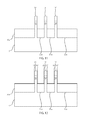
- FIG. 1 is a side cross-sectional view of forming a plurality of fin structures from a bulk semiconductor substrate, in accordance with one embodiment of the present disclosure
- FIG. 2 is a side cross-sectional view depicting forming a dielectric spacer on a sidewall of at least one fin structure in the plurality of fin structures, in accordance with one embodiment of the present disclosure.
- FIG. 3 is a side cross-sectional view depicting one embodiment of forming a conformal layer of a semiconductor material on the dielectric spacer, the plurality of fin structures and upper surface of bulk substrate that is present between adjacent fin structures in the plurality of fin structures, in accordance with the present disclosure.
- FIG. 4 is a side cross-sectional view depicting one embodiment of etching the conformal layer of the semiconductor material to provide semiconductor spacers on a sidewall of the dielectric spacer, and etching an exposed portion of the bulk substrate to provide a pedestal portion of the bulk substrate, in accordance with the present disclosure.
- FIG. 5 is a side cross-sectional view depicting etching the pedestal portion of the fin structures to reduce the width of the pedestal portion to be substantially equal to the width of the upper portion of the fin structures, in accordance with one embodiment of the present disclosure.
- FIG. 6 is a side cross-sectional view depicting forming a dielectric fill in the space between the adjacent fin structures.
- FIG. 7 is a side cross-sectional view depicting oxidizing a portion of the fin structures that is present below a lower surface of the dielectric spacer, in accordance with one embodiment of the present disclosure.
- FIG. 8 is a side cross-sectional view depicting recessing the dielectric fill, in accordance with one embodiment of the present disclosure.
- FIG. 9 is a side cross-sectional view depicting removing the dielectric spacer from the sidewall of the fin structures.
- FIG. 10 is a side cross-sectional view depicting one embodiment of a finFET structure that may be formed using the process flow that is depicted in FIGS. 1-9 , in accordance with the present disclosure.
- FIG. 11 is a side cross-sectional view depicting another embodiment of a method for forming a fin structure, in which a plurality of fin structures are formed from a bulk semiconductor substrate, and a first dielectric fill is formed in the space between the adjacent fin structures.
- FIG. 12 is a side cross-sectional view depicting forming a dielectric spacer on the exposed sidewalls of each fin structure in the plurality of fin structures that are depicted in FIG. 11 , in accordance with one embodiment of the present disclosure.
- FIG. 13 is a side cross-sectional view depicting one embodiment of forming a conformal layer of a semiconductor material on the dielectric spacer, the plurality of fin structures and upper surface of first dielectric fill that is present between adjacent fin structures of the plurality of fin structures that are depicted in FIG. 12 , in accordance with the present disclosure.
- FIG. 14 is a side cross-sectional view depicting one embodiment of anisotropically etching the conformal layer of the semiconductor material to provide semiconductor spacers on a sidewall of the dielectric spacer, in accordance with the present disclosure.
- FIG. 15 is a side cross-sectional view depicting forming a second dielectric fill in the space between the adjacent fin structures on the first dielectric fill, in accordance with one embodiment of the present disclosure.
- FIG. 16 is a side cross-sectional view depicting one embodiment of oxidizing the semiconductor spacer and a portion of the fin structures that is present below a lower surface of the dielectric spacer, in accordance with the present disclosure.
- the terms “upper”, “lower”, “right”, “left”, “vertical”, “horizontal”, “top”, “bottom”, and derivatives thereof shall relate to the embodiments of the disclosure, as it is oriented in the drawing figures.
- the term “positioned on” means that a first element, such as a first structure, is present on a second element, such as a second structure, wherein intervening elements, such as an interface structure, e.g. interface layer, may be present between the first element and the second element.
- intervening elements such as an interface structure, e.g. interface layer
- directly contact means that a first element, such as a first structure, and a second element, such as a second structure, are connected without any intermediary conducting, insulating or semiconductor layers at the interface of the two elements.
- the methods and structures disclosed herein form a region of a dielectric material, e.g., oxide, under a fin structure that is formed from a bulk semiconductor substrate.
- a “fin structure” refers to a semiconductor material, which can be employed as the body of a semiconductor device, in which the gate structure is positioned around the fin structure such that charge flows down the channel on the two sidewalls of the fin structure and optionally along the top surface of the fin structure.
- the methods and structures disclosed herein substantially reduce or eliminate stresses induced in the fin structures from the underlying region of the dielectric material, e.g., oxide, by oxidizing a semiconductor spacer that is adjacent to the fin structures. Oxidizing the semiconductor spacer produces a compensatory stress that neutralizes the stress being formed in the fin structures by the underlying region of dielectric material.
- FIG. 1 depicts one embodiment of forming a plurality of fin structures 10 from a bulk semiconductor substrate 5 .
- a “bulk semiconductor substrate” is a substrate that is composed of a single semiconductor material.
- a bulk semiconductor substrate 5 does not include a buried dielectric layer that is typically present in silicon on insulator (SOI) substrates.
- SOI silicon on insulator
- the semiconductor material that provides the bulk semiconductor substrate 5 may be a semiconducting material including, but not limited to silicon, strained silicon, a silicon carbon alloy (e.g., silicon doped with carbon (Si:C), silicon germainum, a silicon germanium and carbon alloy (e.g., silicon germanium doped with carbon (SiGe:C), silicon alloys, germanium, germanium alloys, gallium arsenic, indium arsenic, indium phosphide, as well as other III/V and II/VI compound semiconductors.
- silicon silicon carbon alloy
- Si:C silicon doped with carbon
- SiGe:C silicon germanium doped with carbon
- silicon alloys germanium, germanium alloys, gallium arsenic, indium arsenic, indium phosphide, as well as other III/V and II/VI compound semiconductors.
- the plurality of fin structures 10 may be formed from the bulk semiconductor substrate 5 , using photolithography and etch processes. For example, prior to etching the bulk semiconductor substrate 5 to provide the plurality of fin structures 10 , a layer of the dielectric material is deposited atop the upper surface of the bulk semiconductor substrate 5 to provide a dielectric fin cap 15 .
- the material layer that provides the dielectric fin cap 15 may be composed of a nitride, oxide, oxynitride material, and/or any other suitable dielectric layer.
- the dielectric fin cap 15 may comprise a single layer of dielectric material or multiple layers of dielectric materials.
- the material layer that provides the dielectric fin cap 15 can be formed by a deposition process, such as chemical vapor deposition (CVD) and/or atomic layer deposition (ALD). Alternatively, the material layer that provides the dielectric fin cap 15 may be formed using a growth process, such as thermal oxidation or thermal nitridation. The material layer that provides the dielectric fin cap 15 may have a thickness ranging from 1 nm to 100 nm. In one example, the dielectric fin cap 15 is composed of an oxide, such as SiO 2 , that is formed by CVD to a thickness ranging from 25 nm to 50 nm.
- a photolithography and etch process sequence is applied to the material layer for the dielectric fin cap 15 and the bulk semiconductor substrate 5 .
- a photoresist mask is formed overlying the layer of the dielectric material that provides dielectric fin cap 15 and is present overlying the bulk semiconductor substrate 5 , in which the portion of the dielectric material that is underlying the photoresist mask provides the dielectric fin cap 15 , and the portion of the bulk semiconductor substrate 5 that is underlying the photoresist mask provides the plurality of fin structures 10 .
- a photoresist layer is first positioned on the layer of the dielectric material that provides dielectric fin cap 15 .
- the photoresist layer may be provided by a blanket layer of photoresist material that is formed utilizing a deposition process such as, e.g., plasma enhanced CVD (PECVD), evaporation or spin-on coating.
- PECVD plasma enhanced CVD
- the blanket layer of photoresist material is then patterned to provide the photoresist mask utilizing a lithographic process that may include exposing the photoresist material to a pattern of radiation and developing the exposed photoresist material utilizing a resist developer.
- an etching process may remove the unprotected portions of the dielectric material that provides the dielectric fin cap 15 followed by removing a portion of the exposed bulk semiconductor substrate 5 selectively to the photoresist mask.
- the transferring of the pattern provided by the photoresist into the underlying structures may include an anisotropic etch.
- an “anisotropic etch process” denotes a material removal process in which the etch rate in the direction normal to the surface to be etched is greater than in the direction parallel to the surface to be etched.
- the anisotropic etch may include reactive-ion etching (RIE).
- RIE reactive-ion etching
- Other examples of anisotropic etching that can be used at this point of the present disclosure include ion beam etching, plasma etching or laser ablation.
- the etch process may be timed to determine the height of the fin structures 10 .
- Each of the fin structures 10 may have a height H 1 ranging from 5 nm to 200 nm. In another embodiment, each of the fin structures 10 has a height H 1 ranging from 10 nm to 100 nm. In one example, each of the fin structures 10 has a height H 1 ranging from 20 nm to 50 nm. Each of the plurality of fin structures 10 may have a width W 1 of less than 20 nm. In another embodiment, each of the fin structures 10 has a width W 1 ranging from 3 nm to 8 nm. Although three fin structures 10 are depicted in FIG. 1 , the present disclosure is not limited to only this example. It is noted that any number of fin structures 10 may be formed from the bulk semiconductor substrate 5 . The pitch P 1 separating adjacent fin structures in the plurality of fin structures 10 may range from 15 nm to 200 nm. In another example, the pitch P 1 separating adjacent fin structures 10 may range from 15 nm to 100 nm.
- FIG. 2 depicts one embodiment of forming a dielectric spacer 20 on a sidewall of each fin structure 10 .
- the dielectric spacer 20 typically extends across an entirety of a height of the sidewall for each of the plurality of fin structures 10 , and in some embodiments may extend onto the sidewall of the dielectric fin cap 15 .
- the dielectric spacer 20 is typically composed of a dielectric material, such as an oxides (with the exception of silicon oxide), nitrides or oxynitrides (with the exception of silicon oxynitride).
- the dielectric spacer 20 may be composed of hafnium oxide (HfO 2 ), silicon carbides (SiCN), silicon carbonitrides, silsequioxanes, siloxanes, boron phosphate silicate glass (BPSG) and combinations thereof.
- the dielectric spacer 20 may be formed by a process sequence that includes depositing a conformal dielectric layer on the plurality of the fin structures 15 and an exposed upper surface of the bulk semiconductor substrate 5 that is present between adjacent fin structures 10 .
- the term “conformal” denotes a layer having a thickness that does not deviate from greater than or less than 30% of an average value for the thickness of the layer.
- the conformal dielectric layer for forming the dielectric spacer 20 may be formed using a CVD process, such as PECVD, or the conformal dielectric layer may be deposited using a spin on deposition process.
- an anisotropic etch process may remove the horizontal portions of the conformal dielectric layer, wherein the vertical portions of the conformal dielectric layer remain to provide the dielectric spacer 20 .
- the horizontal portions of the conformal dielectric layer are the portions of the dialectic layer that are present on the upper surface of the dielectric fin cap 15 and the surfaces of the portion of the bulk semiconductor substrate 5 that are present between adjacent fin structures 10 .
- the anisotropic etch process for removing the horizontal portions of the conformal dielectric layer may be a RIE process.
- the width of the dielectric spacer 20 may range from 3 nm to 15 nm.
- FIG. 3 depicts one embodiment of forming a conformal layer of a semiconductor material 25 on the dielectric spacer 20 , the dielectric fin cap 15 , the plurality of fin structures 10 and upper surface of bulk semiconductor substrate 5 that is present between adjacent fin structures 10 .
- the conformal layer of semiconductor material 25 may be composed of an amorphous semiconductor material or a multi-crystalline, e.g., polycrystalline, semiconductor material.
- An amorphous semiconductor material is a non-crystalline material that lacks the long-range order characteristic of a crystal.
- a polycrystalline structure is a form of semiconductor material made up of randomly oriented crystallites and containing large-angle grain boundaries, twin boundaries or both. Multi-crystalline is widely referred to a polycrystalline material with large grains (of the order of millimeters to centimeters).
- the term polycrystalline typically refers to small grains (hundreds of nanometers, to hundreds of microns).
- the conformal layer of the semiconductor material 25 may be composed of a silicon containing material.
- silicon-containing materials suitable for the semiconductor material include, but are not limited to, Si, SiGe, SiGeC, SiC, polysilicon, i.e., polySi, amorphous Si, i.e., ⁇ :Si, and multi-layers thereof.
- the silicon-containing materials may also include hydrogen, such as hydrogenated silicon (Si:H) or amorpohous hydrogenated silicon ( ⁇ -Si:H). It is noted that the above materials are provided for illustrative purposes only, and are not intended to limit the present disclosure, as other materials are suitable for provided the conformal layer of the semiconductor material 25 .
- any semiconductor material that provides a strain following oxidation may be suitable for use as the material of the conformal layer of the semiconductor material 25 with the methods and structures of the present disclosure.
- the conformal layer of the semiconductor material 25 may have a thickness T 1 ranging from 3 nm to 30 nm. In another embodiment, the conformal layer of the semiconductor material 25 may have a thickness T 1 ranging from 3 nm to 10 nm.
- the conformal layer of the semiconductor material 25 may be deposited using a CVD process, such as Atmospheric Pressure CVD (APCVD), Low Pressure CVD (LPCVD), Plasma Enhanced CVD (EPCVD), Metal-Organic CVD (MOCVD), atomic layer deposition (ALD) and combinations thereof may also be employed.
- APCVD Atmospheric Pressure CVD
- LPCVD Low Pressure CVD
- EPCVD Plasma Enhanced CVD
- MOCVD Metal-Organic CVD
- ALD atomic layer deposition
- FIG. 4 depicts one embodiment of etching the conformal layer of the semiconductor material to provide semiconductor spacers 25 a on a sidewall of the dielectric spacer 20 , and etching an exposed portion of the bulk semiconductor substrate 5 to provide a pedestal portion 30 of the bulk semiconductor substrate 5 .
- the etch process for forming the semiconductor spacers 25 a and the pedestal portion 30 of the bulk semiconductor substrate 5 may be a anisotropic etch, such as RIE, ion beam etching, plasma etching or laser ablation.
- the etch process for forming the semiconductor spacers 25 a and the pedestal portion 30 of the bulk semiconductor substrate 5 may be an etch that removes the material of the semiconductor spacers 25 a and the bulk semiconductor substrate 5 selectively to the material of the dielectric fin cap 15 .
- the term “selective” in reference to a material removal process denotes that the rate of material removal for a first material is greater than the rate of removal for at least another material of the structure to which the material removal process is being applied.
- a selective etch may include an etch chemistry that removes a first material selectively to a second material by a ratio of 100:1 or greater, e.g., 1000:1.
- the etch process for forming semiconductor spacers 25 a and the pedestal portion 30 of the bulk semiconductor substrate 5 is continued until the horizontal portions of the conformal layer of the semiconductor material are removed in their entirety, and the remaining vertical portions of the conformal layer of the semiconductor material that are present on the sidewalls of the dielectric spacer 20 are recessed so that the height of the semiconductor spacers 25 a is less than half the height H 1 of the fin structures 10 .
- the portion of the bulk semiconductor substrate 5 that is present between the semiconductor spacers 25 a is etched to provide a trench 35 having a height H 2 ranging from 10 nm to 200 nm.
- the depth H 2 of the trench 35 defines the height of the pedestal portion 30 of the fin structures 10 .
- the height H 4 of the semiconductor spacers 25 a ranges from 10 nm to 100 nm. In another embodiment, the height H 4 of the semiconductor spacers 25 a ranges from 20 nm to 50 nm. In one embodiment, the width W 4 of the semiconductor spacers 25 a ranges from 3 nm to 30 nm. In yet another embodiment, the width W 4 of the semiconductor spacers 25 a ranges from 3 nm to 10 nm.
- FIG. 5 depicts one embodiment of etching the pedestal portion 30 of the fin structures 10 to reduce the width W 2 of the pedestal portion 30 to be substantially equal to the width W 1 of the fin structures 10 .
- “By substantially equal” it is meant that the width W 2 of the pedestal portion 30 may be within +/ ⁇ 5 nm of the width W 1 of the fin structures 10 .
- the pedestal portion 30 may be etched using an isotropic etch.
- the term “isotropic etch” denotes an etch process that is non-directional. By “non-directional” it is meant that the etch rate is not substantially greater in any one direction in comparison to all of the etch directions.
- the isotropic etch may be a wet chemical etch or a dry etch.
- the etchant may be a corrosive liquid or a chemically active ionized gas, such as a plasma.
- the etch process for reducing the width W 2 of the pedestal portion 30 of the fin structures 10 may be selective to the semiconductor spacers 25 a , the dielectric spacers 20 , and the dielectric fin cap 15 .
- the step of etching the pedestal portion 30 of the fin structures 10 may be omitted.
- FIG. 6 depicts one embodiment of forming a dielectric fill 35 in the space between the adjacent fin structures 10 including the trenches between the pedestal portions 30 of the fin structures 10 .
- FIG. 6 depicts forming the dielectric fill 35 between the adjacent fin structures 10 that are depicted in FIG. 4
- the step of forming the dielectric fill 35 is equally applicable to the embodiments of the present disclosure that include the step of reducing the width of the pedestal portion 30 of the fin structures 10 as described above with reference to FIG. 5 .
- the dielectric fill 35 may be an oxide containing material.
- the dielectric fill 35 may be silicon oxide (SiO 2 ).
- Other examples of materials that may be employed for the dielectric fill 35 include silicon nitride, silicon oxynitride, hafnium oxide, hafnium oxynitride, alumina and combinations thereof.
- the dielectric fill 35 may be formed using CVD, PECVD, high-density plasma CVD (HPCVD), chemical solution deposition or a spin-on glass process. Following deposition, the material for the dielectric fill 35 may be planarized so that the upper surface of the dielectric fill is coplanar with the upper surface of the dielectric fin cap 15 .
- FIG. 7 depicts oxidizing a portion (hereafter referred to as oxidized base portion 40 ) of the fin structures 10 that is present below a lower surface of the dielectric spacer 20 .
- the semiconductor spacer is also oxidized (hereafter referred to as oxidized semiconductor spacer 25 b ).
- the oxidized base portion 40 produces a first strain and the oxidized semiconductor spacer 25 b produces a second strain that is opposite the first strain.
- oxidizing the portion of the fin structures 10 to provide the oxidizing base portion 40 produces an intrinsic strain within the oxidized base portion 40 .
- intrinsic strain refers to a stress or presence of a strain, either compressive or tensile, which is developed during preparation of a structure and can therefore be retained in the structure without external force.
- the mechanical strain can be imparted to the fin structure 10 , due to volume expansion of the oxide as compared with silicon.
- the intrinsic strain that is present in the oxidized base portion 40 induces a strain on the overlying fin structures 10 . Therefore, the direction of the strain is in a direction, i.e., first direction D 1 , that extends from the base of the fin structure 10 towards an upper surface of the fin structure 10 .
- the intrinsic strain that is present in the oxidized base portion 40 of the fin structures 10 may range from 0.3 GPa tensile to ⁇ 0.3 GPa compressive strain.
- the oxidized base portion 40 may have a width W 3 ranging from 15 nm to 50 nm, and a height H 3 ranging from 10 nm to 200 nm.
- the oxidized base portion 40 may have a width W 3 ranging from 15 nm to 35 nm, and a height H 3 ranging from 35 nm to 70 nm.
- the semiconductor spacer is also oxidized to form the oxidized semiconductor spacer 25 b , which has a second strain in a direction D 2 opposite to the direction D 1 of first strain produced by the oxidized base portion 40 .
- the strain produced in the oxidized semiconductor spacer 25 b may be an intrinsic strain. More specifically, the intrinsic strain that is present in the oxidized semiconductor spacer 25 b may range from 0.3 GPa tensile to ⁇ 0.3 GPa compressive stress.
- the oxidized semiconductor spacer 25 b is formed on a sidewall of the fin structure 10 and induces a strain in an opposite direction, i.e., second direction D 2 , as the strain being induced by the oxidized base portion 40 .
- the direction of the strain, i.e., second direction D 2 , induced by the oxidized semiconductor spacer 25 b may extend in a direction from the oxidized semiconductor spacer 25 b towards the oxidized base portion 40 .
- the substantially relaxed fin structure 10 may also be referred to as having a substantially neutral strain state.
- a fin structure that is substantially relaxed is a fin structure 10 having a strain no greater than about +/ ⁇ 0.1 GPa tensile or compressive.
- the strain that can be measured in the fin structure 10 that results from the opposing strains produced by the oxidized semiconductor spacer 25 b and the oxidized base portion 40 may range from 0.1 GPa tensile to ⁇ 0.1 GPa compressive strain.
- the strain that can be measured in the fin structure 10 that results from the opposing strains produced by the oxidized semiconductor spacer 25 b and the oxidized base portion 40 may range from 0.05 GPa tensile to ⁇ 0.05 GPa compressive strain. In one example, the fin structure 10 may be completely relaxed.
- the oxidation process that produces the oxidized semiconductor spacer 25 b and the oxidized base portion 40 may be a thermal oxidation process.
- the thermal oxidation process includes annealing in an oxygen containing atmosphere, which may include a hydrogen carrier gas.
- the oxidation occurs in a furnace set to a temperature in the range of 900° C. to 1300° C. In another embodiment, the oxidation occurs in a furnace set to a temperature in the range of 950° C. to 1200° C.
- oxygen from the furnace atmosphere diffuses through the dielectric fill 35 to react with the semiconductor material, e.g., silicon, of the bulk semiconductor substrate 5 and the semiconductor spacers 25 a , forming oxide, which includes the oxidized semiconductor spacer 25 b and the oxidized base portion 40 formed at the base of the fin structure 10 , leaving an unoxidized portion of the fin structure 10 present between the dielectric fin cap 15 and the oxidized base portion 40 .
- the oxide of the oxidized semiconductor spacer 25 b and the oxidized base portion 40 may be silicon oxide (SiO 2 ).
- an oxide region 50 having a triangular-shaped cross-section or tail profile (hereafter referred to as a tail region 50 ) is present at an interface between the unoxidized portion of the fin structure 10 and the oxidized base portion 40 of the fin structure 10 .
- the tail region 50 may be uniform.
- a “uniform” tail region 50 is a tail region having a height H 5 of 5 nm or less. Due to the aforementioned stress balancing between oxidized semiconductor spacer 25 and pedestal 30 , the amount of mechanical stress is reduced, and tail height H 5 is reduced because of the less stress-enhanced oxidation
- the dielectric fill 35 being in direct physical contact with the fin structures 10 , the fin structure 10 is held firmly in place by the dielectric fill 35 during the formation of the oxidized base portion 40 , and so the undesirable mechanical shift is prevented.
- FIG. 8 depicts one embodiment of recessing the dielectric fill 35 .
- the dielectric fill 35 may be recessed using an anisotropic etch process, that removes the material of the dielectric fill 35 selectively to the dielectric fin cap 15 .
- the etch process for recessing the dielectric fill 35 may also be selective to the dielectric spacers 20 .
- One example of an etch process for recessing the dielectric fill includes RIE.
- anisotropic etching that can be used at this point of the present disclosure include ion beam etching, plasma etching or laser ablation.
- the anisotropic etch is timed so that the dielectric fill 35 is recessed to expose the dielectric spacers 20 .
- the etch process that recessed the dielectric fill 35 will also remove the oxidized semiconductor spacer 25 b .
- the methods and structures disclosed herein address the stress non-uniformity that occurs during oxidation, that causes unbalanced oxidation rates and therefore, non-uniform fin tail.
- the fin tail is reduced with a balanced stress profile along the height.
- FIG. 9 depicts one embodiment of removing the dielectric spacer 20 from the sidewall of the fin structures 10 .
- the dielectric spacer 20 may be removed using an etch process that removes the material of the dielectric spacer 20 selectively to the fin structures 10 , the remaining portion of the dielectric fill 35 and the tail region 50 .
- the etch process for removing the dielectric spacer 20 may be an anisotropic etch, such as RIE.
- the etch process for removing the dielectric spacer 20 may be an isotropic etch, such as a wet chemical etch or a dry etch, e.g., plasma etch.
- the etch process for removing the dielectric spacer 20 may also remove the dielectric fin cap 15 .
- Removing the dielectric fin cap 15 is optional.
- the dielectric fin cap 15 may remain when the fin structure 10 is employed in a fin field effect transistor (finFET), and the dielectric fin cap 15 is removed the fin structure 10 is employed in a tri-gate semiconductor device.
- finFET fin field effect transistor
- FIG. 10 is a of a finFET structure 100 that may be formed using the fin structure 10 formed by the process flow that is depicted in FIGS. 1-9 .
- a “field effect transistor (FET)” is a semiconductor device in which the output current, i.e., source-drain current, is controlled by the voltage applied to the gate.
- a FET has three terminals, i.e., gate structure, source region and drain region.
- a gate structure is a structure used to control output current (i.e., flow of carriers in the channel) of a semiconducting device through electrical or magnetic fields.
- a finFET is a field effect transistor in which at least the channel portion of the field effect transistor is present in a fin structure 10 .
- the channel is the region underlying the gate structure and between the source and drain of a semiconductor device that becomes conductive when the semiconductor device is turned on.
- FIG. 10 only depicts two finFET devices being formed from two fin structures 10 , any number of finFET devices may be formed using any number of fin structures 10 .
- each of the finFET devices includes a gate structure 110 that may be composed of at least one gate dielectric layer 111 , at least one gate conductor layer 112 and at least one gate dielectric cap 113 .
- the at least one gate dielectric layer 111 is composed of an insulator, and is present between the channel region of the fin structure 10 and the at least one gate conductor layer 112 of the gate structure 110 .
- the gate structure 110 may be formed by forming blanket material layers for the at least one gate dielectric layer 111 , the at least one gate conductor layer 112 , and the at least one gate dielectric cap 112 to provide a gate stack, and patterning and etching the gate stack to provide the gate structure 110 utilizing photolithography and etch process steps.
- the at least one gate dielectric layer 111 is typically positioned on at least a portion of the sidewalls of the fin structures 10 .
- the at least one gate dielectric layer 111 may be formed by a thermal growth process such as, e.g., oxidation, nitridation or oxynitridation. In other embodiments, the at least one gate dielectric layer 111 may be formed using a deposition process, such as CVD.
- the at least one gate dielectric layer 111 is composed of a low-k dielectric material, such as silicon oxide (SiO 2 ), which typically has a dielectric constant of less than 4.0 at room temperature, e.g. 25° C.
- the at least one gate dielectric 111 is composed of a high-k dielectric material.
- High-k dielectric materials have a dielectric constant greater than silicon oxide (SiO 2 ) at room temperature, e.g., 25° C.
- SiO 2 silicon oxide
- a high-k dielectric composed of hafnium oxide (HFO 2 ) may have a dielectric constant of 4.0 or greater.
- the at least one gate dielectric layer 111 may include, but is not limited to, an oxide, nitride, oxynitride and/or silicates including metal silicates, aluminates, titanates and nitrides.
- the oxide may be selected from the group including, but not limited to, SiO 2 , HfO 2 , ZrO 2 , Al 2 O 3 , TiO 2 , La 2 O 3 , SrTiO 3 , LaAlO 3 , Y2O 3 and mixture thereof.
- the physical thickness of the at least one gate dielectric layer 111 may vary, but typically, the at least one gate dielectric layer Ill has a thickness ranging from 1 nm to 10 nm.
- the at least one gate conductor layer 112 may be composed of polysilicon, SiGe, a silicide, a metal or a metal-silicon-nitride, such as Ta—Si—N.
- metals that can be used as the at least one gate conductor layer 112 include, but are not limited to Al, W, Cu, Ti or other like conductive metals.
- the physical thickness of the at least one gate conductor layer 112 may range from 1 nm to 10 nm.
- the gate dielectric cap 113 may be composed of a nitride, oxide, oxynitride material, and/or any other suitable dielectric layer.
- a gate sidewall spacer 114 may be formed in direct contact with the gate structure 110 .
- the gate sidewall spacer 114 may be formed using deposition and etch processes.
- the gate sidewall spacer 114 may be composed of a dielectric material, such as oxides, nitrides or oxynitrides.
- a source region 50 and a drain region may be formed on opposing sides of the gate structure 110 , i.e., on opposing sides of the portion of the fin structure 10 including the channel region.
- the source region 50 is a doped region in the finFET device, in which majority carriers are flowing into the channel region
- the drain region is a doped region in the finFET device located at the end of the channel region, in which carriers are flowing out of the finFET through the drain.
- N-type finFET devices are produced by doping the source region 50 and the drain region with elements from group V of the Periodic Table of Elements.
- the group V element is phosphorus, antimony or arsenic.
- P-type finFET devices are produced by doping the source region 50 and the drain region with elements from group III of the Periodic Table of Elements.
- the group III element is boron, aluminum, gallium or indium.
- the source region 50 and the drain region are formed by ion implanting the exposed portions of the fin structures 10 that are on opposing sides of the gate structure 110 .
- the source region 50 may be formed by epitaxially forming a p-type or n-type dopant on the exposed portion of the fin structure 10 and driving the dopant from the epitaxially formed material into an extension region of the fin structure 10 using an annealing process.
- FIGS. 11-16 depict another method for forming a fin structure 10 ′, in which a plurality of fin structures 10 ′ are formed from a bulk semiconductor substrate 5 ′.
- FIG. 10 depicts one embodiment of forming a plurality of fin structure 10 ′ from a bulk semiconductor substrate 5 ′, and forming a first dielectric fill 35 a in the space, e.g., trenches, between the adjacent fin structures 10 ′.
- the fin structures 10 ′ that are depicted in FIG. 11 are similar to the fin structures 10 that are described above with reference to FIG. 1 . Therefore, the description of the fin structures 10 , the bulk substrate 5 , and the dielectric cap 15 that are depicted in FIG. 1 are suitable for the fin structures 10 ′, the bulk substrate 5 ′, and the dielectric cap 15 ′ that are depicted in FIG. 11 .
- the first dielectric fill 35 a is deposited in the space between the adjacent fin structures 10 ′ using a deposition process, such as CVD, and may be recessed by etch process, such as RIE.
- the first dielectric fill 35 a may be an oxide, nitride or oxynitride material.
- the first dielectric fill 35 a is composed of silicon oxide (SiO 2 ). It is noted that the above provided compositions for the first dielectric fill 35 a are provided for illustrative purposes only, and that the present disclosure is not intended to be limited thereto. For example, the materials described above for the dielectric fill 35 depicted in FIG. 5 are suitable for the first dielectric fill 35 a that is depicted in FIG. 11 .
- the etch process for recessing the first dielectric fill 35 a may be a selective etch process that removes the material of the dielectric fill 35 a selectively to the dielectric cap 15 ′.
- the first dielectric fill 35 a may be recessed until the sidewall for the desired height of the fin structure 10 ′ is exposed.
- FIG. 12 depicts one embodiment of forming a dielectric spacer 20 ′ on the exposed sidewalls of each fin structure 10 ′ that is depicted in FIG. 11 .
- the description of the dielectric spacer 20 that is depicted in FIG. 2 is suitable for one embodiment of the dielectric spacer 20 ′ that is depicted in FIG. 12 .
- FIG. 13 depicts one embodiment of forming a conformal layer of a semiconductor material 25 ′ on the dielectric spacer 20 ′, the plurality of fin structures 10 ′ and upper surface of first dielectric fill 35 a that is present between the adjacent fin structures 10 ′ that are depicted in FIG. 12 .
- the description of the conformal layer of a semiconductor material 25 that is depicted in FIG. 3 is suitable for one embodiment of the conformal layer of a semiconductor material 25 ′ that is depicted in FIG. 13 .
- FIG. 14 depicts one embodiment of etching the conformal layer of the semiconductor material to provide semiconductor spacers 25 a ′ on a sidewall of the dielectric spacer 20 ′.
- the etch process for forming the semiconductor spacers 25 a may be an anisotropic etch, such as RIE, ion beam etching, plasma etching or laser ablation.
- the etch process for forming the semiconductor spacers 25 a ′ may be an etch that removes the material of the semiconductor spacers 25 a ′ selectively to the material of the dielectric cap 15 ′ and the first dielectric fill 35 a′.
- FIG. 15 depicts one embodiment of forming a second dielectric fill 35 b in the space between the adjacent fin structures 10 ′ on the first dielectric fill 35 a .
- the second dielectric fill 35 b may be an oxide containing material.
- the second dielectric fill 35 b may be silicon oxide (SiO 2 ).
- Other examples of materials that may be employed for the second dielectric fill 35 b include silicon nitride, silicon oxynitride, hafnium oxide, hafnium oxynitride, alumina and combinations thereof.
- the dielectric fill may be formed using CVD, PECVD, high-density plasma CVD (HPCVD), chemical solution deposition or a spin-on glass process. Following deposition, the material for the second dielectric fill 35 b may be planarized so that the upper surface of the dielectric fill is coplanar with the upper surface of the dielectric cap 15 .
- FIG. 16 depicts one embodiment of oxidizing the semiconductor spacer to form an oxidized semiconductor spacers 25 b ′, and oxidizing a portion of the fin structures 10 ′ that is present below a lower surface of the dielectric spacer 20 ′ to form an oxidized base portion 40 ′.
- One embodiment for the oxidation step that provides the oxidized semiconductor spacers 25 b ′ and the oxidized base portion 40 ′ is described above with reference to FIG. 7 . Similar to the oxidized base portion 40 and the oxidized semiconductor spacer 25 b that are described above and depicted in FIG. 7 , the oxidized base portion 40 ′ that is depicted in FIG.
- the description of the oxidized semiconductor spacer 25 b , and the second strain produced by the oxidized semiconductor spacer 25 b , that are depicted in FIG. 7 is suitable for the oxidized semiconductor spacer 25 b ′ that is depicted in FIG. 16 .
- the description of the oxidized base portion 40 , and the first strain produced by the oxidized base portion 40 , that is depicted in FIG. 7 is suitable for the oxidized base portion 40 ′ that is depicted in FIG. 16 .
- the strain that can be measured in the relaxed fin structure 10 ′ that results from the opposing strains produced by the oxidized semiconductor spacer 25 b ′ and the oxidized base portion 40 ′ may range from 0.1 GPa tensile to ⁇ 0.1 GPa compressive strain.
- the strain that can be measured in the relaxed fin structure 10 ′ that results from the opposing strains produced by the oxidized semiconductor spacer 25 b ′ and the oxidized base portion 40 ′ may range from 0.05 GPa tensile to ⁇ 0.05 GPa compressive strain.
- the fin structure 10 ′ may be completely relaxed.
- an oxide region 50 ′ having a triangular-shaped cross-section or tail profile (hereafter referred to as a tail region 50 ) is present at an interface between the unoxidized portion of the fin structure 10 ′ and the oxidized base portion 40 ′ of the fin structure 10 ′.
- the tail region 50 may have a height H 5 ′ of less than 5 nm.
- the second dielectric fill 35 b is recessed to expose the dielectric spacers 20 ′, and the dielectric spacers 20 ′ are removed.
- the process sequence for recessing the second dielectric fill 35 b has been described above for recessing the dielectric fill 35 that is depicted in FIG. 7 .
- the process sequence for removing the dielectric spacers 20 ′ has been described above for removing the dielectric spacers 20 that are depicted in FIG. 8 .
- a semiconductor device such as the finFET structure 100 depicted in FIG. 10 may be formed from the fin structures 10 ′ that are formed using the process sequence described with reference to FIGS. 11-16 . Further details regarding forming the gate structure and the source and drain regions for a finFET structure including the fin structure 10 ′ formed using the process sequence depicted in FIGS. 11-16 is described above with reference to FIG. 10 .
- the process sequence for forming the finFET structure 100 depicted in FIG. 10 including the fin structures 10 formed using the method described with reference to FIGS. 1-9 or the fin structures 10 ′ formed using the method described with reference to FIGS. 11-16 includes a gate last process sequence, which is not depicted in the supplied figures.
- a gate last process includes forming a replacement gate structure on the channel portion of the fin structures, forming a spacer on the sidewall of the replacement gate structure, forming source and drain regions on opposing sides of the replacement gate structure, removing the replacement gate structure, and forming a functional gate structure in the space once occupied by the replacement gate structure.
- the replacement gate structure can include sacrificial material that defines the geometry of a later formed functional gate structure that functions to switch the semiconductor device from an “on” to “off” state, and vice versa.
- a process sequence employing a replacement gate structure may be referred to as a “gate last” process sequence. Both gate first and gate last process sequences are applicable to the present disclosure.
Abstract
A method of forming a fin structure that includes forming a plurality of fin structures from a bulk semiconductor substrate and forming a dielectric spacer on a sidewall of each fin structure in the plurality of fin structure. A semiconductor spacer is formed on a sidewall of the dielectric spacer. A dielectric fill is formed in the space between the adjacent fin structures. The semiconductor spacer and a portion of the fin structures that is present below a lower surface of the dielectric spacer are oxidized. Oxidizing a base portion of the fin structures produces a first strain and oxidizing the semiconductor spacer produces a second strain that is opposite the first strain.
Description
Technical Field
The present disclosure relates generally to semiconductor fabrication, and more particularly to structures and methods for forming fin field effect transistors (FinFETs).
Description of the Related Art
With the continuing trend towards miniaturization of integrated circuits (ICs), there is a need for transistors to have higher drive currents with increasingly smaller dimensions. FinFET technology is becoming more prevalent as device size continues to shrink. However, the cost of manufacturing SOI finFETs can be high.
In one embodiment, a fin structure is formed by a method that includes forming a plurality of fin structures from a bulk semiconductor substrate, and forming a dielectric spacer on a sidewall of the plurality of fin structure. A semiconductor spacer is formed on a sidewall of the dielectric spacer. An exposed portion of the bulk substrate that is present between the semiconductor spacers on adjacent fin structures is etched to form a pedestal portion of the bulk substrate. A dielectric fill is formed in the space between the adjacent fin structures. The semiconductor spacer and a portion of the fin structures that is present below a lower surface of the dielectric spacer are annealed, wherein the annealing of the portions of the fin structures that are below the lower surface of the dielectric spacer produces a first strain and annealing the semiconductor spacer produces a second strain that is opposite the first strain.
In another embodiment, a fin structure is formed by a method that includes forming a plurality of fin structures from a bulk semiconductor substrate. A first dielectric fill is formed in the space between the adjacent fin structures. The sidewalls of the upper portion of the plurality of fin structures are exposed. A dielectric spacer is formed on the exposed sidewalls of at least one fin structure in the plurality of fin structure. A semiconductor spacer is formed on a sidewall of the dielectric spacer. A second dielectric fill is formed on the space between the adjacent fin structures on the first dielectric fill. The semiconductor spacer and a portion of the fin structures that is present below a lower surface of the dielectric spacer is annealed, wherein annealing the portion of the fin structures below the lower surface of the dielectric spacer produces a first strain and annealing the semiconductor spacer produces a second strain that is opposite the first strain.
In another aspect of the present disclosure, a fin field effect transistor (finFET) is provided having a uniform tail region. In one embodiment, the finFET includes a fin structure that is present on a dielectric surface. The fin structure includes a uniform tail region that is present at an interface of the fin structure and dielectric surface. A gate structure is present on a channel portion of the fin structure and includes a gate dielectric in contact with the channel portion of the fin structure and at least one gate conductor. A source region and a drain region are present on opposing sides of the channel portion of the fin structure.
The disclosure will provide details in the following description of preferred embodiments with reference to the following figures wherein:
Detailed embodiments of the claimed structures and methods are disclosed herein; however, it is to be understood that the disclosed embodiments are merely illustrative of the claimed structures and methods that may be embodied in various forms. In addition, each of the examples given in connection with the various embodiments are intended to be illustrative, and not restrictive. Further, the figures are not necessarily to scale, some features may be exaggerated to show details of particular components. Therefore, specific structural and functional details disclosed herein are not to be interpreted as limiting, but merely as a representative basis for teaching one skilled in the art to variously employ the methods and structures of the present disclosure. For purposes of the description hereinafter, the terms “upper”, “lower”, “right”, “left”, “vertical”, “horizontal”, “top”, “bottom”, and derivatives thereof shall relate to the embodiments of the disclosure, as it is oriented in the drawing figures. The term “positioned on” means that a first element, such as a first structure, is present on a second element, such as a second structure, wherein intervening elements, such as an interface structure, e.g. interface layer, may be present between the first element and the second element. The term “direct contact” means that a first element, such as a first structure, and a second element, such as a second structure, are connected without any intermediary conducting, insulating or semiconductor layers at the interface of the two elements.
In some embodiments, the methods and structures disclosed herein form a region of a dielectric material, e.g., oxide, under a fin structure that is formed from a bulk semiconductor substrate. As used herein, a “fin structure” refers to a semiconductor material, which can be employed as the body of a semiconductor device, in which the gate structure is positioned around the fin structure such that charge flows down the channel on the two sidewalls of the fin structure and optionally along the top surface of the fin structure. In some embodiments, the methods and structures disclosed herein substantially reduce or eliminate stresses induced in the fin structures from the underlying region of the dielectric material, e.g., oxide, by oxidizing a semiconductor spacer that is adjacent to the fin structures. Oxidizing the semiconductor spacer produces a compensatory stress that neutralizes the stress being formed in the fin structures by the underlying region of dielectric material. The methods and structures of the present disclosure are now discussed with more detail referring to FIGS. 1-16 .
The plurality of fin structures 10 may be formed from the bulk semiconductor substrate 5, using photolithography and etch processes. For example, prior to etching the bulk semiconductor substrate 5 to provide the plurality of fin structures 10, a layer of the dielectric material is deposited atop the upper surface of the bulk semiconductor substrate 5 to provide a dielectric fin cap 15. The material layer that provides the dielectric fin cap 15 may be composed of a nitride, oxide, oxynitride material, and/or any other suitable dielectric layer. The dielectric fin cap 15 may comprise a single layer of dielectric material or multiple layers of dielectric materials. The material layer that provides the dielectric fin cap 15 can be formed by a deposition process, such as chemical vapor deposition (CVD) and/or atomic layer deposition (ALD). Alternatively, the material layer that provides the dielectric fin cap 15 may be formed using a growth process, such as thermal oxidation or thermal nitridation. The material layer that provides the dielectric fin cap 15 may have a thickness ranging from 1 nm to 100 nm. In one example, the dielectric fin cap 15 is composed of an oxide, such as SiO2, that is formed by CVD to a thickness ranging from 25 nm to 50 nm.
In one embodiment, following the formation of the layer of dielectric material that provides the dielectric fin cap 15, a photolithography and etch process sequence is applied to the material layer for the dielectric fin cap 15 and the bulk semiconductor substrate 5. Specifically, in one example, a photoresist mask is formed overlying the layer of the dielectric material that provides dielectric fin cap 15 and is present overlying the bulk semiconductor substrate 5, in which the portion of the dielectric material that is underlying the photoresist mask provides the dielectric fin cap 15, and the portion of the bulk semiconductor substrate 5 that is underlying the photoresist mask provides the plurality of fin structures 10. The exposed portions of the dielectric material that provides dielectric fin cap 15 and the portion of the bulk semiconductor substrate 5, which are not protected by the photoresist mask, are removed using a selective etch process. To provide the photoresist mask, a photoresist layer is first positioned on the layer of the dielectric material that provides dielectric fin cap 15. The photoresist layer may be provided by a blanket layer of photoresist material that is formed utilizing a deposition process such as, e.g., plasma enhanced CVD (PECVD), evaporation or spin-on coating. The blanket layer of photoresist material is then patterned to provide the photoresist mask utilizing a lithographic process that may include exposing the photoresist material to a pattern of radiation and developing the exposed photoresist material utilizing a resist developer.
Following the formation of the photoresist mask, an etching process may remove the unprotected portions of the dielectric material that provides the dielectric fin cap 15 followed by removing a portion of the exposed bulk semiconductor substrate 5 selectively to the photoresist mask. For example, the transferring of the pattern provided by the photoresist into the underlying structures may include an anisotropic etch. As used herein, an “anisotropic etch process” denotes a material removal process in which the etch rate in the direction normal to the surface to be etched is greater than in the direction parallel to the surface to be etched. The anisotropic etch may include reactive-ion etching (RIE). Other examples of anisotropic etching that can be used at this point of the present disclosure include ion beam etching, plasma etching or laser ablation. The etch process may be timed to determine the height of the fin structures 10.
Each of the fin structures 10 may have a height H1 ranging from 5 nm to 200 nm. In another embodiment, each of the fin structures 10 has a height H1 ranging from 10 nm to 100 nm. In one example, each of the fin structures 10 has a height H1 ranging from 20 nm to 50 nm. Each of the plurality of fin structures 10 may have a width W1 of less than 20 nm. In another embodiment, each of the fin structures 10 has a width W1 ranging from 3 nm to 8 nm. Although three fin structures 10 are depicted in FIG. 1 , the present disclosure is not limited to only this example. It is noted that any number of fin structures 10 may be formed from the bulk semiconductor substrate 5. The pitch P1 separating adjacent fin structures in the plurality of fin structures 10 may range from 15 nm to 200 nm. In another example, the pitch P1 separating adjacent fin structures 10 may range from 15 nm to 100 nm.
In one embodiment, the dielectric spacer 20 may be formed by a process sequence that includes depositing a conformal dielectric layer on the plurality of the fin structures 15 and an exposed upper surface of the bulk semiconductor substrate 5 that is present between adjacent fin structures 10. The term “conformal” denotes a layer having a thickness that does not deviate from greater than or less than 30% of an average value for the thickness of the layer. In some embodiments, the conformal dielectric layer for forming the dielectric spacer 20 may be formed using a CVD process, such as PECVD, or the conformal dielectric layer may be deposited using a spin on deposition process. Following deposition of the conformal dielectric layer, an anisotropic etch process may remove the horizontal portions of the conformal dielectric layer, wherein the vertical portions of the conformal dielectric layer remain to provide the dielectric spacer 20. The horizontal portions of the conformal dielectric layer are the portions of the dialectic layer that are present on the upper surface of the dielectric fin cap 15 and the surfaces of the portion of the bulk semiconductor substrate 5 that are present between adjacent fin structures 10. The anisotropic etch process for removing the horizontal portions of the conformal dielectric layer may be a RIE process. The width of the dielectric spacer 20 may range from 3 nm to 15 nm.
In one embodiment, the conformal layer of the semiconductor material 25 may be composed of a silicon containing material. Examples of silicon-containing materials suitable for the semiconductor material include, but are not limited to, Si, SiGe, SiGeC, SiC, polysilicon, i.e., polySi, amorphous Si, i.e., α:Si, and multi-layers thereof. The silicon-containing materials may also include hydrogen, such as hydrogenated silicon (Si:H) or amorpohous hydrogenated silicon (α-Si:H). It is noted that the above materials are provided for illustrative purposes only, and are not intended to limit the present disclosure, as other materials are suitable for provided the conformal layer of the semiconductor material 25. For example, any semiconductor material that provides a strain following oxidation may be suitable for use as the material of the conformal layer of the semiconductor material 25 with the methods and structures of the present disclosure. The conformal layer of the semiconductor material 25 may have a thickness T1 ranging from 3 nm to 30 nm. In another embodiment, the conformal layer of the semiconductor material 25 may have a thickness T1 ranging from 3 nm to 10 nm. The conformal layer of the semiconductor material 25 may be deposited using a CVD process, such as Atmospheric Pressure CVD (APCVD), Low Pressure CVD (LPCVD), Plasma Enhanced CVD (EPCVD), Metal-Organic CVD (MOCVD), atomic layer deposition (ALD) and combinations thereof may also be employed.
In some embodiments, the etch process for forming semiconductor spacers 25 a and the pedestal portion 30 of the bulk semiconductor substrate 5 is continued until the horizontal portions of the conformal layer of the semiconductor material are removed in their entirety, and the remaining vertical portions of the conformal layer of the semiconductor material that are present on the sidewalls of the dielectric spacer 20 are recessed so that the height of the semiconductor spacers 25 a is less than half the height H1 of the fin structures 10. The portion of the bulk semiconductor substrate 5 that is present between the semiconductor spacers 25 a is etched to provide a trench 35 having a height H2 ranging from 10 nm to 200 nm. The depth H2 of the trench 35 defines the height of the pedestal portion 30 of the fin structures 10.
In one embodiment, the height H4 of the semiconductor spacers 25 a ranges from 10 nm to 100 nm. In another embodiment, the height H4 of the semiconductor spacers 25 a ranges from 20 nm to 50 nm. In one embodiment, the width W4 of the semiconductor spacers 25 a ranges from 3 nm to 30 nm. In yet another embodiment, the width W4 of the semiconductor spacers 25 a ranges from 3 nm to 10 nm.
Referring to FIG. 6 , the dielectric fill 35 may be an oxide containing material. For example, the dielectric fill 35 may be silicon oxide (SiO2). Other examples of materials that may be employed for the dielectric fill 35 include silicon nitride, silicon oxynitride, hafnium oxide, hafnium oxynitride, alumina and combinations thereof. The dielectric fill 35 may be formed using CVD, PECVD, high-density plasma CVD (HPCVD), chemical solution deposition or a spin-on glass process. Following deposition, the material for the dielectric fill 35 may be planarized so that the upper surface of the dielectric fill is coplanar with the upper surface of the dielectric fin cap 15.
Substantially simultaneously with the oxidizing of the fin structure 10 to provide the oxidized base portion 40, the semiconductor spacer is also oxidized to form the oxidized semiconductor spacer 25 b, which has a second strain in a direction D2 opposite to the direction D1 of first strain produced by the oxidized base portion 40. The strain produced in the oxidized semiconductor spacer 25 b may be an intrinsic strain. More specifically, the intrinsic strain that is present in the oxidized semiconductor spacer 25 b may range from 0.3 GPa tensile to −0.3 GPa compressive stress. The oxidized semiconductor spacer 25 b is formed on a sidewall of the fin structure 10 and induces a strain in an opposite direction, i.e., second direction D2, as the strain being induced by the oxidized base portion 40. For example, the direction of the strain, i.e., second direction D2, induced by the oxidized semiconductor spacer 25 b may extend in a direction from the oxidized semiconductor spacer 25 b towards the oxidized base portion 40.
The strain produced by the oxidized semiconductor spacer 25 in the second direction D2 opposes the strain produced by the oxidized base portion 40 in the first direction D1 to provide a fin structure 10 that is substantially relaxed. The substantially relaxed fin structure 10 may also be referred to as having a substantially neutral strain state. In some embodiments, a fin structure that is substantially relaxed is a fin structure 10 having a strain no greater than about +/−0.1 GPa tensile or compressive. In some embodiments, the strain that can be measured in the fin structure 10 that results from the opposing strains produced by the oxidized semiconductor spacer 25 b and the oxidized base portion 40 may range from 0.1 GPa tensile to −0.1 GPa compressive strain. In yet another embodiment, the strain that can be measured in the fin structure 10 that results from the opposing strains produced by the oxidized semiconductor spacer 25 b and the oxidized base portion 40 may range from 0.05 GPa tensile to −0.05 GPa compressive strain. In one example, the fin structure 10 may be completely relaxed.
In some embodiments, the oxidation process that produces the oxidized semiconductor spacer 25 b and the oxidized base portion 40 may be a thermal oxidation process. Typically, the thermal oxidation process includes annealing in an oxygen containing atmosphere, which may include a hydrogen carrier gas. In some embodiments, the oxidation occurs in a furnace set to a temperature in the range of 900° C. to 1300° C. In another embodiment, the oxidation occurs in a furnace set to a temperature in the range of 950° C. to 1200° C. In some embodiments, oxygen from the furnace atmosphere diffuses through the dielectric fill 35 to react with the semiconductor material, e.g., silicon, of the bulk semiconductor substrate 5 and the semiconductor spacers 25 a, forming oxide, which includes the oxidized semiconductor spacer 25 b and the oxidized base portion 40 formed at the base of the fin structure 10, leaving an unoxidized portion of the fin structure 10 present between the dielectric fin cap 15 and the oxidized base portion 40. The oxide of the oxidized semiconductor spacer 25 b and the oxidized base portion 40 may be silicon oxide (SiO2).
In some embodiments, an oxide region 50 having a triangular-shaped cross-section or tail profile (hereafter referred to as a tail region 50) is present at an interface between the unoxidized portion of the fin structure 10 and the oxidized base portion 40 of the fin structure 10. In some embodiments, the tail region 50 may be uniform. As used herein, a “uniform” tail region 50 is a tail region having a height H5 of 5 nm or less. Due to the aforementioned stress balancing between oxidized semiconductor spacer 25 and pedestal 30, the amount of mechanical stress is reduced, and tail height H5 is reduced because of the less stress-enhanced oxidation
During the oxidation process, mechanical stress can be imparted to the fin structure 10, due to volume expansion of the oxide as compared with silicon. Normally, this could cause the fin structure 10 to mechanically shift or tilt, relative to the horizontal, such that the fin structure 10 would no longer be perpendicular to the bulk substrate 5. However, due to embodiments of the present disclosure, the dielectric fill 35, being in direct physical contact with the fin structures 10, the fin structure 10 is held firmly in place by the dielectric fill 35 during the formation of the oxidized base portion 40, and so the undesirable mechanical shift is prevented.
In one embodiment, each of the finFET devices includes a gate structure 110 that may be composed of at least one gate dielectric layer 111, at least one gate conductor layer 112 and at least one gate dielectric cap 113. The at least one gate dielectric layer 111 is composed of an insulator, and is present between the channel region of the fin structure 10 and the at least one gate conductor layer 112 of the gate structure 110. The gate structure 110 may be formed by forming blanket material layers for the at least one gate dielectric layer 111, the at least one gate conductor layer 112, and the at least one gate dielectric cap 112 to provide a gate stack, and patterning and etching the gate stack to provide the gate structure 110 utilizing photolithography and etch process steps.
The at least one gate dielectric layer 111 is typically positioned on at least a portion of the sidewalls of the fin structures 10. The at least one gate dielectric layer 111 may be formed by a thermal growth process such as, e.g., oxidation, nitridation or oxynitridation. In other embodiments, the at least one gate dielectric layer 111 may be formed using a deposition process, such as CVD. In some embodiments, the at least one gate dielectric layer 111 is composed of a low-k dielectric material, such as silicon oxide (SiO2), which typically has a dielectric constant of less than 4.0 at room temperature, e.g. 25° C. In some embodiments, the at least one gate dielectric 111 is composed of a high-k dielectric material. High-k dielectric materials have a dielectric constant greater than silicon oxide (SiO2) at room temperature, e.g., 25° C. For example, a high-k dielectric composed of hafnium oxide (HFO2), may have a dielectric constant of 4.0 or greater.
In one embodiment, the at least one gate dielectric layer 111 may include, but is not limited to, an oxide, nitride, oxynitride and/or silicates including metal silicates, aluminates, titanates and nitrides. In one example, when the at least one gate dielectric layer 11 is comprised of an oxide, the oxide may be selected from the group including, but not limited to, SiO2, HfO2, ZrO2, Al2O3, TiO2, La2O3, SrTiO3, LaAlO3, Y2O3 and mixture thereof. The physical thickness of the at least one gate dielectric layer 111 may vary, but typically, the at least one gate dielectric layer Ill has a thickness ranging from 1 nm to 10 nm.
The at least one gate conductor layer 112 may be composed of polysilicon, SiGe, a silicide, a metal or a metal-silicon-nitride, such as Ta—Si—N. Examples of metals that can be used as the at least one gate conductor layer 112 include, but are not limited to Al, W, Cu, Ti or other like conductive metals. The physical thickness of the at least one gate conductor layer 112 may range from 1 nm to 10 nm. The gate dielectric cap 113 may be composed of a nitride, oxide, oxynitride material, and/or any other suitable dielectric layer.
A gate sidewall spacer 114 may be formed in direct contact with the gate structure 110. The gate sidewall spacer 114 may be formed using deposition and etch processes. The gate sidewall spacer 114 may be composed of a dielectric material, such as oxides, nitrides or oxynitrides.
Still referring to FIG. 10 , a source region 50 and a drain region (not shown as hidden by gate structure in this view) may be formed on opposing sides of the gate structure 110, i.e., on opposing sides of the portion of the fin structure 10 including the channel region. In some embodiments, the source region 50 is a doped region in the finFET device, in which majority carriers are flowing into the channel region, and the drain region is a doped region in the finFET device located at the end of the channel region, in which carriers are flowing out of the finFET through the drain. N-type finFET devices are produced by doping the source region 50 and the drain region with elements from group V of the Periodic Table of Elements. In one embodiment, the group V element is phosphorus, antimony or arsenic. P-type finFET devices are produced by doping the source region 50 and the drain region with elements from group III of the Periodic Table of Elements. In one embodiment, the group III element is boron, aluminum, gallium or indium. In one embodiment, the source region 50 and the drain region are formed by ion implanting the exposed portions of the fin structures 10 that are on opposing sides of the gate structure 110. In another embodiment, the source region 50 may be formed by epitaxially forming a p-type or n-type dopant on the exposed portion of the fin structure 10 and driving the dopant from the epitaxially formed material into an extension region of the fin structure 10 using an annealing process.
In some embodiments, the first dielectric fill 35 a is deposited in the space between the adjacent fin structures 10′ using a deposition process, such as CVD, and may be recessed by etch process, such as RIE. The first dielectric fill 35 a may be an oxide, nitride or oxynitride material. In one example, the first dielectric fill 35 a is composed of silicon oxide (SiO2). It is noted that the above provided compositions for the first dielectric fill 35 a are provided for illustrative purposes only, and that the present disclosure is not intended to be limited thereto. For example, the materials described above for the dielectric fill 35 depicted in FIG. 5 are suitable for the first dielectric fill 35 a that is depicted in FIG. 11 . The etch process for recessing the first dielectric fill 35 a may be a selective etch process that removes the material of the dielectric fill 35 a selectively to the dielectric cap 15′. The first dielectric fill 35 a may be recessed until the sidewall for the desired height of the fin structure 10′ is exposed.
The strain produced by the oxidized semiconductor spacer 25 b′ in the second direction D2′ opposes the strain produced by the oxidized base portion 40 in the first direction D1′ to provide a fin structure 10′ that is substantially relaxed. In some embodiments, the strain that can be measured in the relaxed fin structure 10′ that results from the opposing strains produced by the oxidized semiconductor spacer 25 b′ and the oxidized base portion 40′ may range from 0.1 GPa tensile to −0.1 GPa compressive strain. In yet another embodiment, the strain that can be measured in the relaxed fin structure 10′ that results from the opposing strains produced by the oxidized semiconductor spacer 25 b′ and the oxidized base portion 40′ may range from 0.05 GPa tensile to −0.05 GPa compressive strain. In one example, the fin structure 10′ may be completely relaxed.
In some embodiments, an oxide region 50′ having a triangular-shaped cross-section or tail profile (hereafter referred to as a tail region 50) is present at an interface between the unoxidized portion of the fin structure 10′ and the oxidized base portion 40′ of the fin structure 10′. In some embodiments, the tail region 50 may have a height H5′ of less than 5 nm. In a following process sequence, the second dielectric fill 35 b is recessed to expose the dielectric spacers 20′, and the dielectric spacers 20′ are removed. The process sequence for recessing the second dielectric fill 35 b has been described above for recessing the dielectric fill 35 that is depicted in FIG. 7 . The process sequence for removing the dielectric spacers 20′ has been described above for removing the dielectric spacers 20 that are depicted in FIG. 8 .
A semiconductor device, such as the finFET structure 100 depicted in FIG. 10 may be formed from the fin structures 10′ that are formed using the process sequence described with reference to FIGS. 11-16 . Further details regarding forming the gate structure and the source and drain regions for a finFET structure including the fin structure 10′ formed using the process sequence depicted in FIGS. 11-16 is described above with reference to FIG. 10 .
In another embodiment, the process sequence for forming the finFET structure 100 depicted in FIG. 10 including the fin structures 10 formed using the method described with reference to FIGS. 1-9 or the fin structures 10′ formed using the method described with reference to FIGS. 11-16 includes a gate last process sequence, which is not depicted in the supplied figures. A gate last process includes forming a replacement gate structure on the channel portion of the fin structures, forming a spacer on the sidewall of the replacement gate structure, forming source and drain regions on opposing sides of the replacement gate structure, removing the replacement gate structure, and forming a functional gate structure in the space once occupied by the replacement gate structure. The replacement gate structure can include sacrificial material that defines the geometry of a later formed functional gate structure that functions to switch the semiconductor device from an “on” to “off” state, and vice versa. A process sequence employing a replacement gate structure may be referred to as a “gate last” process sequence. Both gate first and gate last process sequences are applicable to the present disclosure.
While the present disclosure has been particularly shown and described with respect to preferred embodiments thereof, it will be understood by those skilled in the art that the foregoing and other changes in forms and details may be made without departing from the spirit and scope of the present disclosure. It is therefore intended that the present disclosure not be limited to the exact forms and details described and illustrated, but fall within the scope of the appended claims.
Claims (18)
1. A method for forming a fin structure comprising:
forming a plurality of fin structures from a bulk semiconductor substrate;
forming dielectric spacers on a sidewall of the plurality of fin structures;
forming semiconductor spacers on a sidewall of the dielectric spacers;
etching an exposed portion of the bulk semiconductor substrate that is present between the semiconductor spacers on adjacent fin structures to form a pedestal portion of the bulk substrate;
forming a dielectric fill in a space between the adjacent fin structures; and
annealing the semiconductor spacer and a portion of the plurality of fin structures that is present below a lower surface of the dielectric spacers, wherein said annealing the portion of the plurality of fin structures produces a first strain and said annealing the semiconductor spacers produces a second strain that is opposite the first strain.
2. The method of claim 1 , wherein said annealing of the semiconductor spacers and the portion of the plurality of fin structures produces oxidized semiconductor spacers and an oxidized portion of the plurality of fin structures that is present below the lower surface of the dielectric spacers.
3. The method of claim 1 , wherein a magnitude of the second strain is substantially equal to a magnitude of the first strain so that the plurality of fin structures are in a substantially neutral strain state.
4. The method of claim 1 , wherein the forming of the semiconductor spacer comprises:
forming a conformal layer of a semiconductor material on the dielectric spacers, the plurality of fin structures and an upper surface of bulk substrate that is present between the adjacent fin structures in the plurality of fin structures; and
anisotropically etching the conformal layer of the semiconductor material to form the semiconductor spacer on the sidewall of the dielectric spacers.
5. The method of claim 1 , wherein the semiconductor spacers are comprised of an amorphous silicon containing material or a multi-crystalline silicon containing material.
6. The method of claim 1 , wherein the pedestal portion of the bulk substrate has a width greater than a width of a fin structure of said plurality of fin structures and the method further comprises etching the pedestal portion of the plurality of fin structures to reduce the width of the pedestal portion to be substantially equal to the width of the fin structure.
7. The method of claim 2 , wherein said annealing the portion of the plurality of fin structures that is present below the lower surface of the dielectric spacers comprises a thermal oxidation at a temperature ranging from 900° C. to 1300° C.
8. The method of claim 1 further comprising recessing the dielectric fill to expose the dielectric spacers and removing the dielectric spacers.
9. The method of claim 8 further comprising:
forming a gate structure on a portion of at least one of the plurality of fin structures;
forming a source region on said at least one of the plurality of fin structures on a first side of the gate structure; and
forming a drain region on said at least one of the plurality of fin structures on a second side of the gate structure.
10. A method for forming a fin structure comprising:
forming a plurality of fin structures from a bulk semiconductor substrate;
forming a first dielectric fill in a space between adjacent fin structures of the plurality of fin structures, wherein sidewalls of an upper portion of the plurality of fin structures are exposed;
forming dielectric spacers on the sidewalls of the plurality of fin structure that are exposed;
forming semiconductor spacers on a sidewall of the dielectric spacers;
forming a second dielectric fill in the space between the adjacent fin structures on the first dielectric fill; and
annealing the semiconductor spacers and a lower portion of the fin structures that is present below a lower surface of the dielectric spacers, wherein said annealing the portion of the fin structures produces a first strain and oxidizing the semiconductor spacers produces a second strain that is opposite the first strain.
11. The method of claim 10 , wherein said annealing of the semiconductor spacers and the portion of the plurality of fin structures that is present below the lower surface of the dielectric spacers produces an oxidized semiconductor spacers and an oxidized portion of the plurality of fin structures that is present below the lower surface of the dielectric spacers.
12. The method of claim 10 , wherein a magnitude of the second strain is substantially equal to a magnitude of the first strain so that the plurality of fin structures are in a substantially neutral strain state.
13. The method of claim 10 , wherein said forming the dielectric spacers comprises:
depositing a conformal dielectric layer on the plurality of fin structures and an upper surface of the first dielectric fill; and
anisotropically etching the conformal dielectric layer to form the dielectric spacers.
14. The method of claim 10 , wherein the semiconductor spacers are comprised of an amorphous silicon containing material or a multi-crystalline silicon containing material.
15. The method of claim 10 , wherein the forming of the semiconductor spacers comprises:
forming a conformal layer of a semiconductor material on the dielectric spacers, the plurality of fin structures and an upper surface of first dielectric fill that is present between the adjacent fin structures of the plurality of fin structures; and
anisotropically etching the conformal layer of the semiconductor material to form the semiconductor spacers on the sidewall of the dielectric spacers.
16. The method of claim 10 , wherein forming the second dielectric fill in the space between the adjacent fin structures comprises:
depositing the second dielectric fill on the first dielectric fill; and
planarizing the second dielectric fill until an upper surface of the plurality of fin structures is coplanar with an upper surface of the dielectric fill.
17. The method of claim 16 , wherein said oxidizing the portion of the plurality of fin structures that is present below the lower surface of the dielectric spacers comprises a thermal oxidation at a temperature ranging from 900° C. to 1300° C.
18. The method of claim 10 further comprising:
forming a gate structure on a portion of at least one of the plurality of fin structures;
forming a source region on said at least one of the plurality of fin structures on a first side of the gate structure; and
forming a drain region on said at least one of the plurality of fin structures on a second side of the gate structure.
Priority Applications (5)
| Application Number | Priority Date | Filing Date | Title |
|---|---|---|---|
| US14/189,294 US9548213B2 (en) | 2014-02-25 | 2014-02-25 | Dielectric isolated fin with improved fin profile |
| US15/134,960 US10546955B2 (en) | 2014-02-25 | 2016-04-21 | Dielectric isolated fin with improved fin profile |
| US15/332,408 US9917188B2 (en) | 2014-02-25 | 2016-10-24 | Dielectric isolated fin with improved fin profile |
| US15/800,740 US10892364B2 (en) | 2014-02-25 | 2017-11-01 | Dielectric isolated fin with improved fin profile |
| US16/682,645 US11728428B2 (en) | 2014-02-25 | 2019-11-13 | Dielectric isolated fin with improved fin profile |
Applications Claiming Priority (1)
| Application Number | Priority Date | Filing Date | Title |
|---|---|---|---|
| US14/189,294 US9548213B2 (en) | 2014-02-25 | 2014-02-25 | Dielectric isolated fin with improved fin profile |
Related Child Applications (2)
| Application Number | Title | Priority Date | Filing Date |
|---|---|---|---|
| US15/134,960 Continuation US10546955B2 (en) | 2014-02-25 | 2016-04-21 | Dielectric isolated fin with improved fin profile |
| US15/332,408 Continuation US9917188B2 (en) | 2014-02-25 | 2016-10-24 | Dielectric isolated fin with improved fin profile |
Publications (2)
| Publication Number | Publication Date |
|---|---|
| US20150243755A1 US20150243755A1 (en) | 2015-08-27 |
| US9548213B2 true US9548213B2 (en) | 2017-01-17 |
Family
ID=53883025
Family Applications (5)
| Application Number | Title | Priority Date | Filing Date |
|---|---|---|---|
| US14/189,294 Active 2034-07-16 US9548213B2 (en) | 2014-02-25 | 2014-02-25 | Dielectric isolated fin with improved fin profile |
| US15/134,960 Active 2034-10-26 US10546955B2 (en) | 2014-02-25 | 2016-04-21 | Dielectric isolated fin with improved fin profile |
| US15/332,408 Active US9917188B2 (en) | 2014-02-25 | 2016-10-24 | Dielectric isolated fin with improved fin profile |
| US15/800,740 Active 2034-03-23 US10892364B2 (en) | 2014-02-25 | 2017-11-01 | Dielectric isolated fin with improved fin profile |
| US16/682,645 Active 2034-12-27 US11728428B2 (en) | 2014-02-25 | 2019-11-13 | Dielectric isolated fin with improved fin profile |
Family Applications After (4)
| Application Number | Title | Priority Date | Filing Date |
|---|---|---|---|
| US15/134,960 Active 2034-10-26 US10546955B2 (en) | 2014-02-25 | 2016-04-21 | Dielectric isolated fin with improved fin profile |
| US15/332,408 Active US9917188B2 (en) | 2014-02-25 | 2016-10-24 | Dielectric isolated fin with improved fin profile |
| US15/800,740 Active 2034-03-23 US10892364B2 (en) | 2014-02-25 | 2017-11-01 | Dielectric isolated fin with improved fin profile |
| US16/682,645 Active 2034-12-27 US11728428B2 (en) | 2014-02-25 | 2019-11-13 | Dielectric isolated fin with improved fin profile |
Country Status (1)
| Country | Link |
|---|---|
| US (5) | US9548213B2 (en) |
Families Citing this family (12)
| Publication number | Priority date | Publication date | Assignee | Title |
|---|---|---|---|---|
| US9627245B2 (en) * | 2014-03-05 | 2017-04-18 | Globalfoundries Inc. | Methods of forming alternative channel materials on a non-planar semiconductor device and the resulting device |
| KR20160134655A (en) * | 2014-03-24 | 2016-11-23 | 인텔 코포레이션 | Techniques for achieving multiple transistor fin dimensions on a single die |
| US9343371B1 (en) * | 2015-01-09 | 2016-05-17 | Globalfoundries Inc. | Fabricating fin structures with doped middle portions |
| US9401372B1 (en) * | 2015-02-10 | 2016-07-26 | International Business Machines Corporation | Dual isolation on SSOI wafer |
| US9508741B2 (en) * | 2015-02-10 | 2016-11-29 | International Business Machines Corporation | CMOS structure on SSOI wafer |
| US9553172B2 (en) | 2015-02-11 | 2017-01-24 | Taiwan Semiconductor Manufacturing Company, Ltd. | Method and structure for FinFET devices |
| KR20160143942A (en) * | 2015-06-04 | 2016-12-15 | 삼성전자주식회사 | Method for manufacturing semiconductor device |
| KR102424963B1 (en) * | 2015-07-30 | 2022-07-25 | 삼성전자주식회사 | Integrated circuit device and method of manufacturing the same |
| CN107919327B (en) | 2016-10-10 | 2020-09-08 | 中芯国际集成电路制造(上海)有限公司 | Semiconductor structure and forming method thereof |
| US11075266B2 (en) * | 2019-04-29 | 2021-07-27 | International Business Machines Corporation | Vertically stacked fin semiconductor devices |
| US11011626B2 (en) | 2019-05-07 | 2021-05-18 | International Business Machines Corporation | Fin field-effect transistor with reduced parasitic capacitance and reduced variability |
| US20210107094A1 (en) * | 2019-10-14 | 2021-04-15 | Haesung Ds Co., Ltd. | Apparatus for and method of polishing surface of substrate |
Citations (18)
| Publication number | Priority date | Publication date | Assignee | Title |
|---|---|---|---|---|
| US6852576B2 (en) | 2003-04-03 | 2005-02-08 | Advanced Micro Devices, Inc. | Method for forming structures in finfet devices |
| US6951783B2 (en) | 2003-10-28 | 2005-10-04 | Freescale Semiconductor, Inc. | Confined spacers for double gate transistor semiconductor fabrication process |
| US6962843B2 (en) | 2003-11-05 | 2005-11-08 | International Business Machines Corporation | Method of fabricating a finfet |
| US20080001225A1 (en) * | 2006-01-31 | 2008-01-03 | International Business Machines Corporation | Microelectronic structure by selective deposition |
| US8076190B2 (en) | 2005-07-20 | 2011-12-13 | International Business Machines Corporation | Sea-of-fins structure on a semiconductor substrate and method of fabrication |
| US20120012932A1 (en) * | 2010-07-15 | 2012-01-19 | Taiwan Semiconductor Manufacturing Company, Ltd. | Fin-like field effect transistor (finfet) device and method of manufacturing same |
| US8148775B2 (en) * | 2008-06-02 | 2012-04-03 | Micron Technology, Inc. | Methods of providing electrical isolation and semiconductor structures including same |
| US20120276695A1 (en) * | 2011-04-29 | 2012-11-01 | International Business Machines Corporation | Strained thin body CMOS with Si:C and SiGe stressor |
| US8357569B2 (en) | 2009-09-29 | 2013-01-22 | Taiwan Semiconductor Manufacturing Company, Ltd. | Method of fabricating finfet device |
| US8390040B2 (en) | 2007-03-28 | 2013-03-05 | Intel Corporation | Localized spacer for a multi-gate transistor |
| US20130154001A1 (en) * | 2011-12-14 | 2013-06-20 | International Business Machines Corporation | Embedded stressors for multigate transistor devices |
| US20140167163A1 (en) * | 2012-12-17 | 2014-06-19 | International Business Machines Corporation | Multi-Fin FinFETs with Epitaxially-Grown Merged Source/Drains |
| US20140353731A1 (en) * | 2013-05-30 | 2014-12-04 | Taiwan Semiconductor Manufacturing Company, Ltd. | Tuning Strain in Semiconductor Devices |
| US20150021709A1 (en) * | 2013-07-18 | 2015-01-22 | Globalfoundries Inc. | Structures and methods integrating different fin device architectures |
| US20150200267A1 (en) * | 2014-01-15 | 2015-07-16 | Taiwan Semiconductor Manufacturing Company Limited | Semiconductor device and formation thereof |
| US20150206939A1 (en) * | 2014-01-17 | 2015-07-23 | Taiwan Semiconductor Manufacturing Company Ltd. | Epitaxy in semiconductor structure and menufacuting method of the same |
| US20150303282A1 (en) * | 2013-09-16 | 2015-10-22 | Stmicroelectronics, Inc. | Method to induce strain in finfet channels from an adjacent region |
| US20150303274A1 (en) * | 2012-11-30 | 2015-10-22 | Institute of Microelectronics, Chinese Academy of Sciences | Method for manufacturing fin structure |
Family Cites Families (11)
| Publication number | Priority date | Publication date | Assignee | Title |
|---|---|---|---|---|
| US6359311B1 (en) * | 2001-01-17 | 2002-03-19 | Taiwan Semiconductor Manufacturing Co., Ltd. | Quasi-surrounding gate and a method of fabricating a silicon-on-insulator semiconductor device with the same |
| US8048723B2 (en) | 2008-12-05 | 2011-11-01 | Taiwan Semiconductor Manufacturing Company, Ltd. | Germanium FinFETs having dielectric punch-through stoppers |
| US20100109045A1 (en) | 2008-10-30 | 2010-05-06 | Chartered Semiconductor Manufacturing Ltd. | Integrated circuit system employing stress-engineered layers |
| US8263462B2 (en) * | 2008-12-31 | 2012-09-11 | Taiwan Semiconductor Manufacturing Company, Ltd. | Dielectric punch-through stoppers for forming FinFETs having dual fin heights |
| JP2010177599A (en) | 2009-01-30 | 2010-08-12 | Panasonic Corp | Solid-state imaging apparatus and method of manufacturing the same |
| US20130200455A1 (en) | 2012-02-08 | 2013-08-08 | Taiwan Semiconductor Manufacturing Company, Ltd. | Dislocation smt for finfet device |
| US9202917B2 (en) * | 2013-07-29 | 2015-12-01 | Taiwan Semiconductor Manufacturing Co., Ltd. | Buried SiGe oxide FinFET scheme for device enhancement |
| US9117875B2 (en) | 2014-01-15 | 2015-08-25 | Globalfoundries Inc. | Methods of forming isolated germanium-containing fins for a FinFET semiconductor device |
| US9349658B1 (en) * | 2015-01-29 | 2016-05-24 | Globalfoundries Inc. | Methods of forming fin isolation regions on finFET semiconductor devices using an oxidation-blocking layer of material |
| US9607901B2 (en) * | 2015-05-06 | 2017-03-28 | Stmicroelectronics, Inc. | Integrated tensile strained silicon NFET and compressive strained silicon-germanium PFET implemented in FINFET technology |
| CN106298921B (en) * | 2015-06-01 | 2019-07-02 | 中芯国际集成电路制造(上海)有限公司 | Semiconductor devices, fin formula field effect transistor and forming method thereof |
-
2014
- 2014-02-25 US US14/189,294 patent/US9548213B2/en active Active
-
2016
- 2016-04-21 US US15/134,960 patent/US10546955B2/en active Active
- 2016-10-24 US US15/332,408 patent/US9917188B2/en active Active
-
2017
- 2017-11-01 US US15/800,740 patent/US10892364B2/en active Active
-
2019
- 2019-11-13 US US16/682,645 patent/US11728428B2/en active Active
Patent Citations (19)
| Publication number | Priority date | Publication date | Assignee | Title |
|---|---|---|---|---|
| US6852576B2 (en) | 2003-04-03 | 2005-02-08 | Advanced Micro Devices, Inc. | Method for forming structures in finfet devices |
| US6951783B2 (en) | 2003-10-28 | 2005-10-04 | Freescale Semiconductor, Inc. | Confined spacers for double gate transistor semiconductor fabrication process |
| US6962843B2 (en) | 2003-11-05 | 2005-11-08 | International Business Machines Corporation | Method of fabricating a finfet |
| US7247908B2 (en) | 2003-11-05 | 2007-07-24 | International Business Machines Corporation | Method of fabricating a FinFET |
| US8076190B2 (en) | 2005-07-20 | 2011-12-13 | International Business Machines Corporation | Sea-of-fins structure on a semiconductor substrate and method of fabrication |
| US20080001225A1 (en) * | 2006-01-31 | 2008-01-03 | International Business Machines Corporation | Microelectronic structure by selective deposition |
| US8390040B2 (en) | 2007-03-28 | 2013-03-05 | Intel Corporation | Localized spacer for a multi-gate transistor |
| US8148775B2 (en) * | 2008-06-02 | 2012-04-03 | Micron Technology, Inc. | Methods of providing electrical isolation and semiconductor structures including same |
| US8357569B2 (en) | 2009-09-29 | 2013-01-22 | Taiwan Semiconductor Manufacturing Company, Ltd. | Method of fabricating finfet device |
| US20120012932A1 (en) * | 2010-07-15 | 2012-01-19 | Taiwan Semiconductor Manufacturing Company, Ltd. | Fin-like field effect transistor (finfet) device and method of manufacturing same |
| US20120276695A1 (en) * | 2011-04-29 | 2012-11-01 | International Business Machines Corporation | Strained thin body CMOS with Si:C and SiGe stressor |
| US20130154001A1 (en) * | 2011-12-14 | 2013-06-20 | International Business Machines Corporation | Embedded stressors for multigate transistor devices |
| US20150303274A1 (en) * | 2012-11-30 | 2015-10-22 | Institute of Microelectronics, Chinese Academy of Sciences | Method for manufacturing fin structure |
| US20140167163A1 (en) * | 2012-12-17 | 2014-06-19 | International Business Machines Corporation | Multi-Fin FinFETs with Epitaxially-Grown Merged Source/Drains |
| US20140353731A1 (en) * | 2013-05-30 | 2014-12-04 | Taiwan Semiconductor Manufacturing Company, Ltd. | Tuning Strain in Semiconductor Devices |
| US20150021709A1 (en) * | 2013-07-18 | 2015-01-22 | Globalfoundries Inc. | Structures and methods integrating different fin device architectures |
| US20150303282A1 (en) * | 2013-09-16 | 2015-10-22 | Stmicroelectronics, Inc. | Method to induce strain in finfet channels from an adjacent region |
| US20150200267A1 (en) * | 2014-01-15 | 2015-07-16 | Taiwan Semiconductor Manufacturing Company Limited | Semiconductor device and formation thereof |
| US20150206939A1 (en) * | 2014-01-17 | 2015-07-23 | Taiwan Semiconductor Manufacturing Company Ltd. | Epitaxy in semiconductor structure and menufacuting method of the same |
Also Published As
| Publication number | Publication date |
|---|---|
| US9917188B2 (en) | 2018-03-13 |
| US20170040452A1 (en) | 2017-02-09 |
| US10546955B2 (en) | 2020-01-28 |
| US10892364B2 (en) | 2021-01-12 |
| US20180122944A1 (en) | 2018-05-03 |
| US20160233315A1 (en) | 2016-08-11 |
| US11728428B2 (en) | 2023-08-15 |
| US20150243755A1 (en) | 2015-08-27 |
| US20200083374A1 (en) | 2020-03-12 |
Similar Documents
| Publication | Publication Date | Title |
|---|---|---|
| US11728428B2 (en) | Dielectric isolated fin with improved fin profile | |
| US9748146B1 (en) | Single spacer for complementary metal oxide semiconductor process flow | |
| US10586855B2 (en) | Spacer chamfering gate stack scheme | |
| US9219139B2 (en) | Semiconductor devices having fin structures, and methods of forming semiconductor devices having fin structures | |
| US10340368B2 (en) | Fin formation in fin field effect transistors | |
| US8299546B2 (en) | Semiconductor devices with vertical extensions for lateral scaling | |
| US9583378B2 (en) | Formation of germanium-containing channel region by thermal condensation utilizing an oxygen permeable material | |
| US9704950B2 (en) | Method to form SOI fins on a bulk substrate with suspended anchoring | |
| US10304742B2 (en) | Forming insulator fin structure in isolation region to support gate structures |
Legal Events
| Date | Code | Title | Description |
|---|---|---|---|
| AS | Assignment |
Owner name: INTERNATIONAL BUSINESS MACHINES CORPORATION, NEW Y Free format text: ASSIGNMENT OF ASSIGNORS INTEREST;ASSIGNORS:CHENG, KANGGUO;DORIS, BRUCE B.;LU, DARSEN D.;AND OTHERS;SIGNING DATES FROM 20140204 TO 20140213;REEL/FRAME:032293/0359 |
|
| STCF | Information on status: patent grant |
Free format text: PATENTED CASE |
|
| MAFP | Maintenance fee payment |
Free format text: PAYMENT OF MAINTENANCE FEE, 4TH YEAR, LARGE ENTITY (ORIGINAL EVENT CODE: M1551); ENTITY STATUS OF PATENT OWNER: LARGE ENTITY Year of fee payment: 4 |