US9515108B2 - Image sensors with contamination barrier structures - Google Patents
Image sensors with contamination barrier structures Download PDFInfo
- Publication number
- US9515108B2 US9515108B2 US14/644,456 US201514644456A US9515108B2 US 9515108 B2 US9515108 B2 US 9515108B2 US 201514644456 A US201514644456 A US 201514644456A US 9515108 B2 US9515108 B2 US 9515108B2
- Authority
- US
- United States
- Prior art keywords
- image sensor
- barrier structure
- package
- carrier
- package substrate
- Prior art date
- Legal status (The legal status is an assumption and is not a legal conclusion. Google has not performed a legal analysis and makes no representation as to the accuracy of the status listed.)
- Active, expires
Links
- 230000004888 barrier function Effects 0.000 title claims abstract description 106
- 238000011109 contamination Methods 0.000 title claims abstract description 7
- 239000000758 substrate Substances 0.000 claims abstract description 133
- 239000000853 adhesive Substances 0.000 claims abstract description 62
- 230000001070 adhesive effect Effects 0.000 claims abstract description 62
- 230000006835 compression Effects 0.000 claims abstract description 47
- 238000007906 compression Methods 0.000 claims abstract description 47
- 239000000463 material Substances 0.000 claims description 18
- 238000004806 packaging method and process Methods 0.000 claims description 14
- 238000000034 method Methods 0.000 claims description 12
- 238000000151 deposition Methods 0.000 claims description 5
- 229920005989 resin Polymers 0.000 claims description 5
- 239000011347 resin Substances 0.000 claims description 5
- 239000013598 vector Substances 0.000 description 43
- 229910000679 solder Inorganic materials 0.000 description 28
- 238000003384 imaging method Methods 0.000 description 25
- 238000012545 processing Methods 0.000 description 16
- 239000002184 metal Substances 0.000 description 13
- 229910052751 metal Inorganic materials 0.000 description 13
- 238000003491 array Methods 0.000 description 12
- 238000004519 manufacturing process Methods 0.000 description 10
- 238000010586 diagram Methods 0.000 description 9
- 239000003822 epoxy resin Substances 0.000 description 8
- 239000002245 particle Substances 0.000 description 8
- 229920000647 polyepoxide Polymers 0.000 description 8
- 238000003860 storage Methods 0.000 description 8
- 230000006870 function Effects 0.000 description 5
- 239000003365 glass fiber Substances 0.000 description 5
- RYGMFSIKBFXOCR-UHFFFAOYSA-N Copper Chemical compound [Cu] RYGMFSIKBFXOCR-UHFFFAOYSA-N 0.000 description 4
- 229910052802 copper Inorganic materials 0.000 description 4
- 239000010949 copper Substances 0.000 description 4
- 239000011521 glass Substances 0.000 description 4
- 230000001413 cellular effect Effects 0.000 description 3
- 239000004020 conductor Substances 0.000 description 3
- 239000002648 laminated material Substances 0.000 description 3
- 239000004033 plastic Substances 0.000 description 3
- 230000009466 transformation Effects 0.000 description 3
- 239000012780 transparent material Substances 0.000 description 3
- XUIMIQQOPSSXEZ-UHFFFAOYSA-N Silicon Chemical compound [Si] XUIMIQQOPSSXEZ-UHFFFAOYSA-N 0.000 description 2
- 239000012790 adhesive layer Substances 0.000 description 2
- 239000000872 buffer Substances 0.000 description 2
- 230000000875 corresponding effect Effects 0.000 description 2
- 230000008878 coupling Effects 0.000 description 2
- 238000010168 coupling process Methods 0.000 description 2
- 238000005859 coupling reaction Methods 0.000 description 2
- 238000001514 detection method Methods 0.000 description 2
- PCHJSUWPFVWCPO-UHFFFAOYSA-N gold Chemical compound [Au] PCHJSUWPFVWCPO-UHFFFAOYSA-N 0.000 description 2
- 239000010931 gold Substances 0.000 description 2
- 229910052737 gold Inorganic materials 0.000 description 2
- 230000008569 process Effects 0.000 description 2
- 239000004065 semiconductor Substances 0.000 description 2
- 229910052710 silicon Inorganic materials 0.000 description 2
- 239000010703 silicon Substances 0.000 description 2
- 230000006641 stabilisation Effects 0.000 description 2
- 238000011105 stabilization Methods 0.000 description 2
- 230000005540 biological transmission Effects 0.000 description 1
- 238000006243 chemical reaction Methods 0.000 description 1
- 238000004891 communication Methods 0.000 description 1
- 230000002596 correlated effect Effects 0.000 description 1
- 238000013461 design Methods 0.000 description 1
- 230000007613 environmental effect Effects 0.000 description 1
- 238000001914 filtration Methods 0.000 description 1
- 230000005055 memory storage Effects 0.000 description 1
- 238000012986 modification Methods 0.000 description 1
- 230000004048 modification Effects 0.000 description 1
- 238000012858 packaging process Methods 0.000 description 1
- 238000009877 rendering Methods 0.000 description 1
- 238000005070 sampling Methods 0.000 description 1
- 239000007787 solid Substances 0.000 description 1
- 230000035882 stress Effects 0.000 description 1
- 238000003878 thermal aging Methods 0.000 description 1
Images


Classifications
-
- H—ELECTRICITY
- H01—ELECTRIC ELEMENTS
- H01L—SEMICONDUCTOR DEVICES NOT COVERED BY CLASS H10
- H01L27/00—Devices consisting of a plurality of semiconductor or other solid-state components formed in or on a common substrate
- H01L27/14—Devices consisting of a plurality of semiconductor or other solid-state components formed in or on a common substrate including semiconductor components sensitive to infrared radiation, light, electromagnetic radiation of shorter wavelength or corpuscular radiation and specially adapted either for the conversion of the energy of such radiation into electrical energy or for the control of electrical energy by such radiation
- H01L27/144—Devices controlled by radiation
- H01L27/146—Imager structures
- H01L27/14601—Structural or functional details thereof
- H01L27/14618—Containers
-
- H—ELECTRICITY
- H01—ELECTRIC ELEMENTS
- H01L—SEMICONDUCTOR DEVICES NOT COVERED BY CLASS H10
- H01L27/00—Devices consisting of a plurality of semiconductor or other solid-state components formed in or on a common substrate
- H01L27/14—Devices consisting of a plurality of semiconductor or other solid-state components formed in or on a common substrate including semiconductor components sensitive to infrared radiation, light, electromagnetic radiation of shorter wavelength or corpuscular radiation and specially adapted either for the conversion of the energy of such radiation into electrical energy or for the control of electrical energy by such radiation
- H01L27/144—Devices controlled by radiation
- H01L27/146—Imager structures
- H01L27/14683—Processes or apparatus peculiar to the manufacture or treatment of these devices or parts thereof
- H01L27/14687—Wafer level processing
-
- H—ELECTRICITY
- H04—ELECTRIC COMMUNICATION TECHNIQUE
- H04N—PICTORIAL COMMUNICATION, e.g. TELEVISION
- H04N23/00—Cameras or camera modules comprising electronic image sensors; Control thereof
- H04N23/50—Constructional details
- H04N23/54—Mounting of pick-up tubes, electronic image sensors, deviation or focusing coils
-
- H04N5/2253—
-
- H—ELECTRICITY
- H01—ELECTRIC ELEMENTS
- H01L—SEMICONDUCTOR DEVICES NOT COVERED BY CLASS H10
- H01L2224/00—Indexing scheme for arrangements for connecting or disconnecting semiconductor or solid-state bodies and methods related thereto as covered by H01L24/00
- H01L2224/01—Means for bonding being attached to, or being formed on, the surface to be connected, e.g. chip-to-package, die-attach, "first-level" interconnects; Manufacturing methods related thereto
- H01L2224/10—Bump connectors; Manufacturing methods related thereto
- H01L2224/15—Structure, shape, material or disposition of the bump connectors after the connecting process
- H01L2224/16—Structure, shape, material or disposition of the bump connectors after the connecting process of an individual bump connector
- H01L2224/161—Disposition
- H01L2224/16151—Disposition the bump connector connecting between a semiconductor or solid-state body and an item not being a semiconductor or solid-state body, e.g. chip-to-substrate, chip-to-passive
- H01L2224/16221—Disposition the bump connector connecting between a semiconductor or solid-state body and an item not being a semiconductor or solid-state body, e.g. chip-to-substrate, chip-to-passive the body and the item being stacked
- H01L2224/16225—Disposition the bump connector connecting between a semiconductor or solid-state body and an item not being a semiconductor or solid-state body, e.g. chip-to-substrate, chip-to-passive the body and the item being stacked the item being non-metallic, e.g. insulating substrate with or without metallisation
-
- H—ELECTRICITY
- H01—ELECTRIC ELEMENTS
- H01L—SEMICONDUCTOR DEVICES NOT COVERED BY CLASS H10
- H01L2224/00—Indexing scheme for arrangements for connecting or disconnecting semiconductor or solid-state bodies and methods related thereto as covered by H01L24/00
- H01L2224/01—Means for bonding being attached to, or being formed on, the surface to be connected, e.g. chip-to-package, die-attach, "first-level" interconnects; Manufacturing methods related thereto
- H01L2224/26—Layer connectors, e.g. plate connectors, solder or adhesive layers; Manufacturing methods related thereto
- H01L2224/2612—Auxiliary members for layer connectors, e.g. spacers
- H01L2224/26152—Auxiliary members for layer connectors, e.g. spacers being formed on an item to be connected not being a semiconductor or solid-state body
- H01L2224/26175—Flow barriers
Definitions
- This relates generally to imaging systems, and more particularly to package structures for image sensors.
- Electronic devices such as cellular telephones, cameras, and computers often include imaging systems that include digital image sensors for capturing images.
- Image sensors may be formed having a two-dimensional array of image pixels that convert incident photons (light) into electrical signals.
- Electronic devices often include displays for displaying captured image data.
- Image sensors formed on a die are often packaged to enable an imaging system to easily incorporate an image sensor into its design and architecture.
- an image sensor die is bonded to a package substrate using discrete mounts. Bonding the image sensor to a package substrate using discrete mounts is known as flip-chip bonding.
- an electrically insulating adhesive is deposited in between the gaps between the discreet mounts, in a process known as underfilling.
- Adhesives used in an underfilling process may be referred to as underfill adhesives.
- Underfill adhesives may be used to redistribute stress away from solder joints, and prolong the thermal aging of solder joints of the discrete mounts.
- image pixel arrays of an image sensor are susceptible to damage or contamination by underfill adhesives applied during the packaging process, as well as damage or contamination by environmental particles or particles from a mounting substrate. Additionally, conventional image sensor packaging often lacks sufficient rigidity for certain operating conditions. Furthermore, it is difficult to adjust the alignment of various structures in conventional image sensor packages during manufacture.
- FIG. 1 is a diagram of an illustrative system that includes an imaging system and a host subsystem in accordance with an embodiment.
- FIG. 2 is a diagram showing a conventional image sensor package.
- FIG. 3 is a diagram showing a top-down view of a conventional image sensor package.
- FIG. 4 is a diagram showing a top-down view of an illustrative image sensor package in accordance with an embodiment.
- FIG. 5 is a diagram showing an illustrative image sensor package before mounting in accordance with an embodiment.
- FIG. 6 is a diagram showing an illustrative image sensor package after mounting in accordance with an embodiment.
- FIG. 7 is a diagram showing an alternate image sensor package after mounting in accordance with an embodiment.
- FIG. 8 is a flow chart of illustrative steps involved in manufacturing an image sensor package in accordance with an embodiment.
- FIG. 9 is a block diagram of an imager employing one or more embodiments of FIGS. 6 and 7 in accordance with an embodiment.
- FIG. 1 is a diagram of an illustrative system including an imaging system for capturing images.
- System 900 of FIG. 1 may be a vehicle safety system (e.g., a rear-view camera or other vehicle safety system), a surveillance system, an electronic device such as a camera, a cellular telephone, a video camera, or any other desired electronic device that captures digital image data.
- vehicle safety system e.g., a rear-view camera or other vehicle safety system
- surveillance system e.g., an electronic device that captures digital image data.
- an electronic device such as a camera, a cellular telephone, a video camera, or any other desired electronic device that captures digital image data.
- system 900 may include an imaging system such as imaging system 10 and host subsystems such as host subsystem 20 .
- Imaging system 10 may be an imaging system-on-chip that is implemented on a single silicon image sensor integrated circuit die.
- Imaging system 10 may include one or more image sensors 14 and one or more associated lenses 13 .
- Lenses 13 in imaging system 10 may, as examples, include a single wide angle lens or M*N individual lenses arranged in an M ⁇ N array.
- Individual image sensors 14 may be arranged as a corresponding single image sensor or a corresponding M ⁇ N image sensor array (as examples).
- the values of M and N may each be equal to or greater than one, may each be equal to or greater than two, may exceed 10, or may have any other suitable values.
- Each image sensor in imaging system 10 may be identical or there may be different types of image sensors in a given image sensor array integrated circuit.
- each image sensor may be a Video Graphics Array (VGA) sensor with a resolution of 480 ⁇ 640 image sensor pixels (as an example).
- VGA Video Graphics Array
- Other arrangements of image sensor pixels may also be used for the image sensors if desired.
- images sensors with greater than VGA resolution e.g., high-definition image sensors
- less than VGA resolution and/or image sensor arrays in which the image sensors are not all identical may be used.
- Image sensor 14 may include one or more arrays of photosensitive elements such as image pixel array(s) 15 . Photosensitive elements (image pixels) such as photodiodes on arrays 15 may convert the light into electric charge. Image sensor 14 may also include control circuitry 17 .
- Control circuitry 17 may include bias circuitry (e.g., source follower load circuits), sample and hold circuitry, correlated double sampling (CDS) circuitry, amplifier circuitry, analog-to-digital (ADC) converter circuitry, data output circuitry, memory (e.g., buffer circuitry), address circuitry, and other circuitry for operating the image pixels of image pixel array(s) 15 and converting electric charges into digital image data.
- Control circuitry 17 may include, for example, pixel row control circuitry coupled to arrays 15 via row control lines and column control and readout circuitry coupled to arrays 15 via column readout and control lines.
- Storage and processing circuitry 16 may include volatile and/or nonvolatile memory (e.g., random-access memory, flash memory, etc.). Storage and processing circuitry 16 may include microprocessors, microcontrollers, digital signal processors, application specific integrated circuits, etc.
- Image processing circuitry 16 may be used to store image data and perform image processing functions such as data formatting, adjusting white balance and exposure, implementing video image stabilization, face detection, image data write control, image data read control, output image pixel address to input image pixel address transformation, etc.
- Storage and processing circuitry 16 may include one or more conformal image buffers, a pixel transformation engine, a write control engine, a read control engine, an interpolation engine, a transformation engine, etc.
- image sensor(s) 14 and image processing circuitry 16 are implemented on a common semiconductor substrate (e.g., a common silicon image sensor integrated circuit die). If desired, image sensor(s) 14 and image processing circuitry 16 may be formed on separate semiconductor substrates. For example, sensor 14 and processing circuitry 16 may be formed on separate substrates that are stacked.
- a common semiconductor substrate e.g., a common silicon image sensor integrated circuit die.
- image sensor(s) 14 and image processing circuitry 16 may be formed on separate semiconductor substrates.
- sensor 14 and processing circuitry 16 may be formed on separate substrates that are stacked.
- Imaging system 10 may convey acquired image data to host subsystem 20 over path 18 .
- Host subsystem 20 may include a display for displaying image data captured by imaging system 10 .
- Host subsystem 20 may include processing software for detecting objects in images, detecting motion of objects between image frames, determining distances to objects in images, filtering or otherwise processing images provided by imaging system 10 .
- Host subsystem 20 may include a warning system configured to generate a warning (e.g., a warning light on an automobile dashboard, an audible warning or other warning) in the event objects in captured images are determined to be less than a predetermined distance from a vehicle in scenarios where system 900 is an automotive imaging system.
- a warning e.g., a warning light on an automobile dashboard, an audible warning or other warning
- system 900 may provide a user with numerous high-level functions. In a computer or advanced cellular telephone, for example, a user may be provided with the ability to run user applications. To implement these functions, host subsystem 20 of system 900 may have input-output devices 22 and storage and processing circuitry 24 .
- Input-output devices 22 may include keypads, input-output ports, joysticks, buttons, displays, etc.
- Storage and processing circuitry 24 may include volatile and nonvolatile memory (e.g., random-access memory, flash memory, hard drives, solid state drives, etc.). Storage and processing circuitry 24 may also include microprocessors, microcontrollers, digital signal processors, application specific integrated circuits, etc.
- the image pixels of image pixels array(s) 15 may each include a photosensitive element such as photodiode, a positive power supply voltage terminal, a ground voltage terminal and additional circuitry such as reset transistors, source follower transistors, row-select transistors, charge storage nodes, etc.
- Image pixels in image pixel array(s) 15 may be three-transistor pixels, pin-photodiode pixels with four transistors each, global shutter pixels, time-of-flight pixels, or may have any other suitable photo-conversion architectures.
- FIG. 2 illustrates a conventional image sensor package.
- Image sensor 240 includes an image sensor die 242 and an image sensor carrier 243 .
- Image sensor die 242 also includes an array of image pixels, as described above in connection with image pixel arrays 15 .
- Image sensor carrier 243 has a plurality of contact pads 237 that are used to provide electrical connections to various electrical components on the image sensor die 242 via metal traces and/or bond wires (not shown) that may be formed on the image sensor carrier 243 .
- Image sensor normal vector 241 indicates a direction normal to the plane of the chip carrier 243 and/or the image sensor die 242 .
- Image sensor 240 is mounted to a package substrate 220 using a plurality of discrete mounts 230 .
- Package substrate 220 is a printed circuit board made of glass fiber.
- Discrete mount 230 may include a pillar bump 233 with solder 235 formed above the pillar bump 233 .
- Pillar bump 233 is formed from copper. Pillar bump 233 is formed on a contact pad 231 of the substrate 220 that is electrically coupled by metal traces and/or bond wires to other electrical components (not shown) that are mounted on substrate 220 .
- Ball mounts 290 are formed on substrate 220 .
- Ball mounts 290 are solder balls that are formed on a given side of the substrate 220 .
- Ball mounts 290 A are shown being formed on the same side of the substrate as the image sensor 240 .
- Ball mounts 290 B are shown being formed on the opposite side of the substrate as the image sensor 240 .
- a window 211 is attached to the substrate 220 using an adhesive 280 .
- a window 211 is formed of glass.
- Window normal vector 212 indicates a direction normal to the plane of window 211 and/or substrate 220 .
- a punch-hole 224 is formed in substrate 220 .
- the area of the punch-hole 224 is greater than the area of image sensor die 242 .
- the punch-hole 224 allows light incident upon the window 211 to reach the image sensor die 242 .
- Underfill adhesive 250 is deposited on the substrate between gaps of the discrete mounts 230 . Underfill adhesive 250 is deposited on the substrate after the solder 235 has been reflowed or melted to bond pillar bumps 233 to contact pads 237 of the image sensor carrier 243 .
- Conventional image sensor packaging such as the package shown in FIG. 2 allow particles 222 such as glass fibers from the substrate 220 , or particles from the environment in which the chip is manufactured to float freely in the cavity formed by the punch-hole 224 between the image sensor 240 and the window 211 . Particles 222 often damage the image sensor die 242 , thereby reducing the yield of packaged image sensors shown in FIG. 2 . Furthermore, when underfill adhesive 250 is deposited between the discrete mounts 230 , it extends into the cavity between the window 211 and the image sensor 240 and contaminates the image sensor 240 or the window 211 , and reduces the yield of packaged image sensors shown in FIG. 2 .
- image sensor normal vector 241 and window normal vector 212 be parallel in a packaged image sensor.
- FIG. 3 illustrates a top-down view of a conventional image sensor package, highlighting the drawbacks of conventional image sensor packaging.
- Punch hole 324 corresponds to an opening formed in a substrate 320 such as punch hole 224 in substrate 220 of FIG. 2 .
- a plurality of discrete mounts 333 are formed around the punch hole 324 on a substrate 320 .
- Underflow adhesive 350 is deposited between the discrete mounts 333 . As illustrated by regions 321 , underflow adhesive extends into the punch-hole 324 . Underflow adhesive in regions 321 that extends into the punch-hole 324 damages image sensor die 242 or window 211 , thereby limiting the full operational capabilities of a packaged image sensor, or even rendering the packaged image sensor inoperable.
- Particles 322 from a substrate 320 or from the environment in which the image sensor is packaged also enter the punch hole 324 region and contaminate the window 211 or image sensor die 242 .
- FIG. 4 illustrates a top-down view of an image sensor package in accordance with an embodiment.
- An opening such as punch hole 424 may be formed in a substrate 420 .
- a plurality of discrete mounts such 433 may be formed on the substrate 420 , surrounding the punch hole 424 .
- Underfill adhesive 450 may be deposited between the discrete mounts 433 .
- a barrier structure 410 may be formed on the substrate 420 between the punch hole 424 and the discrete mounts 433 .
- Barrier structure 410 may be formed as a single structure, or out of a plurality of connected structures comprising structures separated by any subset of the dashed lines in structure 410 shown in FIG. 4 .
- Particles 422 from either the substrate 420 or from the environment the image sensor is packaged may be blocked from entering the punch hole 424 by the barrier structure 410 .
- Regions 421 of excess underfill adhesive 450 may be prevented from entering the punch hole 424 by barrier structure 410 .
- Barrier structure 410 may be formed of a dry film, or a B-stage epoxy resin, or any other material with similar dielectric properties.
- FIG. 5 illustrates an image sensor package before flip chip mounting has taken place, in accordance with an embodiment.
- An image sensor die 542 may be mounted on an image sensor carrier 543 .
- Image sensor die 542 may include an array of image pixels, as described above in connection with image pixel arrays 15 of FIG. 1 .
- Image sensor carrier 543 may have a plurality of contact pads 537 that are used to provide electrical connections to various electrical components on the image sensor die 542 via metal traces and/or bond wires (not shown) that may be formed on the image sensor carrier 543 .
- Image sensor normal vector 541 may indicate a direction normal to the plane of the chip carrier 543 and/or the image sensor die 542 .
- Image sensor 540 is shown in FIG. 5 to be separated from a package substrate 520 , as the flip chip (FC) bonding has not yet taken place.
- Package substrate 520 may be a printed circuit board made of glass fiber, or any other suitable laminate material such as FR-5 materials.
- Discrete mount 530 may include a pillar bump 533 with solder 535 formed on the pillar bump 533 .
- Pillar bump 533 may be formed from copper or any suitable electrically conductive material. Pillar bump 533 may be formed on a contact pad 537 of the image sensor carrier 543 , as shown in FIG. 5 .
- pillar bump 533 may be formed on a contact pad 531 of the package substrate 520 that is electrically coupled by metal traces and/or bond wires to other electrical components (not shown) that are mounted on substrate 520 .
- Ball mounts 590 may be formed on substrate 520 .
- Ball mounts 590 may be solder balls that are formed on a given side of the substrate 520 .
- Ball mounts 590 A are shown being formed on the same side of the substrate as the image sensor carrier 543 .
- Ball mounts 590 B are shown being formed on the opposite side of the substrate as the image sensor carrier 543 .
- a punch-hole 524 may be formed in substrate 520 .
- the area of the punch-hole 524 may be at least the same as the area of an image sensing region on the image sensor die 542 .
- the punch-hole 524 may allow light incident upon a window 511 to reach the image sensor die 242 .
- Window 511 may be formed of glass, plastic, or any other suitable transparent material.
- Window 511 may be any transmittive element through which light can pass. In the embodiment of FIG. 5 , the dimensions of window 511 are about the same or slightly smaller than the dimensions of punch hole 524 .
- Window normal vector 512 may indicate a direction normal to the plane of window 511 and/or substrate 520 .
- Window 511 may be a lens element such as a field flattener lens.
- Window 511 may be a temporary element that is later removed. Window 511 is optional and may alternatively be omitted.
- Barrier structures 510 may be formed on the image sensor carrier 543 and/or the package substrate 520 .
- Barrier structure 510 like barrier structure 410 in FIG. 4 , may be formed out of dry film, B-stage resin, or any other material with similar dielectric properties.
- Barrier structures 510 A formed on the image sensor carrier 543 may have a first height h 2 and barrier structures 510 B formed on substrate 520 may have a second height h 3 .
- the heights h 2 and h 3 of barrier structures 510 A and 510 B respectively may be greater than or equal to the height h 1 of discrete mounts 530 .
- the heights h 2 and h 3 may also be greater or equal to than the combined height of pillar structure 530 h 1 and the height of package contact pad 531 h 4 (i.e. h 2 ⁇ h 1 +h 4 and h 3 ⁇ h 1 +h 4 ).
- Barrier structure 510 A may be used without using barrier structure 510 B.
- Barrier structure 510 B may be used without using barrier structure 510 A.
- both barrier structures 510 A and 510 B may be used, in which case the combined heights of barrier structures 510 A and 510 B may be greater than the combined heights of pillar structure 530 and package contact pad 531 (i.e. h 2 +h 3 ⁇ h 1 +h 4 ).
- Barrier structure 510 may be separated from the edge of image sensor die 542 by a first gap distance g 1 and may be separated from the edge of discrete mount 530 by a second gap distance g 2 .
- Window 512 may be attached to barrier structure 520 ; gaps g 1 may be adjusted so that a sufficient area of barrier structure 510 extends into the punch hole region 524 to firmly connect to window 511 .
- Gaps g 1 may also be equal to zero.
- Thermal compression head 512 may be used to cure the material used in barrier structure 510 .
- Thermal compression head 512 may also be used to apply heat and/or pressure to chip carrier to properly package the image sensor. Heat produced from thermal compression head 512 may melt solder 535 and allow it to flow onto contact pad 531 .
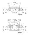
- FIG. 6 illustrates an image sensor package after flip chip (FC) mounting, in an embodiment.
- FC mounting may involve bonding solder 635 on pillar bump 633 to package contact pad 631 on package 620 .
- Discrete mount 630 may include a pillar bump 633 with solder 635 formed on the pillar bump 633 .
- FC mounting may generally refer to electrically coupling circuitry (not shown) on image sensor die 642 to circuitry (not shown) on package substrate 620 .
- An image sensor die 642 may be mounted on an image sensor carrier 643 . Circuitry on image sensor die 642 may be coupled to contact pads 637 using metal traces or bond wires (not shown) formed on image sensor carrier 643 .
- Image sensor die 642 may include an array of image pixels, as described above in connection with image pixel arrays 15 of FIG. 1 .
- Image sensor carrier 643 may have a plurality of contact pads 637 that are used to provide electrical connections to various electrical components on the image sensor die 642 via metal traces and/or bond wires (not shown) that may be formed on the image sensor carrier 643 .
- Image sensor normal vector 641 may indicate a direction normal to the plane of the chip carrier 643 and/or the image sensor die 642 .
- Package substrate 620 may be a printed circuit board made of glass fiber, or any other suitable laminate material such as FR-5 materials.
- Discrete mount 630 may include a pillar bump 633 with solder 635 formed on the pillar bump 633 .
- Pillar bump 633 may be formed from copper or any suitable electrically conductive material. Pillar bump 633 may be formed on a contact pad 637 of the image sensor carrier 643 , as shown in FIG. 6 .
- pillar bump 633 may be formed on a contact pad 631 of the package substrate 620 that is electrically coupled by metal traces and/or bond wires to other electrical components (not shown) that are mounted on substrate 620 .
- Ball mounts 690 may be formed on substrate 620 .
- Ball mounts 690 may be solder balls that are formed on a given side of the substrate 620 .
- Ball mounts 690 A are shown being formed on the same side of the substrate as the image sensor carrier 643 .
- Ball mounts 690 B are shown being formed on the opposite side of the substrate as the image sensor carrier 643 .
- Window 611 may be formed of glass, plastic, or any other suitable transparent material. Window 611 may be any transmittive element through which light can pass. Window 611 may be a lens element such as a field flattener lens. Window 611 may be a temporary element that is later removed. Window 611 is optional and may alternatively be omitted. In the embodiment of FIG. 6 , the dimensions of window 611 are about the same or slightly smaller than the dimensions of an opening in substrate 620 , similar to punch hole 524 of FIG. 5 . In other words, the opening in substrate 620 may have an area that is at least the same as the area of an image sensing region on the image sensor die 642 . Window normal vector 612 may indicate a direction normal to the plane of window 611 and/or substrate 620 .
- Window 611 may be attached to a lower surface of barrier structure 610 .
- the lower surface of barrier structure 610 may also be attached to the package substrate 620 . As shown in FIG. 6 , there may be a gap between window 611 and package substrate 620 . Alternatively, there may be no gap between window 611 and package substrate 620 .
- the lower surface of window 611 may be on the same plane as the lower surface of package substrate 620 .
- the upper surface of window 611 may be on the same plane as the upper surface of package substrate 620 .
- the window 611 may have the same thickness as the package substrate 620 .
- An upper surface of barrier structure 610 may be attached to image sensor carrier 643 .
- Barrier structure 610 may be formed of a dry film, or a B-stage epoxy resin, or any other material with similar dielectric properties.
- Thermal compression head 612 may be used to cure the material used in barrier structure 610 .
- Thermal compression head 612 may also be used to apply heat and/or pressure to chip carrier to properly package the image sensor. Heat produced from thermal compression head 612 may melt solder 635 and allow it to flow onto contact pad 631 , thereby electrically connecting contact pad 631 of the package substrate 620 with contact pad 637 of the image sensor carrier 643 .
- FIG. 6 shows thermal compression head 612 being positioned above image sensor carrier 643 ; however, thermal compression head 612 can alternatively be positioned on window 611 and/or substrate package 620 .
- Thermal compression head 612 may also be used to align image sensor normal vector 641 and window normal vector 612 so that they are parallel. Thermal compression head 612 may be able to apply a plurality of forces 615 on the image sensor carrier as shown in FIG. 6 . If thermal compression head 612 is positioned on window 611 and/or substrate 620 , then it may apply the same forces 615 to window 611 and/or substrate 620 . Thermal compression head may apply a left force 615 B to the image sensor carrier 643 to apply greater compressive force (or pressure) to the left side of the image sensor carrier 643 than to the right side of the image senor carrier 643 , during flip chip bonding or during any other stage of manufacturing the image sensor package of FIG. 6 .
- Applying left force 615 B may, in some cases, help align normal vectors image sensor normal vector 641 and window normal vector 612 . Applying left force 615 B may be appropriate when the angle between window normal vector 612 and image sensor normal vector 641 (as drawn) is less than 180 degrees with respect to the vector components in the plane of FIG. 6 .
- Thermal compression head may also apply a right force 615 C to the image sensor carrier 643 to apply greater compressive force (or pressure) to the right side of the image sensor carrier 643 than to the left side of the image senor carrier 643 , during flip chip bonding or during any other stage of manufacturing the image sensor package of FIG. 6 .
- Applying right force 615 C may, in some cases, help align normal vectors image sensor normal vector 641 and window normal 612 .
- Applying left force 615 B may be appropriate when the angle between window normal vector 612 and image sensor normal vector 641 (as drawn) is greater than 180 degrees with respect to the vector components in the plane of FIG. 6 .
- Thermal compression head may also apply a back/front/center force 615 A to the image sensor carrier 643 to apply a greater force to the back, front (in and out of the page of FIG. 6 , respectively) and center portions, respectively of image sensor carrier 643 than to other portions of the image sensor carrier 643 .
- Back/front/center forces 615 A may be applied during flip chip bonding or during any other stage of manufacturing the image sensor package of FIG. 6 . In general, the magnitude of any one of the forces 615 may be different than any other one of the forces 615 .
- underfill adhesive 650 may be deposited between discrete mounts 630 .
- Underfill adhesive 650 may be deposited on the substrate between gaps of the discrete mounts 630 .
- Underfill adhesive 650 may be deposited on the substrate after the solder 635 has been reflowed or melted to bond pillar bumps 633 to contact pads 637 of the image sensor carrier 243 . As described in connection with FIG. 4 above, underfill 650 will be blocked by barrier 610 and not be able to contaminate image sensor 642 or window 712 .
- FIG. 6 shows a single barrier structure 610 , which may be formed out of two separate barrier structures formed on image sensor carrier 643 and package substrate 620 as are barriers 510 A and 510 B respectively, in FIG. 5 . If two separate barrier structures are formed, it may be desirable if the height of the barrier structure formed on image sensor carrier 643 is greater than the height of the discrete mounts 630 .
- a barrier 610 may be a single structure that may be formed on either image sensor carrier 643 or package substrate 620 before being cured. It may be desirable that the height of the barrier 610 is greater than the height of the discrete mounts 630 .
- FIG. 7 illustrates an alternate embodiment of image sensor packaging in accordance with an embodiment.
- FC mounting may involve bonding solder 735 on pillar bump 733 to package contact pad 731 on package 720 .
- Discrete mount 730 may include a pillar bump 733 with solder 735 formed on the pillar bump 733 .
- FC mounting may generally refer to electrically coupling circuitry (not shown) on image sensor die 742 to circuitry (not shown) on package substrate 720 .
- An image sensor die 742 may be mounted on an image sensor carrier 743 . Circuitry on image sensor die 742 may be coupled to contact pads 737 using metal traces or bond wires (not shown) formed on image sensor carrier 743 .
- Image sensor die 742 may include an array of image pixels, as described above in connection with image pixel arrays 15 of FIG. 1 .
- Image sensor carrier 743 may have a plurality of contact pads 737 that are used to provide electrical connections to various electrical components on the image sensor die 742 via metal traces and/or bond wires (not shown) that may be formed on the image sensor carrier 743 .
- Image sensor normal vector 741 may indicate a direction normal to the plane of the chip carrier 743 and/or the image sensor die 742 .
- Package substrate 720 may be a printed circuit board made of glass fiber, or any other suitable laminate material such as FR-5 materials.
- Discrete mount 730 may include a pillar bump 733 with solder 735 formed on the pillar bump 733 .
- Pillar bump 733 may be formed from copper or any suitable electrically conductive material. Pillar bump 733 may be formed on a contact pad 731 of the package substrate 720 that is electrically coupled by metal traces and/or bond wires to other electrical components (not shown) that are mounted on substrate 720 , as shown in FIG. 7 .
- pillar bump 733 may be formed on a contact pad 737 of the image sensor carrier 743 .
- Ball mounts 790 may be formed on substrate 720 .
- Ball mounts 790 may be solder balls that are formed on a given side of the substrate 720 .
- Ball mounts 790 A are shown being formed on the same side of the substrate as the image sensor carrier 743 .
- Ball mounts 790 B are shown being formed on the opposite side of the substrate as the image sensor carrier 743 .
- Window 711 may be formed of glass, plastic, or any other suitable transparent material. Window 711 may be any transmittive element through which light can pass. Window 711 may be a lens element such as a field flattener lens. Window 711 may be a temporary element that is later removed. Window 711 is optional and may alternatively be omitted. In the embodiment of FIG. 7 , the dimensions of window 711 are greater than the dimensions of an opening in substrate 720 , similar to punch hole 524 of FIG. 5 . In other words, the opening in substrate 720 may have an area that is at least the same as the area of an image sensing region on the image sensor die 742 . Window normal vector 712 may indicate a direction normal to the plane of window 711 and/or substrate 720 .
- Window 711 may be attached to a lower surface of barrier structure 710 B. Window 711 may also be attached to the package substrate 720 by an adhesive layer 780 .
- Adhesive layer 780 may be a UV curable resin, a heat curable resin, an epoxy resin, or any other suitable adhesive.
- An upper surface of barrier structure 710 A may be attached to image sensor carrier 743 .
- Barrier structure 710 may be formed of a dry film, or a B-stage epoxy resin, or any other material with similar dielectric properties.
- Thermal compression head 712 may be used to cure the material used in barrier structure 710 .
- Thermal compression head 712 may also be used to apply heat and/or pressure to chip carrier to properly package the image sensor. Heat produced from thermal compression head 712 may melt solder 735 and allow it to flow onto contact pad 737 , thereby electrically connecting contact pad 731 of the package substrate 720 with contact pad 737 of the image sensor carrier 743 .
- FIG. 7 shows thermal compression head 712 being positioned above image sensor carrier 743 ; however, thermal compression head 712 can alternatively be positioned on window 711 and/or substrate package 720 .
- Thermal compression head 712 may also be used to align image sensor normal vector 741 and window normal vector 712 so that they are parallel. Thermal compression head 712 may be able to apply a plurality of forces 715 on the image sensor carrier as shown in FIG. 7 . If thermal compression head 712 is positioned on window 711 and/or substrate 720 , then it may apply the same forces 715 to window 711 and/or substrate 720 . Thermal compression head may apply a left force 715 B to the image sensor carrier 743 to apply greater compressive force (or pressure) to the left side of the image sensor carrier 743 than to the right side of the image senor carrier 743 , during flip chip bonding or during any other stage of manufacturing the image sensor package of FIG. 7 .
- Applying left force 715 B may, in some cases, help align normal vectors image sensor normal vector 741 and window normal vector 712 . Applying left force 715 B may be appropriate when the angle between window normal vector 712 and image sensor normal vector 741 (as drawn) is less than 0 degrees with respect to the vector components in the plane of FIG. 7 .
- Thermal compression head may also apply a right force 715 C to the image sensor carrier 743 to apply greater compressive force (or pressure) to the right side of the image sensor carrier 743 than to the left side of the image senor carrier 743 , during flip chip bonding or during any other stage of manufacturing the image sensor package of FIG. 7 .
- Applying right force 715 C may, in some cases, help align normal vectors image sensor normal vector 741 and window normal 712 .
- Applying left force 715 B may be appropriate when the angle between window normal vector 712 and image sensor normal vector 741 (as drawn) is greater than 0 degrees with respect to the vector components in the plane of FIG. 7 .
- Thermal compression head may also apply a back/front/center force 715 A to the image sensor carrier 743 to apply a greater force to the back, front (in and out of the page of FIG. 7 , respectively) and center portions, respectively of image sensor carrier 743 than to other portions of the image sensor carrier 743 .
- Back/front/center forces 715 A may be applied during flip chip bonding or during any other stage of manufacturing the image sensor package of FIG. 7 . In general, the magnitude of any one of the forces 715 may be different than any other one of the forces 715 .
- underfill adhesive 750 may be deposited between discrete mounts 730 . Underfill adhesive 750 may be deposited on the substrate between gaps of the discrete mounts 730 . Underfill adhesive 750 may be deposited on the substrate after the solder 735 has been reflowed or melted to bond pillar bumps 733 to contact pads 737 of the image sensor carrier 243 . As described in connection with FIG. 4 above, underfill 750 will be blocked by barrier 710 and not be able to contaminate image sensor 742 or window 712 .
- FIG. 7 shows two barrier structure 710 , namely 710 A and 710 B. Barriers 710 A and 710 B are shown having two different thicknesses. This is merely illustrative, as barriers 710 A and 710 B may have different thicknesses. Alternatively, a barrier 710 may be a single structure that may be formed on either image sensor carrier 743 or package substrate 720 before being cured.
- Barrier 710 A may have a first height h 4 whereas barrier 710 B may have a second height h 5 . The sum of these heights may be equal to the height h 6 . In some embodiments, it may be desirable for height h 4 of barrier structure 710 A to be greater than the height of the discrete mount 730 (not labeled).
- FIG. 8 is an illustrative flowchart of steps that may be used to create an image sensor package such as the embodiments of FIGS. 6 and 7 .
- steps 801 A and 805 A may be implemented to manufacture an image sensor package, without implementing steps 807 B and 813 B.
- steps 807 B and 813 B may be implemented, without implementing steps 801 A and 805 A.
- a barrier structure may be applied to an image sensor carrier, package substrate, and/or window in step 801 A.
- a barrier structure such as 610 or 710 A or may be applied to image sensor carrier 643 or 743 respectively.
- barriers 610 and 710 A may have a height that is greater than the height of a discrete mount such as 630 or 730 respectively.
- flip-chip bonding or mounting may occur. Solder such as 635 or 735 may be melted and flowed onto a contact pad such as 631 or 737 respectively.
- the contact pads 637 / 737 of the image sensor carrier 643 / 743 may be electrically connected to a respective contact pad 631 / 731 of the package substrate 620 / 720 .
- the electrical connection between contact pads 637 / 737 and 631 / 731 may be performed by heat reflow of solder on a pillar bump 633 / 733 , by ultrasonic bonding, or by thermosonic bonding of a gold stud bump (not illustrated).
- the normal vectors 612 / 712 and 641 / 741 may be aligned using combinations of forces 715 applied using thermal compression head 612 / 712 .
- underfill may be deposited between discrete mounts 630 / 730 .
- barrier structures such as 610 / 710 may prevent underfill adhesive from contaminating image sensor die 642 / 742 by virtue of having a height that is greater than the height of discrete mounts 630 / 730 .
- a window may be attached to the flip chip bonded package.
- a window 611 may be attached to a lower surface of barrier structure 610 .
- Adhesive may or may not be used to attach window 611 to the lower surface of barrier structure 610 .
- window 711 may be attached to a lower surface of barrier 710 B.
- window 711 may be attached to package substrate 720 using adhesive 780 which may be a UV cured adhesive, heat cured adhesive, epoxy resin, or any other suitable adhesive.
- Adhesive may or may not be used to attach window 711 to the lower surface of barrier structure 710 B.
- step 811 material of barrier structures 610 / 710 , which may be a dry film, B-stage epoxy resin, or any other material with similar dielectric properties may be cured.
- Adhesive such as the adhesive used to attach window 611 / 711 may also be cured.
- Thermal compression head 612 / 712 may be used to cure the barrier structures and/or adhesive.
- the normal vectors 612 / 712 and 641 / 741 may be aligned using combinations of forces 615 / 715 applied using thermal compression head 612 / 712 .
- flip-chip bonding or mounting may occur in step 803 .
- Solder such as 635 or 735 may be melted and flowed onto a contact pad such as 631 or 737 respectively.
- the contact pads 637 / 737 of the image sensor carrier 643 / 743 may be electrically connected to a respective contact pad 631 / 731 of the package substrate 620 / 720 .
- the electrical connection between contact pads 637 / 737 and 631 / 731 may be performed by heat reflow of solder on a pillar bump 633 / 733 , by ultrasonic bonding, or by thermosonic bonding of a gold stud bump (not illustrated).
- the normal vectors 612 / 712 and 641 / 741 may be aligned using combinations of forces 615 / 715 applied using thermal compression head 612 / 712 .
- a barrier structure may be applied to an image sensor carrier, package substrate, and/or window.
- a barrier structure such as 610 or 710 A or may be applied to image sensor carrier 643 or 743 respectively through a punch hole in substrate 620 / 720 such as punch hole 524 in substrate 520 of FIG. 5 .
- a window may be attached to the flip chip bonded package.
- a window 611 may be attached to a lower surface of barrier structure 610 .
- Adhesive may or may not be used to attach window 611 to the lower surface of barrier structure 610 .
- window 711 may be attached to a lower surface of barrier 710 B.
- window 711 may be attached to package substrate 720 using adhesive 780 which may be a UV cured adhesive, heat cured adhesive, epoxy resin, or any other suitable adhesive.
- Adhesive may or may not be used to attach window 711 to the lower surface of barrier structure 710 B.
- step 811 material of barrier structures 610 / 710 , which may be a dry film, B-stage epoxy resin, or any other material with similar dielectric properties may be cured.
- Adhesive such as the adhesive used to attach window 611 / 711 may also be cured.
- Thermal compression head 612 / 712 may be used to cure the barrier structures and/or adhesive.
- the normal vectors 612 / 712 and 641 / 741 may be aligned using combinations of forces 615 / 715 applied using thermal compression head 612 / 712 .
- underfill may be deposited between discrete mounts 630 / 730 .
- barrier structures such as 610 / 710 may prevent underfill adhesive from contaminating an image sensor die 642 / 742 as shown in FIG. 4 .
- FIG. 9 shows in simplified form a typical processor system 700 , such as a digital camera, which includes an imaging device such as imaging device 701 which may be, for example a multi-camera imaging system with one or more pixel arrays 716 .
- Device 701 may include the elements of system 900 ( FIG. 1 ) or any relevant subset of the elements.
- Processor system 700 is exemplary of a system having digital circuits that could include imaging device 701 . Without being limiting, such a system could include a computer system, still or video camera system, scanner, machine vision, vehicle navigation, video phone, surveillance system, auto focus system, star tracker system, motion detection system, image stabilization system, and other systems employing an imaging device.
- Processor system 700 may include a lens or multiple lenses indicated by lens 714 for focusing an image onto a pixel array or multiple pixel arrays such as a pixel array 716 when shutter release button 397 is pressed.
- Imaging device 701 may be a packaged image sensor as described in connection with FIGS. 6 and 7 .
- Processor system 700 may include a central processing unit such as central processing unit (CPU) 795 .
- CPU 795 may be a microprocessor that controls camera functions and one or more image flow functions and communicates with one or more input/output (I/O) devices 791 over a bus such as bus 793 .
- Imaging device 701 may also communicate with CPU 795 over bus 793 .
- System 700 may include random access memory (RAM) 792 and removable memory 794 .
- Removable memory 794 may include flash memory that communicates with CPU 795 over bus 793 .
- Imaging device 701 may be combined with CPU 795 , with or without memory storage, on a single integrated circuit or on a different chip.
- bus 793 is illustrated as a single bus, it may be one or more buses or bridges or other communication paths used to interconnect the system components.
- An image sensor package may include an image sensor carrier, an image sensor die, and a package substrate.
- An image sensor carrier may include a plurality of contact pads.
- An image sensor die may be attached to the image sensor carrier. Circuitry on the image sensor die may be coupled to the image sensor carrier contact pads via a plurality of metal interconnections such as metal traces or bond wires.
- a barrier structure may be formed on the image sensor carrier. The barrier structure may be formed out of B-stage resin, dry film, or any similar material. The barrier structure may surround the image sensor die and prevent contamination of the image sensor die by underfill adhesive and/or particles from the substrate or environment in which the image sensor is packaged.
- An image sensor carrier may be coupled to a package substrate.
- a plurality of discrete mount structures may be used to couple the image sensor carrier to the package substrate.
- the package substrate may include a plurality of contact pads coupled to circuitry on the package substrate via metal traces or bond wires.
- a given discrete mount structure may include pillar bumps or a stud bump. Pillar bumps may be used in discrete mount structures when the package substrate is bonded to the image sensor carrier using flip-chip bonding. Stud bumps may be used when the package substrate is bonded to the image sensor carrier using thermosonic bonding techniques.
- a window, or transparent structure may be included in an image sensor package.
- the package substrate may have a hole.
- the hole may have an area that is at least the same as the area of an image sensing region on the image sensor die.
- the transparent structure may be formed below the package substrate, or the transparent structure may be formed in the hole.
- the transparent structure may include a field flattener lens element.
- An adhesive may be used to attach the transparent structure to the package substrate.
- the transparent structure may be attached to at least a portion of a lower surface of the barrier that is opposite the surface of the barrier that is attached to the image sensor carrier. Another portion of the lower surface of the barrier may be attached to the package substrate.
- a thermal compression head may be used to attach or bond the package substrate to the image sensor carrier.
- the thermal compression head may also be used to cure adhesives in the image sensor package or to cure the barrier structure.
- the thermal compression head may be configured to varying forces on different portions of a surface, such as the surface of a window, the surface of a package substrate, and/or the surface of an image sensor carrier.
- the thermal compression head may be used to apply a force to first side of an image sensor that is greater than the force applied by the thermal compression head to second side of the image sensor that is opposite the first side.
- the thermal compression head may apply a greater force to any subset of the sides than to the remaining sides.
- the thermal compression head may be used to melt solder bumps on discrete mount structures.
- the thermal compression head may be used to melt stud bumps on discrete mount structures.
- the thermal compression head may be used in flip-chip bonding.
- the thermal compression head may be used to align vectors normal to the image sensor die and normal to the transparent structure.
- the barrier structure may be applied to the sensor carrier, package substrate, and/or window before or after flip-chip bonding the image sensor carrier to the package substrate via a plurality of discrete mounts.
- a window or transparent structure may be attached to the image sensor package.
- the transparent structure may be attached to the package substrate and/or to at least a portion of a lower surface of the barrier structure that is opposite an upper structure of the barrier structure that is attached to the image sensor carrier. Depositing underfill adhesive between discrete mounts may occur after flip chip bonding, before or after attaching the transparent structure to the package substrate.
- the barrier structure and/or adhesives in the image sensor package may be cured.
- the barrier structure and/or adhesives in the image sensor package may be cured using the thermal compression head.
Abstract
Description
Claims (15)
Priority Applications (1)
| Application Number | Priority Date | Filing Date | Title |
|---|---|---|---|
| US14/644,456 US9515108B2 (en) | 2015-03-11 | 2015-03-11 | Image sensors with contamination barrier structures |
Applications Claiming Priority (1)
| Application Number | Priority Date | Filing Date | Title |
|---|---|---|---|
| US14/644,456 US9515108B2 (en) | 2015-03-11 | 2015-03-11 | Image sensors with contamination barrier structures |
Publications (2)
| Publication Number | Publication Date |
|---|---|
| US20160268325A1 US20160268325A1 (en) | 2016-09-15 |
| US9515108B2 true US9515108B2 (en) | 2016-12-06 |
Family
ID=56886712
Family Applications (1)
| Application Number | Title | Priority Date | Filing Date |
|---|---|---|---|
| US14/644,456 Active 2035-04-27 US9515108B2 (en) | 2015-03-11 | 2015-03-11 | Image sensors with contamination barrier structures |
Country Status (1)
| Country | Link |
|---|---|
| US (1) | US9515108B2 (en) |
Cited By (1)
| Publication number | Priority date | Publication date | Assignee | Title |
|---|---|---|---|---|
| US20220020800A1 (en) * | 2020-07-15 | 2022-01-20 | Semiconductor Components Industries, Llc | Method for defining a gap height within an image sensor package |
Families Citing this family (5)
| Publication number | Priority date | Publication date | Assignee | Title |
|---|---|---|---|---|
| US10411152B2 (en) * | 2016-06-27 | 2019-09-10 | Merlin Solar Technologies, Inc. | Solar cell bonding |
| CN108074939A (en) * | 2017-12-15 | 2018-05-25 | 京东方科技集团股份有限公司 | Display base plate and preparation method thereof, display device |
| US20190219897A1 (en) * | 2018-01-17 | 2019-07-18 | Integrated Micro-Electronics, Inc. | Optically Aligned Camera Module Assembly Using Soldering |
| US20200052024A1 (en) * | 2018-08-10 | 2020-02-13 | Semiconductor Components Industries, Llc | Semiconductor sensors with charge dissipation layer and related methods |
| US11588994B2 (en) * | 2021-07-26 | 2023-02-21 | SmartSens Technology (HK) Co., Ltd | Image sensor with embedded neural processing unit |
Citations (9)
| Publication number | Priority date | Publication date | Assignee | Title |
|---|---|---|---|---|
| US5918363A (en) | 1996-05-20 | 1999-07-06 | Motorola, Inc. | Method for marking functional integrated circuit chips with underfill material |
| US5942798A (en) | 1997-11-24 | 1999-08-24 | Stmicroelectronics, Inc. | Apparatus and method for automating the underfill of flip-chip devices |
| US6214635B1 (en) | 1996-03-07 | 2001-04-10 | Micron Technology, Inc. | Method and apparatus for underfill of bumped or raised die |
| US20090273094A1 (en) * | 2008-05-02 | 2009-11-05 | Jong-Woo Ha | Integrated circuit package on package system |
| US20090321863A1 (en) * | 2008-06-25 | 2009-12-31 | Micron Technology, Inc. | Method and apparatus providing an imager module with a permanent carrier |
| US20100200898A1 (en) * | 2009-02-11 | 2010-08-12 | Megica Corporation | Image and light sensor chip packages |
| US20130028589A1 (en) * | 2011-07-25 | 2013-01-31 | Pai-Chun Peter Zung | Compact camera module and method for fabricating the same |
| US20130221470A1 (en) * | 2012-02-29 | 2013-08-29 | Larry D. Kinsman | Multi-chip package for imaging systems |
| US20130270230A1 (en) | 2012-04-17 | 2013-10-17 | Yiu Ming Cheung | Thermal compression bonding of semiconductor chips |
-
2015
- 2015-03-11 US US14/644,456 patent/US9515108B2/en active Active
Patent Citations (9)
| Publication number | Priority date | Publication date | Assignee | Title |
|---|---|---|---|---|
| US6214635B1 (en) | 1996-03-07 | 2001-04-10 | Micron Technology, Inc. | Method and apparatus for underfill of bumped or raised die |
| US5918363A (en) | 1996-05-20 | 1999-07-06 | Motorola, Inc. | Method for marking functional integrated circuit chips with underfill material |
| US5942798A (en) | 1997-11-24 | 1999-08-24 | Stmicroelectronics, Inc. | Apparatus and method for automating the underfill of flip-chip devices |
| US20090273094A1 (en) * | 2008-05-02 | 2009-11-05 | Jong-Woo Ha | Integrated circuit package on package system |
| US20090321863A1 (en) * | 2008-06-25 | 2009-12-31 | Micron Technology, Inc. | Method and apparatus providing an imager module with a permanent carrier |
| US20100200898A1 (en) * | 2009-02-11 | 2010-08-12 | Megica Corporation | Image and light sensor chip packages |
| US20130028589A1 (en) * | 2011-07-25 | 2013-01-31 | Pai-Chun Peter Zung | Compact camera module and method for fabricating the same |
| US20130221470A1 (en) * | 2012-02-29 | 2013-08-29 | Larry D. Kinsman | Multi-chip package for imaging systems |
| US20130270230A1 (en) | 2012-04-17 | 2013-10-17 | Yiu Ming Cheung | Thermal compression bonding of semiconductor chips |
Cited By (2)
| Publication number | Priority date | Publication date | Assignee | Title |
|---|---|---|---|---|
| US20220020800A1 (en) * | 2020-07-15 | 2022-01-20 | Semiconductor Components Industries, Llc | Method for defining a gap height within an image sensor package |
| US11869912B2 (en) * | 2020-07-15 | 2024-01-09 | Semiconductor Components Industries, Llc | Method for defining a gap height within an image sensor package |
Also Published As
| Publication number | Publication date |
|---|---|
| US20160268325A1 (en) | 2016-09-15 |
Similar Documents
| Publication | Publication Date | Title |
|---|---|---|
| US9515108B2 (en) | Image sensors with contamination barrier structures | |
| US9041840B2 (en) | Backside illuminated image sensors with stacked dies | |
| US11043436B2 (en) | Semiconductor device, manufacturing method, imaging device, and electronic apparatus for enabling component mounting with high flatness | |
| TWI686937B (en) | Methods of forming image sensor integrated circuit packages | |
| US7675131B2 (en) | Flip-chip image sensor packages and methods of fabricating the same | |
| US20090206431A1 (en) | Imager wafer level module and method of fabrication and use | |
| US8975583B2 (en) | 3D stacked uncooled IR sensor device and method | |
| CN109585471B (en) | Semiconductor package and image sensor | |
| US10446598B2 (en) | Semiconductor device, manufacturing method, and electronic apparatus | |
| US9281335B2 (en) | Alignment marks and alignment methods for aligning backside components to frontside components in integrated circuits | |
| US9368535B2 (en) | Imaging systems with flip chip ball grid arrays | |
| US20120281113A1 (en) | USING A MULTI-CHIP SYSTEM IN A PACKAGE (MCSiP) IN IMAGING APPLICATIONS TO YIELD A LOW COST, SMALL SIZE CAMERA ON A CHIP | |
| US9865641B2 (en) | Solid-state imaging device, manufacturing method therefor, and imaging apparatus | |
| WO2015122299A1 (en) | Solid-state imaging device, electronic apparatus, and solid-state imaging device manufacturing method | |
| KR102172437B1 (en) | Camera module | |
| TWI812908B (en) | Image sensor package | |
| KR102396490B1 (en) | Camera packaging apparatus including semiconductor | |
| KR102396489B1 (en) | Camera packaging apparatus | |
| KR20230166441A (en) | A camera module and optical apparatus having the same | |
| Humpston | Wafer-level packaging of image sensors |
Legal Events
| Date | Code | Title | Description |
|---|---|---|---|
| AS | Assignment |
Owner name: SEMICONDUCTOR COMPONENTS INDUSTRIES, LLC, ARIZONA Free format text: ASSIGNMENT OF ASSIGNORS INTEREST;ASSIGNORS:HSIEH, YU-TE;WU, WEN-JIN;REEL/FRAME:035137/0355 Effective date: 20150311 |
|
| AS | Assignment |
Owner name: DEUTSCHE BANK AG NEW YORK BRANCH, NEW YORK Free format text: SECURITY INTEREST;ASSIGNOR:SEMICONDUCTOR COMPONENTS INDUSTRIES, LLC;REEL/FRAME:038620/0087 Effective date: 20160415 |
|
| AS | Assignment |
Owner name: DEUTSCHE BANK AG NEW YORK BRANCH, AS COLLATERAL AG Free format text: CORRECTIVE ASSIGNMENT TO CORRECT THE INCORRECT PATENT NUMBER 5859768 AND TO RECITE COLLATERAL AGENT ROLE OF RECEIVING PARTY IN THE SECURITY INTEREST PREVIOUSLY RECORDED ON REEL 038620 FRAME 0087. ASSIGNOR(S) HEREBY CONFIRMS THE SECURITY INTEREST;ASSIGNOR:SEMICONDUCTOR COMPONENTS INDUSTRIES, LLC;REEL/FRAME:039853/0001 Effective date: 20160415 Owner name: DEUTSCHE BANK AG NEW YORK BRANCH, AS COLLATERAL AGENT, NEW YORK Free format text: CORRECTIVE ASSIGNMENT TO CORRECT THE INCORRECT PATENT NUMBER 5859768 AND TO RECITE COLLATERAL AGENT ROLE OF RECEIVING PARTY IN THE SECURITY INTEREST PREVIOUSLY RECORDED ON REEL 038620 FRAME 0087. ASSIGNOR(S) HEREBY CONFIRMS THE SECURITY INTEREST;ASSIGNOR:SEMICONDUCTOR COMPONENTS INDUSTRIES, LLC;REEL/FRAME:039853/0001 Effective date: 20160415 |
|
| STCF | Information on status: patent grant |
Free format text: PATENTED CASE |
|
| MAFP | Maintenance fee payment |
Free format text: PAYMENT OF MAINTENANCE FEE, 4TH YEAR, LARGE ENTITY (ORIGINAL EVENT CODE: M1551); ENTITY STATUS OF PATENT OWNER: LARGE ENTITY Year of fee payment: 4 |
|
| AS | Assignment |
Owner name: FAIRCHILD SEMICONDUCTOR CORPORATION, ARIZONA Free format text: RELEASE OF SECURITY INTEREST IN PATENTS RECORDED AT REEL 038620, FRAME 0087;ASSIGNOR:DEUTSCHE BANK AG NEW YORK BRANCH, AS COLLATERAL AGENT;REEL/FRAME:064070/0001 Effective date: 20230622 Owner name: SEMICONDUCTOR COMPONENTS INDUSTRIES, LLC, ARIZONA Free format text: RELEASE OF SECURITY INTEREST IN PATENTS RECORDED AT REEL 038620, FRAME 0087;ASSIGNOR:DEUTSCHE BANK AG NEW YORK BRANCH, AS COLLATERAL AGENT;REEL/FRAME:064070/0001 Effective date: 20230622 |