US9507250B2 - Optical proximity correction for improved electrical characteristics - Google Patents

Optical proximity correction for improved electrical characteristics Download PDF

Info

Publication number
US9507250B2
US9507250B2 US12/640,166 US64016609A US9507250B2 US 9507250 B2 US9507250 B2 US 9507250B2 US 64016609 A US64016609 A US 64016609A US 9507250 B2 US9507250 B2 US 9507250B2
Authority
US
United States
Prior art keywords
group
segments
computer
segment
adjusting positions
Prior art date
Legal status (The legal status is an assumption and is not a legal conclusion. Google has not performed a legal analysis and makes no representation as to the accuracy of the status listed.)
Expired - Fee Related, expires
Application number
US12/640,166
Other versions
US20110154271A1 (en
Inventor
Kanak B. Agarwal
Sani R. Nassif
Current Assignee (The listed assignees may be inaccurate. Google has not performed a legal analysis and makes no representation or warranty as to the accuracy of the list.)
International Business Machines Corp
Original Assignee
International Business Machines Corp
Priority date (The priority date is an assumption and is not a legal conclusion. Google has not performed a legal analysis and makes no representation as to the accuracy of the date listed.)
Filing date
Publication date
Application filed by International Business Machines Corp filed Critical International Business Machines Corp
Priority to US12/640,166 priority Critical patent/US9507250B2/en
Assigned to INTERNATIONAL BUSINESS MACHINES CORPORATION reassignment INTERNATIONAL BUSINESS MACHINES CORPORATION ASSIGNMENT OF ASSIGNORS INTEREST (SEE DOCUMENT FOR DETAILS). Assignors: AGARWAL, KANAK B, NASSIF, SANI R
Publication of US20110154271A1 publication Critical patent/US20110154271A1/en
Application granted granted Critical
Publication of US9507250B2 publication Critical patent/US9507250B2/en
Expired - Fee Related legal-status Critical Current
Adjusted expiration legal-status Critical

Links

Images

Classifications

    • G03F1/144
    • GPHYSICS
    • G03PHOTOGRAPHY; CINEMATOGRAPHY; ANALOGOUS TECHNIQUES USING WAVES OTHER THAN OPTICAL WAVES; ELECTROGRAPHY; HOLOGRAPHY
    • G03FPHOTOMECHANICAL PRODUCTION OF TEXTURED OR PATTERNED SURFACES, e.g. FOR PRINTING, FOR PROCESSING OF SEMICONDUCTOR DEVICES; MATERIALS THEREFOR; ORIGINALS THEREFOR; APPARATUS SPECIALLY ADAPTED THEREFOR
    • G03F1/00Originals for photomechanical production of textured or patterned surfaces, e.g., masks, photo-masks, reticles; Mask blanks or pellicles therefor; Containers specially adapted therefor; Preparation thereof
    • G03F1/36Masks having proximity correction features; Preparation thereof, e.g. optical proximity correction [OPC] design processes

Definitions

  • the present invention relates generally to computer-aided design of photolithographic masks used in the manufacturing of integrated circuits. More specifically, the present invention is directed to an improved method, computer program product, and apparatus for performing optical proximity correction in such masks.
  • Integrated circuits are commonly manufactured through a photolithographic process.
  • photolithography a layer of light-sensitive material (photoresist) is applied atop a layer of material to be etched by the process.
  • a geometric pattern is applied to the photoresist by shining light of a prescribed wavelength through a photolithographic mask (also referred to as a “photomask” or, simply, “mask”) containing the pattern.
  • a photomask is an opaque plate with holes or transparencies that allow light to shine through in a defined pattern.
  • region of transparency shall be used to denote either a hole in the plate or an actual transparent portion of the plate, so that a single term may be used to refer to either possibility.
  • a “region of opacity” shall be used to denote an opaque feature in the photomask.
  • the term “region” shall be used to denote either a region of transparency or a region of opacity.
  • lithographic photomasks are typically transparent fused silica blanks covered with a pattern defined with a chrome metal absorbing film. They are typically manufactured to a size that is substantially larger than that of the circuit itself, and reduction optics are used to project the mask pattern onto the photoresist at the correct size. The light passing through the mask causes changes to occur in the photoresist such that a subsequent etching process leaves selected portions of the photoresist and immediately underlying material layer intact, while removing undesired portions of such layers.
  • photolithography can be used to define the geometric pattern of the polysilicon layer in a MOS (metal-oxide semiconductor) integrated circuit technology (the layer in which the gates of MOSFETs [metal-oxide semiconductor field-effect transistors] are defined).
  • MOS metal-oxide semiconductor
  • FIG. 1 depicts the IC layout of a simple MOSFET 100 .
  • MOSFET 100 is made up of a region of doped silicon 102 (either N-type or P-type) overlapped by a region of polysilicon material 104 .
  • the gate of the transistor is defined by the rectangular portion ( 106 ) of polysilicon region 104 that overlaps doped silicon region 102 .
  • the electrical behavior of the MOSFET thus constructed is modeled by a parameter “K,” which is directly proportional to the ratio of the width ( 108 ) of gate 106 to its length ( 110 ).
  • K the relative dimensions of transistor features are critical to the proper electrical behavior of a given device.
  • the minimum feature sizes available in a given technology are limited, at least in part, by the nature of the photolithographic process itself. Specifically, as feature sizes approach the wavelengths of light used in the process (e.g., at sub-micron feature sizes for conventional photolithography using ultraviolet light), diffraction (a result of the wave-nature of electromagnetic radiation) reduces the fidelity of the image projected onto the photoresist.
  • a rectilinear feature 200 in a photomask existing either as a region of transparency or as a region of opacity
  • FIG. 2 might be rendered in a distorted curvilinear shape (such as shape 300 ) in the photoresist, as depicted in FIG. 3 .
  • OPC optical proximity correction
  • an OPC-modified version 400 of mask pattern 200 is depicted, wherein irregularities (e.g., irregularities 402 and 404 ) are introduced into the mask shape so as to counteract the distortions caused by diffraction.
  • OPC relies on computerized optimization algorithms to minimize “edge placement error” (EPE).
  • EPE is a metric that represents the distance between a location on the projected image and a corresponding location in the mask pattern. In a typical implementation, modifications to the mask pattern are made using a gradient-descent approach to minimize the overall EPE of a mask pattern.
  • EPE-based OPC is a useful technique
  • the results obtained from such technique are not necessarily optimal in the sense of electrical behavior. More specifically, although the projected image may better conform to the desired shape, the electrical behavior of the resulting device may differ substantially from what is desired, thus necessitating complex electrical simulation and further adjustment of the mask pattern in response.
  • the present invention provides a solution to this and other problems, and offers other advantages over previous solutions.
  • the present invention provides a method, computer program product, and data processing system for performing an improved optical proximity correction that better respects the electrical properties of the device being manufactured.
  • the present invention recognizes that the electrical properties of a given device are a function of its dimensions (size), as opposed to its edge positions (shape).
  • a preferred embodiment of the present invention performs OPC by first dividing the perimeter of a mask region in an integrated circuit into a plurality of segments, then grouping the segments into at least two distinct groups, wherein segments in the first of these groups are adjusted in position so as to minimize edge placement error (EPE) when the photolithography using the mask is simulated.
  • EPE edge placement error
  • Segments in the second group are adjusted in position so as to minimize cumulative error in a dimension spanning the region, wherein the span of such dimension extends from segments in the first group to segments in the second group.
  • Optical Proximity Correction so obtained by this process, because such correction is obtained with reference to desired dimensions, as opposed to merely position, more readily preserves the intended electrical behavior of the device as originally designed (before the correction took place).
  • FIG. 1 is a diagram illustrating the silicon layout of a simple MOSFET
  • FIG. 2 is a diagram illustrating an exemplary rectilinear region in a photomask
  • FIG. 3 is a diagram illustrating diffraction-induced distortions in the projected image obtained from a photomask at the sub-micron level
  • FIG. 4 is a diagram of an exemplary region in a photomask design that is a possible result of applying optical proximity correction (OPC) to the photomask design in FIG. 2 ;
  • OPC optical proximity correction
  • FIG. 5 is a diagram illustrating a step of dividing a perimeter of a region into a plurality of segments and further grouping those segments for electrically-motivated optical proximity correction in accordance with a preferred embodiment of the present invention
  • FIG. 6 is a diagram illustrating a step of preparing various modified versions of a region for the purpose of simulating the effects of various segment adjustments in accordance with a preferred embodiment of the present invention
  • FIG. 7 is a flowchart representation of a process of performing electrically-motivated optical proximity correction in accordance with a preferred embodiment of the present invention.
  • FIG. 8 is a diagram of a data processing system in which a preferred embodiment of the present invention may be implemented.
  • a preferred embodiment of the present invention is illustrated with respect to an exemplary feature or “region” 502 in a photomask pattern.
  • region 502 For the purpose of this example, a purely rectangular region is selected, which would be representative of a simple polysilicon layer utilized to form the gate of a single MOSFET, such as MOSFET 100 in FIG. 1 .
  • the process of performing optical proximity correction in this preferred embodiment of the invention begins with the division of the perimeter of region 502 into a plurality of segments, such as segment 504 . These segments are then grouped into two groups, shown here as group 506 and group 508 . One of these groups (we will choose group 506 in this example) will have the positions of its segments adjusted as to minimize edge placement error (EPE), whereas the other group (group 508 ) will have the positions of its segments adjusted so as to minimize dimensional error.
  • EPE edge placement error
  • segment 602 is a segment that is to be adjusted for minimal edge placement error (EPE) because it belongs to group 506 (as shown in the previous figure)—we will refer to this type of adjustment as “edge-optimization.”
  • EPE minimal edge placement error
  • a photolithography simulation is first performed on region 502 to obtain a simulated printed contour 612 . If the printed contour generated from the simulation (contour 612 ) is within the boundary of the desired shape (as shown in FIG. 6 ), segment 602 is displaced outward, thus replacing segment 602 with an outwardly extending serif 604 .
  • segment 602 would instead be replaced with a concave notch 608 .
  • the size of the notch or serif generated, in either case, is computed as a function of the magnitude of the edge placement error of segment 602 (so that greater errors result in greater displacements, for instance).
  • the same simulation data is used for the segments in group 508 (for example, segment 610 ).
  • the choice of positional adjustment is made not for the purpose of minimizing EPE, but for the purpose of minimizing the dimensional error for each segment.
  • the dimensional error at a single point would, in a preferred embodiment, be the difference between width 618 (the width of the desired shape at that point) and width 616 (the width of the simulated shape at the same point). If the dimensional error for segment 610 , for example, indicates that the printed contour is too narrow between segment 602 and segment 610 , segment 610 can be replaced with a convex serif. If the contour is too wide, on the other hand, segment 610 can be replaced with a concave notch. As with the EPE-optimized segments, the size of each notch or serif created is a function of the magnitude of the error associated with that segment.
  • FIG. 7 This overall process is depicted in more complete detail in FIG. 7 , where it is presented in flowchart form.
  • the perimeter of that region is divided into a plurality of segments (block 700 ). These segments are then grouped into “edge-optimized” and “dimension-optimized” groups (block 702 ).
  • the photolithographic process is simulated on the current mask (block 704 ) and an EPE score and dimensional error score are computed from this simulation (block 706 ). If these error scores are acceptable (i.e., there is no more than an acceptable level of overall error), the process terminated (block 708 : No), but if the error scores exceed acceptable levels, the process continues to consider each segment in the region individually.
  • next segment in the region is examined (block 710 ). A determination is then made as to whether the segment is to be “edge-optimized.” If so (block 714 : Yes), then the “error” score for each displacement is calculated as the EPE score for that displacement (block 716 ). If not, however, (block 714 : No), the “error” score for each displacement is calculated as the dimensional error score for that displacement (block 718 ).
  • a displacement that reduces the “error” score (either EPE or displacement, depending on context) for that segment is then computed on the basis of the determined error and the photomask design adjusted according to that choice (block 720 ). If there are more segments in the region to be considered (block 722 : Yes), the process loops back to block 710 to consider the next segment. If not (block 722 : No), the process returns to block 704 to determine the over all acceptability of the design as modified.
  • a gradient-descent search method may be used to optimize the mask according to global objective functions.
  • simulations are run for different displacements (inward or outward) and the displacement that, according to the simulation, minimizes the overall EPE or dimensional error (depending on the segment in question) is chosen.
  • FIG. 8 illustrates information handling system 801 which is a simplified example of a computer system/data processing system capable of performing the computing operations described herein with respect to a preferred embodiment of the present invention.
  • Computer system 801 includes processor 800 which is coupled to host bus 802 .
  • a level two (L2) cache memory 804 is also coupled to host bus 802 .
  • Host-to-PCI bridge 806 is coupled to main memory 808 , includes cache memory and main memory control functions, and provides bus control to handle transfers among PCI bus 810 , processor 800 , L2 cache 804 , main memory 808 , and host bus 802 .
  • Main memory 808 is coupled to Host-to-PCI bridge 806 as well as host bus 802 .
  • PCI bus 810 Devices used solely by host processor(s) 800 , such as LAN card 830 , are coupled to PCI bus 810 .
  • Service Processor Interface and ISA Access Pass-through 812 provides an interface between PCI bus 810 and PCI bus 814 .
  • PCI bus 814 is insulated from PCI bus 810 .
  • Devices, such as flash memory 818 are coupled to PCI bus 814 .
  • flash memory 818 includes BIOS code that incorporates the necessary processor executable code for a variety of low-level system functions and system boot functions.
  • PCI bus 814 provides an interface for a variety of devices that are shared by host processor(s) 800 and Service Processor 816 including, for example, flash memory 818 .
  • PCI-to-ISA bridge 835 provides bus control to handle transfers between PCI bus 814 and ISA bus 840 , universal serial bus (USB) functionality 845 , power management functionality 855 , and can include other functional elements not shown, such as a real-time clock (RTC), DMA control, interrupt support, and system management bus support.
  • RTC real-time clock
  • Nonvolatile RAM 820 is attached to ISA Bus 840 .
  • Service Processor 816 includes JTAG and I2C buses 822 for communication with processor(s) 800 during initialization steps.
  • JTAG/I2C buses 822 are also coupled to L2 cache 804 , Host-to-PCI bridge 806 , and main memory 808 providing a communications path between the processor, the Service Processor, the L2 cache, the Host-to-PCI bridge, and the main memory.
  • Service Processor 816 also has access to system power resources for powering down information handling device 801 .
  • Peripheral devices and input/output (I/O) devices can be attached to various interfaces (e.g., parallel interface 862 , serial interface 864 , keyboard interface 868 , and mouse interface 870 coupled to ISA bus 840 .
  • USB hub 845 for instance, is shown connected to a media reader 846 for the purpose of reading machine-readable tangible data storage media, e.g., data storage medium 846 A, such as memory cards, optical discs, and the like.
  • a super I/O controller (not shown) attached to ISA bus 840 .
  • LAN card 830 is coupled to PCI bus 810 .
  • modem 875 is connected to serial port 864 and PCI-to-ISA Bridge 835 .
  • FIG. 8 While the computer system described in FIG. 8 is capable of executing the processes described herein, this computer system is simply one example of a computer system. Those skilled in the art will appreciate that many other computer system designs are capable of performing the processes described herein.
  • One of the preferred implementations of the invention is a computer program, namely, a set of instructions (program code) or other functional descriptive material in a code module that may, for example, be resident in the random access memory of the computer.
  • the set of instructions may be stored in another computer memory, for example, in a hard disk drive, or in a removable memory such as an optical disk (for eventual use in a CD ROM) or floppy disk (for eventual use in a floppy disk drive), e.g., computer program product 846 B in data storage medium 846 A, or downloaded via the Internet or other computer network.
  • the present invention may be implemented as a computer program product for use in a computer.

Abstract

A method, computer program product, and data processing system for performing an improved optical proximity correction are disclosed, which better respect the electrical properties of the device being manufactured. A preferred embodiment of the present invention performs OPC by first dividing the perimeter of a mask region into a plurality of segments, then grouping the segments into at least two distinct groups, wherein segments in the first of these groups are adjusted in position so as to minimize edge placement error (EPE) when the photolithography using the mask is simulated. Segments in the second group are adjusted in position so as to minimize cumulative error in a dimension spanning the region, wherein the span of such dimension extends from segments in the first group to segments in the second group. Correction so obtained by this process more readily preserves the intended electrical behavior of the original device design.

Description

BACKGROUND OF THE INVENTION
1. Technical Field
The present invention relates generally to computer-aided design of photolithographic masks used in the manufacturing of integrated circuits. More specifically, the present invention is directed to an improved method, computer program product, and apparatus for performing optical proximity correction in such masks.
2. Description of the Related Art
Integrated circuits (ICs) are commonly manufactured through a photolithographic process. In photolithography, a layer of light-sensitive material (photoresist) is applied atop a layer of material to be etched by the process. A geometric pattern is applied to the photoresist by shining light of a prescribed wavelength through a photolithographic mask (also referred to as a “photomask” or, simply, “mask”) containing the pattern. A photomask is an opaque plate with holes or transparencies that allow light to shine through in a defined pattern. (Henceforth herein, the term “region of transparency” shall be used to denote either a hole in the plate or an actual transparent portion of the plate, so that a single term may be used to refer to either possibility. A “region of opacity” shall be used to denote an opaque feature in the photomask. The term “region” shall be used to denote either a region of transparency or a region of opacity.) In practice, lithographic photomasks are typically transparent fused silica blanks covered with a pattern defined with a chrome metal absorbing film. They are typically manufactured to a size that is substantially larger than that of the circuit itself, and reduction optics are used to project the mask pattern onto the photoresist at the correct size. The light passing through the mask causes changes to occur in the photoresist such that a subsequent etching process leaves selected portions of the photoresist and immediately underlying material layer intact, while removing undesired portions of such layers. For example, photolithography can be used to define the geometric pattern of the polysilicon layer in a MOS (metal-oxide semiconductor) integrated circuit technology (the layer in which the gates of MOSFETs [metal-oxide semiconductor field-effect transistors] are defined).
FIG. 1, for example, depicts the IC layout of a simple MOSFET 100. MOSFET 100 is made up of a region of doped silicon 102 (either N-type or P-type) overlapped by a region of polysilicon material 104. The gate of the transistor is defined by the rectangular portion (106) of polysilicon region 104 that overlaps doped silicon region 102. In the standard Shichman-Hodges MOSFET model, the electrical behavior of the MOSFET thus constructed is modeled by a parameter “K,” which is directly proportional to the ratio of the width (108) of gate 106 to its length (110). Thus, the relative dimensions of transistor features are critical to the proper electrical behavior of a given device.
The minimum feature sizes available in a given technology are limited, at least in part, by the nature of the photolithographic process itself. Specifically, as feature sizes approach the wavelengths of light used in the process (e.g., at sub-micron feature sizes for conventional photolithography using ultraviolet light), diffraction (a result of the wave-nature of electromagnetic radiation) reduces the fidelity of the image projected onto the photoresist. For example, a rectilinear feature 200 in a photomask (existing either as a region of transparency or as a region of opacity), as depicted in FIG. 2, might be rendered in a distorted curvilinear shape (such as shape 300) in the photoresist, as depicted in FIG. 3.
One potential way of dealing with this problem is to shorten the wavelengths of light used. Thus, the use of extremely short-wavelength ultraviolet radiation or X-ray radiation for photolithography is a topic of current research. Another method of dealing with this problem is to employ what has come to be known as optical proximity correction (OPC). In OPC, diffusion-induced distortions in the pattern applied to the photoresist are reduced in severity by introducing small irregularities into the mask itself. The effect of these irregularities is to “predistort” the mask pattern in such a way that the diffraction-induced distortions are minimized. For example, in FIG. 4, an OPC-modified version 400 of mask pattern 200 is depicted, wherein irregularities (e.g., irregularities 402 and 404) are introduced into the mask shape so as to counteract the distortions caused by diffraction. OPC, as it is practiced in the art, relies on computerized optimization algorithms to minimize “edge placement error” (EPE). EPE is a metric that represents the distance between a location on the projected image and a corresponding location in the mask pattern. In a typical implementation, modifications to the mask pattern are made using a gradient-descent approach to minimize the overall EPE of a mask pattern.
Although EPE-based OPC is a useful technique, the results obtained from such technique are not necessarily optimal in the sense of electrical behavior. More specifically, although the projected image may better conform to the desired shape, the electrical behavior of the resulting device may differ substantially from what is desired, thus necessitating complex electrical simulation and further adjustment of the mask pattern in response.
What is needed, therefore, is a method of performing optical proximity correction which respects the electrical properties of the device being manufactured. The present invention provides a solution to this and other problems, and offers other advantages over previous solutions.
SUMMARY OF THE INVENTION
Accordingly, the present invention provides a method, computer program product, and data processing system for performing an improved optical proximity correction that better respects the electrical properties of the device being manufactured. Specifically, the present invention recognizes that the electrical properties of a given device are a function of its dimensions (size), as opposed to its edge positions (shape). In particular, a preferred embodiment of the present invention performs OPC by first dividing the perimeter of a mask region in an integrated circuit into a plurality of segments, then grouping the segments into at least two distinct groups, wherein segments in the first of these groups are adjusted in position so as to minimize edge placement error (EPE) when the photolithography using the mask is simulated. Segments in the second group are adjusted in position so as to minimize cumulative error in a dimension spanning the region, wherein the span of such dimension extends from segments in the first group to segments in the second group. Optical Proximity Correction so obtained by this process, because such correction is obtained with reference to desired dimensions, as opposed to merely position, more readily preserves the intended electrical behavior of the device as originally designed (before the correction took place).
The foregoing is a summary and thus contains, by necessity, simplifications, generalizations, and omissions of detail; consequently, those skilled in the art will appreciate that the summary is illustrative only and is not intended to be in any way limiting. Other aspects, inventive features, and advantages of the present invention, as defined solely by the claims, will become apparent in the non-limiting detailed description set forth below.
BRIEF DESCRIPTION OF THE DRAWINGS
The present invention may be better understood, and its numerous objects, features, and advantages made apparent to those skilled in the art by referencing the accompanying drawings, wherein:
FIG. 1 is a diagram illustrating the silicon layout of a simple MOSFET;
FIG. 2 is a diagram illustrating an exemplary rectilinear region in a photomask;
FIG. 3 is a diagram illustrating diffraction-induced distortions in the projected image obtained from a photomask at the sub-micron level;
FIG. 4 is a diagram of an exemplary region in a photomask design that is a possible result of applying optical proximity correction (OPC) to the photomask design in FIG. 2;
FIG. 5 is a diagram illustrating a step of dividing a perimeter of a region into a plurality of segments and further grouping those segments for electrically-motivated optical proximity correction in accordance with a preferred embodiment of the present invention;
FIG. 6 is a diagram illustrating a step of preparing various modified versions of a region for the purpose of simulating the effects of various segment adjustments in accordance with a preferred embodiment of the present invention;
FIG. 7 is a flowchart representation of a process of performing electrically-motivated optical proximity correction in accordance with a preferred embodiment of the present invention; and
FIG. 8 is a diagram of a data processing system in which a preferred embodiment of the present invention may be implemented.
DETAILED DESCRIPTION
The following is intended to provide a detailed description of an example of the invention and should not be taken to be limiting of the invention itself. Rather, any number of variations may fall within the scope of the invention, which is defined in the claims following the description.
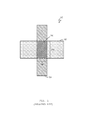
Operation of a preferred embodiment of the present invention is illustrated with respect to an exemplary feature or “region” 502 in a photomask pattern. For the purpose of this example, a purely rectangular region is selected, which would be representative of a simple polysilicon layer utilized to form the gate of a single MOSFET, such as MOSFET 100 in FIG. 1. The process of performing optical proximity correction in this preferred embodiment of the invention begins with the division of the perimeter of region 502 into a plurality of segments, such as segment 504. These segments are then grouped into two groups, shown here as group 506 and group 508. One of these groups (we will choose group 506 in this example) will have the positions of its segments adjusted as to minimize edge placement error (EPE), whereas the other group (group 508) will have the positions of its segments adjusted so as to minimize dimensional error.
The actual process of determining which corrections to make to region 502 is illustrated in FIG. 6. Each segment is considered individually in this process. In this example, we will start with segment 602, which is a segment that is to be adjusted for minimal edge placement error (EPE) because it belongs to group 506 (as shown in the previous figure)—we will refer to this type of adjustment as “edge-optimization.” To perform the adjustment, a photolithography simulation is first performed on region 502 to obtain a simulated printed contour 612. If the printed contour generated from the simulation (contour 612) is within the boundary of the desired shape (as shown in FIG. 6), segment 602 is displaced outward, thus replacing segment 602 with an outwardly extending serif 604. In the opposite case, where the simulation contour extends outside of the boundary of the desired shape, segment 602 would instead be replaced with a concave notch 608. The size of the notch or serif generated, in either case, is computed as a function of the magnitude of the edge placement error of segment 602 (so that greater errors result in greater displacements, for instance).
For the segments in group 508 (for example, segment 610), the same simulation data is used. However, for these segments, the choice of positional adjustment is made not for the purpose of minimizing EPE, but for the purpose of minimizing the dimensional error for each segment. In this example, the dimensional error at a single point would, in a preferred embodiment, be the difference between width 618 (the width of the desired shape at that point) and width 616 (the width of the simulated shape at the same point). If the dimensional error for segment 610, for example, indicates that the printed contour is too narrow between segment 602 and segment 610, segment 610 can be replaced with a convex serif. If the contour is too wide, on the other hand, segment 610 can be replaced with a concave notch. As with the EPE-optimized segments, the size of each notch or serif created is a function of the magnitude of the error associated with that segment.
This overall process is depicted in more complete detail in FIG. 7, where it is presented in flowchart form. Given a region (feature) for which OPC is to be performed, the perimeter of that region is divided into a plurality of segments (block 700). These segments are then grouped into “edge-optimized” and “dimension-optimized” groups (block 702). Then, the photolithographic process is simulated on the current mask (block 704) and an EPE score and dimensional error score are computed from this simulation (block 706). If these error scores are acceptable (i.e., there is no more than an acceptable level of overall error), the process terminated (block 708: No), but if the error scores exceed acceptable levels, the process continues to consider each segment in the region individually.
Thus, the next segment in the region is examined (block 710). A determination is then made as to whether the segment is to be “edge-optimized.” If so (block 714: Yes), then the “error” score for each displacement is calculated as the EPE score for that displacement (block 716). If not, however, (block 714: No), the “error” score for each displacement is calculated as the dimensional error score for that displacement (block 718).
A displacement that reduces the “error” score (either EPE or displacement, depending on context) for that segment is then computed on the basis of the determined error and the photomask design adjusted according to that choice (block 720). If there are more segments in the region to be considered (block 722: Yes), the process loops back to block 710 to consider the next segment. If not (block 722: No), the process returns to block 704 to determine the over all acceptability of the design as modified.
In an alternative embodiment of the present invention, a gradient-descent search method may be used to optimize the mask according to global objective functions. In this alternative embodiment, for each segment, simulations are run for different displacements (inward or outward) and the displacement that, according to the simulation, minimizes the overall EPE or dimensional error (depending on the segment in question) is chosen.
FIG. 8 illustrates information handling system 801 which is a simplified example of a computer system/data processing system capable of performing the computing operations described herein with respect to a preferred embodiment of the present invention. Computer system 801 includes processor 800 which is coupled to host bus 802. A level two (L2) cache memory 804 is also coupled to host bus 802. Host-to-PCI bridge 806 is coupled to main memory 808, includes cache memory and main memory control functions, and provides bus control to handle transfers among PCI bus 810, processor 800, L2 cache 804, main memory 808, and host bus 802. Main memory 808 is coupled to Host-to-PCI bridge 806 as well as host bus 802. Devices used solely by host processor(s) 800, such as LAN card 830, are coupled to PCI bus 810. Service Processor Interface and ISA Access Pass-through 812 provides an interface between PCI bus 810 and PCI bus 814. In this manner, PCI bus 814 is insulated from PCI bus 810. Devices, such as flash memory 818, are coupled to PCI bus 814. In one implementation, flash memory 818 includes BIOS code that incorporates the necessary processor executable code for a variety of low-level system functions and system boot functions.
PCI bus 814 provides an interface for a variety of devices that are shared by host processor(s) 800 and Service Processor 816 including, for example, flash memory 818. PCI-to-ISA bridge 835 provides bus control to handle transfers between PCI bus 814 and ISA bus 840, universal serial bus (USB) functionality 845, power management functionality 855, and can include other functional elements not shown, such as a real-time clock (RTC), DMA control, interrupt support, and system management bus support. Nonvolatile RAM 820 is attached to ISA Bus 840. Service Processor 816 includes JTAG and I2C buses 822 for communication with processor(s) 800 during initialization steps. JTAG/I2C buses 822 are also coupled to L2 cache 804, Host-to-PCI bridge 806, and main memory 808 providing a communications path between the processor, the Service Processor, the L2 cache, the Host-to-PCI bridge, and the main memory. Service Processor 816 also has access to system power resources for powering down information handling device 801.
Peripheral devices and input/output (I/O) devices can be attached to various interfaces (e.g., parallel interface 862, serial interface 864, keyboard interface 868, and mouse interface 870 coupled to ISA bus 840. USB hub 845, for instance, is shown connected to a media reader 846 for the purpose of reading machine-readable tangible data storage media, e.g., data storage medium 846A, such as memory cards, optical discs, and the like. Alternatively, many I/O devices can be accommodated by a super I/O controller (not shown) attached to ISA bus 840.
In order to attach computer system 801 to another computer system to copy files over a network, LAN card 830 is coupled to PCI bus 810. Similarly, to connect computer system 801 to an ISP to connect to the Internet using a telephone line connection, modem 875 is connected to serial port 864 and PCI-to-ISA Bridge 835.
While the computer system described in FIG. 8 is capable of executing the processes described herein, this computer system is simply one example of a computer system. Those skilled in the art will appreciate that many other computer system designs are capable of performing the processes described herein.
One of the preferred implementations of the invention is a computer program, namely, a set of instructions (program code) or other functional descriptive material in a code module that may, for example, be resident in the random access memory of the computer. Until required by the computer, the set of instructions may be stored in another computer memory, for example, in a hard disk drive, or in a removable memory such as an optical disk (for eventual use in a CD ROM) or floppy disk (for eventual use in a floppy disk drive), e.g., computer program product 846B in data storage medium 846A, or downloaded via the Internet or other computer network. Thus, the present invention may be implemented as a computer program product for use in a computer. In addition, although the various methods described are conveniently implemented in a general purpose computer selectively activated or reconfigured by software, one of ordinary skill in the art would also recognize that such methods may be carried out in hardware, in firmware, or in more specialized apparatus constructed to perform the required method steps. Functional descriptive material is information that imparts functionality to a machine, namely executable computer code.
While particular embodiments of the present invention have been shown and described, it will be obvious to those skilled in the art that, based upon the teachings herein, changes and modifications may be made without departing from this invention and its broader aspects. Therefore, the appended claims are to encompass within their scope all such changes and modifications as are within the true spirit and scope of this invention. Furthermore, it is to be understood that the invention is solely defined by the appended claims. It will be understood by those with skill in the art that if a specific number of an introduced claim element is intended, such intent will be explicitly recited in the claim, and in the absence of such recitation no such limitation is present. For non-limiting example, as an aid to understanding, the following appended claims contain usage of the introductory phrases “at least one” and “one or more” to introduce claim elements. However, the use of such phrases should not be construed to imply that the introduction of a claim element by the indefinite articles “a” or “an” limits any particular claim containing such introduced claim element to inventions containing only one such element, even when the same claim includes the introductory phrases “one or more” or “at least one” and indefinite articles such as “a” or “an;” the same holds true for the use in the claims of definite articles. Where the word “or” is used in the claims, it is used in an inclusive sense (i.e., “A and/or B,” as opposed to “either A or B”).

Claims (20)

What is claimed is:
1. A computer-implemented method of correcting a design of a photomask to account for diffraction, the method comprising:
dividing, in an application executing using a processor and a memory, a perimeter of a region within the photomask into a plurality of segments;
grouping the plurality of segments into a first group and a second group;
adjusting positions of segments from the first group such that an edge placement error is minimized; and
adjusting positions of segments from the second group such that an error in a physical dimension spanning at least a portion of the region is minimized.
2. The computer-implemented method of claim 1, wherein the physical dimension is a width of the at least a portion of the region.
3. The computer-implemented method of claim 1, wherein the segments from the first group, prior to said adjusting positions of segments from the first group, are co-linear with each other; and wherein the segments from the second group, prior to said adjusting positions of segments from the second group, are co-linear with each other.
4. The computer-implemented method of claim 3, wherein the segments from the first group are co-linear with a line that is parallel to a line co-linear with the segments from the second group.
5. The computer-implemented method of claim 4, wherein the physical dimension is a width spanning from a first segment from the first group to a corresponding second segment from the second group.
6. The computer-implemented method of claim 1, further comprising:
simulating a photolithographic process using the photomask; and
performing said adjusting positions of segments in the first group and said adjusting positions of segments in the second group in accordance with results of said simulating.
7. The computer-implemented method of claim 6, wherein each segment within the first group is adjusted in position by an amount that is calculated as a function of an edge placement error associated with that segment and wherein each segment within the second group is adjusted in position by an amount that is calculated as a function of a dimensional error associated with that segment.
8. A computer-readable storage medium including a computer program product comprising executable code, wherein the executable code, when executed by a computer, directs the computer to perform actions comprising:
dividing a perimeter of a region within a photomask into a plurality of segments;
grouping the plurality of segments into a first group and a second group;
adjusting positions of segments from the first group such that an edge placement error is minimized; and
adjusting positions of segments from the second group such that an error in a physical dimension spanning at least a portion of the region is minimized.
9. The computer-readable storage medium of claim 8, wherein the physical dimension is a width of the at least a portion of the region.
10. The computer-readable storage medium of claim 8, wherein the segments from the first group, prior to said adjusting positions of segments from the first group, are co-linear with each other; and wherein the segments from the second group, prior to said adjusting positions of segments from the second group, are co-linear with each other.
11. The computer-readable storage medium of claim 10, wherein the segments from the first group are co-linear with a line that is parallel to a line co-linear with the segments from the second group.
12. The computer-readable storage medium of claim 11, wherein the physical dimension is a width spanning from a first segment from the first group to a corresponding second segment from the second group.
13. The computer-readable storage medium of claim 8, wherein the executable code, when executed by the computer, directs the computer to perform actions of:
simulating a photolithographic process using the photomask; and
performing said adjusting positions of segments in the first group and said adjusting positions of segments in the second group in accordance with results of said simulating.
14. The computer-readable storage medium of claim 13, wherein each segment within the first group is adjusted in position by an amount that is calculated as a function of an edge placement error associated with that segment and wherein each segment within the second group is adjusted in position by an amount that is calculated as a function of a dimensional error associated with that segment.
15. A data processing system comprising:
a memory;
at least one processor configured to access the memory and execute program code stored in the memory, wherein by executing the program code stored in the memory the at least one processor performs actions comprising:
dividing a perimeter of a region within a semiconductor photomask into a plurality of segments;
grouping the plurality of segments into a first group and a second group;
adjusting positions of segments from the first group such that an edge placement error is minimized; and
adjusting positions of segments from the second group such that an error in a physical dimension spanning at least a portion of the region is minimized.
16. The data processing system of claim 15, wherein the physical dimension is a width of the at least a portion of the region.
17. The data processing system of claim 15, wherein the segments from the first group, prior to said adjusting positions of segments from the first group, are co-linear with each other; and wherein the segments from the second group, prior to said adjusting positions of segments from the second group, are co-linear with each other.
18. The data processing system of claim 17, wherein the segments from the first group are co-linear with a line that is parallel to a line co-linear with the segments from the second group.
19. The data processing system of claim 18, wherein the physical dimension is a width spanning from a first segment from the first group to a corresponding second segment from the second group.
20. The data processing system of claim 15, wherein the executable code, when executed by the computer, directs the computer to perform actions of:
simulating a photolithographic process using the photomask; and
performing said adjusting positions of segments in the first group and said adjusting positions of segments in the second group in accordance with results of said simulating.
US12/640,166 2009-12-17 2009-12-17 Optical proximity correction for improved electrical characteristics Expired - Fee Related US9507250B2 (en)

Priority Applications (1)

Application Number Priority Date Filing Date Title
US12/640,166 US9507250B2 (en) 2009-12-17 2009-12-17 Optical proximity correction for improved electrical characteristics

Applications Claiming Priority (1)

Application Number Priority Date Filing Date Title
US12/640,166 US9507250B2 (en) 2009-12-17 2009-12-17 Optical proximity correction for improved electrical characteristics

Publications (2)

Publication Number Publication Date
US20110154271A1 US20110154271A1 (en) 2011-06-23
US9507250B2 true US9507250B2 (en) 2016-11-29

Family

ID=44152963

Family Applications (1)

Application Number Title Priority Date Filing Date
US12/640,166 Expired - Fee Related US9507250B2 (en) 2009-12-17 2009-12-17 Optical proximity correction for improved electrical characteristics

Country Status (1)

Country Link
US (1) US9507250B2 (en)

Families Citing this family (5)

* Cited by examiner, † Cited by third party
Publication number Priority date Publication date Assignee Title
US9626459B2 (en) * 2014-01-24 2017-04-18 International Business Machines Corporation Detecting hotspots using machine learning on diffraction patterns
CN103941550B (en) * 2014-03-24 2015-11-25 上海华力微电子有限公司 A kind of intelligent selection target size method of adjustment
WO2019066861A1 (en) * 2017-09-28 2019-04-04 Intel Corporation Generating an association dataset for manipulating a photomask pattern
CN112946994B (en) * 2019-12-10 2022-12-16 中芯国际集成电路制造(北京)有限公司 Optical proximity correction method and manufacturing method of mask
US20220308445A1 (en) * 2021-03-29 2022-09-29 Canon Kabushiki Kaisha Shaping System with Cutouts in an Optical Diaphragm and Method of Use

Citations (28)

* Cited by examiner, † Cited by third party
Publication number Priority date Publication date Assignee Title
US6584609B1 (en) * 2000-02-28 2003-06-24 Numerical Technologies, Inc. Method and apparatus for mixed-mode optical proximity correction
US20030229868A1 (en) * 2002-06-07 2003-12-11 David White Electronic design for integrated circuits based process related variations
US6763514B2 (en) * 2001-12-12 2004-07-13 Numerical Technologies, Inc. Method and apparatus for controlling rippling during optical proximity correction
US6785879B2 (en) * 2002-06-11 2004-08-31 Numerical Technologies, Inc. Model-based data conversion
US6789879B2 (en) * 2003-02-14 2004-09-14 Escher-Grad Technologies, Inc. Method and apparatus for processing data for high-speed digital printing
US20050097501A1 (en) * 2003-10-31 2005-05-05 Mentor Graphics Corporation Site control for OPC
US20050198598A1 (en) * 2004-02-24 2005-09-08 Konstantinos Adam OPC simulation model using SOCS decomposition of edge fragments
US20050202326A1 (en) * 2004-03-09 2005-09-15 International Business Machines Corporation Optimized placement of sub-resolution assist features within two-dimensional environments
US7024655B2 (en) * 1999-04-30 2006-04-04 Cobb Nicolas B Mixed-mode optical proximity correction
US20060190854A1 (en) 2005-01-24 2006-08-24 Altera Corporation Method for incorporating pattern dependent effects in circuit simulations
US7149999B2 (en) 2003-02-25 2006-12-12 The Regents Of The University Of California Method for correcting a mask design layout
US20070079277A1 (en) * 2005-09-30 2007-04-05 Ilya Golubtsov Method and system for analyzing the quality of an OPC mask
US20070231710A1 (en) 2006-03-30 2007-10-04 Texas Instruments Incorporated. Method and system for forming a photomask pattern
US7325225B2 (en) 2005-10-05 2008-01-29 Yasushi Tanaka Method and apparatus for reducing OPC model errors
US7350183B2 (en) 2004-11-05 2008-03-25 International Business Machines Corporation Method for improving optical proximity correction
US7383521B2 (en) * 2002-06-07 2008-06-03 Cadence Design Systems, Inc. Characterization and reduction of variation for integrated circuits
US20080263483A1 (en) 2007-02-09 2008-10-23 Sony Corporation Optical proximity correction method, optical proximity correction apparatus, and optical proximity correction program, method of manufacturing semiconductor device, design rule formulating method, and optical proximity correction condition calculating method
US20090024968A1 (en) 2007-07-17 2009-01-22 Nec Electronics Corporation Method of designing semiconductor integrated circuit and mask data generation program
US20090166746A1 (en) 2007-12-28 2009-07-02 Fujitsu Microelectronics Limited Semiconductor device
US20090199151A1 (en) * 2008-02-01 2009-08-06 International Business Machines Corporation Electrically driven optical proximity correction
US7627837B2 (en) * 2004-10-15 2009-12-01 Takumi Technology Corp. Model-based pattern characterization to generate rules for rule-model-based hybrid optical proximity correction
US7694267B1 (en) * 2006-02-03 2010-04-06 Brion Technologies, Inc. Method for process window optimized optical proximity correction
US20100122231A1 (en) * 2008-11-12 2010-05-13 International Business Machines Corporation Electrically-driven optical proximity correction to compensate for non-optical effects
US20100333049A1 (en) * 2009-06-26 2010-12-30 International Business Machines Corporation Model-Based Retargeting of Layout Patterns for Sub-Wavelength Photolithography
US20120072874A1 (en) * 2010-09-17 2012-03-22 Taiwan Semiconductor Manufacturing Company, Ltd. Dissection splitting with optical proximity correction and mask rule check enforcement
US20130042212A1 (en) * 2007-06-15 2013-02-14 Asml Netherlands B.V. Multivariable Solver for Optical Proximity Correction
US8572517B2 (en) * 2008-06-10 2013-10-29 Cadence Design Systems, Inc. System and method for modifying a data set of a photomask
US8739080B1 (en) * 2012-10-04 2014-05-27 Taiwan Semiconductor Manufacturing Company, Ltd. Mask error enhancement factor (MEEF) aware mask rule check (MRC)

Patent Citations (31)

* Cited by examiner, † Cited by third party
Publication number Priority date Publication date Assignee Title
US7024655B2 (en) * 1999-04-30 2006-04-04 Cobb Nicolas B Mixed-mode optical proximity correction
US6584609B1 (en) * 2000-02-28 2003-06-24 Numerical Technologies, Inc. Method and apparatus for mixed-mode optical proximity correction
US6763514B2 (en) * 2001-12-12 2004-07-13 Numerical Technologies, Inc. Method and apparatus for controlling rippling during optical proximity correction
US20030229868A1 (en) * 2002-06-07 2003-12-11 David White Electronic design for integrated circuits based process related variations
US20090031261A1 (en) * 2002-06-07 2009-01-29 Cadence Design Systems, Inc. Characterization and reduction of variation for integrated circuits
US7383521B2 (en) * 2002-06-07 2008-06-03 Cadence Design Systems, Inc. Characterization and reduction of variation for integrated circuits
US6785879B2 (en) * 2002-06-11 2004-08-31 Numerical Technologies, Inc. Model-based data conversion
US7165234B2 (en) * 2002-06-11 2007-01-16 Synopsys, Inc. Model-based data conversion
US6789879B2 (en) * 2003-02-14 2004-09-14 Escher-Grad Technologies, Inc. Method and apparatus for processing data for high-speed digital printing
US7149999B2 (en) 2003-02-25 2006-12-12 The Regents Of The University Of California Method for correcting a mask design layout
US20050097501A1 (en) * 2003-10-31 2005-05-05 Mentor Graphics Corporation Site control for OPC
US20050198598A1 (en) * 2004-02-24 2005-09-08 Konstantinos Adam OPC simulation model using SOCS decomposition of edge fragments
US20050202326A1 (en) * 2004-03-09 2005-09-15 International Business Machines Corporation Optimized placement of sub-resolution assist features within two-dimensional environments
US7627837B2 (en) * 2004-10-15 2009-12-01 Takumi Technology Corp. Model-based pattern characterization to generate rules for rule-model-based hybrid optical proximity correction
US7350183B2 (en) 2004-11-05 2008-03-25 International Business Machines Corporation Method for improving optical proximity correction
US20060190854A1 (en) 2005-01-24 2006-08-24 Altera Corporation Method for incorporating pattern dependent effects in circuit simulations
US20070079277A1 (en) * 2005-09-30 2007-04-05 Ilya Golubtsov Method and system for analyzing the quality of an OPC mask
US7340706B2 (en) * 2005-09-30 2008-03-04 Lsi Logic Corporation Method and system for analyzing the quality of an OPC mask
US7325225B2 (en) 2005-10-05 2008-01-29 Yasushi Tanaka Method and apparatus for reducing OPC model errors
US7694267B1 (en) * 2006-02-03 2010-04-06 Brion Technologies, Inc. Method for process window optimized optical proximity correction
US20070231710A1 (en) 2006-03-30 2007-10-04 Texas Instruments Incorporated. Method and system for forming a photomask pattern
US20080263483A1 (en) 2007-02-09 2008-10-23 Sony Corporation Optical proximity correction method, optical proximity correction apparatus, and optical proximity correction program, method of manufacturing semiconductor device, design rule formulating method, and optical proximity correction condition calculating method
US20130042212A1 (en) * 2007-06-15 2013-02-14 Asml Netherlands B.V. Multivariable Solver for Optical Proximity Correction
US20090024968A1 (en) 2007-07-17 2009-01-22 Nec Electronics Corporation Method of designing semiconductor integrated circuit and mask data generation program
US20090166746A1 (en) 2007-12-28 2009-07-02 Fujitsu Microelectronics Limited Semiconductor device
US20090199151A1 (en) * 2008-02-01 2009-08-06 International Business Machines Corporation Electrically driven optical proximity correction
US8572517B2 (en) * 2008-06-10 2013-10-29 Cadence Design Systems, Inc. System and method for modifying a data set of a photomask
US20100122231A1 (en) * 2008-11-12 2010-05-13 International Business Machines Corporation Electrically-driven optical proximity correction to compensate for non-optical effects
US20100333049A1 (en) * 2009-06-26 2010-12-30 International Business Machines Corporation Model-Based Retargeting of Layout Patterns for Sub-Wavelength Photolithography
US20120072874A1 (en) * 2010-09-17 2012-03-22 Taiwan Semiconductor Manufacturing Company, Ltd. Dissection splitting with optical proximity correction and mask rule check enforcement
US8739080B1 (en) * 2012-10-04 2014-05-27 Taiwan Semiconductor Manufacturing Company, Ltd. Mask error enhancement factor (MEEF) aware mask rule check (MRC)

Non-Patent Citations (7)

* Cited by examiner, † Cited by third party
Title
Banerjee, S et al, Compensating non-optical effects using electrically-driven optical proximity correction, Issue Title: Design for Manufacturability through Design-Process Integration III, Proceedings of SPIE-The International Society for Optical (United States ) 2009 72751-Article No. 72750E,ISBN: 9780819475282.
Choi, S.-H et al., Simulation-based critical area extraction and litho-friendly layout design for low kl lithography, Proceedings of SPf E-The International Society for Optical Engineering ( United States ) 2OO4 5377IPART 2 (713-720), Publisher:SPIE, Publication Date:Aug. 20, 2004, CODEN:PSISD ISSN:0277′786X.
Choi, S.-H et al., Simulation-based critical area extraction and litho-friendly layout design for low kl lithography, Proceedings of SPf E-The International Society for Optical Engineering ( United States ) 2OO4 5377IPART 2 (713-720), Publisher:SPIE, Publication Date:Aug. 20, 2004, CODEN:PSISD ISSN:0277'786X.
IBM, "Optimization of mask-rule-limited Optical Proximity Correction," 1 Jun. 5, 2004.
Postnikov, "Critical dimension control in optical lithography," Microelectronic Engineering 69, 2003.
Ryoo, Manhyoung et al., Pattern asymmetry correction using assist patterns, Proceedings of SPIE-The International Society for Optical Engineering 2000 4000/- (l/-), Society of Photo-Optical Instrumentation Engineers, Pubfication Date: Dec. 3, 2000, CODEN: PSISD ISSN: Q277-786X.
Teh, S.-H et al., Design-process integration for performance-based OPC framework, issue Title: Proceedings of the 45th Design Automation Conference, DAC, ( United States ) 2008 , CFPOSDAC-CDR (522-527), Article No. 4555872, Institute of Electrical and Electronics Engineers Inc. , ISBN: 9781605581156.

Also Published As

Publication number Publication date
US20110154271A1 (en) 2011-06-23

Similar Documents

Publication Publication Date Title
US20210240907A1 (en) Method and Apparatus for Integrated Circuit Mask Patterning
US7814456B2 (en) Method and system for topography-aware reticle enhancement
US20190147134A1 (en) Method of post optical proximity correction (opc) printing verification by machine learning
US9529268B2 (en) Systems and methods for improving pattern transfer
US8103983B2 (en) Electrically-driven optical proximity correction to compensate for non-optical effects
US8832609B2 (en) Analysis optimizer
US10359695B2 (en) Method of fabricating an integrated circuit with non-printable dummy features
US8099684B2 (en) Methodology of placing printing assist feature for random mask layout
US20100131909A1 (en) Fast lithography compliance check for place and route optimization
US8331646B2 (en) Optical proximity correction for transistors using harmonic mean of gate length
US7921385B2 (en) Mask-pattern determination using topology types
US10083270B2 (en) Target optimization method for improving lithography printability
US9507250B2 (en) Optical proximity correction for improved electrical characteristics
US11714349B2 (en) Mask optimization process
WO2008033879A2 (en) Method for achieving compliant sub-resolution assist features
TWI768471B (en) Method of mask data preparation for generating ic and non-transitory computer-readable medium
US20090281778A1 (en) Method and system for identifying weak points in an integrated circuit design
US7711504B2 (en) Method and system for performing optical proximity correction with process variations considerations
US8108803B2 (en) Geometry based electrical hotspot detection in integrated circuit layouts
WO2007048442A1 (en) Method for forming a semiconductor device using optical proximity correction for the optical lithography
Yang et al. Model-based retarget for 45nm node and beyond
JP5340534B2 (en) Mask layout design method and program for integrated circuit, and mask layout optimization method for integrated circuit
TWI782372B (en) Method for improving design layout and semiconductor layout system thereof
Dong et al. Analog layout retargeting with process-variation-aware hybrid OPC
US8881068B2 (en) Optimized optical proximity correction handling for lithographic fills

Legal Events

Date Code Title Description
AS Assignment

Owner name: INTERNATIONAL BUSINESS MACHINES CORPORATION, NEW Y

Free format text: ASSIGNMENT OF ASSIGNORS INTEREST;ASSIGNORS:AGARWAL, KANAK B;NASSIF, SANI R;REEL/FRAME:023801/0331

Effective date: 20091116

AS Assignment

Owner name: INTERNATIONAL BUSINESS MACHINES CORPORATION, NEW Y

Free format text: ASSIGNMENT OF ASSIGNORS INTEREST;ASSIGNORS:AGARWAL, KANAK B;NASSIF, SANI R;REEL/FRAME:024152/0823

Effective date: 20091116

STCF Information on status: patent grant

Free format text: PATENTED CASE

FEPP Fee payment procedure

Free format text: MAINTENANCE FEE REMINDER MAILED (ORIGINAL EVENT CODE: REM.); ENTITY STATUS OF PATENT OWNER: LARGE ENTITY

LAPS Lapse for failure to pay maintenance fees

Free format text: PATENT EXPIRED FOR FAILURE TO PAY MAINTENANCE FEES (ORIGINAL EVENT CODE: EXP.); ENTITY STATUS OF PATENT OWNER: LARGE ENTITY

STCH Information on status: patent discontinuation

Free format text: PATENT EXPIRED DUE TO NONPAYMENT OF MAINTENANCE FEES UNDER 37 CFR 1.362

FP Lapsed due to failure to pay maintenance fee

Effective date: 20201129