US9505611B1 - Integration of electromechanical and CMOS devices in front-end-of-line using replacement metal gate process flow - Google Patents
Integration of electromechanical and CMOS devices in front-end-of-line using replacement metal gate process flow Download PDFInfo
- Publication number
- US9505611B1 US9505611B1 US14/814,083 US201514814083A US9505611B1 US 9505611 B1 US9505611 B1 US 9505611B1 US 201514814083 A US201514814083 A US 201514814083A US 9505611 B1 US9505611 B1 US 9505611B1
- Authority
- US
- United States
- Prior art keywords
- metallic
- sacrificial
- insulating layer
- layer
- insulating
- Prior art date
- Legal status (The legal status is an assumption and is not a legal conclusion. Google has not performed a legal analysis and makes no representation as to the accuracy of the status listed.)
- Expired - Fee Related
Links
- 238000000034 method Methods 0.000 title claims abstract description 135
- 230000008569 process Effects 0.000 title claims abstract description 85
- 229910052751 metal Inorganic materials 0.000 title claims abstract description 23
- 239000002184 metal Substances 0.000 title claims abstract description 23
- 230000010354 integration Effects 0.000 title description 5
- 239000004065 semiconductor Substances 0.000 claims abstract description 85
- 239000000758 substrate Substances 0.000 claims abstract description 70
- 239000000463 material Substances 0.000 claims abstract description 58
- 238000000151 deposition Methods 0.000 claims description 39
- 239000007769 metal material Substances 0.000 claims description 37
- 239000011810 insulating material Substances 0.000 claims description 34
- 238000005530 etching Methods 0.000 claims description 18
- 238000007142 ring opening reaction Methods 0.000 claims description 13
- 238000000059 patterning Methods 0.000 claims description 11
- 239000004020 conductor Substances 0.000 claims description 5
- 101100460147 Sarcophaga bullata NEMS gene Proteins 0.000 abstract description 8
- 238000004519 manufacturing process Methods 0.000 description 15
- 150000004767 nitrides Chemical class 0.000 description 15
- 125000006850 spacer group Chemical group 0.000 description 15
- 239000003989 dielectric material Substances 0.000 description 13
- VYPSYNLAJGMNEJ-UHFFFAOYSA-N Silicium dioxide Chemical compound O=[Si]=O VYPSYNLAJGMNEJ-UHFFFAOYSA-N 0.000 description 9
- 230000008021 deposition Effects 0.000 description 9
- 238000012545 processing Methods 0.000 description 9
- 239000002019 doping agent Substances 0.000 description 7
- 229920002120 photoresistant polymer Polymers 0.000 description 7
- 238000001020 plasma etching Methods 0.000 description 7
- 229910021332 silicide Inorganic materials 0.000 description 7
- 229910052814 silicon oxide Inorganic materials 0.000 description 7
- 229910052581 Si3N4 Inorganic materials 0.000 description 6
- 150000002500 ions Chemical class 0.000 description 6
- HQVNEWCFYHHQES-UHFFFAOYSA-N silicon nitride Chemical compound N12[Si]34N5[Si]62N3[Si]51N64 HQVNEWCFYHHQES-UHFFFAOYSA-N 0.000 description 6
- XUIMIQQOPSSXEZ-UHFFFAOYSA-N Silicon Chemical compound [Si] XUIMIQQOPSSXEZ-UHFFFAOYSA-N 0.000 description 5
- 238000000231 atomic layer deposition Methods 0.000 description 5
- 230000015572 biosynthetic process Effects 0.000 description 5
- 238000005229 chemical vapour deposition Methods 0.000 description 5
- 238000005240 physical vapour deposition Methods 0.000 description 5
- FVBUAEGBCNSCDD-UHFFFAOYSA-N silicide(4-) Chemical compound [Si-4] FVBUAEGBCNSCDD-UHFFFAOYSA-N 0.000 description 5
- 229910052710 silicon Inorganic materials 0.000 description 5
- 239000010703 silicon Substances 0.000 description 5
- 238000001465 metallisation Methods 0.000 description 4
- 229910052721 tungsten Inorganic materials 0.000 description 4
- KRHYYFGTRYWZRS-UHFFFAOYSA-N Fluorane Chemical compound F KRHYYFGTRYWZRS-UHFFFAOYSA-N 0.000 description 3
- 230000000903 blocking effect Effects 0.000 description 3
- 238000004891 communication Methods 0.000 description 3
- 238000013461 design Methods 0.000 description 3
- 239000012212 insulator Substances 0.000 description 3
- 239000000203 mixture Substances 0.000 description 3
- 229910021420 polycrystalline silicon Inorganic materials 0.000 description 3
- 229920005591 polysilicon Polymers 0.000 description 3
- WFKWXMTUELFFGS-UHFFFAOYSA-N tungsten Chemical compound [W] WFKWXMTUELFFGS-UHFFFAOYSA-N 0.000 description 3
- 239000010937 tungsten Substances 0.000 description 3
- ZOXJGFHDIHLPTG-UHFFFAOYSA-N Boron Chemical compound [B] ZOXJGFHDIHLPTG-UHFFFAOYSA-N 0.000 description 2
- RYGMFSIKBFXOCR-UHFFFAOYSA-N Copper Chemical compound [Cu] RYGMFSIKBFXOCR-UHFFFAOYSA-N 0.000 description 2
- OAICVXFJPJFONN-UHFFFAOYSA-N Phosphorus Chemical compound [P] OAICVXFJPJFONN-UHFFFAOYSA-N 0.000 description 2
- 229910000577 Silicon-germanium Inorganic materials 0.000 description 2
- GWEVSGVZZGPLCZ-UHFFFAOYSA-N Titan oxide Chemical compound O=[Ti]=O GWEVSGVZZGPLCZ-UHFFFAOYSA-N 0.000 description 2
- MCMNRKCIXSYSNV-UHFFFAOYSA-N Zirconium dioxide Chemical compound O=[Zr]=O MCMNRKCIXSYSNV-UHFFFAOYSA-N 0.000 description 2
- LEVVHYCKPQWKOP-UHFFFAOYSA-N [Si].[Ge] Chemical compound [Si].[Ge] LEVVHYCKPQWKOP-UHFFFAOYSA-N 0.000 description 2
- 229910045601 alloy Inorganic materials 0.000 description 2
- 239000000956 alloy Substances 0.000 description 2
- 229910052785 arsenic Inorganic materials 0.000 description 2
- RQNWIZPPADIBDY-UHFFFAOYSA-N arsenic atom Chemical compound [As] RQNWIZPPADIBDY-UHFFFAOYSA-N 0.000 description 2
- 230000004888 barrier function Effects 0.000 description 2
- 229910052796 boron Inorganic materials 0.000 description 2
- 150000001875 compounds Chemical class 0.000 description 2
- 229910052802 copper Inorganic materials 0.000 description 2
- 239000010949 copper Substances 0.000 description 2
- 238000009792 diffusion process Methods 0.000 description 2
- 238000005468 ion implantation Methods 0.000 description 2
- 229910044991 metal oxide Inorganic materials 0.000 description 2
- 150000004706 metal oxides Chemical class 0.000 description 2
- 229910052698 phosphorus Inorganic materials 0.000 description 2
- 239000011574 phosphorus Substances 0.000 description 2
- 229910000951 Aluminide Inorganic materials 0.000 description 1
- JBRZTFJDHDCESZ-UHFFFAOYSA-N AsGa Chemical compound [As]#[Ga] JBRZTFJDHDCESZ-UHFFFAOYSA-N 0.000 description 1
- 229910001218 Gallium arsenide Inorganic materials 0.000 description 1
- 229910000530 Gallium indium arsenide Inorganic materials 0.000 description 1
- GPXJNWSHGFTCBW-UHFFFAOYSA-N Indium phosphide Chemical compound [In]#P GPXJNWSHGFTCBW-UHFFFAOYSA-N 0.000 description 1
- 229910002244 LaAlO3 Inorganic materials 0.000 description 1
- 229910052774 Proactinium Inorganic materials 0.000 description 1
- 229910002370 SrTiO3 Inorganic materials 0.000 description 1
- 229910021330 Ti3Al Inorganic materials 0.000 description 1
- 229910007880 ZrAl Inorganic materials 0.000 description 1
- AUEPDNOBDJYBBK-UHFFFAOYSA-N [Si].[C-]#[O+] Chemical class [Si].[C-]#[O+] AUEPDNOBDJYBBK-UHFFFAOYSA-N 0.000 description 1
- 230000002411 adverse Effects 0.000 description 1
- 229910052782 aluminium Inorganic materials 0.000 description 1
- PNEYBMLMFCGWSK-UHFFFAOYSA-N aluminium oxide Inorganic materials [O-2].[O-2].[O-2].[Al+3].[Al+3] PNEYBMLMFCGWSK-UHFFFAOYSA-N 0.000 description 1
- 238000000137 annealing Methods 0.000 description 1
- 239000006172 buffering agent Substances 0.000 description 1
- 239000003990 capacitor Substances 0.000 description 1
- 238000004140 cleaning Methods 0.000 description 1
- 229910052681 coesite Inorganic materials 0.000 description 1
- 230000000295 complement effect Effects 0.000 description 1
- 229910052593 corundum Inorganic materials 0.000 description 1
- 229910052906 cristobalite Inorganic materials 0.000 description 1
- 230000005684 electric field Effects 0.000 description 1
- 230000005669 field effect Effects 0.000 description 1
- -1 for example Substances 0.000 description 1
- 229910052732 germanium Inorganic materials 0.000 description 1
- GNPVGFCGXDBREM-UHFFFAOYSA-N germanium atom Chemical compound [Ge] GNPVGFCGXDBREM-UHFFFAOYSA-N 0.000 description 1
- 229910052735 hafnium Inorganic materials 0.000 description 1
- CJNBYAVZURUTKZ-UHFFFAOYSA-N hafnium(IV) oxide Inorganic materials O=[Hf]=O CJNBYAVZURUTKZ-UHFFFAOYSA-N 0.000 description 1
- RPQDHPTXJYYUPQ-UHFFFAOYSA-N indium arsenide Chemical compound [In]#[As] RPQDHPTXJYYUPQ-UHFFFAOYSA-N 0.000 description 1
- MRELNEQAGSRDBK-UHFFFAOYSA-N lanthanum oxide Inorganic materials [O-2].[O-2].[O-2].[La+3].[La+3] MRELNEQAGSRDBK-UHFFFAOYSA-N 0.000 description 1
- 230000008018 melting Effects 0.000 description 1
- 238000002844 melting Methods 0.000 description 1
- 150000001247 metal acetylides Chemical class 0.000 description 1
- 238000012986 modification Methods 0.000 description 1
- 230000004048 modification Effects 0.000 description 1
- QPJSUIGXIBEQAC-UHFFFAOYSA-N n-(2,4-dichloro-5-propan-2-yloxyphenyl)acetamide Chemical compound CC(C)OC1=CC(NC(C)=O)=C(Cl)C=C1Cl QPJSUIGXIBEQAC-UHFFFAOYSA-N 0.000 description 1
- KTUFCUMIWABKDW-UHFFFAOYSA-N oxo(oxolanthaniooxy)lanthanum Chemical compound O=[La]O[La]=O KTUFCUMIWABKDW-UHFFFAOYSA-N 0.000 description 1
- 230000035515 penetration Effects 0.000 description 1
- 238000000623 plasma-assisted chemical vapour deposition Methods 0.000 description 1
- 230000001681 protective effect Effects 0.000 description 1
- 229910052707 ruthenium Inorganic materials 0.000 description 1
- HBMJWWWQQXIZIP-UHFFFAOYSA-N silicon carbide Chemical compound [Si+]#[C-] HBMJWWWQQXIZIP-UHFFFAOYSA-N 0.000 description 1
- 229910010271 silicon carbide Inorganic materials 0.000 description 1
- 239000000377 silicon dioxide Substances 0.000 description 1
- 229910052682 stishovite Inorganic materials 0.000 description 1
- 238000003860 storage Methods 0.000 description 1
- 239000000126 substance Substances 0.000 description 1
- 229910052715 tantalum Inorganic materials 0.000 description 1
- 229910052719 titanium Inorganic materials 0.000 description 1
- 229910052723 transition metal Inorganic materials 0.000 description 1
- 150000003624 transition metals Chemical class 0.000 description 1
- 229910052905 tridymite Inorganic materials 0.000 description 1
- 229910001845 yogo sapphire Inorganic materials 0.000 description 1
- 229910052726 zirconium Inorganic materials 0.000 description 1
Images


Classifications
-
- B—PERFORMING OPERATIONS; TRANSPORTING
- B81—MICROSTRUCTURAL TECHNOLOGY
- B81C—PROCESSES OR APPARATUS SPECIALLY ADAPTED FOR THE MANUFACTURE OR TREATMENT OF MICROSTRUCTURAL DEVICES OR SYSTEMS
- B81C1/00—Manufacture or treatment of devices or systems in or on a substrate
- B81C1/00015—Manufacture or treatment of devices or systems in or on a substrate for manufacturing microsystems
- B81C1/00222—Integrating an electronic processing unit with a micromechanical structure
- B81C1/00246—Monolithic integration, i.e. micromechanical structure and electronic processing unit are integrated on the same substrate
-
- B—PERFORMING OPERATIONS; TRANSPORTING
- B81—MICROSTRUCTURAL TECHNOLOGY
- B81B—MICROSTRUCTURAL DEVICES OR SYSTEMS, e.g. MICROMECHANICAL DEVICES
- B81B7/00—Microstructural systems; Auxiliary parts of microstructural devices or systems
- B81B7/008—MEMS characterised by an electronic circuit specially adapted for controlling or driving the same
-
- H—ELECTRICITY
- H01—ELECTRIC ELEMENTS
- H01L—SEMICONDUCTOR DEVICES NOT COVERED BY CLASS H10
- H01L27/00—Devices consisting of a plurality of semiconductor or other solid-state components formed in or on a common substrate
- H01L27/02—Devices consisting of a plurality of semiconductor or other solid-state components formed in or on a common substrate including semiconductor components specially adapted for rectifying, oscillating, amplifying or switching and having at least one potential-jump barrier or surface barrier; including integrated passive circuit elements with at least one potential-jump barrier or surface barrier
- H01L27/04—Devices consisting of a plurality of semiconductor or other solid-state components formed in or on a common substrate including semiconductor components specially adapted for rectifying, oscillating, amplifying or switching and having at least one potential-jump barrier or surface barrier; including integrated passive circuit elements with at least one potential-jump barrier or surface barrier the substrate being a semiconductor body
- H01L27/06—Devices consisting of a plurality of semiconductor or other solid-state components formed in or on a common substrate including semiconductor components specially adapted for rectifying, oscillating, amplifying or switching and having at least one potential-jump barrier or surface barrier; including integrated passive circuit elements with at least one potential-jump barrier or surface barrier the substrate being a semiconductor body including a plurality of individual components in a non-repetitive configuration
- H01L27/0611—Devices consisting of a plurality of semiconductor or other solid-state components formed in or on a common substrate including semiconductor components specially adapted for rectifying, oscillating, amplifying or switching and having at least one potential-jump barrier or surface barrier; including integrated passive circuit elements with at least one potential-jump barrier or surface barrier the substrate being a semiconductor body including a plurality of individual components in a non-repetitive configuration integrated circuits having a two-dimensional layout of components without a common active region
- H01L27/0617—Devices consisting of a plurality of semiconductor or other solid-state components formed in or on a common substrate including semiconductor components specially adapted for rectifying, oscillating, amplifying or switching and having at least one potential-jump barrier or surface barrier; including integrated passive circuit elements with at least one potential-jump barrier or surface barrier the substrate being a semiconductor body including a plurality of individual components in a non-repetitive configuration integrated circuits having a two-dimensional layout of components without a common active region comprising components of the field-effect type
-
- H—ELECTRICITY
- H01—ELECTRIC ELEMENTS
- H01L—SEMICONDUCTOR DEVICES NOT COVERED BY CLASS H10
- H01L29/00—Semiconductor devices adapted for rectifying, amplifying, oscillating or switching, or capacitors or resistors with at least one potential-jump barrier or surface barrier, e.g. PN junction depletion layer or carrier concentration layer; Details of semiconductor bodies or of electrodes thereof ; Multistep manufacturing processes therefor
- H01L29/66—Types of semiconductor device ; Multistep manufacturing processes therefor
- H01L29/66007—Multistep manufacturing processes
- H01L29/66075—Multistep manufacturing processes of devices having semiconductor bodies comprising group 14 or group 13/15 materials
- H01L29/66227—Multistep manufacturing processes of devices having semiconductor bodies comprising group 14 or group 13/15 materials the devices being controllable only by the electric current supplied or the electric potential applied, to an electrode which does not carry the current to be rectified, amplified or switched, e.g. three-terminal devices
- H01L29/66409—Unipolar field-effect transistors
- H01L29/66477—Unipolar field-effect transistors with an insulated gate, i.e. MISFET
- H01L29/66545—Unipolar field-effect transistors with an insulated gate, i.e. MISFET using a dummy, i.e. replacement gate in a process wherein at least a part of the final gate is self aligned to the dummy gate
-
- B—PERFORMING OPERATIONS; TRANSPORTING
- B81—MICROSTRUCTURAL TECHNOLOGY
- B81B—MICROSTRUCTURAL DEVICES OR SYSTEMS, e.g. MICROMECHANICAL DEVICES
- B81B2203/00—Basic microelectromechanical structures
- B81B2203/01—Suspended structures, i.e. structures allowing a movement
- B81B2203/0118—Cantilevers
-
- B—PERFORMING OPERATIONS; TRANSPORTING
- B81—MICROSTRUCTURAL TECHNOLOGY
- B81B—MICROSTRUCTURAL DEVICES OR SYSTEMS, e.g. MICROMECHANICAL DEVICES
- B81B2207/00—Microstructural systems or auxiliary parts thereof
- B81B2207/01—Microstructural systems or auxiliary parts thereof comprising a micromechanical device connected to control or processing electronics, i.e. Smart-MEMS
- B81B2207/015—Microstructural systems or auxiliary parts thereof comprising a micromechanical device connected to control or processing electronics, i.e. Smart-MEMS the micromechanical device and the control or processing electronics being integrated on the same substrate
-
- B—PERFORMING OPERATIONS; TRANSPORTING
- B81—MICROSTRUCTURAL TECHNOLOGY
- B81B—MICROSTRUCTURAL DEVICES OR SYSTEMS, e.g. MICROMECHANICAL DEVICES
- B81B2207/00—Microstructural systems or auxiliary parts thereof
- B81B2207/07—Interconnects
-
- B—PERFORMING OPERATIONS; TRANSPORTING
- B81—MICROSTRUCTURAL TECHNOLOGY
- B81C—PROCESSES OR APPARATUS SPECIALLY ADAPTED FOR THE MANUFACTURE OR TREATMENT OF MICROSTRUCTURAL DEVICES OR SYSTEMS
- B81C2201/00—Manufacture or treatment of microstructural devices or systems
- B81C2201/01—Manufacture or treatment of microstructural devices or systems in or on a substrate
- B81C2201/0101—Shaping material; Structuring the bulk substrate or layers on the substrate; Film patterning
- B81C2201/0128—Processes for removing material
- B81C2201/013—Etching
- B81C2201/0132—Dry etching, i.e. plasma etching, barrel etching, reactive ion etching [RIE], sputter etching or ion milling
-
- B—PERFORMING OPERATIONS; TRANSPORTING
- B81—MICROSTRUCTURAL TECHNOLOGY
- B81C—PROCESSES OR APPARATUS SPECIALLY ADAPTED FOR THE MANUFACTURE OR TREATMENT OF MICROSTRUCTURAL DEVICES OR SYSTEMS
- B81C2201/00—Manufacture or treatment of microstructural devices or systems
- B81C2201/05—Temporary protection of devices or parts of the devices during manufacturing
- B81C2201/056—Releasing structures at the end of the manufacturing process
-
- B—PERFORMING OPERATIONS; TRANSPORTING
- B81—MICROSTRUCTURAL TECHNOLOGY
- B81C—PROCESSES OR APPARATUS SPECIALLY ADAPTED FOR THE MANUFACTURE OR TREATMENT OF MICROSTRUCTURAL DEVICES OR SYSTEMS
- B81C2203/00—Forming microstructural systems
- B81C2203/07—Integrating an electronic processing unit with a micromechanical structure
- B81C2203/0707—Monolithic integration, i.e. the electronic processing unit is formed on or in the same substrate as the micromechanical structure
- B81C2203/0714—Forming the micromechanical structure with a CMOS process
Definitions
- This disclosure relates generally to semiconductor fabrication techniques and, in particular, to structures and methods for co-integration of electromechanical devices and CMOS (complementary metal oxide semiconductor) devices.
- CMOS complementary metal oxide semiconductor
- electromechanical devices such as MEMS (microelectromechanical system) devices or NEMS (nanoelectromechanical system) devices with integrated circuitry to construct different types of electronic systems.
- MEMS microelectromechanical system
- NEMS nanoelectromechanical system
- the integration of electromechanical devices with CMOS circuitry is desirable in various applications to achieve more functionality with reduced power consumption and/or to provide a readout circuit for the electromechanical devices.
- resonant electromechanical devices can be utilized in RF (radio frequency) applications as frequency and phase determining elements that process or generate electrical signals in communication systems.
- the co-fabrication of electromechanical devices in a CMOS integrated circuit can be realized by incorporating separate MEMS/NEMS processing steps before or after the steps of a given CMOS fabrication process flow.
- fabrication techniques for the co-integration of electromechanical devices and CMOS devices include SOI (silicon-on-insulator)-based integration techniques, or BEOL (back-end-of-line)-based integration techniques.
- Embodiments of the present disclosure include semiconductor devices and methods for integrally forming electromechanical devices (e.g. MEMS or NEMS devices) with CMOS devices in a FEOL (front-end-of-line) structure as part of a replacement metal gate process flow.
- electromechanical devices e.g. MEMS or NEMS devices
- CMOS devices in a FEOL (front-end-of-line) structure
- FEOL front-end-of-line
- one embodiment of the disclosure includes a method of forming a semiconductor device.
- the method includes forming an electromechanical device in a first device region of a substrate and forming a transistor device in a second device region of the substrate.
- the electromechanical device includes a sacrificial anchor structure and a sacrificial cantilever structure formed of a sacrificial material.
- the transistor device includes a sacrificial gate electrode structure formed of the sacrificial material.
- a replacement metal gate process is performed to replace the sacrificial gate electrode structure of the transistor device with a metallic gate electrode, and to replace the sacrificial anchor structure and the sacrificial cantilever structure with a metallic anchor structure and a metallic cantilever structure.
- a release process is performed to release the metallic cantilever structure.
- the semiconductor device includes a semiconductor substrate and a FEOL structure formed on the semiconductor substrate.
- the FEOL structure includes an electromechanical device formed in a first device region of the semiconductor substrate, and a transistor device formed in a second device region of the semiconductor substrate.
- the electromechanical device includes a metallic anchor structure and a metallic cantilever structure, and the transistor device includes a metallic gate electrode.
- the metallic gate electrode of the transistor device and the metallic anchor structure and the metallic cantilever structure of the electromechanical device are disposed in a same metallization level of the FEOL structure.
- FIG. 1 is a schematic cross-sectional side view of a semiconductor structure at an initial stage of fabrication starting with a silicon-on-insulator substrate, according to an embodiment of the disclosure.
- FIG. 2 is a schematic cross-sectional side view of the semiconductor structure of FIG. 1 after forming a doped well in an electromechanical device region of the substrate, according to an embodiment of the disclosure.
- FIG. 3 is a schematic cross-sectional side view of the semiconductor structure of FIG. 2 after siliciding the doped well, according to an embodiment of the disclosure.
- FIG. 4 is a schematic cross-sectional side view of the semiconductor structure of FIG. 3 after forming an insulating layer in the electromechanical and CMOS device regions of the substrate, according to an embodiment of the disclosure.
- FIG. 5 is a schematic cross-sectional side view of the semiconductor structure of FIG. 4 after depositing a layer of sacrificial material, according to an embodiment of the disclosure.
- FIG. 6 is a schematic cross-sectional side view of the semiconductor structure of FIG. 5 after forming an electromechanical device including sacrificial anchor and cantilever structures and forming a gate structure including a sacrificial gate electrode structure, according to an embodiment of the disclosure.
- FIG. 7 is a schematic cross-sectional side view of the semiconductor structure of FIG. 6 after forming source and drain regions of transistor devices in the CMOS device region of the substrate, according to an embodiment of the disclosure.
- FIG. 8 is a schematic cross-sectional side view of the semiconductor structure of FIG. 7 after blanket depositing a layer of insulating material and planarizing the layer of insulating material to expose the sacrificial structures, according to an embodiment of the disclosure.
- FIG. 9 is a schematic cross-sectional side view of the semiconductor structure of FIG. 8 after removing the sacrificial structures in the CMOS and electromechanical device regions and depositing a conformal layer of dielectric material, according to an embodiment of the disclosure.
- FIG. 10 is a schematic cross-sectional side view of the semiconductor structure of FIG. 9 after removing a portion of the conformal layer of dielectric material in the electromechanical device region, according to an embodiment of the disclosure.
- FIG. 11 is a schematic cross-sectional side view of the semiconductor structure of FIG. 10 after depositing one or more layers of metallic material to form a metallic gate electrode and metallic anchor and cantilever structures, according to an embodiment of the disclosure.
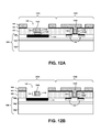
- FIGS. 12A and 12B schematically illustrate a method to release cantilever structures of electromechanical devices in the electromechanical device region of the substrate, according to an embodiment of the disclosure, wherein:
- FIG. 12A is a schematic cross-sectional side view of the semiconductor structure of FIG. 11 after patterning the one or more layers of metallic material to form local interconnect structures between devices in the CMOS and electromechanical device regions;
- FIG. 12B is a schematic cross-sectional side view of the semiconductor structure of FIG. 12A after removing insulating material through an opening formed in a portion of the patterned layer of metallic material in the electromechanical device region to release the electromechanical devices.
- FIGS. 13A, 13B, 13C, and 13D schematically illustrate a method to release cantilever structures of electromechanical devices in the electromechanical device region of the substrate, according to another embodiment of the disclosure, wherein:
- FIG. 13A is a schematic cross-sectional side view of the semiconductor structure of FIG. 11 after planarizing the semiconductor structure down to the insulating layer to remove the layers of metallic material and dielectric material, and sequentially depositing an insulating layer and a nitride layer on the planarized semiconductor structure;
- FIG. 13B is a schematic cross-sectional side view of the semiconductor structure of FIG. 13A after forming via contacts to the metallic gate electrodes and the source/drain regions of transistor devices in the CMOS device region of the substrate;
- FIG. 13C is a schematic cross-sectional side view of the semiconductor structure of FIG. 13B after forming a vent hole opening in the electromechanical device region of the substrate;
- FIG. 13D is a schematic cross-sectional side view of the semiconductor structure of FIG. 13C after removing insulating material through the vent hole opening to release the cantilever structures of electromechanical devices in the electromechanical device region of the substrate.
- FIGS. 14A, 14B, 14C, 14D, 14E, and 14F schematically illustrate a method to release cantilever structures of electromechanical devices in the electromechanical device region of the substrate, according to yet another embodiment of the disclosure, wherein:
- FIG. 14A is a schematic cross-sectional side view of the semiconductor structure of FIG. 13B after forming a guard ring opening around an electromechanical device structure in the electromechanical device region of the substrate;
- FIG. 14B is a top plan schematic view of the electromechanical device region taken along line 14 B- 14 B in FIG. 14A , showing the guard ring opening formed around the electromechanical device structure;
- FIG. 14C is a schematic cross-sectional side view of the semiconductor structure of FIG. 14A after filling the guard ring opening with an insulating material to form a guard ring around the electromechanical device structure in the electromechanical device region of the substrate;
- FIG. 14D is a schematic cross-sectional side view of the semiconductor structure of FIG. 14C after forming a vent hole opening in the electromechanical device region of the substrate;
- FIG. 14E is a schematic cross-sectional side view of the semiconductor structure of FIG. 14D after removing insulating material through the vent hole opening to release the cantilever structure of an electromechanical device in the electromechanical device region of the substrate;
- FIG. 14F is a schematic cross-sectional side view of the semiconductor structure of FIG. 14E after depositing an insulating layer to seal the vent hole and forming via contacts as part of a first level of a back-end-of-line process.
- FIG. 1 is a schematic cross-sectional side view of a semiconductor structure at an initial stage of fabrication starting with a silicon-on-insulator substrate 100 , according to an embodiment of the disclosure.
- the substrate 100 includes a base substrate layer 102 , an insulating layer 104 (e.g., buried oxide layer) and an active semiconductor layer 106 (or SOI layer 106 ).
- the insulating layer 104 isolates the active semiconductor layer 106 from the base substrate 102 .
- the base substrate 102 may be made from any of several known semiconductor materials such as, for example, silicon, germanium, silicon-germanium alloy, silicon carbide, silicon-germanium carbide alloy, and compound (e.g. III-V and II-VI) semiconductor materials.
- Non-limiting examples of compound semiconductor materials include gallium arsenide, indium arsenide, and indium phosphide.
- the thickness of the base substrate 102 will vary depending on the application. For example, the base substrate 102 may have a thickness in a range of about 0.5 mm to about 1.5 mm.
- the insulating layer 104 may be formed of any dielectric or insulating material which is suitable for the given application.
- the insulating layer 104 may be formed of material such as, for example, oxides, nitrides, oxynitrides of silicon, and combinations thereof.
- the insulating layer 104 may include crystalline or non-crystalline dielectric material.
- the insulating layer 104 has a thickness in a range of about 100 nm to about 500 nm, for example.
- the SOI layer 106 may be made of silicon or other suitable types of semiconductor materials, such as materials used for the base substrate 102 .
- the base substrate 102 and the SOI layer 106 may include either identical or different semiconducting materials with respect to chemical composition, dopant concentration, and crystallographic orientation.
- the SOI layer 106 may be doped with p-type dopants such as boron or doped with n-type dopants such as phosphorus and/or arsenic.
- the SOI layer 106 may have a thickness ranging from about 30 nm to about 100 nm, for example.
- the substrate 100 may include a bulk semiconductor substrate formed of, e.g., silicon, or other types of semiconductor substrate materials that are commonly used in bulk semiconductor fabrication processes.
- the substrate 100 includes one or more electromechanical device regions and one or more CMOS device regions.
- FIG. 1 illustrate a portion of one electromechanical (MEMS/NEMS) device region 100 A, and a portion of one CMOS device region 100 B.
- FIG. 2 is a schematic cross-sectional side view of the semiconductor structure of FIG. 1 after forming a doped well 108 for an electromechanical device in the electromechanical region 100 A of the substrate, according to an embodiment of the disclosure.
- the doped well 108 is formed using an ion implantation process in which dopant ions are accelerated in an electrical field and impacted into the surface of the substrate 100 .
- the energy of the dopant ions, as well as the ion species and the material composition of the substrate surface will determine the depth of penetration of the ions into the substrate surface.
- the doped well 108 is formed in the SOI layer 106 of the substrate 100 .
- the doped well 108 can be an n-well that is formed by ion implanting a n-type dopant species (e.g., phosphorus or arsenic) into the substrate 100 , or a p-well that is formed by ion implanting a p-type dopant species (e.g., boron) into the substrate 100 , using known techniques.
- the process of forming the doped well 108 in the substrate 100 is an optional step that is performed only when the electromechanical device contacts are to be formed in the substrate 100 for the given design.
- electromechanical device contacts can be formed above the cantilever components of the electromechanical devices (e.g., in a BEOL structure).
- FIG. 3 is a schematic cross-sectional side view of the semiconductor structure of FIG. 2 after siliciding the doped well 108 to form an ohmic silicide contact 110 , according to an embodiment of the disclosure.
- a silicidation process is implemented to form high melting point silicide contacts which can withstand thermal temperatures of more than 1000 degrees Celsius.
- the ohmic silicide contact 110 may be a high temperature Co-silicide contact or a high temperature Ti-silicide contact, which are formed using known techniques. Other techniques may be implemented to convert the doped wells 108 to ohmic contacts.
- FIG. 4 is a schematic cross-sectional side view of the semiconductor structure of FIG. 3 after forming an insulating layer 112 over the surface of the substrate 100 , according to an embodiment of the disclosure.
- the insulating layer 112 is formed of an oxide material, such as silicon oxide.
- the insulating layer 112 includes a first portion 112 A formed on the ohmic contact 110 , and a second portion 112 B formed on the remaining surface area of the SOI layer 106 .
- the first portion 112 A of the insulating layer 112 is thicker than the second portion 112 B of the insulating layer 112 .
- the thickness of the first portion 112 A of the insulating layer 112 defines a gap distance between a cantilever component of an electromechanical device and the ohmic contact 110 .
- the first portion 112 A of the insulating layer 112 has a thickness in a range of about 1 nm to about 1000 nm.
- the thickness of the second portion 112 B of the insulating layer 112 defines a thickness of a gate oxide layer for FET devices that are formed in the CMOS device region 100 B.
- the second portion 112 B of the insulating layer 112 has a thickness in a range of about 1 nm to about 100 nm.
- the insulating layer 112 may be formed by blanket depositing a thick layer of insulating material over the device regions 100 A and 100 B, etching away the portion of the insulating material which does not cover the ohmic contacts 110 , and then depositing a second layer of insulating material to form the second portion 112 B of the insulating layer 112 .
- additional insulating material may be deposited on the existing insulating material disposed over the ohmic contact 110 such that the total thickness of the first portion 112 A of the insulating layer 112 is defined by the insulating material deposited during the first and second deposition steps.
- a next step in the exemplary process is to form sacrificial structures for the CMOS and electromechanical devices.
- a layer of sacrificial material is deposited and patterned to form sacrificial (dummy) anchor and cantilever structures for electromechanical devices in the device region 100 A, as well as sacrificial (dummy) gate structures for FET devices in the device region 100 B.
- FIG. 5 is a schematic cross-sectional side view of the semiconductor structure of FIG. 4 after depositing a layer of sacrificial material 114 , according to an embodiment of the disclosure.
- the layer of sacrificial material 114 includes a layer of polysilicon, which can be doped or undoped.
- the layer of sacrificial material 114 can be formed by depositing a blanket layer of sacrificial material using any suitable deposition technique known in the art, including atomic layer deposition (ALD), chemical vapor deposition (CVD), physical vapor deposition (PVD), or molecular beam deposition (MBD), for example.
- ALD atomic layer deposition
- CVD chemical vapor deposition
- PVD physical vapor deposition
- MBD molecular beam deposition
- the layer of sacrificial material 114 is deposited, a CMP (chemical-mechanical planarization) process is performed to planarize the surface of the sacrificial material 114 .
- the resulting planarized layer of sacrificial material 114 has a thickness in a range of about 10 nm to about 5000 nm, for example.
- the layer of sacrificial material 114 is patterned (via a suitable lithographic process and etch process) to form sacrificial structures for the electromechanical devices and CMOS devices in the device regions 100 A and 100 B.
- FIG. 6 is a schematic cross-sectional side view of the semiconductor structure of FIG. 5 after patterning the layer of sacrificial material 114 to form sacrificial structures 114 A and 114 B in the device regions 100 A and 100 B, respectively, and forming sidewall spacers 116 on sidewalls of the sacrificial structures 114 A and 114 B, according to an embodiment of the disclosure. More specifically, FIG. 6 illustrates a stage of fabrication in which a gate structure 118 is formed in the CMOS device region 100 B, and an electromechanical device structure 120 is formed in the electromechanical device region 100 A. As shown in FIG.
- the gate structure 118 includes a sacrificial gate electrode structure 114 B, sidewall spacers 116 formed on the sacrificial gate electrode structure 114 B, and a gate insulating layer 112 B which is formed by patterning the thin insulating layer 112 B.
- the electromechanical device structure 120 includes a sacrificial structure 114 A, sidewalls spacers 116 formed on the sidewalls of the sacrificial structure 114 A, and a sacrificial insulating layer 112 A which is formed by patterning the thick insulating layer 112 A.
- the sacrificial structure 114 A defines an anchor structure 122 and a cantilever structure 124 , which are initially formed by patterning the sacrificial material 114 .
- the anchor structure 122 (and associated portion of the sidewall spacer 116 ) is formed down to the substrate 110 , whereas the cantilever structure 124 (and associated portion of the sidewall spacer 116 ) is formed on top of the sacrificial insulating layer 112 A.
- the sacrificial material forming the anchor structure 122 and cantilever structure 124 is replaced with metallic material as part of a replacement metal gate process.
- the structure shown in FIG. 6 can be fabricated as follows.
- the layer of sacrificial material 114 shown in FIG. 5 can be patterned using a standard photolithographic process, for example, where a layer of photoresist material is deposited on top of the layer of sacrificial material 114 and lithographically patterned (exposed and developed) to form a photoresist mask having a target pattern which defines a pattern of the sacrificial structures 114 A and 114 B to be to be transferred to the layer of sacrificial material 114 .
- An etch process is then performed using the photoresist mask to etch exposed portions of the layer of sacrificial material 114 down to the insulating layer 112 , and thereby form the sacrificial structures 114 A and 114 B.
- the etch process can be performed using a dry etch process such as RIE (reactive ion etching) or other anisotropic etch processes with etching chemistries that are suitable to etch the layer of sacrificial material 114 .
- one or more deposition and etching processes are performed to form the sidewall spacers 116 on the sidewalls of the sacrificial structures 114 A and 114 B, and to pattern the insulating layers 112 A and 112 B to form the insulting structures 112 A and 112 B.
- the sidewall spacers 116 are formed by depositing a conformal layer of dielectric/insulting material (e.g., silicon nitride or other suitable material(s)) using known deposition methods, and then anisotropically etching the conformal layer of dielectric/insulating material to remove portions of the conformal layer on horizontal surfaces of the semiconductor structure to thereby form the sidewalls spacers 116 on vertical surfaces of the sacrificial structures 114 A and 114 B. Another etch process is then preformed to remove exposed portions of the insulating layers 112 A and 112 B to form the patterned insulating structures 112 A and 112 B.
- a conformal layer of dielectric/insulting material e.g., silicon nitride or other suitable material(s)
- etch processes that are used to pattern the sidewall spacers 116 and insulating structures 112 A and 112 B are performed using etch chemistries that are selective to the sacrificial material forming the sacrificial structures 114 A and 114 B so as to prevent such structures from being etched away when forming the sidewall spacers 116 and the insulating structures 112 A and 112 B.
- a next step in the example fabrication process includes forming source and drain regions for CMOS devices in the device region 100 B.
- FIG. 7 is a schematic cross-sectional side view of the semiconductor structure of FIG. 6 after forming source and drain regions 126 adjacent to the gate structure 118 in the device region 100 B of the substrate 100 , according to an embodiment of the disclosure.
- the source/drain regions 126 include doped regions 126 - 1 and ohmic contacts 126 - 2 .
- the doped regions 126 - 1 can be p-type or n-typed doped regions that are formed in the SOI layer 106 using ion implantation techniques.
- the ohmic contacts 126 - 2 can be silicide layers that are formed by siliciding an upper surface region of the doped regions 126 - 1 .
- Techniques for fabricating the source/drain regions 126 are well known to those of ordinary skill in the art.
- FIG. 8 is a schematic cross-sectional side view of the semiconductor structure of FIG. 7 after blanket depositing and planarizing a layer of insulating material 128 to expose the sacrificial structures 114 A and 114 B, according to an embodiment of the disclosure.
- the layer of insulating material 128 may be formed of any suitable material such as, e.g., silicon oxide, silicon nitride, hydrogenated silicon carbon oxide, silicon based low-k dielectrics, porous dielectrics, or organic dielectrics including porous organic dielectrics.
- the layer of insulating material 128 may be deposited using known deposition techniques, such as, for example, ALD, CVD, PECVD, PVD, or spin on deposition techniques.
- the layer of insulating material 128 may be etched/planarized using a CMP process, for example, wherein the surface of the semiconductor structure is planarized down to expose the upper surfaces of the sacrificial structures 114 A and 114 B.
- FIG. 9 is a schematic cross-sectional side view of the semiconductor structure of FIG. 8 after removing the sacrificial structures 114 A and 114 B and depositing a conformal layer of dielectric material 132 , according to an embodiment of the disclosure.
- a selective etch process is performed to remove the sacrificial structures 114 A and 114 B selective to the insulating layer 128 and spacers 116 , so as to avoid etching the insulating layer 128 and spacers 116 .
- the selective etch process may include, for example, an anisotropic etching process such as RIE or plasma etching with an etching chemistry that can selectively remove the sacrificial material (e.g., polysilicon) which forms the sacrificial structures 114 A and 114 B.
- the recessed regions 130 A and 130 B are created in the electromechanical device structure 120 and the gate structure 118 , respectively.
- the replacement metal gate process continues with forming the conformal dielectric layer 132 , which serves as a gate dielectric layer for CMOS devices in the device region 100 B.
- the conformal dielectric layer 132 can be formed of any insulating/dielectric material which is suitable to serve as a gate dielectric layer for the target application.
- the conformal dielectric layer 132 may include, e.g., nitride, oxynitride, or oxide or high-k materials such as SiO 2 , HfO 2 , ZrO 2 , Al 2 O 3 , TiO 2 , La 2 O 3 , SrTiO 3 , LaAlO 3 , and mixtures thereof.
- the conformal dielectric layer 132 has a thickness in a range of about 0.5 nm to about 10 nm, which will vary depending on the target application.
- the conformal dielectric layer 132 is deposited using known methods such as ALD, CVD, PVD, or MBD, for example.
- FIG. 10 is a schematic cross-sectional side view of the semiconductor structure of FIG. 9 after removing a portion of the conformal dielectric layer 132 in the electromechanical device region 100 A, according to an embodiment of the disclosure.
- the conformal dielectric layer 132 can be patterned using a standard photolithographic process, for example, where a layer of photoresist material is deposited on top of the conformal dielectric layer 132 and lithographically patterned (exposed and developed) to form a photoresist mask having a target pattern which defines an opening to expose the portions of the conformal dielectric layer 132 to be removed. An etch process is then performed using the photoresist mask to etch away the exposed portions of the conformal dielectric layer 132 and pattern the dielectric layer 132 such as shown in FIG. 10 .
- the etch process can be performed using any suitable isotropic etch process to etch away the exposed portion of the conformal dielectric layer 132 selective to the insulating layer 128 , spacers 116 and sacrificial insulating structure 112 A.
- the photoresist mask is then removed using known methods.
- FIG. 11 is a schematic cross-sectional side view of the semiconductor structure of FIG. 10 after depositing one or more layers of metallic material to form metallic anchor and metallic cantilever structures of the electromechanical device structures 120 in the device region 100 A, and to form metallic gate electrodes for the gate structures 118 of FETs in the device region 100 B, according to an embodiment of the disclosure.
- a layer of metallic material 134 is deposited to fill the recessed regions 130 A and 130 B with metallic material and form metallic anchor and metallic cantilever structures 134 A for the electromechanical device structure 120 in the device region 100 A, and to form a metallic gate electrode 134 B of the gate structure 118 of an FET in the device region 100 B.
- this process may be implemented by depositing one layer of metallic material which is used to form the metallic components (e.g., anchor point, cantilever, gate electrodes) in the device regions 100 A and 100 B, followed by a CMP process to planarize the metallic layer.
- a blocking mask can be formed to cover the electromechanical device region 100 A, followed by deposition and planarization of metallic material in the CMOS device region 100 B to form the metallic gate electrode 134 B, and then removal of the blocking mask. The process is then repeated by forming a blocking mask to cover the CMOS device region 100 B, followed by deposition and planarization of metallic material in the electromechanical device region 100 A to form the metallic anchor and metallic cantilever structure 134 A.
- the metallic gate electrode 134 B may be formed using multiple layers of metallic material including, for example, an initial deposition of a work function metal on the gate dielectric layer 132 within the recessed region 130 B, followed by the deposition of a metallic gate electrode layer.
- the work function metal may include, for example, Zr, W, Ta, Hf, Ti, Al, Ru, Pa, metal oxides, metal carbides, metal nitrides, transition metal aluminides (e.g. Ti 3 Al, ZrAl), TaC, TiC, TaMgC, or any combination thereof.
- the work function metal layer can be formed using known methods such as ALD, CVD, PVD, or MBD, for example.
- the metallic gate electrode layer may be formed of tungsten, doped polysilicon material, or any metallic or conductive material that is commonly used to make gate electrode structures.
- the metallic anchor and metallic cantilever structures 134 A can be made using one of various types of metallic materials that are commonly utilized to form MEMS or NEMS devices.
- a next step in the illustrative fabrication process is to release the electromechanical devices formed in the device region 100 A.
- a release process involves removing insulating material surrounding the cantilever structures extending from the associated anchor structures so that the cantilever structures are enabled for mechanical movement.
- Alternate embodiments of the disclosure for implementing a release process will now be described in further detail with reference to FIGS. 12A ⁇ 12 B, FIGS. 13A ⁇ 13 D, and FIGS. 14A ⁇ 14 F.
- FIGS. 12A and 12B schematically illustrate a method to release electromechanical device structures in the electromechanical device region 100 A of the substrate, according to an embodiment of the disclosure.
- FIG. 12A is a schematic cross-sectional side view of the semiconductor structure of FIG. 11 after patterning the layer of metallic material 134 to form local interconnect structures between devices in the device regions 100 A and 100 B.
- the layer of metallic material 134 can be patterned using a standard subtractive RIE process.
- the layer of metallic material 134 is patterned to form a vent opening 136 to expose a portion of the insulating layer 128 in the electromechanical device region 100 A which is to be removed so as to physically release the cantilever structure 124 .
- FIG. 12B is a schematic cross-sectional side view of the semiconductor structure of FIG. 12A after removing insulating material through the vent opening 136 to release the cantilever structure 124 of the electromechanical device 120 .
- the cantilever structure 124 of the electromechanical device structure 120 is released by etching away a portion of the insulating layer 128 surrounding the cantilever structure 124 and the underlying sacrificial insulting layer 112 A.
- an etch process to release the cantilever structure 124 is performed by forming an etch mask over the semiconductor structure shown in FIG. 12A which covers the entire surface expect for the vent opening 136 .
- a selective etch process is formed to etch the materials (e.g., silicon oxide) of the insulating layer 128 and the underlying sacrificial insulating structure 112 A selective to the materials forming the ohmic contact 110 , the spacers 116 and the metallic anchor and metallic cantilever structure 134 A.
- a timed etch can be implemented to limit the amount of insulating material that is etched away to physically release the cantilever structure 124 .
- FIGS. 13A ⁇ 13 D schematically illustrate a method to release electromechanical device structures in the electromechanical device region 100 A of the substrate, according to another embodiment of the disclosure.
- initial steps of the release process are shown in FIG. 13A , wherein FIG. 13A is a schematic cross-sectional side view of the semiconductor structure of FIG. 11 after planarizing the semiconductor structure (of FIG. 11 ) to remove the layers of metallic material 134 and dielectric material 132 down to the insulating layer 128 , and sequentially depositing an insulating layer 138 (e.g., silicon oxide) and a nitride layer 140 on the planarized semiconductor structure, according to an embodiment of the disclosure.
- an insulating layer 138 e.g., silicon oxide
- a next step includes forming contacts to the source/drain regions 126 and the gate structures 118 of the FETs in the CMOS device region 100 B.
- FIG. 13B is a schematic cross-sectional side view of the semiconductor structure of FIG. 13A after forming via contacts 142 to the metallic gate electrode 134 B and the source/drain regions 126 in the CMOS device region 100 B of the substrate 100 .
- the via contacts 142 can be fabricated using known techniques and formed with one or more layers of conductive materials. For example, via holes are etched through the nitride layer 140 and insulating layers 138 and 128 down to the source/drain regions 126 and metallic gate electrode 134 B of the gate structure 118 .
- the via holes can be lined with a thin conformal barrier diffusion layer, and then filled with a conductive material such as copper or tungsten, for example.
- FIG. 13C is a schematic cross-sectional side view of the semiconductor structure of FIG. 13B after forming a vent hole opening 144 through the nitride layer 140 into the insulating layer 138 in the electromechanical device region 100 A of the substrate.
- FIG. 13D is a schematic cross-sectional side view of the semiconductor structure of FIG.
- insulating material e.g., portions of the insulating layers 138 and 128 and the underlying sacrificial insulating structure 112 A
- an etch process to release the cantilever structure 124 is performed by using the nitride layer 140 as an etch mask, while performing a selective etch process to etch the materials (e.g., silicon oxide) of the insulating layers 128 / 138 and the underlying sacrificial insulating structure 112 A selective to the nitride layer 140 and the ohmic contact 110 , the spacers 116 and the metallic anchor and metallic cantilever structure 134 A.
- a timed etch can be implemented to limit the amount of insulating material that is etched away to physically release the cantilever structure 124 .
- FIGS. 12A ⁇ 12 B and FIGS. 13A ⁇ 13 D can be readily implemented in certain designs in which the electromechanical devices are separated from other devices by distances that exceed the given design rule spacing for the fabrication process. This allows a timed etch to be utilized to etch the insulating materials surrounding the cantilever structure 124 to achieve proper release, without adversely affecting surrounding device structures.
- other techniques can be implemented to limit the amount of undercutting that occurs during the release etch.
- FIGS. 14A ?? 14 F schematically illustrate another method to release electromechanical device structures in the electromechanical device region of the substrate, according to an embodiment of the disclosure in which a protective guard ring is utilized to limit the lateral extent (undercutting) of the etch process that releases the cantilever structure 124 .
- FIG. 14A is a schematic cross-sectional side view of the semiconductor structure of FIG. 13B after performing an etch process to form a guard ring opening 146 around the electromechanical device structure 120 in the electromechanical device region 100 A of the substrate.
- FIG. 14B is a schematic top plan view of the electromechanical device region 100 A taken along line 14 B- 14 B in FIG. 14A , showing the guard ring opening 146 formed around the electromechanical device structure 120 .
- the guard ring opening 146 can be formed using a process which includes patterning the nitride layer 140 using standard photolithographic techniques to form an etch mask pattern of the guard ring opening 146 in the nitride layer 140 , and then using the patterned nitride layer 140 as an etch mask to perform a selective etch process (e.g., RIE) to etch a recess through the insulating layers 138 and 128 down to the SOI layer 106 , selective to the nitride layer 140 , and thereby form the guard ring opening 146 .
- FIG. 14B shows the guard ring opening 146 being rectangular-shaped, the guard ring opening 146 can be formed with other shapes, depending on the application and device layout.
- FIG. 14C is a schematic cross-sectional side view of the semiconductor structure of FIG. 14A after filling the guard ring opening 146 with an insulating material to form a guard ring 148 which surrounds the electromechanical device structure 120 in the electromechanical device region 100 A of the substrate 100 .
- the guard ring 148 is formed with an insulating material, which is different from the materials forming the insulating layers 128 , 138 and 112 A, so that there is high etch selectivity between the guard ring 148 and the insulating layers 128 , 138 , and 112 A.
- the guard ring 148 can be formed of silicon nitride when the insulating layers 128 , 138 , and 112 A are formed of silicon oxide.
- the guard ring 148 can be formed by depositing a silicon nitride material to fill the guard ring opening 146 , followed by a CMP process to remove the excess silicon nitride material down to the nitride layer 140 .
- FIG. 14D is a schematic cross-sectional side view of the semiconductor structure of FIG. 14C after forming a vent hole opening 150 through the nitride layer 140 and into the insulating layer 138 within an inner region the guard ring 148 in the electromechanical device region 100 A of the substrate 100 .
- FIG. 14E is a schematic cross-sectional side view of the semiconductor structure of FIG. 14D after removing insulating material through the vent hole opening 150 to release the cantilever structure 124 of the electromechanical device 120 in the electromechanical device region 100 A.
- any suitable dry or wet etch process can be implemented to isotropically etch the materials of the insulating layers 128 and 138 and the underlying sacrificial insulating structure 112 A selective to the guard ring 148 , for example, to form a cavity within the confines of the guard ring 148 and release the cantilever structure 124 .
- a wet etch process such as a buffered oxide etch with a suitable etching chemistry including a buffering agent and hydrofluoric acid (HF), can be used to etch the material (e.g.
- the guard ring 148 limits the extent of the undercutting of the insulating layers 128 and 138 during the etch process for releasing the cantilever structure 124 .
- FIG. 14F is a schematic cross-sectional side view of the semiconductor structure of FIG. 14E after depositing an insulating layer 152 to seal the vent hole 150 and forming initial via contacts 154 as part of a back-end-of-line process.
- the insulating layer 152 and via contacts 154 may be considered the initial Ml level in a BEOL structure, wherein the insulating layer 152 (or ILD (inter-level dielectric) layer) is formed using materials and methods that are commonly utilized for BEOL processing.
- the via contacts 154 can be formed by etching via holes in the insulating layer 152 , lining the via holes with a thin barrier diffusion layer, and then filling the via holes with conductive material such as tungsten or copper, for example.
- any standard sequence of subsequent processing steps can be implemented to complete the fabrication of the BEOL structure and form other elements of the target integrated circuit to be fabricated, the details of which are not needed to understand embodiments as discussed herein.
- electromechanical devices e.g., NEMS and/or MEMS devices
- CMOS devices such as FETs
- electromechanical devices are co-fabricated along with CMOS FET devices as part of a standard replacement metal gate process. While the semiconductor process flows shown in the accompanying figures illustrate the formation of planar FET devices, it is to be understood that electromechanical devices can be co-fabricated with FinFET or trigate devices, for example.
- Embodiments of the present disclosure provide various advantages over other co-integration methods.
- the gap distance between a cantilever and the substrate can be strictly controlled based on the thickness of the underlying sacrificial insulating structure 112 A (e.g., oxide layer) as shown in FIGS. 4, 5, 6, and 7 .
- This process enables the formation of very small gaps between the cantilever structure 124 and the contact 110 , which allows for the operation of electromechanical devices with low gate control voltages.
- a replacement metal gate process provides the freedom to utilize metallic material to form the cantilever structures during the replacement metal gate process, whether such metallic material is the same or different from the metallic material utilized to form the metallic gate electrodes for CMOS transistor devices.
- embodiments of the present disclosure provide a simple process flow for a 1-level metal connection structure using a subtractive RIE process (e.g., FIGS. 12A and 12B ).
- the co-integration of electromechanical devices in a FEOL implementation results in the electromechanical devices being surrounded by the replacement gate metallization as well as the BEOL metallization, which provides additional RF shielding for the electromechanical devices and, hence, less interference from outside signals, which is desirable for RF applications.
- the co-integration techniques described herein can be implemented in a wide range of applications including, for example, FPGA (field programmable gate array) applications with low leakage and high density, as well as RF applications.
- CMOS devices can be incorporated within semiconductor processing flows for fabricating other types of semiconductor devices and integrated circuits with various analog and digital circuitry or mixed-signal circuitry.
- integrated circuit dies can be fabricated with various devices such as field-effect transistors, bipolar transistors, metal-oxide-semiconductor transistors, diodes, capacitors, inductors, etc.
- An integrated circuit in accordance with the present disclosure can be employed in applications, hardware, and/or electronic systems.
- Suitable hardware and systems for implementing embodiments of the present disclosure may include, but are not limited to, personal computers, communication networks, electronic commerce systems, portable communications devices (e.g., cell phones), solid-state media storage devices, functional circuitry, etc. Systems and hardware incorporating such integrated circuits are considered part of the illustrative embodiments described herein.
Abstract
Description
Claims (14)
Priority Applications (1)
| Application Number | Priority Date | Filing Date | Title |
|---|---|---|---|
| US14/814,083 US9505611B1 (en) | 2015-07-30 | 2015-07-30 | Integration of electromechanical and CMOS devices in front-end-of-line using replacement metal gate process flow |
Applications Claiming Priority (1)
| Application Number | Priority Date | Filing Date | Title |
|---|---|---|---|
| US14/814,083 US9505611B1 (en) | 2015-07-30 | 2015-07-30 | Integration of electromechanical and CMOS devices in front-end-of-line using replacement metal gate process flow |
Publications (1)
| Publication Number | Publication Date |
|---|---|
| US9505611B1 true US9505611B1 (en) | 2016-11-29 |
Family
ID=57351762
Family Applications (1)
| Application Number | Title | Priority Date | Filing Date |
|---|---|---|---|
| US14/814,083 Expired - Fee Related US9505611B1 (en) | 2015-07-30 | 2015-07-30 | Integration of electromechanical and CMOS devices in front-end-of-line using replacement metal gate process flow |
Country Status (1)
| Country | Link |
|---|---|
| US (1) | US9505611B1 (en) |
Cited By (7)
| Publication number | Priority date | Publication date | Assignee | Title |
|---|---|---|---|---|
| CN109336047A (en) * | 2018-10-08 | 2019-02-15 | 东北大学 | A kind of multilayered structure ion source chip and mass spectral analysis sampling system based on MEMS technology |
| CN109573941A (en) * | 2018-11-15 | 2019-04-05 | 中国科学院半导体研究所 | A kind of method for making in scale of CMOS-MEMS integrated chip |
| US20190148424A1 (en) * | 2017-07-19 | 2019-05-16 | Meridian Innovation Pte Ltd | Thermoelectric-based infrared detector with high cmos integration |
| EP3428592A3 (en) * | 2017-07-12 | 2019-05-22 | Meridian Innovation Pte Ltd | Scalable thermoelectric-based infrared detector |
| US20190164842A1 (en) * | 2017-11-30 | 2019-05-30 | Taiwan Semiconductor Manufacturing Co., Ltd. | Prevention of Contact Bottom Void in Semiconductor Fabrication |
| US10923525B2 (en) | 2017-07-12 | 2021-02-16 | Meridian Innovation Pte Ltd | CMOS cap for MEMS devices |
| US11845653B2 (en) | 2019-04-01 | 2023-12-19 | Meridian Innovation Pte Ltd | Heterogenous integration of complementary metal-oxide-semiconductor and MEMS sensors |
Citations (14)
| Publication number | Priority date | Publication date | Assignee | Title |
|---|---|---|---|---|
| US5638946A (en) * | 1996-01-11 | 1997-06-17 | Northeastern University | Micromechanical switch with insulated switch contact |
| US20030015768A1 (en) | 2001-07-23 | 2003-01-23 | Motorola, Inc. | Structure and method for microelectromechanical system (MEMS) devices integrated with other semiconductor structures |
| CN1595633A (en) | 2004-06-29 | 2005-03-16 | 北京大学 | A method for integrating CMOS circuit and bulk silicon MEMS uniwafer |
| US7075393B2 (en) * | 2002-10-25 | 2006-07-11 | Analog Devices, Inc. | Micromachined relay with inorganic insulation |
| US20100258882A1 (en) | 2009-04-10 | 2010-10-14 | Nxp, B.V. | Front end micro cavity |
| CN101875480A (en) | 2009-03-30 | 2010-11-03 | Nxp股份有限公司 | Front end micro cavity |
| US20110140216A1 (en) | 2009-12-16 | 2011-06-16 | Oakland University | Method of wafer-level fabrication of MEMS devices |
| US8692338B2 (en) | 2009-07-29 | 2014-04-08 | Pixart Imaging Inc. | Micro electronic device having CMOS circuit and MEMS resonator formed on common silicon substrate |
| US20140106552A1 (en) | 2012-10-16 | 2014-04-17 | International Business Machines Corporation | Method Of Fabricating MEMS Transistors On Far Back End Of Line |
| US8704315B2 (en) | 2008-06-26 | 2014-04-22 | Cornell University | CMOS integrated micromechanical resonators and methods for fabricating the same |
| CN103824813A (en) | 2014-03-05 | 2014-05-28 | 陈龙 | Monolithic integrated micro-fluorescence analysis system and manufacturing method thereof |
| US20140225250A1 (en) | 2012-11-13 | 2014-08-14 | Baolab Microsystems Sl | Methods and systems for fabrication of low-profile mems cmos devices |
| US8823007B2 (en) | 2009-10-28 | 2014-09-02 | MCube Inc. | Integrated system on chip using multiple MEMS and CMOS devices |
| US20140264474A1 (en) | 2013-03-14 | 2014-09-18 | Taiwan Semiconductor Manufacturing Company, Ltd. | Stacked semiconductor device and method of forming the same related cases |
-
2015
- 2015-07-30 US US14/814,083 patent/US9505611B1/en not_active Expired - Fee Related
Patent Citations (17)
| Publication number | Priority date | Publication date | Assignee | Title |
|---|---|---|---|---|
| US5638946A (en) * | 1996-01-11 | 1997-06-17 | Northeastern University | Micromechanical switch with insulated switch contact |
| US20030015768A1 (en) | 2001-07-23 | 2003-01-23 | Motorola, Inc. | Structure and method for microelectromechanical system (MEMS) devices integrated with other semiconductor structures |
| US7075393B2 (en) * | 2002-10-25 | 2006-07-11 | Analog Devices, Inc. | Micromachined relay with inorganic insulation |
| CN1595633A (en) | 2004-06-29 | 2005-03-16 | 北京大学 | A method for integrating CMOS circuit and bulk silicon MEMS uniwafer |
| US8704315B2 (en) | 2008-06-26 | 2014-04-22 | Cornell University | CMOS integrated micromechanical resonators and methods for fabricating the same |
| CN101875480A (en) | 2009-03-30 | 2010-11-03 | Nxp股份有限公司 | Front end micro cavity |
| CN101875480B (en) | 2009-03-30 | 2014-09-17 | Nxp股份有限公司 | Front end micro cavity |
| US20100258882A1 (en) | 2009-04-10 | 2010-10-14 | Nxp, B.V. | Front end micro cavity |
| US8692338B2 (en) | 2009-07-29 | 2014-04-08 | Pixart Imaging Inc. | Micro electronic device having CMOS circuit and MEMS resonator formed on common silicon substrate |
| US8823007B2 (en) | 2009-10-28 | 2014-09-02 | MCube Inc. | Integrated system on chip using multiple MEMS and CMOS devices |
| US20110140216A1 (en) | 2009-12-16 | 2011-06-16 | Oakland University | Method of wafer-level fabrication of MEMS devices |
| US20140106552A1 (en) | 2012-10-16 | 2014-04-17 | International Business Machines Corporation | Method Of Fabricating MEMS Transistors On Far Back End Of Line |
| US20140103422A1 (en) | 2012-10-16 | 2014-04-17 | International Business Machines Corporation | Structure for mems transistors on far back end of line |
| US8927312B2 (en) * | 2012-10-16 | 2015-01-06 | International Business Machines Corporation | Method of fabricating MEMS transistors on far back end of line |
| US20140225250A1 (en) | 2012-11-13 | 2014-08-14 | Baolab Microsystems Sl | Methods and systems for fabrication of low-profile mems cmos devices |
| US20140264474A1 (en) | 2013-03-14 | 2014-09-18 | Taiwan Semiconductor Manufacturing Company, Ltd. | Stacked semiconductor device and method of forming the same related cases |
| CN103824813A (en) | 2014-03-05 | 2014-05-28 | 陈龙 | Monolithic integrated micro-fluorescence analysis system and manufacturing method thereof |
Non-Patent Citations (2)
| Title |
|---|
| English translation for Chinese Application No. CN101875480B. |
| English translation for Chinese Application No. CN1595633A. |
Cited By (14)
| Publication number | Priority date | Publication date | Assignee | Title |
|---|---|---|---|---|
| US10903262B2 (en) | 2017-07-12 | 2021-01-26 | Meridian Innovation Pte Ltd | Scalable thermoelectric-based infrared detector |
| US11848348B2 (en) | 2017-07-12 | 2023-12-19 | Meridian Innovation Pte Ltd | Scalable thermoelectric-based infrared detector |
| US20210159263A1 (en) * | 2017-07-12 | 2021-05-27 | Meridian Innovation Pte Ltd | Cmos cap for mems devices |
| EP3428592A3 (en) * | 2017-07-12 | 2019-05-22 | Meridian Innovation Pte Ltd | Scalable thermoelectric-based infrared detector |
| US10923525B2 (en) | 2017-07-12 | 2021-02-16 | Meridian Innovation Pte Ltd | CMOS cap for MEMS devices |
| US10403674B2 (en) | 2017-07-12 | 2019-09-03 | Meridian Innovation Pte Ltd | Scalable thermoelectric-based infrared detector |
| US10937824B2 (en) * | 2017-07-19 | 2021-03-02 | Meridian Innovation Pte Ltd | Method for manufacturing a thermoelectric-based infrared detector having a MEMS structure above a hybrid component |
| US20190148424A1 (en) * | 2017-07-19 | 2019-05-16 | Meridian Innovation Pte Ltd | Thermoelectric-based infrared detector with high cmos integration |
| US10825737B2 (en) * | 2017-11-30 | 2020-11-03 | Taiwan Semiconductor Manufacturing Co., Ltd. | Prevention of contact bottom void in semiconductor fabrication |
| US20190164842A1 (en) * | 2017-11-30 | 2019-05-30 | Taiwan Semiconductor Manufacturing Co., Ltd. | Prevention of Contact Bottom Void in Semiconductor Fabrication |
| US11362003B2 (en) | 2017-11-30 | 2022-06-14 | Taiwan Semiconductor Manufacturing Co., Ltd. | Prevention of contact bottom void in semiconductor fabrication |
| CN109336047A (en) * | 2018-10-08 | 2019-02-15 | 东北大学 | A kind of multilayered structure ion source chip and mass spectral analysis sampling system based on MEMS technology |
| CN109573941A (en) * | 2018-11-15 | 2019-04-05 | 中国科学院半导体研究所 | A kind of method for making in scale of CMOS-MEMS integrated chip |
| US11845653B2 (en) | 2019-04-01 | 2023-12-19 | Meridian Innovation Pte Ltd | Heterogenous integration of complementary metal-oxide-semiconductor and MEMS sensors |
Similar Documents
| Publication | Publication Date | Title |
|---|---|---|
| US9505611B1 (en) | Integration of electromechanical and CMOS devices in front-end-of-line using replacement metal gate process flow | |
| US9548385B1 (en) | Self-aligned contacts for vertical field effect transistors | |
| US9947766B2 (en) | Semiconductor device and fabricating method thereof | |
| US9431296B2 (en) | Structure and method to form liner silicide with improved contact resistance and reliablity | |
| US20200075476A1 (en) | Semiconductor Device including a Conductive Feature Over an Active Region | |
| US10847513B2 (en) | Buried interconnect conductor | |
| CN103165674B (en) | There is the FinFET of multi-Vt | |
| US9196694B2 (en) | Integrated circuits with dual silicide contacts and methods for fabricating same | |
| US9735251B2 (en) | Semiconductor structure and fabrication method thereof | |
| KR20160065057A (en) | Finfet with buried insulator layer and method for forming | |
| US8969922B2 (en) | Field effect transistors and method of forming the same | |
| US10446435B2 (en) | Local trap-rich isolation | |
| US9425048B2 (en) | Mechanisms for semiconductor device structure | |
| CN103066021A (en) | Semiconductor device having metal gate electrode and method of fabrication thereof | |
| US11271103B2 (en) | Semiconductor device and manufacturing process thereof | |
| TWI783502B (en) | Semiconductor structure and method of formation | |
| US9893145B1 (en) | On chip MIM capacitor | |
| CN110911493A (en) | Integrated circuit device and forming method thereof | |
| US20220037212A1 (en) | Scalable Device for FINFET Technology | |
| CN103094217B (en) | Manufacture method of transistor | |
| US8021986B2 (en) | Method for producing a transistor with metallic source and drain | |
| CN108022975B (en) | Semiconductor device, manufacturing method thereof and electronic device | |
| TW201926704A (en) | Semiconductor device | |
| US20230086633A1 (en) | Semiconductor structure having bottom isolation and enhanced carrier mobility |
Legal Events
| Date | Code | Title | Description |
|---|---|---|---|
| AS | Assignment |
Owner name: GLOBALFOUNDRIES INC., CAYMAN ISLANDS Free format text: ASSIGNMENT OF ASSIGNORS INTEREST;ASSIGNORS:LIU, FEI;OUYANG, QIQING C.;WONG, KEITH KWONG HON;SIGNING DATES FROM 20150724 TO 20150725;REEL/FRAME:036220/0688 |
|
| FEPP | Fee payment procedure |
Free format text: PAYOR NUMBER ASSIGNED (ORIGINAL EVENT CODE: ASPN); ENTITY STATUS OF PATENT OWNER: LARGE ENTITY Free format text: PAYER NUMBER DE-ASSIGNED (ORIGINAL EVENT CODE: RMPN); ENTITY STATUS OF PATENT OWNER: LARGE ENTITY |
|
| STCF | Information on status: patent grant |
Free format text: PATENTED CASE |
|
| AS | Assignment |
Owner name: WILMINGTON TRUST, NATIONAL ASSOCIATION, DELAWARE Free format text: SECURITY AGREEMENT;ASSIGNOR:GLOBALFOUNDRIES INC.;REEL/FRAME:049490/0001 Effective date: 20181127 |
|
| FEPP | Fee payment procedure |
Free format text: MAINTENANCE FEE REMINDER MAILED (ORIGINAL EVENT CODE: REM.); ENTITY STATUS OF PATENT OWNER: LARGE ENTITY |
|
| AS | Assignment |
Owner name: GLOBALFOUNDRIES INC., CAYMAN ISLANDS Free format text: RELEASE BY SECURED PARTY;ASSIGNOR:WILMINGTON TRUST, NATIONAL ASSOCIATION;REEL/FRAME:054636/0001 Effective date: 20201117 |
|
| LAPS | Lapse for failure to pay maintenance fees |
Free format text: PATENT EXPIRED FOR FAILURE TO PAY MAINTENANCE FEES (ORIGINAL EVENT CODE: EXP.); ENTITY STATUS OF PATENT OWNER: LARGE ENTITY |
|
| STCH | Information on status: patent discontinuation |
Free format text: PATENT EXPIRED DUE TO NONPAYMENT OF MAINTENANCE FEES UNDER 37 CFR 1.362 |
|
| FP | Lapsed due to failure to pay maintenance fee |
Effective date: 20201129 |
|
| AS | Assignment |
Owner name: GLOBALFOUNDRIES U.S. INC., NEW YORK Free format text: RELEASE BY SECURED PARTY;ASSIGNOR:WILMINGTON TRUST, NATIONAL ASSOCIATION;REEL/FRAME:056987/0001 Effective date: 20201117 |