US9496154B2 - Use of underfill tape in microelectronic components, and microelectronic components with cavities coupled to through-substrate vias - Google Patents
Use of underfill tape in microelectronic components, and microelectronic components with cavities coupled to through-substrate vias Download PDFInfo
- Publication number
- US9496154B2 US9496154B2 US14/488,187 US201414488187A US9496154B2 US 9496154 B2 US9496154 B2 US 9496154B2 US 201414488187 A US201414488187 A US 201414488187A US 9496154 B2 US9496154 B2 US 9496154B2
- Authority
- US
- United States
- Prior art keywords
- cavity
- contact pad
- microelectronic component
- component
- tape
- Prior art date
- Legal status (The legal status is an assumption and is not a legal conclusion. Google has not performed a legal analysis and makes no representation as to the accuracy of the status listed.)
- Active
Links
- 238000004377 microelectronic Methods 0.000 title claims abstract description 58
- 239000000758 substrate Substances 0.000 title claims abstract description 48
- 239000011800 void material Substances 0.000 claims abstract description 24
- 238000000034 method Methods 0.000 claims description 35
- 239000000463 material Substances 0.000 claims description 14
- 239000004020 conductor Substances 0.000 claims description 11
- 238000004519 manufacturing process Methods 0.000 claims description 8
- 239000007788 liquid Substances 0.000 claims description 5
- 229910000679 solder Inorganic materials 0.000 description 27
- 239000000853 adhesive Substances 0.000 description 20
- 230000001070 adhesive effect Effects 0.000 description 20
- 235000012431 wafers Nutrition 0.000 description 10
- 238000005516 engineering process Methods 0.000 description 4
- 239000007787 solid Substances 0.000 description 4
- RYGMFSIKBFXOCR-UHFFFAOYSA-N Copper Chemical compound [Cu] RYGMFSIKBFXOCR-UHFFFAOYSA-N 0.000 description 3
- 229910052802 copper Inorganic materials 0.000 description 3
- 239000010949 copper Substances 0.000 description 3
- 229920000642 polymer Polymers 0.000 description 3
- VYPSYNLAJGMNEJ-UHFFFAOYSA-N Silicium dioxide Chemical compound O=[Si]=O VYPSYNLAJGMNEJ-UHFFFAOYSA-N 0.000 description 2
- 230000004888 barrier function Effects 0.000 description 2
- UMIVXZPTRXBADB-UHFFFAOYSA-N benzocyclobutene Chemical compound C1=CC=C2CCC2=C1 UMIVXZPTRXBADB-UHFFFAOYSA-N 0.000 description 2
- 239000007767 bonding agent Substances 0.000 description 2
- 239000000945 filler Substances 0.000 description 2
- 239000000203 mixture Substances 0.000 description 2
- 229920000620 organic polymer Polymers 0.000 description 2
- 238000000059 patterning Methods 0.000 description 2
- 230000035515 penetration Effects 0.000 description 2
- 238000000206 photolithography Methods 0.000 description 2
- 229920002120 photoresistant polymer Polymers 0.000 description 2
- 239000004593 Epoxy Substances 0.000 description 1
- 239000004642 Polyimide Substances 0.000 description 1
- 229910000831 Steel Inorganic materials 0.000 description 1
- 238000010420 art technique Methods 0.000 description 1
- 239000003990 capacitor Substances 0.000 description 1
- 230000008602 contraction Effects 0.000 description 1
- 230000008021 deposition Effects 0.000 description 1
- 239000004205 dimethyl polysiloxane Substances 0.000 description 1
- 235000013870 dimethyl polysiloxane Nutrition 0.000 description 1
- 238000009713 electroplating Methods 0.000 description 1
- 230000006870 function Effects 0.000 description 1
- 239000011521 glass Substances 0.000 description 1
- 239000003292 glue Substances 0.000 description 1
- CXQXSVUQTKDNFP-UHFFFAOYSA-N octamethyltrisiloxane Chemical compound C[Si](C)(C)O[Si](C)(C)O[Si](C)(C)C CXQXSVUQTKDNFP-UHFFFAOYSA-N 0.000 description 1
- 230000003071 parasitic effect Effects 0.000 description 1
- 238000004987 plasma desorption mass spectroscopy Methods 0.000 description 1
- 229920000435 poly(dimethylsiloxane) Polymers 0.000 description 1
- 229920001721 polyimide Polymers 0.000 description 1
- 239000004065 semiconductor Substances 0.000 description 1
- 238000007493 shaping process Methods 0.000 description 1
- 229910052710 silicon Inorganic materials 0.000 description 1
- 239000010703 silicon Substances 0.000 description 1
- 239000000377 silicon dioxide Substances 0.000 description 1
- 239000010959 steel Substances 0.000 description 1
Images


Classifications
-
- H—ELECTRICITY
- H01—ELECTRIC ELEMENTS
- H01L—SEMICONDUCTOR DEVICES NOT COVERED BY CLASS H10
- H01L21/00—Processes or apparatus adapted for the manufacture or treatment of semiconductor or solid state devices or of parts thereof
- H01L21/02—Manufacture or treatment of semiconductor devices or of parts thereof
- H01L21/04—Manufacture or treatment of semiconductor devices or of parts thereof the devices having at least one potential-jump barrier or surface barrier, e.g. PN junction, depletion layer or carrier concentration layer
- H01L21/50—Assembly of semiconductor devices using processes or apparatus not provided for in a single one of the subgroups H01L21/06 - H01L21/326, e.g. sealing of a cap to a base of a container
- H01L21/56—Encapsulations, e.g. encapsulation layers, coatings
- H01L21/563—Encapsulation of active face of flip-chip device, e.g. underfilling or underencapsulation of flip-chip, encapsulation preform on chip or mounting substrate
-
- H—ELECTRICITY
- H01—ELECTRIC ELEMENTS
- H01L—SEMICONDUCTOR DEVICES NOT COVERED BY CLASS H10
- H01L23/00—Details of semiconductor or other solid state devices
- H01L23/28—Encapsulations, e.g. encapsulating layers, coatings, e.g. for protection
- H01L23/31—Encapsulations, e.g. encapsulating layers, coatings, e.g. for protection characterised by the arrangement or shape
- H01L23/3157—Partial encapsulation or coating
- H01L23/3178—Coating or filling in grooves made in the semiconductor body
-
- H—ELECTRICITY
- H01—ELECTRIC ELEMENTS
- H01L—SEMICONDUCTOR DEVICES NOT COVERED BY CLASS H10
- H01L24/00—Arrangements for connecting or disconnecting semiconductor or solid-state bodies; Methods or apparatus related thereto
- H01L24/01—Means for bonding being attached to, or being formed on, the surface to be connected, e.g. chip-to-package, die-attach, "first-level" interconnects; Manufacturing methods related thereto
- H01L24/02—Bonding areas ; Manufacturing methods related thereto
- H01L24/04—Structure, shape, material or disposition of the bonding areas prior to the connecting process
- H01L24/06—Structure, shape, material or disposition of the bonding areas prior to the connecting process of a plurality of bonding areas
-
- H—ELECTRICITY
- H01—ELECTRIC ELEMENTS
- H01L—SEMICONDUCTOR DEVICES NOT COVERED BY CLASS H10
- H01L24/00—Arrangements for connecting or disconnecting semiconductor or solid-state bodies; Methods or apparatus related thereto
- H01L24/01—Means for bonding being attached to, or being formed on, the surface to be connected, e.g. chip-to-package, die-attach, "first-level" interconnects; Manufacturing methods related thereto
- H01L24/10—Bump connectors ; Manufacturing methods related thereto
- H01L24/15—Structure, shape, material or disposition of the bump connectors after the connecting process
- H01L24/16—Structure, shape, material or disposition of the bump connectors after the connecting process of an individual bump connector
-
- H—ELECTRICITY
- H01—ELECTRIC ELEMENTS
- H01L—SEMICONDUCTOR DEVICES NOT COVERED BY CLASS H10
- H01L24/00—Arrangements for connecting or disconnecting semiconductor or solid-state bodies; Methods or apparatus related thereto
- H01L24/80—Methods for connecting semiconductor or other solid state bodies using means for bonding being attached to, or being formed on, the surface to be connected
- H01L24/81—Methods for connecting semiconductor or other solid state bodies using means for bonding being attached to, or being formed on, the surface to be connected using a bump connector
-
- H—ELECTRICITY
- H01—ELECTRIC ELEMENTS
- H01L—SEMICONDUCTOR DEVICES NOT COVERED BY CLASS H10
- H01L24/00—Arrangements for connecting or disconnecting semiconductor or solid-state bodies; Methods or apparatus related thereto
- H01L24/80—Methods for connecting semiconductor or other solid state bodies using means for bonding being attached to, or being formed on, the surface to be connected
- H01L24/83—Methods for connecting semiconductor or other solid state bodies using means for bonding being attached to, or being formed on, the surface to be connected using a layer connector
-
- H—ELECTRICITY
- H01—ELECTRIC ELEMENTS
- H01L—SEMICONDUCTOR DEVICES NOT COVERED BY CLASS H10
- H01L24/00—Arrangements for connecting or disconnecting semiconductor or solid-state bodies; Methods or apparatus related thereto
- H01L24/91—Methods for connecting semiconductor or solid state bodies including different methods provided for in two or more of groups H01L24/80 - H01L24/90
-
- H—ELECTRICITY
- H01—ELECTRIC ELEMENTS
- H01L—SEMICONDUCTOR DEVICES NOT COVERED BY CLASS H10
- H01L25/00—Assemblies consisting of a plurality of individual semiconductor or other solid state devices ; Multistep manufacturing processes thereof
- H01L25/03—Assemblies consisting of a plurality of individual semiconductor or other solid state devices ; Multistep manufacturing processes thereof all the devices being of a type provided for in the same subgroup of groups H01L27/00 - H01L33/00, or in a single subclass of H10K, H10N, e.g. assemblies of rectifier diodes
- H01L25/04—Assemblies consisting of a plurality of individual semiconductor or other solid state devices ; Multistep manufacturing processes thereof all the devices being of a type provided for in the same subgroup of groups H01L27/00 - H01L33/00, or in a single subclass of H10K, H10N, e.g. assemblies of rectifier diodes the devices not having separate containers
- H01L25/065—Assemblies consisting of a plurality of individual semiconductor or other solid state devices ; Multistep manufacturing processes thereof all the devices being of a type provided for in the same subgroup of groups H01L27/00 - H01L33/00, or in a single subclass of H10K, H10N, e.g. assemblies of rectifier diodes the devices not having separate containers the devices being of a type provided for in group H01L27/00
- H01L25/0657—Stacked arrangements of devices
-
- H—ELECTRICITY
- H01—ELECTRIC ELEMENTS
- H01L—SEMICONDUCTOR DEVICES NOT COVERED BY CLASS H10
- H01L25/00—Assemblies consisting of a plurality of individual semiconductor or other solid state devices ; Multistep manufacturing processes thereof
- H01L25/50—Multistep manufacturing processes of assemblies consisting of devices, each device being of a type provided for in group H01L27/00 or H01L29/00
-
- H—ELECTRICITY
- H01—ELECTRIC ELEMENTS
- H01L—SEMICONDUCTOR DEVICES NOT COVERED BY CLASS H10
- H01L21/00—Processes or apparatus adapted for the manufacture or treatment of semiconductor or solid state devices or of parts thereof
- H01L21/02—Manufacture or treatment of semiconductor devices or of parts thereof
- H01L21/04—Manufacture or treatment of semiconductor devices or of parts thereof the devices having at least one potential-jump barrier or surface barrier, e.g. PN junction, depletion layer or carrier concentration layer
- H01L21/48—Manufacture or treatment of parts, e.g. containers, prior to assembly of the devices, using processes not provided for in a single one of the subgroups H01L21/06 - H01L21/326
- H01L21/4803—Insulating or insulated parts, e.g. mountings, containers, diamond heatsinks
- H01L21/481—Insulating layers on insulating parts, with or without metallisation
-
- H—ELECTRICITY
- H01—ELECTRIC ELEMENTS
- H01L—SEMICONDUCTOR DEVICES NOT COVERED BY CLASS H10
- H01L2224/00—Indexing scheme for arrangements for connecting or disconnecting semiconductor or solid-state bodies and methods related thereto as covered by H01L24/00
- H01L2224/01—Means for bonding being attached to, or being formed on, the surface to be connected, e.g. chip-to-package, die-attach, "first-level" interconnects; Manufacturing methods related thereto
- H01L2224/02—Bonding areas; Manufacturing methods related thereto
- H01L2224/04—Structure, shape, material or disposition of the bonding areas prior to the connecting process
- H01L2224/05—Structure, shape, material or disposition of the bonding areas prior to the connecting process of an individual bonding area
- H01L2224/0554—External layer
- H01L2224/0556—Disposition
- H01L2224/05568—Disposition the whole external layer protruding from the surface
-
- H—ELECTRICITY
- H01—ELECTRIC ELEMENTS
- H01L—SEMICONDUCTOR DEVICES NOT COVERED BY CLASS H10
- H01L2224/00—Indexing scheme for arrangements for connecting or disconnecting semiconductor or solid-state bodies and methods related thereto as covered by H01L24/00
- H01L2224/01—Means for bonding being attached to, or being formed on, the surface to be connected, e.g. chip-to-package, die-attach, "first-level" interconnects; Manufacturing methods related thereto
- H01L2224/02—Bonding areas; Manufacturing methods related thereto
- H01L2224/04—Structure, shape, material or disposition of the bonding areas prior to the connecting process
- H01L2224/05—Structure, shape, material or disposition of the bonding areas prior to the connecting process of an individual bonding area
- H01L2224/0554—External layer
- H01L2224/0556—Disposition
- H01L2224/05571—Disposition the external layer being disposed in a recess of the surface
-
- H—ELECTRICITY
- H01—ELECTRIC ELEMENTS
- H01L—SEMICONDUCTOR DEVICES NOT COVERED BY CLASS H10
- H01L2224/00—Indexing scheme for arrangements for connecting or disconnecting semiconductor or solid-state bodies and methods related thereto as covered by H01L24/00
- H01L2224/01—Means for bonding being attached to, or being formed on, the surface to be connected, e.g. chip-to-package, die-attach, "first-level" interconnects; Manufacturing methods related thereto
- H01L2224/02—Bonding areas; Manufacturing methods related thereto
- H01L2224/04—Structure, shape, material or disposition of the bonding areas prior to the connecting process
- H01L2224/06—Structure, shape, material or disposition of the bonding areas prior to the connecting process of a plurality of bonding areas
- H01L2224/061—Disposition
- H01L2224/06102—Disposition the bonding areas being at different heights
-
- H—ELECTRICITY
- H01—ELECTRIC ELEMENTS
- H01L—SEMICONDUCTOR DEVICES NOT COVERED BY CLASS H10
- H01L2224/00—Indexing scheme for arrangements for connecting or disconnecting semiconductor or solid-state bodies and methods related thereto as covered by H01L24/00
- H01L2224/01—Means for bonding being attached to, or being formed on, the surface to be connected, e.g. chip-to-package, die-attach, "first-level" interconnects; Manufacturing methods related thereto
- H01L2224/10—Bump connectors; Manufacturing methods related thereto
- H01L2224/12—Structure, shape, material or disposition of the bump connectors prior to the connecting process
- H01L2224/13—Structure, shape, material or disposition of the bump connectors prior to the connecting process of an individual bump connector
- H01L2224/13001—Core members of the bump connector
- H01L2224/1302—Disposition
- H01L2224/13022—Disposition the bump connector being at least partially embedded in the surface
-
- H—ELECTRICITY
- H01—ELECTRIC ELEMENTS
- H01L—SEMICONDUCTOR DEVICES NOT COVERED BY CLASS H10
- H01L2224/00—Indexing scheme for arrangements for connecting or disconnecting semiconductor or solid-state bodies and methods related thereto as covered by H01L24/00
- H01L2224/01—Means for bonding being attached to, or being formed on, the surface to be connected, e.g. chip-to-package, die-attach, "first-level" interconnects; Manufacturing methods related thereto
- H01L2224/10—Bump connectors; Manufacturing methods related thereto
- H01L2224/12—Structure, shape, material or disposition of the bump connectors prior to the connecting process
- H01L2224/13—Structure, shape, material or disposition of the bump connectors prior to the connecting process of an individual bump connector
- H01L2224/13001—Core members of the bump connector
- H01L2224/1302—Disposition
- H01L2224/13023—Disposition the whole bump connector protruding from the surface
-
- H—ELECTRICITY
- H01—ELECTRIC ELEMENTS
- H01L—SEMICONDUCTOR DEVICES NOT COVERED BY CLASS H10
- H01L2224/00—Indexing scheme for arrangements for connecting or disconnecting semiconductor or solid-state bodies and methods related thereto as covered by H01L24/00
- H01L2224/01—Means for bonding being attached to, or being formed on, the surface to be connected, e.g. chip-to-package, die-attach, "first-level" interconnects; Manufacturing methods related thereto
- H01L2224/10—Bump connectors; Manufacturing methods related thereto
- H01L2224/15—Structure, shape, material or disposition of the bump connectors after the connecting process
- H01L2224/16—Structure, shape, material or disposition of the bump connectors after the connecting process of an individual bump connector
- H01L2224/161—Disposition
- H01L2224/16151—Disposition the bump connector connecting between a semiconductor or solid-state body and an item not being a semiconductor or solid-state body, e.g. chip-to-substrate, chip-to-passive
- H01L2224/16221—Disposition the bump connector connecting between a semiconductor or solid-state body and an item not being a semiconductor or solid-state body, e.g. chip-to-substrate, chip-to-passive the body and the item being stacked
- H01L2224/16225—Disposition the bump connector connecting between a semiconductor or solid-state body and an item not being a semiconductor or solid-state body, e.g. chip-to-substrate, chip-to-passive the body and the item being stacked the item being non-metallic, e.g. insulating substrate with or without metallisation
- H01L2224/16237—Disposition the bump connector connecting between a semiconductor or solid-state body and an item not being a semiconductor or solid-state body, e.g. chip-to-substrate, chip-to-passive the body and the item being stacked the item being non-metallic, e.g. insulating substrate with or without metallisation the bump connector connecting to a bonding area disposed in a recess of the surface of the item
-
- H—ELECTRICITY
- H01—ELECTRIC ELEMENTS
- H01L—SEMICONDUCTOR DEVICES NOT COVERED BY CLASS H10
- H01L2224/00—Indexing scheme for arrangements for connecting or disconnecting semiconductor or solid-state bodies and methods related thereto as covered by H01L24/00
- H01L2224/01—Means for bonding being attached to, or being formed on, the surface to be connected, e.g. chip-to-package, die-attach, "first-level" interconnects; Manufacturing methods related thereto
- H01L2224/26—Layer connectors, e.g. plate connectors, solder or adhesive layers; Manufacturing methods related thereto
- H01L2224/28—Structure, shape, material or disposition of the layer connectors prior to the connecting process
- H01L2224/29—Structure, shape, material or disposition of the layer connectors prior to the connecting process of an individual layer connector
- H01L2224/29001—Core members of the layer connector
- H01L2224/29075—Plural core members
- H01L2224/2908—Plural core members being stacked
-
- H—ELECTRICITY
- H01—ELECTRIC ELEMENTS
- H01L—SEMICONDUCTOR DEVICES NOT COVERED BY CLASS H10
- H01L2224/00—Indexing scheme for arrangements for connecting or disconnecting semiconductor or solid-state bodies and methods related thereto as covered by H01L24/00
- H01L2224/01—Means for bonding being attached to, or being formed on, the surface to be connected, e.g. chip-to-package, die-attach, "first-level" interconnects; Manufacturing methods related thereto
- H01L2224/26—Layer connectors, e.g. plate connectors, solder or adhesive layers; Manufacturing methods related thereto
- H01L2224/28—Structure, shape, material or disposition of the layer connectors prior to the connecting process
- H01L2224/29—Structure, shape, material or disposition of the layer connectors prior to the connecting process of an individual layer connector
- H01L2224/29001—Core members of the layer connector
- H01L2224/29099—Material
- H01L2224/2919—Material with a principal constituent of the material being a polymer, e.g. polyester, phenolic based polymer, epoxy
-
- H—ELECTRICITY
- H01—ELECTRIC ELEMENTS
- H01L—SEMICONDUCTOR DEVICES NOT COVERED BY CLASS H10
- H01L2224/00—Indexing scheme for arrangements for connecting or disconnecting semiconductor or solid-state bodies and methods related thereto as covered by H01L24/00
- H01L2224/01—Means for bonding being attached to, or being formed on, the surface to be connected, e.g. chip-to-package, die-attach, "first-level" interconnects; Manufacturing methods related thereto
- H01L2224/26—Layer connectors, e.g. plate connectors, solder or adhesive layers; Manufacturing methods related thereto
- H01L2224/28—Structure, shape, material or disposition of the layer connectors prior to the connecting process
- H01L2224/29—Structure, shape, material or disposition of the layer connectors prior to the connecting process of an individual layer connector
- H01L2224/29001—Core members of the layer connector
- H01L2224/29099—Material
- H01L2224/29198—Material with a principal constituent of the material being a combination of two or more materials in the form of a matrix with a filler, i.e. being a hybrid material, e.g. segmented structures, foams
- H01L2224/29199—Material of the matrix
- H01L2224/2929—Material of the matrix with a principal constituent of the material being a polymer, e.g. polyester, phenolic based polymer, epoxy
-
- H—ELECTRICITY
- H01—ELECTRIC ELEMENTS
- H01L—SEMICONDUCTOR DEVICES NOT COVERED BY CLASS H10
- H01L2224/00—Indexing scheme for arrangements for connecting or disconnecting semiconductor or solid-state bodies and methods related thereto as covered by H01L24/00
- H01L2224/01—Means for bonding being attached to, or being formed on, the surface to be connected, e.g. chip-to-package, die-attach, "first-level" interconnects; Manufacturing methods related thereto
- H01L2224/26—Layer connectors, e.g. plate connectors, solder or adhesive layers; Manufacturing methods related thereto
- H01L2224/28—Structure, shape, material or disposition of the layer connectors prior to the connecting process
- H01L2224/29—Structure, shape, material or disposition of the layer connectors prior to the connecting process of an individual layer connector
- H01L2224/29001—Core members of the layer connector
- H01L2224/29099—Material
- H01L2224/29198—Material with a principal constituent of the material being a combination of two or more materials in the form of a matrix with a filler, i.e. being a hybrid material, e.g. segmented structures, foams
- H01L2224/29298—Fillers
- H01L2224/29299—Base material
- H01L2224/29386—Base material with a principal constituent of the material being a non metallic, non metalloid inorganic material
- H01L2224/29388—Glasses, e.g. amorphous oxides, nitrides or fluorides
-
- H—ELECTRICITY
- H01—ELECTRIC ELEMENTS
- H01L—SEMICONDUCTOR DEVICES NOT COVERED BY CLASS H10
- H01L2224/00—Indexing scheme for arrangements for connecting or disconnecting semiconductor or solid-state bodies and methods related thereto as covered by H01L24/00
- H01L2224/73—Means for bonding being of different types provided for in two or more of groups H01L2224/10, H01L2224/18, H01L2224/26, H01L2224/34, H01L2224/42, H01L2224/50, H01L2224/63, H01L2224/71
- H01L2224/731—Location prior to the connecting process
- H01L2224/73101—Location prior to the connecting process on the same surface
- H01L2224/73103—Bump and layer connectors
- H01L2224/73104—Bump and layer connectors the bump connector being embedded into the layer connector
-
- H—ELECTRICITY
- H01—ELECTRIC ELEMENTS
- H01L—SEMICONDUCTOR DEVICES NOT COVERED BY CLASS H10
- H01L2224/00—Indexing scheme for arrangements for connecting or disconnecting semiconductor or solid-state bodies and methods related thereto as covered by H01L24/00
- H01L2224/73—Means for bonding being of different types provided for in two or more of groups H01L2224/10, H01L2224/18, H01L2224/26, H01L2224/34, H01L2224/42, H01L2224/50, H01L2224/63, H01L2224/71
- H01L2224/732—Location after the connecting process
- H01L2224/73201—Location after the connecting process on the same surface
- H01L2224/73203—Bump and layer connectors
- H01L2224/73204—Bump and layer connectors the bump connector being embedded into the layer connector
-
- H—ELECTRICITY
- H01—ELECTRIC ELEMENTS
- H01L—SEMICONDUCTOR DEVICES NOT COVERED BY CLASS H10
- H01L2224/00—Indexing scheme for arrangements for connecting or disconnecting semiconductor or solid-state bodies and methods related thereto as covered by H01L24/00
- H01L2224/80—Methods for connecting semiconductor or other solid state bodies using means for bonding being attached to, or being formed on, the surface to be connected
- H01L2224/81—Methods for connecting semiconductor or other solid state bodies using means for bonding being attached to, or being formed on, the surface to be connected using a bump connector
- H01L2224/8119—Arrangement of the bump connectors prior to mounting
- H01L2224/81191—Arrangement of the bump connectors prior to mounting wherein the bump connectors are disposed only on the semiconductor or solid-state body
-
- H—ELECTRICITY
- H01—ELECTRIC ELEMENTS
- H01L—SEMICONDUCTOR DEVICES NOT COVERED BY CLASS H10
- H01L2224/00—Indexing scheme for arrangements for connecting or disconnecting semiconductor or solid-state bodies and methods related thereto as covered by H01L24/00
- H01L2224/80—Methods for connecting semiconductor or other solid state bodies using means for bonding being attached to, or being formed on, the surface to be connected
- H01L2224/81—Methods for connecting semiconductor or other solid state bodies using means for bonding being attached to, or being formed on, the surface to be connected using a bump connector
- H01L2224/8119—Arrangement of the bump connectors prior to mounting
- H01L2224/81193—Arrangement of the bump connectors prior to mounting wherein the bump connectors are disposed on both the semiconductor or solid-state body and another item or body to be connected to the semiconductor or solid-state body
-
- H—ELECTRICITY
- H01—ELECTRIC ELEMENTS
- H01L—SEMICONDUCTOR DEVICES NOT COVERED BY CLASS H10
- H01L2224/00—Indexing scheme for arrangements for connecting or disconnecting semiconductor or solid-state bodies and methods related thereto as covered by H01L24/00
- H01L2224/80—Methods for connecting semiconductor or other solid state bodies using means for bonding being attached to, or being formed on, the surface to be connected
- H01L2224/81—Methods for connecting semiconductor or other solid state bodies using means for bonding being attached to, or being formed on, the surface to be connected using a bump connector
- H01L2224/8119—Arrangement of the bump connectors prior to mounting
- H01L2224/81194—Lateral distribution of the bump connectors
-
- H—ELECTRICITY
- H01—ELECTRIC ELEMENTS
- H01L—SEMICONDUCTOR DEVICES NOT COVERED BY CLASS H10
- H01L2224/00—Indexing scheme for arrangements for connecting or disconnecting semiconductor or solid-state bodies and methods related thereto as covered by H01L24/00
- H01L2224/80—Methods for connecting semiconductor or other solid state bodies using means for bonding being attached to, or being formed on, the surface to be connected
- H01L2224/81—Methods for connecting semiconductor or other solid state bodies using means for bonding being attached to, or being formed on, the surface to be connected using a bump connector
- H01L2224/812—Applying energy for connecting
- H01L2224/81201—Compression bonding
- H01L2224/81203—Thermocompression bonding, e.g. diffusion bonding, pressure joining, thermocompression welding or solid-state welding
-
- H—ELECTRICITY
- H01—ELECTRIC ELEMENTS
- H01L—SEMICONDUCTOR DEVICES NOT COVERED BY CLASS H10
- H01L2224/00—Indexing scheme for arrangements for connecting or disconnecting semiconductor or solid-state bodies and methods related thereto as covered by H01L24/00
- H01L2224/80—Methods for connecting semiconductor or other solid state bodies using means for bonding being attached to, or being formed on, the surface to be connected
- H01L2224/81—Methods for connecting semiconductor or other solid state bodies using means for bonding being attached to, or being formed on, the surface to be connected using a bump connector
- H01L2224/8138—Bonding interfaces outside the semiconductor or solid-state body
- H01L2224/81395—Bonding interfaces outside the semiconductor or solid-state body having an external coating, e.g. protective bond-through coating
-
- H—ELECTRICITY
- H01—ELECTRIC ELEMENTS
- H01L—SEMICONDUCTOR DEVICES NOT COVERED BY CLASS H10
- H01L2224/00—Indexing scheme for arrangements for connecting or disconnecting semiconductor or solid-state bodies and methods related thereto as covered by H01L24/00
- H01L2224/80—Methods for connecting semiconductor or other solid state bodies using means for bonding being attached to, or being formed on, the surface to be connected
- H01L2224/81—Methods for connecting semiconductor or other solid state bodies using means for bonding being attached to, or being formed on, the surface to be connected using a bump connector
- H01L2224/8138—Bonding interfaces outside the semiconductor or solid-state body
- H01L2224/81399—Material
- H01L2224/814—Material with a principal constituent of the material being a metal or a metalloid, e.g. boron [B], silicon [Si], germanium [Ge], arsenic [As], antimony [Sb], tellurium [Te] and polonium [Po], and alloys thereof
-
- H—ELECTRICITY
- H01—ELECTRIC ELEMENTS
- H01L—SEMICONDUCTOR DEVICES NOT COVERED BY CLASS H10
- H01L2224/00—Indexing scheme for arrangements for connecting or disconnecting semiconductor or solid-state bodies and methods related thereto as covered by H01L24/00
- H01L2224/80—Methods for connecting semiconductor or other solid state bodies using means for bonding being attached to, or being formed on, the surface to be connected
- H01L2224/81—Methods for connecting semiconductor or other solid state bodies using means for bonding being attached to, or being formed on, the surface to be connected using a bump connector
- H01L2224/818—Bonding techniques
- H01L2224/81801—Soldering or alloying
- H01L2224/81815—Reflow soldering
-
- H—ELECTRICITY
- H01—ELECTRIC ELEMENTS
- H01L—SEMICONDUCTOR DEVICES NOT COVERED BY CLASS H10
- H01L2224/00—Indexing scheme for arrangements for connecting or disconnecting semiconductor or solid-state bodies and methods related thereto as covered by H01L24/00
- H01L2224/80—Methods for connecting semiconductor or other solid state bodies using means for bonding being attached to, or being formed on, the surface to be connected
- H01L2224/83—Methods for connecting semiconductor or other solid state bodies using means for bonding being attached to, or being formed on, the surface to be connected using a layer connector
- H01L2224/8319—Arrangement of the layer connectors prior to mounting
- H01L2224/83192—Arrangement of the layer connectors prior to mounting wherein the layer connectors are disposed only on another item or body to be connected to the semiconductor or solid-state body
-
- H—ELECTRICITY
- H01—ELECTRIC ELEMENTS
- H01L—SEMICONDUCTOR DEVICES NOT COVERED BY CLASS H10
- H01L2224/00—Indexing scheme for arrangements for connecting or disconnecting semiconductor or solid-state bodies and methods related thereto as covered by H01L24/00
- H01L2224/80—Methods for connecting semiconductor or other solid state bodies using means for bonding being attached to, or being formed on, the surface to be connected
- H01L2224/83—Methods for connecting semiconductor or other solid state bodies using means for bonding being attached to, or being formed on, the surface to be connected using a layer connector
- H01L2224/8319—Arrangement of the layer connectors prior to mounting
- H01L2224/83193—Arrangement of the layer connectors prior to mounting wherein the layer connectors are disposed on both the semiconductor or solid-state body and another item or body to be connected to the semiconductor or solid-state body
-
- H—ELECTRICITY
- H01—ELECTRIC ELEMENTS
- H01L—SEMICONDUCTOR DEVICES NOT COVERED BY CLASS H10
- H01L2224/00—Indexing scheme for arrangements for connecting or disconnecting semiconductor or solid-state bodies and methods related thereto as covered by H01L24/00
- H01L2224/80—Methods for connecting semiconductor or other solid state bodies using means for bonding being attached to, or being formed on, the surface to be connected
- H01L2224/83—Methods for connecting semiconductor or other solid state bodies using means for bonding being attached to, or being formed on, the surface to be connected using a layer connector
- H01L2224/832—Applying energy for connecting
- H01L2224/83201—Compression bonding
- H01L2224/83203—Thermocompression bonding, e.g. diffusion bonding, pressure joining, thermocompression welding or solid-state welding
-
- H—ELECTRICITY
- H01—ELECTRIC ELEMENTS
- H01L—SEMICONDUCTOR DEVICES NOT COVERED BY CLASS H10
- H01L2224/00—Indexing scheme for arrangements for connecting or disconnecting semiconductor or solid-state bodies and methods related thereto as covered by H01L24/00
- H01L2224/80—Methods for connecting semiconductor or other solid state bodies using means for bonding being attached to, or being formed on, the surface to be connected
- H01L2224/83—Methods for connecting semiconductor or other solid state bodies using means for bonding being attached to, or being formed on, the surface to be connected using a layer connector
- H01L2224/8338—Bonding interfaces outside the semiconductor or solid-state body
- H01L2224/83385—Shape, e.g. interlocking features
-
- H—ELECTRICITY
- H01—ELECTRIC ELEMENTS
- H01L—SEMICONDUCTOR DEVICES NOT COVERED BY CLASS H10
- H01L2224/00—Indexing scheme for arrangements for connecting or disconnecting semiconductor or solid-state bodies and methods related thereto as covered by H01L24/00
- H01L2224/80—Methods for connecting semiconductor or other solid state bodies using means for bonding being attached to, or being formed on, the surface to be connected
- H01L2224/83—Methods for connecting semiconductor or other solid state bodies using means for bonding being attached to, or being formed on, the surface to be connected using a layer connector
- H01L2224/838—Bonding techniques
- H01L2224/8385—Bonding techniques using a polymer adhesive, e.g. an adhesive based on silicone, epoxy, polyimide, polyester
- H01L2224/83855—Hardening the adhesive by curing, i.e. thermosetting
- H01L2224/83856—Pre-cured adhesive, i.e. B-stage adhesive
-
- H—ELECTRICITY
- H01—ELECTRIC ELEMENTS
- H01L—SEMICONDUCTOR DEVICES NOT COVERED BY CLASS H10
- H01L2224/00—Indexing scheme for arrangements for connecting or disconnecting semiconductor or solid-state bodies and methods related thereto as covered by H01L24/00
- H01L2224/91—Methods for connecting semiconductor or solid state bodies including different methods provided for in two or more of groups H01L2224/80 - H01L2224/90
- H01L2224/92—Specific sequence of method steps
- H01L2224/921—Connecting a surface with connectors of different types
- H01L2224/9211—Parallel connecting processes
-
- H—ELECTRICITY
- H01—ELECTRIC ELEMENTS
- H01L—SEMICONDUCTOR DEVICES NOT COVERED BY CLASS H10
- H01L2225/00—Details relating to assemblies covered by the group H01L25/00 but not provided for in its subgroups
- H01L2225/03—All the devices being of a type provided for in the same subgroup of groups H01L27/00 - H01L33/648 and H10K99/00
- H01L2225/04—All the devices being of a type provided for in the same subgroup of groups H01L27/00 - H01L33/648 and H10K99/00 the devices not having separate containers
- H01L2225/065—All the devices being of a type provided for in the same subgroup of groups H01L27/00 - H01L33/648 and H10K99/00 the devices not having separate containers the devices being of a type provided for in group H01L27/00
- H01L2225/06503—Stacked arrangements of devices
- H01L2225/06513—Bump or bump-like direct electrical connections between devices, e.g. flip-chip connection, solder bumps
-
- H—ELECTRICITY
- H01—ELECTRIC ELEMENTS
- H01L—SEMICONDUCTOR DEVICES NOT COVERED BY CLASS H10
- H01L2225/00—Details relating to assemblies covered by the group H01L25/00 but not provided for in its subgroups
- H01L2225/03—All the devices being of a type provided for in the same subgroup of groups H01L27/00 - H01L33/648 and H10K99/00
- H01L2225/04—All the devices being of a type provided for in the same subgroup of groups H01L27/00 - H01L33/648 and H10K99/00 the devices not having separate containers
- H01L2225/065—All the devices being of a type provided for in the same subgroup of groups H01L27/00 - H01L33/648 and H10K99/00 the devices not having separate containers the devices being of a type provided for in group H01L27/00
- H01L2225/06503—Stacked arrangements of devices
- H01L2225/06517—Bump or bump-like direct electrical connections from device to substrate
-
- H—ELECTRICITY
- H01—ELECTRIC ELEMENTS
- H01L—SEMICONDUCTOR DEVICES NOT COVERED BY CLASS H10
- H01L2225/00—Details relating to assemblies covered by the group H01L25/00 but not provided for in its subgroups
- H01L2225/03—All the devices being of a type provided for in the same subgroup of groups H01L27/00 - H01L33/648 and H10K99/00
- H01L2225/04—All the devices being of a type provided for in the same subgroup of groups H01L27/00 - H01L33/648 and H10K99/00 the devices not having separate containers
- H01L2225/065—All the devices being of a type provided for in the same subgroup of groups H01L27/00 - H01L33/648 and H10K99/00 the devices not having separate containers the devices being of a type provided for in group H01L27/00
- H01L2225/06503—Stacked arrangements of devices
- H01L2225/06541—Conductive via connections through the device, e.g. vertical interconnects, through silicon via [TSV]
-
- H—ELECTRICITY
- H01—ELECTRIC ELEMENTS
- H01L—SEMICONDUCTOR DEVICES NOT COVERED BY CLASS H10
- H01L23/00—Details of semiconductor or other solid state devices
- H01L23/12—Mountings, e.g. non-detachable insulating substrates
- H01L23/13—Mountings, e.g. non-detachable insulating substrates characterised by the shape
-
- H—ELECTRICITY
- H01—ELECTRIC ELEMENTS
- H01L—SEMICONDUCTOR DEVICES NOT COVERED BY CLASS H10
- H01L23/00—Details of semiconductor or other solid state devices
- H01L23/48—Arrangements for conducting electric current to or from the solid state body in operation, e.g. leads, terminal arrangements ; Selection of materials therefor
- H01L23/488—Arrangements for conducting electric current to or from the solid state body in operation, e.g. leads, terminal arrangements ; Selection of materials therefor consisting of soldered or bonded constructions
- H01L23/498—Leads, i.e. metallisations or lead-frames on insulating substrates, e.g. chip carriers
- H01L23/49827—Via connections through the substrates, e.g. pins going through the substrate, coaxial cables
-
- H—ELECTRICITY
- H01—ELECTRIC ELEMENTS
- H01L—SEMICONDUCTOR DEVICES NOT COVERED BY CLASS H10
- H01L24/00—Arrangements for connecting or disconnecting semiconductor or solid-state bodies; Methods or apparatus related thereto
- H01L24/01—Means for bonding being attached to, or being formed on, the surface to be connected, e.g. chip-to-package, die-attach, "first-level" interconnects; Manufacturing methods related thereto
- H01L24/02—Bonding areas ; Manufacturing methods related thereto
- H01L24/04—Structure, shape, material or disposition of the bonding areas prior to the connecting process
- H01L24/05—Structure, shape, material or disposition of the bonding areas prior to the connecting process of an individual bonding area
-
- H—ELECTRICITY
- H01—ELECTRIC ELEMENTS
- H01L—SEMICONDUCTOR DEVICES NOT COVERED BY CLASS H10
- H01L24/00—Arrangements for connecting or disconnecting semiconductor or solid-state bodies; Methods or apparatus related thereto
- H01L24/01—Means for bonding being attached to, or being formed on, the surface to be connected, e.g. chip-to-package, die-attach, "first-level" interconnects; Manufacturing methods related thereto
- H01L24/10—Bump connectors ; Manufacturing methods related thereto
- H01L24/12—Structure, shape, material or disposition of the bump connectors prior to the connecting process
- H01L24/13—Structure, shape, material or disposition of the bump connectors prior to the connecting process of an individual bump connector
-
- H—ELECTRICITY
- H01—ELECTRIC ELEMENTS
- H01L—SEMICONDUCTOR DEVICES NOT COVERED BY CLASS H10
- H01L2924/00—Indexing scheme for arrangements or methods for connecting or disconnecting semiconductor or solid-state bodies as covered by H01L24/00
- H01L2924/10—Details of semiconductor or other solid state devices to be connected
- H01L2924/11—Device type
- H01L2924/14—Integrated circuits
-
- H—ELECTRICITY
- H01—ELECTRIC ELEMENTS
- H01L—SEMICONDUCTOR DEVICES NOT COVERED BY CLASS H10
- H01L2924/00—Indexing scheme for arrangements or methods for connecting or disconnecting semiconductor or solid-state bodies as covered by H01L24/00
- H01L2924/15—Details of package parts other than the semiconductor or other solid state devices to be connected
- H01L2924/151—Die mounting substrate
- H01L2924/1515—Shape
- H01L2924/15158—Shape the die mounting substrate being other than a cuboid
- H01L2924/15159—Side view
Definitions
- the present invention relates to microelectronics, and more particularly to assembling microelectronic components.
- Microelectronic components have miniature circuits with features too small to be handled by humans. Examples of such components are semiconductor integrated circuits (ICs 110 in FIG. 1 ), interconnection substrates (e.g. 120 ), and their combinations (component 122 of FIG. 1 is a combination of components 110 and 120 ). Substrate 120 provides interconnections between different ICs 110 and/or between the ICs and other microelectronic components and other circuits. Examples of interconnection substrates are printed circuit boards (PCBs) and interposers; an interposer is an intermediate interconnection substrate, with other microelectronic components attached both to the top and the bottom of the interposer. In the example of FIG.
- PCBs printed circuit boards
- interposer is an intermediate interconnection substrate, with other microelectronic components attached both to the top and the bottom of the interposer.
- contact pads 110 C of two ICs 110 are attached to contact pads 120 C of substrate 120 .
- Substrate 120 has interconnect lines 150 which interconnect the contact pads 120 C in a desired pattern.
- the attachments of contact pads 110 C to contact pads 120 C are shown at 140 ; these can be solder, adhesive, or thermocompression attachments (in thermocompression, the contact pads are attached without solder, adhesive, or any other bonding agent).
- Contact pads 110 C could also be connected to contact pads 120 C by discrete wires, but discrete wires undesirably increase the size of the assembly and the length of the connections. Short lengths are preferred to reduce power consumption and parasitic capacitances and inductances and to increase the operating speed.
- Each IC 110 and substrate 120 may include densely packed circuits with hundreds or thousands of contact pads 110 C and 120 C per square inch or square centimeter. Therefore, the contact pads and the connections 140 must be small. However, small connections can easily brake due to stresses arising from thermal expansion and contraction. In order to strengthen the connections 140 , the surrounding spaces are filled with underfill (UF) 130 . Underfill 130 is an adhesive that glues the components 110 to components 120 and thus relieves some of the stress on connections 140 .
- UF underfill
- the underfill 130 is introduced after attachment of ICs 110 to substrate 120 ; the underfill is introduced in liquid form at the IC periphery, and is drawn to the IC underside by capillary forces. Then the underfill is cured to solid state. Ultimately, the underfill will have no voids.
- the capillary process and the subsequent curing take much time, and place stringent requirements on the underfill material and the process conditions, especially if the IC 110 is large. Void-free capillary underfilling can be a demanding procedure.
- FIG. 2A shows liquid (viscous but flowing) underfill 130 pre-applied on IC 110 or substrate 120 and squeezed as the IC is being placed on the substrate.
- Contact pads 120 C have been “bumped” with solder 140 before the underfill process.
- FIG. 2B shows the IC's contact pads 110 C and 120 C being joined by solder connections 140 . At this stage, the solder is reflowed (melted) to bond the contact pads 110 C to contact pads 120 C, and underfill 130 is cured.
- NCF non-conductive film
- IC 110 as in FIG. 3A
- substrate 120 in liquid form and partially cured before attachment of components 110 , 120 to each other.
- NCF can be applied in dry (solid) form, e.g. by a heat roller; the heat makes NCF to flow slightly during application and to cover the IC 110 without voids.
- IC 110 with NCF 130 is attached to the substrate 120 .
- This process is conducted at an elevated temperature and a sufficient pressure (illustrated by the force F) to soften NCF 130 so that the contact pads 110 C and 120 C penetrate the NCF and bond together (e.g. by thermocompression, or by solder, not shown; the solder can be formed on contact pads 110 C before they are covered by the NCF).
- a major challenge in this process is to provide low contact resistance, i.e. low electrical resistance at the juncture 350 of contact pads 110 C and 120 C. Since NCF is dielectric, and the juncture area 350 is small, even minute NCF residue in the area 350 can significantly lower electrical conductivity. If the IC has hundreds or thousands of contact pads 110 C, even a single bad connection (between a single pair of contact pads 110 C and 120 C) can make the assembly inoperable. Therefore, it has been proposed to arrange the NCF so that the contact pads 110 C are exposed before the attachment of IC 130 to substrate 120 (as in FIG. 3C ). See U.S. pre-grant patent application no. 2011/0237028 (Hamazaki et al., Sep. 29, 2011), and U.S. Pat. No. 6,916,684 (Stepniak et al., Jul. 12, 2005).
- the NCF and the contact pads are architectured for more reliable NCF penetration during the component-to-component attachment. More particularly, in some embodiments, one of the contact pads protrudes out, and the other contact pad is recessed in a cavity. For example, in FIG. 4A , contact pad 110 C protrudes out, and contact pad 120 C is recessed in a cavity 410 in substrate 120 (the drawings are not necessarily to scale, with exaggerations meant to clarify pertinent technological features).
- NCF 130 is a dry tape or a combination of dry and liquid layers, so that the NCF covers the cavity 410 without filling the cavity. The cavity has a void 410 V under the NCF tape.
- the NCF When the IC 110 is placed on component 120 ( FIG. 4B ), the NCF is pushed into the void 410 V by protruding contact pad 110 C (due to applied force F). Consequently, the NCF is stretched out, and becomes thinner under the contact pad 110 C. The NCF can be ruptured or at least partially penetrated by contact pad 110 C before reaching the contact pad 120 C. Even if the NCF does not rupture at this stage, NCF thinning makes it easier for the two contact pads to pierce the NCF and reliably bond together ( FIG. 4C ).
- the force F can be reduced to lessen the risk of damage to components 110 and 120 . Further, the force F can be set less precisely, i.e. can be allowed to vary in a greater range, while still providing reliable contact pad bonding.
- the NCF tape is pre-patterned (e.g. by laser, stamping, photolithography, or some other techniques) before the component attachment.
- the cavity can be partially filled by solder or adhesive before attachment of contact pads 110 C to 120 C, leaving the void 410 V between the solder or adhesive and the NCF.
- the void allows the solder or adhesive to expand during the attachment, and also provides room for the softened NCF to expand and flow into the cavity at elevated temperatures during the attachment. Therefore, the void allows relaxed control of many parameters such as dimensions of the contact pads and the cavity; NCF thickness; temperatures during manufacturing and subsequent operation; and the compositions of various materials including the NCF and the solder or adhesive.
- TSVs through-substrate vias protruding into cavities
- the recessed contact pad 120 C can be provided by a TSV protruding into the cavity.
- the cavity can be partially filled with solder or adhesive.
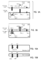
- FIGS. 1, 2A, 2B, 3A, 3B, 3C are vertical cross sectional views of microelectronic components at different stages of fabrication according to prior art.
- FIGS. 4A, 4B, 4C, 5, 6A, 6B, 7A are vertical cross sectional views of microelectronic components at different stages of fabrication according to some embodiments of the present invention.
- FIG. 7B is a top view of a microelectronic component according to some embodiments of the present invention.
- FIGS. 8, 9A, 9B, 10A, 10B, 11, 12A, 12B, 12C, 12D, 13A, 13B, 13C, 13D, 13E, 13F, 14A, 14B, 15, 16 are vertical cross sectional views of microelectronic components at different stages of fabrication according to some embodiments of the present invention.
- Components 110 , 120 , and other microelectronic components described below can be any microelectronic components, not necessarily an IC or an interconnect substrate, unless the context clearly indicates otherwise.
- one or both of components 110 and 120 can be an assembly of multiple ICs and/or interconnect substrates.
- IC and “substrate” are used for illustration and not to limit the invention.
- contact pads 110 C can be connected to circuitry 150 in component 110 .
- Circuitry 150 may include conductive lines (including possibly vias extending through component 110 to provide a contact pad (not shown) on top of the component), transistors, resistors, capacitors, inductors, and/or other circuit elements.
- contact pad 120 C can be connected to such circuitry (not shown) in component 120 .
- Circuitry 150 is omitted from some or all of subsequent drawings.
- top and bottom are for ease of description; the components and other elements can be turned upside down or at any angle during fabrication and subsequent operation.
- any one of contact pads 110 C, 120 C can be protruding, with the other contact pad being recessed.
- Suitable NCF tape materials include polymeric tapes, including dielectric organic polymers, possibly with fillers.
- An example is partially cured (B-stage) epoxy with a silica filler.
- Suitable materials are described in the aforementioned U.S. pre-grant patent application no. 2011/0237028 (Hamazaki et al., Sep. 29, 2011), and U.S. Pat. No. 6,916,684 (Stepniak et al., Jul. 12, 2005).
- the NCF tape can be a multi-layer structure, with one or more layers made of the materials described above, with possible additional solid or non-solid layers.
- the contact pad materials can be as in prior art.
- the contact pads may include outer layers of solder or conductive or anisotropic adhesive, or they can be bonded together without solder or adhesive, by thermocompression for example.
- the solder or adhesive is present, are sometimes described as separate layers in the discussion below, but sometimes are referred to as parts of the contact pads.
- Solder or adhesive can be pre-deposited on contact pad 110 C before the component-to-component attachment. Alternatively or in addition, the solder or adhesive can be pre-deposited on contact pad 120 C either before application of NCF 130 on component 120 , or after NCF application (if, for example, the NCF tape is pre-patterned before the component attachment).
- the operation of FIG. 4C starts at a lower temperature, when the NCF tape 130 is easier to rupture (the NCF fracture strength is lower).
- the temperature is increased; by this time the NCF tape may have been ruptured and the two contact pads are in a position, or almost in a position, in which they can be bonded together (by thermocompression, solder (not shown), conductive or anisotropic adhesive (not shown), or some other means).
- the contact pad 110 C when the contact pad 110 C is deep inside the cavity, the two contact pads may touch or almost touch each other, or they may touch or almost touch a bonding agent such as solder or adhesive.
- Increasing the temperature at this stage may soften the NCF (depending on the NCF material) and thus help remove any NCF residue from between the contact pads. Increased temperature may also be required to bond the contact pads together.
- filling the cavity may be desirable in some embodiments to eliminate air or other gas that could otherwise be trapped inside the cavity and corrode the contact pads. However, it may be desirable not to fill the cavity completely in order to provide room for thermal expansion of solder or other materials during solder reflow performed in attaching the contact pads 110 C to 120 C or for other high temperature operations.
- the protruding contact pad 110 C does not rupture the NCF tape even when the NCF tape contacts the recessed pad 120 C.
- the NCF tape can be ruptured incompletely, with some NCF residue remaining between the contact pads. Additional removal of the NCF residue is performed when NCF is pressed against the recessed contact pad 120 C, similarly to FIG. 3B .
- the NCF tape is stretched and thinned and hence easier to rupture; NCF residue removal is therefore more complete.
- solder or adhesive 610 can be deposited into cavity 410 before application of NCF 130 .
- Solder or adhesive 610 may fill the cavity to a level above the contact pad 120 C, but does not fill the cavity completely, leaving a void 410 V under the NCF tape.
- a reliable bond ( FIG. 6B ) between contact pads 110 C and 120 C can be achieved even if the contact pad 110 C does not reach the contact pad 120 C, as long as the contact pad 110 C reaches the solder or adhesive 610 . Therefore, this architecture is tolerant to variations in the size of contact pads 110 C, the depth of cavity 410 , the amount of solder or adhesive 610 , and the compressive force F applied during the attachment.
- NCF tape 130 can be pre-patterned; FIGS. 7A, 7B show holes 710 formed in NCF 130 at the location of cavities 410 before the component-to-component attachment.
- FIG. 7B is a top view of pre-patterned NCF on component 120
- FIG. 7A shows a vertical cross-section of the component 120 along a vertical plane A-A of FIG. 7B .
- the holes 710 can be made by stamping (using for example a stamp 720 made of steel or polymer (e.g. PDMS) or some other material), or by laser, or photolithographically, or in some other way.
- Some photolithographic embodiments use photoimageable NCF 130 , or a multi-layer NCF having a top photoimageable layer.
- photoimageable underfill materials are certain types of organic polymers such as polyimides and benzocyclobutene (BCB) based polymers available from DuPont, Fujifilm, and other manufactures.
- BCB benzocyclobutene
- a separate photoresist layer can be used on top of NCF 130 , and can be removed after the NCF is patterned and before the component-to-component attachment.
- the holes 710 can be smaller in lateral dimension (in top view) than the cavities 410 or pads 120 C or 110 C.
- protruding contact pads 110 C enlarge the holes, facilitating a reliable contact bond. Therefore, the NCF tape can be stretched by smaller amount during bonding.
- the cavity depth can be reduced (the cavity depth, or rather the depth of void 410 V, defines the maximum strain of the NCF tape). Shallower cavities can be formed faster and more reliably.
- contacts 110 C may be allowed to have shorter protrusions, and thus to be mechanically stronger, resulting in improved reliability and manufacturing yield.
- the compressive force F can be reduced, and there is more tolerance to variations in the force F, the cavity depth, and possibly other parameters (e.g. NCF composition).
- NCF tape 130 can be pre-patterned before its application to component 120 .
- NCF tape 130 is placed on vacuum stage 804 having holes 810 that match the positions of cavities 410 .
- Vacuum pump 820 creates vacuum under holes 810 .
- NCF tape is ruptured at each hole 810 , to form the corresponding hole 710 .
- the NCF can be ruptured by the vacuum force, and/or a stamp (such as 720 shown in FIG. 7A ).
- NCF tape 130 may include a liner on the bottom to allow the NCF tape to be easily detachable from the vacuum stage after the pre-patterning process.
- the patterned NCF tape is then placed on component 120 as in FIG. 7A .
- the NCF can be pre-patterned by laser or photolithographically.
- WUF wafer level underfill
- ICs or stacks of ICs are fabricated in a single wafer or a stack of wafers, and the wafer or stack is then diced to separate the ICs or IC stacks.
- NCF is applied on top of a wafer and is diced together with the wafer; dicing forms individual ICs with the NCF already on top of each IC. See U.S. pre-grant patent application no. 2009/0108472 (Feger et al., Apr. 30, 2009), and Underfilling in the era of high density/3D interconnect: a closer look, I-Micronews, Jan. 3, 2012, both incorporated herein by reference.
- NCF tape 130 is applied on a wafer (on the top wafer of a stack if there is a stack), and NCF tape 130 is diced together with the wafer or stack; the dicing forms individual components 120 with the NCF tape on each component.
- NCF can be pre-patterned before or after application to the wafer or stack (as in FIG. 7A or 8 ), before or after dicing.
- FIGS. 9A and 9B illustrate that the same component may have protruding, recessed, and other types of contact pads.
- FIG. 9A illustrates the components 110 and 120 before they are attached together;
- FIG. 9B illustrates the components after attachment.
- Component 110 has a protruding contact pad 110 C. 1 , a recessed contact pad 110 C. 2 in cavity 410 . 2 , and another contact pad 110 C. 3 .
- Component 120 has respective matching contact pads 120 C. 1 (recessed in cavity 410 . 1 ), 120 C. 2 (protruding), and 120 C. 3 .
- NCF tape 130 A has been applied to component 110 to cover the cavity 410 . 2 , leaving a void 410 V. 2 in the cavity.
- NCF 130 A does not cover contact pads 110 C. 1 and 110 C. 3 .
- Component 120 has NCF tape 130 B covering the cavity 410 . 1 , leaving a void 410 V. 1 in the cavity.
- NCF 130 B does not cover contact pads 120 C. 2 and 120 C. 3 .
- contact pad 110 C. 1 pierces NCF tape 130 B
- contact pad 120 C. 2 pierces NCF tape 130 A, to bond to the corresponding contact pads 120 C. 1 and 110 C. 2 .
- contact pads 110 C. 3 and/or 120 C. 3 can be covered by respective underfill 130 A or 130 B before attachment, and can be joined together by displacing the underfill as in prior art. Other combinations of the features described above are also possible.
- Protruding and recessed contact pads can be formed by many techniques, including prior art techniques. For example, to form a protruding contact pad, one can first form a contact pad of any geometry, and then augment the contact pad with a protruding solder bump or a copper post or some other type of protruding conductor. In some embodiments, protruding contact pads are formed as copper posts (e.g. by electroplating a copper layer using a suitable mask); or as wires bonded to a component. Exemplary protruding wires are BVA wires described in InvensasTM High Performance BVA PoP package for Mobile Systems, May 2013 by Invensas Corporation of San Jose, Calif., incorporated herein by reference; see also U.S. Pat. No.
- Protruding contact pads can also be formed using technology related to through-substrate vias (TSVs); see the aforementioned U.S. Pat. No. 7,049,170.
- TSVs through-substrate vias
- a substrate 910 FIG. 10A
- Conductive vias 920 can be connected to other circuitry (not shown, such as 150 in FIG. 4A ) formed in or above the substrate.
- the substrate can be silicon, glass, or other materials.
- the substrate is thinned from the bottom ( FIG. 10B ), possibly by a blanket etch. Vias 920 become exposed and protrude on the bottom, forming the protruding contact pads shown as 920 C. Additional circuitry can be formed on the bottom if desired.
- Protruding contact pads can have sharp tips to facilitate rupture of NCF 130 .
- a conical or pyramidal shape can be provided, as in FIG. 11 for contact pad 110 C.
- Such shapes can be formed by suitable photolithography, e.g. by image reversal photoresist or other techniques; see e.g. U.S. pre-grant patent publication 2013/0270699 (Kuo et al., Oct. 17, 2013), incorporated herein by reference. In TSV variations, such shapes can be formed by suitable shaping of holes 914 .
- Recessed contact pads can also be formed by known techniques, e.g. forming a contact pad of any geometry, then forming a dielectric layer over the contact pad (possibly with a dielectric with a planar top surface throughout the component), and photolithographically patterning the dielectric layer to form a cavity 410 exposing the contact pad.
- the recessed contact pad protrudes out of the cavity bottom.
- the protrusion can be formed by the techniques described above; for example, the recessed contact pad can first be formed as a protruding contact pad; then a dielectric layer can be deposited to cover the protruding contact pad; then a cavity can be etched in the dielectric to expose the top surface and sidewalls of the contact pad; the contact pad is now recessed in the cavity but protrudes from the cavity bottom.
- Recessed contact pads can also be made by TSV technology.
- blind vias 920 can be formed as in FIG. 10A ; only one via is shown for simplicity, but any number of vias can be formed simultaneously or in sequence.
- a layer 1104 lines the holes 914 and separates the substrate 910 from vias 920 ; layer 1104 is marked as dielectric (e.g. to electrically insulate the vias 920 from the substrate and/or each other); alternatively, or in addition, layer 1104 may function as a barrier layer, or seed layer if conductor 920 was electroplated, and/or may serve other purposes. Layer 1104 is omitted in some embodiments.
- substrate 910 may optionally be thinned from the bottom by a blanket etch without revealing the blind bias 920 .
- a masked etch of the substrate's bottom surface creates cavities 410 around the bottom ends of vias 920 .
- Dielectric 1120 ( FIG. 12C ) is deposited on the bottom surface of the structure to protect and electrically insulate the substrate 910 in subsequent processing.
- Dielectric layers 1104 , 1120 initially covered the via 920 on the bottom, but they have been patterned photolithographically to expose the via 920 on the bottom as shown in FIG. 12C .
- Other layers 1150 FIG.
- the layer 1150 covers the via 920 on the bottom but has an exposed conductive surface underlying the via 920 and providing the recessed contact pad 920 C.
- a recessed contact pad can be provided by some other part of layer 1150 in cavity 410 and/or by via 920 .
- NCF (not shown) can be applied to the bottom surface and processed by any of the techniques described above.
- a recessed contact pad can also be formed at the top of via 920 .
- An exemplary process is shown in FIGS. 13A-13E .
- Cavities 410 FIG. 13A
- the terms “top” and “bottom” are for ease of description; the substrate or other elements can be turned upside down or at any angle during fabrication and subsequent operation).
- a mask 1210 FIG. 13B
- the holes can be blind as shown, or can go through substrate 120 .
- Mask 1210 is removed, and the top surface of substrate 910 is covered by dielectric 1110 ( FIG.
- a mask 1218 ( FIG. 13D ) is formed to cover the structure but expose the holes 914 .
- Conductor 920 e.g. copper, is electroplated to line or fill the holes 914 .
- dielectric 1110 and seed 1214 can be removed or patterned as desired. In the embodiment shown, seed 1214 is removed but dielectric 1110 is left in place; dielectric 1110 may cover the surfaces of cavities 410 .
- the recessed contact pad is provided by the top surface of conductor 920 .
- a circuit layer 1150 can be formed on top to connect conductor 920 to other elements and provide other circuit elements as in FIG. 12D ; in this case, the recessed contact pad can be provided by the circuit layer's portion overlying the conductor 920 .
- Subsequent processing can be as described above. For example, NCF tape can be formed on top.
- substrate 120 can be thinned on the bottom to turn conductor 920 into a TSV and provide a recessed or protruding contact pad on the bottom.
- a protruding contact pad can be provided by a blanket etch as in FIG. 10B .
- the resulting structure is shown in FIG. 14A ; dielectric 1110 is removed at the bottom of via 920 by the blanket or masked etch.
- a circuit layer 1150 FIG. 14B
- the protruding contact pad can be provided by the circuit layer's portion underlying the TSV 920 .
- a recessed contact pad on the bottom of the structure of FIG. 13F can be provided by a process of FIGS. 12B-12D ; the resulting structure is shown in FIG. 15 .
- the TSV technology described above can be used to reduce the height of a microelectronic component that includes a stack of die (such as die 110 . 1 through 110 . 4 ); each die 110 in the middle of the stack has a TSV 920 connected to a TSV 920 of the die above and to another TSV 920 of a die below.
- the stacked TSVs 920 form a vertical wire that can be connected to each die's circuitry. Examples of such stacks are hybrid memory cubes (see e.g. U.S. pre-grant patent publications 2012/0276733, Saeki et al., Nov. 1, 2012, incorporated herein by reference); routing circuits (U.S.
- FIG. 16 shows four dies 110 . 1 through 110 . 4 , with die 110 . 4 not yet attached to the bottom of the stack. Only one TSV wire is shown, composed of the four TSVs of the four die.
- Each die's TSV 920 has the structure of FIG. 14 , i.e. has a recessed contact pad 920 C at the top and a protruding contact pad 920 C at the bottom. The top contact pad of each die (except 110 . 1 ) is bonded to the bottom contact pad of the overlying die to form the wire. Any number of die can be present in the stack.
- TSV wire Only one TSV wire is shown, but any number of TSV wires can be present (e.g. an array of TSV wires can be present).
- the bottom contact pad of the TSV wire (in the bottom die) can be connected to a PCB or some other substrate (not shown).
- the top die may or may not have a contact pad at the top of the TSV wire.
- die 110 . 4 can be attached to the bottom of the stack before it is thinned from the bottom, i.e. at the stage of FIG. 13F (while its via 920 is still a blind via); the die can be thinned from below after the attachment. Each die (other than the top die) can be thinned after the attachment. See U.S. Pat. No. 6,322,903 (Siniaguine et al., Nov. 21, 2001) incorporated herein by reference.
Abstract
Description
Claims (15)
Priority Applications (3)
| Application Number | Priority Date | Filing Date | Title |
|---|---|---|---|
| US14/488,187 US9496154B2 (en) | 2014-09-16 | 2014-09-16 | Use of underfill tape in microelectronic components, and microelectronic components with cavities coupled to through-substrate vias |
| TW104130617A TW201622017A (en) | 2014-09-16 | 2015-09-16 | Use of underfill tape in microelectronic components, and microelectronic components with cavities coupled to through-substrate vias |
| PCT/US2015/050374 WO2016044389A1 (en) | 2014-09-16 | 2015-09-16 | Use of underfill tape in microelectronic components, and microelectronic components with cavities coupled to through-substrate vias |
Applications Claiming Priority (1)
| Application Number | Priority Date | Filing Date | Title |
|---|---|---|---|
| US14/488,187 US9496154B2 (en) | 2014-09-16 | 2014-09-16 | Use of underfill tape in microelectronic components, and microelectronic components with cavities coupled to through-substrate vias |
Publications (2)
| Publication Number | Publication Date |
|---|---|
| US20160079093A1 US20160079093A1 (en) | 2016-03-17 |
| US9496154B2 true US9496154B2 (en) | 2016-11-15 |
Family
ID=54200115
Family Applications (1)
| Application Number | Title | Priority Date | Filing Date |
|---|---|---|---|
| US14/488,187 Active US9496154B2 (en) | 2014-09-16 | 2014-09-16 | Use of underfill tape in microelectronic components, and microelectronic components with cavities coupled to through-substrate vias |
Country Status (3)
| Country | Link |
|---|---|
| US (1) | US9496154B2 (en) |
| TW (1) | TW201622017A (en) |
| WO (1) | WO2016044389A1 (en) |
Cited By (4)
| Publication number | Priority date | Publication date | Assignee | Title |
|---|---|---|---|---|
| US9978710B2 (en) * | 2015-12-24 | 2018-05-22 | Imec Vzw | Method for self-aligned solder reflow bonding and devices obtained thereof |
| US10586716B2 (en) * | 2017-06-09 | 2020-03-10 | Advanced Semiconductor Engineering, Inc. | Semiconductor device package |
| US11133259B2 (en) | 2019-12-12 | 2021-09-28 | International Business Machines Corporation | Multi-chip package structure having high density chip interconnect bridge with embedded power distribution network |
| US20240047344A1 (en) * | 2018-10-22 | 2024-02-08 | Adeia Semiconductor Bonding Technologies Inc. | Interconnect structures |
Families Citing this family (4)
| Publication number | Priority date | Publication date | Assignee | Title |
|---|---|---|---|---|
| JP2019066604A (en) * | 2017-09-29 | 2019-04-25 | 株式会社ジャパンディスプレイ | Display device and manufacturing method thereof |
| US10748844B2 (en) * | 2017-12-30 | 2020-08-18 | Intel Corporation | Stress isolation for silicon photonic applications |
| US20200105646A1 (en) * | 2018-10-01 | 2020-04-02 | Nanya Technology Corporation | Semiconductor structure having through silicon via structure and method for forming the same |
| KR20210053537A (en) * | 2019-11-04 | 2021-05-12 | 삼성전자주식회사 | A semiconductor package |
Citations (57)
| Publication number | Priority date | Publication date | Assignee | Title |
|---|---|---|---|---|
| US5386087A (en) | 1992-02-17 | 1995-01-31 | E. I. Du Pont De Nemours And Company | Printed circuit board having U-shaped solder mask layer separating respective contacts |
| US6137062A (en) | 1998-05-11 | 2000-10-24 | Motorola, Inc. | Ball grid array with recessed solder balls |
| US6157076A (en) | 1997-06-30 | 2000-12-05 | Intersil Corporation | Hermetic thin pack semiconductor device |
| EP1137066A2 (en) | 2000-03-24 | 2001-09-26 | Shinko Electric Industries Co. Ltd. | Semiconductor device and process of production of same |
| US6322903B1 (en) | 1999-12-06 | 2001-11-27 | Tru-Si Technologies, Inc. | Package of integrated circuits and vertical integration |
| US20030134450A1 (en) * | 2002-01-09 | 2003-07-17 | Lee Teck Kheng | Elimination of RDL using tape base flip chip on flex for die stacking |
| US20030183951A1 (en) | 2002-03-29 | 2003-10-02 | Achyuta Achari | Flip-chip bonding method |
| US6717254B2 (en) | 2001-02-22 | 2004-04-06 | Tru-Si Technologies, Inc. | Devices having substrates with opening passing through the substrates and conductors in the openings, and methods of manufacture |
| US20040092141A1 (en) * | 2001-09-07 | 2004-05-13 | Salmon Peter C. | Electronic system modules and method of fabrication |
| US6773958B1 (en) | 2002-10-17 | 2004-08-10 | Altera Corporation | Integrated assembly-underfill flip chip process |
| US6881609B2 (en) | 2001-09-07 | 2005-04-19 | Peter C. Salmon | Component connections using bumps and wells |
| US20050140026A1 (en) | 2001-09-07 | 2005-06-30 | Salmon Peter C. | Fabrication methods for electronic system modules |
| US6916684B2 (en) | 2003-03-18 | 2005-07-12 | Delphi Technologies, Inc. | Wafer-applied underfill process |
| US20050212105A1 (en) | 2004-03-23 | 2005-09-29 | Walk Michael J | Integrated circuit die and substrate coupling |
| US20050255722A1 (en) | 2004-05-07 | 2005-11-17 | Salmon Peter C | Micro blade assembly |
| US20050263869A1 (en) | 2004-05-25 | 2005-12-01 | Renesas Technology Corp. | Semiconductor device and manufacturing process therefor |
| US7049170B2 (en) | 2003-12-17 | 2006-05-23 | Tru-Si Technologies, Inc. | Integrated circuits and packaging substrates with cavities, and attachment methods including insertion of protruding contact pads into cavities |
| US7115988B1 (en) | 2004-01-21 | 2006-10-03 | Altera Corporation | Bypass capacitor embedded flip chip package lid and stiffener |
| US20070007983A1 (en) | 2005-01-06 | 2007-01-11 | Salmon Peter C | Semiconductor wafer tester |
| US7163830B2 (en) | 2004-10-12 | 2007-01-16 | Salmon Peter C | Method for temporarily engaging electronic component for test |
| US20070023923A1 (en) | 2005-08-01 | 2007-02-01 | Salmon Peter C | Flip chip interface including a mixed array of heat bumps and signal bumps |
| US20070023889A1 (en) | 2005-08-01 | 2007-02-01 | Salmon Peter C | Copper substrate with feedthroughs and interconnection circuits |
| US20070178232A1 (en) * | 2001-10-19 | 2007-08-02 | Cabot Corporation | Tape compositions for the deposition of electronic features |
| US7254024B2 (en) | 2004-05-11 | 2007-08-07 | Salmon Peter C | Cooling apparatus and method |
| US20070235850A1 (en) | 2006-04-07 | 2007-10-11 | Gerber Mark A | Packaged system of semiconductor chips having a semiconductor interposer |
| US7408258B2 (en) | 2003-08-20 | 2008-08-05 | Salmon Technologies, Llc | Interconnection circuit and electronic module utilizing same |
| US7427809B2 (en) | 2004-12-16 | 2008-09-23 | Salmon Technologies, Llc | Repairable three-dimensional semiconductor subsystem |
| US7505862B2 (en) | 2003-03-07 | 2009-03-17 | Salmon Technologies, Llc | Apparatus and method for testing electronic systems |
| US20090108472A1 (en) | 2007-10-29 | 2009-04-30 | International Business Machines Corporation | Wafer-level underfill process using over-bump-applied resin |
| US7586747B2 (en) | 2005-08-01 | 2009-09-08 | Salmon Technologies, Llc. | Scalable subsystem architecture having integrated cooling channels |
| US20100047969A1 (en) | 2008-08-20 | 2010-02-25 | Kim Won-Keun | Backgrinding-underfill film, method of forming the same, semiconductor package using the backgrinding-underfill film, and method of forming the semiconductor package |
| US20100059897A1 (en) * | 2008-09-11 | 2010-03-11 | Micron Technology, Inc. | Interconnect structures for stacked dies, including penetrating structures for through-silicon vias, and associated systems and methods |
| US20100276799A1 (en) | 2009-05-04 | 2010-11-04 | Heng Stephen F | Semiconductor Chip Package with Stiffener Frame and Configured Lid |
| US20110027967A1 (en) | 2009-07-08 | 2011-02-03 | Imec | Method for insertion bonding and device thus obtained |
| US20110186998A1 (en) | 2010-02-03 | 2011-08-04 | Albert Wu | Recessed semiconductor substrates |
| US20110215464A1 (en) * | 2009-12-29 | 2011-09-08 | Intel Corporation | Semiconductor package with embedded die and its methods of fabrication |
| US20110233762A1 (en) * | 2010-03-25 | 2011-09-29 | International Business Machines Corporation | Wafer level integrated interconnect decal and manufacturing method thereof |
| US20110237028A1 (en) | 2009-02-27 | 2011-09-29 | Sony Chemical & Information Device Corporation | Method of manufacturing semiconductor device |
| US8071470B2 (en) | 2008-10-23 | 2011-12-06 | Carsem (M) Sdn. Bhd. | Wafer level package using stud bump coated with solder |
| US8106518B2 (en) | 2008-12-19 | 2012-01-31 | Renesas Electronics Corporation | Semiconductor device and method of manufacturing the same |
| US20120106228A1 (en) | 2010-11-03 | 2012-05-03 | Netlist, Inc. | Method and apparatus for optimizing driver load in a memory package |
| US8202797B2 (en) | 2010-06-22 | 2012-06-19 | Stats Chippac Ltd. | Integrated circuit system with recessed through silicon via pads and method of manufacture thereof |
| US20120276733A1 (en) | 2011-04-27 | 2012-11-01 | Elpida Memory, Inc. | Method for manufacturing semiconductor device |
| US20120295415A1 (en) | 2011-05-16 | 2012-11-22 | Elpida Memory, Inc. | Method of manufacturing semiconductor device |
| US20130087917A1 (en) | 2011-10-10 | 2013-04-11 | Young-Kun Jee | Semiconductor package |
| US20130119528A1 (en) | 2011-11-14 | 2013-05-16 | Micron Technology, Inc. | Stacked semiconductor die assemblies with multiple thermal paths and associated systems and methods |
| US20130146991A1 (en) | 2011-12-08 | 2013-06-13 | Infineon Technologies Ag | Device Including Two Power Semiconductor Chips and Manufacturing Thereof |
| US20130196472A1 (en) | 2011-02-01 | 2013-08-01 | Henkel Corporation | Pre-cut wafer applied underfill film on dicing tape |
| US20130214431A1 (en) | 2012-02-16 | 2013-08-22 | Taiwan Semiconductor Manufacturing Company, Ltd. | Fine-Pitch Package-on-Package Structures and Methods for Forming the Same |
| US20130241026A1 (en) | 2012-03-17 | 2013-09-19 | Zvi Or-Bach | Novel semiconductor device and structure |
| US20130267046A1 (en) | 2012-04-09 | 2013-10-10 | Zvi Or-Bach | Method for fabrication of a semiconductor device and structure |
| US20130270699A1 (en) | 2012-04-17 | 2013-10-17 | Taiwan Semiconductor Manufacturing Company, Ltd. | Conical-Shaped or Tier-Shaped Pillar Connections |
| US20130292840A1 (en) | 2011-12-02 | 2013-11-07 | Kenneth Shoemaker | Stacked memory allowing variance in device interconnects |
| US8618659B2 (en) | 2011-05-03 | 2013-12-31 | Tessera, Inc. | Package-on-package assembly with wire bonds to encapsulation surface |
| US20140036454A1 (en) | 2012-08-03 | 2014-02-06 | Invensas Corporation | Bva interposer |
| US20140111269A1 (en) | 2012-10-24 | 2014-04-24 | National Changhua University Of Education | Through-silicon via self-routing circuit and routing method thereof |
| US20140239507A1 (en) * | 2013-02-27 | 2014-08-28 | Taiwan Semiconductor Manufacturing Company, Ltd. | Peripheral Electrical Connection of Package on Package |
-
2014
- 2014-09-16 US US14/488,187 patent/US9496154B2/en active Active
-
2015
- 2015-09-16 WO PCT/US2015/050374 patent/WO2016044389A1/en active Application Filing
- 2015-09-16 TW TW104130617A patent/TW201622017A/en unknown
Patent Citations (61)
| Publication number | Priority date | Publication date | Assignee | Title |
|---|---|---|---|---|
| US5386087A (en) | 1992-02-17 | 1995-01-31 | E. I. Du Pont De Nemours And Company | Printed circuit board having U-shaped solder mask layer separating respective contacts |
| US6157076A (en) | 1997-06-30 | 2000-12-05 | Intersil Corporation | Hermetic thin pack semiconductor device |
| US6137062A (en) | 1998-05-11 | 2000-10-24 | Motorola, Inc. | Ball grid array with recessed solder balls |
| US6322903B1 (en) | 1999-12-06 | 2001-11-27 | Tru-Si Technologies, Inc. | Package of integrated circuits and vertical integration |
| EP1137066A2 (en) | 2000-03-24 | 2001-09-26 | Shinko Electric Industries Co. Ltd. | Semiconductor device and process of production of same |
| US20010026010A1 (en) * | 2000-03-24 | 2001-10-04 | Michio Horiuchi | Semiconductor device and process of production of same |
| US6717254B2 (en) | 2001-02-22 | 2004-04-06 | Tru-Si Technologies, Inc. | Devices having substrates with opening passing through the substrates and conductors in the openings, and methods of manufacture |
| US7297572B2 (en) | 2001-09-07 | 2007-11-20 | Hynix Semiconductor, Inc. | Fabrication method for electronic system modules |
| US20040092141A1 (en) * | 2001-09-07 | 2004-05-13 | Salmon Peter C. | Electronic system modules and method of fabrication |
| US6927471B2 (en) | 2001-09-07 | 2005-08-09 | Peter C. Salmon | Electronic system modules and method of fabrication |
| US6881609B2 (en) | 2001-09-07 | 2005-04-19 | Peter C. Salmon | Component connections using bumps and wells |
| US20050140026A1 (en) | 2001-09-07 | 2005-06-30 | Salmon Peter C. | Fabrication methods for electronic system modules |
| US20070178232A1 (en) * | 2001-10-19 | 2007-08-02 | Cabot Corporation | Tape compositions for the deposition of electronic features |
| US20030134450A1 (en) * | 2002-01-09 | 2003-07-17 | Lee Teck Kheng | Elimination of RDL using tape base flip chip on flex for die stacking |
| US20030183951A1 (en) | 2002-03-29 | 2003-10-02 | Achyuta Achari | Flip-chip bonding method |
| US6773958B1 (en) | 2002-10-17 | 2004-08-10 | Altera Corporation | Integrated assembly-underfill flip chip process |
| US7505862B2 (en) | 2003-03-07 | 2009-03-17 | Salmon Technologies, Llc | Apparatus and method for testing electronic systems |
| US6916684B2 (en) | 2003-03-18 | 2005-07-12 | Delphi Technologies, Inc. | Wafer-applied underfill process |
| US7408258B2 (en) | 2003-08-20 | 2008-08-05 | Salmon Technologies, Llc | Interconnection circuit and electronic module utilizing same |
| US7049170B2 (en) | 2003-12-17 | 2006-05-23 | Tru-Si Technologies, Inc. | Integrated circuits and packaging substrates with cavities, and attachment methods including insertion of protruding contact pads into cavities |
| US7115988B1 (en) | 2004-01-21 | 2006-10-03 | Altera Corporation | Bypass capacitor embedded flip chip package lid and stiffener |
| US20050212105A1 (en) | 2004-03-23 | 2005-09-29 | Walk Michael J | Integrated circuit die and substrate coupling |
| US20050255722A1 (en) | 2004-05-07 | 2005-11-17 | Salmon Peter C | Micro blade assembly |
| US7254024B2 (en) | 2004-05-11 | 2007-08-07 | Salmon Peter C | Cooling apparatus and method |
| US20050263869A1 (en) | 2004-05-25 | 2005-12-01 | Renesas Technology Corp. | Semiconductor device and manufacturing process therefor |
| US7163830B2 (en) | 2004-10-12 | 2007-01-16 | Salmon Peter C | Method for temporarily engaging electronic component for test |
| US7427809B2 (en) | 2004-12-16 | 2008-09-23 | Salmon Technologies, Llc | Repairable three-dimensional semiconductor subsystem |
| US20070007983A1 (en) | 2005-01-06 | 2007-01-11 | Salmon Peter C | Semiconductor wafer tester |
| US20070023889A1 (en) | 2005-08-01 | 2007-02-01 | Salmon Peter C | Copper substrate with feedthroughs and interconnection circuits |
| US20070023923A1 (en) | 2005-08-01 | 2007-02-01 | Salmon Peter C | Flip chip interface including a mixed array of heat bumps and signal bumps |
| US7586747B2 (en) | 2005-08-01 | 2009-09-08 | Salmon Technologies, Llc. | Scalable subsystem architecture having integrated cooling channels |
| US20070235850A1 (en) | 2006-04-07 | 2007-10-11 | Gerber Mark A | Packaged system of semiconductor chips having a semiconductor interposer |
| US20090108472A1 (en) | 2007-10-29 | 2009-04-30 | International Business Machines Corporation | Wafer-level underfill process using over-bump-applied resin |
| US20100047969A1 (en) | 2008-08-20 | 2010-02-25 | Kim Won-Keun | Backgrinding-underfill film, method of forming the same, semiconductor package using the backgrinding-underfill film, and method of forming the semiconductor package |
| US20100059897A1 (en) * | 2008-09-11 | 2010-03-11 | Micron Technology, Inc. | Interconnect structures for stacked dies, including penetrating structures for through-silicon vias, and associated systems and methods |
| US8071470B2 (en) | 2008-10-23 | 2011-12-06 | Carsem (M) Sdn. Bhd. | Wafer level package using stud bump coated with solder |
| US20120091583A1 (en) | 2008-12-19 | 2012-04-19 | Kawashita Michihiro | Semiconductor device and method of manufacturing the same |
| US8106518B2 (en) | 2008-12-19 | 2012-01-31 | Renesas Electronics Corporation | Semiconductor device and method of manufacturing the same |
| US20110237028A1 (en) | 2009-02-27 | 2011-09-29 | Sony Chemical & Information Device Corporation | Method of manufacturing semiconductor device |
| US20100276799A1 (en) | 2009-05-04 | 2010-11-04 | Heng Stephen F | Semiconductor Chip Package with Stiffener Frame and Configured Lid |
| US20110027967A1 (en) | 2009-07-08 | 2011-02-03 | Imec | Method for insertion bonding and device thus obtained |
| US20110215464A1 (en) * | 2009-12-29 | 2011-09-08 | Intel Corporation | Semiconductor package with embedded die and its methods of fabrication |
| US20110186998A1 (en) | 2010-02-03 | 2011-08-04 | Albert Wu | Recessed semiconductor substrates |
| US20110233762A1 (en) * | 2010-03-25 | 2011-09-29 | International Business Machines Corporation | Wafer level integrated interconnect decal and manufacturing method thereof |
| US8202797B2 (en) | 2010-06-22 | 2012-06-19 | Stats Chippac Ltd. | Integrated circuit system with recessed through silicon via pads and method of manufacture thereof |
| US20120106228A1 (en) | 2010-11-03 | 2012-05-03 | Netlist, Inc. | Method and apparatus for optimizing driver load in a memory package |
| US20130196472A1 (en) | 2011-02-01 | 2013-08-01 | Henkel Corporation | Pre-cut wafer applied underfill film on dicing tape |
| US20120276733A1 (en) | 2011-04-27 | 2012-11-01 | Elpida Memory, Inc. | Method for manufacturing semiconductor device |
| US8618659B2 (en) | 2011-05-03 | 2013-12-31 | Tessera, Inc. | Package-on-package assembly with wire bonds to encapsulation surface |
| US20120295415A1 (en) | 2011-05-16 | 2012-11-22 | Elpida Memory, Inc. | Method of manufacturing semiconductor device |
| US20130087917A1 (en) | 2011-10-10 | 2013-04-11 | Young-Kun Jee | Semiconductor package |
| US20130119528A1 (en) | 2011-11-14 | 2013-05-16 | Micron Technology, Inc. | Stacked semiconductor die assemblies with multiple thermal paths and associated systems and methods |
| US20130292840A1 (en) | 2011-12-02 | 2013-11-07 | Kenneth Shoemaker | Stacked memory allowing variance in device interconnects |
| US20130146991A1 (en) | 2011-12-08 | 2013-06-13 | Infineon Technologies Ag | Device Including Two Power Semiconductor Chips and Manufacturing Thereof |
| US20130214431A1 (en) | 2012-02-16 | 2013-08-22 | Taiwan Semiconductor Manufacturing Company, Ltd. | Fine-Pitch Package-on-Package Structures and Methods for Forming the Same |
| US20130241026A1 (en) | 2012-03-17 | 2013-09-19 | Zvi Or-Bach | Novel semiconductor device and structure |
| US20130267046A1 (en) | 2012-04-09 | 2013-10-10 | Zvi Or-Bach | Method for fabrication of a semiconductor device and structure |
| US20130270699A1 (en) | 2012-04-17 | 2013-10-17 | Taiwan Semiconductor Manufacturing Company, Ltd. | Conical-Shaped or Tier-Shaped Pillar Connections |
| US20140036454A1 (en) | 2012-08-03 | 2014-02-06 | Invensas Corporation | Bva interposer |
| US20140111269A1 (en) | 2012-10-24 | 2014-04-24 | National Changhua University Of Education | Through-silicon via self-routing circuit and routing method thereof |
| US20140239507A1 (en) * | 2013-02-27 | 2014-08-28 | Taiwan Semiconductor Manufacturing Company, Ltd. | Peripheral Electrical Connection of Package on Package |
Non-Patent Citations (18)
| Title |
|---|
| Cook; Kathy et al., "TSV Processing and Wafer Stacking," SUSS MicroTec, retrieved Sep. 16, 2014, 36 pages. |
| Freescale, "Flip Chip Plastic Ball Grid Array (FC-PBGA)," Application Note, Q2 2012, 55 pages. |
| Gilleo; Dr. Ken et al., The Great Underfill Race retrieved Sep. 16, 2014, 6 pages. |
| Gosele; U. et al., "History and Future of Semiconductor Wafer Bonding," Solid State Phenomena vols. 47-48 (1996) pp. 33-44. |
| Gotro, Jeffrey, "Polymer Challenges in Electronic Packaging: Part 4 Wafer Level Underfills," Polymer Innovation Blog, Oct. 28, 2013, 4 pages. |
| I-Micronews, "Advanced Packaging: Underfilling in the era of high density / 3D interconnect: a closer look," online news article dated Jan. 3, 2012, 5 pages, retrieved 8/15/14. http://www.i-micronews.com/news/Underfilling-era-high-density-3D-interconnect-closer-look,8105.html[Aug. 15, 2014 9:07:22 AM]. |
| International Search Report and Written Opinion issued in PCT Application PCT/US2015/050374 on Jan. 4, 2016. |
| InvensasTM White Paper, "High Performance BVA PoP package for Mobile Systems," May 2013 by Invensas Corporation of San Jose, CA. |
| IP Strategy, "Benefits of Copper Pillar Well (CPW) Technology," Technology/IP Preview, 2006, 4 pages. |
| Johnson; Wayne et al., "Wafer Applied Underfills for Flip Chip Assembly," retrieved Sep. 16, 2014,11 pages. |
| Liang; Di et al., "Low-Temperature, Strong SiO2-SiO2 Covalent Wafer Bonding for III-V Compound Semiconductors-to-Silicon Photonic Integrated Circuits," Journal of Electronic Materials, DOI: 10.1007/s11664-008-0489-1, May 9, 2008, 8 pages. |
| Morita; Akira et al., "Wafer Spray Coating for Pre-Applied Underfill," product flyer by Nordson ASYMTEK dated Nov. 2012, 6 pages. |
| R.H. Esser, et. al., Improved Low-Temperature Si Si Hydrophilic Wafer Bonding, J. Electrochem. Soc. 2003 150(3): G228-G231. |
| Schmidt; Martin A., "Wafer-to-Wafer Bonding for Microstructure Formation," Invited Paper, Proceedings of the IEEE, vol. 86, No. 8, Aug. 1998, 11 pages. |
| Takagi; Hideki et al., "Low Temperature Direct Bonding of Silicon and Silicon Dioxide by the Surface Activation Method," 1997 International Conference on Solid-State Sensors and Actuators Chicago, Jun. 16-19, 1997, pp. 657-660. |
| U.S. Appl. No. 13/924,002, filed Jun. 21, 2013 entitled, "Reliable Device Assembly," by Haba et al. |
| W. P. Maszara, Silicon-On-Insulator by Wafer Bonding: A Review, J. Electrochem. Soc. 1991138(1): 341-347. |
| Zoschke; K. et al., "Polyimide Based Temporary Wafer Bonding Technology for High Temperature Compliant TSV Backside Processing and Thin Device Handling," SUSS MicroTec, Published in the SUSS report Feb. 2012, 11 pages. |
Cited By (5)
| Publication number | Priority date | Publication date | Assignee | Title |
|---|---|---|---|---|
| US9978710B2 (en) * | 2015-12-24 | 2018-05-22 | Imec Vzw | Method for self-aligned solder reflow bonding and devices obtained thereof |
| US10586716B2 (en) * | 2017-06-09 | 2020-03-10 | Advanced Semiconductor Engineering, Inc. | Semiconductor device package |
| US11164756B2 (en) | 2017-06-09 | 2021-11-02 | Advanced Semiconductor Engineering, Inc. | Semiconductor device package having continously formed tapered protrusions |
| US20240047344A1 (en) * | 2018-10-22 | 2024-02-08 | Adeia Semiconductor Bonding Technologies Inc. | Interconnect structures |
| US11133259B2 (en) | 2019-12-12 | 2021-09-28 | International Business Machines Corporation | Multi-chip package structure having high density chip interconnect bridge with embedded power distribution network |
Also Published As
| Publication number | Publication date |
|---|---|
| WO2016044389A1 (en) | 2016-03-24 |
| US20160079093A1 (en) | 2016-03-17 |
| TW201622017A (en) | 2016-06-16 |
Similar Documents
| Publication | Publication Date | Title |
|---|---|---|
| US9496154B2 (en) | Use of underfill tape in microelectronic components, and microelectronic components with cavities coupled to through-substrate vias | |
| CN106952833B (en) | Method and structure for three-dimensional chip stacking | |
| CN110970407B (en) | Integrated circuit package and method | |
| CN107665887B (en) | Package structure and method for forming the same | |
| US9368474B2 (en) | Manufacturing method for semiconductor device | |
| JP5052130B2 (en) | Semiconductor device having three-dimensional laminated structure and method for manufacturing the same | |
| US7691672B2 (en) | Substrate treating method and method of manufacturing semiconductor apparatus | |
| US7498200B2 (en) | Electronic-parts-packaging structure in which a semiconductor chip is mounted on a wiring substrate and buried in an insulation film | |
| US20070045836A1 (en) | Stacked chip package using warp preventing insulative material and manufacturing method thereof | |
| KR102453507B1 (en) | Semiconductor die package and method of manufacture | |
| KR102585621B1 (en) | Integrated circuit package and method | |
| CN108231716B (en) | Package structure and method for manufacturing the same | |
| KR102647008B1 (en) | Fan-out packages and methods of forming the same | |
| TWI550737B (en) | Chip package and method thereof | |
| CN112687670B (en) | Integrated circuit structure and forming method thereof | |
| JP2013021058A (en) | Manufacturing method of semiconductor device | |
| CN111261608B (en) | Semiconductor device and method of forming the same | |
| US9263376B2 (en) | Chip interposer, semiconductor device, and method for manufacturing a semiconductor device | |
| CN113223970B (en) | Semiconductor structure and manufacturing method thereof | |
| KR102540531B1 (en) | Semiconductor package and method of manufacturing the same | |
| CN114927425A (en) | Integrated circuit package and method of formation | |
| CN116247030A (en) | Device package and method thereof | |
| US11297717B2 (en) | Power decoupling attachment | |
| US11133283B2 (en) | Integrated fan-out device | |
| CN116779556A (en) | Semiconductor package and method of forming the same |
Legal Events
| Date | Code | Title | Description |
|---|---|---|---|
| AS | Assignment |
Owner name: INVENSAS CORPORATION, CALIFORNIA Free format text: ASSIGNMENT OF ASSIGNORS INTEREST;ASSIGNORS:KATKAR, RAJESH;WANG, LIANG;UZOH, CYPRIAN EMEKA;AND OTHERS;REEL/FRAME:033753/0077 Effective date: 20140916 |
|
| STCF | Information on status: patent grant |
Free format text: PATENTED CASE |
|
| AS | Assignment |
Owner name: ROYAL BANK OF CANADA, AS COLLATERAL AGENT, CANADA Free format text: SECURITY INTEREST;ASSIGNORS:INVENSAS CORPORATION;TESSERA, INC.;TESSERA ADVANCED TECHNOLOGIES, INC.;AND OTHERS;REEL/FRAME:040797/0001 Effective date: 20161201 |
|
| MAFP | Maintenance fee payment |
Free format text: PAYMENT OF MAINTENANCE FEE, 4TH YEAR, LARGE ENTITY (ORIGINAL EVENT CODE: M1551); ENTITY STATUS OF PATENT OWNER: LARGE ENTITY Year of fee payment: 4 |
|
| AS | Assignment |
Owner name: BANK OF AMERICA, N.A., NORTH CAROLINA Free format text: SECURITY INTEREST;ASSIGNORS:ROVI SOLUTIONS CORPORATION;ROVI TECHNOLOGIES CORPORATION;ROVI GUIDES, INC.;AND OTHERS;REEL/FRAME:053468/0001 Effective date: 20200601 |
|
| AS | Assignment |
Owner name: PHORUS, INC., CALIFORNIA Free format text: RELEASE BY SECURED PARTY;ASSIGNOR:ROYAL BANK OF CANADA;REEL/FRAME:052920/0001 Effective date: 20200601 Owner name: INVENSAS BONDING TECHNOLOGIES, INC. (F/K/A ZIPTRONIX, INC.), CALIFORNIA Free format text: RELEASE BY SECURED PARTY;ASSIGNOR:ROYAL BANK OF CANADA;REEL/FRAME:052920/0001 Effective date: 20200601 Owner name: DTS, INC., CALIFORNIA Free format text: RELEASE BY SECURED PARTY;ASSIGNOR:ROYAL BANK OF CANADA;REEL/FRAME:052920/0001 Effective date: 20200601 Owner name: INVENSAS CORPORATION, CALIFORNIA Free format text: RELEASE BY SECURED PARTY;ASSIGNOR:ROYAL BANK OF CANADA;REEL/FRAME:052920/0001 Effective date: 20200601 Owner name: FOTONATION CORPORATION (F/K/A DIGITALOPTICS CORPORATION AND F/K/A DIGITALOPTICS CORPORATION MEMS), CALIFORNIA Free format text: RELEASE BY SECURED PARTY;ASSIGNOR:ROYAL BANK OF CANADA;REEL/FRAME:052920/0001 Effective date: 20200601 Owner name: IBIQUITY DIGITAL CORPORATION, MARYLAND Free format text: RELEASE BY SECURED PARTY;ASSIGNOR:ROYAL BANK OF CANADA;REEL/FRAME:052920/0001 Effective date: 20200601 Owner name: DTS LLC, CALIFORNIA Free format text: RELEASE BY SECURED PARTY;ASSIGNOR:ROYAL BANK OF CANADA;REEL/FRAME:052920/0001 Effective date: 20200601 Owner name: TESSERA ADVANCED TECHNOLOGIES, INC, CALIFORNIA Free format text: RELEASE BY SECURED PARTY;ASSIGNOR:ROYAL BANK OF CANADA;REEL/FRAME:052920/0001 Effective date: 20200601 Owner name: TESSERA, INC., CALIFORNIA Free format text: RELEASE BY SECURED PARTY;ASSIGNOR:ROYAL BANK OF CANADA;REEL/FRAME:052920/0001 Effective date: 20200601 |