US9491852B2 - Trace border routing - Google Patents
Trace border routing Download PDFInfo
- Publication number
- US9491852B2 US9491852B2 US13/007,493 US201113007493A US9491852B2 US 9491852 B2 US9491852 B2 US 9491852B2 US 201113007493 A US201113007493 A US 201113007493A US 9491852 B2 US9491852 B2 US 9491852B2
- Authority
- US
- United States
- Prior art keywords
- conductive traces
- traces
- trace
- widths
- display
- Prior art date
- Legal status (The legal status is an assumption and is not a legal conclusion. Google has not performed a legal analysis and makes no representation as to the accuracy of the status listed.)
- Active, expires
Links
Images


Classifications
-
- G—PHYSICS
- G06—COMPUTING; CALCULATING OR COUNTING
- G06F—ELECTRIC DIGITAL DATA PROCESSING
- G06F3/00—Input arrangements for transferring data to be processed into a form capable of being handled by the computer; Output arrangements for transferring data from processing unit to output unit, e.g. interface arrangements
- G06F3/01—Input arrangements or combined input and output arrangements for interaction between user and computer
- G06F3/03—Arrangements for converting the position or the displacement of a member into a coded form
- G06F3/041—Digitisers, e.g. for touch screens or touch pads, characterised by the transducing means
- G06F3/0416—Control or interface arrangements specially adapted for digitisers
- G06F3/04164—Connections between sensors and controllers, e.g. routing lines between electrodes and connection pads
-
- H—ELECTRICITY
- H05—ELECTRIC TECHNIQUES NOT OTHERWISE PROVIDED FOR
- H05K—PRINTED CIRCUITS; CASINGS OR CONSTRUCTIONAL DETAILS OF ELECTRIC APPARATUS; MANUFACTURE OF ASSEMBLAGES OF ELECTRICAL COMPONENTS
- H05K1/00—Printed circuits
- H05K1/02—Details
- H05K1/0213—Electrical arrangements not otherwise provided for
- H05K1/0263—High current adaptations, e.g. printed high current conductors or using auxiliary non-printed means; Fine and coarse circuit patterns on one circuit board
- H05K1/0265—High current adaptations, e.g. printed high current conductors or using auxiliary non-printed means; Fine and coarse circuit patterns on one circuit board characterized by the lay-out of or details of the printed conductors, e.g. reinforced conductors, redundant conductors, conductors having different cross-sections
-
- G—PHYSICS
- G06—COMPUTING; CALCULATING OR COUNTING
- G06F—ELECTRIC DIGITAL DATA PROCESSING
- G06F3/00—Input arrangements for transferring data to be processed into a form capable of being handled by the computer; Output arrangements for transferring data from processing unit to output unit, e.g. interface arrangements
- G06F3/01—Input arrangements or combined input and output arrangements for interaction between user and computer
- G06F3/03—Arrangements for converting the position or the displacement of a member into a coded form
- G06F3/041—Digitisers, e.g. for touch screens or touch pads, characterised by the transducing means
- G06F3/0412—Digitisers structurally integrated in a display
-
- G—PHYSICS
- G06—COMPUTING; CALCULATING OR COUNTING
- G06F—ELECTRIC DIGITAL DATA PROCESSING
- G06F3/00—Input arrangements for transferring data to be processed into a form capable of being handled by the computer; Output arrangements for transferring data from processing unit to output unit, e.g. interface arrangements
- G06F3/01—Input arrangements or combined input and output arrangements for interaction between user and computer
- G06F3/03—Arrangements for converting the position or the displacement of a member into a coded form
- G06F3/041—Digitisers, e.g. for touch screens or touch pads, characterised by the transducing means
- G06F3/0416—Control or interface arrangements specially adapted for digitisers
-
- H—ELECTRICITY
- H05—ELECTRIC TECHNIQUES NOT OTHERWISE PROVIDED FOR
- H05K—PRINTED CIRCUITS; CASINGS OR CONSTRUCTIONAL DETAILS OF ELECTRIC APPARATUS; MANUFACTURE OF ASSEMBLAGES OF ELECTRICAL COMPONENTS
- H05K1/00—Printed circuits
- H05K1/02—Details
- H05K1/0213—Electrical arrangements not otherwise provided for
- H05K1/0237—High frequency adaptations
- H05K1/0242—Structural details of individual signal conductors, e.g. related to the skin effect
-
- G—PHYSICS
- G06—COMPUTING; CALCULATING OR COUNTING
- G06F—ELECTRIC DIGITAL DATA PROCESSING
- G06F2203/00—Indexing scheme relating to G06F3/00 - G06F3/048
- G06F2203/041—Indexing scheme relating to G06F3/041 - G06F3/045
- G06F2203/04108—Touchless 2D- digitiser, i.e. digitiser detecting the X/Y position of the input means, finger or stylus, also when it does not touch, but is proximate to the digitiser's interaction surface without distance measurement in the Z direction
-
- G—PHYSICS
- G09—EDUCATION; CRYPTOGRAPHY; DISPLAY; ADVERTISING; SEALS
- G09G—ARRANGEMENTS OR CIRCUITS FOR CONTROL OF INDICATING DEVICES USING STATIC MEANS TO PRESENT VARIABLE INFORMATION
- G09G3/00—Control arrangements or circuits, of interest only in connection with visual indicators other than cathode-ray tubes
- G09G3/20—Control arrangements or circuits, of interest only in connection with visual indicators other than cathode-ray tubes for presentation of an assembly of a number of characters, e.g. a page, by composing the assembly by combination of individual elements arranged in a matrix no fixed position being assigned to or needed to be assigned to the individual characters or partial characters
- G09G3/2092—Details of a display terminals using a flat panel, the details relating to the control arrangement of the display terminal and to the interfaces thereto
-
- H—ELECTRICITY
- H05—ELECTRIC TECHNIQUES NOT OTHERWISE PROVIDED FOR
- H05K—PRINTED CIRCUITS; CASINGS OR CONSTRUCTIONAL DETAILS OF ELECTRIC APPARATUS; MANUFACTURE OF ASSEMBLAGES OF ELECTRICAL COMPONENTS
- H05K2201/00—Indexing scheme relating to printed circuits covered by H05K1/00
- H05K2201/07—Electric details
- H05K2201/0776—Resistance and impedance
- H05K2201/0784—Uniform resistance, i.e. equalizing the resistance of a number of conductors
-
- H—ELECTRICITY
- H05—ELECTRIC TECHNIQUES NOT OTHERWISE PROVIDED FOR
- H05K—PRINTED CIRCUITS; CASINGS OR CONSTRUCTIONAL DETAILS OF ELECTRIC APPARATUS; MANUFACTURE OF ASSEMBLAGES OF ELECTRICAL COMPONENTS
- H05K2201/00—Indexing scheme relating to printed circuits covered by H05K1/00
- H05K2201/09—Shape and layout
- H05K2201/09209—Shape and layout details of conductors
- H05K2201/09218—Conductive traces
- H05K2201/09272—Layout details of angles or corners
-
- H—ELECTRICITY
- H05—ELECTRIC TECHNIQUES NOT OTHERWISE PROVIDED FOR
- H05K—PRINTED CIRCUITS; CASINGS OR CONSTRUCTIONAL DETAILS OF ELECTRIC APPARATUS; MANUFACTURE OF ASSEMBLAGES OF ELECTRICAL COMPONENTS
- H05K2201/00—Indexing scheme relating to printed circuits covered by H05K1/00
- H05K2201/09—Shape and layout
- H05K2201/09209—Shape and layout details of conductors
- H05K2201/09654—Shape and layout details of conductors covering at least two types of conductors provided for in H05K2201/09218 - H05K2201/095
- H05K2201/09727—Varying width along a single conductor; Conductors or pads having different widths
-
- Y—GENERAL TAGGING OF NEW TECHNOLOGICAL DEVELOPMENTS; GENERAL TAGGING OF CROSS-SECTIONAL TECHNOLOGIES SPANNING OVER SEVERAL SECTIONS OF THE IPC; TECHNICAL SUBJECTS COVERED BY FORMER USPC CROSS-REFERENCE ART COLLECTIONS [XRACs] AND DIGESTS
- Y10—TECHNICAL SUBJECTS COVERED BY FORMER USPC
- Y10T—TECHNICAL SUBJECTS COVERED BY FORMER US CLASSIFICATION
- Y10T29/00—Metal working
- Y10T29/49—Method of mechanical manufacture
- Y10T29/49002—Electrical device making
- Y10T29/49117—Conductor or circuit manufacturing
- Y10T29/49124—On flat or curved insulated base, e.g., printed circuit, etc.
- Y10T29/49155—Manufacturing circuit on or in base
Definitions
- This relates generally to conductive traces and more particularly to improved routing of conductive traces in a border area of a device.
- Displays can display graphics and/or text information to a user.
- Touch sensor panels can sense an object, e.g., the user's hand, touching or hovering over the panel, causing the computing system to perform some operation based on the touch or hover.
- Touch screens can include both a display and a touch sensor panel and can allow a user to perform various functions by touching or hovering over the touch sensor panel at a location dictated by a user interface (UI) being displayed by the display, causing the computing system to perform some operation based on the touch or hover and in accordance with the graphics and/or text information appearing at the time of the touch or hover.
- UI user interface
- Portable computing systems are becoming increasingly popular because of their ease and versatility of operation, mobility, and declining price. As such, it is desirable to produce a smaller, thinner system, while maintaining easy and versatile operation.
- the conductive traces can form a staggered stair-step configuration in which the average widths of the traces can be different from each other and each trace can have segments with different widths.
- the conductive traces can be coupled to an active area of the device to transmit signals to and from the active area in accordance with an operation of the device.
- the varying widths can help improve the border area space usage, reduce trace resistance, and reduce the differences in resistance between traces.
- This border routing can advantageously provide smaller border areas and improved device performance.
- FIG. 1 illustrates an exemplary device having border routing of conductive traces according to various embodiments.
- FIG. 2 illustrates an exemplary border routing of the conductive traces of FIG. 1 according to various embodiments.
- FIG. 3 illustrates an exemplary touch screen having border routing of common electrode voltage lines according to various embodiments.
- FIG. 4 illustrates an exemplary touch sensor panel having border routing of stimulation signal lines according to various embodiments.
- FIG. 5 illustrates an exemplary display having border routing of AC common electrode voltage lines according to various embodiments.
- FIG. 6 illustrates an exemplary one chip display having border routing of gate signal lines according to various embodiments.
- FIG. 7 illustrates an exemplary display with gate drivers having border routing of gate driver control lines according to various embodiments.
- FIG. 8 illustrates an exemplary border routing of the conductive traces of FIG. 1 with extended distal ends according to various embodiments.
- FIGS. 9 a through 9 c illustrate exemplary stackups of conductive traces that can have border routing according to various embodiments.
- FIG. 10 illustrates an exemplary mobile telephone having a display that includes border routing of conductive traces according to various embodiments.
- FIG. 11 illustrates an exemplary digital media player having a display that includes border routing of conductive traces according to various embodiments.
- FIG. 12 illustrates an exemplary personal computer having a display that includes border routing of conductive traces according to various embodiments.
- the conductive traces can form a staggered stair-step configuration in which the average widths of the traces can be different from each other and each trace can have segments with different widths.
- the conductive traces can be coupled to an active area of the device to transmit signals to and from the active area in accordance with a device operation.
- the varying widths can help optimize or improve the border area space usage, minimize or reduce trace resistance, and minimize or reduce the differences in resistance between traces.
- This border routing can advantageously provide smaller border areas and improved device performance.
- FIG. 1 illustrates an exemplary device having border routing of conductive traces according to various embodiments.
- electronic device 100 can include active area 110 for performing an operation of the device and border area 120 for routing conductive traces 102 between the active area and signal processing circuitry (not shown).
- the conductive traces 102 can transmit electrical signals to and from the active area 110 in association with the performing operation.
- Each conductive trace 102 can be coupled to a particular location of the active area 110 and routed in the border area 120 from that location to the signal processing circuitry.
- conductive traces 102 - a , 102 - f can be coupled to location A of the active area 110 to transmit signals to and from this location and can be routed in the border area 120 to the signal processing circuitry, which is disposed above location E in this example.
- Conductive traces 102 - b , 102 - g can be coupled to location B of the active area 110 to transmit signals to and from this location and can be in the border area 120 from this location up to the signal processing circuitry.
- Conductive traces 102 - c , 102 - h can be coupled to location C of the active area 110 to transmit signals to and from this location and can be routed in the border area 120 from this location up to the signal processing circuitry.
- Conductive traces 102 - d , 102 - i can be coupled to location D of the active area 110 to transmit signals to and from this location and can be routed in the border area 120 from this location up to the signal processing circuitry.
- Conductive traces 102 - e , 102 - j can be coupled to location E of the active area 110 to transmit signals to and from this location and can be routed in the border area 120 from this location up to the signal processing circuitry.
- Trace resistance can be a function of trace width. Generally, the wider the conductive trace, the lower the resistance. In this example, each trace can be formed to have segments with various widths to reduce the trace's resistance. Trace resistance can also be a function of trace length. Generally, the longer the conductive trace, the higher the resistance. In this example, conductive traces 102 - a , 102 - f are the longest traces, conductive traces 102 - e , 102 - j are the shortest traces, and the other conductive traces have lengths therebetween.
- the widths of the conductive traces 102 can be formed to substantially reduce or eliminate the differences in resistance between the traces.
- the segment widths in each trace can be formed to be different from the segment widths in another trace based on how much resistance difference needs to be reduced or eliminated.
- the trace widths can also be formed to make optimal use of the width of the border area 120 in accordance with the number of traces present at any location along the length of the border area. Accordingly, the trace widths can be formed to reduce the trace's resistance, minimize resistance differences between traces, and optimize border area space for the traces and any other electrical requirements.
- the trace width can be formed to essentially fill the border area space and reduce the trace's resistance.
- two conductive traces 102 - a , 102 - b are present, so the widths of the two traces can be formed to optimize border area space between the two traces while reducing each trace's resistance and resistance differences between the traces.
- three conductive traces 102 - a , 102 - b , 102 - c are present, so the widths of the three traces can be formed to optimize border area space between the three traces and to reduce each trace's resistance and resistance differences between the traces.
- the trace widths can be formed to optimize border area space between the four traces and to reduce each trace's resistance and resistance differences between the traces.
- all five conductive traces 102 - a , 102 - b , 102 - c , 102 - d , 102 - e are present, so the widths can be formed to optimize border area space between the five traces and to reduce each trace's resistance and resistance differences between the traces.
- the result can be a staggered stair-step configuration of the conductive traces 102 .
- conductive trace 102 - a can have five segments (one at each location A through E) in which one or more of the segments have different widths.
- the width at location A can be widest
- the width at adjacent location B can be somewhat narrower
- the width at adjacent location C can be even narrower
- the width at adjacent location D can be narrower still
- the width at adjacent location E can be narrowest, resulting in a stair-step configuration for trace 102 - a
- Conductive trace 102 - b can have four segments (one at each location B through E) in which one or more of the segments have different widths, resulting in its stair-step configuration.
- Conductive trace 102 - c can have three segments (one at each location C through E) in which one or more of the segments have different widths, forming its stair-step configuration.
- Conductive trace 102 - d can have two segments (one at each location D and E) in which the two segments can have different widths in the stair-step configuration. The same configuration can be applicable for conductive traces 102 - f through 102 - j.
- the widths of the segments for conductive traces 102 - b , 102 - a can be different.
- one or more of the widths of the segments for conductive traces 102 - c , 102 - b , 102 - c can be different.
- one or more of the widths of the segments for conductive traces 102 - d , 102 - c , 102 - b , 102 - a can be different.
- one or more of the widths of the segments for conductive traces 102 - e , 102 - d , 102 - c , 102 - b , 102 - a can be different.
- the same configuration can be applicable for conductive traces 102 - f through 102 - j.
- the average widths (i.e., the average of the segment widths) of each trace 102 on one side of the border area 120 can be different.
- each pair of conductive traces 102 coupled to the same location on opposite sides of active area 110 can have the same or similar average width.
- each pair can have the same or similar corresponding individual segment widths.
- the widths of the trace segments at all the other locations can be taken into account when setting a segment width at a particular location to ensure that the trace's resistance is reduced to an optimal or preferable level.
- conductive trace 102 - a spans all five locations A through E.
- the previously determined segment widths at locations A through D can be used to assess what segment width at location E would result in the optimal or preferred resistance.
- Determining appropriate trace segment widths to be formed at each location can be an iterative process, particularly when there are multiple electrical requirements to be met, e.g., to minimize a trace's resistance, while minimizing resistance differences between traces, while optimizing border area space. As such, there can be tradeoffs between how low the trace resistance can be, how many of the traces can have matching or near matching resistances, and how little of the border area space can be used. Ideally, a goal can be to find the maximum resistance among the traces within the width constraints of the border area and then determine widths of the other traces to be at or below that resistance within the width constraints of the border area. In some embodiments, an optimization algorithm can be used to balance these (and any other) electrical requirements and calculate optimal or preferable segment widths for each trace at each location. These calculated trace segment widths can then be formed in the border areas of the device.
- Optimizing the border area space does not necessarily require that all the border area be filled by the trace widths. Rather, in some embodiments, trace widths can be narrower than the border area optimum so as to avoid parasitic coupling with proximate components in the active area. Or in some embodiments, larger spacing between the active area and the traces can be made to avoid the parasitic coupling.
- the conductive traces 102 are shown in the border area 120 on both sides of the active area 110 .
- the conductive traces 102 can be in the border area on only one side of the active area 110 . That way, electrical signals can be transmitted to and from the active area 110 on one side in associated with the performing operation.
- each active area location has a conductive trace coupled thereto.
- the conductive traces 102 can be interleaved on both sides of the active area 110 , such that some conductive traces 102 can couple at locations A, C, and E in the border area 120 on one side of the active area 110 and other conductive traces can couple at locations B and D in the border area on the other side of the active area. That way, more border space can be available for widening the traces.
- the interleaved conductive traces 102 on both sides can have the stair-step configuration and can form widths to reduce trace resistance and to optimize border area space, as previously described.
- FIG. 2 illustrates a close up view of the border routing of the conductive traces of FIG. 1 according to various embodiments.
- the segment widths w 1 , w 2 , w 3 , w 4 , w 5 (not drawn to scale) of the conductive traces 102 can be formed as previously described.
- the widths can be different based what's needed to reduce the trace's resistance. For example, the shortest trace 102 - e can form a narrower width w 1 to overcome a smaller trace resistance.
- the longest trace 102 - a can also form a narrower width w 5 because much of the trace's resistance reduction has been accounted for in the trace widths at other locations A-D.
- trace 102 - d can have a wider width w 2 than trace 102 - e to overcome a larger trace resistance.
- the widths can be the same.
- the segment widths w 6 , w 7 , w 8 , w 9 (not drawn to scale) of the conductive traces 102 can also be formed as previously described.
- the widths can be different based on what's needed to reduce the trace's resistance. In alternate embodiments, the widths can be the same.
- trace 102 - d can have either different or same widths w 2 , w 6 .
- FIGS. 3 through 7 illustrate exemplary devices having border routing of conductive traces according to various embodiments.
- touch screen 300 can have border routing of common electrode voltage (Vcom) lines 302 for driving active area 310 according to various embodiments.
- the Vcom line 302 can have similar structures to conductive traces 102 of FIG. 1 .
- the active area 310 of the touch screen 300 can include multiple rows 324 of integrated touch-display pixels. Each Vcom line 302 can transmit a voltage from Vcom supply 330 to a corresponding row 324 of pixels to stimulate the pixels to sense a touching or hovering object at the active area 310 .
- this border routing can substantially reduce or eliminate crosstalk in sensed touch or hover signals in the touch screen 300 caused by stray display signals undesirably coupling with the Vcom lines 302 while sensing the touch or hover.
- touch sensor panel 400 can have border routing of stimulation lines 402 for driving touch sensing area 410 according to various embodiments.
- the stimulation lines 402 can have similar structures to conductive traces 102 of FIG. 1 .
- the touch sensing area 410 can include multiple rows 424 of touch pixels.
- Each stimulation line 402 can transmit a stimulation signal from stimulation circuitry 430 to a corresponding row 424 of touch pixels to stimulate the pixels to sense a touching or hovering object at the touch sensing area 410 .
- the stimulation lines 402 can form in the border area 420 on one side of the touch sensing area 410 .
- This border routing can substantially reduce or eliminate undesirable parasitic capacitance and/or resistance that can adversely affect the sensed touch or hover signals.
- the touch sensor panel 400 can be disposed on a display to form a touch screen.
- the panel 400 can have similar border routing of the stimulation lines 402 to drive the panel. In addition to reducing capacitance and resistance, this border routing can also substantially reduce or eliminate crosstalk caused by the display in sensed touch or hover signals.
- display 500 can have border routing of AC driven Vcom lines 502 for driving display area 510 according to various embodiments.
- the AC Vcom lines 502 can have similar structures to conductive traces 102 of FIG. 1 .
- the display area 510 can include multiple rows 524 of display pixels.
- Each AC Vcom line 502 can transmit an AC voltage from Vcom supply 530 to drive the pixels to display graphics and/or text information.
- This border routing can effectively replace a thick conductive trace surrounding the display area in traditional AC Vcom displays used to ensure that the applied voltage is uniform across the display area. As a result, the border routing can optimize border area space as well as ensure the uniformity of the applied voltage.
- one chip display 600 can have border routing of gate signal lines 602 for driving display area 610 according to various embodiments.
- the signal lines 602 can have similar structures to conductive traces 102 of FIG. 1 .
- the display area 610 can include multiple gate lines 635 in display pixels to drive the pixels to display graphics and/or text information.
- Each gate signal line 602 can transmit a gate signal from display driver 630 to drive the pixels.
- the gate signal lines 602 can form in the border area 620 on one side of the display area 610 . This border routing can optimize border area space as well as reduce the signal lines' resistance.
- display 700 can have border routing of gate driver control lines 702 for driving gate drivers 740 according to various embodiments.
- the control lines 702 can have similar structures to conductive traces 102 of FIG. 1 .
- the gate drivers 740 can drive gate lines 735 in display pixels to drive the pixels to display graphics and/or text information.
- Each gate driver 740 can be coupled to a corresponding gate line 735 .
- Printed circuit board (PCB) 730 can transmit signals along control lines 702 to control the gate drivers 740 according to the display requirements.
- the control lines 702 can form in the border area 720 on one side of the display area 710 . This border routing can optimize border area space as well as reduce the control lines' resistance.
- border routing is not limited to the devices of FIG. 3 through 7 , but can include any devices having border area space constraints and/or conductive trace resistance needs according to various embodiments.
- trace resistance can be a function of trace length, where the longer the trace, the higher the resistance.
- the disparity between the lengths of conductive traces 102 - e and 102 - a is significant such that it can be difficult to substantially match the resistances of the two traces (if indeed such a match is an electrical requirement of the device).
- FIG. 8 illustrates a close up view of an exemplary border routing of the conductive traces of FIG. 1 that addresses this issue.
- conductive trace 102 - e can have extra length (extensions to the traces having one or more bends) in the border area above the active area 110 to increase its length and thereby its resistance closer to that of the other traces.
- Conductive traces 102 - d and 102 - c can similarly have extra length (though not as much as trace 102 - e ) in the border area above the active area 110 to increase its resistance closer to that of the other traces.
- Conductive traces 102 - a and 102 - b can omit extra length since their resistance can more likely be the highest of the traces.
- Connector 850 can connect the traces 102 to signal processing circuitry (not shown).
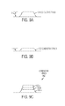
- FIGS. 9 a through 9 c illustrate exemplary stackups of conductive traces that can have border routing according to various embodiments.
- the thickness and material makeup of the conductive traces can be varied to meet the electrical requirements of the device.
- a single layer of conductive material having a thickness T can be used, for example, for shorter traces to match longer traces' resistance.
- a single layer of conductive material having a thickness t can be used, for example, for longer traces to reduce the traces' resistance.
- a single layer of material with higher resistivity can be used in some instances and a single layer of material with lower resistivity can be used in other instance.
- FIG. 9 a through 9 c illustrate exemplary stackups of conductive traces that can have border routing according to various embodiments.
- the thickness and material makeup of the conductive traces can be varied to meet the electrical requirements of the device.
- a single layer of conductive material having a thickness T can be used, for example, for shorter traces to match longer traces' resistance.
- Example trace materials include Molybdenum/Niobium (Mo/Nb), which has higher resistivity, and Aluminum/Neodymium (Al/Nd), which has lower resistivity.
- FIG. 10 illustrates exemplary mobile telephone 1000 that can include touch sensor panel 1024 and display device 1036 , the touch sensor panel and/or the display device including conductive traces formed in their border areas according to various embodiments.
- FIG. 11 illustrates exemplary digital media player 1100 that can include touch sensor panel 1124 and display device 1136 , the touch sensor panel and/or the display device including conductive traces formed in their border areas according to various embodiments.
- FIG. 12 illustrates exemplary personal computer 1200 that can include trackpad 1224 and display 1236 , the trackpad and/or the display including conductive traces formed in their border areas according to various embodiments.
- the mobile telephone, media player, and personal computer of FIGS. 10 through 12 can be more compact and have improved performance with conductive trace border routing according to various embodiments.
Abstract
Description
Claims (25)
Priority Applications (2)
| Application Number | Priority Date | Filing Date | Title |
|---|---|---|---|
| US13/007,493 US9491852B2 (en) | 2010-10-15 | 2011-01-14 | Trace border routing |
| US15/273,110 US9781823B2 (en) | 2010-10-15 | 2016-09-22 | Trace border routing |
Applications Claiming Priority (2)
| Application Number | Priority Date | Filing Date | Title |
|---|---|---|---|
| US39381810P | 2010-10-15 | 2010-10-15 | |
| US13/007,493 US9491852B2 (en) | 2010-10-15 | 2011-01-14 | Trace border routing |
Related Child Applications (1)
| Application Number | Title | Priority Date | Filing Date |
|---|---|---|---|
| US15/273,110 Continuation US9781823B2 (en) | 2010-10-15 | 2016-09-22 | Trace border routing |
Publications (2)
| Publication Number | Publication Date |
|---|---|
| US20120092273A1 US20120092273A1 (en) | 2012-04-19 |
| US9491852B2 true US9491852B2 (en) | 2016-11-08 |
Family
ID=45933723
Family Applications (2)
| Application Number | Title | Priority Date | Filing Date |
|---|---|---|---|
| US13/007,493 Active 2032-09-17 US9491852B2 (en) | 2010-10-15 | 2011-01-14 | Trace border routing |
| US15/273,110 Active US9781823B2 (en) | 2010-10-15 | 2016-09-22 | Trace border routing |
Family Applications After (1)
| Application Number | Title | Priority Date | Filing Date |
|---|---|---|---|
| US15/273,110 Active US9781823B2 (en) | 2010-10-15 | 2016-09-22 | Trace border routing |
Country Status (1)
| Country | Link |
|---|---|
| US (2) | US9491852B2 (en) |
Cited By (4)
| Publication number | Priority date | Publication date | Assignee | Title |
|---|---|---|---|---|
| US20150160769A1 (en) * | 2009-09-30 | 2015-06-11 | Apple Inc. | Touch screen border regions |
| US20170097703A1 (en) * | 2015-10-05 | 2017-04-06 | G2Touch Co., Ltd | Touch screen panel |
| US10048819B2 (en) | 2008-06-06 | 2018-08-14 | Apple Inc. | High resistivity metal fan out |
| US11334207B2 (en) | 2020-07-30 | 2022-05-17 | Samsung Display Co., Ltd. | Input sensing panel and an electronic apparatus having the same |
Families Citing this family (17)
| Publication number | Priority date | Publication date | Assignee | Title |
|---|---|---|---|---|
| US8749496B2 (en) | 2008-12-05 | 2014-06-10 | Apple Inc. | Integrated touch panel for a TFT display |
| KR20120092365A (en) * | 2011-02-11 | 2012-08-21 | 삼성전자주식회사 | Electrostatic capacity type touch screen panel display device |
| US8804347B2 (en) * | 2011-09-09 | 2014-08-12 | Apple Inc. | Reducing the border area of a device |
| KR101994971B1 (en) | 2012-05-16 | 2019-07-02 | 삼성디스플레이 주식회사 | Display device |
| US9395583B2 (en) | 2012-06-06 | 2016-07-19 | Apple Inc. | Column spacer design for a display incorporating a third metal layer |
| WO2015160377A1 (en) | 2014-04-16 | 2015-10-22 | Wrostix Technologies Llc | Structure for pixelated self-capacitance |
| US9984029B2 (en) * | 2014-04-18 | 2018-05-29 | Qualcomm Incorporated | Variable interconnect pitch for improved performance |
| US9367188B2 (en) | 2014-05-23 | 2016-06-14 | Apple Inc. | RC matching in a touch screen |
| WO2015183334A1 (en) * | 2014-05-28 | 2015-12-03 | Pylemta Management Llc | Narrow border touch screen |
| KR101597522B1 (en) * | 2014-08-28 | 2016-02-25 | 주식회사 지2터치 | The Touch Panel To Minimize Signal Distortion And, Display Apparatus Including The Same |
| US20160070394A1 (en) * | 2014-09-09 | 2016-03-10 | Uni-Pixel Displays, Inc. | Bezel circuit |
| CN104698711B (en) * | 2015-04-01 | 2018-06-01 | 上海天马微电子有限公司 | A kind of array substrate, display panel and electronic equipment |
| CN105045452B (en) * | 2015-08-19 | 2018-01-30 | 深圳市华星光电技术有限公司 | One kind touches display device and its array base palte |
| KR101904969B1 (en) | 2016-07-29 | 2018-10-10 | 삼성디스플레이 주식회사 | Display device |
| KR102436563B1 (en) * | 2017-12-27 | 2022-08-26 | 엘지디스플레이 주식회사 | Display Device |
| KR102611382B1 (en) | 2018-09-19 | 2023-12-07 | 삼성디스플레이 주식회사 | Touch sensing unit and display device including the same |
| CN113552970B (en) * | 2021-08-03 | 2024-03-15 | 京东方科技集团股份有限公司 | Display substrate and display device |
Citations (65)
| Publication number | Priority date | Publication date | Assignee | Title |
|---|---|---|---|---|
| US3773989A (en) | 1970-11-26 | 1973-11-20 | Plessey Handel Investment Ag | Touch-wire overlay masks for cathode ray tubes |
| JPH0315433U (en) | 1989-06-27 | 1991-02-15 | ||
| US5062916A (en) | 1990-08-01 | 1991-11-05 | W. H. Brady Co. | Method for the manufacture of electrical membrane panels having circuits on flexible plastic films |
| US5239152A (en) | 1990-10-30 | 1993-08-24 | Donnelly Corporation | Touch sensor panel with hidden graphic mode |
| US5483261A (en) | 1992-02-14 | 1996-01-09 | Itu Research, Inc. | Graphical input controller and method with rear screen image detection |
| US5488204A (en) | 1992-06-08 | 1996-01-30 | Synaptics, Incorporated | Paintbrush stylus for capacitive touch sensor pad |
| WO1996018179A1 (en) | 1994-12-07 | 1996-06-13 | Cirque Corporation | Capacitance-based proximity sensors with interference rejection apparatus and methods |
| US5825352A (en) | 1996-01-04 | 1998-10-20 | Logitech, Inc. | Multiple fingers contact sensing method for emulating mouse buttons and mouse operations on a touch sensor pad |
| US5835079A (en) | 1996-06-13 | 1998-11-10 | International Business Machines Corporation | Virtual pointing device for touchscreens |
| US5869791A (en) | 1995-04-18 | 1999-02-09 | U.S. Philips Corporation | Method and apparatus for a touch sensing device having a thin film insulation layer about the periphery of each sensing element |
| US5880411A (en) | 1992-06-08 | 1999-03-09 | Synaptics, Incorporated | Object position detector with edge motion feature and gesture recognition |
| US5994766A (en) * | 1998-09-21 | 1999-11-30 | Vlsi Technology, Inc. | Flip chip circuit arrangement with redistribution layer that minimizes crosstalk |
| JP2000163031A (en) | 1998-11-25 | 2000-06-16 | Seiko Epson Corp | Portable information equipment and information storage medium |
| US6188391B1 (en) | 1998-07-09 | 2001-02-13 | Synaptics, Inc. | Two-layer capacitive touchpad and method of making same |
| US6297811B1 (en) | 1999-06-02 | 2001-10-02 | Elo Touchsystems, Inc. | Projective capacitive touchscreen |
| US6310610B1 (en) | 1997-12-04 | 2001-10-30 | Nortel Networks Limited | Intelligent touch display |
| US6323846B1 (en) | 1998-01-26 | 2001-11-27 | University Of Delaware | Method and apparatus for integrating manual input |
| KR20020011716A (en) | 2000-08-04 | 2002-02-09 | 한승국 | Touch panel fabrication based on plating technology |
| JP2002342033A (en) | 2001-05-21 | 2002-11-29 | Sony Corp | Non-contact type user input device |
| US20030134095A1 (en) | 2002-01-16 | 2003-07-17 | Bottari Frank J | Method of applying an edge electrode pattern to a touch screen |
| US6690387B2 (en) | 2001-12-28 | 2004-02-10 | Koninklijke Philips Electronics N.V. | Touch-screen image scrolling system and method |
| JP2004296297A (en) | 2003-03-27 | 2004-10-21 | Optrex Corp | Manufacturing method of wiring board for organic el display device and organic el display device |
| US20050126831A1 (en) | 2003-12-15 | 2005-06-16 | Richter Paul J. | Wiring harness and touch sensor incorporating same |
| WO2005073791A1 (en) | 2004-01-05 | 2005-08-11 | Koninklijke Philips Electronics N.V. | Electronic device with bending wiring pattern |
| WO2005114369A2 (en) | 2004-05-06 | 2005-12-01 | Apple Computer, Inc. | Multipoint touchscreen |
| US20060026521A1 (en) | 2004-07-30 | 2006-02-02 | Apple Computer, Inc. | Gestures for touch sensitive input devices |
| US7015894B2 (en) | 2001-09-28 | 2006-03-21 | Ricoh Company, Ltd. | Information input and output system, method, storage medium, and carrier wave |
| US20060087379A1 (en) | 2004-10-21 | 2006-04-27 | International Business Machines Corporation | Method and structure to control common mode impedance in fan-out regions |
| US7075505B2 (en) * | 1999-12-10 | 2006-07-11 | Au Optronics Corporation | Liquid crystal display device, liquid crystal controller and video signal transmission method |
| US20060189123A1 (en) | 2003-09-04 | 2006-08-24 | Advanced Display Inc. | Etchant and method of etching |
| US20060197753A1 (en) | 2005-03-04 | 2006-09-07 | Hotelling Steven P | Multi-functional hand-held device |
| US7117464B2 (en) * | 2003-02-19 | 2006-10-03 | Hewlett-Packard Development Company, L.P. | System and method for evaluating signal coupling between differential traces in a package design |
| WO2007008518A2 (en) | 2005-07-07 | 2007-01-18 | 3M Innovative Properties Company | Touch panel sensor |
| US20070115263A1 (en) * | 2001-06-06 | 2007-05-24 | Brian Taylor | System for disposing a proximity sensitive touchpad behind a mobile phone keymat |
| US20070120471A1 (en) | 2003-11-14 | 2007-05-31 | Semiconductor Energy Laboratory Co., Ltd. | Display device and method for fabricating the same |
| US20070222763A1 (en) | 2006-03-22 | 2007-09-27 | Eastman Kodak Company | Increasing conductive polymer life by reversing voltage |
| US20070271399A1 (en) | 2006-05-18 | 2007-11-22 | Cypress Semiconductor Corporation | Tapered capsense structure |
| JP2008009920A (en) | 2006-06-30 | 2008-01-17 | Optrex Corp | Input device and manufacturing method therefor |
| US7321362B2 (en) | 2001-02-01 | 2008-01-22 | 3M Innovative Properties Company | Touch screen panel with integral wiring traces |
| CN101162418A (en) | 2006-10-11 | 2008-04-16 | 星电株式会社 | Touch panel input device |
| US20080117182A1 (en) | 2006-11-17 | 2008-05-22 | Samsung Electronics Co., Ltd. | Display device including sensing elements and driving method thereof |
| US20080143683A1 (en) | 2006-12-15 | 2008-06-19 | Apple Inc. | Pet-based touch pad |
| US20080158181A1 (en) | 2007-01-03 | 2008-07-03 | Apple Computer, Inc. | Double-sided touch sensitive panel and flex circuit bonding |
| US20080165158A1 (en) | 2007-01-05 | 2008-07-10 | Apple Inc. | Touch screen stack-ups |
| US7423621B2 (en) * | 2002-06-25 | 2008-09-09 | Chi Mei Optoelectronics Corporation | Driving circuit of a liquid crystal display device |
| US20080309633A1 (en) | 2007-06-13 | 2008-12-18 | Apple Inc. | Touch-sensitive display |
| US20090091551A1 (en) | 2007-10-04 | 2009-04-09 | Apple Inc. | Single-layer touch-sensitive display |
| US20090107736A1 (en) | 2007-10-30 | 2009-04-30 | N-Trig Ltd. | Laminated digitizer sensor |
| US20090143141A1 (en) | 2002-08-06 | 2009-06-04 | Igt | Intelligent Multiplayer Gaming System With Multi-Touch Display |
| US20090153509A1 (en) | 2007-12-14 | 2009-06-18 | Tsinghua University | Touch panel and display device using the same |
| US20090219258A1 (en) | 2008-08-01 | 2009-09-03 | 3M Innovative Properties Company | Touch screen sensor with low visibility conductors |
| US20090266621A1 (en) | 2008-04-25 | 2009-10-29 | Apple Inc. | Reliability Metal Traces |
| WO2009149014A1 (en) | 2008-06-06 | 2009-12-10 | Apple Inc. | High resistivity metal fan out |
| US20090314621A1 (en) | 2008-04-25 | 2009-12-24 | Apple Inc. | Brick Layout and Stackup for a Touch Screen |
| US20100013800A1 (en) | 2008-07-15 | 2010-01-21 | Elias John G | Capacitive Sensor Coupling Correction |
| US20100079384A1 (en) | 2008-09-26 | 2010-04-01 | Cypress Semiconductor Corporation | Capacitance touch screen |
| US7705952B2 (en) * | 2006-02-21 | 2010-04-27 | Au Optronics Corporation | Electronic device with uniform-resistance fan-out blocks |
| US20100166287A1 (en) | 2006-07-13 | 2010-07-01 | Cellomics, Inc. | Neuronal Profiling |
| US7755176B1 (en) | 2005-04-21 | 2010-07-13 | Amkor Technology, Inc. | Die-mounting substrate and method incorporating dummy traces for improving mounting film planarity |
| US20110074705A1 (en) * | 2009-09-30 | 2011-03-31 | Marduke Yousefpor | Touch Screen Border Regions |
| US20110163764A1 (en) | 2001-07-09 | 2011-07-07 | Uusi, Llc | Anti-entrapment system |
| US20110298731A1 (en) * | 2010-06-03 | 2011-12-08 | Chien-Hao Fu | Touch display device and touch display substrate thereof |
| US8179353B2 (en) * | 2000-02-18 | 2012-05-15 | Hitachi Displays, Ltd. | Driving method for display device |
| US8255830B2 (en) * | 2009-03-16 | 2012-08-28 | Apple Inc. | Methods and graphical user interfaces for editing on a multifunction device with a touch screen display |
| US20130038572A1 (en) | 2008-02-28 | 2013-02-14 | 3M Innovation Properties Company | Touch screen sensor having varying sheet resistance |
Family Cites Families (4)
| Publication number | Priority date | Publication date | Assignee | Title |
|---|---|---|---|---|
| JPH0315433A (en) | 1989-06-13 | 1991-01-23 | Canon Inc | Eye refractometer |
| TW293093B (en) * | 1994-09-08 | 1996-12-11 | Hitachi Ltd | |
| JPH1063198A (en) * | 1996-08-19 | 1998-03-06 | Denso Corp | Matrix type el display device |
| CN100530065C (en) | 2006-04-20 | 2009-08-19 | 铼宝科技股份有限公司 | Transparent touch-control panel structure |
-
2011
- 2011-01-14 US US13/007,493 patent/US9491852B2/en active Active
-
2016
- 2016-09-22 US US15/273,110 patent/US9781823B2/en active Active
Patent Citations (76)
| Publication number | Priority date | Publication date | Assignee | Title |
|---|---|---|---|---|
| US3773989A (en) | 1970-11-26 | 1973-11-20 | Plessey Handel Investment Ag | Touch-wire overlay masks for cathode ray tubes |
| JPH0315433U (en) | 1989-06-27 | 1991-02-15 | ||
| US5062916A (en) | 1990-08-01 | 1991-11-05 | W. H. Brady Co. | Method for the manufacture of electrical membrane panels having circuits on flexible plastic films |
| US5239152A (en) | 1990-10-30 | 1993-08-24 | Donnelly Corporation | Touch sensor panel with hidden graphic mode |
| US5483261A (en) | 1992-02-14 | 1996-01-09 | Itu Research, Inc. | Graphical input controller and method with rear screen image detection |
| US5880411A (en) | 1992-06-08 | 1999-03-09 | Synaptics, Incorporated | Object position detector with edge motion feature and gesture recognition |
| US5488204A (en) | 1992-06-08 | 1996-01-30 | Synaptics, Incorporated | Paintbrush stylus for capacitive touch sensor pad |
| WO1996018179A1 (en) | 1994-12-07 | 1996-06-13 | Cirque Corporation | Capacitance-based proximity sensors with interference rejection apparatus and methods |
| US5869791A (en) | 1995-04-18 | 1999-02-09 | U.S. Philips Corporation | Method and apparatus for a touch sensing device having a thin film insulation layer about the periphery of each sensing element |
| US5825352A (en) | 1996-01-04 | 1998-10-20 | Logitech, Inc. | Multiple fingers contact sensing method for emulating mouse buttons and mouse operations on a touch sensor pad |
| US5835079A (en) | 1996-06-13 | 1998-11-10 | International Business Machines Corporation | Virtual pointing device for touchscreens |
| US6310610B1 (en) | 1997-12-04 | 2001-10-30 | Nortel Networks Limited | Intelligent touch display |
| US6323846B1 (en) | 1998-01-26 | 2001-11-27 | University Of Delaware | Method and apparatus for integrating manual input |
| US6188391B1 (en) | 1998-07-09 | 2001-02-13 | Synaptics, Inc. | Two-layer capacitive touchpad and method of making same |
| US5994766A (en) * | 1998-09-21 | 1999-11-30 | Vlsi Technology, Inc. | Flip chip circuit arrangement with redistribution layer that minimizes crosstalk |
| JP2000163031A (en) | 1998-11-25 | 2000-06-16 | Seiko Epson Corp | Portable information equipment and information storage medium |
| US6297811B1 (en) | 1999-06-02 | 2001-10-02 | Elo Touchsystems, Inc. | Projective capacitive touchscreen |
| US20040149377A1 (en) | 1999-07-30 | 2004-08-05 | 3M Touch Systems, Inc. | Method of applying an edge electrode pattern to a touch screen |
| US7075505B2 (en) * | 1999-12-10 | 2006-07-11 | Au Optronics Corporation | Liquid crystal display device, liquid crystal controller and video signal transmission method |
| US8179353B2 (en) * | 2000-02-18 | 2012-05-15 | Hitachi Displays, Ltd. | Driving method for display device |
| KR20020011716A (en) | 2000-08-04 | 2002-02-09 | 한승국 | Touch panel fabrication based on plating technology |
| US7321362B2 (en) | 2001-02-01 | 2008-01-22 | 3M Innovative Properties Company | Touch screen panel with integral wiring traces |
| JP2002342033A (en) | 2001-05-21 | 2002-11-29 | Sony Corp | Non-contact type user input device |
| US20070115263A1 (en) * | 2001-06-06 | 2007-05-24 | Brian Taylor | System for disposing a proximity sensitive touchpad behind a mobile phone keymat |
| US20110163764A1 (en) | 2001-07-09 | 2011-07-07 | Uusi, Llc | Anti-entrapment system |
| US7015894B2 (en) | 2001-09-28 | 2006-03-21 | Ricoh Company, Ltd. | Information input and output system, method, storage medium, and carrier wave |
| US7184064B2 (en) | 2001-12-28 | 2007-02-27 | Koninklijke Philips Electronics N.V. | Touch-screen image scrolling system and method |
| US6690387B2 (en) | 2001-12-28 | 2004-02-10 | Koninklijke Philips Electronics N.V. | Touch-screen image scrolling system and method |
| US20030134095A1 (en) | 2002-01-16 | 2003-07-17 | Bottari Frank J | Method of applying an edge electrode pattern to a touch screen |
| US7423621B2 (en) * | 2002-06-25 | 2008-09-09 | Chi Mei Optoelectronics Corporation | Driving circuit of a liquid crystal display device |
| US20090143141A1 (en) | 2002-08-06 | 2009-06-04 | Igt | Intelligent Multiplayer Gaming System With Multi-Touch Display |
| US7117464B2 (en) * | 2003-02-19 | 2006-10-03 | Hewlett-Packard Development Company, L.P. | System and method for evaluating signal coupling between differential traces in a package design |
| JP2004296297A (en) | 2003-03-27 | 2004-10-21 | Optrex Corp | Manufacturing method of wiring board for organic el display device and organic el display device |
| US20060189123A1 (en) | 2003-09-04 | 2006-08-24 | Advanced Display Inc. | Etchant and method of etching |
| US20070120471A1 (en) | 2003-11-14 | 2007-05-31 | Semiconductor Energy Laboratory Co., Ltd. | Display device and method for fabricating the same |
| US8194044B2 (en) | 2003-12-15 | 2012-06-05 | 3M Innovative Properties Company | Wiring harness and touch sensor incorporating same |
| US7339579B2 (en) | 2003-12-15 | 2008-03-04 | 3M Innovative Properties Company | Wiring harness and touch sensor incorporating same |
| US20050126831A1 (en) | 2003-12-15 | 2005-06-16 | Richter Paul J. | Wiring harness and touch sensor incorporating same |
| WO2005073791A1 (en) | 2004-01-05 | 2005-08-11 | Koninklijke Philips Electronics N.V. | Electronic device with bending wiring pattern |
| CN1902538A (en) | 2004-01-05 | 2007-01-24 | 皇家飞利浦电子股份有限公司 | Electronic device with bending wiring pattern |
| WO2005114369A2 (en) | 2004-05-06 | 2005-12-01 | Apple Computer, Inc. | Multipoint touchscreen |
| US7663607B2 (en) | 2004-05-06 | 2010-02-16 | Apple Inc. | Multipoint touchscreen |
| US8479122B2 (en) | 2004-07-30 | 2013-07-02 | Apple Inc. | Gestures for touch sensitive input devices |
| US20060026521A1 (en) | 2004-07-30 | 2006-02-02 | Apple Computer, Inc. | Gestures for touch sensitive input devices |
| US20060087379A1 (en) | 2004-10-21 | 2006-04-27 | International Business Machines Corporation | Method and structure to control common mode impedance in fan-out regions |
| US20060197753A1 (en) | 2005-03-04 | 2006-09-07 | Hotelling Steven P | Multi-functional hand-held device |
| US7755176B1 (en) | 2005-04-21 | 2010-07-13 | Amkor Technology, Inc. | Die-mounting substrate and method incorporating dummy traces for improving mounting film planarity |
| WO2007008518A2 (en) | 2005-07-07 | 2007-01-18 | 3M Innovative Properties Company | Touch panel sensor |
| US7705952B2 (en) * | 2006-02-21 | 2010-04-27 | Au Optronics Corporation | Electronic device with uniform-resistance fan-out blocks |
| US20070222763A1 (en) | 2006-03-22 | 2007-09-27 | Eastman Kodak Company | Increasing conductive polymer life by reversing voltage |
| US20070271399A1 (en) | 2006-05-18 | 2007-11-22 | Cypress Semiconductor Corporation | Tapered capsense structure |
| JP2008009920A (en) | 2006-06-30 | 2008-01-17 | Optrex Corp | Input device and manufacturing method therefor |
| US20100166287A1 (en) | 2006-07-13 | 2010-07-01 | Cellomics, Inc. | Neuronal Profiling |
| CN101162418A (en) | 2006-10-11 | 2008-04-16 | 星电株式会社 | Touch panel input device |
| US20080100592A1 (en) | 2006-10-11 | 2008-05-01 | Hosiden Corporation | Touch panel input device |
| US20080117182A1 (en) | 2006-11-17 | 2008-05-22 | Samsung Electronics Co., Ltd. | Display device including sensing elements and driving method thereof |
| US20080143683A1 (en) | 2006-12-15 | 2008-06-19 | Apple Inc. | Pet-based touch pad |
| US20080158181A1 (en) | 2007-01-03 | 2008-07-03 | Apple Computer, Inc. | Double-sided touch sensitive panel and flex circuit bonding |
| US20080165158A1 (en) | 2007-01-05 | 2008-07-10 | Apple Inc. | Touch screen stack-ups |
| US20080309633A1 (en) | 2007-06-13 | 2008-12-18 | Apple Inc. | Touch-sensitive display |
| US20090091551A1 (en) | 2007-10-04 | 2009-04-09 | Apple Inc. | Single-layer touch-sensitive display |
| US20090107736A1 (en) | 2007-10-30 | 2009-04-30 | N-Trig Ltd. | Laminated digitizer sensor |
| US20090153509A1 (en) | 2007-12-14 | 2009-06-18 | Tsinghua University | Touch panel and display device using the same |
| US20130038572A1 (en) | 2008-02-28 | 2013-02-14 | 3M Innovation Properties Company | Touch screen sensor having varying sheet resistance |
| US20090314621A1 (en) | 2008-04-25 | 2009-12-24 | Apple Inc. | Brick Layout and Stackup for a Touch Screen |
| US20090266621A1 (en) | 2008-04-25 | 2009-10-29 | Apple Inc. | Reliability Metal Traces |
| US20090303189A1 (en) * | 2008-06-06 | 2009-12-10 | Grunthaner Martin Paul | High Resistivity Metal Fan Out |
| WO2009149014A1 (en) | 2008-06-06 | 2009-12-10 | Apple Inc. | High resistivity metal fan out |
| US9069418B2 (en) | 2008-06-06 | 2015-06-30 | Apple Inc. | High resistivity metal fan out |
| US20140139763A1 (en) | 2008-06-06 | 2014-05-22 | Apple Inc. | High resistivity metal fan out |
| US20100013800A1 (en) | 2008-07-15 | 2010-01-21 | Elias John G | Capacitive Sensor Coupling Correction |
| US20090219258A1 (en) | 2008-08-01 | 2009-09-03 | 3M Innovative Properties Company | Touch screen sensor with low visibility conductors |
| US20100079384A1 (en) | 2008-09-26 | 2010-04-01 | Cypress Semiconductor Corporation | Capacitance touch screen |
| US8255830B2 (en) * | 2009-03-16 | 2012-08-28 | Apple Inc. | Methods and graphical user interfaces for editing on a multifunction device with a touch screen display |
| US20110074705A1 (en) * | 2009-09-30 | 2011-03-31 | Marduke Yousefpor | Touch Screen Border Regions |
| US20110298731A1 (en) * | 2010-06-03 | 2011-12-08 | Chien-Hao Fu | Touch display device and touch display substrate thereof |
Non-Patent Citations (18)
| Title |
|---|
| Chinese Search Report mailed May 6, 2015, for CN Patent Application No. 201210581912.3, filed Jun. 1, 2009, with English translation, four pages. |
| European Search Report mailed Apr. 19, 2012, for EP Patent Application No. 12158277.9, four pages. |
| European Search Report mailed Feb. 4, 2013, for EP Patent Application No. 12195666.8, five pages. |
| European Search Report mailed Oct. 28, 2014, for EP Patent Application No. 14168254.2, three pages. |
| Final Office Action mailed Apr. 19, 2012, for U.S. Appl. No. 12/135,038, filed Jun. 6, 2008, eight pages. |
| Final Office Action mailed Jan. 14, 2016, for U.S. Appl. No. 14/163,899, filed Jan. 24, 2014, 17 pages. |
| Final Office Action mailed Nov. 6, 2013, for U.S. Appl. No. 12/135,038, filed Jun. 6, 2008, 14 pages. |
| International Search Report mailed Jul. 23, 2009, for PCT Patent Application No. PCT/US2009/045843, filed Jun. 1, 2009, two pages. |
| Lee, S.K. et al. (Apr. 1985). "A Multi-Touch Three Dimensional Touch-Sensitive Tablet," Proceedings of CHI: ACM Conference on Human Factors in Computing Systems, pp. 21-25. |
| Non-Final Office Action mailed Jun. 19, 2013, for U.S. Appl. No. 12/135,038, filed Jun. 6, 2008, 9 pages. |
| Non-Final Office Action mailed May 6, 2015, for U.S. Appl. No. 14/163,899, filed Jan. 24, 2014, 14 pages. |
| Non-Final Office Action mailed Sep. 17, 2014, for U.S. Appl. No. 12/135,038, filed Jun. 6, 2008, seven pages. |
| Non-Final Office Action mailed Sep. 29, 2011, for U.S. Appl. No. 12/135,038, filed Jun. 6, 2008, seven pages. |
| Notice of Allowance mailed Aug. 12, 2016, for U.S. Appl. No. 14/163,899, filed Jan. 24, 2014, ten pages. |
| Notice of Allowance mailed Mar. 12, 2015, for U.S. Appl. No. 12/135,038, filed Jun. 6, 2008, ten pages. |
| Rubine, D.H. (Dec. 1991). "The Automatic Recognition of Gestures," CMU-CS-91-202, Submitted in Partial Fulfillment of the Requirements for the Degree of Doctor of Philosophy in Computer Science at Carnegie Mellon University, 285 pages. |
| Rubine, D.H. (May 1992). "Combining Gestures and Direct Manipulation," CHI '92, pp. 659-660. |
| Westerman, W. (Spring 1999). "Hand Tracking, Finger Identification, and Chordic Manipulation on a Multi-Touch Surface," A Dissertation Submitted to the Faculty of the University of Delaware in Partial Fulfillment of the Requirements for the Degree of Doctor of Philosophy in Electrical Engineering, 364 pages. |
Cited By (7)
| Publication number | Priority date | Publication date | Assignee | Title |
|---|---|---|---|---|
| US10048819B2 (en) | 2008-06-06 | 2018-08-14 | Apple Inc. | High resistivity metal fan out |
| US20150160769A1 (en) * | 2009-09-30 | 2015-06-11 | Apple Inc. | Touch screen border regions |
| US9864445B2 (en) * | 2009-09-30 | 2018-01-09 | Apple Inc. | Touch screen border regions |
| US20170097703A1 (en) * | 2015-10-05 | 2017-04-06 | G2Touch Co., Ltd | Touch screen panel |
| US9904429B2 (en) * | 2015-10-05 | 2018-02-27 | G2Touch Co., Ltd. | Touch screen panel |
| US11334207B2 (en) | 2020-07-30 | 2022-05-17 | Samsung Display Co., Ltd. | Input sensing panel and an electronic apparatus having the same |
| US11675469B2 (en) | 2020-07-30 | 2023-06-13 | Samsung Display Co., Ltd. | Input sensing panel and an electronic apparatus having the same |
Also Published As
| Publication number | Publication date |
|---|---|
| US9781823B2 (en) | 2017-10-03 |
| US20120092273A1 (en) | 2012-04-19 |
| US20170013707A1 (en) | 2017-01-12 |
Similar Documents
| Publication | Publication Date | Title |
|---|---|---|
| US9491852B2 (en) | Trace border routing | |
| US20210081077A1 (en) | Sense Electrode Design | |
| KR102081318B1 (en) | Touch sensor integrated type liquid crystal display device | |
| KR101563796B1 (en) | Flexible circuit routing | |
| JP5583187B2 (en) | Touch screen integrated display | |
| WO2017049674A1 (en) | In-cell touch liquid crystal panel and array substrate thereof | |
| US9864445B2 (en) | Touch screen border regions | |
| KR102033614B1 (en) | Touch sensor integrated type display device | |
| TWI509490B (en) | Display device having touch sensing function | |
| US8797290B2 (en) | Sense electrode spine interpolation | |
| KR101360782B1 (en) | Display device with integrated touch screen | |
| US10386668B2 (en) | Display device, input detection device and electronic apparatus | |
| KR102297204B1 (en) | Touch sensor | |
| KR102305463B1 (en) | Display device including touch sensor and driving method thereof | |
| KR20130024328A (en) | Electrostatic capacity type touch screen panel | |
| WO2022241857A1 (en) | Self-contained touch-control display panel and display apparatus | |
| US10353525B2 (en) | Capacitive touch sensor apparatus | |
| KR101800894B1 (en) | Touch screen panel | |
| KR102095241B1 (en) | Electrostatic capacity type touch screen panel | |
| KR102367291B1 (en) | Touch panel and image display device comprising the same | |
| CN115424556A (en) | Display panel and display device | |
| KR20220170056A (en) | Row-scan touch screen with reduced resistance variation | |
| KR20200029982A (en) | Display device | |
| CN113311966A (en) | Touch display panel | |
| CN112909064A (en) | Display panel and display device |
Legal Events
| Date | Code | Title | Description |
|---|---|---|---|
| AS | Assignment |
Owner name: APPLE INC., CALIFORNIA Free format text: ASSIGNMENT OF ASSIGNORS INTEREST;ASSIGNORS:LYON, BENJAMIN B.;CHANG, SHIH CHANG;GRUNTHANER, MARTIN PAUL;REEL/FRAME:025666/0360 Effective date: 20110114 |
|
| STCF | Information on status: patent grant |
Free format text: PATENTED CASE |
|
| FEPP | Fee payment procedure |
Free format text: PAYOR NUMBER ASSIGNED (ORIGINAL EVENT CODE: ASPN); ENTITY STATUS OF PATENT OWNER: LARGE ENTITY |
|
| MAFP | Maintenance fee payment |
Free format text: PAYMENT OF MAINTENANCE FEE, 4TH YEAR, LARGE ENTITY (ORIGINAL EVENT CODE: M1551); ENTITY STATUS OF PATENT OWNER: LARGE ENTITY Year of fee payment: 4 |