US9490792B2 - Pulse width modulation with effective high duty resolution - Google Patents
Pulse width modulation with effective high duty resolution Download PDFInfo
- Publication number
- US9490792B2 US9490792B2 US12/703,239 US70323910A US9490792B2 US 9490792 B2 US9490792 B2 US 9490792B2 US 70323910 A US70323910 A US 70323910A US 9490792 B2 US9490792 B2 US 9490792B2
- Authority
- US
- United States
- Prior art keywords
- pwm
- value
- duty
- cycle
- signal
- Prior art date
- Legal status (The legal status is an assumption and is not a legal conclusion. Google has not performed a legal analysis and makes no representation as to the accuracy of the status listed.)
- Expired - Fee Related, expires
Links
- 238000000034 method Methods 0.000 claims description 78
- 230000004044 response Effects 0.000 claims description 20
- 230000000977 initiatory effect Effects 0.000 claims description 3
- 238000013459 approach Methods 0.000 description 9
- 230000008859 change Effects 0.000 description 6
- 238000010586 diagram Methods 0.000 description 5
- 230000008569 process Effects 0.000 description 5
- 238000001514 detection method Methods 0.000 description 4
- XUIMIQQOPSSXEZ-UHFFFAOYSA-N Silicon Chemical compound [Si] XUIMIQQOPSSXEZ-UHFFFAOYSA-N 0.000 description 3
- 230000008901 benefit Effects 0.000 description 3
- 230000000694 effects Effects 0.000 description 3
- 229910052710 silicon Inorganic materials 0.000 description 3
- 239000010703 silicon Substances 0.000 description 3
- 238000009825 accumulation Methods 0.000 description 2
- 230000003139 buffering effect Effects 0.000 description 2
- 230000011664 signaling Effects 0.000 description 2
- 230000004913 activation Effects 0.000 description 1
- 239000000872 buffer Substances 0.000 description 1
- 230000015556 catabolic process Effects 0.000 description 1
- 230000001351 cycling effect Effects 0.000 description 1
- 238000006731 degradation reaction Methods 0.000 description 1
- 230000000593 degrading effect Effects 0.000 description 1
- 230000003111 delayed effect Effects 0.000 description 1
- 230000008713 feedback mechanism Effects 0.000 description 1
- 230000000630 rising effect Effects 0.000 description 1
- 230000003068 static effect Effects 0.000 description 1
- 230000001360 synchronised effect Effects 0.000 description 1
Images


Classifications
-
- H—ELECTRICITY
- H03—ELECTRONIC CIRCUITRY
- H03K—PULSE TECHNIQUE
- H03K7/00—Modulating pulses with a continuously-variable modulating signal
- H03K7/08—Duration or width modulation ; Duty cycle modulation
-
- H—ELECTRICITY
- H04—ELECTRIC COMMUNICATION TECHNIQUE
- H04N—PICTORIAL COMMUNICATION, e.g. TELEVISION
- H04N9/00—Details of colour television systems
- H04N9/12—Picture reproducers
- H04N9/31—Projection devices for colour picture display, e.g. using electronic spatial light modulators [ESLM]
- H04N9/3102—Projection devices for colour picture display, e.g. using electronic spatial light modulators [ESLM] using two-dimensional electronic spatial light modulators
- H04N9/312—Driving therefor
- H04N9/3123—Driving therefor using pulse width modulation
-
- H05B33/0818—
-
- H05B33/0845—
-
- H—ELECTRICITY
- H05—ELECTRIC TECHNIQUES NOT OTHERWISE PROVIDED FOR
- H05B—ELECTRIC HEATING; ELECTRIC LIGHT SOURCES NOT OTHERWISE PROVIDED FOR; CIRCUIT ARRANGEMENTS FOR ELECTRIC LIGHT SOURCES, IN GENERAL
- H05B45/00—Circuit arrangements for operating light-emitting diodes [LED]
- H05B45/10—Controlling the intensity of the light
-
- H—ELECTRICITY
- H05—ELECTRIC TECHNIQUES NOT OTHERWISE PROVIDED FOR
- H05B—ELECTRIC HEATING; ELECTRIC LIGHT SOURCES NOT OTHERWISE PROVIDED FOR; CIRCUIT ARRANGEMENTS FOR ELECTRIC LIGHT SOURCES, IN GENERAL
- H05B45/00—Circuit arrangements for operating light-emitting diodes [LED]
- H05B45/30—Driver circuits
- H05B45/37—Converter circuits
- H05B45/3725—Switched mode power supply [SMPS]
-
- H—ELECTRICITY
- H02—GENERATION; CONVERSION OR DISTRIBUTION OF ELECTRIC POWER
- H02M—APPARATUS FOR CONVERSION BETWEEN AC AND AC, BETWEEN AC AND DC, OR BETWEEN DC AND DC, AND FOR USE WITH MAINS OR SIMILAR POWER SUPPLY SYSTEMS; CONVERSION OF DC OR AC INPUT POWER INTO SURGE OUTPUT POWER; CONTROL OR REGULATION THEREOF
- H02M1/00—Details of apparatus for conversion
- H02M1/08—Circuits specially adapted for the generation of control voltages for semiconductor devices incorporated in static converters
- H02M1/084—Circuits specially adapted for the generation of control voltages for semiconductor devices incorporated in static converters using a control circuit common to several phases of a multi-phase system
-
- Y—GENERAL TAGGING OF NEW TECHNOLOGICAL DEVELOPMENTS; GENERAL TAGGING OF CROSS-SECTIONAL TECHNOLOGIES SPANNING OVER SEVERAL SECTIONS OF THE IPC; TECHNICAL SUBJECTS COVERED BY FORMER USPC CROSS-REFERENCE ART COLLECTIONS [XRACs] AND DIGESTS
- Y02—TECHNOLOGIES OR APPLICATIONS FOR MITIGATION OR ADAPTATION AGAINST CLIMATE CHANGE
- Y02B—CLIMATE CHANGE MITIGATION TECHNOLOGIES RELATED TO BUILDINGS, e.g. HOUSING, HOUSE APPLIANCES OR RELATED END-USER APPLICATIONS
- Y02B20/00—Energy efficient lighting technologies, e.g. halogen lamps or gas discharge lamps
- Y02B20/30—Semiconductor lamps, e.g. solid state lamps [SSL] light emitting diodes [LED] or organic LED [OLED]
-
- Y02B20/346—
Definitions
- the present disclosure relates generally to pulse width modulation (PWM) signaling and more particularly to controlling a duty of a PWM signal.
- PWM pulse width modulation
- Pulse width modulation (PWM) signals often are used in display systems for precise control of display backlights or display screens.
- PWM signal generators are implemented with increasingly higher duty resolutions.
- these higher resolutions coupled with the high PWM cycle frequencies needed to avoid detectable audible noise result in the use of high clocking frequencies that require considerable power and silicon area to implement.
- PWM signal generators implementing these high clocking frequencies suffer from increased electromagnetic interference, PWM duty accuracy degradation, and timing issues due to the constrained rising/fall times of the corresponding PWM signaling.
- FIG. 1 is a diagram illustrating a pulse width modulation (PWM) signal generator implementing a contiguous duty pattern technique for providing an improved effective duty resolution in accordance with at least one embodiment of the present invention.
- PWM pulse width modulation
- FIG. 2 is a flow diagram illustrating a method of operation of the PWM signal generator of FIG. 1 in accordance with at least one embodiment of the present invention.
- FIG. 3 is a flow diagram illustrating an alternative method of operation of the PWM signal generator of FIG. 1 in accordance with at least one embodiment of the present invention.
- FIG. 4A is a chart illustrating a conventional dithering technique for PWM duty control.
- FIG. 4B is a chart illustrating an example of a contiguous duty pattern technique in accordance with at least one embodiment of the present invention.
- FIG. 5 is a flow diagram illustrating a method for selectively implementing either direct duty control mode or a pattern duty control mode at the PWM signal generator of FIG. 1 in accordance with at least one embodiment of the present disclosure.
- FIG. 6 is a diagram illustrating an example light emitting diode (LED) system implementing the PWM signal generator of FIG. 1 in accordance with at least one embodiment of the present invention.
- LED light emitting diode
- FIGS. 1-6 illustrate a pulse width modulation (PWM) signal generator for generating an output PWM signal with an improved effective PWM duty (also commonly referred to as the “duty ratio” or “duty cycle”) resolution.
- the PWM signal generator receives an N-bit binary value representing the duty to be implemented for the output PWM signal.
- the PWM signal generator sets a value X to the M least significant bits (LSBs) of the N-bit value and sets a value Y to the N-M most significant bits (MSBs) of this N-bit value, where M can be a determined based on the value N and a maximum implementable frequency of a clock signal used to time the generation of each PWM cycle.
- LSBs least significant bits
- MSBs most significant bits
- the PWM signal generator generates a cycle window of 2 M PWM cycles in the output PWM signal, each PWM cycle of the cycle window having a duty of either Y or Y+1, whereby the number of PWM cycles in the cycle window having the duty Y+1 is based on the value X.
- the PWM signal generator can be implemented with a native duty resolution of N-M bits while achieving a higher effective resolution when the duty of the PWM cycles in the cycle window are averaged over the duration of the cycle window.
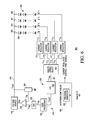
- FIG. 1 illustrates a PWM signal generator 100 in accordance with at least one embodiment of the present disclosure.
- the PWM signal generator 100 receives a PWM duty value 101 and generates a sequence of PWM cycles having a duty corresponding to the PWM duty value 101 for an output PWM signal 102 .
- the output PWM signal 102 then may be used to drive or otherwise control the operation of one or more PWM-driven components 104 .
- FIG. 1 illustrates a single output PWM signal 102 generated by the PWM signal generator 100 from the PWM duty value 101 for ease of illustration, any number of output PWM signals may be generated in parallel in accordance with the techniques described herein.
- the PWM-driven component 104 can include, for example, light emitting diodes (LEDs) of a LED-based display, a digital micromirror device, or an electronic motor.
- the PWM duty value 101 is provided by a PWM source 106 , which can include, for example, a video processing device or a graphics processor for a context whereby the PWM duty value 101 is used to control a backlight intensity or screen intensity of a display.
- the PWM source 106 can include a microcontroller for a context whereby the PWM duty value 101 is used to control a speed of a motor.
- the PWM signal generator 100 includes a controller 110 , a driver 112 , and a clock source 114 .
- the clock source 114 includes one or more oscillators, frequency dividers, or other clock generation circuits to generate a timing clock signal 116 .
- the timing clock signal 116 has a frequency f_res and is used to time the generation of the active portions of PWM cycles of the output PWM signal 102 .
- the clock source 114 generates a PWM cycle clock signal 118 that has a frequency f_pwm that represents the period or duration of each PWM cycle.
- the relationship between the frequency f_res and f_pwm is based on a programmable value M that controls the number of PWM cycles to be implemented in a cycle window.
- the driver 112 includes an input to receive a control signal 120 and an output to provide the output PWM signal 102 , whereby the driver 112 pulls the output PWM signal 102 to either a high reference voltage (e.g., Vdd or logic “1”) or to a low reference voltage (e.g., Vss or logic “0”) responsive to the state of the control signal 120 .
- a high reference voltage e.g., Vdd or logic “1”
- the controller 110 uses the timing clock signal 116 , the PWM duty value 101 , and the selected value M to control the state of the control signal 120 ; that is, to control the driver 112 in generating the output PWM signal 102 .
- the functionality of controller 110 can be implemented as an application specific integrated circuit (ASIC), one or more processors that execute software representative of the corresponding functionality, or a combination thereof.
- the controller can be implemented as discrete logic, an application specific integrated circuit (ASIC) device, a field programmable gate array (FPGA), and the like.
- the controller 110 includes a counter 122 , a signal timing module 124 , a window control module 126 , and a parameter control module 128 .
- the counter 122 includes an input to receive the timing clock signal 116 , an input to receive a reset signal 130 , and an output to provide a count value 132 , whereby the counter 122 adjusts the count value 132 for each clock cycle of the timing clock signal 116 , and whereby the counter 122 resets the count value 132 to a predetermined value, such as zero, in response to an assertion of the reset signal 130 .
- the adjustment to the count value 132 in response to the timing clock signal 116 can include incrementing or, alternatively, decrementing the count value 132 at the frequency f_res.
- the signal timing module 124 includes inputs to receive the count value 132 , a value P, a value D, and includes an output to provide the control signal 120 based on the relationship between the input values.
- the value D represents the duration, as measured by clock cycles of the timing clock signal 116 , of the active portion of a corresponding PWM cycle to be generated.
- the value P represents the duration, as measured by clock cycles of the timing clock signal 116 , of the period of the corresponding PWM cycle to be generated.
- the signal timing module 124 resets the counter 122 to initiate the next PWM cycle, accesses the value D from the window control module 126 , and then sets the state of the control signal 120 to a first state so as to direct the driver 112 to pull the output PWM signal 102 to the high reference voltage, thereby initiating the active portion of the PWM cycle.
- the signal timing module 124 sets the state of the control signal 120 to a second state so as to direct the driver 112 to pull the output PWM signal 102 to low voltage reference, thereby terminating the active portion of the PWM cycle.
- the PWM cycle clock signal 118 is used by the signal timing module 124 to time PWM cycle periods.
- the parameter control module 128 receives and buffers the PWM duty value 101 and the selected value M, which sets the number of PWM cycles to be implemented in a cycle window as 2 M PWM cycles per cycle window.
- the parameter control module 128 further has access to a value N that represents the native resolution of the PWM duty value 101 ; that is, the value N represents the number of bits in the PWM duty value 101 .
- the parameter control module 128 determines two non-negative integer values, X and Y, whereby the value X is set as the M least significant bits (LSBs) of the PWM duty value 101 and the value Y is set as the N-M most significant bits (MSBs) of the PWM duty value 101 .
- LSBs least significant bits
- MSBs most significant bits
- the values Y and Y+1 are used as measures of the duties (e.g., in terms of cycles of the timing clock signal 116 ) of respective PWM cycles of the cycle window and the value X is used as the measure of the number of PWM cycles in the cycle window that are to have the duty Y+1.
- the parameter control module 128 further provides the value P, which represents the period of the PWM cycles in the cycle window, to the signal timing module 124 for use in timing the period of each PWM cycle in the cycle window.
- the window control module 126 includes inputs to receive the values X, Y, and M from the parameter control module 128 , an input to receive the reset signal 130 , and an output to provide a select one of the value Y or the value Y+1 as the value D to the signal timing module 124 for use in setting the duty of a corresponding PWM cycle in the cycle window.
- the value X represents the number of PWM cycles in the cycle window that are to have the duty Y+1
- the value 2 M ⁇ X represents the number of PWM cycles in the cycle window that are to have the duty Y.
- the PWM cycles having the duty Y+1 are generated contiguously at the front, or beginning, of a cycle window.
- the PWM cycles having the duty Y+1 are generated contiguously together at the rear, or end, of a cycle window.
- the grouping of PWM cycles contiguously within a cycle window by duty so that the PWM cycles with the duty Y+1 occur at the front or rear of a cycle window can reduce the power consumed by the PWM signal generator 100 because only a single switch of the latch or latches storing the value D is needed for the single change between the duty Y and the duty Y+1 during a given cycle window.
- the particular one of the value Y or the value Y+1 that is provided as the value D depends on whether a number of PWM cycles having the duty Y+1 that already have been generated in the cycle window has reached the value X, which was determined from the M least-significant bits of the PWM duty value 101 .
- the window control module 126 sets a cycle count value n0 to the value X at the start of the cycle window and decrements n0 as each PWM cycle of the cycle window is completed, as indicated by a corresponding assertion of the reset signal 130 from the signal timing module 124 .
- the window control module 126 While the cycle count value n0 is greater than zero, the window control module 126 provides the value Y+1 as the value D, thereby causing the signal timing module 124 to generate a corresponding PWM cycle having the duty Y+1. Once the cycle count value n0 reaches zero during the cycle window, then the intended number of PWM cycles having the duty Y+1 have been generated for the cycle window (that is, X PWM cycles with the duty Y+1 have been created), and thus the window control module 126 switches to providing the value Y as the value D so that the remaining PWM cycles of the cycle window are generated with the duty Y.
- the window control module 126 sets the cycle count value n0 to the value 2 M ⁇ X at the start of the cycle window and decrements n0 as each PWM cycle of the cycle window is completed as indicated by a corresponding assertion of the reset signal 130 from the signal timing module 124 . While the cycle count value n0 is greater than zero, the window control module 126 provides the value Y as the value D, thereby causing the signal timing module 124 to generate a corresponding PWM cycle having the duty Y.
- the window control module 126 switches to providing the value Y+1 as the value D so that the remaining PWM cycles of the cycle window are generated with the duty Y+1.
- the PWM signal generator 100 can be used for PWM control in display systems, such as for generating the PWM signals used to control backlighting or display screens. In many display systems, it is advantageous to synchronize the PWM cycles of the PWM signals to the frame boundaries of the displayed video content.
- the PWM source 106 or another video component can provide a synchronization (SYNC) signal 134 , such as a vertical synchronization (VSYNC) signal that is representative of the frame boundaries in the corresponding displayed video content.
- the PWM signal generator 100 then may alter its operation in responsive to the frame boundaries so as to prematurely terminate a PWM cycle being generated therein and then initiate a new PWM cycle in response to the occurrence of a frame boundary.
- Updates to the PWM duty value may be implemented in accordance with at least three approaches.
- the consequence of the update that is, the corresponding change in the PWM output
- the SYNC signal 134 can be used to time the implementation of updates to the PWM duty value.
- the consequence of the update does not appear in the output PWM signal 102 until the SYNC signal 134 is asserted.
- an update to the PWM duty value 101 is implemented in the following PWM cycle, and an assertion of the SYNC signal 134 serves to terminate the current PWM cycle being generated and start a new PWM cycle.
- PWM duty updates occur on a PWM cycle basis, and the assertion of the SYNC signal 134 serves to trigger, in effect, a PWM cycle phase change.
- FIG. 2 illustrates an example method 200 of operation of the PWM signal generator 100 in accordance with at least one embodiment of the present disclosure.
- the controller 110 initializes in preparation for operation. This initialization process includes, for example, determining and setting the value M, which represents the number of PWM cycles to be implemented in a cycle window as 2 M PWM cycles and determining the value N, which represents the number of bits, or resolution, of the PWM duty value 101 .
- the values M and N can be hard-coded by a manufacturer or provider of the device implementing the PWM signal generator 100 .
- the value M can be programmable via, for example, a register or using a particular resistance at an external pin of the device.
- the value M is selected so as to meet two conditions.
- the first condition sets a minimum value for M based on the value N and a maximum implementable frequency of the timing clock signal 116 as dictated by, for example, budgeted silicon area, budgeted power consumption, or other design considerations.
- the second condition sets a maximum value for M so as to avoid visibly-detectable variation due to the resulting cycle window frequency.
- the parameter control module 128 or other component of the PWM signal generator 100 can determine a value for M that meets these two conditions by selecting a value for M that falls within a range determined based on calculations representing an expression:
- N represents the native resolution of the PWM signal generator 100 (that is, the number of bits in the PWM duty value 101 )
- f_res_max represents the maximum implementable frequency of the timing clock signal 116
- vis_thresh represents a minimum cycle window frequency (e.g., 50 Hz) above which variations due to changes within a cycle window are not expected to be detected by a typically viewer
- f_pwm represents the PWM cycle frequency, which can be represented either as the frequency of the PWM cycle clock signal 118 in the event that the PWM cycle clock signal 118 is used to time PWM cycles, or as f_res/P in the event that the value P is used to time PWM cycles.
- the initialization process further can include configuring a frequency divider, phase-locked loop, or other clocking circuit of the clock source 114 to generate the timing clock signal 116 so that the frequency f_res of the timing clock signal 116 is based on or otherwise related to the frequency f_pwm.
- the PWM source 106 provides a value PWM_DUTY[(N ⁇ 1):0] as the PWM duty value 101 to the controller 110 .
- the value D represents the duty of the next PWM cycle to be generated, whereby the value D is selectively set to either Y or Y+1.
- the value X represents the total number of PWM cycles of a cycle window that are to have the duty Y+1.
- n0 is initially set to the value X, n0 serves as a decrement counter used to count the number of PWM cycles with the duty Y+1 that have been generated in the current cycle window.
- the controller 110 is configured to generate the X PWM cycles having the duty Y+1 together as a contiguous group at the front of the cycle window. Accordingly, at block 208 the controller 110 compares the cycle count value n0 to 0.
- the controller 110 sets the value D to Y+1 so that the next PWM cycle to be generated has the duty Y+1. If n0 is not greater than 0, then X PWM cycles having the duty Y+1 have been generated for the cycle window and thus no further PWM cycles having the duty Y+1 are to be generated for the cycle window. In this instance, the controller 110 sets the value D to Y so that the next PWM cycle to be generated has the duty Y.
- the controller 110 controls the driver 112 so as to generate a PWM cycle having a duty represented by the value D (whereby D can be either Y or Y+1 depending on the corresponding iteration of block 208 ).
- the value D represents the duration of the active portion of the PWM cycle and the value P represents the period of the PWM cycle as measured in cycles of the timing clock signal 116 .
- the controller 110 can use the count value 132 of the counter 122 and the values P and D to time the generation of the PWM cycle so as to have a duty ratio of D:P.
- the controller 110 In response to the controller 110 determining at block 212 that generation of the PWM cycle has completed, at block 214 the controller 110 decrements the values n0 and n1 to reflect that another PWM cycle of the cycle window has completed. At block 216 , the controller 110 determines whether the cycle window has completed by comparing the cycle count value n1 to zero. If the controller 110 determines at block 216 that the cycle count value n1 has not yet reached zero and thus the cycle window has not completed, at block 218 the controller 110 determines whether X PWM cycles having the duty Y+1 have been generated for the cycle window by determining whether the cycle count value n0 is less than zero.
- the controller 110 can set the cycle count value n0 to zero at block 220 so that the value D is set to Y at the next iteration of block 208 for the remaining PWM cycles of the cycle window. Otherwise, if the cycle count value n0 is not less than zero, one or more PWM cycles having the duty Y+1 remain to be generated in the current cycle window and thus the controller 110 returns to block 208 without modifying the cycle count value n0 so that the value D is set to Y+1 at the next iteration of block 208 .
- the cycle window has completed and thus the operation of the controller 110 returns to the initialization process of block 206 for the next cycle window, which may use an updated value for PWM duty value 101 in the event that an update to the PWM duty value 101 occurred during generation of the previous cycle window.
- FIG. 3 illustrates an example method 300 of operation of the PWM signal generator 100 that is synchronized to frame boundaries or other frame synchronization events in accordance with at least one embodiment of the present disclosure.
- the method 300 includes two variations, identified as “Variation A” and “Variation B” in FIG. 3 , representing different example responses to frame boundaries represented by assertions of the SYNC signal 134 .
- the controller 110 initializes in preparation for operation in the manner described above with respect to block 202 .
- the PWM source 106 provides a value PWM_DUTY[(N ⁇ 1):0] as the PWM duty value 101 to the controller 110 .
- the controller 110 waits until the next frame boundary at block 308 , as indicated by an assertion of the SYNC signal 134 , and then begins generating the 2 M PWM cycles of the cycle window.
- the controller 110 initiates generation of the 2 M PWM cycles of the cycle window without waiting for next frame boundary.
- the controller 110 compares the cycle count value n0 to 0. If n0 is greater than 0, fewer than X PWM cycles having the duty Y+1 have been generated for the cycle window thus far. Accordingly, the controller 110 sets the value D to Y+1 so that the next PWM cycle to be generated has the duty Y+1. If n0 is not greater than 0, then X PWM cycles having the duty Y+1 have been generated for the cycle window and thus no further PWM cycles having the duty Y+1 are to be generated for the cycle window. In this instance, the controller 110 sets the value D to Y so that the next PWM cycle to be generated has the duty Y.
- the controller 110 accesses the current value for D and controls the driver 112 so as to generate a PWM cycle having a duty represented by the value D (whereby D can be either Y or Y+1 depending on the result of the corresponding iteration of block 310 ).
- the occurrence of a frame boundary causes the controller 110 to terminate the PWM cycle being generated and to start a new PWM cycle thereafter, thereby synchronizing the PWM cycles to the frame boundaries. Accordingly, while the PWM cycle is being generated at block 312 , the controller 110 monitors the SYNC signal 134 at block 314 to detect an occurrence of a frame boundary and terminates the PWM cycle being generated at block 316 in response to the frame boundary.
- method 300 identified as “Variation A” and by the lines from block 306 to block 310 and from block 316 to block 312 in FIG.
- updates to the PWM duty value 101 that occur during a cycle window are incorporated in the next PWM cycle of the cycle window by directly updating the values X and Y based on the new PWM duty value and updating n0 based on the new value X as the update to the PWM duty value 101 is received at block 306 and then proceeding back to block 310 .
- a PWM duty value change caused by a change to the PWM duty value 101 occurs on PWM cycle basis.
- An assertion of the SYNC signal 134 merely serves to start to the generation of the next PWM cycle, as represented by the flow from block 314 to block 316 and then block 312 .
- an update to the PWM output 120 caused by a change to the PWM duty value 101 happens only at a frame boundary. Accordingly, an update to the PWM duty value 101 occurring between frame boundaries is buffered until a frame boundary is detected at block 314 , at which point the values X and Y and the cycle count value n0 are updated based on the new PWM duty value 101 as described above at block 306 , and the method 300 then proceeds to block 310 .
- the approach of Variation B serves to delay the effect of an update to the PWM duty value 101 in the output PWM signal 102 until the next assertion of the SYNC signal 134 following the update.
- the controller 110 decrements the cycle count values n0 and n1 at block 320 to reflect that another PWM cycle of the cycle window has completed.
- the controller 110 determines whether the cycle window has completed by comparing the cycle count value n1 to zero. If the controller 110 determines at block 322 that the cycle count value n1 has not yet reached zero and thus the cycle window has not completed, at block 324 the controller 110 determines whether X PWM cycles having the duty Y+1 have been generated for the cycle window by determining whether the cycle count value n0 is less than zero.
- the controller 110 can set the cycle count value n0 to zero at block 326 so that the value D is set to Y at the next iteration of block 308 for the remaining PWM cycles of the cycle window. Otherwise, if the cycle count value n0 is not less than zero, one or more PWM cycles having the duty Y+1 remain to be generated in the current cycle window and thus the controller 110 returns to block 310 without modifying the cycle count value n0 so that the value D is set to Y+1 at the next iteration of block 310 .
- the controller 110 resets the cycle count value n1 to 2 M and resets the cycle count value n0 to X and begins the next cycle window by returning to block 310 .
- an update to the PWM duty value 101 can be directly implemented into a current cycle window or the update may be implemented only at a frame boundary.
- FIGS. 4A and 4B illustrates an example output of a conventional dithering technique for providing a higher-resolution duty control and an example output of the high-resolution duty control technique described above.
- the chart 401 of FIG. 4A illustrates an example operation of a conventional dithering technique described in, for example, U.S. Pat. No. 7,391,280 to generate sets 411 , 412 , 413 , 414 , and 415 of a series of sixteen PWM cycles for duties of 3488 (110110100000b), 3489 (110110100001b), 3490 (110110100010b), 3491 (110110100011b), and 3496 (110110101000b), respectively.
- the chart 402 of FIG. 4B illustrates an example implementation of the contiguous duty pattern technique described above to generate cycle windows 421 , 422 , 423 , 424 , and 425 of sixteen PWM cycles each for the same five duties.
- both the conventional dithering technique and the contiguous duty pattern technique described above implement a particular proportion of PWM cycles having a duty of 218 (Y) to PWM cycles having a duty of 219 (Y+1) to generate a desired average, or effective, PWM duty over the sixteen PWM cycle range.
- the conventional dithering technique relies on an accumulator and thus the PWM cycles having a duty of 219 are distributed among the sixteen PWM cycles based on the accumulation operation in a substantially non-contiguous manner.
- one embodiment of the technique described above provides that the PWM cycles having a duty of Y+1, or 219 in this example, are contiguously grouped together (for example, at the front or beginning of the cycle window or, alternatively, at the rear or end of the cycle window).
- the depicted cycle window 425 for the duty 3496 has eight PWM cycles having the duty 219 grouped contiguously at the front of the cycle window 425
- the set 415 for the same duty 3496 in the conventional dithering technique has the eight PWM cycles having the duty 219 non-contiguously distributed among the set at PWM cycles 2 , 4 , 6 , 8 , 10 , 12 , 14 , and 16 .
- the conventional dithering technique consumes more power due to the frequent context switches in latches and other buffering elements so as to achieve the frequent dithering between a duty of 218 and a duty of 219.
- the illustrated embodiment of an implementation of the high-resolution duty control technique requires only a single context switch between the duty Y and the duty Y+1 at a single point in any given cycle window.
- FIG. 5 illustrates an example method 500 for controlling a mode of PWM cycle generation for the PWM signal generator 100 of FIG. 1 in accordance with at least one embodiment of the present disclosure.
- the technique of generating a pattern of PWM cycles having duties that switch between Y and Y+1 permits an implementation of an effective duty resolution, when averaged over the cycle window, that is greater than the resolution of the duty value used as the basis for the duties Y and Y+1.
- Conventional dithering techniques also can provide higher resolution control, albeit at higher power consumption due to the frequent context switching as described above.
- the PWM signal generator 100 can selectively implement one of two modes depending on the PWM cycle frequency: a direct control mode whereby all N bits of the duty value are used to control the duty of the PWM cycles in the output PWM signal 102 ; and a pattern mode using either a conventional dithering technique or the contiguous pattern technique described above.
- the PWM signal generator 100 determines the PWM cycle frequency f_pwm of the output PWM signal 102 .
- the PWM cycle frequency f_pwm is determined from the frequency of the PWM cycle clock signal 118 .
- the PWM signal generator 100 uses the frequency f_pwm to determine whether to operate in the direct control mode or the pattern mode.
- the direct control mode can be implemented. Accordingly, at block 508 the PWM signal generator 100 is configured to the direct control mode so as to generate for the output PWM signal 102 one or more PWM cycles having a duty represented by all N bits of the PWM duty value 101 . For example, in the event that the PWM duty value 101 has a value 3490 , then the PWM signal generator 100 would generate one or more PWM cycles having the duty 3490 in the output PWM signal 102 .
- the direct control mode can be implemented in the methods 200 and 300 of operation of the PWM signal controller 100 illustrated in FIGS. 2 and 3 , respectively, by setting M to 0 at blocks 202 or 302 and setting n0 to 0 and n1 to 1 at blocks 206 or 306 and 328 .
- the PWM signal generator 100 instead can implement a duty pattern-based technique and use a timing clock signal with a frequency f_res that is lower in comparison to the direct control approach.
- the PWM signal generator 100 is configured to the pattern mode so as to generate for the output PWM signal 102 a series of PWM cycles, whereby the series includes a pattern of one or more PWM cycles having a duty Y and one or more PWM cycles having a duty Y+1, whereby the duty Y is based on a subset of the N bits of the PWM duty value 101 .
- the pattern implemented by the PWM signal generator 100 in this mode can include a contiguous pattern whereby the series of PWM cycles comprises the cycle window described above and the one or more PWM cycles having the duty Y+1 are contiguous within the series/cycle window in accordance with the above-described high-resolution control technique.
- the pattern implemented by the PWM signal generator 100 in this mode can include a conventional dithering pattern, such as, for example, the accumulation-based dithering approach described in U.S. Pat. No. 7,391,280.
- the value M is selected from the range defined by EQ. 1 above so as to satisfy the two conditions regarding the selection of a value for M.
- FIG. 6 illustrates an example implementation of the PWM signal generator 100 of FIG. 1 for dynamic power management in a light emitting diode (LED) system 600 having a plurality of LED strings.
- LED string refers to a grouping of one or more LEDs connected in series.
- the “head end” of a LED string is the end or portion of the LED string which receives the driving voltage/current and the “tail end” of the LED string is the opposite end or portion of the LED string.
- tail voltage refers the voltage at the tail end of a LED string or representation thereof (e.g., a voltage-divided representation, an amplified representation, etc.).
- subset of LED strings refers to one or more LED strings.
- the LED system 600 includes a LED panel 602 and a LED driver 604 .
- the LED panel 602 includes a plurality of LED strings (e.g., LED strings 605 , 606 , 607 , and 608 ).
- Each LED string includes one or more LEDs 609 connected in series.
- the LEDs 609 can include, for example, white LEDs, red, green, blue (RGB) LEDs, organic LEDs (OLEDs), etc.
- Each LED string is driven by the adjustable voltage V OUT received at the head end of the LED string from a voltage source 612 of the LED driver 604 via a voltage bus 610 (e.g., a conductive trace, wire, etc.).
- the voltage source 612 is implemented as a DC/DC converter configured to drive the output voltage V OUT using a supplied input voltage.
- the LED driver 604 includes a feedback controller 614 configured to control the voltage source 612 based on the tail voltages at the tail ends of the LED strings 605 - 608 .
- the LED driver 604 receives PWM duty values 601 (corresponding to the PWM duty value 101 of FIG. 1 ) that update or otherwise identifying the duty at which the LED strings 605 - 608 are to be driven, and the LED driver 604 is configured to activate the LED strings 605 - 608 based on the PWM duty value 601 .
- the feedback controller 614 includes a plurality of current regulators (e.g., current regulators 615 , 616 , 617 , and 618 ), an analog string select module 620 , an ADC 622 , a code processing module 624 , a control digital-to-analog converter (DAC) 626 , an error amplifier 628 , and a data/timing controller 630 .
- the data/timing controller 630 includes a PWM signal generator 632 (corresponding to the PWM signal generator 100 , FIG. 1 ).
- the current regulator 615 is configured to maintain the current I 1 flowing through the LED string 605 at or near a fixed current (e.g., 60 mA) when active.
- the current regulators 616 , 617 , and 618 are configured to maintain the currents I 2 , I 3 , and I 4 flowing through the LED strings 606 , 607 , and 608 , respectively, at or near the fixed current when active.
- a current regulator typically operates more effectively when the input of the current regulator is a non-zero voltage so as to accommodate the variation in the input voltage that often results from the current regulation process of the current regulator.
- This buffering voltage often is referred to as the “headroom” of the current regulator.
- the current regulators 615 - 618 are connected to the tail ends of the LED strings 605 - 608 , respectively, the tail voltages of the LED strings 605 - 608 represent the amounts of headroom available at the corresponding current regulators 615 - 618 .
- headroom in excess of that necessary for current regulation purposes results in unnecessary power consumption by the current regulator.
- the LED system 600 employs techniques to provide dynamic headroom control so as to maintain the minimum tail voltage of the active LED strings at or near a predetermined threshold voltage, thus maintaining the lowest headroom of the current regulators 615 - 618 at or near the predetermined threshold voltage.
- the threshold voltage can represent a determined balance between the need for sufficient headroom to permit proper current regulation by the current regulators 615 - 618 and the advantage of reduced power consumption by reducing the excess headroom at the current regulators 615 - 618 .
- the PWM signal generator 632 then generates a set of four output PWM signals in accordance with the techniques described above. Each output PWM signal is provided to a corresponding current regulator to control the activation of the corresponding LED strings.
- the analog string select module 620 includes a plurality of tail inputs coupled to the tail ends of the LED strings 605 - 608 to receive the tail voltages V T1 , V T2 , V T3 , and V T4 of the LED strings 605 - 608 , respectively, and an output to provide an analog signal 621 representative of the minimum tail voltage V Tmin of the LED strings 605 - 608 at any given point over a detection period.
- the analog string select module 620 is implemented as a diode-OR circuit having a plurality of inputs connected to the tail ends of the LED strings 605 - 608 and an output to provide the analog signal 621 .
- the ADC 622 is configured to generate one or more digital code values C OUT representative of the voltage of the analog signal 621 at one or more corresponding sample points.
- the code processing module 624 includes an input to receive the one or more code values C OUT and an output to provide a code value C reg based on the minimum value of the received code values C OUT for a given detection period or a previous value for C reg from a previous detection period.
- the code processing module 624 compares the code value C OUT to a threshold code value, C thresh , and generates a code value C reg based on the comparison.
- the code processing module 624 can be implemented as hardware, software executed by one or more processors, or a combination thereof. To illustrate, the code processing module 624 can be implemented as a logic-based hardware state machine, software executed by a processor, and the like.
- the control DAC 626 includes an input to receive the code value C reg and an output to provide a regulation voltage V reg representative of the code value C reg .
- the regulation voltage V reg is provided to the error amplifier 628 .
- the error amplifier 628 also receives a feedback voltage V fb representative of the output voltage V OUT .
- a voltage divider 640 is used to generate the voltage V fb from the output voltage V OUT .
- the error amplifier 628 compares the voltage V fb and the voltage V reg and configures a signal ADJ based on this comparison.
- the voltage source 612 receives the signal ADJ and adjusts the output voltage V OUT based on the magnitude of the signal ADJ.
- the LED driver 604 illustrated in FIG. 6 utilizes a feedback mechanism that permits the output voltage V OUT to be adjusted so as to reduce or minimize the power consumption of the LED driver 604 in the presence of variances in voltage drop across the LED strings 605 - 608 .
- a system comprises a pulse width modulation (PWM) signal generator to generate a PWM signal.
- the PWM signal generator comprises a parameter control module to receive a duty value having N bits and to determine a value X from the M least significant bits of the duty value and determine a value Y from the N-M most significant bits of the duty value, the values X and Y comprising non-negative integers.
- the PWM signal generator further comprises a signal timing module to sequentially generate 2M PWM cycles for a cycle window of the PWM signal based on the duty value, wherein for each PWM cycle of the cycle window the signal timing module is to access a value D and to generate an active portion of the PWM cycle based on the value D.
- the PWM signal generator further comprises a window control module to adjust a cycle count value as PWM cycles are completed and to switch the value D used by the signal timing module between the value Y and a value Y+1 based on a relationship between the cycle count value and a threshold value.
- the window control module initially sets the value D to the value Y+1 for the start of the cycle window and switches the value D to the value Y in response to the cycle count value reaching the threshold value.
- the window control module initially sets the value D to the value Y for the start of the cycle window and switches the value D to the value Y+1 in response to the cycle count value reaching the threshold value.
- the system further may comprise a display device having an input to receive the PWM signal.
- the signal timing module comprises a counter to increment a count value based on a clock signal, and the signal timing module times the active portion of each PWM cycle based on a relationship between the count value and the value D.
- the parameter control module is to determine a value for M based on N, a selected PWM cycle frequency, and a maximum implementable frequency for a clock signal used by the signal timing module to time the active portion of each PWM cycle of the cycle window.
- a method for generating a pulse width modulation (PWM) signal includes receiving, at a PWM signal generator, a duty value having N bits and determining whether a PWM cycle frequency of the PWM signal is above or below a threshold that is based on a maximum implementable frequency of a timing clock signal used to time generation of PWM cycles for the PWM signal.
- the method further includes, in response to determining the PWM cycle frequency is below the threshold, configuring the PWM signal generator to generate for the PWM signal one or more PWM cycles having a duty represented by all N bits of the duty value.
- the method also includes, in response to determining the PWM cycle frequency is not below the threshold, configuring the PWM signal generator to generate for the PWM signal a series of PWM cycles, whereby the series includes a pattern of one or more PWM cycles having a duty Y and one or more PWM cycles having a duty Y+1, the duty Y based on a subset of the N bits of the duty value.
- the pattern comprises a dithering pattern.
- the pattern comprises a contiguous pattern whereby the one or more PWM cycles having the duty Y+1 are contiguous in the series.
- a method for generating a PWM signal includes receiving, at a PWM signal generator, a duty value having N bits and determining a value X from the M least significant bits of the duty value and determine a value Y from the N-M most significant bits of the duty value, the values X and Y comprising non-negative integers.
- the method further includes sequentially generating 2M PWM cycles for a cycle window of the PWM signal based on the duty value, wherein for each PWM cycle of the cycle window the PWM signal generator accesses a value D and generates an active portion of the PWM cycle based on the value D.
- the method also includes adjusting a cycle count value as PWM cycles are completed, and switching the value D accessed by the PWM signal generator between the value Y and a value Y+1 based on a relationship between the cycle count value and a threshold value.
- the method also includes initially setting the value D to Y+1 for the start of the cycle window and wherein switching the value D comprises switching the value D to Y in response to the cycle count value reaching the threshold value.
- the method includes initially setting the value D to Y for the start of the cycle window, and wherein switching the value D comprises switching the value D to Y+1 in response to the cycle count value reaching the threshold value.
- the method further includes incrementing a count value based on a clock signal and timing the active portion of each PWM cycle based on a relationship between the value D and the count value.
- the method also includes determining a value for M based on N, a selected PWM cycle frequency, and a maximum implementable frequency for the first clock signal.
- the duty value comprises a first duty value and the method further comprises receiving, at the PWM signal generator, a second duty value having N bits during the generation of the PWM cycles for the cycle window, the second duty value to replace the first duty value.
- the method also includes determining, based on the second duty value, updated values for X and Y, implementing the updated values for X and Y for use in the generation of PWM cycles, and prematurely terminating a PWM cycle being generated at the occurrence of the frame boundary and initiating generation of a next PWM cycle.
- the duty value comprises a first duty value and the method further comprises receiving, at the PWM signal generator, a second duty value having N bits during the generation of the PWM cycles for the cycle window, the second duty value to replace the first duty value and determining, based on the second duty value, updated values for X and Y.
- the method further includes implementing the updated values for X and Y for use in the generation of PWM cycles and in response to an occurrence of a frame boundary during the cycle window, prematurely terminating a PWM cycle being generated at the occurrence of the frame boundary and starting generation of a next PWM cycle.
Abstract
Description
whereby N represents the native resolution of the PWM signal generator 100 (that is, the number of bits in the PWM duty value 101), f_res_max represents the maximum implementable frequency of the
Claims (20)
Priority Applications (1)
| Application Number | Priority Date | Filing Date | Title |
|---|---|---|---|
| US12/703,239 US9490792B2 (en) | 2010-02-10 | 2010-02-10 | Pulse width modulation with effective high duty resolution |
Applications Claiming Priority (1)
| Application Number | Priority Date | Filing Date | Title |
|---|---|---|---|
| US12/703,239 US9490792B2 (en) | 2010-02-10 | 2010-02-10 | Pulse width modulation with effective high duty resolution |
Publications (2)
| Publication Number | Publication Date |
|---|---|
| US20110193648A1 US20110193648A1 (en) | 2011-08-11 |
| US9490792B2 true US9490792B2 (en) | 2016-11-08 |
Family
ID=44353231
Family Applications (1)
| Application Number | Title | Priority Date | Filing Date |
|---|---|---|---|
| US12/703,239 Expired - Fee Related US9490792B2 (en) | 2010-02-10 | 2010-02-10 | Pulse width modulation with effective high duty resolution |
Country Status (1)
| Country | Link |
|---|---|
| US (1) | US9490792B2 (en) |
Cited By (3)
| Publication number | Priority date | Publication date | Assignee | Title |
|---|---|---|---|---|
| US20160233813A1 (en) * | 2015-02-09 | 2016-08-11 | Texas Instruments Incorporated | Increasing PWM Resolution for Digitally Controlled Motor Control Applications |
| US10226832B2 (en) * | 2013-06-24 | 2019-03-12 | Illinois Tool Works Inc. | Metal working power supply converter system and method |
| US10530343B2 (en) * | 2018-05-17 | 2020-01-07 | Hyundai Motor Company | System for monitoring operation execution of pulse width modulation duty for motor control |
Families Citing this family (10)
| Publication number | Priority date | Publication date | Assignee | Title |
|---|---|---|---|---|
| US9203305B2 (en) * | 2010-11-09 | 2015-12-01 | Zentrum Mikroelektronik Dresden Ag | Pulse width modulation power converter and control method employing different sets of PID coefficients |
| TWI569567B (en) * | 2010-11-09 | 2017-02-01 | Idt歐洲有限公司 | Method and for generating pwm signals |
| JP5977152B2 (en) * | 2012-11-20 | 2016-08-24 | 株式会社デンソー | Communication device |
| EP3105855B1 (en) | 2014-02-14 | 2018-05-09 | Philips Lighting Holding B.V. | Circuit and method for controlling pulse width modulation of a current supply for a load |
| US9818337B2 (en) * | 2014-07-24 | 2017-11-14 | Sct Technology, Ltd. | LED display control circuit with PWM circuit for driving a plurality of LED channels |
| US11874449B2 (en) | 2016-04-12 | 2024-01-16 | Jonathan Jacques | Pyramidal wall sections |
| US10263515B2 (en) | 2016-04-14 | 2019-04-16 | Licon Technology Corporation | Quasi-analog digital pulse-width modulation control |
| US10236866B2 (en) * | 2017-04-26 | 2019-03-19 | Infineon Technologies Ag | Pulse width modulation signal frequency generation |
| EP3965275A1 (en) * | 2020-09-08 | 2022-03-09 | Tridonic GmbH & Co. KG | Power factor correction circuit |
| CN112232525B (en) * | 2020-12-15 | 2021-07-13 | 鹏城实验室 | Driving mode characteristic construction and screening method and device and storage medium |
Citations (58)
| Publication number | Priority date | Publication date | Assignee | Title |
|---|---|---|---|---|
| US4162444A (en) | 1977-07-08 | 1979-07-24 | Tuscan Corporation | Peak level detector |
| US4615029A (en) | 1984-12-03 | 1986-09-30 | Texas Instruments Incorporated | Ring transmission network for interfacing control functions between master and slave devices |
| US4649432A (en) | 1984-01-27 | 1987-03-10 | Sony Corporation | Video display system |
| US4686640A (en) | 1984-12-12 | 1987-08-11 | Honeywell Inc. | Programmable digital hysteresis circuit |
| US4907862A (en) | 1985-03-05 | 1990-03-13 | Oy Lohja Ab | Method for generating elecronically controllable color elements and color display based on the method |
| US5025176A (en) | 1989-01-31 | 1991-06-18 | Fujitsu Limited | Peak level detection circuit |
| US5038055A (en) | 1988-12-02 | 1991-08-06 | Kabushiki Kaisha Toshiba | Peak level detecting device and method |
| US5508909A (en) | 1994-04-26 | 1996-04-16 | Patriot Sensors And Controls | Method and systems for use with an industrial controller |
| US5668611A (en) | 1994-12-21 | 1997-09-16 | Hughes Electronics | Full color sequential image projection system incorporating pulse rate modulated illumination |
| US5723950A (en) | 1996-06-10 | 1998-03-03 | Motorola | Pre-charge driver for light emitting devices and method |
| US5844540A (en) | 1994-05-31 | 1998-12-01 | Sharp Kabushiki Kaisha | Liquid crystal display with back-light control function |
| US5898329A (en) | 1996-12-31 | 1999-04-27 | Stmicroelectronics, Inc. | Programmable pulse width modulation circuit |
| US6281822B1 (en) | 1999-05-28 | 2001-08-28 | Dot Wireless, Inc. | Pulse density modulator with improved pulse distribution |
| US6369782B2 (en) * | 1997-04-26 | 2002-04-09 | Pioneer Electric Corporation | Method for driving a plasma display panel |
| US20030160804A1 (en) | 2002-02-22 | 2003-08-28 | Willis Thomas E. | Digitally driving pixels from pulse width modulated waveforms |
| US20030201986A1 (en) | 2002-04-30 | 2003-10-30 | Willis Thomas E. | Generating pulse width modulated waveforms to digitally drive pixels |
| JP2003332624A (en) | 2002-05-07 | 2003-11-21 | Rohm Co Ltd | Light emitting element drive device and electronic apparatus having light emitting element |
| US20040008159A1 (en) | 2002-07-10 | 2004-01-15 | Cunha John Da | Active display system and method with optical addressing |
| US20040233144A1 (en) | 2003-05-09 | 2004-11-25 | Rader William E. | Method and apparatus for driving leds |
| US20040232964A1 (en) | 2003-05-19 | 2004-11-25 | Texas Instruments Incorporated | Distributing clock and programming phase shift in multiphase parallelable converters |
| US20040251942A1 (en) | 2003-06-12 | 2004-12-16 | Delta Electronics, Inc. | PWM buffer circuit for adjusting a frequency and a duty cycle of a PWM signal |
| US6864641B2 (en) | 2003-02-20 | 2005-03-08 | Visteon Global Technologies, Inc. | Method and apparatus for controlling light emitting diodes |
| JP2005116199A (en) | 2003-10-03 | 2005-04-28 | Arueido Kk | Led lighting control device, and led lighting control method |
| US6937084B2 (en) | 2001-06-01 | 2005-08-30 | Microchip Technology Incorporated | Processor with dual-deadtime pulse width modulation generator |
| US6943500B2 (en) | 2001-10-19 | 2005-09-13 | Clare Micronix Integrated Systems, Inc. | Matrix element precharge voltage adjusting apparatus and method |
| US20050275355A1 (en) | 2004-06-10 | 2005-12-15 | Samuelsson Ulf R | Method and system for enhanced dimming resolution in a light ballast through use of multiple control frequencies |
| US6995592B2 (en) | 2003-11-06 | 2006-02-07 | Stmicroelectronics Pvt. Ltd. | Method and system for generating variable frequency cyclic waveforms using pulse width modulation |
| US20060064609A1 (en) | 2004-08-23 | 2006-03-23 | Microchip Technology Incorporated | Digital processor with pulse width modulation module having dynamically adjustable phase offset capability, high speed operation and simultaneous update of multiple pulse width modulation duty cycle registers |
| US20060164142A1 (en) * | 2005-01-21 | 2006-07-27 | Stanley Michael E | High resolution pulse width modulator |
| US20060186830A1 (en) | 2005-02-07 | 2006-08-24 | California Micro Devices | Automatic voltage selection for series driven LEDs |
| US7106294B2 (en) | 2002-03-28 | 2006-09-12 | Matsushita Electric Industrial Co., Ltd | Liquid crystal display device |
| US7126397B1 (en) | 2004-12-30 | 2006-10-24 | National Semiconductor Corporation | Pulse width modulation carrier frequency technique |
| US7176948B2 (en) | 2000-04-12 | 2007-02-13 | Honeywell International Inc. | Method, apparatus and computer program product for controlling LED backlights and for improved pulse width modulation resolution |
| US20070047272A1 (en) * | 2005-08-30 | 2007-03-01 | Microchip Technology Incorporated | Pulse width modulation frequency dithering in a switch mode power supply |
| US20070080911A1 (en) | 2005-10-11 | 2007-04-12 | Da Liu | Controller circuitry for light emitting diodes |
| US20070182701A1 (en) | 2006-02-06 | 2007-08-09 | Min-Gyu Kim | Method of driving a lamp, lamp driving apparatus, and liquid crystal display device having the same |
| US7262724B2 (en) | 2005-03-31 | 2007-08-28 | Freescale Semiconductor, Inc. | System and method for adjusting dynamic range of analog-to-digital converter |
| US20070253330A1 (en) | 2005-01-07 | 2007-11-01 | Yuji Tochio | Node setting apparatus, network system, node setting method, and computer product |
| US20080054815A1 (en) | 2006-09-01 | 2008-03-06 | Broadcom Corporation | Single inductor serial-parallel LED driver |
| US20080074381A1 (en) | 2004-07-13 | 2008-03-27 | Yasuhiro Kumamoto | Liquid Crystal Display and Its Light Source Driving Method |
| US7391280B2 (en) | 2004-02-17 | 2008-06-24 | Sunplus Technology Co., Ltd. | Circuit and method for pulse width modulation |
| WO2008124718A2 (en) | 2007-04-10 | 2008-10-16 | Lumination Llc | Light emitting diode controller, methods of light emitting diode control, and components for same |
| US20080297067A1 (en) | 2007-05-31 | 2008-12-04 | Texas Instruments Incorporated | Power regulation for led strings |
| US20090073735A1 (en) | 2007-09-13 | 2009-03-19 | Kesler Scott B | Analog duty cycle replicating frequency converter for pwm signals |
| US20090128045A1 (en) | 2007-11-16 | 2009-05-21 | Gregory Szczeszynski | Electronic Circuits for Driving Series Connected Light Emitting Diode Strings |
| US7550932B2 (en) | 2004-08-16 | 2009-06-23 | Richtek Technology Corp | Control method and device for a power-converting module that drives a light-emitting component |
| US20090187925A1 (en) | 2008-01-17 | 2009-07-23 | Delta Electronic Inc. | Driver that efficiently regulates current in a plurality of LED strings |
| US20090230874A1 (en) | 2008-03-12 | 2009-09-17 | Freescale Semiconductor, Inc. | Led driver with segmented dynamic headroom control |
| US20090230891A1 (en) | 2008-03-12 | 2009-09-17 | Freescale Semiconductor, Inc. | Led driver with dynamic power management |
| US7593243B2 (en) | 2006-10-09 | 2009-09-22 | Honeywell International Inc. | Intelligent method for DC bus voltage ripple compensation for power conversion units |
| US20090273288A1 (en) | 2008-03-12 | 2009-11-05 | Freescale Semiconductor, Inc. | Led driver with dynamic power management |
| US20090315481A1 (en) | 2008-06-23 | 2009-12-24 | Freescale Semiconductor, Inc. | Method and device for led channel managment in led driver |
| US20100026203A1 (en) | 2008-07-31 | 2010-02-04 | Freescale Semiconductor, Inc. | Led driver with frame-based dynamic power management |
| US20100085295A1 (en) | 2008-10-03 | 2010-04-08 | Freescale Semiconductor, Inc. | Frequency synthesis and synchronization for led drivers |
| US7741885B1 (en) | 2009-03-04 | 2010-06-22 | Yazaki North America | Frequency multiplier |
| US7800415B2 (en) | 2008-12-18 | 2010-09-21 | Silicon Laboratories, Inc. | Circuit device to produce an output signal including dither |
| US20110169679A1 (en) | 2008-11-28 | 2011-07-14 | Kohei Teramoto | Digital-to-analog converter |
| US8358264B2 (en) * | 2008-12-16 | 2013-01-22 | Renesas Electronics Corporation | Backlight brightness control for panel display device including controlling a brightness of the backlight to have a variable brightness in a portion of a period |
Family Cites Families (1)
| Publication number | Priority date | Publication date | Assignee | Title |
|---|---|---|---|---|
| EP1296492B1 (en) * | 2001-09-21 | 2006-02-15 | Alcatel | Multicarrier receiver with a sliding window Fourier transform and a Fourier transform |
-
2010
- 2010-02-10 US US12/703,239 patent/US9490792B2/en not_active Expired - Fee Related
Patent Citations (61)
| Publication number | Priority date | Publication date | Assignee | Title |
|---|---|---|---|---|
| US4162444A (en) | 1977-07-08 | 1979-07-24 | Tuscan Corporation | Peak level detector |
| US4649432A (en) | 1984-01-27 | 1987-03-10 | Sony Corporation | Video display system |
| US4615029A (en) | 1984-12-03 | 1986-09-30 | Texas Instruments Incorporated | Ring transmission network for interfacing control functions between master and slave devices |
| US4686640A (en) | 1984-12-12 | 1987-08-11 | Honeywell Inc. | Programmable digital hysteresis circuit |
| US4907862A (en) | 1985-03-05 | 1990-03-13 | Oy Lohja Ab | Method for generating elecronically controllable color elements and color display based on the method |
| US5038055A (en) | 1988-12-02 | 1991-08-06 | Kabushiki Kaisha Toshiba | Peak level detecting device and method |
| US5025176A (en) | 1989-01-31 | 1991-06-18 | Fujitsu Limited | Peak level detection circuit |
| US5508909A (en) | 1994-04-26 | 1996-04-16 | Patriot Sensors And Controls | Method and systems for use with an industrial controller |
| US5844540A (en) | 1994-05-31 | 1998-12-01 | Sharp Kabushiki Kaisha | Liquid crystal display with back-light control function |
| US5668611A (en) | 1994-12-21 | 1997-09-16 | Hughes Electronics | Full color sequential image projection system incorporating pulse rate modulated illumination |
| US5723950A (en) | 1996-06-10 | 1998-03-03 | Motorola | Pre-charge driver for light emitting devices and method |
| US5898329A (en) | 1996-12-31 | 1999-04-27 | Stmicroelectronics, Inc. | Programmable pulse width modulation circuit |
| US6369782B2 (en) * | 1997-04-26 | 2002-04-09 | Pioneer Electric Corporation | Method for driving a plasma display panel |
| US6281822B1 (en) | 1999-05-28 | 2001-08-28 | Dot Wireless, Inc. | Pulse density modulator with improved pulse distribution |
| US7176948B2 (en) | 2000-04-12 | 2007-02-13 | Honeywell International Inc. | Method, apparatus and computer program product for controlling LED backlights and for improved pulse width modulation resolution |
| US6937084B2 (en) | 2001-06-01 | 2005-08-30 | Microchip Technology Incorporated | Processor with dual-deadtime pulse width modulation generator |
| US6943500B2 (en) | 2001-10-19 | 2005-09-13 | Clare Micronix Integrated Systems, Inc. | Matrix element precharge voltage adjusting apparatus and method |
| US20030160804A1 (en) | 2002-02-22 | 2003-08-28 | Willis Thomas E. | Digitally driving pixels from pulse width modulated waveforms |
| US7106294B2 (en) | 2002-03-28 | 2006-09-12 | Matsushita Electric Industrial Co., Ltd | Liquid crystal display device |
| US20030201986A1 (en) | 2002-04-30 | 2003-10-30 | Willis Thomas E. | Generating pulse width modulated waveforms to digitally drive pixels |
| US20040208011A1 (en) | 2002-05-07 | 2004-10-21 | Sachito Horiuchi | Light emitting element drive device and electronic device having light emitting element |
| JP2003332624A (en) | 2002-05-07 | 2003-11-21 | Rohm Co Ltd | Light emitting element drive device and electronic apparatus having light emitting element |
| US20040008159A1 (en) | 2002-07-10 | 2004-01-15 | Cunha John Da | Active display system and method with optical addressing |
| US6864641B2 (en) | 2003-02-20 | 2005-03-08 | Visteon Global Technologies, Inc. | Method and apparatus for controlling light emitting diodes |
| US20040233144A1 (en) | 2003-05-09 | 2004-11-25 | Rader William E. | Method and apparatus for driving leds |
| US20040232964A1 (en) | 2003-05-19 | 2004-11-25 | Texas Instruments Incorporated | Distributing clock and programming phase shift in multiphase parallelable converters |
| US20040251942A1 (en) | 2003-06-12 | 2004-12-16 | Delta Electronics, Inc. | PWM buffer circuit for adjusting a frequency and a duty cycle of a PWM signal |
| JP2005116199A (en) | 2003-10-03 | 2005-04-28 | Arueido Kk | Led lighting control device, and led lighting control method |
| US7436378B2 (en) | 2003-10-03 | 2008-10-14 | Al-Aid Corporation | LED-switching controller and LED-switching control method |
| US6995592B2 (en) | 2003-11-06 | 2006-02-07 | Stmicroelectronics Pvt. Ltd. | Method and system for generating variable frequency cyclic waveforms using pulse width modulation |
| US7391280B2 (en) | 2004-02-17 | 2008-06-24 | Sunplus Technology Co., Ltd. | Circuit and method for pulse width modulation |
| US20050275355A1 (en) | 2004-06-10 | 2005-12-15 | Samuelsson Ulf R | Method and system for enhanced dimming resolution in a light ballast through use of multiple control frequencies |
| US20080074381A1 (en) | 2004-07-13 | 2008-03-27 | Yasuhiro Kumamoto | Liquid Crystal Display and Its Light Source Driving Method |
| US7550932B2 (en) | 2004-08-16 | 2009-06-23 | Richtek Technology Corp | Control method and device for a power-converting module that drives a light-emitting component |
| US20060064609A1 (en) | 2004-08-23 | 2006-03-23 | Microchip Technology Incorporated | Digital processor with pulse width modulation module having dynamically adjustable phase offset capability, high speed operation and simultaneous update of multiple pulse width modulation duty cycle registers |
| US7126397B1 (en) | 2004-12-30 | 2006-10-24 | National Semiconductor Corporation | Pulse width modulation carrier frequency technique |
| US20070253330A1 (en) | 2005-01-07 | 2007-11-01 | Yuji Tochio | Node setting apparatus, network system, node setting method, and computer product |
| US20060164142A1 (en) * | 2005-01-21 | 2006-07-27 | Stanley Michael E | High resolution pulse width modulator |
| US20060186830A1 (en) | 2005-02-07 | 2006-08-24 | California Micro Devices | Automatic voltage selection for series driven LEDs |
| US7262724B2 (en) | 2005-03-31 | 2007-08-28 | Freescale Semiconductor, Inc. | System and method for adjusting dynamic range of analog-to-digital converter |
| US20070047272A1 (en) * | 2005-08-30 | 2007-03-01 | Microchip Technology Incorporated | Pulse width modulation frequency dithering in a switch mode power supply |
| US20070080911A1 (en) | 2005-10-11 | 2007-04-12 | Da Liu | Controller circuitry for light emitting diodes |
| US20070182701A1 (en) | 2006-02-06 | 2007-08-09 | Min-Gyu Kim | Method of driving a lamp, lamp driving apparatus, and liquid crystal display device having the same |
| US20080054815A1 (en) | 2006-09-01 | 2008-03-06 | Broadcom Corporation | Single inductor serial-parallel LED driver |
| US7593243B2 (en) | 2006-10-09 | 2009-09-22 | Honeywell International Inc. | Intelligent method for DC bus voltage ripple compensation for power conversion units |
| WO2008124718A2 (en) | 2007-04-10 | 2008-10-16 | Lumination Llc | Light emitting diode controller, methods of light emitting diode control, and components for same |
| US20080297067A1 (en) | 2007-05-31 | 2008-12-04 | Texas Instruments Incorporated | Power regulation for led strings |
| US20090073735A1 (en) | 2007-09-13 | 2009-03-19 | Kesler Scott B | Analog duty cycle replicating frequency converter for pwm signals |
| US7511545B1 (en) | 2007-09-13 | 2009-03-31 | Delphi Technologies, Inc. | Analog duty cycle replicating frequency converter for PWM signals |
| US20090128045A1 (en) | 2007-11-16 | 2009-05-21 | Gregory Szczeszynski | Electronic Circuits for Driving Series Connected Light Emitting Diode Strings |
| US20090187925A1 (en) | 2008-01-17 | 2009-07-23 | Delta Electronic Inc. | Driver that efficiently regulates current in a plurality of LED strings |
| US20090230891A1 (en) | 2008-03-12 | 2009-09-17 | Freescale Semiconductor, Inc. | Led driver with dynamic power management |
| US20090230874A1 (en) | 2008-03-12 | 2009-09-17 | Freescale Semiconductor, Inc. | Led driver with segmented dynamic headroom control |
| US20090273288A1 (en) | 2008-03-12 | 2009-11-05 | Freescale Semiconductor, Inc. | Led driver with dynamic power management |
| US20090315481A1 (en) | 2008-06-23 | 2009-12-24 | Freescale Semiconductor, Inc. | Method and device for led channel managment in led driver |
| US20100026203A1 (en) | 2008-07-31 | 2010-02-04 | Freescale Semiconductor, Inc. | Led driver with frame-based dynamic power management |
| US20100085295A1 (en) | 2008-10-03 | 2010-04-08 | Freescale Semiconductor, Inc. | Frequency synthesis and synchronization for led drivers |
| US20110169679A1 (en) | 2008-11-28 | 2011-07-14 | Kohei Teramoto | Digital-to-analog converter |
| US8358264B2 (en) * | 2008-12-16 | 2013-01-22 | Renesas Electronics Corporation | Backlight brightness control for panel display device including controlling a brightness of the backlight to have a variable brightness in a portion of a period |
| US7800415B2 (en) | 2008-12-18 | 2010-09-21 | Silicon Laboratories, Inc. | Circuit device to produce an output signal including dither |
| US7741885B1 (en) | 2009-03-04 | 2010-06-22 | Yazaki North America | Frequency multiplier |
Non-Patent Citations (32)
| Title |
|---|
| Akira Takahashi, Electronic Products: "Methods and features of LED drivers," Mar. 2008, 3 pages. |
| Ex parte Quayle Action mailed May 31, 2013 for U.S. Appl. No. 13/025,201, 31 pages. |
| Feng et al., "A New Switched-Capacitor Frequency Modulated Driver for Light Emitting Diodes," Review of Scientific Instruments 78, 114710, American Institute of Physics, 2007, 4 pages. |
| International Application No. PCT/US2009/035284, Search Report and Written Opinion, Oct. 28, 2009, 11 pages. |
| Luke Huiyong Chung, Electronic Products: "Driver ICs for LED BLUs," May 1, 2008, 3 pages. |
| MAXIM: "Application Note 810, Understanding Flash ADCs," Oct. 2, 2001, 8 pages. |
| Mc Nerney, Tim, "constant-current power supply for Luxeon 5W LED with low-voltage warning and shut-off Software Documentation, as shipped to Mali in first 45 prototypes," Nov. 2004, www.designthatmatters.org/ke/pubs/kled-doc.txt, 5 pages. |
| National Semiconductor Data Sheet: "LM3432/LM3432B 6-Channel Current Regulator for LED Backlight Application," May 22, 2008, pp. 1-18. |
| Non-final Office Action mailed May 9, 2012 for U.S. Appl. No. 12/244,796, 36 pages. |
| Non-Final Office Action mailed Oct. 20, 2011 for U.S. Appl. No. 12/537,443, 22 pages. |
| Notice of Allowance dated Jul. 17, 2013 in U.S. Appl. No. 13/025,201. |
| Notice of Allowance dated Jul. 25, 2012 in U.S. Appl. No. 12/244,796. |
| Notice of Allowance dated Jun. 8, 2012 in U.S. Appl. No. 12/537,443. |
| Notice of Allowance mailed Dec. 29, 2011 for U.S. Appl. No. 12/703,249, 24 pages. |
| Notice of Allowance mailed Jan. 25, 2012 for U.S. Appl. No. 12/537,443, 18 pages. |
| Notice of Allowance mailed Mar. 22, 2012 for U.S. Appl. No. 12/625,818, 25 pages. |
| Notice of Allowance mailed Oct. 5, 2010 for U.S. Appl. No. 12/537,692, 13 pages. |
| PCT Search Report mailed Mar. 28, 2011 for International Application No. PCT/US2010/044067, 3 pages. |
| Tadakuma, S. et al., "Improved PWM Control for GTO Inverters with Pulse Number Modulation," IEEE Transactions on Industry Applications, vol. 32, No. 3. Jun. 1, 1996, 7 pages. |
| Texas Instruments Publication, "Interleaved Dual PWM Controller with Programmable Max Duty Cycle," SLUS544A, (UCC28220, UCC28221) Sep. 2003, pp. 1-28. |
| U.S. Appl. No. 12/326,963, filed Dec. 3, 2008, entitled "LED Driver With Precharge and Track/Hold". |
| U.S. Appl. No. 12/340,985, filed Dec. 22, 2008, entitled "LED Driver With Feedback Calibration". |
| U.S. Appl. No. 12/363,607, filed Jan. 30, 2009, entitled "LED Driver With Dynamic Headroom Control". |
| U.S. Appl. No. 12/367,672, filed Feb. 9, 2009, entitled "Configuration for Dynamic Power Control in LED Displays". |
| U.S. Appl. No. 12/424,326, filed Apr. 15, 2009, entitled "Peak Detection With Digital Conversion". |
| U.S. Appl. No. 12/504,841, filed Jul. 17, 2009, entitled "Analog-To-Digital Converter With Non-Uniform Accuracy". |
| U.S. Appl. No. 12/537,443, filed Aug. 7, 2009, entitled Pulse Width Modulation Frequency Conversion. |
| U.S. Appl. No. 12/537,692, filed Aug. 7, 2009, entitled "Phase-Shifted Pulse Width Modulation Signal Generation". |
| U.S. Appl. No. 12/625,818, filed Nov. 25, 2009, entitled "Synchronized Phase-Shifted Pulse Width Modulation Signal Generation". |
| U.S. Appl. No. 12/690,972, filed Jan. 21, 2010, entitled "Serial Cascade of Minimum Tail Voltages of Subsets of LED Strings for Dynamic Power Contrl in LED Displays". |
| U.S. Appl. No. 12/703,249, filed Feb. 10, 2010, entitled "Duty Transition Control in Pulse Width Modulation Signaling". |
| U.S. Appl. No. 13/025,201, filed Feb. 11, 2011 entitled, "Phase-Shifted Pulse Width Modulation Signal Generation Device and Method Therefor". |
Cited By (5)
| Publication number | Priority date | Publication date | Assignee | Title |
|---|---|---|---|---|
| US10226832B2 (en) * | 2013-06-24 | 2019-03-12 | Illinois Tool Works Inc. | Metal working power supply converter system and method |
| US10766088B2 (en) | 2013-06-24 | 2020-09-08 | Illinois Tool Works | Metal working power supply converter system and method |
| US20160233813A1 (en) * | 2015-02-09 | 2016-08-11 | Texas Instruments Incorporated | Increasing PWM Resolution for Digitally Controlled Motor Control Applications |
| US9762174B2 (en) * | 2015-02-09 | 2017-09-12 | Texas Instruments Incorporated | Increasing PWM resolution for digitally controlled motor control applications |
| US10530343B2 (en) * | 2018-05-17 | 2020-01-07 | Hyundai Motor Company | System for monitoring operation execution of pulse width modulation duty for motor control |
Also Published As
| Publication number | Publication date |
|---|---|
| US20110193648A1 (en) | 2011-08-11 |
Similar Documents
| Publication | Publication Date | Title |
|---|---|---|
| US9490792B2 (en) | Pulse width modulation with effective high duty resolution | |
| US8279144B2 (en) | LED driver with frame-based dynamic power management | |
| US8599915B2 (en) | Phase-shifted pulse width modulation signal generation device and method therefor | |
| US8228098B2 (en) | Pulse width modulation frequency conversion | |
| US8237700B2 (en) | Synchronized phase-shifted pulse width modulation signal generation | |
| US8373643B2 (en) | Frequency synthesis and synchronization for LED drivers | |
| US7825610B2 (en) | LED driver with dynamic power management | |
| US8110997B2 (en) | LED drive circuit | |
| US8049439B2 (en) | LED driver with dynamic headroom control | |
| US7843242B1 (en) | Phase-shifted pulse width modulation signal generation | |
| US8169245B2 (en) | Duty transition control in pulse width modulation signaling | |
| JP2011114343A (en) | Method of controlling supply source voltage, and multi-channel light-emitting diode driving circuit and multi-channel system using the same | |
| KR101610008B1 (en) | Power supplying apparatus and display apparatus including the same | |
| CN101340758A (en) | Control device and control method, and planar light source and control method of planar light source | |
| TWI431603B (en) | Boost converter for liquid crystal display | |
| US20110074301A1 (en) | Pulse-Width Modulated Signal Generator for Light-Emitting Diode Dimming | |
| US10026366B2 (en) | Liquid crystal TV set, and method and apparatus for adjusting backlight driving voltage thereof | |
| KR20090043865A (en) | Liquid crystal display and driving method of the same | |
| KR101878175B1 (en) | Power converter and controlling method thereof, and display device using the same | |
| CN112309309B (en) | Display driving module, control method thereof and display driving system | |
| WO2024032340A1 (en) | Display panel, display panel driving method, and display device | |
| US11238779B1 (en) | Device and method for controlling a display panel | |
| US11032886B2 (en) | Light emitting diode driver and driving method thereof | |
| US20240029665A1 (en) | Display device and backlight control method thereof | |
| TWI704547B (en) | A display driving module and control method and a display driving system |
Legal Events
| Date | Code | Title | Description |
|---|---|---|---|
| AS | Assignment |
Owner name: FREESCALE SEMICONDUCTOR, INC., TEXAS Free format text: ASSIGNMENT OF ASSIGNORS INTEREST;ASSIGNOR:ZHAO, BIN;REEL/FRAME:023919/0415 Effective date: 20100209 |
|
| AS | Assignment |
Owner name: CITIBANK, N.A., AS COLLATERAL AGENT, NEW YORK Free format text: SECURITY AGREEMENT;ASSIGNOR:FREESCALE SEMICONDUCTOR, INC.;REEL/FRAME:024915/0759 Effective date: 20100506 Owner name: CITIBANK, N.A., AS NOTES COLLATERAL AGENT, NEW YOR Free format text: SECURITY AGREEMENT;ASSIGNOR:FREESCALE SEMICONDUCTOR, INC.;REEL/FRAME:024915/0777 Effective date: 20100506 |
|
| AS | Assignment |
Owner name: CITIBANK, N.A., AS COLLATERAL AGENT, NEW YORK Free format text: SECURITY AGREEMENT;ASSIGNOR:FREESCALE SEMICONDUCTOR, INC.;REEL/FRAME:024933/0340 Effective date: 20100506 Owner name: CITIBANK, N.A., AS NOTES COLLATERAL AGENT, NEW YOR Free format text: SECURITY AGREEMENT;ASSIGNOR:FREESCALE SEMICONDUCTOR, INC.;REEL/FRAME:024933/0316 Effective date: 20100506 |
|
| AS | Assignment |
Owner name: CITIBANK, N.A., AS NOTES COLLATERAL AGENT, NEW YOR Free format text: SECURITY AGREEMENT;ASSIGNOR:FREESCALE SEMICONDUCTOR, INC.;REEL/FRAME:030633/0424 Effective date: 20130521 |
|
| AS | Assignment |
Owner name: CITIBANK, N.A., AS NOTES COLLATERAL AGENT, NEW YOR Free format text: SECURITY AGREEMENT;ASSIGNOR:FREESCALE SEMICONDUCTOR, INC.;REEL/FRAME:031591/0266 Effective date: 20131101 |
|
| AS | Assignment |
Owner name: FREESCALE SEMICONDUCTOR, INC., TEXAS Free format text: PATENT RELEASE;ASSIGNOR:CITIBANK, N.A., AS COLLATERAL AGENT;REEL/FRAME:037357/0194 Effective date: 20151207 Owner name: FREESCALE SEMICONDUCTOR, INC., TEXAS Free format text: PATENT RELEASE;ASSIGNOR:CITIBANK, N.A., AS COLLATERAL AGENT;REEL/FRAME:037356/0866 Effective date: 20151207 Owner name: FREESCALE SEMICONDUCTOR, INC., TEXAS Free format text: PATENT RELEASE;ASSIGNOR:CITIBANK, N.A., AS COLLATERAL AGENT;REEL/FRAME:037357/0120 Effective date: 20151207 Owner name: FREESCALE SEMICONDUCTOR, INC., TEXAS Free format text: PATENT RELEASE;ASSIGNOR:CITIBANK, N.A., AS COLLATERAL AGENT;REEL/FRAME:037356/0027 Effective date: 20151207 |
|
| AS | Assignment |
Owner name: MORGAN STANLEY SENIOR FUNDING, INC., MARYLAND Free format text: ASSIGNMENT AND ASSUMPTION OF SECURITY INTEREST IN PATENTS;ASSIGNOR:CITIBANK, N.A.;REEL/FRAME:037486/0517 Effective date: 20151207 |
|
| AS | Assignment |
Owner name: MORGAN STANLEY SENIOR FUNDING, INC., MARYLAND Free format text: ASSIGNMENT AND ASSUMPTION OF SECURITY INTEREST IN PATENTS;ASSIGNOR:CITIBANK, N.A.;REEL/FRAME:037518/0292 Effective date: 20151207 |
|
| AS | Assignment |
Owner name: MORGAN STANLEY SENIOR FUNDING, INC., MARYLAND Free format text: SECURITY AGREEMENT SUPPLEMENT;ASSIGNOR:NXP B.V.;REEL/FRAME:038017/0058 Effective date: 20160218 |
|
| AS | Assignment |
Owner name: MORGAN STANLEY SENIOR FUNDING, INC., MARYLAND Free format text: SUPPLEMENT TO THE SECURITY AGREEMENT;ASSIGNOR:FREESCALE SEMICONDUCTOR, INC.;REEL/FRAME:039138/0001 Effective date: 20160525 |
|
| AS | Assignment |
Owner name: MORGAN STANLEY SENIOR FUNDING, INC., MARYLAND Free format text: CORRECTIVE ASSIGNMENT TO CORRECT THE REMOVE APPLICATION 12092129 PREVIOUSLY RECORDED ON REEL 038017 FRAME 0058. ASSIGNOR(S) HEREBY CONFIRMS THE SECURITY AGREEMENT SUPPLEMENT;ASSIGNOR:NXP B.V.;REEL/FRAME:039361/0212 Effective date: 20160218 |
|
| AS | Assignment |
Owner name: NXP, B.V., F/K/A FREESCALE SEMICONDUCTOR, INC., NETHERLANDS Free format text: RELEASE BY SECURED PARTY;ASSIGNOR:MORGAN STANLEY SENIOR FUNDING, INC.;REEL/FRAME:040925/0001 Effective date: 20160912 Owner name: NXP, B.V., F/K/A FREESCALE SEMICONDUCTOR, INC., NE Free format text: RELEASE BY SECURED PARTY;ASSIGNOR:MORGAN STANLEY SENIOR FUNDING, INC.;REEL/FRAME:040925/0001 Effective date: 20160912 |
|
| STCF | Information on status: patent grant |
Free format text: PATENTED CASE |
|
| AS | Assignment |
Owner name: NXP B.V., NETHERLANDS Free format text: RELEASE BY SECURED PARTY;ASSIGNOR:MORGAN STANLEY SENIOR FUNDING, INC.;REEL/FRAME:040928/0001 Effective date: 20160622 |
|
| AS | Assignment |
Owner name: NXP USA, INC., TEXAS Free format text: CHANGE OF NAME;ASSIGNOR:FREESCALE SEMICONDUCTOR, INC.;REEL/FRAME:040652/0241 Effective date: 20161107 Owner name: NXP USA, INC., TEXAS Free format text: MERGER;ASSIGNOR:FREESCALE SEMICONDUCTOR, INC.;REEL/FRAME:040652/0241 Effective date: 20161107 |
|
| AS | Assignment |
Owner name: NXP USA, INC., TEXAS Free format text: CORRECTIVE ASSIGNMENT TO CORRECT THE NATURE OF CONVEYANCE PREVIOUSLY RECORDED AT REEL: 040652 FRAME: 0241. ASSIGNOR(S) HEREBY CONFIRMS THE MERGER AND CHANGE OF NAME;ASSIGNOR:FREESCALE SEMICONDUCTOR, INC.;REEL/FRAME:041260/0850 Effective date: 20161107 |
|
| AS | Assignment |
Owner name: MORGAN STANLEY SENIOR FUNDING, INC., MARYLAND Free format text: CORRECTIVE ASSIGNMENT TO CORRECT THE REMOVE PATENTS 8108266 AND 8062324 AND REPLACE THEM WITH 6108266 AND 8060324 PREVIOUSLY RECORDED ON REEL 037518 FRAME 0292. ASSIGNOR(S) HEREBY CONFIRMS THE ASSIGNMENT AND ASSUMPTION OF SECURITY INTEREST IN PATENTS;ASSIGNOR:CITIBANK, N.A.;REEL/FRAME:041703/0536 Effective date: 20151207 |
|
| AS | Assignment |
Owner name: MORGAN STANLEY SENIOR FUNDING, INC., MARYLAND Free format text: CORRECTIVE ASSIGNMENT TO CORRECT THE REMOVE APPLICATION 12681366 PREVIOUSLY RECORDED ON REEL 039361 FRAME 0212. ASSIGNOR(S) HEREBY CONFIRMS THE SECURITY AGREEMENT SUPPLEMENT;ASSIGNOR:NXP B.V.;REEL/FRAME:042762/0145 Effective date: 20160218 Owner name: MORGAN STANLEY SENIOR FUNDING, INC., MARYLAND Free format text: CORRECTIVE ASSIGNMENT TO CORRECT THE REMOVE APPLICATION 12681366 PREVIOUSLY RECORDED ON REEL 038017 FRAME 0058. ASSIGNOR(S) HEREBY CONFIRMS THE SECURITY AGREEMENT SUPPLEMENT;ASSIGNOR:NXP B.V.;REEL/FRAME:042985/0001 Effective date: 20160218 |
|
| AS | Assignment |
Owner name: SHENZHEN XINGUODU TECHNOLOGY CO., LTD., CHINA Free format text: CORRECTIVE ASSIGNMENT TO CORRECT THE TO CORRECT THE APPLICATION NO. FROM 13,883,290 TO 13,833,290 PREVIOUSLY RECORDED ON REEL 041703 FRAME 0536. ASSIGNOR(S) HEREBY CONFIRMS THE THE ASSIGNMENT AND ASSUMPTION OF SECURITYINTEREST IN PATENTS.;ASSIGNOR:MORGAN STANLEY SENIOR FUNDING, INC.;REEL/FRAME:048734/0001 Effective date: 20190217 |
|
| AS | Assignment |
Owner name: NXP B.V., NETHERLANDS Free format text: RELEASE BY SECURED PARTY;ASSIGNOR:MORGAN STANLEY SENIOR FUNDING, INC.;REEL/FRAME:050744/0097 Effective date: 20190903 Owner name: NXP B.V., NETHERLANDS Free format text: RELEASE BY SECURED PARTY;ASSIGNOR:MORGAN STANLEY SENIOR FUNDING, INC.;REEL/FRAME:050745/0001 Effective date: 20190903 |
|
| AS | Assignment |
Owner name: MORGAN STANLEY SENIOR FUNDING, INC., MARYLAND Free format text: CORRECTIVE ASSIGNMENT TO CORRECT THE REMOVE APPLICATION 12298143 PREVIOUSLY RECORDED ON REEL 042762 FRAME 0145. ASSIGNOR(S) HEREBY CONFIRMS THE SECURITY AGREEMENT SUPPLEMENT;ASSIGNOR:NXP B.V.;REEL/FRAME:051145/0184 Effective date: 20160218 Owner name: MORGAN STANLEY SENIOR FUNDING, INC., MARYLAND Free format text: CORRECTIVE ASSIGNMENT TO CORRECT THE REMOVE APPLICATION 12298143 PREVIOUSLY RECORDED ON REEL 039361 FRAME 0212. ASSIGNOR(S) HEREBY CONFIRMS THE SECURITY AGREEMENT SUPPLEMENT;ASSIGNOR:NXP B.V.;REEL/FRAME:051029/0387 Effective date: 20160218 Owner name: MORGAN STANLEY SENIOR FUNDING, INC., MARYLAND Free format text: CORRECTIVE ASSIGNMENT TO CORRECT THE REMOVE APPLICATION 12298143 PREVIOUSLY RECORDED ON REEL 042985 FRAME 0001. ASSIGNOR(S) HEREBY CONFIRMS THE SECURITY AGREEMENT SUPPLEMENT;ASSIGNOR:NXP B.V.;REEL/FRAME:051029/0001 Effective date: 20160218 Owner name: MORGAN STANLEY SENIOR FUNDING, INC., MARYLAND Free format text: CORRECTIVE ASSIGNMENT TO CORRECT THE REMOVE APPLICATION12298143 PREVIOUSLY RECORDED ON REEL 039361 FRAME 0212. ASSIGNOR(S) HEREBY CONFIRMS THE SECURITY AGREEMENT SUPPLEMENT;ASSIGNOR:NXP B.V.;REEL/FRAME:051029/0387 Effective date: 20160218 Owner name: MORGAN STANLEY SENIOR FUNDING, INC., MARYLAND Free format text: CORRECTIVE ASSIGNMENT TO CORRECT THE REMOVE APPLICATION12298143 PREVIOUSLY RECORDED ON REEL 042985 FRAME 0001. ASSIGNOR(S) HEREBY CONFIRMS THE SECURITY AGREEMENT SUPPLEMENT;ASSIGNOR:NXP B.V.;REEL/FRAME:051029/0001 Effective date: 20160218 Owner name: MORGAN STANLEY SENIOR FUNDING, INC., MARYLAND Free format text: CORRECTIVE ASSIGNMENT TO CORRECT THE REMOVE APPLICATION 12298143 PREVIOUSLY RECORDED ON REEL 038017 FRAME 0058. ASSIGNOR(S) HEREBY CONFIRMS THE SECURITY AGREEMENT SUPPLEMENT;ASSIGNOR:NXP B.V.;REEL/FRAME:051030/0001 Effective date: 20160218 Owner name: MORGAN STANLEY SENIOR FUNDING, INC., MARYLAND Free format text: CORRECTIVE ASSIGNMENT TO CORRECT THE REMOVE APPLICATION12298143 PREVIOUSLY RECORDED ON REEL 042762 FRAME 0145. ASSIGNOR(S) HEREBY CONFIRMS THE SECURITY AGREEMENT SUPPLEMENT;ASSIGNOR:NXP B.V.;REEL/FRAME:051145/0184 Effective date: 20160218 |
|
| AS | Assignment |
Owner name: MORGAN STANLEY SENIOR FUNDING, INC., MARYLAND Free format text: CORRECTIVE ASSIGNMENT TO CORRECT THE REMOVE APPLICATION11759915 AND REPLACE IT WITH APPLICATION 11759935 PREVIOUSLY RECORDED ON REEL 037486 FRAME 0517. ASSIGNOR(S) HEREBY CONFIRMS THE ASSIGNMENT AND ASSUMPTION OF SECURITYINTEREST IN PATENTS;ASSIGNOR:CITIBANK, N.A.;REEL/FRAME:053547/0421 Effective date: 20151207 |
|
| AS | Assignment |
Owner name: NXP B.V., NETHERLANDS Free format text: CORRECTIVE ASSIGNMENT TO CORRECT THE REMOVEAPPLICATION 11759915 AND REPLACE IT WITH APPLICATION11759935 PREVIOUSLY RECORDED ON REEL 040928 FRAME 0001. ASSIGNOR(S) HEREBY CONFIRMS THE RELEASE OF SECURITYINTEREST;ASSIGNOR:MORGAN STANLEY SENIOR FUNDING, INC.;REEL/FRAME:052915/0001 Effective date: 20160622 |
|
| AS | Assignment |
Owner name: NXP, B.V. F/K/A FREESCALE SEMICONDUCTOR, INC., NETHERLANDS Free format text: CORRECTIVE ASSIGNMENT TO CORRECT THE REMOVEAPPLICATION 11759915 AND REPLACE IT WITH APPLICATION11759935 PREVIOUSLY RECORDED ON REEL 040925 FRAME 0001. ASSIGNOR(S) HEREBY CONFIRMS THE RELEASE OF SECURITYINTEREST;ASSIGNOR:MORGAN STANLEY SENIOR FUNDING, INC.;REEL/FRAME:052917/0001 Effective date: 20160912 |
|
| FEPP | Fee payment procedure |
Free format text: MAINTENANCE FEE REMINDER MAILED (ORIGINAL EVENT CODE: REM.); ENTITY STATUS OF PATENT OWNER: LARGE ENTITY |
|
| LAPS | Lapse for failure to pay maintenance fees |
Free format text: PATENT EXPIRED FOR FAILURE TO PAY MAINTENANCE FEES (ORIGINAL EVENT CODE: EXP.); ENTITY STATUS OF PATENT OWNER: LARGE ENTITY |
|
| STCH | Information on status: patent discontinuation |
Free format text: PATENT EXPIRED DUE TO NONPAYMENT OF MAINTENANCE FEES UNDER 37 CFR 1.362 |
|
| FP | Lapsed due to failure to pay maintenance fee |
Effective date: 20201108 |