US9490195B1 - Wafer-level flipped die stacks with leadframes or metal foil interconnects - Google Patents
Wafer-level flipped die stacks with leadframes or metal foil interconnects Download PDFInfo
- Publication number
- US9490195B1 US9490195B1 US14/883,864 US201514883864A US9490195B1 US 9490195 B1 US9490195 B1 US 9490195B1 US 201514883864 A US201514883864 A US 201514883864A US 9490195 B1 US9490195 B1 US 9490195B1
- Authority
- US
- United States
- Prior art keywords
- microelectronic
- package
- contacts
- stacked
- leadframe
- Prior art date
- Legal status (The legal status is an assumption and is not a legal conclusion. Google has not performed a legal analysis and makes no representation as to the accuracy of the status listed.)
- Active
Links
Images


Classifications
-
- H—ELECTRICITY
- H01—ELECTRIC ELEMENTS
- H01L—SEMICONDUCTOR DEVICES NOT COVERED BY CLASS H10
- H01L23/00—Details of semiconductor or other solid state devices
- H01L23/48—Arrangements for conducting electric current to or from the solid state body in operation, e.g. leads, terminal arrangements ; Selection of materials therefor
- H01L23/488—Arrangements for conducting electric current to or from the solid state body in operation, e.g. leads, terminal arrangements ; Selection of materials therefor consisting of soldered or bonded constructions
- H01L23/495—Lead-frames or other flat leads
- H01L23/49575—Assemblies of semiconductor devices on lead frames
-
- H—ELECTRICITY
- H01—ELECTRIC ELEMENTS
- H01L—SEMICONDUCTOR DEVICES NOT COVERED BY CLASS H10
- H01L21/00—Processes or apparatus adapted for the manufacture or treatment of semiconductor or solid state devices or of parts thereof
- H01L21/02—Manufacture or treatment of semiconductor devices or of parts thereof
- H01L21/04—Manufacture or treatment of semiconductor devices or of parts thereof the devices having at least one potential-jump barrier or surface barrier, e.g. PN junction, depletion layer or carrier concentration layer
- H01L21/50—Assembly of semiconductor devices using processes or apparatus not provided for in a single one of the subgroups H01L21/06 - H01L21/326, e.g. sealing of a cap to a base of a container
- H01L21/56—Encapsulations, e.g. encapsulation layers, coatings
-
- H—ELECTRICITY
- H01—ELECTRIC ELEMENTS
- H01L—SEMICONDUCTOR DEVICES NOT COVERED BY CLASS H10
- H01L23/00—Details of semiconductor or other solid state devices
- H01L23/28—Encapsulations, e.g. encapsulating layers, coatings, e.g. for protection
- H01L23/29—Encapsulations, e.g. encapsulating layers, coatings, e.g. for protection characterised by the material, e.g. carbon
- H01L23/293—Organic, e.g. plastic
- H01L23/295—Organic, e.g. plastic containing a filler
-
- H—ELECTRICITY
- H01—ELECTRIC ELEMENTS
- H01L—SEMICONDUCTOR DEVICES NOT COVERED BY CLASS H10
- H01L23/00—Details of semiconductor or other solid state devices
- H01L23/28—Encapsulations, e.g. encapsulating layers, coatings, e.g. for protection
- H01L23/31—Encapsulations, e.g. encapsulating layers, coatings, e.g. for protection characterised by the arrangement or shape
- H01L23/3107—Encapsulations, e.g. encapsulating layers, coatings, e.g. for protection characterised by the arrangement or shape the device being completely enclosed
- H01L23/3114—Encapsulations, e.g. encapsulating layers, coatings, e.g. for protection characterised by the arrangement or shape the device being completely enclosed the device being a chip scale package, e.g. CSP
-
- H—ELECTRICITY
- H01—ELECTRIC ELEMENTS
- H01L—SEMICONDUCTOR DEVICES NOT COVERED BY CLASS H10
- H01L23/00—Details of semiconductor or other solid state devices
- H01L23/48—Arrangements for conducting electric current to or from the solid state body in operation, e.g. leads, terminal arrangements ; Selection of materials therefor
- H01L23/488—Arrangements for conducting electric current to or from the solid state body in operation, e.g. leads, terminal arrangements ; Selection of materials therefor consisting of soldered or bonded constructions
- H01L23/495—Lead-frames or other flat leads
- H01L23/49503—Lead-frames or other flat leads characterised by the die pad
- H01L23/49513—Lead-frames or other flat leads characterised by the die pad having bonding material between chip and die pad
-
- H—ELECTRICITY
- H01—ELECTRIC ELEMENTS
- H01L—SEMICONDUCTOR DEVICES NOT COVERED BY CLASS H10
- H01L23/00—Details of semiconductor or other solid state devices
- H01L23/48—Arrangements for conducting electric current to or from the solid state body in operation, e.g. leads, terminal arrangements ; Selection of materials therefor
- H01L23/488—Arrangements for conducting electric current to or from the solid state body in operation, e.g. leads, terminal arrangements ; Selection of materials therefor consisting of soldered or bonded constructions
- H01L23/495—Lead-frames or other flat leads
- H01L23/49517—Additional leads
- H01L23/4952—Additional leads the additional leads being a bump or a wire
-
- H—ELECTRICITY
- H01—ELECTRIC ELEMENTS
- H01L—SEMICONDUCTOR DEVICES NOT COVERED BY CLASS H10
- H01L23/00—Details of semiconductor or other solid state devices
- H01L23/48—Arrangements for conducting electric current to or from the solid state body in operation, e.g. leads, terminal arrangements ; Selection of materials therefor
- H01L23/488—Arrangements for conducting electric current to or from the solid state body in operation, e.g. leads, terminal arrangements ; Selection of materials therefor consisting of soldered or bonded constructions
- H01L23/495—Lead-frames or other flat leads
- H01L23/49541—Geometry of the lead-frame
-
- H—ELECTRICITY
- H01—ELECTRIC ELEMENTS
- H01L—SEMICONDUCTOR DEVICES NOT COVERED BY CLASS H10
- H01L23/00—Details of semiconductor or other solid state devices
- H01L23/48—Arrangements for conducting electric current to or from the solid state body in operation, e.g. leads, terminal arrangements ; Selection of materials therefor
- H01L23/488—Arrangements for conducting electric current to or from the solid state body in operation, e.g. leads, terminal arrangements ; Selection of materials therefor consisting of soldered or bonded constructions
- H01L23/495—Lead-frames or other flat leads
- H01L23/49568—Lead-frames or other flat leads specifically adapted to facilitate heat dissipation
-
- H—ELECTRICITY
- H01—ELECTRIC ELEMENTS
- H01L—SEMICONDUCTOR DEVICES NOT COVERED BY CLASS H10
- H01L23/00—Details of semiconductor or other solid state devices
- H01L23/552—Protection against radiation, e.g. light or electromagnetic waves
-
- H—ELECTRICITY
- H01—ELECTRIC ELEMENTS
- H01L—SEMICONDUCTOR DEVICES NOT COVERED BY CLASS H10
- H01L24/00—Arrangements for connecting or disconnecting semiconductor or solid-state bodies; Methods or apparatus related thereto
- H01L24/01—Means for bonding being attached to, or being formed on, the surface to be connected, e.g. chip-to-package, die-attach, "first-level" interconnects; Manufacturing methods related thereto
- H01L24/18—High density interconnect [HDI] connectors; Manufacturing methods related thereto
- H01L24/23—Structure, shape, material or disposition of the high density interconnect connectors after the connecting process
- H01L24/24—Structure, shape, material or disposition of the high density interconnect connectors after the connecting process of an individual high density interconnect connector
-
- H—ELECTRICITY
- H01—ELECTRIC ELEMENTS
- H01L—SEMICONDUCTOR DEVICES NOT COVERED BY CLASS H10
- H01L24/00—Arrangements for connecting or disconnecting semiconductor or solid-state bodies; Methods or apparatus related thereto
- H01L24/01—Means for bonding being attached to, or being formed on, the surface to be connected, e.g. chip-to-package, die-attach, "first-level" interconnects; Manufacturing methods related thereto
- H01L24/26—Layer connectors, e.g. plate connectors, solder or adhesive layers; Manufacturing methods related thereto
- H01L24/31—Structure, shape, material or disposition of the layer connectors after the connecting process
- H01L24/32—Structure, shape, material or disposition of the layer connectors after the connecting process of an individual layer connector
-
- H—ELECTRICITY
- H01—ELECTRIC ELEMENTS
- H01L—SEMICONDUCTOR DEVICES NOT COVERED BY CLASS H10
- H01L24/00—Arrangements for connecting or disconnecting semiconductor or solid-state bodies; Methods or apparatus related thereto
- H01L24/01—Means for bonding being attached to, or being formed on, the surface to be connected, e.g. chip-to-package, die-attach, "first-level" interconnects; Manufacturing methods related thereto
- H01L24/42—Wire connectors; Manufacturing methods related thereto
- H01L24/47—Structure, shape, material or disposition of the wire connectors after the connecting process
- H01L24/48—Structure, shape, material or disposition of the wire connectors after the connecting process of an individual wire connector
-
- H—ELECTRICITY
- H01—ELECTRIC ELEMENTS
- H01L—SEMICONDUCTOR DEVICES NOT COVERED BY CLASS H10
- H01L24/00—Arrangements for connecting or disconnecting semiconductor or solid-state bodies; Methods or apparatus related thereto
- H01L24/73—Means for bonding being of different types provided for in two or more of groups H01L24/10, H01L24/18, H01L24/26, H01L24/34, H01L24/42, H01L24/50, H01L24/63, H01L24/71
-
- H—ELECTRICITY
- H01—ELECTRIC ELEMENTS
- H01L—SEMICONDUCTOR DEVICES NOT COVERED BY CLASS H10
- H01L24/00—Arrangements for connecting or disconnecting semiconductor or solid-state bodies; Methods or apparatus related thereto
- H01L24/80—Methods for connecting semiconductor or other solid state bodies using means for bonding being attached to, or being formed on, the surface to be connected
- H01L24/82—Methods for connecting semiconductor or other solid state bodies using means for bonding being attached to, or being formed on, the surface to be connected by forming build-up interconnects at chip-level, e.g. for high density interconnects [HDI]
-
- H—ELECTRICITY
- H01—ELECTRIC ELEMENTS
- H01L—SEMICONDUCTOR DEVICES NOT COVERED BY CLASS H10
- H01L24/00—Arrangements for connecting or disconnecting semiconductor or solid-state bodies; Methods or apparatus related thereto
- H01L24/80—Methods for connecting semiconductor or other solid state bodies using means for bonding being attached to, or being formed on, the surface to be connected
- H01L24/85—Methods for connecting semiconductor or other solid state bodies using means for bonding being attached to, or being formed on, the surface to be connected using a wire connector
-
- H—ELECTRICITY
- H01—ELECTRIC ELEMENTS
- H01L—SEMICONDUCTOR DEVICES NOT COVERED BY CLASS H10
- H01L24/00—Arrangements for connecting or disconnecting semiconductor or solid-state bodies; Methods or apparatus related thereto
- H01L24/93—Batch processes
- H01L24/95—Batch processes at chip-level, i.e. with connecting carried out on a plurality of singulated devices, i.e. on diced chips
- H01L24/96—Batch processes at chip-level, i.e. with connecting carried out on a plurality of singulated devices, i.e. on diced chips the devices being encapsulated in a common layer, e.g. neo-wafer or pseudo-wafer, said common layer being separable into individual assemblies after connecting
-
- H—ELECTRICITY
- H01—ELECTRIC ELEMENTS
- H01L—SEMICONDUCTOR DEVICES NOT COVERED BY CLASS H10
- H01L24/00—Arrangements for connecting or disconnecting semiconductor or solid-state bodies; Methods or apparatus related thereto
- H01L24/93—Batch processes
- H01L24/95—Batch processes at chip-level, i.e. with connecting carried out on a plurality of singulated devices, i.e. on diced chips
- H01L24/97—Batch processes at chip-level, i.e. with connecting carried out on a plurality of singulated devices, i.e. on diced chips the devices being connected to a common substrate, e.g. interposer, said common substrate being separable into individual assemblies after connecting
-
- H—ELECTRICITY
- H01—ELECTRIC ELEMENTS
- H01L—SEMICONDUCTOR DEVICES NOT COVERED BY CLASS H10
- H01L25/00—Assemblies consisting of a plurality of individual semiconductor or other solid state devices ; Multistep manufacturing processes thereof
- H01L25/03—Assemblies consisting of a plurality of individual semiconductor or other solid state devices ; Multistep manufacturing processes thereof all the devices being of a type provided for in the same subgroup of groups H01L27/00 - H01L33/00, or in a single subclass of H10K, H10N, e.g. assemblies of rectifier diodes
- H01L25/10—Assemblies consisting of a plurality of individual semiconductor or other solid state devices ; Multistep manufacturing processes thereof all the devices being of a type provided for in the same subgroup of groups H01L27/00 - H01L33/00, or in a single subclass of H10K, H10N, e.g. assemblies of rectifier diodes the devices having separate containers
- H01L25/105—Assemblies consisting of a plurality of individual semiconductor or other solid state devices ; Multistep manufacturing processes thereof all the devices being of a type provided for in the same subgroup of groups H01L27/00 - H01L33/00, or in a single subclass of H10K, H10N, e.g. assemblies of rectifier diodes the devices having separate containers the devices being of a type provided for in group H01L27/00
-
- H—ELECTRICITY
- H01—ELECTRIC ELEMENTS
- H01L—SEMICONDUCTOR DEVICES NOT COVERED BY CLASS H10
- H01L25/00—Assemblies consisting of a plurality of individual semiconductor or other solid state devices ; Multistep manufacturing processes thereof
- H01L25/50—Multistep manufacturing processes of assemblies consisting of devices, each device being of a type provided for in group H01L27/00 or H01L29/00
-
- H—ELECTRICITY
- H01—ELECTRIC ELEMENTS
- H01L—SEMICONDUCTOR DEVICES NOT COVERED BY CLASS H10
- H01L21/00—Processes or apparatus adapted for the manufacture or treatment of semiconductor or solid state devices or of parts thereof
- H01L21/02—Manufacture or treatment of semiconductor devices or of parts thereof
- H01L21/04—Manufacture or treatment of semiconductor devices or of parts thereof the devices having at least one potential-jump barrier or surface barrier, e.g. PN junction, depletion layer or carrier concentration layer
- H01L21/50—Assembly of semiconductor devices using processes or apparatus not provided for in a single one of the subgroups H01L21/06 - H01L21/326, e.g. sealing of a cap to a base of a container
- H01L21/56—Encapsulations, e.g. encapsulation layers, coatings
- H01L21/561—Batch processing
-
- H—ELECTRICITY
- H01—ELECTRIC ELEMENTS
- H01L—SEMICONDUCTOR DEVICES NOT COVERED BY CLASS H10
- H01L21/00—Processes or apparatus adapted for the manufacture or treatment of semiconductor or solid state devices or of parts thereof
- H01L21/02—Manufacture or treatment of semiconductor devices or of parts thereof
- H01L21/04—Manufacture or treatment of semiconductor devices or of parts thereof the devices having at least one potential-jump barrier or surface barrier, e.g. PN junction, depletion layer or carrier concentration layer
- H01L21/50—Assembly of semiconductor devices using processes or apparatus not provided for in a single one of the subgroups H01L21/06 - H01L21/326, e.g. sealing of a cap to a base of a container
- H01L21/56—Encapsulations, e.g. encapsulation layers, coatings
- H01L21/568—Temporary substrate used as encapsulation process aid
-
- H—ELECTRICITY
- H01—ELECTRIC ELEMENTS
- H01L—SEMICONDUCTOR DEVICES NOT COVERED BY CLASS H10
- H01L2224/00—Indexing scheme for arrangements for connecting or disconnecting semiconductor or solid-state bodies and methods related thereto as covered by H01L24/00
- H01L2224/01—Means for bonding being attached to, or being formed on, the surface to be connected, e.g. chip-to-package, die-attach, "first-level" interconnects; Manufacturing methods related thereto
- H01L2224/02—Bonding areas; Manufacturing methods related thereto
- H01L2224/04—Structure, shape, material or disposition of the bonding areas prior to the connecting process
- H01L2224/04042—Bonding areas specifically adapted for wire connectors, e.g. wirebond pads
-
- H—ELECTRICITY
- H01—ELECTRIC ELEMENTS
- H01L—SEMICONDUCTOR DEVICES NOT COVERED BY CLASS H10
- H01L2224/00—Indexing scheme for arrangements for connecting or disconnecting semiconductor or solid-state bodies and methods related thereto as covered by H01L24/00
- H01L2224/01—Means for bonding being attached to, or being formed on, the surface to be connected, e.g. chip-to-package, die-attach, "first-level" interconnects; Manufacturing methods related thereto
- H01L2224/02—Bonding areas; Manufacturing methods related thereto
- H01L2224/04—Structure, shape, material or disposition of the bonding areas prior to the connecting process
- H01L2224/04105—Bonding areas formed on an encapsulation of the semiconductor or solid-state body, e.g. bonding areas on chip-scale packages
-
- H—ELECTRICITY
- H01—ELECTRIC ELEMENTS
- H01L—SEMICONDUCTOR DEVICES NOT COVERED BY CLASS H10
- H01L2224/00—Indexing scheme for arrangements for connecting or disconnecting semiconductor or solid-state bodies and methods related thereto as covered by H01L24/00
- H01L2224/01—Means for bonding being attached to, or being formed on, the surface to be connected, e.g. chip-to-package, die-attach, "first-level" interconnects; Manufacturing methods related thereto
- H01L2224/10—Bump connectors; Manufacturing methods related thereto
- H01L2224/12—Structure, shape, material or disposition of the bump connectors prior to the connecting process
- H01L2224/12105—Bump connectors formed on an encapsulation of the semiconductor or solid-state body, e.g. bumps on chip-scale packages
-
- H—ELECTRICITY
- H01—ELECTRIC ELEMENTS
- H01L—SEMICONDUCTOR DEVICES NOT COVERED BY CLASS H10
- H01L2224/00—Indexing scheme for arrangements for connecting or disconnecting semiconductor or solid-state bodies and methods related thereto as covered by H01L24/00
- H01L2224/01—Means for bonding being attached to, or being formed on, the surface to be connected, e.g. chip-to-package, die-attach, "first-level" interconnects; Manufacturing methods related thereto
- H01L2224/18—High density interconnect [HDI] connectors; Manufacturing methods related thereto
- H01L2224/23—Structure, shape, material or disposition of the high density interconnect connectors after the connecting process
- H01L2224/24—Structure, shape, material or disposition of the high density interconnect connectors after the connecting process of an individual high density interconnect connector
- H01L2224/241—Disposition
- H01L2224/24151—Connecting between a semiconductor or solid-state body and an item not being a semiconductor or solid-state body, e.g. chip-to-substrate, chip-to-passive
- H01L2224/24153—Connecting between a semiconductor or solid-state body and an item not being a semiconductor or solid-state body, e.g. chip-to-substrate, chip-to-passive the body and the item being arranged next to each other, e.g. on a common substrate
- H01L2224/24175—Connecting between a semiconductor or solid-state body and an item not being a semiconductor or solid-state body, e.g. chip-to-substrate, chip-to-passive the body and the item being arranged next to each other, e.g. on a common substrate the item being metallic
-
- H—ELECTRICITY
- H01—ELECTRIC ELEMENTS
- H01L—SEMICONDUCTOR DEVICES NOT COVERED BY CLASS H10
- H01L2224/00—Indexing scheme for arrangements for connecting or disconnecting semiconductor or solid-state bodies and methods related thereto as covered by H01L24/00
- H01L2224/01—Means for bonding being attached to, or being formed on, the surface to be connected, e.g. chip-to-package, die-attach, "first-level" interconnects; Manufacturing methods related thereto
- H01L2224/26—Layer connectors, e.g. plate connectors, solder or adhesive layers; Manufacturing methods related thereto
- H01L2224/31—Structure, shape, material or disposition of the layer connectors after the connecting process
- H01L2224/32—Structure, shape, material or disposition of the layer connectors after the connecting process of an individual layer connector
- H01L2224/321—Disposition
- H01L2224/32135—Disposition the layer connector connecting between different semiconductor or solid-state bodies, i.e. chip-to-chip
- H01L2224/32145—Disposition the layer connector connecting between different semiconductor or solid-state bodies, i.e. chip-to-chip the bodies being stacked
-
- H—ELECTRICITY
- H01—ELECTRIC ELEMENTS
- H01L—SEMICONDUCTOR DEVICES NOT COVERED BY CLASS H10
- H01L2224/00—Indexing scheme for arrangements for connecting or disconnecting semiconductor or solid-state bodies and methods related thereto as covered by H01L24/00
- H01L2224/01—Means for bonding being attached to, or being formed on, the surface to be connected, e.g. chip-to-package, die-attach, "first-level" interconnects; Manufacturing methods related thereto
- H01L2224/26—Layer connectors, e.g. plate connectors, solder or adhesive layers; Manufacturing methods related thereto
- H01L2224/31—Structure, shape, material or disposition of the layer connectors after the connecting process
- H01L2224/32—Structure, shape, material or disposition of the layer connectors after the connecting process of an individual layer connector
- H01L2224/321—Disposition
- H01L2224/32151—Disposition the layer connector connecting between a semiconductor or solid-state body and an item not being a semiconductor or solid-state body, e.g. chip-to-substrate, chip-to-passive
- H01L2224/32221—Disposition the layer connector connecting between a semiconductor or solid-state body and an item not being a semiconductor or solid-state body, e.g. chip-to-substrate, chip-to-passive the body and the item being stacked
- H01L2224/32245—Disposition the layer connector connecting between a semiconductor or solid-state body and an item not being a semiconductor or solid-state body, e.g. chip-to-substrate, chip-to-passive the body and the item being stacked the item being metallic
-
- H—ELECTRICITY
- H01—ELECTRIC ELEMENTS
- H01L—SEMICONDUCTOR DEVICES NOT COVERED BY CLASS H10
- H01L2224/00—Indexing scheme for arrangements for connecting or disconnecting semiconductor or solid-state bodies and methods related thereto as covered by H01L24/00
- H01L2224/01—Means for bonding being attached to, or being formed on, the surface to be connected, e.g. chip-to-package, die-attach, "first-level" interconnects; Manufacturing methods related thereto
- H01L2224/42—Wire connectors; Manufacturing methods related thereto
- H01L2224/47—Structure, shape, material or disposition of the wire connectors after the connecting process
- H01L2224/48—Structure, shape, material or disposition of the wire connectors after the connecting process of an individual wire connector
- H01L2224/4805—Shape
- H01L2224/4809—Loop shape
- H01L2224/48091—Arched
-
- H—ELECTRICITY
- H01—ELECTRIC ELEMENTS
- H01L—SEMICONDUCTOR DEVICES NOT COVERED BY CLASS H10
- H01L2224/00—Indexing scheme for arrangements for connecting or disconnecting semiconductor or solid-state bodies and methods related thereto as covered by H01L24/00
- H01L2224/01—Means for bonding being attached to, or being formed on, the surface to be connected, e.g. chip-to-package, die-attach, "first-level" interconnects; Manufacturing methods related thereto
- H01L2224/42—Wire connectors; Manufacturing methods related thereto
- H01L2224/47—Structure, shape, material or disposition of the wire connectors after the connecting process
- H01L2224/48—Structure, shape, material or disposition of the wire connectors after the connecting process of an individual wire connector
- H01L2224/481—Disposition
- H01L2224/48135—Connecting between different semiconductor or solid-state bodies, i.e. chip-to-chip
- H01L2224/48145—Connecting between different semiconductor or solid-state bodies, i.e. chip-to-chip the bodies being stacked
-
- H—ELECTRICITY
- H01—ELECTRIC ELEMENTS
- H01L—SEMICONDUCTOR DEVICES NOT COVERED BY CLASS H10
- H01L2224/00—Indexing scheme for arrangements for connecting or disconnecting semiconductor or solid-state bodies and methods related thereto as covered by H01L24/00
- H01L2224/01—Means for bonding being attached to, or being formed on, the surface to be connected, e.g. chip-to-package, die-attach, "first-level" interconnects; Manufacturing methods related thereto
- H01L2224/42—Wire connectors; Manufacturing methods related thereto
- H01L2224/47—Structure, shape, material or disposition of the wire connectors after the connecting process
- H01L2224/48—Structure, shape, material or disposition of the wire connectors after the connecting process of an individual wire connector
- H01L2224/481—Disposition
- H01L2224/48151—Connecting between a semiconductor or solid-state body and an item not being a semiconductor or solid-state body, e.g. chip-to-substrate, chip-to-passive
- H01L2224/48221—Connecting between a semiconductor or solid-state body and an item not being a semiconductor or solid-state body, e.g. chip-to-substrate, chip-to-passive the body and the item being stacked
- H01L2224/48245—Connecting between a semiconductor or solid-state body and an item not being a semiconductor or solid-state body, e.g. chip-to-substrate, chip-to-passive the body and the item being stacked the item being metallic
- H01L2224/48247—Connecting between a semiconductor or solid-state body and an item not being a semiconductor or solid-state body, e.g. chip-to-substrate, chip-to-passive the body and the item being stacked the item being metallic connecting the wire to a bond pad of the item
-
- H—ELECTRICITY
- H01—ELECTRIC ELEMENTS
- H01L—SEMICONDUCTOR DEVICES NOT COVERED BY CLASS H10
- H01L2224/00—Indexing scheme for arrangements for connecting or disconnecting semiconductor or solid-state bodies and methods related thereto as covered by H01L24/00
- H01L2224/01—Means for bonding being attached to, or being formed on, the surface to be connected, e.g. chip-to-package, die-attach, "first-level" interconnects; Manufacturing methods related thereto
- H01L2224/42—Wire connectors; Manufacturing methods related thereto
- H01L2224/47—Structure, shape, material or disposition of the wire connectors after the connecting process
- H01L2224/48—Structure, shape, material or disposition of the wire connectors after the connecting process of an individual wire connector
- H01L2224/484—Connecting portions
- H01L2224/48463—Connecting portions the connecting portion on the bonding area of the semiconductor or solid-state body being a ball bond
- H01L2224/48465—Connecting portions the connecting portion on the bonding area of the semiconductor or solid-state body being a ball bond the other connecting portion not on the bonding area being a wedge bond, i.e. ball-to-wedge, regular stitch
-
- H—ELECTRICITY
- H01—ELECTRIC ELEMENTS
- H01L—SEMICONDUCTOR DEVICES NOT COVERED BY CLASS H10
- H01L2224/00—Indexing scheme for arrangements for connecting or disconnecting semiconductor or solid-state bodies and methods related thereto as covered by H01L24/00
- H01L2224/01—Means for bonding being attached to, or being formed on, the surface to be connected, e.g. chip-to-package, die-attach, "first-level" interconnects; Manufacturing methods related thereto
- H01L2224/42—Wire connectors; Manufacturing methods related thereto
- H01L2224/47—Structure, shape, material or disposition of the wire connectors after the connecting process
- H01L2224/48—Structure, shape, material or disposition of the wire connectors after the connecting process of an individual wire connector
- H01L2224/484—Connecting portions
- H01L2224/4847—Connecting portions the connecting portion on the bonding area of the semiconductor or solid-state body being a wedge bond
- H01L2224/48471—Connecting portions the connecting portion on the bonding area of the semiconductor or solid-state body being a wedge bond the other connecting portion not on the bonding area being a ball bond, i.e. wedge-to-ball, reverse stitch
-
- H—ELECTRICITY
- H01—ELECTRIC ELEMENTS
- H01L—SEMICONDUCTOR DEVICES NOT COVERED BY CLASS H10
- H01L2224/00—Indexing scheme for arrangements for connecting or disconnecting semiconductor or solid-state bodies and methods related thereto as covered by H01L24/00
- H01L2224/01—Means for bonding being attached to, or being formed on, the surface to be connected, e.g. chip-to-package, die-attach, "first-level" interconnects; Manufacturing methods related thereto
- H01L2224/42—Wire connectors; Manufacturing methods related thereto
- H01L2224/47—Structure, shape, material or disposition of the wire connectors after the connecting process
- H01L2224/49—Structure, shape, material or disposition of the wire connectors after the connecting process of a plurality of wire connectors
- H01L2224/491—Disposition
- H01L2224/4912—Layout
- H01L2224/49175—Parallel arrangements
-
- H—ELECTRICITY
- H01—ELECTRIC ELEMENTS
- H01L—SEMICONDUCTOR DEVICES NOT COVERED BY CLASS H10
- H01L2224/00—Indexing scheme for arrangements for connecting or disconnecting semiconductor or solid-state bodies and methods related thereto as covered by H01L24/00
- H01L2224/73—Means for bonding being of different types provided for in two or more of groups H01L2224/10, H01L2224/18, H01L2224/26, H01L2224/34, H01L2224/42, H01L2224/50, H01L2224/63, H01L2224/71
- H01L2224/732—Location after the connecting process
- H01L2224/73251—Location after the connecting process on different surfaces
- H01L2224/73265—Layer and wire connectors
-
- H—ELECTRICITY
- H01—ELECTRIC ELEMENTS
- H01L—SEMICONDUCTOR DEVICES NOT COVERED BY CLASS H10
- H01L2224/00—Indexing scheme for arrangements for connecting or disconnecting semiconductor or solid-state bodies and methods related thereto as covered by H01L24/00
- H01L2224/80—Methods for connecting semiconductor or other solid state bodies using means for bonding being attached to, or being formed on, the surface to be connected
- H01L2224/85—Methods for connecting semiconductor or other solid state bodies using means for bonding being attached to, or being formed on, the surface to be connected using a wire connector
- H01L2224/85001—Methods for connecting semiconductor or other solid state bodies using means for bonding being attached to, or being formed on, the surface to be connected using a wire connector involving a temporary auxiliary member not forming part of the bonding apparatus, e.g. removable or sacrificial coating, film or substrate
- H01L2224/85005—Methods for connecting semiconductor or other solid state bodies using means for bonding being attached to, or being formed on, the surface to be connected using a wire connector involving a temporary auxiliary member not forming part of the bonding apparatus, e.g. removable or sacrificial coating, film or substrate being a temporary or sacrificial substrate
-
- H—ELECTRICITY
- H01—ELECTRIC ELEMENTS
- H01L—SEMICONDUCTOR DEVICES NOT COVERED BY CLASS H10
- H01L2224/00—Indexing scheme for arrangements for connecting or disconnecting semiconductor or solid-state bodies and methods related thereto as covered by H01L24/00
- H01L2224/93—Batch processes
- H01L2224/95—Batch processes at chip-level, i.e. with connecting carried out on a plurality of singulated devices, i.e. on diced chips
- H01L2224/97—Batch processes at chip-level, i.e. with connecting carried out on a plurality of singulated devices, i.e. on diced chips the devices being connected to a common substrate, e.g. interposer, said common substrate being separable into individual assemblies after connecting
-
- H—ELECTRICITY
- H01—ELECTRIC ELEMENTS
- H01L—SEMICONDUCTOR DEVICES NOT COVERED BY CLASS H10
- H01L2225/00—Details relating to assemblies covered by the group H01L25/00 but not provided for in its subgroups
- H01L2225/03—All the devices being of a type provided for in the same subgroup of groups H01L27/00 - H01L33/648 and H10K99/00
- H01L2225/10—All the devices being of a type provided for in the same subgroup of groups H01L27/00 - H01L33/648 and H10K99/00 the devices having separate containers
- H01L2225/1005—All the devices being of a type provided for in the same subgroup of groups H01L27/00 - H01L33/648 and H10K99/00 the devices having separate containers the devices being of a type provided for in group H01L27/00
- H01L2225/1011—All the devices being of a type provided for in the same subgroup of groups H01L27/00 - H01L33/648 and H10K99/00 the devices having separate containers the devices being of a type provided for in group H01L27/00 the containers being in a stacked arrangement
- H01L2225/1017—All the devices being of a type provided for in the same subgroup of groups H01L27/00 - H01L33/648 and H10K99/00 the devices having separate containers the devices being of a type provided for in group H01L27/00 the containers being in a stacked arrangement the lowermost container comprising a device support
- H01L2225/1029—All the devices being of a type provided for in the same subgroup of groups H01L27/00 - H01L33/648 and H10K99/00 the devices having separate containers the devices being of a type provided for in group H01L27/00 the containers being in a stacked arrangement the lowermost container comprising a device support the support being a lead frame
-
- H—ELECTRICITY
- H01—ELECTRIC ELEMENTS
- H01L—SEMICONDUCTOR DEVICES NOT COVERED BY CLASS H10
- H01L2225/00—Details relating to assemblies covered by the group H01L25/00 but not provided for in its subgroups
- H01L2225/03—All the devices being of a type provided for in the same subgroup of groups H01L27/00 - H01L33/648 and H10K99/00
- H01L2225/10—All the devices being of a type provided for in the same subgroup of groups H01L27/00 - H01L33/648 and H10K99/00 the devices having separate containers
- H01L2225/1005—All the devices being of a type provided for in the same subgroup of groups H01L27/00 - H01L33/648 and H10K99/00 the devices having separate containers the devices being of a type provided for in group H01L27/00
- H01L2225/1011—All the devices being of a type provided for in the same subgroup of groups H01L27/00 - H01L33/648 and H10K99/00 the devices having separate containers the devices being of a type provided for in group H01L27/00 the containers being in a stacked arrangement
- H01L2225/1017—All the devices being of a type provided for in the same subgroup of groups H01L27/00 - H01L33/648 and H10K99/00 the devices having separate containers the devices being of a type provided for in group H01L27/00 the containers being in a stacked arrangement the lowermost container comprising a device support
- H01L2225/1035—All the devices being of a type provided for in the same subgroup of groups H01L27/00 - H01L33/648 and H10K99/00 the devices having separate containers the devices being of a type provided for in group H01L27/00 the containers being in a stacked arrangement the lowermost container comprising a device support the device being entirely enclosed by the support, e.g. high-density interconnect [HDI]
-
- H—ELECTRICITY
- H01—ELECTRIC ELEMENTS
- H01L—SEMICONDUCTOR DEVICES NOT COVERED BY CLASS H10
- H01L2225/00—Details relating to assemblies covered by the group H01L25/00 but not provided for in its subgroups
- H01L2225/03—All the devices being of a type provided for in the same subgroup of groups H01L27/00 - H01L33/648 and H10K99/00
- H01L2225/10—All the devices being of a type provided for in the same subgroup of groups H01L27/00 - H01L33/648 and H10K99/00 the devices having separate containers
- H01L2225/1005—All the devices being of a type provided for in the same subgroup of groups H01L27/00 - H01L33/648 and H10K99/00 the devices having separate containers the devices being of a type provided for in group H01L27/00
- H01L2225/1011—All the devices being of a type provided for in the same subgroup of groups H01L27/00 - H01L33/648 and H10K99/00 the devices having separate containers the devices being of a type provided for in group H01L27/00 the containers being in a stacked arrangement
- H01L2225/1047—Details of electrical connections between containers
- H01L2225/1064—Electrical connections provided on a side surface of one or more of the containers
-
- H—ELECTRICITY
- H01—ELECTRIC ELEMENTS
- H01L—SEMICONDUCTOR DEVICES NOT COVERED BY CLASS H10
- H01L2225/00—Details relating to assemblies covered by the group H01L25/00 but not provided for in its subgroups
- H01L2225/03—All the devices being of a type provided for in the same subgroup of groups H01L27/00 - H01L33/648 and H10K99/00
- H01L2225/10—All the devices being of a type provided for in the same subgroup of groups H01L27/00 - H01L33/648 and H10K99/00 the devices having separate containers
- H01L2225/1005—All the devices being of a type provided for in the same subgroup of groups H01L27/00 - H01L33/648 and H10K99/00 the devices having separate containers the devices being of a type provided for in group H01L27/00
- H01L2225/1011—All the devices being of a type provided for in the same subgroup of groups H01L27/00 - H01L33/648 and H10K99/00 the devices having separate containers the devices being of a type provided for in group H01L27/00 the containers being in a stacked arrangement
- H01L2225/1047—Details of electrical connections between containers
- H01L2225/107—Indirect electrical connections, e.g. via an interposer, a flexible substrate, using TAB
-
- H—ELECTRICITY
- H01—ELECTRIC ELEMENTS
- H01L—SEMICONDUCTOR DEVICES NOT COVERED BY CLASS H10
- H01L2225/00—Details relating to assemblies covered by the group H01L25/00 but not provided for in its subgroups
- H01L2225/03—All the devices being of a type provided for in the same subgroup of groups H01L27/00 - H01L33/648 and H10K99/00
- H01L2225/10—All the devices being of a type provided for in the same subgroup of groups H01L27/00 - H01L33/648 and H10K99/00 the devices having separate containers
- H01L2225/1005—All the devices being of a type provided for in the same subgroup of groups H01L27/00 - H01L33/648 and H10K99/00 the devices having separate containers the devices being of a type provided for in group H01L27/00
- H01L2225/1011—All the devices being of a type provided for in the same subgroup of groups H01L27/00 - H01L33/648 and H10K99/00 the devices having separate containers the devices being of a type provided for in group H01L27/00 the containers being in a stacked arrangement
- H01L2225/1094—Thermal management, e.g. cooling
-
- H—ELECTRICITY
- H01—ELECTRIC ELEMENTS
- H01L—SEMICONDUCTOR DEVICES NOT COVERED BY CLASS H10
- H01L24/00—Arrangements for connecting or disconnecting semiconductor or solid-state bodies; Methods or apparatus related thereto
- H01L24/01—Means for bonding being attached to, or being formed on, the surface to be connected, e.g. chip-to-package, die-attach, "first-level" interconnects; Manufacturing methods related thereto
- H01L24/42—Wire connectors; Manufacturing methods related thereto
- H01L24/47—Structure, shape, material or disposition of the wire connectors after the connecting process
- H01L24/49—Structure, shape, material or disposition of the wire connectors after the connecting process of a plurality of wire connectors
-
- H—ELECTRICITY
- H01—ELECTRIC ELEMENTS
- H01L—SEMICONDUCTOR DEVICES NOT COVERED BY CLASS H10
- H01L2924/00—Indexing scheme for arrangements or methods for connecting or disconnecting semiconductor or solid-state bodies as covered by H01L24/00
- H01L2924/0001—Technical content checked by a classifier
- H01L2924/00014—Technical content checked by a classifier the subject-matter covered by the group, the symbol of which is combined with the symbol of this group, being disclosed without further technical details
-
- H—ELECTRICITY
- H01—ELECTRIC ELEMENTS
- H01L—SEMICONDUCTOR DEVICES NOT COVERED BY CLASS H10
- H01L2924/00—Indexing scheme for arrangements or methods for connecting or disconnecting semiconductor or solid-state bodies as covered by H01L24/00
- H01L2924/15—Details of package parts other than the semiconductor or other solid state devices to be connected
- H01L2924/181—Encapsulation
- H01L2924/1815—Shape
- H01L2924/1816—Exposing the passive side of the semiconductor or solid-state body
- H01L2924/18162—Exposing the passive side of the semiconductor or solid-state body of a chip with build-up interconnect
-
- H—ELECTRICITY
- H01—ELECTRIC ELEMENTS
- H01L—SEMICONDUCTOR DEVICES NOT COVERED BY CLASS H10
- H01L2924/00—Indexing scheme for arrangements or methods for connecting or disconnecting semiconductor or solid-state bodies as covered by H01L24/00
- H01L2924/15—Details of package parts other than the semiconductor or other solid state devices to be connected
- H01L2924/181—Encapsulation
- H01L2924/1815—Shape
- H01L2924/1816—Exposing the passive side of the semiconductor or solid-state body
- H01L2924/18165—Exposing the passive side of the semiconductor or solid-state body of a wire bonded chip
-
- H—ELECTRICITY
- H01—ELECTRIC ELEMENTS
- H01L—SEMICONDUCTOR DEVICES NOT COVERED BY CLASS H10
- H01L2924/00—Indexing scheme for arrangements or methods for connecting or disconnecting semiconductor or solid-state bodies as covered by H01L24/00
- H01L2924/30—Technical effects
- H01L2924/301—Electrical effects
- H01L2924/3025—Electromagnetic shielding
Definitions
- the subject matter of this application relates to microelectronic packages and assemblies in which a plurality of semiconductor chips are stacked one above the other and electrically interconnected with a support element such as a package element or other circuit panel.
- Semiconductor die or chips are flat bodies with contacts disposed on the front surface that are connected to the internal electrical circuitry of the chip itself.
- Semiconductor chips are typically packaged with substrates to form microelectronic packages having terminals that are electrically connected to the chip contacts. The package may then be connected to test equipment to determine whether the packaged device conforms to a desired performance standard. Once tested, the package may be connected to a larger circuit, e.g., a circuit in an electronic product such as a computer or a cell phone.
- Microelectronic packages can include wafer level packages, which provide a package for a semiconductor component that is fabricated while the chips are still in a wafer form. The wafer is subjected to a number of additional process steps to form the package structure and the wafer is then diced to free the individual die or chips. Wafer level processing may provide a cost savings advantage. Furthermore, fan-out wafer-level packages can be fabricated by encapsulating edges of an array of semiconductor chips within a reconstituted wafer, and then performing additional processing to form fan-out traces and contacts.
- a stacked microelectronic assembly can comprise a plurality of stacked encapsulated microelectronic packages.
- Each encapsulated microelectronic package may comprise a microelectronic element having a front surface which defines a plane, and a plurality of edge surfaces extending away from the plane of the front surface, the microelectronic element having a plurality of chip contacts at the front surface.
- Each package has a plurality of remote surfaces, and an encapsulation region contacting at least one edge surface of the microelectronic element and extending in the first direction away from the at least one edge surface to a corresponding one of the remote surfaces.
- the encapsulation region has a major surface substantially parallel to the plane of each stacked microelectronic element.
- a plurality of electrically conductive package contacts are disposed at a single one of the remote surfaces of each package, the chip contacts electrically coupled with the package contacts.
- the plurality of microelectronic packages can be stacked one above another in the stacked assembly such that the planes of the microelectronic elements are parallel to one another, and the major surfaces of the encapsulation regions of respective microelectronic packages in the stacked assembly are oriented towards one another.
- the plurality of package contacts of each package in the stacked assembly face and are electrically coupled with a corresponding set of substrate contacts at a major surface of a substrate external to the encapsulation regions of each package of the stacked assembly, wherein the major surface of the substrate is non-parallel with the planes of the microelectronic elements in the stacked assembly.
- the encapsulation region of each package may contact at least two of the edge surfaces of the microelectronic element of the package, such that at least two of the remote surfaces of the package are defined by surfaces of the encapsulation region which are spaced apart from the corresponding adjacent edge surfaces.
- At least one of the microelectronic packages includes a plurality of the microelectronic elements stacked with the planes of each microelectronic element parallel to one another, wherein the encapsulation region contacts the edge surfaces of each of the stacked microelectronic elements, and the chip contacts of each of the stacked microelectronic elements are electrically coupled with the package contacts.
- major surfaces the encapsulation regions of at least two adjacent microelectronic packages in the stacked assembly are separated from one another by a gap of at least 100 microns.
- an adhesive contacts the remote surfaces of each package at which the package contacts are disposed, the major surface of the substrate and surrounds each of the connections between the package contacts and the substrate contacts, wherein features at at least a portion of the major surface of the substrate aligned with the gap define flow paths configured to convey the adhesive across the gap.
- the assembly may further include a heat spreader having at least a portion disposed between the encapsulation regions of the at least two adjacent microelectronic packages in the stacked assembly.
- ends of the package contacts coupled to the microelectronic element of each package extend beyond the remote surface of the encapsulation region of such package.
- the package contacts comprise leadframe interconnects, the leadframe interconnects electrically coupled with the chip contacts through leads.
- ends of the leadframe interconnects coupled to the microelectronic element in a respective one of the microelectronic packages are flush with or recessed relative to the remote surface of the encapsulation region.
- a microelectronic package which includes a plurality of stacked microelectronic elements each microelectronic element having a front surface defining a plane extending in a first direction and a second direction transverse to the first direction, a plurality of edge surfaces extending away from the plane of the front surface, each microelectronic element having a plurality of chip contacts at the front surface.
- the microelectronic elements are stacked with the planes parallel to one another.
- the package has a plurality of remote surfaces, and an encapsulation region contacting at least one edge surface of the stacked microelectronic elements and extending in the first direction away from the at least one edge surface to a corresponding one of the remote surfaces.
- the encapsulation region has a major surface substantially parallel to the plane of each stacked microelectronic element.
- a plurality of electrically conductive package contacts are disposed at a single one of the remote surfaces of each package, the chip contacts electrically coupled with the package contacts.
- the encapsulation region may contact at least two of the edge surfaces of each microelectronic element of the package, such that at least two of the remote surfaces of the package are defined by surfaces of the encapsulation region which are spaced apart from the corresponding adjacent edge surfaces of the microelectronic elements.
- ends of the package contacts coupled to the stacked microelectronic elements extend beyond the remote surface of the encapsulation region of such package.
- the package contacts comprise leadframe interconnects, the leadframe interconnects electrically coupled with the chip contacts through leads coupled to the leadframe interconnects.
- the leads comprise at least one of wire bonds or traces.
- ends of the leadframe interconnects are flush with or recessed relative to the remote surface of the encapsulation region.
- the edge surfaces of the stacked microelectronic elements are staggered relative to one another.
- At least one of the stacked microelectronic elements is bonded to a die attach pad underlying a surface of the at least one microelectronic element.
- a microelectronic package includes a microelectronic element having a front surface defining a plane extending in a first direction and a second direction transverse to the first direction, a plurality of edge surfaces extending away from the plane of the front surface, the microelectronic element having a plurality of chip contacts at the front surface.
- the package has a plurality of remote surfaces, and an encapsulation region contacting at least one edge surface of the stacked microelectronic elements and extending in the first direction away from the at least one edge surface to a corresponding one of the remote surfaces.
- the encapsulation region has a major surface substantially parallel to the plane of each stacked microelectronic element.
- a plurality of electrically conductive package contacts are disposed at a single one of the remote surfaces of each package, the chip contacts electrically coupled with the package contacts.
- the package contacts may in some cases be leadframe interconnects.
- the encapsulation region may contact at least two of the edge surfaces of each microelectronic element of the package, such that at least two of the remote surfaces of the package are defined by surfaces of the encapsulation region which are spaced apart from the corresponding adjacent edge surfaces of the microelectronic elements.
- ends of the package contacts extend beyond the remote surface of the encapsulation region.
- ends of the package contacts are flush with or recessed relative to the remote surface of the encapsulation region.
- the leads comprise at least one of wire bonds or traces.
- a substantially rigid leadframe element is disposed adjacent an edge surface of the microelectronic element, the leadframe element having a length dimension parallel to and at least as long as the adjacent edge surface.
- the leadframe element may have substantial cross-sectional area transverse to the length direction such that the leadframe element functions as at least one of a component of a heat spreader thermally coupled to the microelectronic element, or a component of an electromagnetic shield relative to the microelectronic element.
- the leadframe element may extend parallel to each of at least three edge surfaces of the microelectronic element.
- a microelectronic package comprises a microelectronic element having front and rear surfaces each defining a plane extending in a first direction and a second direction transverse to the first direction, a plurality of edge surfaces between the planes of the front and rear surfaces, the microelectronic element having a plurality of chip contacts at the front surface.
- a die attach pad of the leadframe underlies and is bonded to one of the front or rear surfaces of the microelectronic element.
- the package has a plurality of remote surfaces, and an encapsulation region contacting at least one edge surface of the stacked microelectronic elements and extending in the first direction away from the at least one edge surface to a corresponding one of the remote surfaces.
- the encapsulation region has a major surface substantially parallel to the plane of each stacked microelectronic element.
- a plurality of electrically conductive package contacts are disposed at a single one of the remote surfaces of each package, the chip contacts electrically coupled with the package contacts.
- the encapsulation region may contact at least two of the edge surfaces of each microelectronic element of the package, such that at least two of the remote surfaces of the package are defined by surfaces of the encapsulation region which are spaced apart from the corresponding adjacent edge surfaces of the microelectronic elements.
- a portion of the die attach pad which is not overlain by the microelectronic element bonded thereto is disposed at a second one of the remote surfaces other than the interconnect surface.
- the portion of the leadframe can extend above a height of the die attach pad to at least a height of the package contacts.
- the portion of the leadframe defines a discontinuous metal surface at at least one of the remote surfaces.
- the portion of the leadframe extends above a height of the die attach pad to at least a height of the package contacts, the portion enclosing at least three adjoining edge surfaces of the microelectronic package.
- the package contacts comprise features configured to avoid release of the package contacts at the interconnect surface of the encapsulation region.
- FIG. 1 is a sectional view depicting a microelectronic assembly in accordance with an embodiment of the invention.
- FIG. 2 is a sectional view depicting a microelectronic assembly in accordance with an embodiment of the invention.
- FIGS. 3 through 10 are sectional views each depicting stages in a method of fabricating a microelectronic assembly in accordance with an embodiment of the invention.
- FIGS. 11 through 13 are each sectional views depicting stages in a method of fabricating a microelectronic assembly in accordance with a variation of the embodiment of the invention depicted in FIGS. 3 through 10 .
- FIG. 14 is a sectional view depicting a stage in a method of fabricating microelectronic assembly in accordance with a variation of the embodiment of the invention depicted in FIGS. 3 through 10 .
- FIG. 15 is a partial fragmentary top-down plan view corresponding to FIG. 14 .
- FIG. 16 is a sectional view depicting a stage in a method of fabricating a microelectronic assembly in accordance with a variation of the embodiment of the invention depicted in FIGS. 3 through 10 .
- FIG. 17 is a top-down plan view depicting a stage in a method of fabricating a microelectronic assembly in accordance with a variation of the embodiment of the invention depicted in FIGS. 3 through 10 .
- FIG. 18 is a sectional view corresponding to FIG. 17 .
- FIG. 19 is a top-down plan view depicting a stage in a method of fabricating a microelectronic assembly in accordance with a variation of the embodiment of the invention depicted in FIGS. 3 through 10 .
- FIG. 20 is a sectional view corresponding to FIG. 19 .
- FIG. 21 is a top-down plan view depicting a stage in a method of fabricating a microelectronic assembly in accordance with an embodiment of the invention.
- FIG. 22 is a sectional view corresponding to FIG. 21 .
- FIG. 23 is a top-down plan view depicting a stage in a method of fabricating a microelectronic assembly in accordance with an embodiment of the invention.
- FIG. 24 is a sectional view corresponding to FIG. 23 .
- FIG. 25 is a top-down plan view depicting a stage in a method of fabricating a microelectronic assembly in accordance with an embodiment of the invention.
- FIG. 26 is a sectional view corresponding to FIG. 25 .
- FIG. 27 is a top-down plan view depicting a stage in a method of fabricating a microelectronic assembly in accordance with an embodiment of the invention.
- FIG. 28 is a sectional view corresponding to FIG. 27 .
- FIG. 29 is a sectional view depicting a stage in a method of fabricating microelectronic assembly in accordance with an embodiment of the invention.
- FIG. 30 is a sectional view depicting a stage in a method of fabricating microelectronic assembly in accordance with an embodiment of the invention.
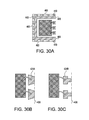
- FIG. 30A is a top-down plan view illustrating a stage in a variation of the method illustrated in accordance with FIGS. 21-30 .
- FIGS. 30B and 30C are fragmentary top-down plan views further illustrating a variation of the method illustrated in accordance with FIGS. 21-30 .
- FIG. 31 is a sectional view depicting a microelectronic package according to an embodiment of the invention.
- FIG. 32 is a sectional view depicting a microelectronic package according to a variation of the embodiment of the invention depicted in FIG. 31 .
- FIG. 33 is a sectional view depicting a microelectronic assembly according to an embodiment of the invention.
- FIG. 34 is a sectional view depicting a microelectronic package according to a variation of the embodiment of the invention depicted in FIG. 32 .
- FIG. 35 is a sectional view depicting a microelectronic package according to a variation of the embodiment of the invention depicted in FIG. 32 .
- FIG. 36 is a top-down plan view corresponding to FIG. 35 .
- FIG. 37A is a sectional view depicting a microelectronic assembly according to an embodiment of the invention.
- FIG. 37B is a top-down plan view depicting a microelectronic assembly according to an embodiment of the invention.
- FIG. 38 is a sectional view depicting a microelectronic assembly according to a variation of the embodiment of the invention depicted in FIG. 37A .
- FIG. 39 is a top-down plan view depicting a microelectronic package in accordance with an embodiment of the invention.
- FIG. 40 is a sectional view corresponding to FIG. 39 .
- FIG. 41 is a sectional view depicting a microelectronic package in accordance with a variation of an embodiment of the invention depicted in FIG. 32 .
- a statement that an electrically conductive element is “at” a surface of the dielectric region or component indicates that, when the surface is not covered or assembled with any other element, the electrically conductive element is available for contact with a theoretical point moving in a direction perpendicular to that surface of the dielectric region from outside the dielectric region or component.
- a terminal or other conductive element which is at a surface of a dielectric region may project from such surface; may be flush with such surface; or may be recessed relative to such surface in a hole or depression in the dielectric region.
- FIG. 1 illustrates a microelectronic assembly 100 in accordance with an embodiment of the invention.
- microelectronic assembly 100 includes a package stack 110 which includes a plurality of stacked microelectronic subassemblies or microelectronic packages 108 , each microelectronic subassembly including one or more microelectronic elements 112 such as a semiconductor chip.
- Microelectronic assembly 100 and other microelectronic assemblies disclosed or referenced herein can provide enhanced storage density which can be especially advantageously provided in systems used in data centers, among which include enterprise systems, government systems, hosted systems, search engine systems, cloud storage, or other large-scale data centers.
- microelectronic element 112 may be a stack of one or more semiconductor chips.
- each of the semiconductor chips may include one or more memory storage arrays, which may include a particular memory type such as nonvolatile memory.
- Nonvolatile memory can be implemented in a variety of technologies some of which include memory cells that incorporate floating gates, such as, for example, flash memory, and others which include memory cells which operate based on magnetic polarities. Flash memory chips are currently in widespread use as solid state storage as an alternative to magnetic fixed disk drives for computing and mobile devices.
- Flash memory chips are also commonly used in portable and readily interchangeable memory drives and cards, such as Universal Serial Bus (USB) memory drives, and memory cards such as Secure Digital or SD cards, microSD cards (trademarks or registered trademarks of SD-3C), compact flash or CF card and the like. Flash memory chips typically have NAND or NOR type devices therein; NAND type devices are common. Other examples of semiconductor chips 112 may also include one or more DRAM, NOR, microprocessor, controller die, etc. or combinations thereof. Each semiconductor chip may be implemented in one of various semiconductor materials such as silicon, germanium, gallium arsenide or one or more other Group III-V semiconductor compounds or Group II-VI semiconductor compounds, etc.
- microelectronic elements 112 in one or more microelectronic subassemblies 108 and in one or more “package stacks” 110 may be a combination of different chip functionalities as described above and a combination of various semiconductor materials as described above.
- a microelectronic element may have a greater number of active devices for providing memory storage array function than for any other function.
- Each microelectronic element e.g., semiconductor chip 112 has a front surface 114 defining a respective plane 116 - x of a plurality of planes 116 - 1 , 116 - 2 , etc.
- Each semiconductor chip 112 has a plurality of contacts 118 at its front surface and an edge surface 120 which extends away from the front surface of such chip.
- Each chip also has a rear surface 122 opposite from its front surface 114 .
- each of the chips in the package stack are shown all oriented in the same direction in FIG. 1
- the front surfaces of one or more of the chips in the package stack can be oriented in the opposite direction such that the front surfaces of at least two of the chips which are adjacent one another would either face each other or would face in opposite directions away from one another.
- each package stack 110 may include a dielectric region 115 that extends between the rear surface 122 - 1 of a first chip 112 - 1 and a rear surface or front surface 114 - 2 of a second chip 112 - 2 that is adjacent to the first chip in the package stack.
- the dielectric region may include one or more adhesive layers or other dielectric material.
- the dielectric region includes at least adhesive layers coupled to each of the opposed front or rear surfaces of adjacent chips in the package stack.
- the dielectric region 115 includes one or more layers of epoxy, elastomer, polyimide or other polymeric material.
- the package stack also includes a plurality of package contacts which may be defined by metal leadframe interconnects 124 electrically coupled to a chip contact 118 on a microelectronic element through a lead.
- each package contact can be electrically coupled with the chip contact 118 at a front surface of a microelectronic element through a trace 126 , the trace extending in a direction generally parallel to the front surface 114 towards an edge surface 120 of the respective chip.
- the traces can be formed by depositing an electrically conductive material.
- the traces can be formed by plating a metal onto and in-between the contacts 118 and the leadframe 306 (See FIG.
- the leadframe can serve as an electrical commoning element in a process that includes electrolytic plating.
- a seed layer therefor can be formed by electroless plating or sputtering.
- the traces 126 can be formed by depositing drops, droplets or lines of electrically conductive polymer material or electrically conductive ink, or alternatively by blanket depositing such material and then removing the material between laterally adjacent contacts on the same microelectronic subassembly or package 108 , and between adjacent portions of the leadframe on the same microelectronic package 108 .
- each of the leadframe interconnects 124 may extend to a peripheral edge 128 or “remote surface” of the respective package 108 .
- a dielectric region or encapsulant region contacts the chip contacts at the front surface of the package, such that the remote surface 128 is spaced apart from the edge surface of the microelectronic element adjacent to the remote surface.
- the encapsulant region can extend from two or more edge surfaces of the microelectronic element to corresponding remote surfaces of the package spaced apart from the edge surfaces.
- the substrate 130 may be a dielectric element or other substrate and which may have one or multiple layers of dielectric material and one or multiple electrically conductive layers thereon.
- the substrate 130 can be formed of various materials, which may or may not include a polymeric component, and may or may not include an inorganic component. Alternatively, the substrate may be wholly or essentially polymeric or may be wholly or essentially inorganic.
- the support element can be formed of a composite material such as glass-reinforced epoxy, e.g., FR-4, a semiconductor material, e.g., Si or GaAs, or glass or ceramic material.
- the substrate can be one that has contacts on a lower surface facing away from the microelectronic assemblies, the contacts configured for surface mounting to another component which can be a card, tray, motherboard, etc., such as via a land grid array (LGA), ball grid array (BGA), or other technique.
- the substrate can be a card component having slide contacts on top and bottom surfaces thereof, such as for insertion into a socket.
- another component such as universal serial bus (USB) controller or other communications controller can be mounted to the substrate and electrically coupled with the microelectronic assembly, such component assisting in or controlling a flow of information between the microelectronic assembly and a system.
- USB universal serial bus
- electrically conductive material 135 such as conductive masses, conductive pillars, stud bumps or other suitable electrically conductive material may be used to electrically connect each of the leadframe interconnects 124 at an end thereof to a corresponding substrate contact 132 .
- the conductive material 135 can be in form of electrically conductive bumps such as masses of solder, tin, indium or eutectic material, or drops or droplets of electrically conductive polymer material or electrically conductive ink on surfaces of the substrate contacts and contacting the leadframe interconnects 124 .
- the electrically conductive material may be applied thereto through a transfer mold of solder bumps, balls or features, or application of solder balls, for example, or may alternatively be deposited on the substrate contacts by plating or depositing a metal or other conductive material.
- the electrically conductive material 135 can be applied by depositing an electrically conductive ink or paste or an electrically conductive polymer material onto an exposed surface of the substrate contact 132 .
- Support element 130 may be organic substrate or semiconducting materials like Si, GaAs, etc. As seen in FIG. 1 , the parallel planes 116 - x defined by the front surfaces of the chips 114 are oriented transverse to, i.e., in a direction non-parallel to, a plane 136 defined by the major surface 134 of the support element.
- a dielectric region 140 which in some cases may be made of or include an encapsulant material, overlies the edge surface 120 of a respective chip. Each chip may have such dielectric region overlying the edge surface thereof.
- the dielectric region 140 may be or may include a molded dielectric region.
- the dielectric region may comprise a polymeric dielectric material, or alternatively a polymeric dielectric material with a filler therein which may have a lower coefficient of thermal expansion than the polymeric material.
- the filler may include particles, flakes or a mesh or scaffold of an inorganic material such as a glass, quartz, ceramic or semiconductor material, among others.
- the parallel planes 116 - x may be oriented in a direction orthogonal to the plane 136 of the support element major surface.
- FIG. 1 shows an example in which the major surface 134 of the support element faces the edge surfaces 120 of each chip.
- An adhesive 142 which may be an underfill, may be applied surrounding the electrical connections between the leadframe interconnects and the substrate contacts and the adhesive may have a function to mechanically reinforce or stiffen such electrical connections and may help the electrical connections withstand stresses due to differential thermal expansion between the chips 112 and the support element 130 .
- a plurality of the microelectronic stacks 110 can be mounted and electrically connected to the substrate contacts 132 .
- the distance in an orthogonal direction between respective package stacks 110 defines a gap 160 which, in some cases may be 100 microns, or may range from 100 to 200 microns in dimension, or may have a greater value.
- an adhesive can be provided, and/or other elements, which may in some cases include a heat spreader as further describe below, or passive components, hardware, or other components which may or may not be electrically interconnected with one or more of the package stacks 110 .
- the leadframe interconnects 124 may extend to and be flush with a peripheral edge surface 128 of the dielectric region 140 of the microelectronic package.
- the leadframe interconnects may be recessed relative to the peripheral edge surface 128 , or may extend beyond the peripheral edge surface 128 .
- the package contacts such as leadframe interconnects 124 project beyond the peripheral edge surface 128
- a leadframe 306 is attached to an adhesive tape 304 such as may be used for dicing or other temporary placement of components during manufacturing and assembly.
- the tape and leadframe may extend beyond that shown in FIGS. 3-4 to encompass a larger area, such as that of a panel, e.g., which typically has dimensions of 500 millimeters by 500 millimeters.
- a plurality of microelectronic elements 312 are attached or otherwise placed face-down towards the tape 304 at locations between portions of the leadframe 306 .
- the front surfaces 114 of the microelectronic elements face toward the tape 304 and the rear surfaces 122 face away therefrom.
- a dielectric material 140 is applied into spaces between the microelectronic elements 312 and the leadframe to form a reconstituted panel 308 .
- the dielectric material covers the rear surfaces 122 and the lead frame as seen in FIG. 6 , but this need not be so in other embodiments.
- the dielectric material typically is an encapsulant as described above, and in some examples can be applied by a molding process to form a molded dielectric encapsulation.
- the tape 304 is removed, leaving the reconstituted panel 308 shown therein with the front faces 114 and contacts 118 of the microelectronic elements 112 exposed. Thereafter, as seen in FIG. 8 , the above-described electrically conductive traces 126 are formed which electrically connect the contacts 118 with portions of the leadframe 306 adjacent thereto.
- a plurality of the reconstituted panels 308 are stacked one atop the other with an adhesive or other dielectric layer 115 between adjacent panels to form a stacked panel assembly 328 .
- the dielectric layer 115 can be omitted when other structure such as a fixture or frame mechanism maintains the positions of the reconstituted panels relative to one another.
- the stacked panel assembly is singulated into individual “package stacks” 110 , each package stack 110 being as described above relative to FIG. 1 .
- the package stacks 110 then are assembled with respective support elements 130 to form the assemblies 100 , 200 seen in FIG. 1 or FIG. 2 .
- the reconstituted panel 308 with electrical conductive traces 126 on them can be singulated first to form individual microelectronic packages. These individual packages are then stacked one atop the other with an adhesive or other dielectric layer 115 between adjacent packages to form a microelectronic stack 110 . The microelectronic stacks 110 then are assembled with respective support elements 130 to form the assemblies 100 , 200 seen in FIG. 1 or FIG. 2 .
- a metal sheet 316 instead of attaching a leadframe to an adhesive tape, a metal sheet 316 , e.g., a foil of copper or a foil having a layered metal structure which includes a foil of copper can be attached to an adhesive tape.
- Leadframes typically have a thickness of 100 micrometers (hereinafter “microns”) in a direction orthogonal to the faces of the microelectronic element.
- the metal sheet 316 in some cases, can be made thinner than the leadframe, for example, ranging from 1 to 99 microns in thickness. Alternatively, the metal sheet 316 can be made thicker than a typical leadframe.
- the metal sheet in some cases can be pre-patterned prior to being attached to the tape 304 .
- FIG. 13 illustrates the metal sheet after patterning performed subsequent to attaching the metal sheet to the tape 304 . Thereafter, the same processing as described above is performed to fabricate a microelectronic assembly 100 or 200 as seen in FIG. 1 or FIG. 2 .
- the words “leadframe interconnect” as used herein refer to portions of such metal sheet 316 which remain in the final microelectronic assembly 100 fabricated in this manner.
- FIG. 14 illustrates a microelectronic subassembly 408 formed in a variation of the above-described process.
- the contacts 118 on adjacent microelectronic elements 112 are disposed near edges of the microelectronic elements such that contacts 118 on an adjacent pair of microelectronic elements are proximate to one another.
- the traces 126 extend from the contacts on each of the adjacent microelectronic elements to the leadframe or metal sheet disposed between the adjacent microelectronic elements.
- the leadframe 306 or metal sheet can be patterned prior to forming the encapsulation such that portions 318 of the leadframe 306 or metal sheet disposed between fingers 346 of the leadframe 306 have smaller thickness than the fingers 346 .
- “fingers” refer to laterally extending portions of the leadframe 306 or of a metal sheet 316 prior to singulation into the package stacks 110 seen in FIG. 10 . Providing the smaller thickness may improve subsequent processing such as the cutting process described above relative to FIG. 10 where the cutting instrument can cut through the portions 318 having the smaller thicknesses.
- FIG. 16 illustrates a further variation in which individual microelectronic subassemblies 108 are directly electrically coupled with one another through the leadframe fingers 346 or metal sheet portions, the traces 126 , or both.
- FIGS. 17-18 illustrate a further variation in which the leadframe fingers extend laterally from a support element 348 of the leadframe which has substantial width in a direction extending between the adjacent edges 120 , 121 of the microelectronic elements shown in FIGS. 17-18 .
- FIGS. 19-20 after the singulation described above referring to FIG. 10 , a portion of the support element 348 , severed from the leadframe fingers 346 , now remains as part of the microelectronic package stack 110 - 2 .
- the severed support element 348 may function as an electrical commoning layer for providing a ground or power connection.
- the severed support element 348 may serve as an embedded heat spreader integrated as a part of microelectronic subassembly 108 .
- an effective heat spreader can be provided for transporting and thermal energy from areas near a support element 130 as seen in FIG. 1 to a top of the assembly remote from the support element.
- fingers 446 of the leadframe 406 extend from a leadframe support element 448 which encompasses an area of the microelectronic element.
- FIG. 22 depicts the leadframe 406 or metal sheet disposed on a tape 304 as described above. Referring to FIGS. 23-24 , a microelectronic element 412 is placed face-up on the tape 304 and wire bonds 444 are formed which electrically connect contacts 418 of the microelectronic element with the fingers 446 .
- FIG. 24 illustrates two examples of wire bonds.
- the ball-bond for the wire bond 444 is formed on the contact 418 of the microelectronic element and a stitch bond is formed on the finger 446 .
- the ball-bond of the wire bond 445 is formed on the finger 446 and the stitch bond is formed on the contact of the microelectronic element.
- An assembly having a lower height can be obtained by using a reverse-bonding technique in which the ball-bond is formed on the element which has a substantially lower height than the other element to which it is connected through the wire bond.
- reverse-bonding technique can help decrease the loop height of the wire bond, effectively reducing a height of the wire-bonded assembly seen in FIGS. 23-24 .
- FIGS. 25-26 illustrate the subassembly after forming a dielectric region 440 thereon, which typically is a dielectric encapsulant such as described above, and which is typically formed by a molding process.
- FIGS. 27-28 illustrate subsequent singulation of the subassembly into individual microelectronic packages 408 , each package 408 including a microelectronic element 412 having contacts 418 electrically connected to individual leadframe interconnects 424 formed by separating the leadframe fingers 446 from other portions of the leadframe.
- FIG. 29 illustrates a stage in which the individual microelectronic packages 408 have been stacked and assembled together one atop the other to form the microelectronic stack 410 .
- a dielectric material or adhesive 415 can mechanically bind adjacent microelectronic packages 408 to one another.
- any of the techniques described above relative to FIG. 1 or FIG. 16 can be used to maintain the positions of the microelectronic packages relative to one another.
- FIG. 30 illustrates an assembly which includes one or more microelectronic package stacks 410 for which the leadframe interconnects 424 of each package stack 410 are electrically coupled with corresponding contacts 132 at a major surface 134 of a support element 130 , e.g., through electrically conductive material 135 as described above.
- each package stack 410 is shown including only two microelectronic packages 408 , although each package stack 410 can include a greater number of microelectronic packages 408 .
- each microelectronic package 408 can be assembled individually with the support element.
- a dielectric stiffening material 142 e.g., an underfill, contacting the remote surfaces of each package at which the package contacts are disposed, and the major surface of the substrate, the stiffening material surrounding each of the connections between the package contacts and the substrate contacts.
- features 133 such as dummy bumps, which can have either electrically conductive or insulating properties, can be disposed at at least a portion of the major surface of the substrate aligned with a gap between package stacks, such features defining flow paths configured to convey the dielectric stiffening material across the gap.
- leadframe elements including leadframe support elements 448 define a discontinuous metal surface at at least one of the remote surfaces 460 of the encapsulation region.
- the extent of cutting required of the leadframe support elements 448 is reduced.
- the cutting instrument can be positioned so as to cut through leadframe fingers 449 at peripheral edges of each microelectronic package rather than through leadframe support elements 448 which extend continuously in the same direction as the path of the cutting instrument. With the reduced cutting provided in this way, a blade or other element of the cutting instrument may be subject to less wear, and other benefits such as improved process window, or less production of debris may be achieved.
- FIGS. 30B and 30C illustrate a further variation in which leadframe interconnects 424 A and 424 B, respectively, may include features, e.g., an advantageous geometry, which assist in locking the leadframe interconnects 424 A or 424 B in place within the dielectric region, e.g., molded dielectric encapsulation of each respective package.
- the cutting instrument severs the leadframe fingers at lines 436 in each example to form the leadframe interconnects 424 A or 424 B
- the features characterized by a widening of a lateral dimension of the leadframe fingers in a direction away from lines 436 —assists in avoiding the leadframe interconnects 424 A, 424 B from being released from their attachments with the molded dielectric encapsulation after such singulation process.
- FIG. 31 further depicts the microelectronic package 408 and thicknesses of elements therein in a direction orthogonal to a plane 405 in which a major surface 404 of the package 408 lies.
- the microelectronic element may have a thickness 452 ranging from 10 to 100 microns.
- the leadframe interconnect 424 may have a thickness 454 typically of 100 microns when the leadframe interconnect is formed by severing leadframe fingers from a standard leadframe. Although thickness 454 of the leadframe interconnect is shown to be 100 microns, the thickness 454 can be smaller or larger than 100 microns.
- each microelectronic package 408 may have a thickness 456 of 150-200 microns to account for loop height of the wire bonds 444 extending above top surfaces of the leadframe interconnects.
- FIG. 32 an alternative microelectronic package 508 is illustrated in FIG. 32 which includes first and second microelectronic elements 512 - 1 and 512 - 2 , each having contacts 518 interconnected via wire bonds 544 with the leadframe interconnects 524 .
- the microelectronic elements 512 - 1 and 512 - 2 are stacked in a staggered manner such that the contacts 518 on the lower positioned microelectronic element 512 - 1 are disposed beyond an adjacent edge surface 520 of the higher positioned microelectronic element 512 - 2 .
- corresponding contacts 518 on each microelectronic element 512 - 1 and 512 - 2 can each be wire bonded directly to the same leadframe interconnect 524 via wire bonds 544 .
- corresponding contacts 518 on the microelectronic element 512 - 1 and 512 - 2 can be wire bonded with one another via wire bond 545 , and only one of the microelectronic elements 512 - 1 or 512 - 2 can be wire bonded directly to the leadframe interconnect 524 . It is not necessary, although it is possible, for the contacts 518 of each microelectronic element to be both directly wire bonded to the corresponding leadframe interconnect 524 , and to be wire-bonded with one another.
- FIG. 33 further illustrates a microelectronic assembly 500 which includes one or more “package stacks” 510 each package stack formed by assembling a plurality of multi-chip microelectronic packages 508 each as described relative to FIG. 32 .
- the multi-chip packages in each package stack 510 are electrically interconnected with contacts 132 at a surface of a support element 130 in a manner such as described above relative to FIG. 30 .
- An advantage of providing more than one microelectronic element electrically coupled with the leadframe interconnects in an individual microelectronic package is a potential to increase a density of interconnection of the microelectronic elements in a microelectronic assembly 500 relative to the contacts 132 of the support element 130 .
- microelectronic packages 508 incorporating two chips per package are electrically interconnected with the substrate contacts 132 at an effective pitch which is one half the pitch of interconnection between adjacent microelectronic packages 508 in each package stack 510 .
- a thickness 554 of each leadframe interconnect in a vertical direction of the microelectronic package may be 100 microns for a standard leadframe thickness and a thickness 556 of the microelectronic package can be 200 microns, for example.
- the pitch among substrate contacts 132 is 200 microns, because there are two microelectronic elements in each package which are electrically coupled with the leadframe interconnects of such package, the effective pitch of interconnection among adjacent microelectronic elements in each of the package stacks 510 seen in FIG. 33 can be 100 microns.
- microelectronic elements When the microelectronic elements are microelectronic elements having memory storage arrays therein, corresponding chip contacts on all of the microelectronic elements in the package can be electrically coupled with a single package contact of the package. The same can apply to most or all of the chip contacts of each microelectronic element, except for chip contacts assigned to receive signals routed uniquely to one of the microelectronic elements, such as a chip select input, for example. The same applies to microelectronic elements which provide non-volatile memory storage array function, such non-volatile memory storage array implemented by a greater number of active devices in the microelectronic element than for any other function of the microelectronic element.
- the number of microelectronic elements stacked one above the other in each microelectronic package can range from a small number such as one or two to a much larger number, for example, eight, ten or even greater.
- four microelectronic elements can be stacked within a single package and are electrically coupled with the package contacts, e.g., leadframe interconnects of such package.
- eight microelectronic elements can be stacked within a single package and are electrically coupled with the leadframe interconnects, in a variation of the package as seen in FIG. 32 .
- a microelectronic package 528 can include leadframe interconnects 534 which are each at a lower surface 532 and at an upper surface 530 of the microelectronic package and, thus, are available for connection with external components at these lower and upper surfaces 532 , 530 .
- each leadframe interconnect may include a ledge 535 to which wire bonds are joined and electrically coupled to the contacts of the microelectronic elements 512 - 1 and 512 - 2 , and may further include a portion 536 projecting above a height of the ledge 535 and at the upper surface 530 of the microelectronic package.
- each microelectronic package may include three, four, or an even greater number of microelectronic elements arranged in an offset stack as seen in FIG. 32 or 34 and electrically interconnected with the leadframe interconnects which are provided in such microelectronic package.
- a microelectronic package 508 modified in accordance with another arrangement to include four microelectronic elements instead of two would yield an effective pitch of 50 microns for interconnection with each microelectronic element therein.
- FIGS. 35 and 36 illustrate a microelectronic package 608 according to a variation of the embodiment described above relative to FIG. 32 in which a chip 612 - 1 in microelectronic subassembly or package 608 has a major surface 622 bonded to a major surface of a metal die attach pad 623 portion of the leadframe.
- the major surface of the die attach pad can be recessed below a height of the top surfaces 626 of the leadframe interconnects, and thus may accommodate a height of the topmost front surface of one or more microelectronic elements 612 - 1 , 612 - 2 .
- the recessed major surface of the die attach pad accommodates a thickness of a first microelectronic element 612 - 1 which may be bonded directly to the die attach pad 623 .
- the recessed major surface of the die attach pad accommodates thicknesses of the first and the second microelectronic elements 612 - 1 and 612 - 2 .
- the leadframe may further include a metal member 628 similar to the metal member 348 described above relative to FIG.
- the metal member 628 is elongated in a direction 634 which is parallel to an adjacent edge surface 636 of the at least one microelectronic element 612 - 1 and 612 - 2 of the package 608 .
- a surface of the metal member within the plane 640 can define an edge surface of the microelectronic package 608 .
- the microelectronic package may likewise include additional second and third metal members 644 and 646 which have length elongated in directions parallel to the respective adjacent edges of the microelectronic element.
- the metal members 644 , 646 may have surfaces which define edge surfaces of the microelectronic package, and, like metal member 628 , may extend to a greater height than the die attach pad 623 which accommodates the one or more microelectronic elements 612 - 1 and 612 - 2 between the height of an upwardly-facing surface of the die attach pad 623 and the height of a top surface 630 of the metal member.
- the metal members 644 and 646 are portions of the die attach pad 623 which extend to opposite edges of the die attach pad 623 .
- the height of a top surface 630 of the metal member 628 , 644 and/or 646 may be higher or lower than the front or active surface 632 of the microelectronic element 612 - 2 .
- the die attach pad and metal members coupled thereto may provide even greater thermal and electrical conductivity, such as for purposes of transferring heat or providing power or ground connectivity.
- a structure which includes the die attach pad and one or more of the above-described metal members 628 , 644 and/or 646 may help avoid coupling of unwanted electromagnetic interference between the one or more microelectronic elements 612 - 1 and 612 - 2 and the environment external to the metal members.
- FIGS. 37A-B illustrate a microelectronic assembly 610 in accordance with a particular example in which a microelectronic package of the type described above relative to FIGS. 35-36 is combined with other microelectronic packages 508 of the type described above relative to FIG. 32 .
- the die attach pad 623 with one or more metal members extending therefrom can function as a heat spreader facilitating conduction of thermal energy away from microelectronic elements therein.
- a plurality of the microelectronic assemblies can be coupled to contacts at a surface 134 of a substrate.
- eight microelectronic assemblies are shown, each which includes four microelectronic packages such as the package 508 or 608 , for example.
- each encapsulated microelectronic package of each assembly may include one to eight stacked microelectronic elements.
- the assembly of the substrate coupled the plurality of eight microelectronic assemblies shown will include from 32 to 256 microelectronic elements. Referring to FIG.
- a plurality of microelectronic packages 609 are arranged together in a stacked configuration, wherein each microelectronic package 609 is the same as a microelectronic package 608 except in this case, each substantially rigid metal member or leadframe element 629 and each leadframe interconnect 625 extends a full thickness of the microelectronic package 609 in a vertical direction of the microelectronic package.
- the metal members 629 of the microelectronic packages are joined together through with a thermally and/or electrically conductive adhesive material 616 bonding the die attach pad 623 of each package to the metal members and a surface of the dielectric region 640 of another microelectronic package immediately adjacent and below the die attach pad of the respective microelectronic package.
- the microelectronic element has an edge surface 820 along which contacts 818 of the microelectronic element are disposed, and the leadframe includes a metal member 828 parallel to and elongated in a direction of a length of the interconnect edge surface.
- the metal member 828 may surround the one or more microelectronic elements 812 within the package and have a ring-like geometry.
- the metal member may function as an element for electrical connection of the contacts 818 with ground or to other steady voltage such as a reference voltage or a power supply voltage.
- some contacts 818 may be electrically interconnected directly with the metal member, while others of the contacts are electrically interconnected directly with leadframe interconnects 826 which are disposed beyond the metal member and which may be at a periphery of the microelectronic package 808 .
- some of the leadframe interconnects 826 can be electrically interconnected directly with the metal member 828 and may not have a direct electrical interconnection with a contact 818 of the microelectronic element 812 .
- the electrical interconnections between the contacts, the metal member, and the leadframe interconnects can be through wire bonds. However, other interconnection arrangements are possible, such as further described herein.
- the contacts 938 of a microelectronic element 912 are electrically interconnected with the leadframe interconnects 926 of the microelectronic package 908 through electrically conductive structure extending above the front surfaces of the microelectronic elements.
- the electrical interconnections may include vias 938 extending from the contacts and traces 942 extending in a lateral direction relative to the contacts.
- the electrical interconnections may include free standing wire bond connections extending from the contacts to the traces 942 , similar to that referred to as bond via array (“BVA”) technology such as disclosed, for example, in FIG. 7 of commonly owned U.S. application Ser. No. 13/462,158, now U.S. Pat. No. 8,619,659, incorporated by reference herein.
- electrically conductive vias 938 can extend through a dielectric region 940 in a vertical direction above the front surfaces of the microelectronic elements and traces 940 can extend above a surface of the dielectric region 940 .
- the traces 942 may contact or be supported on a dielectric layer 946 added above the dielectric region 940 , which may be of a different material than the dielectric region 940 .
- the structures and processing above relating to use of a patterned or unpatterned metal sheet can be utilized instead of a leadframe and references to portions of a leadframe such as leadframe fingers, leadframe interconnects, support members and metal members apply equally to portions of such metal sheet.
Abstract
Description
Claims (28)
Priority Applications (2)
| Application Number | Priority Date | Filing Date | Title |
|---|---|---|---|
| US14/883,864 US9490195B1 (en) | 2015-07-17 | 2015-10-15 | Wafer-level flipped die stacks with leadframes or metal foil interconnects |
| US15/342,744 US9666513B2 (en) | 2015-07-17 | 2016-11-03 | Wafer-level flipped die stacks with leadframes or metal foil interconnects |
Applications Claiming Priority (4)
| Application Number | Priority Date | Filing Date | Title |
|---|---|---|---|
| US201562194051P | 2015-07-17 | 2015-07-17 | |
| US201562219015P | 2015-09-15 | 2015-09-15 | |
| US201562222737P | 2015-09-23 | 2015-09-23 | |
| US14/883,864 US9490195B1 (en) | 2015-07-17 | 2015-10-15 | Wafer-level flipped die stacks with leadframes or metal foil interconnects |
Related Child Applications (1)
| Application Number | Title | Priority Date | Filing Date |
|---|---|---|---|
| US15/342,744 Continuation US9666513B2 (en) | 2015-07-17 | 2016-11-03 | Wafer-level flipped die stacks with leadframes or metal foil interconnects |
Publications (1)
| Publication Number | Publication Date |
|---|---|
| US9490195B1 true US9490195B1 (en) | 2016-11-08 |
Family
ID=57211205
Family Applications (2)
| Application Number | Title | Priority Date | Filing Date |
|---|---|---|---|
| US14/883,864 Active US9490195B1 (en) | 2015-07-17 | 2015-10-15 | Wafer-level flipped die stacks with leadframes or metal foil interconnects |
| US15/342,744 Active US9666513B2 (en) | 2015-07-17 | 2016-11-03 | Wafer-level flipped die stacks with leadframes or metal foil interconnects |
Family Applications After (1)
| Application Number | Title | Priority Date | Filing Date |
|---|---|---|---|
| US15/342,744 Active US9666513B2 (en) | 2015-07-17 | 2016-11-03 | Wafer-level flipped die stacks with leadframes or metal foil interconnects |
Country Status (1)
| Country | Link |
|---|---|
| US (2) | US9490195B1 (en) |
Cited By (13)
| Publication number | Priority date | Publication date | Assignee | Title |
|---|---|---|---|---|
| US20170018529A1 (en) * | 2015-07-17 | 2017-01-19 | Invensas Corporation | Flipped die stack |
| US9728524B1 (en) | 2016-06-30 | 2017-08-08 | Invensas Corporation | Enhanced density assembly having microelectronic packages mounted at substantial angle to board |
| US20170294410A1 (en) * | 2016-04-11 | 2017-10-12 | Invensas Corporation | Microelectronic packages having stacked die and wire bond interconnects |
| US20170317054A1 (en) * | 2016-05-02 | 2017-11-02 | Taiwan Semiconductor Manufacturing Co., Ltd. | Package structure and method for manufacturing the same |
| US9859257B2 (en) | 2015-12-16 | 2018-01-02 | Invensas Corporation | Flipped die stacks with multiple rows of leadframe interconnects |
| US9871019B2 (en) | 2015-07-17 | 2018-01-16 | Invensas Corporation | Flipped die stack assemblies with leadframe interconnects |
| US10354978B1 (en) * | 2018-01-10 | 2019-07-16 | Powertech Technology Inc. | Stacked package including exterior conductive element and a manufacturing method of the same |
| CN111063664A (en) * | 2019-12-27 | 2020-04-24 | 华天科技(西安)有限公司 | Modularized multi-chip packaging structure and packaging method thereof |
| CN111863738A (en) * | 2020-07-28 | 2020-10-30 | 南通通富微电子有限公司 | Semiconductor packaging device |
| CN111883439A (en) * | 2020-07-28 | 2020-11-03 | 南通通富微电子有限公司 | Chip packaging method |
| US11482500B2 (en) * | 2018-02-27 | 2022-10-25 | Amkor Technology Singapore Holding Pte. Ltd. | Method of forming an electronic device structure having an electronic component with an on-edge orientation and related structures |
| US11495521B2 (en) * | 2019-08-30 | 2022-11-08 | Delta Electronics (Shanghai) Co., Ltd | Power module and method for manufacturing the same |
| WO2024031767A1 (en) * | 2022-08-10 | 2024-02-15 | 长鑫存储技术有限公司 | Semiconductor structure and method for manufacturing same |
Families Citing this family (6)
| Publication number | Priority date | Publication date | Assignee | Title |
|---|---|---|---|---|
| CN111106078A (en) * | 2019-12-16 | 2020-05-05 | 山东砚鼎电子科技有限公司 | Multi-chip integrated packaging structure |
| CN110943041A (en) * | 2019-12-16 | 2020-03-31 | 山东砚鼎电子科技有限公司 | Semiconductor structure with side surface led out, manufacturing method thereof and stacking structure |
| CN111863719B (en) * | 2020-07-28 | 2022-07-19 | 南通通富微电子有限公司 | Chip interconnection method |
| CN111863641B (en) * | 2020-07-28 | 2022-06-21 | 南通通富微电子有限公司 | Chip packaging method |
| CN111863717B (en) * | 2020-07-28 | 2022-07-15 | 南通通富微电子有限公司 | Chip interconnection method |
| WO2022037754A1 (en) * | 2020-08-17 | 2022-02-24 | Huawei Technologies Co., Ltd. | A method for manufacturing a die assembly |
Citations (268)
| Publication number | Priority date | Publication date | Assignee | Title |
|---|---|---|---|---|
| US3639888A (en) | 1970-01-15 | 1972-02-01 | Ind Electronic Hardware Corp | Printed circuit board connector |
| US4323914A (en) | 1979-02-01 | 1982-04-06 | International Business Machines Corporation | Heat transfer structure for integrated circuit package |
| US4336551A (en) | 1977-05-30 | 1982-06-22 | Hitachi, Ltd. | Thick-film printed circuit board and method for producing the same |
| US4363076A (en) | 1980-12-29 | 1982-12-07 | Honeywell Information Systems Inc. | Integrated circuit package |
| US4500905A (en) | 1981-09-30 | 1985-02-19 | Tokyo Shibaura Denki Kabushiki Kaisha | Stacked semiconductor device with sloping sides |
| US4706166A (en) | 1986-04-25 | 1987-11-10 | Irvine Sensors Corporation | High-density electronic modules--process and product |
| US4726777A (en) | 1986-06-10 | 1988-02-23 | Amp Incorporated | Socket for zig-zag inline package |
| US4784972A (en) | 1984-08-18 | 1988-11-15 | Matsushita Electric Industrial Co. Ltd. | Method of joining beam leads with projections to device electrodes |
| US4951122A (en) | 1987-05-27 | 1990-08-21 | Hitachi, Ltd. | Resin-encapsulated semiconductor device |
| US4967262A (en) | 1989-11-06 | 1990-10-30 | Micron Technology, Inc. | Gull-wing zig-zag inline lead package having end-of-package anchoring pins |
| US5047837A (en) | 1988-08-15 | 1991-09-10 | Hitachi, Ltd. | Semiconductor device with heat transfer cap |
| US5107325A (en) | 1989-04-17 | 1992-04-21 | Seiko Epson Corporation | Structure and method of packaging a semiconductor device |
| US5138438A (en) | 1987-06-24 | 1992-08-11 | Akita Electronics Co. Ltd. | Lead connections means for stacked tab packaged IC chips |
| US5200362A (en) | 1989-09-06 | 1993-04-06 | Motorola, Inc. | Method of attaching conductive traces to an encapsulated semiconductor die using a removable transfer film |
| US5218234A (en) | 1991-12-23 | 1993-06-08 | Motorola, Inc. | Semiconductor device with controlled spread polymeric underfill |
| US5304737A (en) | 1991-10-15 | 1994-04-19 | Goldstar Electron Co., Ltd. | Semiconductor package |
| US5311401A (en) | 1991-07-09 | 1994-05-10 | Hughes Aircraft Company | Stacked chip assembly and manufacturing method therefor |
| US5331591A (en) | 1993-02-01 | 1994-07-19 | At&T Bell Laboratories | Electronic module including a programmable memory |
| US5334872A (en) | 1990-01-29 | 1994-08-02 | Mitsubishi Denki Kabushiki Kaisha | Encapsulated semiconductor device having a hanging heat spreading plate electrically insulated from the die pad |
| US5347428A (en) | 1992-12-03 | 1994-09-13 | Irvine Sensors Corporation | Module comprising IC memory stack dedicated to and structurally combined with an IC microprocessor chip |
| FR2704690A1 (en) | 1993-04-27 | 1994-11-04 | Thomson Csf | Method for encapsulating semiconductor wafers, device obtained by this process and application to the interconnection of wafers in three dimensions. |
| US5365106A (en) | 1992-10-27 | 1994-11-15 | Kabushiki Kaisha Toshiba | Resin mold semiconductor device |
| US5434745A (en) | 1994-07-26 | 1995-07-18 | White Microelectronics Div. Of Bowmar Instrument Corp. | Stacked silicon die carrier assembly |
| US5466634A (en) | 1994-12-20 | 1995-11-14 | International Business Machines Corporation | Electronic modules with interconnected surface metallization layers and fabrication methods therefore |
| US5534729A (en) | 1993-06-29 | 1996-07-09 | Texas Instruments Incorporated | Integrated circuit lead frame for coupling to non-neighboring bond pads |
| US5538758A (en) | 1995-10-27 | 1996-07-23 | Specialty Coating Systems, Inc. | Method and apparatus for the deposition of parylene AF4 onto semiconductor wafers |
| US5571754A (en) | 1995-07-26 | 1996-11-05 | International Business Machines Corporation | Method of fabrication of endcap chip with conductive, monolithic L-connect for multichip stack |
| US5592019A (en) | 1994-04-19 | 1997-01-07 | Mitsubishi Denki Kabushiki Kaisha | Semiconductor device and module |
| US5616953A (en) | 1994-09-01 | 1997-04-01 | Micron Technology, Inc. | Lead frame surface finish enhancement |
| US5629566A (en) | 1994-08-15 | 1997-05-13 | Kabushiki Kaisha Toshiba | Flip-chip semiconductor devices having two encapsulants |
| US5675180A (en) | 1994-06-23 | 1997-10-07 | Cubic Memory, Inc. | Vertical interconnect process for silicon segments |
| US5691248A (en) | 1995-07-26 | 1997-11-25 | International Business Machines Corporation | Methods for precise definition of integrated circuit chip edges |
| US5698895A (en) | 1994-06-23 | 1997-12-16 | Cubic Memory, Inc. | Silicon segment programming method and apparatus |
| US5716759A (en) | 1993-09-02 | 1998-02-10 | Shellcase Ltd. | Method and apparatus for producing integrated circuit devices |
| US5721151A (en) | 1995-06-07 | 1998-02-24 | Lsi Logic Corporation | Method of fabricating a gate array integrated circuit including interconnectable macro-arrays |
| US5731631A (en) | 1996-02-01 | 1998-03-24 | Mitsubishi Denki Kabushiki Kaisha | Semiconductor device with tape automated bonding element |
| US5737191A (en) | 1995-04-07 | 1998-04-07 | Shinko Electric Industries Co., Ltd. | Structure and process for mounting semiconductor chip |
| US5870351A (en) | 1994-10-21 | 1999-02-09 | The Board Of Trustees Of The Leland Stanford Junior University | Broadband microfabriated ultrasonic transducer and method of fabrication |
| WO1999007015A1 (en) | 1997-07-29 | 1999-02-11 | Cubic Memory, Inc. | Conductive epoxy flip-chip on chip |
| WO1999009599A2 (en) | 1997-08-21 | 1999-02-25 | Cubic Memory, Inc. | Vertical interconnect process for silicon segments with dielectric isolation |
| US5879965A (en) | 1997-06-19 | 1999-03-09 | Micron Technology, Inc. | Plastic lead frames for semiconductor devices, packages including same, and methods of fabrication |
| US5891761A (en) | 1994-06-23 | 1999-04-06 | Cubic Memory, Inc. | Method for forming vertical interconnect process for silicon segments with thermally conductive epoxy preform |
| US5910687A (en) | 1997-01-24 | 1999-06-08 | Chipscale, Inc. | Wafer fabrication of die-bottom contacts for electronic devices |
| US5946545A (en) | 1994-03-30 | 1999-08-31 | Internatinal Business Machines Corporation | Semiconductor stack structures and fabrication/sparing methods utilizing programmable spare circuit |
| JPH11260851A (en) | 1998-03-11 | 1999-09-24 | Matsushita Electric Ind Co Ltd | Semiconductor device and its manufacture |
| US5965947A (en) | 1996-08-20 | 1999-10-12 | Samsung Electronics Co., Ltd. | Structure of a semiconductor package including chips bonded to die bonding pad with conductive adhesive and chips bonded with non-conductive adhesive containing insulating beads |
| US6030854A (en) | 1996-03-29 | 2000-02-29 | Intel Corporation | Method for producing a multilayer interconnection structure |
| US6034438A (en) | 1996-10-18 | 2000-03-07 | The Regents Of The University Of California | L-connect routing of die surface pads to the die edge for stacking in a 3D array |
| US6071139A (en) | 1998-03-31 | 2000-06-06 | Micron Technology, Inc. | Locking assembly for securing semiconductor device to carrier substrate |
| US6087716A (en) | 1997-02-03 | 2000-07-11 | Nec Corporation | Semiconductor device package having a connection substrate with turned back leads and method thereof |
| US6107164A (en) | 1998-08-18 | 2000-08-22 | Oki Electric Industry Co., Ltd. | Using grooves as alignment marks when dicing an encapsulated semiconductor wafer |
| JP2000269411A (en) | 1999-03-17 | 2000-09-29 | Shinko Electric Ind Co Ltd | Semiconductor device and manufacture thereof |
| EP1041624A1 (en) | 1999-04-02 | 2000-10-04 | Interuniversitair Microelektronica Centrum Vzw | Method of transferring ultra-thin substrates and application of the method to the manufacture of a multilayer thin film device |
| US6175158B1 (en) | 1998-09-08 | 2001-01-16 | Lucent Technologies Inc. | Interposer for recessed flip-chip package |
| US6225689B1 (en) | 1998-08-21 | 2001-05-01 | Micron Technology, Inc. | Low profile multi-IC chip package connector |
| US6228686B1 (en) | 1995-09-18 | 2001-05-08 | Tessera, Inc. | Method of fabricating a microelectronic assembly using sheets with gaps to define lead regions |
| US6255726B1 (en) | 1994-06-23 | 2001-07-03 | Cubic Memory, Inc. | Vertical interconnect process for silicon segments with dielectric isolation |
| KR20010062722A (en) | 1999-12-28 | 2001-07-07 | 루이스 에이. 헥트 | System for testing bare ic chips and a socket for such chips |
| US6262476B1 (en) | 1998-07-27 | 2001-07-17 | Siemens Aktiengesellschaft | Composite member composed of at least two integrated circuits and method for the manufacture of a composite member composed of at least two integrated circuits |
| JP2001210782A (en) | 2000-01-27 | 2001-08-03 | Seiko Epson Corp | Semiconductor chip, multi-chip package, semiconductor device, and electronic equipment using it |
| WO2001064344A2 (en) | 2000-03-02 | 2001-09-07 | Microchips, Inc. | Microfabricated devices for the storage and selective exposure of chemicals and devices |
| US6297657B1 (en) | 1999-01-11 | 2001-10-02 | Wentworth Laboratories, Inc. | Temperature compensated vertical pin probing device |
| US6303977B1 (en) | 1998-12-03 | 2001-10-16 | Texas Instruments Incorporated | Fully hermetic semiconductor chip, including sealed edge sides |
| US20010031548A1 (en) | 1997-10-20 | 2001-10-18 | Peter Elenius | Method for forming chip scale package |
| US6315856B1 (en) | 1998-03-19 | 2001-11-13 | Kabushiki Kaisha Toshiba | Method of mounting electronic component |
| US6326244B1 (en) | 1998-09-03 | 2001-12-04 | Micron Technology, Inc. | Method of making a cavity ball grid array apparatus |
| US6326689B1 (en) | 1999-07-26 | 2001-12-04 | Stmicroelectronics, Inc. | Backside contact for touchchip |
| US6338980B1 (en) | 1999-08-13 | 2002-01-15 | Citizen Watch Co., Ltd. | Method for manufacturing chip-scale package and manufacturing IC chip |
| US20020006686A1 (en) | 2000-07-12 | 2002-01-17 | Cloud Eugene H. | Die to die connection method and assemblies and packages including dice so connected |
| TW475244B (en) | 2000-09-29 | 2002-02-01 | Ind Tech Res Inst | Stacked type module packaging structure and the generation method thereof |
| US6351030B2 (en) | 1997-09-29 | 2002-02-26 | International Business Machines Corporation | Electronic package utilizing protective coating |
| US20020027257A1 (en) | 2000-06-02 | 2002-03-07 | Kinsman Larry D. | Method for fabricating a chip scale package using wafer level processing and devices resulting therefrom |
| US20020045290A1 (en) | 1996-02-20 | 2002-04-18 | Michael B. Ball | Flip chip and conventional stack |
| US20020096349A1 (en) | 2001-01-24 | 2002-07-25 | Harry Hedler | Electronic component with a semiconductor chip and method of producing the electronic component |
| US20020127775A1 (en) | 1999-12-23 | 2002-09-12 | Rambus Inc. | Redistributed bond pads in stacked integrated circuit die package |
| CN2512114Y (en) | 2001-10-31 | 2002-09-18 | 威盛电子股份有限公司 | Duplicated piled reversing welding-ball matrix package body |
| US6472746B2 (en) | 2000-08-02 | 2002-10-29 | Fujitsu Limited | Semiconductor device having bonding wires serving as external connection terminals |
| US6476467B2 (en) | 1997-01-31 | 2002-11-05 | Hitachi, Ltd. | Semiconductor device and process for producing the same |
| US20020168798A1 (en) | 1996-10-31 | 2002-11-14 | Glenn Thomas P. | Method of making near chip size integrated circuit package |
| US20020180010A1 (en) | 1996-11-21 | 2002-12-05 | Kunihiro Tsubosaki | Semiconductor device and manufacturing method thereof |
| US20020187260A1 (en) | 2001-05-30 | 2002-12-12 | Sheppard Norman F. | Conformal coated microchip reservoir devices |
| US20020190368A1 (en) | 2001-06-19 | 2002-12-19 | Kabushiki Kaishi Toshiba | Semiconductor laminated module |
| US20030038357A1 (en) | 2001-08-24 | 2003-02-27 | Derderian James M. | Spacer for semiconductor devices, semiconductor devices and assemblies including the spacer, and methods |
| US20030038353A1 (en) | 2001-08-23 | 2003-02-27 | Derderian James M. | Assemblies including stacked semiconductor devices separated by discrete conductive elements therebetween, packages including the assemblies, and methods |
| US20030038356A1 (en) | 2001-08-24 | 2003-02-27 | Derderian James M | Semiconductor devices including stacking spacers thereon, assemblies including the semiconductor devices, and methods |
| US20030071338A1 (en) | 2001-10-16 | 2003-04-17 | Jeung Boon Suan | Apparatus and method for leadless packaging of semiconductor devices |
| US20030092326A1 (en) | 2000-06-16 | 2003-05-15 | Hidenobu Nishikawa | Electronic parts packaging method and electronic parts package |
| JP2003142518A (en) | 2001-11-02 | 2003-05-16 | Nec Electronics Corp | Device and method for manufacturing semiconductor, semiconductor device, and electronic device |
| US20030096454A1 (en) | 2001-11-16 | 2003-05-22 | Poo Chia Yong | Stackable semiconductor package and wafer level fabrication method |
| US6569709B2 (en) | 2001-10-15 | 2003-05-27 | Micron Technology, Inc. | Assemblies including stacked semiconductor devices separated a distance defined by adhesive material interposed therebetween, packages including the assemblies, and methods |
| US20030099085A1 (en) | 2001-11-26 | 2003-05-29 | Delaware Capital Formation, Inc. | Surface flashover resistant capacitors and method for producing same |
| JP2003163324A (en) | 2001-11-27 | 2003-06-06 | Nec Corp | Unit semiconductor device and manufacturing method thereof, and three-dimensional laminated semiconductor device |
| USD475981S1 (en) | 2002-03-29 | 2003-06-17 | Mitsubishi Denki Kabushiki Kaisha | Integrated circuits substrate |
| US6580165B1 (en) | 2000-11-16 | 2003-06-17 | Fairchild Semiconductor Corporation | Flip chip with solder pre-plated leadframe including locating holes |
| US20030122243A1 (en) | 2001-12-31 | 2003-07-03 | Jin-Yuan Lee | Integrated chip package structure using organic substrate and method of manufacturing the same |
| US6593648B2 (en) | 2000-08-31 | 2003-07-15 | Seiko Epson Corporation | Semiconductor device and method of making the same, circuit board and electronic equipment |
| US20030143819A1 (en) | 2002-01-25 | 2003-07-31 | Infineon Technologies Ag | Method of producing semiconductor chips with a chip edge guard, in particular for wafer level packaging chips |
| US20030148597A1 (en) | 2002-01-09 | 2003-08-07 | Tan Hock Chuan | Stacked die in die BGA package |
| US6607938B2 (en) | 2001-07-19 | 2003-08-19 | Samsung Electronics Co., Ltd. | Wafer level stack chip package and method for manufacturing same |
| US6607941B2 (en) | 2002-01-11 | 2003-08-19 | National Semiconductor Corporation | Process and structure improvements to shellcase style packaging technology |
| US20030162369A1 (en) | 2002-02-26 | 2003-08-28 | Seiko Epson Corporation | Semiconductor device and method for fabricating the same |
| US6621172B2 (en) | 1999-09-03 | 2003-09-16 | Seiko Epson Corporation | Semiconductor device and method of fabricating the same, circuit board, and electronic equipment |
| US6621155B1 (en) | 1999-12-23 | 2003-09-16 | Rambus Inc. | Integrated circuit device having stacked dies and impedance balanced transmission lines |
| US6624505B2 (en) | 1998-02-06 | 2003-09-23 | Shellcase, Ltd. | Packaged integrated circuits and methods of producing thereof |
| US20030209772A1 (en) | 2002-05-13 | 2003-11-13 | National Semiconductor Corporation | Electrical die contact structure and fabrication method |
| US6656827B1 (en) | 2002-10-17 | 2003-12-02 | Taiwan Semiconductor Manufacturing Co., Ltd. | Electrical performance enhanced wafer level chip scale package with ground |
| US6667543B1 (en) | 2002-10-29 | 2003-12-23 | Motorola, Inc. | Optical sensor package |
| US6670701B2 (en) | 2001-02-01 | 2003-12-30 | Mitsubishi Denki Kabushiki Kaisha | Semiconductor module and electronic component |
| US6674159B1 (en) | 2000-05-16 | 2004-01-06 | Sandia National Laboratories | Bi-level microelectronic device package with an integral window |
| JP2004047702A (en) | 2002-07-11 | 2004-02-12 | Toshiba Corp | Semiconductor device laminated module |
| US6706971B2 (en) | 2001-01-26 | 2004-03-16 | Irvine Sensors Corporation | Stackable microcircuit layer formed from a plastic encapsulated microcircuit |
| US6717061B2 (en) | 2001-09-07 | 2004-04-06 | Irvine Sensors Corporation | Stacking of multilayer modules |
| JP2004119473A (en) | 2002-09-24 | 2004-04-15 | Seiko Epson Corp | Semiconductor device, its manufacturing method, circuit board, and electronic apparatus |
| US6722213B2 (en) | 2000-02-06 | 2004-04-20 | Minitubes Gmbh | Temperature-adjusted sampler for fluids |
| US6737743B2 (en) | 2001-07-10 | 2004-05-18 | Kabushiki Kaisha Toshiba | Memory chip and semiconductor device using the memory chip and manufacturing method of those |
| JP2004153130A (en) | 2002-10-31 | 2004-05-27 | Olympus Corp | Semiconductor device and its manufacturing method |
| JP2004158536A (en) | 2002-11-05 | 2004-06-03 | Fujitsu Ltd | Semiconductor device and method for manufacturing the same |
| US6750547B2 (en) | 2001-12-26 | 2004-06-15 | Micron Technology, Inc. | Multi-substrate microelectronic packages and methods for manufacture |
| US20040113283A1 (en) | 2002-03-06 | 2004-06-17 | Farnworth Warren M. | Method for fabricating encapsulated semiconductor components by etching |
| US6756252B2 (en) | 2002-07-17 | 2004-06-29 | Texas Instrument Incorporated | Multilayer laser trim interconnect method |
| JP2004214548A (en) | 2003-01-08 | 2004-07-29 | Mitsubishi Electric Corp | Component-built-in board type module, manufacturing method thereof, board having same, and manufacturing method thereof |
| US20040150095A1 (en) | 2003-01-30 | 2004-08-05 | Endicott Interconnect Technologies, Inc. | Stacked chip electronic package having laminate carrier and method of making same |
| US6777767B2 (en) | 1999-12-10 | 2004-08-17 | Shellcase Ltd. | Methods for producing packaged integrated circuit devices & packaged integrated circuit devices produced thereby |
| CN1531069A (en) | 2003-03-13 | 2004-09-22 | ������������ʽ���� | Electronic device and producing method thereof |
| US20040198033A1 (en) | 2002-08-20 | 2004-10-07 | Lee Teck Kheng | Double bumping of flexible substrate for first and second level interconnects |
| US20040195667A1 (en) | 2003-04-04 | 2004-10-07 | Chippac, Inc | Semiconductor multipackage module including processor and memory package assemblies |
| US6802446B2 (en) | 2002-02-01 | 2004-10-12 | Delphi Technologies, Inc. | Conductive adhesive material with metallurgically-bonded conductive particles |
| US20040212083A1 (en) | 2000-09-21 | 2004-10-28 | Jicheng Yang | Method to prevent die attach adhesive contamination in stacked chips |
| US20040217446A1 (en) | 2003-01-02 | 2004-11-04 | Headley William R. | Method and apparatus for preparing a plurality of dice in wafers |
| TW200425356A (en) | 2002-12-09 | 2004-11-16 | Advanced Interconnect Tech Ltd | Package having exposed integrated circuit device |
| US20040238933A1 (en) | 2003-05-27 | 2004-12-02 | Shou-Lung Chen | Stacked package for electronic elements and packaging method thereof |
| US20040251520A1 (en) | 2003-06-10 | 2004-12-16 | Sanyo Electric Co., Ltd. | Method for manufacturing semiconductor device |
| US20040262035A1 (en) | 2003-06-30 | 2004-12-30 | Bing-Hong Ko | Electronic component mounting structure |
| JP2005005529A (en) | 2003-06-12 | 2005-01-06 | Toshiba Corp | Three dimensionally packaging semiconductor module and three dimensionally packaging semiconductor system |
| US6844623B1 (en) | 2000-05-16 | 2005-01-18 | Sandia Corporation | Temporary coatings for protection of microelectronic devices during packaging |
| US20050013927A1 (en) | 2003-02-06 | 2005-01-20 | Semiconductor Energy Laboratory Co., Ltd. | Manufacturing method for display device |
| KR20050009036A (en) | 2003-07-15 | 2005-01-24 | 삼성전자주식회사 | Stack package and manufacturing method thereof |
| JP2005026564A (en) | 2003-07-04 | 2005-01-27 | Matsushita Electric Ind Co Ltd | Chip laminated semiconductor device and its manufacturing method |
| US6849802B2 (en) | 2002-02-06 | 2005-02-01 | Samsung Electronics Co., Ltd | Semiconductor chip, chip stack package and manufacturing method |
| US20050067694A1 (en) | 2003-09-30 | 2005-03-31 | Pon Florence R. | Spacerless die stacking |
| US20050067680A1 (en) | 2003-09-30 | 2005-03-31 | Boon Suan Jeung | Castellated chip-scale packages and methods for fabricating the same |
| US20050085050A1 (en) | 2003-10-21 | 2005-04-21 | Draney Nathan R. | Substrate thinning including planarization |
| US20050082651A1 (en) | 2003-10-20 | 2005-04-21 | Farnworth Warren M. | Methods of coating and singulating wafers and chip-scale packages formed therefrom |
| US20050101039A1 (en) | 2002-10-30 | 2005-05-12 | John Chen | Apparatus and method for stacking laser bars for uniform facet coating |
| US20050104179A1 (en) | 2003-07-03 | 2005-05-19 | Shellcase Ltd. | Methods and apparatus for packaging integrated circuit devices |
| US6910268B2 (en) | 2001-03-27 | 2005-06-28 | Formfactor, Inc. | Method for fabricating an IC interconnect system including an in-street integrated circuit wafer via |
| CN1638118A (en) | 2004-01-08 | 2005-07-13 | 松下电器产业株式会社 | Semiconductor apparatus |
| TW200527549A (en) | 2004-02-05 | 2005-08-16 | United Microelectronics Corp | Ultra-thin wafer level stack packaging method and structure using thereof |
| DE102004039906A1 (en) | 2004-08-18 | 2005-08-18 | Infineon Technologies Ag | Electronic component with a number of integrated members, is formed by producing members with a surface that contains a circuit, and connecting components using bond wires |
| WO2005081315A2 (en) | 2004-02-18 | 2005-09-01 | Infineon Technologies Ag | Semiconductor component comprising a stack of semiconductor chips and method for producing the same |
| US6940022B1 (en) | 1997-12-18 | 2005-09-06 | Vlt, Inc. | Protective coating for an electronic device |
| US6956283B1 (en) | 2000-05-16 | 2005-10-18 | Peterson Kenneth A | Encapsulants for protecting MEMS devices during post-packaging release etch |
| US20050230802A1 (en) | 2004-04-13 | 2005-10-20 | Al Vindasius | Stacked die BGA or LGA component assembly |
| US20050248021A1 (en) | 2004-05-06 | 2005-11-10 | Henrik Morkner | Multi-mode integrated circuit structure |
| US20050258530A1 (en) | 2004-04-13 | 2005-11-24 | Al Vindasius | Micropede stacked die component assembly |
| US6972480B2 (en) | 2003-06-16 | 2005-12-06 | Shellcase Ltd. | Methods and apparatus for packaging integrated circuit devices |
| US20050287705A1 (en) | 2004-06-25 | 2005-12-29 | Advanced Semiconductor Engineering, Inc. | Flip chip on leadframe package and method for manufacturing the same |
| US20050287709A1 (en) | 2004-06-23 | 2005-12-29 | Advanced Semiconductor Engineering Inc. | Process for manufacturing leadless semiconductor packages including an electrical test in a matrix of a leadless leadframe |
| US20060003552A1 (en) | 2004-07-01 | 2006-01-05 | Disco Corporation | Wafer dividing method |
| US6984885B1 (en) | 2000-02-10 | 2006-01-10 | Renesas Technology Corp. | Semiconductor device having densely stacked semiconductor chips |
| US20060046436A1 (en) | 2000-09-11 | 2006-03-02 | Shinji Ohuchi | Manufacturing method of stack-type semiconductor device |
| US20060055050A1 (en) | 2004-09-10 | 2006-03-16 | Hideo Numata | Semiconductor device and manufacturing method thereof |
| US20060068567A1 (en) | 2004-09-24 | 2006-03-30 | Eric Beyne | Method for chip singulation |
| US20060076690A1 (en) | 2004-09-27 | 2006-04-13 | Formfactor, Inc. | Stacked Die Module |
| US20060094165A1 (en) | 2004-10-29 | 2006-05-04 | Harry Hedler | Method for fabricating semiconductor components |
| US20060097356A1 (en) | 2004-11-11 | 2006-05-11 | Fujitsu Limited | Semiconductor substrate, manufacturing method of a semiconductor device and testing method of a semiconductor device |
| US20060103000A1 (en) | 2004-11-16 | 2006-05-18 | Seiko Epson Corporation | Electronic device package and electronic equipment |
| US20060121645A1 (en) | 1996-05-20 | 2006-06-08 | Ball Michael B | Method of fabrication of stacked semiconductor devices |
| US7061125B2 (en) | 2003-02-07 | 2006-06-13 | Samsung Electronics, Co. Ltd. | Semiconductor package with pattern leads and method for manufacturing the same |
| US20060138626A1 (en) | 2004-12-29 | 2006-06-29 | Tessera, Inc. | Microelectronic packages using a ceramic substrate having a window and a conductive surface region |
| US7115986B2 (en) | 2001-05-02 | 2006-10-03 | Micron Technology, Inc. | Flexible ball grid array chip scale packages |
| US20060220262A1 (en) | 2005-04-04 | 2006-10-05 | Torsten Meyer | Stacked die package |
| US7125750B2 (en) | 2004-11-22 | 2006-10-24 | Asm Assembly Materials Ltd. | Leadframe with enhanced encapsulation adhesion |
| US7127807B2 (en) | 2001-09-07 | 2006-10-31 | Irvine Sensors Corporation | Process of manufacturing multilayer modules |
| US20060267173A1 (en) | 2005-05-26 | 2006-11-30 | Sandisk Corporation | Integrated circuit package having stacked integrated circuits and method therefor |
| US20060273365A1 (en) | 2002-11-21 | 2006-12-07 | Fujitsu Limited | Semiconductor device and its manufacture method, and measurement fixture for the semiconductor device |
| US20060278971A1 (en) | 2005-06-10 | 2006-12-14 | Honeywell International Inc. | Method and apparatus for applying external coating to grid array packages for increased reliability and performance |
| JP2006351793A (en) | 2005-06-15 | 2006-12-28 | Fujitsu Ltd | Semiconductor device |
| CN1905148A (en) | 2005-07-27 | 2007-01-31 | 精工爱普生株式会社 | Bonding pad, method for fabricating a bonding pad and an electronic device, and its fabricating method |
| US20070029684A1 (en) | 2005-08-02 | 2007-02-08 | Disco Corporation | Wafer dividing method |
| KR20070018057A (en) | 2004-03-23 | 2007-02-13 | 텍사스 인스트루먼츠 인코포레이티드 | Vertically stacked semiconductor device |
| US7190060B1 (en) | 2002-01-09 | 2007-03-13 | Bridge Semiconductor Corporation | Three-dimensional stacked semiconductor package device with bent and flat leads and method of making same |
| US20070065987A1 (en) | 2001-06-21 | 2007-03-22 | Mess Leonard E | Stacked mass storage flash memory package |
| JP2007073803A (en) | 2005-09-08 | 2007-03-22 | Toshiba Corp | Semiconductor device and its manufacturing method |
| US7196262B2 (en) | 2005-06-20 | 2007-03-27 | Solyndra, Inc. | Bifacial elongated solar cell devices |
| US7208345B2 (en) | 2005-05-11 | 2007-04-24 | Infineon Technologies Ag | Method of manufacturing a semiconductor device comprising stacked chips and a corresponding semiconductor device |
| US20070102801A1 (en) | 2005-11-10 | 2007-05-10 | Kabushiki Kaisha Toshiba | Stack-type semiconductor device and method of manufacturing the same |
| US7221051B2 (en) | 2004-01-23 | 2007-05-22 | Sharp Kabushiki Kaisha | Semiconductor device, module for optical devices, and manufacturing method of semiconductor device |
| US20070132082A1 (en) | 2005-12-12 | 2007-06-14 | Intel Corporation | Copper plating connection for multi-die stack in substrate package |
| US20070158799A1 (en) | 2005-12-29 | 2007-07-12 | Chin-Tien Chiu | Interconnected IC packages with vertical SMT pads |
| US20070158807A1 (en) | 2005-12-29 | 2007-07-12 | Daoqiang Lu | Edge interconnects for die stacking |
| US20070170572A1 (en) | 2006-01-26 | 2007-07-26 | Siliconware Precision Industries Co., Ltd. | Multichip stack structure |
| US20070181989A1 (en) | 2006-02-08 | 2007-08-09 | Micron Technology, Inc. | Microelectronic devices, stacked microelectronic devices, and methods for manufacturing such devices |
| US7259455B2 (en) | 2004-03-09 | 2007-08-21 | Kabushiki Kaisha Toshiba | Semiconductor device |
| US20070194462A1 (en) | 2006-02-21 | 2007-08-23 | Young Cheol Kim | Integrated circuit package system with bonding lands |
| US20070222054A1 (en) | 2005-04-08 | 2007-09-27 | Hembree David R | Semiconductor components with through wire interconnects |
| US7279363B2 (en) | 2004-03-23 | 2007-10-09 | Texas Instruments Incorporated | Vertically stacked semiconductor device |
| US7285865B2 (en) | 2005-07-15 | 2007-10-23 | Samsung Electronic Co., Ltd. | Micro-package, multi-stack micro-package, and manufacturing method therefor |
| KR100813624B1 (en) | 2006-10-25 | 2008-03-17 | 삼성전자주식회사 | Semiconductor package and method for manufacturing the same |
| US7344917B2 (en) | 2005-11-30 | 2008-03-18 | Freescale Semiconductor, Inc. | Method for packaging a semiconductor device |
| US7355274B2 (en) | 2004-12-10 | 2008-04-08 | Samsung Electronics Co., Ltd. | Semiconductor package, manufacturing method thereof and IC chip |
| US20080083976A1 (en) | 2006-10-10 | 2008-04-10 | Tessera, Inc. | Edge connect wafer level stacking |
| US20080083977A1 (en) | 2006-10-10 | 2008-04-10 | Tessera, Inc. | Edge connect wafer level stacking |
| US20080112150A1 (en) | 2006-11-13 | 2008-05-15 | Trident Space & Defense, Llc | Radiation-shielded semiconductor assembly |
| KR20080045259A (en) | 2005-09-01 | 2008-05-22 | 마이크론 테크놀로지, 인크 | Microelectronic imaging units and methods of manufacturing microelectronic imaging units at the wafer level |
| US20080150158A1 (en) | 2006-12-20 | 2008-06-26 | Chee Keong Chin | Integrated circuit package system with offset stacked die |
| US20080166836A1 (en) | 2003-06-03 | 2008-07-10 | Casio Computer Co., Ltd. | Semiconductor package including connected upper and lower interconnections, and manufacturing method thereof |
| US20080173792A1 (en) | 2007-01-23 | 2008-07-24 | Advanced Chip Engineering Technology Inc. | Image sensor module and the method of the same |
| US20080180242A1 (en) | 2007-01-29 | 2008-07-31 | Cottingham Hugh V | Micron-scale implantable transponder |
| US7408243B2 (en) | 2005-12-14 | 2008-08-05 | Honeywell International Inc. | High temperature package flip-chip bonding to ceramic |
| US20080203566A1 (en) | 2007-02-27 | 2008-08-28 | Chao-Yuan Su | Stress buffer layer for packaging process |
| US20080208043A1 (en) | 2004-05-06 | 2008-08-28 | Smith Scott R | Apparatus and construction for intravascular device |
| JP2008205453A (en) | 2007-01-26 | 2008-09-04 | Teijin Ltd | Heat-dissipating mounting board and method of manufacturing the same |
| US7429782B2 (en) | 2005-06-28 | 2008-09-30 | Infineon Technologies Ag | Semiconductor stack block comprising semiconductor chips and methods for producing the same |
| JP2008236688A (en) | 2007-03-23 | 2008-10-02 | Hitachi Ltd | Television broadcasting receiver |
| KR20080091980A (en) | 2007-04-10 | 2008-10-15 | 삼성전자주식회사 | Chip stack package and method of fabricating the same |
| US20080251913A1 (en) | 2006-09-14 | 2008-10-16 | Nec Electronics Corporation | Semiconductor device including wiring substrate having element mounting surface coated by resin layer |
| US20080284044A1 (en) | 2006-03-30 | 2008-11-20 | Myers Preston T | Capillary underfill of stacked wafers |
| US20080290493A1 (en) | 2003-11-28 | 2008-11-27 | Renesas Technology Corp. | Stacked chip semiconductor device |
| US20080303131A1 (en) | 2007-06-11 | 2008-12-11 | Vertical Circuits, Inc. | Electrically interconnected stacked die assemblies |
| US20080308921A1 (en) | 2007-06-18 | 2008-12-18 | Jong Hoon Kim | Molded reconfigured wafer, stack package using the same, and method for manufacturing the stack package |
| US20080315407A1 (en) | 2007-06-20 | 2008-12-25 | Vertical Circuits, Inc. | Three-dimensional circuitry formed on integrated circuit device using two-dimensional fabrication |
| US20090020889A1 (en) | 2007-07-20 | 2009-01-22 | Shinko Electric Industries Co., Ltd. | Semiconductor apparatus and manufacturing method thereof |
| US20090020887A1 (en) | 2007-07-20 | 2009-01-22 | Shinko Electric Industries Co., Ltd. | Semiconductor apparatus and manufacturing method thereof |
| WO2009032371A1 (en) | 2007-09-07 | 2009-03-12 | Vertical Circuits, Inc. | Electrical interconnect formed by pulsed dispense |
| US20090065948A1 (en) | 2007-09-06 | 2009-03-12 | Micron Technology, Inc. | Package structure for multiple die stack |
| US7514350B2 (en) | 2003-03-13 | 2009-04-07 | Seiko Epson Corporation | Electronic device and method of manufacturing the same, circuit board, and electronic instrument |
| WO2009052150A1 (en) | 2007-10-18 | 2009-04-23 | Vertical Circuits, Inc. | Chip scale stacked die package |
| US20090146137A1 (en) | 2007-12-07 | 2009-06-11 | Young-Min Kim | Display substrate and method of manufacturing the same |
| US20090160065A1 (en) | 2006-10-10 | 2009-06-25 | Tessera, Inc. | Reconstituted Wafer Level Stacking |
| WO2009114670A2 (en) | 2008-03-12 | 2009-09-17 | Vertical Circuits, Inc. | Support mounted electrically interconnected die assembly |
| US7595222B2 (en) | 2001-07-04 | 2009-09-29 | Panasonic Corporation | Semiconductor device and manufacturing method thereof |
| TW200940570A (en) | 2008-02-27 | 2009-10-01 | Daicel Chem | Active energy ray-curable resin and production method thereof |
| US7601039B2 (en) | 1993-11-16 | 2009-10-13 | Formfactor, Inc. | Microelectronic contact structure and method of making same |
| US20090316378A1 (en) | 2008-06-16 | 2009-12-24 | Tessera Research Llc | Wafer level edge stacking |
| US7638869B2 (en) | 2007-03-28 | 2009-12-29 | Qimonda Ag | Semiconductor device |
| US7662671B2 (en) | 2005-09-27 | 2010-02-16 | Oki Semiconductor Co., Ltd. | Semiconductor device and method for manufacturing the same |
| US7662670B2 (en) | 2002-10-30 | 2010-02-16 | Sanyo Electric Co., Ltd. | Manufacturing method of semiconductor device |
| WO2010057339A1 (en) | 2008-11-19 | 2010-05-27 | Hong Kong Applied Science and Technology Research Institute Co. Ltd | Semiconductor chip with through-silicon-via and sidewall pad |
| US7732912B2 (en) | 2006-08-11 | 2010-06-08 | Tessera, Inc. | Semiconductor chip packages and assemblies with chip carrier units |
| US20100140811A1 (en) | 2008-12-09 | 2010-06-10 | Vertical Circuits, Inc. | Semiconductor die interconnect formed by aerosol application of electrically conductive material |
| US20100148352A1 (en) | 1995-12-19 | 2010-06-17 | Micron Technology, Inc. | Grid array packages and assemblies including the same |
| US7768795B2 (en) | 2004-09-08 | 2010-08-03 | Panasonic Corporation | Electronic circuit device, electronic device using the same, and method for manufacturing the same |
| US20100327461A1 (en) | 2009-06-26 | 2010-12-30 | Vertical Circuits, Inc. | Electrical interconnect for die stacked in zig-zag configuration |
| US7863159B2 (en) | 2008-06-19 | 2011-01-04 | Vertical Circuits, Inc. | Semiconductor die separation method |
| US20110006432A1 (en) | 2007-07-27 | 2011-01-13 | Tessera, Inc. | Reconstituted wafer stack packaging with after-applied pad extensions |
| US7888185B2 (en) | 2006-08-17 | 2011-02-15 | Micron Technology, Inc. | Semiconductor device assemblies and systems including at least one conductive pathway extending around a side of at least one semiconductor device |
| US7923349B2 (en) | 2007-06-19 | 2011-04-12 | Vertical Circuits, Inc. | Wafer level surface passivation of stackable integrated circuit chips |
| US7951649B2 (en) | 2006-08-22 | 2011-05-31 | 3D Plus | Process for the collective fabrication of 3D electronic modules |
| US7952195B2 (en) | 2006-12-28 | 2011-05-31 | Tessera, Inc. | Stacked packages with bridging traces |
| US20110248410A1 (en) | 2007-08-03 | 2011-10-13 | Tessera, Inc. | Stack packages using reconstituted wafers |
| US20110266684A1 (en) | 2009-10-27 | 2011-11-03 | Vertical Circuits, Inc. | Selective Die Electrical Insulation By Additive Process |
| US20120061846A1 (en) | 2009-06-02 | 2012-03-15 | Hsio Technologies, Llc | Compliant printed circuit area array semiconductor device package |
| US20120211878A1 (en) * | 2011-02-17 | 2012-08-23 | Oracle International Corporation | Chip package with plank stack of semiconductor dies |
| US8373280B2 (en) | 2010-09-01 | 2013-02-12 | Oracle America, Inc. | Manufacturing fixture for a ramp-stack chip package using solder for coupling a ramp component |
| US20130083583A1 (en) * | 2011-10-03 | 2013-04-04 | Invensas Corporation | Stub minimization for multi-die wirebond assemblies with parallel windows |
| US20130119542A1 (en) | 2011-11-14 | 2013-05-16 | Mosaid Technologies Incorporated | Package having stacked memory dies with serially connected buffer dies |
| EP2650880A1 (en) | 2007-12-20 | 2013-10-16 | MOSAID Technologies Incorporated | Data Storage and Stackable Configurations |
| US20130286707A1 (en) * | 2011-10-03 | 2013-10-31 | Invensas Corporation | Stub minimization using duplicate sets of signal terminals |
| US8618659B2 (en) | 2011-05-03 | 2013-12-31 | Tessera, Inc. | Package-on-package assembly with wire bonds to encapsulation surface |
| US8619659B2 (en) | 2004-01-07 | 2013-12-31 | Samsung Electronics Co., Ltd | Method for transmitting messages related to a broadcast or multicast service in a cellular communications system |
| US8633576B2 (en) | 2011-04-21 | 2014-01-21 | Tessera, Inc. | Stacked chip-on-board module with edge connector |
| US8674482B2 (en) | 2008-11-18 | 2014-03-18 | Hong Kong Applied Science And Technology Research Institute Co. Ltd. | Semiconductor chip with through-silicon-via and sidewall pad |
| US8704379B2 (en) | 2007-09-10 | 2014-04-22 | Invensas Corporation | Semiconductor die mount by conformal die coating |
| US20140264945A1 (en) * | 2013-03-14 | 2014-09-18 | Weng F. Yap | Stacked microelectronic packages having sidewall conductors and methods for the fabrication thereof |
| CN104332462A (en) | 2014-09-16 | 2015-02-04 | 山东华芯半导体有限公司 | Wafer-level package (WLP) unit with aslant stacked chips, and package method thereof |
| US9123418B2 (en) | 2012-01-30 | 2015-09-01 | Phison Electronics Corp. | NAND flash memory unit and NAND flash memory array |
| US9136251B2 (en) | 2012-06-25 | 2015-09-15 | Intel Corporation | Method to enable controlled side chip interconnection for 3D integrated packaging system |
Family Cites Families (15)
| Publication number | Priority date | Publication date | Assignee | Title |
|---|---|---|---|---|
| KR940004952Y1 (en) | 1991-09-30 | 1994-07-23 | 주식회사 금성사 | Jig for laser diode mirror coating |
| JP2001053243A (en) | 1999-08-06 | 2001-02-23 | Hitachi Ltd | Semiconductor memory device and memory module |
| US6853557B1 (en) | 2000-09-20 | 2005-02-08 | Rambus, Inc. | Multi-channel memory architecture |
| US6710246B1 (en) | 2002-08-02 | 2004-03-23 | National Semiconductor Corporation | Apparatus and method of manufacturing a stackable package for a semiconductor device |
| KR100586698B1 (en) | 2003-12-23 | 2006-06-08 | 삼성전자주식회사 | Semiconductor Module having semiconductor chip package which is vertically mounted on module board |
| US7645638B2 (en) | 2006-08-04 | 2010-01-12 | Stats Chippac Ltd. | Stackable multi-chip package system with support structure |
| US8299626B2 (en) | 2007-08-16 | 2012-10-30 | Tessera, Inc. | Microelectronic package |
| KR20090088640A (en) | 2008-02-15 | 2009-08-20 | 삼성전자주식회사 | Method for assembling semiconductor package |
| JPWO2010147187A1 (en) * | 2009-06-18 | 2012-12-06 | ローム株式会社 | Semiconductor device |
| KR20110138945A (en) | 2010-06-22 | 2011-12-28 | 하나 마이크론(주) | Stack type semiconductor package |
| US8525338B2 (en) * | 2011-06-07 | 2013-09-03 | Tessera, Inc. | Chip with sintered connections to package |
| US8822274B2 (en) * | 2012-10-04 | 2014-09-02 | Texas Instruments Incorporated | Packaged IC having printed dielectric adhesive on die pad |
| US8837141B2 (en) | 2012-10-17 | 2014-09-16 | Microelectronics Assembly Technologies | Electronic module with heat spreading enclosure |
| KR20160014475A (en) | 2014-07-29 | 2016-02-11 | 삼성전자주식회사 | Stack package |
| US20160141232A1 (en) * | 2014-11-19 | 2016-05-19 | Cambridge Silicon Radio Limited | Integrated circuit package |
-
2015
- 2015-10-15 US US14/883,864 patent/US9490195B1/en active Active
-
2016
- 2016-11-03 US US15/342,744 patent/US9666513B2/en active Active
Patent Citations (343)
| Publication number | Priority date | Publication date | Assignee | Title |
|---|---|---|---|---|
| US3639888A (en) | 1970-01-15 | 1972-02-01 | Ind Electronic Hardware Corp | Printed circuit board connector |
| US4336551A (en) | 1977-05-30 | 1982-06-22 | Hitachi, Ltd. | Thick-film printed circuit board and method for producing the same |
| US4323914A (en) | 1979-02-01 | 1982-04-06 | International Business Machines Corporation | Heat transfer structure for integrated circuit package |
| US4363076A (en) | 1980-12-29 | 1982-12-07 | Honeywell Information Systems Inc. | Integrated circuit package |
| US4500905A (en) | 1981-09-30 | 1985-02-19 | Tokyo Shibaura Denki Kabushiki Kaisha | Stacked semiconductor device with sloping sides |
| US4784972A (en) | 1984-08-18 | 1988-11-15 | Matsushita Electric Industrial Co. Ltd. | Method of joining beam leads with projections to device electrodes |
| US4706166A (en) | 1986-04-25 | 1987-11-10 | Irvine Sensors Corporation | High-density electronic modules--process and product |
| US4726777A (en) | 1986-06-10 | 1988-02-23 | Amp Incorporated | Socket for zig-zag inline package |
| US4951122A (en) | 1987-05-27 | 1990-08-21 | Hitachi, Ltd. | Resin-encapsulated semiconductor device |
| US5138438A (en) | 1987-06-24 | 1992-08-11 | Akita Electronics Co. Ltd. | Lead connections means for stacked tab packaged IC chips |
| US5047837A (en) | 1988-08-15 | 1991-09-10 | Hitachi, Ltd. | Semiconductor device with heat transfer cap |
| US5107325A (en) | 1989-04-17 | 1992-04-21 | Seiko Epson Corporation | Structure and method of packaging a semiconductor device |
| US5200362A (en) | 1989-09-06 | 1993-04-06 | Motorola, Inc. | Method of attaching conductive traces to an encapsulated semiconductor die using a removable transfer film |
| US4967262A (en) | 1989-11-06 | 1990-10-30 | Micron Technology, Inc. | Gull-wing zig-zag inline lead package having end-of-package anchoring pins |
| US5334872A (en) | 1990-01-29 | 1994-08-02 | Mitsubishi Denki Kabushiki Kaisha | Encapsulated semiconductor device having a hanging heat spreading plate electrically insulated from the die pad |
| US5311401A (en) | 1991-07-09 | 1994-05-10 | Hughes Aircraft Company | Stacked chip assembly and manufacturing method therefor |
| US5304737A (en) | 1991-10-15 | 1994-04-19 | Goldstar Electron Co., Ltd. | Semiconductor package |
| US5218234A (en) | 1991-12-23 | 1993-06-08 | Motorola, Inc. | Semiconductor device with controlled spread polymeric underfill |
| US5365106A (en) | 1992-10-27 | 1994-11-15 | Kabushiki Kaisha Toshiba | Resin mold semiconductor device |
| US5347428A (en) | 1992-12-03 | 1994-09-13 | Irvine Sensors Corporation | Module comprising IC memory stack dedicated to and structurally combined with an IC microprocessor chip |
| US5331591A (en) | 1993-02-01 | 1994-07-19 | At&T Bell Laboratories | Electronic module including a programmable memory |
| JPH07509104A (en) | 1993-04-27 | 1995-10-05 | トムソン−セーエスエフ | Method for encapsulating semiconductor chips, device obtained by this method, and application to three-dimensional chip interconnection |
| WO1994025987A1 (en) | 1993-04-27 | 1994-11-10 | Thomson-Csf | Semiconductor chip encapsulation method, device produced by this method and its application to three dimensional chip interconnection |
| FR2704690A1 (en) | 1993-04-27 | 1994-11-04 | Thomson Csf | Method for encapsulating semiconductor wafers, device obtained by this process and application to the interconnection of wafers in three dimensions. |
| US5534729A (en) | 1993-06-29 | 1996-07-09 | Texas Instruments Incorporated | Integrated circuit lead frame for coupling to non-neighboring bond pads |
| US5716759A (en) | 1993-09-02 | 1998-02-10 | Shellcase Ltd. | Method and apparatus for producing integrated circuit devices |
| US7601039B2 (en) | 1993-11-16 | 2009-10-13 | Formfactor, Inc. | Microelectronic contact structure and method of making same |
| US5946545A (en) | 1994-03-30 | 1999-08-31 | Internatinal Business Machines Corporation | Semiconductor stack structures and fabrication/sparing methods utilizing programmable spare circuit |
| US5592019A (en) | 1994-04-19 | 1997-01-07 | Mitsubishi Denki Kabushiki Kaisha | Semiconductor device and module |
| US6255726B1 (en) | 1994-06-23 | 2001-07-03 | Cubic Memory, Inc. | Vertical interconnect process for silicon segments with dielectric isolation |
| US5675180A (en) | 1994-06-23 | 1997-10-07 | Cubic Memory, Inc. | Vertical interconnect process for silicon segments |
| US5891761A (en) | 1994-06-23 | 1999-04-06 | Cubic Memory, Inc. | Method for forming vertical interconnect process for silicon segments with thermally conductive epoxy preform |
| US5698895A (en) | 1994-06-23 | 1997-12-16 | Cubic Memory, Inc. | Silicon segment programming method and apparatus |
| US5434745A (en) | 1994-07-26 | 1995-07-18 | White Microelectronics Div. Of Bowmar Instrument Corp. | Stacked silicon die carrier assembly |
| US5629566A (en) | 1994-08-15 | 1997-05-13 | Kabushiki Kaisha Toshiba | Flip-chip semiconductor devices having two encapsulants |
| US5616953A (en) | 1994-09-01 | 1997-04-01 | Micron Technology, Inc. | Lead frame surface finish enhancement |
| US5870351A (en) | 1994-10-21 | 1999-02-09 | The Board Of Trustees Of The Leland Stanford Junior University | Broadband microfabriated ultrasonic transducer and method of fabrication |
| US5466634A (en) | 1994-12-20 | 1995-11-14 | International Business Machines Corporation | Electronic modules with interconnected surface metallization layers and fabrication methods therefore |
| US5737191A (en) | 1995-04-07 | 1998-04-07 | Shinko Electric Industries Co., Ltd. | Structure and process for mounting semiconductor chip |
| US5721151A (en) | 1995-06-07 | 1998-02-24 | Lsi Logic Corporation | Method of fabricating a gate array integrated circuit including interconnectable macro-arrays |
| US5691248A (en) | 1995-07-26 | 1997-11-25 | International Business Machines Corporation | Methods for precise definition of integrated circuit chip edges |
| US5571754A (en) | 1995-07-26 | 1996-11-05 | International Business Machines Corporation | Method of fabrication of endcap chip with conductive, monolithic L-connect for multichip stack |
| US6228686B1 (en) | 1995-09-18 | 2001-05-08 | Tessera, Inc. | Method of fabricating a microelectronic assembly using sheets with gaps to define lead regions |
| US5538758A (en) | 1995-10-27 | 1996-07-23 | Specialty Coating Systems, Inc. | Method and apparatus for the deposition of parylene AF4 onto semiconductor wafers |
| US20100148352A1 (en) | 1995-12-19 | 2010-06-17 | Micron Technology, Inc. | Grid array packages and assemblies including the same |
| US5731631A (en) | 1996-02-01 | 1998-03-24 | Mitsubishi Denki Kabushiki Kaisha | Semiconductor device with tape automated bonding element |
| US20020045290A1 (en) | 1996-02-20 | 2002-04-18 | Michael B. Ball | Flip chip and conventional stack |
| US6030854A (en) | 1996-03-29 | 2000-02-29 | Intel Corporation | Method for producing a multilayer interconnection structure |
| US20060121645A1 (en) | 1996-05-20 | 2006-06-08 | Ball Michael B | Method of fabrication of stacked semiconductor devices |
| US5965947A (en) | 1996-08-20 | 1999-10-12 | Samsung Electronics Co., Ltd. | Structure of a semiconductor package including chips bonded to die bonding pad with conductive adhesive and chips bonded with non-conductive adhesive containing insulating beads |
| US6034438A (en) | 1996-10-18 | 2000-03-07 | The Regents Of The University Of California | L-connect routing of die surface pads to the die edge for stacking in a 3D array |
| US20020168798A1 (en) | 1996-10-31 | 2002-11-14 | Glenn Thomas P. | Method of making near chip size integrated circuit package |
| US20020180010A1 (en) | 1996-11-21 | 2002-12-05 | Kunihiro Tsubosaki | Semiconductor device and manufacturing method thereof |
| US5910687A (en) | 1997-01-24 | 1999-06-08 | Chipscale, Inc. | Wafer fabrication of die-bottom contacts for electronic devices |
| US6476467B2 (en) | 1997-01-31 | 2002-11-05 | Hitachi, Ltd. | Semiconductor device and process for producing the same |
| US6087716A (en) | 1997-02-03 | 2000-07-11 | Nec Corporation | Semiconductor device package having a connection substrate with turned back leads and method thereof |
| US5879965A (en) | 1997-06-19 | 1999-03-09 | Micron Technology, Inc. | Plastic lead frames for semiconductor devices, packages including same, and methods of fabrication |
| US6271598B1 (en) | 1997-07-29 | 2001-08-07 | Cubic Memory, Inc. | Conductive epoxy flip-chip on chip |
| WO1999007015A1 (en) | 1997-07-29 | 1999-02-11 | Cubic Memory, Inc. | Conductive epoxy flip-chip on chip |
| WO1999009599A2 (en) | 1997-08-21 | 1999-02-25 | Cubic Memory, Inc. | Vertical interconnect process for silicon segments with dielectric isolation |
| US6351030B2 (en) | 1997-09-29 | 2002-02-26 | International Business Machines Corporation | Electronic package utilizing protective coating |
| US20010031548A1 (en) | 1997-10-20 | 2001-10-18 | Peter Elenius | Method for forming chip scale package |
| US6940022B1 (en) | 1997-12-18 | 2005-09-06 | Vlt, Inc. | Protective coating for an electronic device |
| US6624505B2 (en) | 1998-02-06 | 2003-09-23 | Shellcase, Ltd. | Packaged integrated circuits and methods of producing thereof |
| JPH11260851A (en) | 1998-03-11 | 1999-09-24 | Matsushita Electric Ind Co Ltd | Semiconductor device and its manufacture |
| US6315856B1 (en) | 1998-03-19 | 2001-11-13 | Kabushiki Kaisha Toshiba | Method of mounting electronic component |
| US6071139A (en) | 1998-03-31 | 2000-06-06 | Micron Technology, Inc. | Locking assembly for securing semiconductor device to carrier substrate |
| US6262476B1 (en) | 1998-07-27 | 2001-07-17 | Siemens Aktiengesellschaft | Composite member composed of at least two integrated circuits and method for the manufacture of a composite member composed of at least two integrated circuits |
| US6107164A (en) | 1998-08-18 | 2000-08-22 | Oki Electric Industry Co., Ltd. | Using grooves as alignment marks when dicing an encapsulated semiconductor wafer |
| US20060252180A1 (en) | 1998-08-21 | 2006-11-09 | Moden Walter L | Method for a low profile multi-IC chip package connector |
| US6686655B2 (en) | 1998-08-21 | 2004-02-03 | Micron Technology, Inc. | Low profile multi-IC chip package connector |
| US20020185725A1 (en) | 1998-08-21 | 2002-12-12 | Moden Walter L. | Low profile multi-IC chip package connector |
| US6225689B1 (en) | 1998-08-21 | 2001-05-01 | Micron Technology, Inc. | Low profile multi-IC chip package connector |
| US6326244B1 (en) | 1998-09-03 | 2001-12-04 | Micron Technology, Inc. | Method of making a cavity ball grid array apparatus |
| US6175158B1 (en) | 1998-09-08 | 2001-01-16 | Lucent Technologies Inc. | Interposer for recessed flip-chip package |
| US6303977B1 (en) | 1998-12-03 | 2001-10-16 | Texas Instruments Incorporated | Fully hermetic semiconductor chip, including sealed edge sides |
| US6297657B1 (en) | 1999-01-11 | 2001-10-02 | Wentworth Laboratories, Inc. | Temperature compensated vertical pin probing device |
| JP2000269411A (en) | 1999-03-17 | 2000-09-29 | Shinko Electric Ind Co Ltd | Semiconductor device and manufacture thereof |
| US20030060034A1 (en) | 1999-04-02 | 2003-03-27 | Imec Vzw, A Research Center In The Country Of Belgium | Method of transferring ultra-thin substrates and application of the method to the manufacture of a multi-layer thin film device |
| EP1041624A1 (en) | 1999-04-02 | 2000-10-04 | Interuniversitair Microelektronica Centrum Vzw | Method of transferring ultra-thin substrates and application of the method to the manufacture of a multilayer thin film device |
| US6730997B2 (en) | 1999-04-02 | 2004-05-04 | Imec Vzw | Method of transferring ultra-thin substrates and application of the method to the manufacture of a multi-layered thin film device |
| US6326689B1 (en) | 1999-07-26 | 2001-12-04 | Stmicroelectronics, Inc. | Backside contact for touchchip |
| US6338980B1 (en) | 1999-08-13 | 2002-01-15 | Citizen Watch Co., Ltd. | Method for manufacturing chip-scale package and manufacturing IC chip |
| US6621172B2 (en) | 1999-09-03 | 2003-09-16 | Seiko Epson Corporation | Semiconductor device and method of fabricating the same, circuit board, and electronic equipment |
| US6777767B2 (en) | 1999-12-10 | 2004-08-17 | Shellcase Ltd. | Methods for producing packaged integrated circuit devices & packaged integrated circuit devices produced thereby |
| US6621155B1 (en) | 1999-12-23 | 2003-09-16 | Rambus Inc. | Integrated circuit device having stacked dies and impedance balanced transmission lines |
| US20020127775A1 (en) | 1999-12-23 | 2002-09-12 | Rambus Inc. | Redistributed bond pads in stacked integrated circuit die package |
| KR20010062722A (en) | 1999-12-28 | 2001-07-07 | 루이스 에이. 헥트 | System for testing bare ic chips and a socket for such chips |
| US20010012725A1 (en) | 1999-12-28 | 2001-08-09 | Ryu Maeda | System for testing bare IC chips and a socket for such chips |
| JP2001210782A (en) | 2000-01-27 | 2001-08-03 | Seiko Epson Corp | Semiconductor chip, multi-chip package, semiconductor device, and electronic equipment using it |
| US6722213B2 (en) | 2000-02-06 | 2004-04-20 | Minitubes Gmbh | Temperature-adjusted sampler for fluids |
| US6984885B1 (en) | 2000-02-10 | 2006-01-10 | Renesas Technology Corp. | Semiconductor device having densely stacked semiconductor chips |
| WO2001064344A2 (en) | 2000-03-02 | 2001-09-07 | Microchips, Inc. | Microfabricated devices for the storage and selective exposure of chemicals and devices |
| US6674159B1 (en) | 2000-05-16 | 2004-01-06 | Sandia National Laboratories | Bi-level microelectronic device package with an integral window |
| US6956283B1 (en) | 2000-05-16 | 2005-10-18 | Peterson Kenneth A | Encapsulants for protecting MEMS devices during post-packaging release etch |
| US6844623B1 (en) | 2000-05-16 | 2005-01-18 | Sandia Corporation | Temporary coatings for protection of microelectronic devices during packaging |
| US20020027257A1 (en) | 2000-06-02 | 2002-03-07 | Kinsman Larry D. | Method for fabricating a chip scale package using wafer level processing and devices resulting therefrom |
| US20030092326A1 (en) | 2000-06-16 | 2003-05-15 | Hidenobu Nishikawa | Electronic parts packaging method and electronic parts package |
| US20020006686A1 (en) | 2000-07-12 | 2002-01-17 | Cloud Eugene H. | Die to die connection method and assemblies and packages including dice so connected |
| US6472746B2 (en) | 2000-08-02 | 2002-10-29 | Fujitsu Limited | Semiconductor device having bonding wires serving as external connection terminals |
| US6593648B2 (en) | 2000-08-31 | 2003-07-15 | Seiko Epson Corporation | Semiconductor device and method of making the same, circuit board and electronic equipment |
| US20060046436A1 (en) | 2000-09-11 | 2006-03-02 | Shinji Ohuchi | Manufacturing method of stack-type semiconductor device |
| US7405138B2 (en) | 2000-09-11 | 2008-07-29 | Oki Electric Industry Co., Ltd. | Manufacturing method of stack-type semiconductor device |
| US20040212083A1 (en) | 2000-09-21 | 2004-10-28 | Jicheng Yang | Method to prevent die attach adhesive contamination in stacked chips |
| TW475244B (en) | 2000-09-29 | 2002-02-01 | Ind Tech Res Inst | Stacked type module packaging structure and the generation method thereof |
| US6580165B1 (en) | 2000-11-16 | 2003-06-17 | Fairchild Semiconductor Corporation | Flip chip with solder pre-plated leadframe including locating holes |
| US20020096349A1 (en) | 2001-01-24 | 2002-07-25 | Harry Hedler | Electronic component with a semiconductor chip and method of producing the electronic component |
| US6706971B2 (en) | 2001-01-26 | 2004-03-16 | Irvine Sensors Corporation | Stackable microcircuit layer formed from a plastic encapsulated microcircuit |
| US6670701B2 (en) | 2001-02-01 | 2003-12-30 | Mitsubishi Denki Kabushiki Kaisha | Semiconductor module and electronic component |
| US6910268B2 (en) | 2001-03-27 | 2005-06-28 | Formfactor, Inc. | Method for fabricating an IC interconnect system including an in-street integrated circuit wafer via |
| US7115986B2 (en) | 2001-05-02 | 2006-10-03 | Micron Technology, Inc. | Flexible ball grid array chip scale packages |
| US20020187260A1 (en) | 2001-05-30 | 2002-12-12 | Sheppard Norman F. | Conformal coated microchip reservoir devices |
| US6973718B2 (en) | 2001-05-30 | 2005-12-13 | Microchips, Inc. | Methods for conformal coating and sealing microchip reservoir devices |
| US20020190368A1 (en) | 2001-06-19 | 2002-12-19 | Kabushiki Kaishi Toshiba | Semiconductor laminated module |
| US7704794B2 (en) | 2001-06-21 | 2010-04-27 | Micron Technology, Inc. | Method of forming a semiconductor device |
| US20070065987A1 (en) | 2001-06-21 | 2007-03-22 | Mess Leonard E | Stacked mass storage flash memory package |
| US7595222B2 (en) | 2001-07-04 | 2009-09-29 | Panasonic Corporation | Semiconductor device and manufacturing method thereof |
| US6737743B2 (en) | 2001-07-10 | 2004-05-18 | Kabushiki Kaisha Toshiba | Memory chip and semiconductor device using the memory chip and manufacturing method of those |
| US6607938B2 (en) | 2001-07-19 | 2003-08-19 | Samsung Electronics Co., Ltd. | Wafer level stack chip package and method for manufacturing same |
| US20030038353A1 (en) | 2001-08-23 | 2003-02-27 | Derderian James M. | Assemblies including stacked semiconductor devices separated by discrete conductive elements therebetween, packages including the assemblies, and methods |
| US20060035408A1 (en) | 2001-08-24 | 2006-02-16 | Derderian James M | Methods for designing spacers for use in stacking semiconductor devices or semiconductor device components |
| US20030038356A1 (en) | 2001-08-24 | 2003-02-27 | Derderian James M | Semiconductor devices including stacking spacers thereon, assemblies including the semiconductor devices, and methods |
| US20030038357A1 (en) | 2001-08-24 | 2003-02-27 | Derderian James M. | Spacer for semiconductor devices, semiconductor devices and assemblies including the spacer, and methods |
| US6717061B2 (en) | 2001-09-07 | 2004-04-06 | Irvine Sensors Corporation | Stacking of multilayer modules |
| US7127807B2 (en) | 2001-09-07 | 2006-10-31 | Irvine Sensors Corporation | Process of manufacturing multilayer modules |
| US6569709B2 (en) | 2001-10-15 | 2003-05-27 | Micron Technology, Inc. | Assemblies including stacked semiconductor devices separated a distance defined by adhesive material interposed therebetween, packages including the assemblies, and methods |
| US7335533B2 (en) | 2001-10-15 | 2008-02-26 | Micron Technology, Inc. | Methods for assembling semiconductor devices in superimposed relation with adhesive material defining the distance adjacent semiconductor devices are spaced apart from one another |
| US20030080403A1 (en) | 2001-10-16 | 2003-05-01 | Jeung Boon Suan | Apparatus and method for leadless packaging of semiconductor devices |
| US20030071341A1 (en) | 2001-10-16 | 2003-04-17 | Jeung Boon Suan | Apparatus and method for leadless packaging of semiconductor devices |
| US6747348B2 (en) | 2001-10-16 | 2004-06-08 | Micron Technology, Inc. | Apparatus and method for leadless packaging of semiconductor devices |
| US20030071338A1 (en) | 2001-10-16 | 2003-04-17 | Jeung Boon Suan | Apparatus and method for leadless packaging of semiconductor devices |
| CN2512114Y (en) | 2001-10-31 | 2002-09-18 | 威盛电子股份有限公司 | Duplicated piled reversing welding-ball matrix package body |
| JP2003142518A (en) | 2001-11-02 | 2003-05-16 | Nec Electronics Corp | Device and method for manufacturing semiconductor, semiconductor device, and electronic device |
| US20030096454A1 (en) | 2001-11-16 | 2003-05-22 | Poo Chia Yong | Stackable semiconductor package and wafer level fabrication method |
| US6582992B2 (en) | 2001-11-16 | 2003-06-24 | Micron Technology, Inc. | Stackable semiconductor package and wafer level fabrication method |
| US20030099085A1 (en) | 2001-11-26 | 2003-05-29 | Delaware Capital Formation, Inc. | Surface flashover resistant capacitors and method for producing same |
| JP2003163324A (en) | 2001-11-27 | 2003-06-06 | Nec Corp | Unit semiconductor device and manufacturing method thereof, and three-dimensional laminated semiconductor device |
| US6750547B2 (en) | 2001-12-26 | 2004-06-15 | Micron Technology, Inc. | Multi-substrate microelectronic packages and methods for manufacture |
| US20030122243A1 (en) | 2001-12-31 | 2003-07-03 | Jin-Yuan Lee | Integrated chip package structure using organic substrate and method of manufacturing the same |
| US20030148597A1 (en) | 2002-01-09 | 2003-08-07 | Tan Hock Chuan | Stacked die in die BGA package |
| US20130154117A1 (en) | 2002-01-09 | 2013-06-20 | Micron Technology, Inc. | Stacked die in die bga package |
| US7190060B1 (en) | 2002-01-09 | 2007-03-13 | Bridge Semiconductor Corporation | Three-dimensional stacked semiconductor package device with bent and flat leads and method of making same |
| US6607941B2 (en) | 2002-01-11 | 2003-08-19 | National Semiconductor Corporation | Process and structure improvements to shellcase style packaging technology |
| US20030143819A1 (en) | 2002-01-25 | 2003-07-31 | Infineon Technologies Ag | Method of producing semiconductor chips with a chip edge guard, in particular for wafer level packaging chips |
| US6802446B2 (en) | 2002-02-01 | 2004-10-12 | Delphi Technologies, Inc. | Conductive adhesive material with metallurgically-bonded conductive particles |
| US6849802B2 (en) | 2002-02-06 | 2005-02-01 | Samsung Electronics Co., Ltd | Semiconductor chip, chip stack package and manufacturing method |
| US20030162369A1 (en) | 2002-02-26 | 2003-08-28 | Seiko Epson Corporation | Semiconductor device and method for fabricating the same |
| US20050148160A1 (en) | 2002-03-06 | 2005-07-07 | Farnworth Warren M. | Encapsulated semiconductor components and methods of fabrication |
| US6964915B2 (en) | 2002-03-06 | 2005-11-15 | Micron Technology, Inc. | Method of fabricating encapsulated semiconductor components by etching |
| US6908784B1 (en) | 2002-03-06 | 2005-06-21 | Micron Technology, Inc. | Method for fabricating encapsulated semiconductor components |
| US7029949B2 (en) | 2002-03-06 | 2006-04-18 | Micron Technology, Inc. | Method for fabricating encapsulated semiconductor components having conductive vias |
| US20040113283A1 (en) | 2002-03-06 | 2004-06-17 | Farnworth Warren M. | Method for fabricating encapsulated semiconductor components by etching |
| USD475981S1 (en) | 2002-03-29 | 2003-06-17 | Mitsubishi Denki Kabushiki Kaisha | Integrated circuits substrate |
| US20030209772A1 (en) | 2002-05-13 | 2003-11-13 | National Semiconductor Corporation | Electrical die contact structure and fabrication method |
| JP2004047702A (en) | 2002-07-11 | 2004-02-12 | Toshiba Corp | Semiconductor device laminated module |
| US6756252B2 (en) | 2002-07-17 | 2004-06-29 | Texas Instrument Incorporated | Multilayer laser trim interconnect method |
| US20040173892A1 (en) | 2002-07-17 | 2004-09-09 | Noboru Nakanishi | Multilayer laser trim interconnect method |
| US20040198033A1 (en) | 2002-08-20 | 2004-10-07 | Lee Teck Kheng | Double bumping of flexible substrate for first and second level interconnects |
| US20040142509A1 (en) | 2002-09-24 | 2004-07-22 | Seiko Epson Corporation | Semiconductor device and method of manufacturing the same, circuit board, and electronic instrument |
| US7005324B2 (en) | 2002-09-24 | 2006-02-28 | Seiko Epson Corporation | Method of fabricating stacked semiconductor chips |
| JP2004119473A (en) | 2002-09-24 | 2004-04-15 | Seiko Epson Corp | Semiconductor device, its manufacturing method, circuit board, and electronic apparatus |
| US7180168B2 (en) | 2002-09-24 | 2007-02-20 | Seiko Epson Corporation | Stacked semiconductor chips |
| US6656827B1 (en) | 2002-10-17 | 2003-12-02 | Taiwan Semiconductor Manufacturing Co., Ltd. | Electrical performance enhanced wafer level chip scale package with ground |
| US6667543B1 (en) | 2002-10-29 | 2003-12-23 | Motorola, Inc. | Optical sensor package |
| US20050101039A1 (en) | 2002-10-30 | 2005-05-12 | John Chen | Apparatus and method for stacking laser bars for uniform facet coating |
| US7662670B2 (en) | 2002-10-30 | 2010-02-16 | Sanyo Electric Co., Ltd. | Manufacturing method of semiconductor device |
| JP2004153130A (en) | 2002-10-31 | 2004-05-27 | Olympus Corp | Semiconductor device and its manufacturing method |
| JP2004158536A (en) | 2002-11-05 | 2004-06-03 | Fujitsu Ltd | Semiconductor device and method for manufacturing the same |
| US20060273365A1 (en) | 2002-11-21 | 2006-12-07 | Fujitsu Limited | Semiconductor device and its manufacture method, and measurement fixture for the semiconductor device |
| TW200425356A (en) | 2002-12-09 | 2004-11-16 | Advanced Interconnect Tech Ltd | Package having exposed integrated circuit device |
| US20040217446A1 (en) | 2003-01-02 | 2004-11-04 | Headley William R. | Method and apparatus for preparing a plurality of dice in wafers |
| JP2004214548A (en) | 2003-01-08 | 2004-07-29 | Mitsubishi Electric Corp | Component-built-in board type module, manufacturing method thereof, board having same, and manufacturing method thereof |
| US20040150095A1 (en) | 2003-01-30 | 2004-08-05 | Endicott Interconnect Technologies, Inc. | Stacked chip electronic package having laminate carrier and method of making same |
| US20080206915A1 (en) | 2003-02-06 | 2008-08-28 | Semiconductor Energy Laboratory Co., Ltd. | Manufacturing method for display device |
| US20050013927A1 (en) | 2003-02-06 | 2005-01-20 | Semiconductor Energy Laboratory Co., Ltd. | Manufacturing method for display device |
| US7061125B2 (en) | 2003-02-07 | 2006-06-13 | Samsung Electronics, Co. Ltd. | Semiconductor package with pattern leads and method for manufacturing the same |
| US7514350B2 (en) | 2003-03-13 | 2009-04-07 | Seiko Epson Corporation | Electronic device and method of manufacturing the same, circuit board, and electronic instrument |
| CN1531069A (en) | 2003-03-13 | 2004-09-22 | ������������ʽ���� | Electronic device and producing method thereof |
| US7564142B2 (en) | 2003-03-13 | 2009-07-21 | Seiko Epson Corporation | Electronic device and method of manufacturing the same, circuit board, and electronic instrument |
| US20040227235A1 (en) | 2003-03-13 | 2004-11-18 | Seiko Epson Corporation | Electronic device and method of manufacturing the same, circuit board, and electronic instrument |
| US20040195667A1 (en) | 2003-04-04 | 2004-10-07 | Chippac, Inc | Semiconductor multipackage module including processor and memory package assemblies |
| US20040238933A1 (en) | 2003-05-27 | 2004-12-02 | Shou-Lung Chen | Stacked package for electronic elements and packaging method thereof |
| US20080166836A1 (en) | 2003-06-03 | 2008-07-10 | Casio Computer Co., Ltd. | Semiconductor package including connected upper and lower interconnections, and manufacturing method thereof |
| US20040251520A1 (en) | 2003-06-10 | 2004-12-16 | Sanyo Electric Co., Ltd. | Method for manufacturing semiconductor device |
| JP2005005529A (en) | 2003-06-12 | 2005-01-06 | Toshiba Corp | Three dimensionally packaging semiconductor module and three dimensionally packaging semiconductor system |
| US6972480B2 (en) | 2003-06-16 | 2005-12-06 | Shellcase Ltd. | Methods and apparatus for packaging integrated circuit devices |
| US20040262035A1 (en) | 2003-06-30 | 2004-12-30 | Bing-Hong Ko | Electronic component mounting structure |
| US20050104179A1 (en) | 2003-07-03 | 2005-05-19 | Shellcase Ltd. | Methods and apparatus for packaging integrated circuit devices |
| JP2005026564A (en) | 2003-07-04 | 2005-01-27 | Matsushita Electric Ind Co Ltd | Chip laminated semiconductor device and its manufacturing method |
| US7521288B2 (en) | 2003-07-04 | 2009-04-21 | Panasonic Corporation | Stacked chip semiconductor device and method for manufacturing the same |
| TW200504995A (en) | 2003-07-04 | 2005-02-01 | Matsushita Electric Ind Co Ltd | Stacked chip semiconductor device and method for manufacturing the same |
| US20070187811A1 (en) | 2003-07-04 | 2007-08-16 | Matsushita Electric Industrial Co., Ltd. | Stacked chip semiconductor device and method for manufacturing the same |
| KR20050009036A (en) | 2003-07-15 | 2005-01-24 | 삼성전자주식회사 | Stack package and manufacturing method thereof |
| US20050067694A1 (en) | 2003-09-30 | 2005-03-31 | Pon Florence R. | Spacerless die stacking |
| US20050067680A1 (en) | 2003-09-30 | 2005-03-31 | Boon Suan Jeung | Castellated chip-scale packages and methods for fabricating the same |
| US7208335B2 (en) | 2003-09-30 | 2007-04-24 | Micron Technology, Inc. | Castellated chip-scale packages and methods for fabricating the same |
| US20050082651A1 (en) | 2003-10-20 | 2005-04-21 | Farnworth Warren M. | Methods of coating and singulating wafers and chip-scale packages formed therefrom |
| US20050085050A1 (en) | 2003-10-21 | 2005-04-21 | Draney Nathan R. | Substrate thinning including planarization |
| US20080290493A1 (en) | 2003-11-28 | 2008-11-27 | Renesas Technology Corp. | Stacked chip semiconductor device |
| US8619659B2 (en) | 2004-01-07 | 2013-12-31 | Samsung Electronics Co., Ltd | Method for transmitting messages related to a broadcast or multicast service in a cellular communications system |
| CN1638118A (en) | 2004-01-08 | 2005-07-13 | 松下电器产业株式会社 | Semiconductor apparatus |
| US20050156323A1 (en) | 2004-01-08 | 2005-07-21 | Matsushita Electric Industrial Co., Ltd. | Semiconductor apparatus |
| US7221051B2 (en) | 2004-01-23 | 2007-05-22 | Sharp Kabushiki Kaisha | Semiconductor device, module for optical devices, and manufacturing method of semiconductor device |
| TW200527549A (en) | 2004-02-05 | 2005-08-16 | United Microelectronics Corp | Ultra-thin wafer level stack packaging method and structure using thereof |
| JP2007523482A (en) | 2004-02-18 | 2007-08-16 | インフィネオン テクノロジーズ アクチエンゲゼルシャフト | SEMICONDUCTOR ELEMENT HAVING LAMINATED SEMICONDUCTOR CHIP AND METHOD FOR MANUFACTURING SAME |
| WO2005081315A2 (en) | 2004-02-18 | 2005-09-01 | Infineon Technologies Ag | Semiconductor component comprising a stack of semiconductor chips and method for producing the same |
| US20100207277A1 (en) | 2004-02-18 | 2010-08-19 | Infineon Technologies Ag | Semiconductor component having a stack of semiconductor chips and method for producing the same |
| US7259455B2 (en) | 2004-03-09 | 2007-08-21 | Kabushiki Kaisha Toshiba | Semiconductor device |
| US7279363B2 (en) | 2004-03-23 | 2007-10-09 | Texas Instruments Incorporated | Vertically stacked semiconductor device |
| KR20070018057A (en) | 2004-03-23 | 2007-02-13 | 텍사스 인스트루먼츠 인코포레이티드 | Vertically stacked semiconductor device |
| US7215018B2 (en) | 2004-04-13 | 2007-05-08 | Vertical Circuits, Inc. | Stacked die BGA or LGA component assembly |
| EP1763894A2 (en) | 2004-04-13 | 2007-03-21 | Vertical Circuits, Inc. | Stacked die bga or lga component assembly |
| US20050258530A1 (en) | 2004-04-13 | 2005-11-24 | Al Vindasius | Micropede stacked die component assembly |
| US20070252262A1 (en) | 2004-04-13 | 2007-11-01 | Vertical Circuits, Inc. | Die Assembly Having Electrical Interconnect |
| WO2005101492A2 (en) | 2004-04-13 | 2005-10-27 | Vertical Circuits, Inc. | Stacked die bga or lga component assembly |
| US7245021B2 (en) | 2004-04-13 | 2007-07-17 | Vertical Circuits, Inc. | Micropede stacked die component assembly |
| TW200605298A (en) | 2004-04-13 | 2006-02-01 | Vertical Circuits Inc | Stacked die BGA or LGA component assembly |
| US20050230802A1 (en) | 2004-04-13 | 2005-10-20 | Al Vindasius | Stacked die BGA or LGA component assembly |
| US20070284716A1 (en) | 2004-04-13 | 2007-12-13 | Vertical Circuits, Inc. | Assembly Having Stacked Die Mounted On Substrate |
| US7535109B2 (en) | 2004-04-13 | 2009-05-19 | Vertical Circuits, Inc. | Die assembly having electrical interconnect |
| US20050248021A1 (en) | 2004-05-06 | 2005-11-10 | Henrik Morkner | Multi-mode integrated circuit structure |
| US20080208043A1 (en) | 2004-05-06 | 2008-08-28 | Smith Scott R | Apparatus and construction for intravascular device |
| US20050287709A1 (en) | 2004-06-23 | 2005-12-29 | Advanced Semiconductor Engineering Inc. | Process for manufacturing leadless semiconductor packages including an electrical test in a matrix of a leadless leadframe |
| US20050287705A1 (en) | 2004-06-25 | 2005-12-29 | Advanced Semiconductor Engineering, Inc. | Flip chip on leadframe package and method for manufacturing the same |
| US20060003552A1 (en) | 2004-07-01 | 2006-01-05 | Disco Corporation | Wafer dividing method |
| DE102004039906A1 (en) | 2004-08-18 | 2005-08-18 | Infineon Technologies Ag | Electronic component with a number of integrated members, is formed by producing members with a surface that contains a circuit, and connecting components using bond wires |
| US7768795B2 (en) | 2004-09-08 | 2010-08-03 | Panasonic Corporation | Electronic circuit device, electronic device using the same, and method for manufacturing the same |
| US20060055050A1 (en) | 2004-09-10 | 2006-03-16 | Hideo Numata | Semiconductor device and manufacturing method thereof |
| US20060068567A1 (en) | 2004-09-24 | 2006-03-30 | Eric Beyne | Method for chip singulation |
| US20060076690A1 (en) | 2004-09-27 | 2006-04-13 | Formfactor, Inc. | Stacked Die Module |
| US20060094165A1 (en) | 2004-10-29 | 2006-05-04 | Harry Hedler | Method for fabricating semiconductor components |
| US20060097356A1 (en) | 2004-11-11 | 2006-05-11 | Fujitsu Limited | Semiconductor substrate, manufacturing method of a semiconductor device and testing method of a semiconductor device |
| US20060103000A1 (en) | 2004-11-16 | 2006-05-18 | Seiko Epson Corporation | Electronic device package and electronic equipment |
| US7125750B2 (en) | 2004-11-22 | 2006-10-24 | Asm Assembly Materials Ltd. | Leadframe with enhanced encapsulation adhesion |
| US7355274B2 (en) | 2004-12-10 | 2008-04-08 | Samsung Electronics Co., Ltd. | Semiconductor package, manufacturing method thereof and IC chip |
| US20060138626A1 (en) | 2004-12-29 | 2006-06-29 | Tessera, Inc. | Microelectronic packages using a ceramic substrate having a window and a conductive surface region |
| US20060220262A1 (en) | 2005-04-04 | 2006-10-05 | Torsten Meyer | Stacked die package |
| US20100140753A1 (en) | 2005-04-08 | 2010-06-10 | Hembree David R | Stacked Semiconductor Component Having Through Wire Interconnect And Method Of Fabrication |
| US20070222054A1 (en) | 2005-04-08 | 2007-09-27 | Hembree David R | Semiconductor components with through wire interconnects |
| US7919846B2 (en) | 2005-04-08 | 2011-04-05 | Micron Technology, Inc. | Stacked semiconductor component having through wire interconnect |
| US7208345B2 (en) | 2005-05-11 | 2007-04-24 | Infineon Technologies Ag | Method of manufacturing a semiconductor device comprising stacked chips and a corresponding semiconductor device |
| US20060267173A1 (en) | 2005-05-26 | 2006-11-30 | Sandisk Corporation | Integrated circuit package having stacked integrated circuits and method therefor |
| US20060278971A1 (en) | 2005-06-10 | 2006-12-14 | Honeywell International Inc. | Method and apparatus for applying external coating to grid array packages for increased reliability and performance |
| JP2006351793A (en) | 2005-06-15 | 2006-12-28 | Fujitsu Ltd | Semiconductor device |
| US7196262B2 (en) | 2005-06-20 | 2007-03-27 | Solyndra, Inc. | Bifacial elongated solar cell devices |
| US7429782B2 (en) | 2005-06-28 | 2008-09-30 | Infineon Technologies Ag | Semiconductor stack block comprising semiconductor chips and methods for producing the same |
| US7285865B2 (en) | 2005-07-15 | 2007-10-23 | Samsung Electronic Co., Ltd. | Micro-package, multi-stack micro-package, and manufacturing method therefor |
| CN1905148A (en) | 2005-07-27 | 2007-01-31 | 精工爱普生株式会社 | Bonding pad, method for fabricating a bonding pad and an electronic device, and its fabricating method |
| US20070023900A1 (en) | 2005-07-27 | 2007-02-01 | Seiko Epson Corporation | Bonding pad fabrication method, method for fabricating a bonding pad and an electronic device, and electronic device |
| US20070029684A1 (en) | 2005-08-02 | 2007-02-08 | Disco Corporation | Wafer dividing method |
| US7452743B2 (en) | 2005-09-01 | 2008-11-18 | Aptina Imaging Corporation | Microelectronic imaging units and methods of manufacturing microelectronic imaging units at the wafer level |
| KR20080045259A (en) | 2005-09-01 | 2008-05-22 | 마이크론 테크놀로지, 인크 | Microelectronic imaging units and methods of manufacturing microelectronic imaging units at the wafer level |
| JP2007073803A (en) | 2005-09-08 | 2007-03-22 | Toshiba Corp | Semiconductor device and its manufacturing method |
| US7662671B2 (en) | 2005-09-27 | 2010-02-16 | Oki Semiconductor Co., Ltd. | Semiconductor device and method for manufacturing the same |
| US20070102801A1 (en) | 2005-11-10 | 2007-05-10 | Kabushiki Kaisha Toshiba | Stack-type semiconductor device and method of manufacturing the same |
| US7344917B2 (en) | 2005-11-30 | 2008-03-18 | Freescale Semiconductor, Inc. | Method for packaging a semiconductor device |
| US20070132082A1 (en) | 2005-12-12 | 2007-06-14 | Intel Corporation | Copper plating connection for multi-die stack in substrate package |
| US7408243B2 (en) | 2005-12-14 | 2008-08-05 | Honeywell International Inc. | High temperature package flip-chip bonding to ceramic |
| US20070158799A1 (en) | 2005-12-29 | 2007-07-12 | Chin-Tien Chiu | Interconnected IC packages with vertical SMT pads |
| US20070158807A1 (en) | 2005-12-29 | 2007-07-12 | Daoqiang Lu | Edge interconnects for die stacking |
| US20070170572A1 (en) | 2006-01-26 | 2007-07-26 | Siliconware Precision Industries Co., Ltd. | Multichip stack structure |
| US20070181989A1 (en) | 2006-02-08 | 2007-08-09 | Micron Technology, Inc. | Microelectronic devices, stacked microelectronic devices, and methods for manufacturing such devices |
| US20070194462A1 (en) | 2006-02-21 | 2007-08-23 | Young Cheol Kim | Integrated circuit package system with bonding lands |
| US20080284044A1 (en) | 2006-03-30 | 2008-11-20 | Myers Preston T | Capillary underfill of stacked wafers |
| US7732912B2 (en) | 2006-08-11 | 2010-06-08 | Tessera, Inc. | Semiconductor chip packages and assemblies with chip carrier units |
| US7888185B2 (en) | 2006-08-17 | 2011-02-15 | Micron Technology, Inc. | Semiconductor device assemblies and systems including at least one conductive pathway extending around a side of at least one semiconductor device |
| US7951649B2 (en) | 2006-08-22 | 2011-05-31 | 3D Plus | Process for the collective fabrication of 3D electronic modules |
| US20080251913A1 (en) | 2006-09-14 | 2008-10-16 | Nec Electronics Corporation | Semiconductor device including wiring substrate having element mounting surface coated by resin layer |
| US20110049696A1 (en) | 2006-10-10 | 2011-03-03 | Tessera, Inc. | Off-chip vias in stacked chips |
| US7829438B2 (en) | 2006-10-10 | 2010-11-09 | Tessera, Inc. | Edge connect wafer level stacking |
| US20110031629A1 (en) | 2006-10-10 | 2011-02-10 | Tessera, Inc. | Edge connect wafer level stacking |
| US20080083976A1 (en) | 2006-10-10 | 2008-04-10 | Tessera, Inc. | Edge connect wafer level stacking |
| US8431435B2 (en) | 2006-10-10 | 2013-04-30 | Tessera, Inc. | Edge connect wafer level stacking |
| US20120133057A1 (en) | 2006-10-10 | 2012-05-31 | Tessera, Inc. | Edge connect wafer level stacking |
| US20120080807A1 (en) | 2006-10-10 | 2012-04-05 | Tessera, Inc. | Off-chip vias in stacked chips |
| US8076788B2 (en) | 2006-10-10 | 2011-12-13 | Tessera, Inc. | Off-chip vias in stacked chips |
| US8022527B2 (en) | 2006-10-10 | 2011-09-20 | Tessera, Inc. | Edge connect wafer level stacking |
| US20110187007A1 (en) | 2006-10-10 | 2011-08-04 | Tessera, Inc. | Edge connect wafer level stacking |
| US20110033979A1 (en) | 2006-10-10 | 2011-02-10 | Tessera, Inc. | Edge connect wafer level stacking |
| US20080083977A1 (en) | 2006-10-10 | 2008-04-10 | Tessera, Inc. | Edge connect wafer level stacking |
| US20090160065A1 (en) | 2006-10-10 | 2009-06-25 | Tessera, Inc. | Reconstituted Wafer Level Stacking |
| US7901989B2 (en) | 2006-10-10 | 2011-03-08 | Tessera, Inc. | Reconstituted wafer level stacking |
| KR100813624B1 (en) | 2006-10-25 | 2008-03-17 | 삼성전자주식회사 | Semiconductor package and method for manufacturing the same |
| US20080112150A1 (en) | 2006-11-13 | 2008-05-15 | Trident Space & Defense, Llc | Radiation-shielded semiconductor assembly |
| US20080150158A1 (en) | 2006-12-20 | 2008-06-26 | Chee Keong Chin | Integrated circuit package system with offset stacked die |
| JP2008160119A (en) | 2006-12-20 | 2008-07-10 | Stats Chippac Ltd | Integrated circuit package system |
| US7952195B2 (en) | 2006-12-28 | 2011-05-31 | Tessera, Inc. | Stacked packages with bridging traces |
| US20080173792A1 (en) | 2007-01-23 | 2008-07-24 | Advanced Chip Engineering Technology Inc. | Image sensor module and the method of the same |
| KR20080069549A (en) | 2007-01-23 | 2008-07-28 | 어드벤스드 칩 엔지니어링 테크놀로지, 인크. | Image sensor module and the method of the same |
| JP2008205453A (en) | 2007-01-26 | 2008-09-04 | Teijin Ltd | Heat-dissipating mounting board and method of manufacturing the same |
| US20080180242A1 (en) | 2007-01-29 | 2008-07-31 | Cottingham Hugh V | Micron-scale implantable transponder |
| US20080203566A1 (en) | 2007-02-27 | 2008-08-28 | Chao-Yuan Su | Stress buffer layer for packaging process |
| JP2008236688A (en) | 2007-03-23 | 2008-10-02 | Hitachi Ltd | Television broadcasting receiver |
| US7638869B2 (en) | 2007-03-28 | 2009-12-29 | Qimonda Ag | Semiconductor device |
| KR20080091980A (en) | 2007-04-10 | 2008-10-15 | 삼성전자주식회사 | Chip stack package and method of fabricating the same |
| US20080251939A1 (en) | 2007-04-10 | 2008-10-16 | Samsung Electronics Co., Ltd. | Chip stack package and method of fabricating the same |
| US20080303131A1 (en) | 2007-06-11 | 2008-12-11 | Vertical Circuits, Inc. | Electrically interconnected stacked die assemblies |
| US8723332B2 (en) | 2007-06-11 | 2014-05-13 | Invensas Corporation | Electrically interconnected stacked die assemblies |
| US8629543B2 (en) | 2007-06-11 | 2014-01-14 | Invensas Corporation | Electrically interconnected stacked die assemblies |
| TW200913208A (en) | 2007-06-11 | 2009-03-16 | Vertical Circuits Inc | Electrically interconnected stacked die assemblies |
| US20080308921A1 (en) | 2007-06-18 | 2008-12-18 | Jong Hoon Kim | Molded reconfigured wafer, stack package using the same, and method for manufacturing the stack package |
| US7923349B2 (en) | 2007-06-19 | 2011-04-12 | Vertical Circuits, Inc. | Wafer level surface passivation of stackable integrated circuit chips |
| US20080315407A1 (en) | 2007-06-20 | 2008-12-25 | Vertical Circuits, Inc. | Three-dimensional circuitry formed on integrated circuit device using two-dimensional fabrication |
| JP2009026969A (en) | 2007-07-20 | 2009-02-05 | Shinko Electric Ind Co Ltd | Stacked semiconductor device and manufacturing method |
| US20090020889A1 (en) | 2007-07-20 | 2009-01-22 | Shinko Electric Industries Co., Ltd. | Semiconductor apparatus and manufacturing method thereof |
| JP2009027039A (en) | 2007-07-20 | 2009-02-05 | Shinko Electric Ind Co Ltd | Laminated semiconductor device and manufacturing method therefor |
| US20090020887A1 (en) | 2007-07-20 | 2009-01-22 | Shinko Electric Industries Co., Ltd. | Semiconductor apparatus and manufacturing method thereof |
| US20110006432A1 (en) | 2007-07-27 | 2011-01-13 | Tessera, Inc. | Reconstituted wafer stack packaging with after-applied pad extensions |
| US8551815B2 (en) | 2007-08-03 | 2013-10-08 | Tessera, Inc. | Stack packages using reconstituted wafers |
| US20110248410A1 (en) | 2007-08-03 | 2011-10-13 | Tessera, Inc. | Stack packages using reconstituted wafers |
| US20090065948A1 (en) | 2007-09-06 | 2009-03-12 | Micron Technology, Inc. | Package structure for multiple die stack |
| US20090068790A1 (en) | 2007-09-07 | 2009-03-12 | Vertical Circuits, Inc. | Electrical Interconnect Formed by Pulsed Dispense |
| WO2009032371A1 (en) | 2007-09-07 | 2009-03-12 | Vertical Circuits, Inc. | Electrical interconnect formed by pulsed dispense |
| US8704379B2 (en) | 2007-09-10 | 2014-04-22 | Invensas Corporation | Semiconductor die mount by conformal die coating |
| US20090102038A1 (en) | 2007-10-18 | 2009-04-23 | Vertical Circuits, Inc. | Chip scale stacked die package |
| WO2009052150A1 (en) | 2007-10-18 | 2009-04-23 | Vertical Circuits, Inc. | Chip scale stacked die package |
| US20090146137A1 (en) | 2007-12-07 | 2009-06-11 | Young-Min Kim | Display substrate and method of manufacturing the same |
| EP2650880A1 (en) | 2007-12-20 | 2013-10-16 | MOSAID Technologies Incorporated | Data Storage and Stackable Configurations |
| TW200940570A (en) | 2008-02-27 | 2009-10-01 | Daicel Chem | Active energy ray-curable resin and production method thereof |
| US20090230528A1 (en) | 2008-03-12 | 2009-09-17 | Vertical Circuits, Inc. | Support Mounted Electrically Interconnected Die Assembly |
| US8178978B2 (en) | 2008-03-12 | 2012-05-15 | Vertical Circuits, Inc. | Support mounted electrically interconnected die assembly |
| US20130099392A1 (en) | 2008-03-12 | 2013-04-25 | Vertical Circuits, Inc. | Support mounted electrically interconnected die assembly |
| WO2009114670A2 (en) | 2008-03-12 | 2009-09-17 | Vertical Circuits, Inc. | Support mounted electrically interconnected die assembly |
| US20090316378A1 (en) | 2008-06-16 | 2009-12-24 | Tessera Research Llc | Wafer level edge stacking |
| US7863159B2 (en) | 2008-06-19 | 2011-01-04 | Vertical Circuits, Inc. | Semiconductor die separation method |
| US8674482B2 (en) | 2008-11-18 | 2014-03-18 | Hong Kong Applied Science And Technology Research Institute Co. Ltd. | Semiconductor chip with through-silicon-via and sidewall pad |
| WO2010057339A1 (en) | 2008-11-19 | 2010-05-27 | Hong Kong Applied Science and Technology Research Institute Co. Ltd | Semiconductor chip with through-silicon-via and sidewall pad |
| US20100140811A1 (en) | 2008-12-09 | 2010-06-10 | Vertical Circuits, Inc. | Semiconductor die interconnect formed by aerosol application of electrically conductive material |
| US20120061846A1 (en) | 2009-06-02 | 2012-03-15 | Hsio Technologies, Llc | Compliant printed circuit area array semiconductor device package |
| US20100327461A1 (en) | 2009-06-26 | 2010-12-30 | Vertical Circuits, Inc. | Electrical interconnect for die stacked in zig-zag configuration |
| US20110266684A1 (en) | 2009-10-27 | 2011-11-03 | Vertical Circuits, Inc. | Selective Die Electrical Insulation By Additive Process |
| US8373280B2 (en) | 2010-09-01 | 2013-02-12 | Oracle America, Inc. | Manufacturing fixture for a ramp-stack chip package using solder for coupling a ramp component |
| US20120211878A1 (en) * | 2011-02-17 | 2012-08-23 | Oracle International Corporation | Chip package with plank stack of semiconductor dies |
| US8390109B2 (en) | 2011-02-17 | 2013-03-05 | Oracle America, Inc. | Chip package with plank stack of semiconductor dies |
| US8633576B2 (en) | 2011-04-21 | 2014-01-21 | Tessera, Inc. | Stacked chip-on-board module with edge connector |
| US8618659B2 (en) | 2011-05-03 | 2013-12-31 | Tessera, Inc. | Package-on-package assembly with wire bonds to encapsulation surface |
| US20130286707A1 (en) * | 2011-10-03 | 2013-10-31 | Invensas Corporation | Stub minimization using duplicate sets of signal terminals |
| US20130083583A1 (en) * | 2011-10-03 | 2013-04-04 | Invensas Corporation | Stub minimization for multi-die wirebond assemblies with parallel windows |
| US20130119542A1 (en) | 2011-11-14 | 2013-05-16 | Mosaid Technologies Incorporated | Package having stacked memory dies with serially connected buffer dies |
| US9123418B2 (en) | 2012-01-30 | 2015-09-01 | Phison Electronics Corp. | NAND flash memory unit and NAND flash memory array |
| US9136251B2 (en) | 2012-06-25 | 2015-09-15 | Intel Corporation | Method to enable controlled side chip interconnection for 3D integrated packaging system |
| US20140264945A1 (en) * | 2013-03-14 | 2014-09-18 | Weng F. Yap | Stacked microelectronic packages having sidewall conductors and methods for the fabrication thereof |
| CN104332462A (en) | 2014-09-16 | 2015-02-04 | 山东华芯半导体有限公司 | Wafer-level package (WLP) unit with aslant stacked chips, and package method thereof |
Non-Patent Citations (3)
| Title |
|---|
| Cheah, Bok Eng, et al., Modeling and Electrical Characteristics Evaluation of Vertical Side-Chip Internconnection for Compact 3D Integration, School of Electrical and Electronic Engineering, Universiti Sains Malaysia, 13th Electronics Materials and Packaging (EMAP), Nov. 2011. |
| Han, Sang Wook, Wireless Interconnect using Inductive Coupling in 3D-ICs, University of Michigan, 2012. |
| Kong, J., et al., Sensitivity Study of Channel Termination on Vertical Side-Chip Interconnection, Universiti Sains Malaysia, 35th International Electronic Manufacturing Technology Conference, 2012. |
Cited By (19)
| Publication number | Priority date | Publication date | Assignee | Title |
|---|---|---|---|---|
| US9825002B2 (en) * | 2015-07-17 | 2017-11-21 | Invensas Corporation | Flipped die stack |
| US9871019B2 (en) | 2015-07-17 | 2018-01-16 | Invensas Corporation | Flipped die stack assemblies with leadframe interconnects |
| US20170018529A1 (en) * | 2015-07-17 | 2017-01-19 | Invensas Corporation | Flipped die stack |
| US9859257B2 (en) | 2015-12-16 | 2018-01-02 | Invensas Corporation | Flipped die stacks with multiple rows of leadframe interconnects |
| US10566310B2 (en) * | 2016-04-11 | 2020-02-18 | Invensas Corporation | Microelectronic packages having stacked die and wire bond interconnects |
| US20170294410A1 (en) * | 2016-04-11 | 2017-10-12 | Invensas Corporation | Microelectronic packages having stacked die and wire bond interconnects |
| US20170317054A1 (en) * | 2016-05-02 | 2017-11-02 | Taiwan Semiconductor Manufacturing Co., Ltd. | Package structure and method for manufacturing the same |
| US9978716B2 (en) * | 2016-05-02 | 2018-05-22 | Taiwan Semiconductor Manufacturing Co., Ltd. | Package structure and method for manufacturing the same |
| US9728524B1 (en) | 2016-06-30 | 2017-08-08 | Invensas Corporation | Enhanced density assembly having microelectronic packages mounted at substantial angle to board |
| US10354978B1 (en) * | 2018-01-10 | 2019-07-16 | Powertech Technology Inc. | Stacked package including exterior conductive element and a manufacturing method of the same |
| US11482500B2 (en) * | 2018-02-27 | 2022-10-25 | Amkor Technology Singapore Holding Pte. Ltd. | Method of forming an electronic device structure having an electronic component with an on-edge orientation and related structures |
| US11495521B2 (en) * | 2019-08-30 | 2022-11-08 | Delta Electronics (Shanghai) Co., Ltd | Power module and method for manufacturing the same |
| CN111063664A (en) * | 2019-12-27 | 2020-04-24 | 华天科技(西安)有限公司 | Modularized multi-chip packaging structure and packaging method thereof |
| CN111063664B (en) * | 2019-12-27 | 2021-06-29 | 华天科技(南京)有限公司 | Modularized multi-chip packaging structure and packaging method thereof |
| CN111863738A (en) * | 2020-07-28 | 2020-10-30 | 南通通富微电子有限公司 | Semiconductor packaging device |
| CN111883439A (en) * | 2020-07-28 | 2020-11-03 | 南通通富微电子有限公司 | Chip packaging method |
| CN111863738B (en) * | 2020-07-28 | 2022-07-26 | 南通通富微电子有限公司 | Semiconductor packaging device |
| CN111883439B (en) * | 2020-07-28 | 2022-07-26 | 南通通富微电子有限公司 | Chip packaging method |
| WO2024031767A1 (en) * | 2022-08-10 | 2024-02-15 | 长鑫存储技术有限公司 | Semiconductor structure and method for manufacturing same |
Also Published As
| Publication number | Publication date |
|---|---|
| US20170077016A1 (en) | 2017-03-16 |
| US9666513B2 (en) | 2017-05-30 |
Similar Documents
| Publication | Publication Date | Title |
|---|---|---|
| US9666513B2 (en) | Wafer-level flipped die stacks with leadframes or metal foil interconnects | |
| US11037910B2 (en) | Semiconductor device having laterally offset stacked semiconductor dies | |
| US7687899B1 (en) | Dual laminate package structure with embedded elements | |
| US7763963B2 (en) | Stacked package semiconductor module having packages stacked in a cavity in the module substrate | |
| US9871019B2 (en) | Flipped die stack assemblies with leadframe interconnects | |
| US9806017B2 (en) | Flip-chip, face-up and face-down centerbond memory wirebond assemblies | |
| US8174109B2 (en) | Electronic device and method of manufacturing same | |
| KR102649471B1 (en) | Semiconductor package and method of fabricating the same | |
| TWI496270B (en) | Semiconductor package and method of manufacture | |
| US10566310B2 (en) | Microelectronic packages having stacked die and wire bond interconnects | |
| US8759959B2 (en) | Stacked semiconductor packages | |
| US9847284B2 (en) | Stacked wafer DDR package | |
| US20130277855A1 (en) | High density 3d package | |
| US9825002B2 (en) | Flipped die stack | |
| US20190172724A1 (en) | Semiconductor device packages and related methods | |
| US20160049359A1 (en) | Interposer with conductive post and fabrication method thereof | |
| US20140070424A1 (en) | Semiconductor package, method of fabricating the semiconductor package, and interposer structure of the semiconductor package | |
| WO2014088071A1 (en) | Semiconductor device | |
| TW201513238A (en) | Semiconductor device and method of controlling warpage in reconstituted wafer | |
| US20120286398A1 (en) | Semiconductor chip module and planar stack package having the same | |
| US20140077387A1 (en) | Semiconductor package and fabrication method thereof | |
| US20220173074A1 (en) | Chip Package and Method of Forming Chip Packages | |
| CN218827084U (en) | Semiconductor packaging device | |
| CN219286378U (en) | Packaging structure | |
| US20230377905A1 (en) | Dummy through vias for Integrated Circuit Packages and Methods of Forming the Same |
Legal Events
| Date | Code | Title | Description |
|---|---|---|---|
| AS | Assignment |
Owner name: INVENSAS CORPORATION, CALIFORNIA Free format text: ASSIGNMENT OF ASSIGNORS INTEREST;ASSIGNORS:PRABHU, ASHOK S.;KATKAR, RAJESH;SIGNING DATES FROM 20151021 TO 20151022;REEL/FRAME:036860/0316 |
|
| STCF | Information on status: patent grant |
Free format text: PATENTED CASE |
|
| AS | Assignment |
Owner name: INVENSAS CORPORATION, CALIFORNIA Free format text: ASSIGNMENT OF ASSIGNORS INTEREST;ASSIGNOR:MORAN, SEAN;REEL/FRAME:040759/0705 Effective date: 20161205 |
|
| MAFP | Maintenance fee payment |
Free format text: PAYMENT OF MAINTENANCE FEE, 4TH YEAR, LARGE ENTITY (ORIGINAL EVENT CODE: M1551); ENTITY STATUS OF PATENT OWNER: LARGE ENTITY Year of fee payment: 4 |
|
| AS | Assignment |
Owner name: BANK OF AMERICA, N.A., NORTH CAROLINA Free format text: SECURITY INTEREST;ASSIGNORS:ROVI SOLUTIONS CORPORATION;ROVI TECHNOLOGIES CORPORATION;ROVI GUIDES, INC.;AND OTHERS;REEL/FRAME:053468/0001 Effective date: 20200601 |