US9484289B2 - Semiconductor device with heat spreader - Google Patents
Semiconductor device with heat spreader Download PDFInfo
- Publication number
- US9484289B2 US9484289B2 US14/462,567 US201414462567A US9484289B2 US 9484289 B2 US9484289 B2 US 9484289B2 US 201414462567 A US201414462567 A US 201414462567A US 9484289 B2 US9484289 B2 US 9484289B2
- Authority
- US
- United States
- Prior art keywords
- package body
- semiconductor device
- top surface
- die
- heat spreader
- Prior art date
- Legal status (The legal status is an assumption and is not a legal conclusion. Google has not performed a legal analysis and makes no representation as to the accuracy of the status listed.)
- Active, expires
Links
- 239000004065 semiconductor Substances 0.000 title claims abstract description 118
- 229910000679 solder Inorganic materials 0.000 claims abstract description 21
- 239000002184 metal Substances 0.000 claims description 16
- 229910052751 metal Inorganic materials 0.000 claims description 16
- 239000003292 glue Substances 0.000 claims description 5
- 238000000034 method Methods 0.000 description 14
- 239000000463 material Substances 0.000 description 11
- QHZSDTDMQZPUKC-UHFFFAOYSA-N 3,5-dichlorobiphenyl Chemical compound ClC1=CC(Cl)=CC(C=2C=CC=CC=2)=C1 QHZSDTDMQZPUKC-UHFFFAOYSA-N 0.000 description 8
- 239000010949 copper Substances 0.000 description 6
- 238000005538 encapsulation Methods 0.000 description 4
- 239000005022 packaging material Substances 0.000 description 4
- RYGMFSIKBFXOCR-UHFFFAOYSA-N Copper Chemical compound [Cu] RYGMFSIKBFXOCR-UHFFFAOYSA-N 0.000 description 3
- 239000000853 adhesive Substances 0.000 description 3
- 230000001070 adhesive effect Effects 0.000 description 3
- 239000004411 aluminium Substances 0.000 description 3
- 229910052782 aluminium Inorganic materials 0.000 description 3
- XAGFODPZIPBFFR-UHFFFAOYSA-N aluminium Chemical compound [Al] XAGFODPZIPBFFR-UHFFFAOYSA-N 0.000 description 3
- 229910052802 copper Inorganic materials 0.000 description 3
- 230000017525 heat dissipation Effects 0.000 description 3
- 238000004519 manufacturing process Methods 0.000 description 3
- 238000005530 etching Methods 0.000 description 2
- 150000002739 metals Chemical class 0.000 description 2
- JBRZTFJDHDCESZ-UHFFFAOYSA-N AsGa Chemical compound [As]#[Ga] JBRZTFJDHDCESZ-UHFFFAOYSA-N 0.000 description 1
- 239000004593 Epoxy Substances 0.000 description 1
- 229910001218 Gallium arsenide Inorganic materials 0.000 description 1
- 229910000577 Silicon-germanium Inorganic materials 0.000 description 1
- ATJFFYVFTNAWJD-UHFFFAOYSA-N Tin Chemical compound [Sn] ATJFFYVFTNAWJD-UHFFFAOYSA-N 0.000 description 1
- LEVVHYCKPQWKOP-UHFFFAOYSA-N [Si].[Ge] Chemical compound [Si].[Ge] LEVVHYCKPQWKOP-UHFFFAOYSA-N 0.000 description 1
- 239000012190 activator Substances 0.000 description 1
- 229910045601 alloy Inorganic materials 0.000 description 1
- 239000000956 alloy Substances 0.000 description 1
- 238000005452 bending Methods 0.000 description 1
- 229910010293 ceramic material Inorganic materials 0.000 description 1
- 150000001875 compounds Chemical class 0.000 description 1
- 238000001816 cooling Methods 0.000 description 1
- 230000004907 flux Effects 0.000 description 1
- 239000012212 insulator Substances 0.000 description 1
- 239000010410 layer Substances 0.000 description 1
- 239000000155 melt Substances 0.000 description 1
- 238000012986 modification Methods 0.000 description 1
- 230000004048 modification Effects 0.000 description 1
- 229910021421 monocrystalline silicon Inorganic materials 0.000 description 1
- 238000013021 overheating Methods 0.000 description 1
- 238000012913 prioritisation Methods 0.000 description 1
- 238000004080 punching Methods 0.000 description 1
- 230000000717 retained effect Effects 0.000 description 1
- 238000007493 shaping process Methods 0.000 description 1
- 229910052710 silicon Inorganic materials 0.000 description 1
- 239000010703 silicon Substances 0.000 description 1
- 239000002356 single layer Substances 0.000 description 1
- 230000002123 temporal effect Effects 0.000 description 1
Images


Classifications
-
- H—ELECTRICITY
- H01—ELECTRIC ELEMENTS
- H01L—SEMICONDUCTOR DEVICES NOT COVERED BY CLASS H10
- H01L23/00—Details of semiconductor or other solid state devices
- H01L23/48—Arrangements for conducting electric current to or from the solid state body in operation, e.g. leads, terminal arrangements ; Selection of materials therefor
- H01L23/488—Arrangements for conducting electric current to or from the solid state body in operation, e.g. leads, terminal arrangements ; Selection of materials therefor consisting of soldered or bonded constructions
- H01L23/495—Lead-frames or other flat leads
- H01L23/49568—Lead-frames or other flat leads specifically adapted to facilitate heat dissipation
-
- H—ELECTRICITY
- H01—ELECTRIC ELEMENTS
- H01L—SEMICONDUCTOR DEVICES NOT COVERED BY CLASS H10
- H01L23/00—Details of semiconductor or other solid state devices
- H01L23/34—Arrangements for cooling, heating, ventilating or temperature compensation ; Temperature sensing arrangements
- H01L23/36—Selection of materials, or shaping, to facilitate cooling or heating, e.g. heatsinks
-
- H—ELECTRICITY
- H01—ELECTRIC ELEMENTS
- H01L—SEMICONDUCTOR DEVICES NOT COVERED BY CLASS H10
- H01L23/00—Details of semiconductor or other solid state devices
- H01L23/34—Arrangements for cooling, heating, ventilating or temperature compensation ; Temperature sensing arrangements
- H01L23/42—Fillings or auxiliary members in containers or encapsulations selected or arranged to facilitate heating or cooling
- H01L23/433—Auxiliary members in containers characterised by their shape, e.g. pistons
- H01L23/4334—Auxiliary members in encapsulations
-
- H—ELECTRICITY
- H01—ELECTRIC ELEMENTS
- H01L—SEMICONDUCTOR DEVICES NOT COVERED BY CLASS H10
- H01L2224/00—Indexing scheme for arrangements for connecting or disconnecting semiconductor or solid-state bodies and methods related thereto as covered by H01L24/00
- H01L2224/01—Means for bonding being attached to, or being formed on, the surface to be connected, e.g. chip-to-package, die-attach, "first-level" interconnects; Manufacturing methods related thereto
- H01L2224/42—Wire connectors; Manufacturing methods related thereto
- H01L2224/47—Structure, shape, material or disposition of the wire connectors after the connecting process
- H01L2224/48—Structure, shape, material or disposition of the wire connectors after the connecting process of an individual wire connector
- H01L2224/4805—Shape
- H01L2224/4809—Loop shape
- H01L2224/48091—Arched
-
- H—ELECTRICITY
- H01—ELECTRIC ELEMENTS
- H01L—SEMICONDUCTOR DEVICES NOT COVERED BY CLASS H10
- H01L2224/00—Indexing scheme for arrangements for connecting or disconnecting semiconductor or solid-state bodies and methods related thereto as covered by H01L24/00
- H01L2224/01—Means for bonding being attached to, or being formed on, the surface to be connected, e.g. chip-to-package, die-attach, "first-level" interconnects; Manufacturing methods related thereto
- H01L2224/42—Wire connectors; Manufacturing methods related thereto
- H01L2224/47—Structure, shape, material or disposition of the wire connectors after the connecting process
- H01L2224/48—Structure, shape, material or disposition of the wire connectors after the connecting process of an individual wire connector
- H01L2224/481—Disposition
- H01L2224/48151—Connecting between a semiconductor or solid-state body and an item not being a semiconductor or solid-state body, e.g. chip-to-substrate, chip-to-passive
- H01L2224/48221—Connecting between a semiconductor or solid-state body and an item not being a semiconductor or solid-state body, e.g. chip-to-substrate, chip-to-passive the body and the item being stacked
- H01L2224/48245—Connecting between a semiconductor or solid-state body and an item not being a semiconductor or solid-state body, e.g. chip-to-substrate, chip-to-passive the body and the item being stacked the item being metallic
- H01L2224/48247—Connecting between a semiconductor or solid-state body and an item not being a semiconductor or solid-state body, e.g. chip-to-substrate, chip-to-passive the body and the item being stacked the item being metallic connecting the wire to a bond pad of the item
-
- H—ELECTRICITY
- H01—ELECTRIC ELEMENTS
- H01L—SEMICONDUCTOR DEVICES NOT COVERED BY CLASS H10
- H01L2224/00—Indexing scheme for arrangements for connecting or disconnecting semiconductor or solid-state bodies and methods related thereto as covered by H01L24/00
- H01L2224/73—Means for bonding being of different types provided for in two or more of groups H01L2224/10, H01L2224/18, H01L2224/26, H01L2224/34, H01L2224/42, H01L2224/50, H01L2224/63, H01L2224/71
- H01L2224/732—Location after the connecting process
- H01L2224/73251—Location after the connecting process on different surfaces
- H01L2224/73265—Layer and wire connectors
-
- H—ELECTRICITY
- H01—ELECTRIC ELEMENTS
- H01L—SEMICONDUCTOR DEVICES NOT COVERED BY CLASS H10
- H01L2924/00—Indexing scheme for arrangements or methods for connecting or disconnecting semiconductor or solid-state bodies as covered by H01L24/00
- H01L2924/0001—Technical content checked by a classifier
- H01L2924/00014—Technical content checked by a classifier the subject-matter covered by the group, the symbol of which is combined with the symbol of this group, being disclosed without further technical details
Definitions
- the present invention is directed to a semiconductor device and, more particularly to a semiconductor device with a heat spreader.
- FIGS. 1 and 2 show a conventional semiconductor device 100 , which includes a package body 12 having a top surface 12 a , an opposing bottom surface 12 b and side surfaces 12 c , and is mounted to a printed circuit board (PCB) 14 .
- a semiconductor die 16 has a top, active main surface 16 a and an opposing bottom surface 16 b , and is embedded within the package body 12 .
- Leads 18 extend from the side surfaces 12 c of the package body 12 .
- the die 16 is coupled to the leads 18 with wires 20 .
- the leads 18 allow the device 100 to be connected to the PCB 14 .
- Heat generated by the die 16 is conducted through the package body 12 to the top surface 12 a of the package body 12 , where it is then dissipated to the environment (shown by the upward arrows).
- heat may also be conducted, for example via an exposed flag or pad 22 , upon which the die 16 is attached, to the PCB 14 . The heat is then conducted through the PCB 14 and thereafter is dissipated to the environment (shown by the downward arrows).
- Such heat conduction and dissipation paths may not be sufficient to adequately cool the semiconductor die, which can lead to overheating and damage to the semiconductor device, especially if the device is a high power device.
- semiconductor packages such as Quad Flat Packages (QFP) and Small Outline Integrated Circuits (SOIC) are constantly being sought as electronic devices incorporating such semiconductor packages continue to shrink, thereby shrinking the available area for heat dissipation.
- QFP Quad Flat Packages
- SOIC Small Outline Integrated Circuits
- a common solution has been to add a separate heat sink to the top surface of the semiconductor device to improve its thermal performance. This requires additional materials and attachment steps, can increase the production time and cost, and can also result in the size of the finished package being larger than desired.
- FIG. 1 is a cross-sectional side elevational view of a conventional semiconductor device
- FIG. 2 is a top plan view of the semiconductor device in FIG. 1 ;
- FIG. 3 is a cross-sectional side elevational view of a semiconductor device in accordance with an embodiment of the present invention.
- FIG. 4 is a top plan view of the semiconductor device of FIG. 3 ;
- FIG. 5 is a cross-sectional side elevational view of a semiconductor device in accordance with another embodiment of the present invention.
- FIG. 6 is a top plan view of the semiconductor device of FIG. 5 ;
- FIG. 7 is a cross-sectional side elevational view of a semiconductor device in accordance with another embodiment of the present invention.
- FIG. 8 is a top plan view of the semiconductor device of FIG. 7 ;
- FIG. 9 is a top plan view of a lead frame for assembling a semiconductor device in accordance with an embodiment of the present invention.
- FIGS. 10A and 10B are cross-sectional side elevational views of semiconductor devices in accordance with yet another embodiment of the present invention.
- FIG. 11 is an exemplary flowchart of a method of manufacturing the semiconductor device with at least one tie bar in FIG. 7 .
- a semiconductor device including a package body having a top surface and an opposing bottom, mounting surface.
- a semiconductor die is embedded within the package body and has a top, active surface facing the package body top surface and an opposing bottom surface facing the package body bottom surface.
- a heat spreader is attached to the top surface of the package body, but is spaced from the active surface of the die. The heat spreader aids in conducting heat generated by the die to the outside of the package body.
- a semiconductor device comprising: a package body having a top surface and an opposing bottom surface.
- a semiconductor die is embedded in the package and has an active surface facing the top surface of the package body and an opposing, bottom surface facing the bottom surface of the package body.
- At least one tie bar is partially embedded within the package body and has an exposed segment that extends outside of the package. A portion of the exposed segment is received within a groove in the top surface of the package body and is in contact with the top surface of the package body.
- a heat spreader is in contact with the top surface of the package body and the portion of the exposed segment.
- a method of assembling a semiconductor device including embedding a semiconductor die in a packaging material to form a package body.
- the package body has a top surface and an opposing bottom mounting surface.
- the semiconductor die has a top active surface facing the top surface of the package body and an opposing bottom surface facing the bottom surface of the package body.
- the method includes attaching a heat spreader on the top surface of the package, preferably within a recess on the top surface of the package body. The heat spreader, even though spaced from the active surface of the die, conducts heat generated by the die away from the package body.
- the semiconductor device 200 in accordance with an embodiment of the invention is mounted on a PCB 14 .
- the semiconductor device 200 includes a package body 12 having a top surface 12 a and an opposing, bottom surface 12 b .
- the bottom surface 12 b of the package body 12 is, for example, mounted proximate to or in contact with the PCB 14 .
- a side surface 12 c connects the top surface 12 a and the bottom surface 12 b , and may extend perpendicularly to one or both of the top main surface 12 a and the bottom surface 12 b .
- the package body 12 may be constructed from a mold compound, such as a ceramic material, a polymeric material, or the like. As will be understood from the following description, the present invention is applicable to all types of packages.
- a semiconductor die 16 is encapsulated in the package body 12 .
- the semiconductor die 16 is typically in the form of an integrated circuit (IC) or the like.
- the semiconductor die 16 may be made from any semiconductor material or combinations of materials, such as gallium arsenide, silicon germanium, silicon-on-insulator (SOI), silicon, monocrystalline silicon, the like, and combinations of the above. It is preferred that the semiconductor die 16 includes an active surface 16 a facing the top surface 12 a of the package body 12 , and an opposing bottom surface 16 b facing the bottom surface 12 b of the package body 12 .
- the semiconductor die 16 is electrically coupled to a plurality of leads 18 surrounding the semiconductor die 16 with a plurality of bonding wires 20 through a wire bonding process.
- the semiconductor die 16 , the plurality of bonding wires 20 , and part of each of the plurality of leads 18 are encapsulated in the package body 12 .
- the material, number, shape and arrangement of the plurality of leads 18 may be varied as necessary depending on the type of the semiconductor die 16 , the configuration of the PCB 14 , the shape of the package body 12 , and other like factors. However, direct connections of the plurality of leads 18 to the semiconductor die 16 are also contemplated.
- the semiconductor device 200 further includes a die flag 22 surrounded by the plurality of leads 18 , having a top surface 22 a and a bottom surface 22 b , wherein the bottom surface 16 b of the semiconductor die 16 is attached to the top surface 22 a of the die flag 22 , and the bottom surface 22 b of the die flag 22 is exposed at the bottom surface 12 b of the package body 12 .
- the material of the die flag 22 is not particularly limited.
- the semiconductor die 16 is preferably attached to the die flag 22 with an adhesive, such as an epoxy material, though it is not necessarily limited thereto.
- the semiconductor device 200 further includes a heat spreader or thermally conductive member 26 disposed in contact with the top surface 12 a of the package body 12 and spaced from the active surface 16 a of the semiconductor die 16 by a portion of the package body 12 , wherein the thermally conductive member 26 conducts heat generated by the semiconductor die 16 . More specifically, as shown schematically by the upward arrows in FIG. 3 , in the semiconductor device 200 , more heat is conducted through the package body 12 to the top main surface 12 a of the package body 12 and then dissipated to the environment due to the thermally conductive member 26 . Therefore, the thermally conductive member 26 provides an integral heat sink, increasing the thermal dissipation efficiency of the semiconductor device 200 , especially for the top surface 12 a of the package body 12 .
- the thermally conductive member 26 is disposed within a recess 46 in the top surface 12 a of the package body 12 (in such a case, the thermally conductive member 26 can still be regarded as being in contact with the top surface 12 a of the package body 12 ).
- the recess 46 has a depth that generally corresponds to the thickness of the thermally conductive member 26 and is provided in the top surface 12 a of the package body 12 to accommodate the thermally conductive member 26 . In this manner, the semiconductor device 200 can have a flat profile.
- the depth of the recess 46 may be larger or smaller than the thickness of the thermally conductive member 26 depending on the thickness of the package body 12 or the like, and in such cases, the top surface of the thermally conductive member 26 may be lower or higher than the top surface 12 a of the package body 12 .
- the recess 46 is not necessarily provided, and the thermally conductive member 26 is disposed on the top surface 12 a of the package body 12 directly. In each of the above cases, the thermally conductive member 26 serves as an integral heat sink, increasing the thermal dissipation efficiency of the semiconductor device 200 , especially at the top surface 12 a of the package body 12 .
- the thermally conductive member 26 is preferably made from a material with good heat conductance.
- the thermally conductive member 26 may comprise a metal member and may be made from metals such as copper (Cu) and aluminium (Al), alloys thereof, or any combination thereof. However, it is not necessarily limited thereto. As long as the thermally conductive member 26 has good heat conductance, the thermal dissipation efficiency of the semiconductor device 200 can be increased.
- the thermally conductive member 26 comprises a metal slug.
- the metal slug is typically in the form of a single layer. However, a multi-layer metal slug may also be used.
- FIG. 4 shows a top plan view of the semiconductor device 200 .
- the thermally conductive member 26 is fixedly attached to the top surface 12 a of the package body 12 with thermal glue 48 , although mechanical or other fasteners or the like may be used as well.
- the thermally conductive member 26 comprises melted solder.
- the melted solder can be any appropriate solder paste, such as tin solder paste.
- the solder paste applied in the recess 46 melts and activators such as fluxes volatilize from the solder paste, then the solder paste solidifies and turns into a metal slug, which then serves as the thermally conductive member 26 .
- the metal slug formed from the solder paste reflow process may be further fixedly attached to a bottom surface of the recess 46 with the thermal glue 48 or other appropriate fasteners. In this manner, readily available and controllable solder paste can be used to produce the thermally conductive member 26 , which enables to provide an integral heat sink to the semiconductor device 200 in an easy and inexpensive way.
- the thermally conductive member 26 has a generally circular shape. However, any other appropriate shapes may be used as well, such as square, as shown schematically by the dashed square in FIG. 4 .
- the size of the thermally conductive member 26 is not particularly limited. It is preferred that the size of the thermally conductive member 26 is equal to or larger than that of the semiconductor die 16 and thus the thermally conductive member 26 overlies the active surface 16 a of the semiconductor die 16 , which allows for better heat conduction and dissipation.
- the thickness of the thermally conductive member 26 is not particularly limited either, and it can be varied as necessary depending on the configurations of the semiconductor die 16 , the PCB 14 and the package body 12 , or other like factors. As an example, when the thickness of the package body 12 is about 1.4 to 2 mm, the thickness of the thermally conductive member 26 is about 0.4 to 0.5 mm.
- FIG. 9 shows a top plan view of an existing lead frame 40 having at least one tie bar 24 for holding the lead frames 40 to a common support 44 during manufacturing process.
- the tie bar 24 is removed or cut out.
- the tie bar 24 is retained and applied to the top surface 12 a of the package body 12 to providing an integral heat sink, giving the semiconductor device 300 additional heat dissipation paths to the top surface 12 a of the package body 12 , and increasing thermal and power dissipation efficiency at a low cost compared to the semiconductor device 100 .
- FIGS. 5 and 6 respectively show a cross-sectional side elevational view and a top plan view of the semiconductor device 300 .
- FIG. 5 is taken along the line A-A in FIG. 6 ; and for clarity, the plurality of leads 18 are also shown in FIG. 5 .
- FIGS. 5 and 6 respectively show a cross-sectional side elevational view and a top plan view of the semiconductor device 300 .
- FIG. 5 is taken along the line A-A in FIG. 6 ; and for clarity, the plurality of leads 18 are also shown in FIG. 5 .
- FIGS. 5 and 6 respectively show a cross-sectional side elevational view and a top plan view of the semiconductor device 300 .
- FIG. 5 is taken along the line A-A in FIG. 6 ; and for clarity, the plurality of leads 18 are also shown in FIG. 5 .
- FIGS. 5 and 6 respectively show a cross-sectional side elevational view and a top plan view of the semiconductor device 300 .
- FIG. 5 is taken along the line
- At least one tie bar 24 is partially embedded within the package body 12 and has an exposed segment extending from the die flag 22 along the bottom surface 12 b of the package body 12 , up the side surface 12 c of the package body 12 , and onto the top surface of the package body 12 , where a portion 25 of the exposed segment of the tie bar 24 is in direct contact with, and preferably fixedly attached to, the top surface 12 a of the package body 12 preferably with an adhesive such as thermal glue, although mechanical or other fasteners or the like may be used as well.
- the portion 25 of the exposed segment is received within a groove 34 formed in the top surface 12 a of the package body 12 (see FIG. 6 ), although it is not necessarily limited thereto.
- the tie bars 24 are connected to the semiconductor die 16 , such as by way of the die flag 22 .
- the tie bar 24 is typically made of the same material as the leads 18 , which are preferably made of copper (Cu), aluminium (Al), or other materials with good heat conductance.
- the tie bar 24 is preferably located in a region of the package body 12 that does not interfere with the conductive leads 18 or the connections to the semiconductor die 16 , such as at corners of the side surface 12 c of the package body 12 .
- it is preferable to maximize the exposed surface area of the tie bar 24 and in particular the portion 25 of the exposed segment that is in contact with the top surface 12 a of the package body 12 .
- the portion 25 of the exposed segment of the tie bar 24 is generally square shaped, although other shapes, such as a circular, oval, polygonal or the like may be used as well.
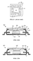
- FIGS. 7 and 8 respectively show a cross-sectional side elevational view and a top plan view of the semiconductor device 400 .
- FIG. 7 is taken along the line A-A in FIG. 8 ; and for clarity, the plurality of leads 18 are also shown in FIG. 7 .
- the semiconductor device 400 is obtained from a combination of the semiconductor device 200 shown in FIGS. 3 and 4 , and the semiconductor device 300 shown in FIGS. 5 and 6 , and provides an even higher heat dissipation efficiency.
- the portion 25 of the exposed segment of the tie bar 24 that is in contact with the top surface 12 a of the package body 12 is received within a groove 34 of the top surface 12 a of the package body 12 to ensure a flat profile of the structure.
- a thermally conductive member 26 is attached to and in contact with both the top surface 12 a of the package body 12 , more particularly, the middle part thereof, and the portion 25 of the exposed segment of the tie bar 24 , which is located at a corner of the top surface 12 a of the package body 12 .
- thermally conductive member 26 provides an integral heat sink together with the tie bar 24 , greatly increasing the thermal dissipation efficiency of the semiconductor device 400 , especially for the top surface 12 a of the package body 12 .
- the thermally conductive member 26 is disposed in a recess 46 of the top surface 12 a of the package body 12 , as in the semiconductor device 200 .
- the depth of the groove 34 for accommodating the portion 25 of the exposed segment of each tie bar 24 is larger than that of the recess 46 for accommodating the thermally conductive member 26 so that the top surface of the portion 25 of the exposed segment of the tie bar 24 is level with the bottom surface of the recess 46 , thereby the thermally conductive member 26 is in contact with both the top surface 12 a of the package body 12 and the portion 25 of the exposed segment of the tie bar 24 .
- the top surface of the thermally conductive member 26 can be lower or higher than the top surface 12 a of the package body 12 outside the recess 46 , or the top surface of the thermally conductive member 26 and the top surface 12 a of the package body 12 outside the recess 46 are level with each other.
- the thermally conductive member 26 is preferably made from a material with good heat conductance, as in the semiconductor device 200 .
- the thermally conductive member 26 is a metal member, though it is not necessarily limited thereto.
- the thermally conductive member 26 comprises a metal slug, as in the semiconductor device 200 .
- the metal slug is preferably fixedly attached to the portion 25 of the exposed segment of the tie bar 24 with a solder 50 , though it is not necessarily limited thereto.
- the thermally conductive member 26 comprises melted solder reflow in the recess 46 , as in the semiconductor device 200 .
- the top surface of the portion 25 of the exposed segment of each tie bar 24 is not necessarily level with the bottom surface of the recess 46 .
- the thermally conductive member 26 is still in contact with both the top surface 12 a of the package body 12 (in the recess 46 ) and the portion 25 of the exposed segment of the tie bar 24 due to the flowability of the solder paste.
- the tie bar 24 is typically made of metals such as copper (Cu), aluminium (Al) or the like, the metal slug formed from the solder paste reflow may be fixedly attached to the portion 25 of the exposed segment of the tie bar 24 so as to be integral without any further processing.
- the thermally conductive member 26 has a general shape of a square. However, any other appropriate shapes may be used as well.
- the size of the thermally conductive member 26 is not particularly limited. It is preferred that the thermally conductive member 26 covers both the active surface 16 a of the semiconductor die 16 and the top surface of the portion 25 of the exposed segment of each tie bar 24 , which ensures better results of heat conduction and dissipation.
- the thickness of the thermally conductive member 26 is not particularly limited either, and it is varied as necessary depending on the configurations of the semiconductor die 16 , the PCB 14 and the package body 12 , or other like factors.
- FIG. 10A a schematic cross sectional view of a semiconductor device 500 in accordance with an embodiment of the present invention is shown. Similar to the semiconductor device 400 shown in FIG. 7 , the tie bar 24 in the semiconductor device 500 has an exposed segment extending from the die flag 22 along the bottom surface 12 b of the package body 12 , up the side surface 12 c of the package body 12 , and onto the top surface 12 a of the package body 12 . The portion 25 of the exposed segment is attached to the top surface 12 a of the package body 12 . A T-shaped thermally conductive member 502 is attached to the top surface 12 a of the package body 12 .
- the package body 12 has a central cavity 504 within which a base 506 of the T-shaped thermally conductive member 502 is received and attached.
- the T-shaped thermally conductive member 502 also has at least one notch 508 formed at an inner end of the “T” section that receive and contact the portion 25 of the tie bar 24 .
- FIG. 10B shows a schematic cross sectional view of a semiconductor device 600 in accordance with another embodiment of the present invention.
- the semiconductor device 600 is similar to the semiconductor device 500 shown in FIG. 10A except that the notch 604 is formed in the top surface 12 a of the package body 12 to receive the portion 25 of the tie bar 24 and then the T-shaped thermally conductive member 602 does not need notches to accommodate the tie bar 24 .
- FIG. 11 is a flow chart showing the steps of a method 4000 of assembling the semiconductor device 400 with reference to FIGS. 7, 8 and 9 .
- the method 4000 starts at S 205 by electrically connecting a semiconductor die 16 to each of a plurality of leads 18 of a lead frame 40 preferably with a bonding wire 20 .
- the semiconductor die 16 is encapsulated in a packaging material to form a package body 12 , wherein the package body has a top surface 12 a and an opposing bottom surface 12 b , and the semiconductor die 16 has an active surface 16 a facing the top surface 12 a of the package body 12 and an opposing bottom surface 16 b facing the bottom surface 12 b of the package body 12 .
- a portion of each of the plurality of leads 18 and the bonding wire 20 are also encapsulated in the packaging material to form the package body 12 at the same time.
- At least one tie bar 24 is partially encapsulated within the package body 12 and has an exposed segment extending outside of the package body 12 .
- the leads 18 and the tie bar 24 are severed from the support 44 of the lead frame 40 preferably by sawing or punching, or other known singulation process.
- the singulation process also provides the opportunity to shape a portion 25 of the exposed segment of the tie bar 24 as desired.
- the severing and shaping occurs simultaneously or successively.
- the exposed segment of the tie bar 24 is bent over the package body 12 , wherein the portion 25 of the exposed segment is in contact with the top surface 12 a of the package body 12 .
- an adhesive such as thermal glue is applied for fixed attachment prior to or following the bending process.
- the portion 25 is received within a groove 34 formed in the top surface 12 a of the package body 12 . Similar to the recess 46 , the groove 34 is preferably formed by a mold chase that has a convex portion during the encapsulation process, or is formed at any time following the encapsulation process by etching or the like.
- a thermally conductive member 26 is disposed on the top surface 12 a of the package body 12 , wherein the thermally conductive member 26 is in contact with the top surface 12 a of the package body 12 and a top surface of the portion 25 of the exposed segment of the tie bar 24 , and spaced from the active surface 16 a of the semiconductor die 16 by the packaging material. Therefore, the thermally conductive member 26 , together with the tie bar 24 , forms an integral heat sink to conduct heat generated by the semiconductor die 16 , especially from the top surface 12 a of the package body 12 .
- the thermally conductive member 26 is disposed and accommodated in the recess 46 of the top surface 12 a of the package body 12 .
- the thermally conductive member 26 comprises a metal slug disposed directly on the top surface 12 a of the package body 12 or disposed in the recess 46 of the top surface 12 a of the package body 12 .
- Solder 50 is preferably applied for fixedly attaching the metal slug to the portion 25 of the exposed segment of each tie bar 24 .
- the thermally conductive member 26 comprises melted solder and disposing the thermally conductive member 26 within the recess 46 comprises reflowing the solder.
- the word ‘comprising’ or ‘having’ does not exclude the presence of other elements or steps than those listed in a claim.
- the term “a” or “an”, as used herein, is defined as one or more than one.
- the use of introductory phrases such as “at least one” and “one or more” in the claims should not be construed to imply that the introduction of another claim element by the indefinite articles “a” or “an” limits any particular claim containing such introduced claim element to inventions containing only one such element, even when the same claim includes the introductory phrases “one or more” or “at least one” and indefinite articles such as “a” or “an”. The same holds true for the use of definite articles.
Abstract
Description
Claims (12)
Applications Claiming Priority (3)
| Application Number | Priority Date | Filing Date | Title |
|---|---|---|---|
| CN201310489288.9A CN104576565A (en) | 2013-10-18 | 2013-10-18 | Semiconductor device provided with radiator and assembly method of semiconductor device |
| CN201310489288 | 2013-10-18 | ||
| CN201310489288.9 | 2013-10-18 |
Publications (2)
| Publication Number | Publication Date |
|---|---|
| US20150108625A1 US20150108625A1 (en) | 2015-04-23 |
| US9484289B2 true US9484289B2 (en) | 2016-11-01 |
Family
ID=52825478
Family Applications (1)
| Application Number | Title | Priority Date | Filing Date |
|---|---|---|---|
| US14/462,567 Active 2034-09-12 US9484289B2 (en) | 2013-10-18 | 2014-08-19 | Semiconductor device with heat spreader |
Country Status (2)
| Country | Link |
|---|---|
| US (1) | US9484289B2 (en) |
| CN (1) | CN104576565A (en) |
Cited By (1)
| Publication number | Priority date | Publication date | Assignee | Title |
|---|---|---|---|---|
| US11049817B2 (en) * | 2019-02-25 | 2021-06-29 | Nxp B.V. | Semiconductor device with integral EMI shield |
Families Citing this family (4)
| Publication number | Priority date | Publication date | Assignee | Title |
|---|---|---|---|---|
| JPWO2014188632A1 (en) * | 2013-05-23 | 2017-02-23 | パナソニック株式会社 | Semiconductor device having heat dissipation structure and laminated body of semiconductor device |
| US9953904B1 (en) | 2016-10-25 | 2018-04-24 | Nxp Usa, Inc. | Electronic component package with heatsink and multiple electronic components |
| KR102603421B1 (en) | 2019-01-22 | 2023-11-17 | 양쯔 메모리 테크놀로지스 씨오., 엘티디. | Integrated circuit packaging structure and manufacturing method thereof |
| US11121094B2 (en) * | 2019-06-20 | 2021-09-14 | Amkor Technology Singapore Holding Pte. Ltd. | Semiconductor devices with shield |
Citations (26)
| Publication number | Priority date | Publication date | Assignee | Title |
|---|---|---|---|---|
| US3930114A (en) | 1975-03-17 | 1975-12-30 | Nat Semiconductor Corp | Integrated circuit package utilizing novel heat sink structure |
| US5041902A (en) | 1989-12-14 | 1991-08-20 | Motorola, Inc. | Molded electronic package with compression structures |
| US5072283A (en) | 1988-04-12 | 1991-12-10 | Bolger Justin C | Pre-formed chip carrier cavity package |
| US5559306A (en) * | 1994-05-17 | 1996-09-24 | Olin Corporation | Electronic package with improved electrical performance |
| US5629561A (en) * | 1994-12-16 | 1997-05-13 | Anam Industrial Co., Ltd. | Semiconductor package with integral heat dissipator |
| US5679975A (en) | 1995-12-18 | 1997-10-21 | Integrated Device Technology, Inc. | Conductive encapsulating shield for an integrated circuit |
| US5723899A (en) | 1994-08-30 | 1998-03-03 | Amkor Electronics, Inc. | Semiconductor lead frame having connection bar and guide rings |
| US6222258B1 (en) * | 1996-11-11 | 2001-04-24 | Fujitsu Limited | Semiconductor device and method for producing a semiconductor device |
| US6265771B1 (en) * | 1999-01-27 | 2001-07-24 | International Business Machines Corporation | Dual chip with heat sink |
| US6329705B1 (en) * | 1998-05-20 | 2001-12-11 | Micron Technology, Inc. | Leadframes including offsets extending from a major plane thereof, packaged semiconductor devices including same, and method of designing and fabricating such leadframes |
| US6369455B1 (en) * | 2000-01-04 | 2002-04-09 | Siliconware Precision Industries Co., Ltd. | Externally-embedded heat-dissipating device for ball grid array integrated circuit package |
| US6469380B2 (en) * | 2000-11-08 | 2002-10-22 | Citizen Watch Co., Ltd. | Resin sealed semiconductor device utilizing a clad material heat sink |
| US20030160313A1 (en) | 2002-02-28 | 2003-08-28 | Mitsubishi Denki Kabushiki Kaisha | Semiconductor device |
| US6918178B2 (en) | 2000-04-08 | 2005-07-19 | Advanced Semiconductor Engineering, Inc. | Method of attaching a heat sink to an IC package |
| US7009283B1 (en) | 1999-04-14 | 2006-03-07 | Amkor Technology, Inc. | Nonexposed heat sink for semiconductor package |
| US20070090502A1 (en) * | 2005-10-20 | 2007-04-26 | Broadcom Corporation | Methods and apparatus for improved thermal performance and electromagnetic interference (EMI) shielding in leadframe integrated circuit (IC) packages |
| US20070132091A1 (en) * | 2005-12-09 | 2007-06-14 | Chung-Lin Wu | Thermal enhanced upper and dual heat sink exposed molded leadless package |
| US20070284733A1 (en) * | 2006-06-08 | 2007-12-13 | Advanced Interconnect Technologies Limited, A Corporation Of Mauritius. | Method of making thermally enhanced substrate-base package |
| US7479692B2 (en) * | 2006-11-09 | 2009-01-20 | Stats Chippac Ltd. | Integrated circuit package system with heat sink |
| US7545032B2 (en) * | 2006-07-10 | 2009-06-09 | Stats Chippac Ltd. | Integrated circuit package system with stiffener |
| US20090146269A1 (en) * | 2007-12-07 | 2009-06-11 | Seng Guan Chow | Integrated circuit package system with shield |
| US7598903B2 (en) * | 2006-05-23 | 2009-10-06 | Korea Advanced Institute Of Science And Technology | Sensor for measuring distance and method for measuring distance using the sensor |
| US7902644B2 (en) | 2007-12-07 | 2011-03-08 | Stats Chippac Ltd. | Integrated circuit package system for electromagnetic isolation |
| US8211753B2 (en) * | 2003-08-26 | 2012-07-03 | Stats Chippac Ltd. | Leadframe-based mold array package heat spreader and fabrication method therefor |
| US20140103505A1 (en) * | 2012-10-16 | 2014-04-17 | Broadcom Corporation | Die down integrated circuit package with integrated heat spreader and leads |
| US8901722B2 (en) | 2013-02-27 | 2014-12-02 | Freescale Semiconductor, Inc. | Semiconductor device with integral heat sink |
Family Cites Families (2)
| Publication number | Priority date | Publication date | Assignee | Title |
|---|---|---|---|---|
| JPH07283352A (en) * | 1994-04-11 | 1995-10-27 | Fujitsu Ltd | Semiconductor device and its carrying method |
| JP2008187101A (en) * | 2007-01-31 | 2008-08-14 | Yamaha Corp | Semiconductor device and mounting structure of semiconductor device |
-
2013
- 2013-10-18 CN CN201310489288.9A patent/CN104576565A/en active Pending
-
2014
- 2014-08-19 US US14/462,567 patent/US9484289B2/en active Active
Patent Citations (26)
| Publication number | Priority date | Publication date | Assignee | Title |
|---|---|---|---|---|
| US3930114A (en) | 1975-03-17 | 1975-12-30 | Nat Semiconductor Corp | Integrated circuit package utilizing novel heat sink structure |
| US5072283A (en) | 1988-04-12 | 1991-12-10 | Bolger Justin C | Pre-formed chip carrier cavity package |
| US5041902A (en) | 1989-12-14 | 1991-08-20 | Motorola, Inc. | Molded electronic package with compression structures |
| US5559306A (en) * | 1994-05-17 | 1996-09-24 | Olin Corporation | Electronic package with improved electrical performance |
| US5723899A (en) | 1994-08-30 | 1998-03-03 | Amkor Electronics, Inc. | Semiconductor lead frame having connection bar and guide rings |
| US5629561A (en) * | 1994-12-16 | 1997-05-13 | Anam Industrial Co., Ltd. | Semiconductor package with integral heat dissipator |
| US5679975A (en) | 1995-12-18 | 1997-10-21 | Integrated Device Technology, Inc. | Conductive encapsulating shield for an integrated circuit |
| US6222258B1 (en) * | 1996-11-11 | 2001-04-24 | Fujitsu Limited | Semiconductor device and method for producing a semiconductor device |
| US6329705B1 (en) * | 1998-05-20 | 2001-12-11 | Micron Technology, Inc. | Leadframes including offsets extending from a major plane thereof, packaged semiconductor devices including same, and method of designing and fabricating such leadframes |
| US6265771B1 (en) * | 1999-01-27 | 2001-07-24 | International Business Machines Corporation | Dual chip with heat sink |
| US7009283B1 (en) | 1999-04-14 | 2006-03-07 | Amkor Technology, Inc. | Nonexposed heat sink for semiconductor package |
| US6369455B1 (en) * | 2000-01-04 | 2002-04-09 | Siliconware Precision Industries Co., Ltd. | Externally-embedded heat-dissipating device for ball grid array integrated circuit package |
| US6918178B2 (en) | 2000-04-08 | 2005-07-19 | Advanced Semiconductor Engineering, Inc. | Method of attaching a heat sink to an IC package |
| US6469380B2 (en) * | 2000-11-08 | 2002-10-22 | Citizen Watch Co., Ltd. | Resin sealed semiconductor device utilizing a clad material heat sink |
| US20030160313A1 (en) | 2002-02-28 | 2003-08-28 | Mitsubishi Denki Kabushiki Kaisha | Semiconductor device |
| US8211753B2 (en) * | 2003-08-26 | 2012-07-03 | Stats Chippac Ltd. | Leadframe-based mold array package heat spreader and fabrication method therefor |
| US20070090502A1 (en) * | 2005-10-20 | 2007-04-26 | Broadcom Corporation | Methods and apparatus for improved thermal performance and electromagnetic interference (EMI) shielding in leadframe integrated circuit (IC) packages |
| US20070132091A1 (en) * | 2005-12-09 | 2007-06-14 | Chung-Lin Wu | Thermal enhanced upper and dual heat sink exposed molded leadless package |
| US7598903B2 (en) * | 2006-05-23 | 2009-10-06 | Korea Advanced Institute Of Science And Technology | Sensor for measuring distance and method for measuring distance using the sensor |
| US20070284733A1 (en) * | 2006-06-08 | 2007-12-13 | Advanced Interconnect Technologies Limited, A Corporation Of Mauritius. | Method of making thermally enhanced substrate-base package |
| US7545032B2 (en) * | 2006-07-10 | 2009-06-09 | Stats Chippac Ltd. | Integrated circuit package system with stiffener |
| US7479692B2 (en) * | 2006-11-09 | 2009-01-20 | Stats Chippac Ltd. | Integrated circuit package system with heat sink |
| US20090146269A1 (en) * | 2007-12-07 | 2009-06-11 | Seng Guan Chow | Integrated circuit package system with shield |
| US7902644B2 (en) | 2007-12-07 | 2011-03-08 | Stats Chippac Ltd. | Integrated circuit package system for electromagnetic isolation |
| US20140103505A1 (en) * | 2012-10-16 | 2014-04-17 | Broadcom Corporation | Die down integrated circuit package with integrated heat spreader and leads |
| US8901722B2 (en) | 2013-02-27 | 2014-12-02 | Freescale Semiconductor, Inc. | Semiconductor device with integral heat sink |
Non-Patent Citations (1)
| Title |
|---|
| Notice of Allowance dated Oct. 15, 2014 in U.S. Appl. No. 14/077205. |
Cited By (1)
| Publication number | Priority date | Publication date | Assignee | Title |
|---|---|---|---|---|
| US11049817B2 (en) * | 2019-02-25 | 2021-06-29 | Nxp B.V. | Semiconductor device with integral EMI shield |
Also Published As
| Publication number | Publication date |
|---|---|
| US20150108625A1 (en) | 2015-04-23 |
| CN104576565A (en) | 2015-04-29 |
Similar Documents
| Publication | Publication Date | Title |
|---|---|---|
| KR101539250B1 (en) | Thermally enhanced thin semiconductor package | |
| US7582958B2 (en) | Semiconductor package | |
| US9484289B2 (en) | Semiconductor device with heat spreader | |
| TW200913201A (en) | Dual side cooling integrated power device package and module and methods of manufacture | |
| US7402459B2 (en) | Quad flat no-lead (QFN) chip package assembly apparatus and method | |
| US20160240452A1 (en) | Semiconductor packages with sub-terminals and related methods | |
| JP2007184501A (en) | Resin-sealed semiconductor device with externally exposed radiators at its top, and method for fabrication thereof | |
| US9961798B2 (en) | Package and a method of manufacturing the same | |
| JP2012199436A (en) | Semiconductor device and manufacturing method of the same | |
| US8901722B2 (en) | Semiconductor device with integral heat sink | |
| US9666557B2 (en) | Small footprint semiconductor package | |
| KR20170092112A (en) | Resin-encapsulated semiconductor device | |
| US7566967B2 (en) | Semiconductor package structure for vertical mount and method | |
| JP6150866B2 (en) | Power semiconductor device | |
| US9613941B2 (en) | Exposed die power semiconductor device | |
| JP2016162964A (en) | Semiconductor device manufacturing method and semiconductor device | |
| TWI393227B (en) | Packaged integrated circuits and methods to form a stacked integrated circuit package | |
| US9209119B1 (en) | Semiconductor device assembled using two lead frames | |
| US8120169B2 (en) | Thermally enhanced molded leadless package | |
| US10840172B2 (en) | Leadframe, semiconductor package including a leadframe and method for forming a semiconductor package | |
| JP4207791B2 (en) | Semiconductor device | |
| JP6065500B2 (en) | Semiconductor device | |
| KR19980084769A (en) | High heat dissipation package and its manufacturing method | |
| JP2001352008A (en) | Semiconductor device and its manufacturing method | |
| JP2006294740A (en) | Electronic device |
Legal Events
| Date | Code | Title | Description |
|---|---|---|---|
| AS | Assignment |
Owner name: FREESCALE SEMICONDUCTOR, INC., TEXAS Free format text: ASSIGNMENT OF ASSIGNORS INTEREST;ASSIGNORS:GE, YOU;LYE, MENG KONG;MEI, PENGLIN;SIGNING DATES FROM 20130919 TO 20130920;REEL/FRAME:033557/0848 |
|
| AS | Assignment |
Owner name: CITIBANK, N.A., AS NOTES COLLATERAL AGENT, NEW YORK Free format text: SUPPLEMENT TO IP SECURITY AGREEMENT;ASSIGNOR:FREESCALE SEMICONDUCTOR, INC.;REEL/FRAME:034160/0370 Effective date: 20141030 Owner name: CITIBANK, N.A., AS NOTES COLLATERAL AGENT, NEW YORK Free format text: SUPPLEMENT TO IP SECURITY AGREEMENT;ASSIGNOR:FREESCALE SEMICONDUCTOR, INC.;REEL/FRAME:034160/0351 Effective date: 20141030 Owner name: CITIBANK, N.A., AS NOTES COLLATERAL AGENT, NEW YORK Free format text: SUPPLEMENT TO IP SECURITY AGREEMENT;ASSIGNOR:FREESCALE SEMICONDUCTOR, INC.;REEL/FRAME:034153/0027 Effective date: 20141030 Owner name: CITIBANK, N.A., AS NOTES COLLATERAL AGENT, NEW YOR Free format text: SUPPLEMENT TO IP SECURITY AGREEMENT;ASSIGNOR:FREESCALE SEMICONDUCTOR, INC.;REEL/FRAME:034153/0027 Effective date: 20141030 Owner name: CITIBANK, N.A., AS NOTES COLLATERAL AGENT, NEW YOR Free format text: SUPPLEMENT TO IP SECURITY AGREEMENT;ASSIGNOR:FREESCALE SEMICONDUCTOR, INC.;REEL/FRAME:034160/0351 Effective date: 20141030 Owner name: CITIBANK, N.A., AS NOTES COLLATERAL AGENT, NEW YOR Free format text: SUPPLEMENT TO IP SECURITY AGREEMENT;ASSIGNOR:FREESCALE SEMICONDUCTOR, INC.;REEL/FRAME:034160/0370 Effective date: 20141030 |
|
| AS | Assignment |
Owner name: FREESCALE SEMICONDUCTOR, INC., TEXAS Free format text: PATENT RELEASE;ASSIGNOR:CITIBANK, N.A., AS COLLATERAL AGENT;REEL/FRAME:037357/0921 Effective date: 20151207 |
|
| AS | Assignment |
Owner name: MORGAN STANLEY SENIOR FUNDING, INC., MARYLAND Free format text: ASSIGNMENT AND ASSUMPTION OF SECURITY INTEREST IN PATENTS;ASSIGNOR:CITIBANK, N.A.;REEL/FRAME:037458/0460 Effective date: 20151207 Owner name: MORGAN STANLEY SENIOR FUNDING, INC., MARYLAND Free format text: ASSIGNMENT AND ASSUMPTION OF SECURITY INTEREST IN PATENTS;ASSIGNOR:CITIBANK, N.A.;REEL/FRAME:037458/0502 Effective date: 20151207 |
|
| AS | Assignment |
Owner name: MORGAN STANLEY SENIOR FUNDING, INC., MARYLAND Free format text: SECURITY AGREEMENT SUPPLEMENT;ASSIGNOR:NXP B.V.;REEL/FRAME:038017/0058 Effective date: 20160218 |
|
| AS | Assignment |
Owner name: MORGAN STANLEY SENIOR FUNDING, INC., MARYLAND Free format text: SUPPLEMENT TO THE SECURITY AGREEMENT;ASSIGNOR:FREESCALE SEMICONDUCTOR, INC.;REEL/FRAME:039138/0001 Effective date: 20160525 |
|
| AS | Assignment |
Owner name: MORGAN STANLEY SENIOR FUNDING, INC., MARYLAND Free format text: CORRECTIVE ASSIGNMENT TO CORRECT THE REMOVE APPLICATION 12092129 PREVIOUSLY RECORDED ON REEL 038017 FRAME 0058. ASSIGNOR(S) HEREBY CONFIRMS THE SECURITY AGREEMENT SUPPLEMENT;ASSIGNOR:NXP B.V.;REEL/FRAME:039361/0212 Effective date: 20160218 |
|
| AS | Assignment |
Owner name: NXP, B.V., F/K/A FREESCALE SEMICONDUCTOR, INC., NETHERLANDS Free format text: RELEASE BY SECURED PARTY;ASSIGNOR:MORGAN STANLEY SENIOR FUNDING, INC.;REEL/FRAME:040925/0001 Effective date: 20160912 Owner name: NXP, B.V., F/K/A FREESCALE SEMICONDUCTOR, INC., NE Free format text: RELEASE BY SECURED PARTY;ASSIGNOR:MORGAN STANLEY SENIOR FUNDING, INC.;REEL/FRAME:040925/0001 Effective date: 20160912 |
|
| STCF | Information on status: patent grant |
Free format text: PATENTED CASE |
|
| AS | Assignment |
Owner name: NXP B.V., NETHERLANDS Free format text: RELEASE BY SECURED PARTY;ASSIGNOR:MORGAN STANLEY SENIOR FUNDING, INC.;REEL/FRAME:040928/0001 Effective date: 20160622 |
|
| AS | Assignment |
Owner name: NXP USA, INC., TEXAS Free format text: CHANGE OF NAME;ASSIGNOR:FREESCALE SEMICONDUCTOR, INC.;REEL/FRAME:040632/0001 Effective date: 20161107 |
|
| AS | Assignment |
Owner name: MORGAN STANLEY SENIOR FUNDING, INC., MARYLAND Free format text: CORRECTIVE ASSIGNMENT TO CORRECT THE REMOVE APPLICATION 12681366 PREVIOUSLY RECORDED ON REEL 039361 FRAME 0212. ASSIGNOR(S) HEREBY CONFIRMS THE SECURITY AGREEMENT SUPPLEMENT;ASSIGNOR:NXP B.V.;REEL/FRAME:042762/0145 Effective date: 20160218 Owner name: MORGAN STANLEY SENIOR FUNDING, INC., MARYLAND Free format text: CORRECTIVE ASSIGNMENT TO CORRECT THE REMOVE APPLICATION 12681366 PREVIOUSLY RECORDED ON REEL 038017 FRAME 0058. ASSIGNOR(S) HEREBY CONFIRMS THE SECURITY AGREEMENT SUPPLEMENT;ASSIGNOR:NXP B.V.;REEL/FRAME:042985/0001 Effective date: 20160218 |
|
| AS | Assignment |
Owner name: NXP USA, INC., TEXAS Free format text: CORRECTIVE ASSIGNMENT TO CORRECT THE NATURE OF CONVEYANCE PREVIOUSLY RECORDED AT REEL: 040632 FRAME: 0001. ASSIGNOR(S) HEREBY CONFIRMS THE MERGER AND CHANGE OF NAME;ASSIGNOR:FREESCALE SEMICONDUCTOR INC.;REEL/FRAME:044209/0047 Effective date: 20161107 |
|
| AS | Assignment |
Owner name: NXP B.V., NETHERLANDS Free format text: RELEASE BY SECURED PARTY;ASSIGNOR:MORGAN STANLEY SENIOR FUNDING, INC.;REEL/FRAME:050744/0097 Effective date: 20190903 Owner name: NXP B.V., NETHERLANDS Free format text: RELEASE BY SECURED PARTY;ASSIGNOR:MORGAN STANLEY SENIOR FUNDING, INC.;REEL/FRAME:050745/0001 Effective date: 20190903 |
|
| AS | Assignment |
Owner name: MORGAN STANLEY SENIOR FUNDING, INC., MARYLAND Free format text: CORRECTIVE ASSIGNMENT TO CORRECT THE REMOVE APPLICATION 12298143 PREVIOUSLY RECORDED ON REEL 042762 FRAME 0145. ASSIGNOR(S) HEREBY CONFIRMS THE SECURITY AGREEMENT SUPPLEMENT;ASSIGNOR:NXP B.V.;REEL/FRAME:051145/0184 Effective date: 20160218 Owner name: MORGAN STANLEY SENIOR FUNDING, INC., MARYLAND Free format text: CORRECTIVE ASSIGNMENT TO CORRECT THE REMOVE APPLICATION 12298143 PREVIOUSLY RECORDED ON REEL 039361 FRAME 0212. ASSIGNOR(S) HEREBY CONFIRMS THE SECURITY AGREEMENT SUPPLEMENT;ASSIGNOR:NXP B.V.;REEL/FRAME:051029/0387 Effective date: 20160218 Owner name: MORGAN STANLEY SENIOR FUNDING, INC., MARYLAND Free format text: CORRECTIVE ASSIGNMENT TO CORRECT THE REMOVE APPLICATION 12298143 PREVIOUSLY RECORDED ON REEL 042985 FRAME 0001. ASSIGNOR(S) HEREBY CONFIRMS THE SECURITY AGREEMENT SUPPLEMENT;ASSIGNOR:NXP B.V.;REEL/FRAME:051029/0001 Effective date: 20160218 Owner name: MORGAN STANLEY SENIOR FUNDING, INC., MARYLAND Free format text: CORRECTIVE ASSIGNMENT TO CORRECT THE REMOVE APPLICATION 12298143 PREVIOUSLY RECORDED ON REEL 038017 FRAME 0058. ASSIGNOR(S) HEREBY CONFIRMS THE SECURITY AGREEMENT SUPPLEMENT;ASSIGNOR:NXP B.V.;REEL/FRAME:051030/0001 Effective date: 20160218 Owner name: MORGAN STANLEY SENIOR FUNDING, INC., MARYLAND Free format text: CORRECTIVE ASSIGNMENT TO CORRECT THE REMOVE APPLICATION12298143 PREVIOUSLY RECORDED ON REEL 042985 FRAME 0001. ASSIGNOR(S) HEREBY CONFIRMS THE SECURITY AGREEMENT SUPPLEMENT;ASSIGNOR:NXP B.V.;REEL/FRAME:051029/0001 Effective date: 20160218 Owner name: MORGAN STANLEY SENIOR FUNDING, INC., MARYLAND Free format text: CORRECTIVE ASSIGNMENT TO CORRECT THE REMOVE APPLICATION12298143 PREVIOUSLY RECORDED ON REEL 039361 FRAME 0212. ASSIGNOR(S) HEREBY CONFIRMS THE SECURITY AGREEMENT SUPPLEMENT;ASSIGNOR:NXP B.V.;REEL/FRAME:051029/0387 Effective date: 20160218 Owner name: MORGAN STANLEY SENIOR FUNDING, INC., MARYLAND Free format text: CORRECTIVE ASSIGNMENT TO CORRECT THE REMOVE APPLICATION12298143 PREVIOUSLY RECORDED ON REEL 042762 FRAME 0145. ASSIGNOR(S) HEREBY CONFIRMS THE SECURITY AGREEMENT SUPPLEMENT;ASSIGNOR:NXP B.V.;REEL/FRAME:051145/0184 Effective date: 20160218 |
|
| AS | Assignment |
Owner name: NXP B.V., NETHERLANDS Free format text: CORRECTIVE ASSIGNMENT TO CORRECT THE REMOVEAPPLICATION 11759915 AND REPLACE IT WITH APPLICATION11759935 PREVIOUSLY RECORDED ON REEL 040928 FRAME 0001. ASSIGNOR(S) HEREBY CONFIRMS THE RELEASE OF SECURITYINTEREST;ASSIGNOR:MORGAN STANLEY SENIOR FUNDING, INC.;REEL/FRAME:052915/0001 Effective date: 20160622 |
|
| AS | Assignment |
Owner name: NXP, B.V. F/K/A FREESCALE SEMICONDUCTOR, INC., NETHERLANDS Free format text: CORRECTIVE ASSIGNMENT TO CORRECT THE REMOVEAPPLICATION 11759915 AND REPLACE IT WITH APPLICATION11759935 PREVIOUSLY RECORDED ON REEL 040925 FRAME 0001. ASSIGNOR(S) HEREBY CONFIRMS THE RELEASE OF SECURITYINTEREST;ASSIGNOR:MORGAN STANLEY SENIOR FUNDING, INC.;REEL/FRAME:052917/0001 Effective date: 20160912 |
|
| MAFP | Maintenance fee payment |
Free format text: PAYMENT OF MAINTENANCE FEE, 4TH YEAR, LARGE ENTITY (ORIGINAL EVENT CODE: M1551); ENTITY STATUS OF PATENT OWNER: LARGE ENTITY Year of fee payment: 4 |
|
| MAFP | Maintenance fee payment |
Free format text: PAYMENT OF MAINTENANCE FEE, 8TH YEAR, LARGE ENTITY (ORIGINAL EVENT CODE: M1552); ENTITY STATUS OF PATENT OWNER: LARGE ENTITY Year of fee payment: 8 |