US9482969B2 - Imaging members having electrically and mechanically tuned imaging layers - Google Patents
Imaging members having electrically and mechanically tuned imaging layers Download PDFInfo
- Publication number
- US9482969B2 US9482969B2 US14/638,361 US201514638361A US9482969B2 US 9482969 B2 US9482969 B2 US 9482969B2 US 201514638361 A US201514638361 A US 201514638361A US 9482969 B2 US9482969 B2 US 9482969B2
- Authority
- US
- United States
- Prior art keywords
- charge transport
- imaging member
- transport layer
- layer
- group
- Prior art date
- Legal status (The legal status is an assumption and is not a legal conclusion. Google has not performed a legal analysis and makes no representation as to the accuracy of the status listed.)
- Active
Links
- 238000003384 imaging method Methods 0.000 title claims abstract description 229
- 239000011230 binding agent Substances 0.000 claims abstract description 124
- 229920000642 polymer Polymers 0.000 claims abstract description 109
- 229920000515 polycarbonate Polymers 0.000 claims abstract description 76
- 239000004417 polycarbonate Substances 0.000 claims abstract description 76
- 229920000359 diblock copolymer Polymers 0.000 claims abstract description 72
- -1 polysiloxane Polymers 0.000 claims abstract description 53
- 150000001875 compounds Chemical class 0.000 claims abstract description 29
- IISBACLAFKSPIT-UHFFFAOYSA-N bisphenol A Chemical compound C=1C=C(O)C=CC=1C(C)(C)C1=CC=C(O)C=C1 IISBACLAFKSPIT-UHFFFAOYSA-N 0.000 claims abstract description 22
- 229920002959 polymer blend Polymers 0.000 claims abstract description 21
- 229920005604 random copolymer Polymers 0.000 claims abstract description 20
- 229930185605 Bisphenol Natural products 0.000 claims abstract description 13
- 239000000758 substrate Substances 0.000 claims description 80
- 239000000463 material Substances 0.000 claims description 53
- 239000000203 mixture Substances 0.000 claims description 53
- 150000007524 organic acids Chemical class 0.000 claims description 40
- 125000003118 aryl group Chemical group 0.000 claims description 30
- 229920001577 copolymer Polymers 0.000 claims description 27
- KPUWHANPEXNPJT-UHFFFAOYSA-N disiloxane Chemical class [SiH3]O[SiH3] KPUWHANPEXNPJT-UHFFFAOYSA-N 0.000 claims description 16
- 125000001931 aliphatic group Chemical group 0.000 claims description 14
- 125000002947 alkylene group Chemical group 0.000 claims description 14
- 125000001997 phenyl group Chemical group [H]C1=C([H])C([H])=C(*)C([H])=C1[H] 0.000 claims description 14
- 229920000578 graft copolymer Polymers 0.000 claims description 12
- 238000004140 cleaning Methods 0.000 claims description 10
- SDDLEVPIDBLVHC-UHFFFAOYSA-N Bisphenol Z Chemical class C1=CC(O)=CC=C1C1(C=2C=CC(O)=CC=2)CCCCC1 SDDLEVPIDBLVHC-UHFFFAOYSA-N 0.000 claims description 9
- OFOBLEOULBTSOW-UHFFFAOYSA-N Malonic acid Chemical compound OC(=O)CC(O)=O OFOBLEOULBTSOW-UHFFFAOYSA-N 0.000 claims description 9
- 210000000988 bone and bone Anatomy 0.000 claims description 9
- 238000012986 modification Methods 0.000 claims description 8
- 230000004048 modification Effects 0.000 claims description 8
- 238000011161 development Methods 0.000 claims description 7
- 239000004205 dimethyl polysiloxane Substances 0.000 claims description 7
- 235000013870 dimethyl polysiloxane Nutrition 0.000 claims description 7
- 229920000435 poly(dimethylsiloxane) Polymers 0.000 claims description 7
- 238000012546 transfer Methods 0.000 claims description 6
- 239000000654 additive Substances 0.000 claims description 5
- XLYOFNOQVPJJNP-UHFFFAOYSA-N water Substances O XLYOFNOQVPJJNP-UHFFFAOYSA-N 0.000 claims description 5
- 229920002635 polyurethane Polymers 0.000 claims description 4
- 239000004814 polyurethane Substances 0.000 claims description 4
- 230000035939 shock Effects 0.000 claims description 4
- 125000005587 carbonate group Chemical group 0.000 claims description 3
- 239000003638 chemical reducing agent Substances 0.000 claims description 3
- 239000011256 inorganic filler Substances 0.000 claims description 3
- 238000005259 measurement Methods 0.000 claims description 3
- 239000012766 organic filler Substances 0.000 claims description 3
- 239000002390 adhesive tape Substances 0.000 claims description 2
- 238000009736 wetting Methods 0.000 claims description 2
- 230000007423 decrease Effects 0.000 claims 2
- 229920001296 polysiloxane Polymers 0.000 abstract description 12
- 230000009467 reduction Effects 0.000 abstract description 10
- 239000010410 layer Substances 0.000 description 374
- 238000000576 coating method Methods 0.000 description 46
- 239000011248 coating agent Substances 0.000 description 45
- 230000000903 blocking effect Effects 0.000 description 35
- YMWUJEATGCHHMB-UHFFFAOYSA-N Dichloromethane Chemical compound ClCCl YMWUJEATGCHHMB-UHFFFAOYSA-N 0.000 description 30
- 229920000402 bisphenol A polycarbonate polymer Polymers 0.000 description 29
- 238000000034 method Methods 0.000 description 28
- 239000000853 adhesive Substances 0.000 description 23
- 230000001070 adhesive effect Effects 0.000 description 23
- 239000000243 solution Substances 0.000 description 21
- 239000002245 particle Substances 0.000 description 20
- 239000006185 dispersion Substances 0.000 description 18
- 238000002156 mixing Methods 0.000 description 17
- 239000000126 substance Substances 0.000 description 17
- OGGKVJMNFFSDEV-UHFFFAOYSA-N 3-methyl-n-[4-[4-(n-(3-methylphenyl)anilino)phenyl]phenyl]-n-phenylaniline Chemical compound CC1=CC=CC(N(C=2C=CC=CC=2)C=2C=CC(=CC=2)C=2C=CC(=CC=2)N(C=2C=CC=CC=2)C=2C=C(C)C=CC=2)=C1 OGGKVJMNFFSDEV-UHFFFAOYSA-N 0.000 description 16
- 150000001412 amines Chemical class 0.000 description 16
- 230000008569 process Effects 0.000 description 16
- RTAQQCXQSZGOHL-UHFFFAOYSA-N Titanium Chemical compound [Ti] RTAQQCXQSZGOHL-UHFFFAOYSA-N 0.000 description 15
- 238000009472 formulation Methods 0.000 description 14
- 229910052751 metal Inorganic materials 0.000 description 12
- 239000002184 metal Substances 0.000 description 12
- XNGIFLGASWRNHJ-UHFFFAOYSA-N phthalic acid Chemical compound OC(=O)C1=CC=CC=C1C(O)=O XNGIFLGASWRNHJ-UHFFFAOYSA-N 0.000 description 12
- 230000000694 effects Effects 0.000 description 11
- 239000000123 paper Substances 0.000 description 11
- 238000006116 polymerization reaction Methods 0.000 description 11
- 239000002904 solvent Substances 0.000 description 11
- 229910052719 titanium Inorganic materials 0.000 description 11
- 239000010936 titanium Substances 0.000 description 11
- WYURNTSHIVDZCO-UHFFFAOYSA-N Tetrahydrofuran Chemical compound C1CCOC1 WYURNTSHIVDZCO-UHFFFAOYSA-N 0.000 description 10
- 125000002496 methyl group Chemical group [H]C([H])([H])* 0.000 description 10
- PXHVJJICTQNCMI-UHFFFAOYSA-N Nickel Chemical compound [Ni] PXHVJJICTQNCMI-UHFFFAOYSA-N 0.000 description 8
- 239000012790 adhesive layer Substances 0.000 description 8
- 239000011247 coating layer Substances 0.000 description 8
- 238000013461 design Methods 0.000 description 8
- 108091008695 photoreceptors Proteins 0.000 description 8
- 229920000728 polyester Polymers 0.000 description 8
- VYPSYNLAJGMNEJ-UHFFFAOYSA-N Silicium dioxide Chemical compound O=[Si]=O VYPSYNLAJGMNEJ-UHFFFAOYSA-N 0.000 description 7
- 125000004432 carbon atom Chemical group C* 0.000 description 7
- 230000008602 contraction Effects 0.000 description 7
- 238000002360 preparation method Methods 0.000 description 7
- 229920005989 resin Polymers 0.000 description 7
- 239000011347 resin Substances 0.000 description 7
- BVKZGUZCCUSVTD-UHFFFAOYSA-L Carbonate Chemical compound [O-]C([O-])=O BVKZGUZCCUSVTD-UHFFFAOYSA-L 0.000 description 6
- IEQIEDJGQAUEQZ-UHFFFAOYSA-N phthalocyanine Chemical compound N1C(N=C2C3=CC=CC=C3C(N=C3C4=CC=CC=C4C(=N4)N3)=N2)=C(C=CC=C2)C2=C1N=C1C2=CC=CC=C2C4=N1 IEQIEDJGQAUEQZ-UHFFFAOYSA-N 0.000 description 6
- 239000011112 polyethylene naphthalate Substances 0.000 description 6
- 229920005596 polymer binder Polymers 0.000 description 6
- 239000002491 polymer binding agent Substances 0.000 description 6
- 239000006104 solid solution Substances 0.000 description 6
- 229920001169 thermoplastic Polymers 0.000 description 6
- BUGBHKTXTAQXES-UHFFFAOYSA-N Selenium Chemical compound [Se] BUGBHKTXTAQXES-UHFFFAOYSA-N 0.000 description 5
- QCWXUUIWCKQGHC-UHFFFAOYSA-N Zirconium Chemical compound [Zr] QCWXUUIWCKQGHC-UHFFFAOYSA-N 0.000 description 5
- 239000002318 adhesion promoter Substances 0.000 description 5
- 229910052782 aluminium Inorganic materials 0.000 description 5
- XAGFODPZIPBFFR-UHFFFAOYSA-N aluminium Chemical compound [Al] XAGFODPZIPBFFR-UHFFFAOYSA-N 0.000 description 5
- 230000015572 biosynthetic process Effects 0.000 description 5
- 239000004020 conductor Substances 0.000 description 5
- 238000000151 deposition Methods 0.000 description 5
- 238000001035 drying Methods 0.000 description 5
- 238000001125 extrusion Methods 0.000 description 5
- 125000001153 fluoro group Chemical group F* 0.000 description 5
- 238000002347 injection Methods 0.000 description 5
- 239000007924 injection Substances 0.000 description 5
- 239000011159 matrix material Substances 0.000 description 5
- 238000006386 neutralization reaction Methods 0.000 description 5
- 229910052757 nitrogen Inorganic materials 0.000 description 5
- 238000010791 quenching Methods 0.000 description 5
- 230000000171 quenching effect Effects 0.000 description 5
- 229910052814 silicon oxide Inorganic materials 0.000 description 5
- 238000012360 testing method Methods 0.000 description 5
- YLQBMQCUIZJEEH-UHFFFAOYSA-N tetrahydrofuran Natural products C=1C=COC=1 YLQBMQCUIZJEEH-UHFFFAOYSA-N 0.000 description 5
- 229910052726 zirconium Inorganic materials 0.000 description 5
- 125000006273 (C1-C3) alkyl group Chemical group 0.000 description 4
- OKTJSMMVPCPJKN-UHFFFAOYSA-N Carbon Chemical compound [C] OKTJSMMVPCPJKN-UHFFFAOYSA-N 0.000 description 4
- VYZAMTAEIAYCRO-UHFFFAOYSA-N Chromium Chemical compound [Cr] VYZAMTAEIAYCRO-UHFFFAOYSA-N 0.000 description 4
- 229920004142 LEXAN™ Polymers 0.000 description 4
- 239000004418 Lexan Substances 0.000 description 4
- 239000004793 Polystyrene Substances 0.000 description 4
- KKEYFWRCBNTPAC-UHFFFAOYSA-N Terephthalic acid Chemical compound OC(=O)C1=CC=C(C(O)=O)C=C1 KKEYFWRCBNTPAC-UHFFFAOYSA-N 0.000 description 4
- 230000003213 activating effect Effects 0.000 description 4
- 230000008901 benefit Effects 0.000 description 4
- MVPPADPHJFYWMZ-UHFFFAOYSA-N chlorobenzene Chemical compound ClC1=CC=CC=C1 MVPPADPHJFYWMZ-UHFFFAOYSA-N 0.000 description 4
- 229910052804 chromium Inorganic materials 0.000 description 4
- 239000011651 chromium Substances 0.000 description 4
- 230000007547 defect Effects 0.000 description 4
- 230000008021 deposition Effects 0.000 description 4
- 229910002804 graphite Inorganic materials 0.000 description 4
- 239000010439 graphite Substances 0.000 description 4
- 150000002739 metals Chemical class 0.000 description 4
- 229910052759 nickel Inorganic materials 0.000 description 4
- 230000003287 optical effect Effects 0.000 description 4
- 239000000049 pigment Substances 0.000 description 4
- 229920003023 plastic Polymers 0.000 description 4
- 239000004033 plastic Substances 0.000 description 4
- 229920003207 poly(ethylene-2,6-naphthalate) Polymers 0.000 description 4
- 229920002037 poly(vinyl butyral) polymer Polymers 0.000 description 4
- 229920002223 polystyrene Polymers 0.000 description 4
- 125000006413 ring segment Chemical group 0.000 description 4
- 229910052711 selenium Inorganic materials 0.000 description 4
- 239000011669 selenium Substances 0.000 description 4
- 239000004416 thermosoftening plastic Substances 0.000 description 4
- KIIFVSJBFGYDFV-UHFFFAOYSA-N 1h-benzimidazole;perylene Chemical group C1=CC=C2NC=NC2=C1.C1=CC(C2=CC=CC=3C2=C2C=CC=3)=C3C2=CC=CC3=C1 KIIFVSJBFGYDFV-UHFFFAOYSA-N 0.000 description 3
- QTBSBXVTEAMEQO-UHFFFAOYSA-N Acetic acid Chemical compound CC(O)=O QTBSBXVTEAMEQO-UHFFFAOYSA-N 0.000 description 3
- 229920002799 BoPET Polymers 0.000 description 3
- 229920001634 Copolyester Polymers 0.000 description 3
- 239000004952 Polyamide Substances 0.000 description 3
- BLRPTPMANUNPDV-UHFFFAOYSA-N Silane Chemical compound [SiH4] BLRPTPMANUNPDV-UHFFFAOYSA-N 0.000 description 3
- YXFVVABEGXRONW-UHFFFAOYSA-N Toluene Chemical compound CC1=CC=CC=C1 YXFVVABEGXRONW-UHFFFAOYSA-N 0.000 description 3
- 230000005540 biological transmission Effects 0.000 description 3
- 230000015556 catabolic process Effects 0.000 description 3
- 239000000356 contaminant Substances 0.000 description 3
- 238000007796 conventional method Methods 0.000 description 3
- 125000004122 cyclic group Chemical group 0.000 description 3
- 238000006731 degradation reaction Methods 0.000 description 3
- 238000007765 extrusion coating Methods 0.000 description 3
- RAXXELZNTBOGNW-UHFFFAOYSA-N imidazole Natural products C1=CNC=N1 RAXXELZNTBOGNW-UHFFFAOYSA-N 0.000 description 3
- 230000006872 improvement Effects 0.000 description 3
- AMGQUBHHOARCQH-UHFFFAOYSA-N indium;oxotin Chemical compound [In].[Sn]=O AMGQUBHHOARCQH-UHFFFAOYSA-N 0.000 description 3
- 125000001449 isopropyl group Chemical group [H]C([H])([H])C([H])(*)C([H])([H])[H] 0.000 description 3
- 239000005543 nano-size silicon particle Substances 0.000 description 3
- 229920002647 polyamide Polymers 0.000 description 3
- 229920001230 polyarylate Polymers 0.000 description 3
- 229920000139 polyethylene terephthalate Polymers 0.000 description 3
- 239000005020 polyethylene terephthalate Substances 0.000 description 3
- 230000002028 premature Effects 0.000 description 3
- 230000005855 radiation Effects 0.000 description 3
- 229910000077 silane Inorganic materials 0.000 description 3
- 239000002002 slurry Substances 0.000 description 3
- 239000007787 solid Substances 0.000 description 3
- 238000005507 spraying Methods 0.000 description 3
- 229910001220 stainless steel Inorganic materials 0.000 description 3
- 239000010935 stainless steel Substances 0.000 description 3
- QGZKDVFQNNGYKY-UHFFFAOYSA-N Ammonia Chemical compound N QGZKDVFQNNGYKY-UHFFFAOYSA-N 0.000 description 2
- 229910001369 Brass Inorganic materials 0.000 description 2
- XDTMQSROBMDMFD-UHFFFAOYSA-N Cyclohexane Chemical compound C1CCCCC1 XDTMQSROBMDMFD-UHFFFAOYSA-N 0.000 description 2
- ZOKXTWBITQBERF-UHFFFAOYSA-N Molybdenum Chemical compound [Mo] ZOKXTWBITQBERF-UHFFFAOYSA-N 0.000 description 2
- 239000005041 Mylar™ Substances 0.000 description 2
- IMNFDUFMRHMDMM-UHFFFAOYSA-N N-Heptane Chemical compound CCCCCCC IMNFDUFMRHMDMM-UHFFFAOYSA-N 0.000 description 2
- ISWSIDIOOBJBQZ-UHFFFAOYSA-N Phenol Chemical compound OC1=CC=CC=C1 ISWSIDIOOBJBQZ-UHFFFAOYSA-N 0.000 description 2
- 239000004698 Polyethylene Substances 0.000 description 2
- 239000004642 Polyimide Substances 0.000 description 2
- WCUXLLCKKVVCTQ-UHFFFAOYSA-M Potassium chloride Chemical compound [Cl-].[K+] WCUXLLCKKVVCTQ-UHFFFAOYSA-M 0.000 description 2
- 229910001370 Se alloy Inorganic materials 0.000 description 2
- 239000002253 acid Substances 0.000 description 2
- 230000000996 additive effect Effects 0.000 description 2
- WNLRTRBMVRJNCN-UHFFFAOYSA-N adipic acid Chemical compound OC(=O)CCCCC(O)=O WNLRTRBMVRJNCN-UHFFFAOYSA-N 0.000 description 2
- 229920000180 alkyd Polymers 0.000 description 2
- 125000000217 alkyl group Chemical group 0.000 description 2
- 210000003484 anatomy Anatomy 0.000 description 2
- 239000003963 antioxidant agent Substances 0.000 description 2
- 239000004305 biphenyl Substances 0.000 description 2
- 239000010951 brass Substances 0.000 description 2
- 239000003795 chemical substances by application Substances 0.000 description 2
- JHIVVAPYMSGYDF-UHFFFAOYSA-N cyclohexanone Chemical compound O=C1CCCCC1 JHIVVAPYMSGYDF-UHFFFAOYSA-N 0.000 description 2
- 125000000113 cyclohexyl group Chemical group [H]C1([H])C([H])([H])C([H])([H])C([H])(*)C([H])([H])C1([H])[H] 0.000 description 2
- 238000003618 dip coating Methods 0.000 description 2
- 230000009977 dual effect Effects 0.000 description 2
- 239000002355 dual-layer Substances 0.000 description 2
- 230000005670 electromagnetic radiation Effects 0.000 description 2
- 239000003822 epoxy resin Substances 0.000 description 2
- 238000011156 evaluation Methods 0.000 description 2
- 239000007789 gas Substances 0.000 description 2
- 239000011521 glass Substances 0.000 description 2
- 229910052735 hafnium Inorganic materials 0.000 description 2
- VBJZVLUMGGDVMO-UHFFFAOYSA-N hafnium atom Chemical compound [Hf] VBJZVLUMGGDVMO-UHFFFAOYSA-N 0.000 description 2
- LNEPOXFFQSENCJ-UHFFFAOYSA-N haloperidol Chemical compound C1CC(O)(C=2C=CC(Cl)=CC=2)CCN1CCCC(=O)C1=CC=C(F)C=C1 LNEPOXFFQSENCJ-UHFFFAOYSA-N 0.000 description 2
- 238000010438 heat treatment Methods 0.000 description 2
- 229920001519 homopolymer Polymers 0.000 description 2
- 238000005286 illumination Methods 0.000 description 2
- 229910010272 inorganic material Inorganic materials 0.000 description 2
- 239000011147 inorganic material Substances 0.000 description 2
- 239000011810 insulating material Substances 0.000 description 2
- 239000012212 insulator Substances 0.000 description 2
- 230000003993 interaction Effects 0.000 description 2
- QQVIHTHCMHWDBS-UHFFFAOYSA-N isophthalic acid Chemical compound OC(=O)C1=CC=CC(C(O)=O)=C1 QQVIHTHCMHWDBS-UHFFFAOYSA-N 0.000 description 2
- 229920005684 linear copolymer Polymers 0.000 description 2
- 239000007788 liquid Substances 0.000 description 2
- 230000005226 mechanical processes and functions Effects 0.000 description 2
- 229910044991 metal oxide Inorganic materials 0.000 description 2
- 229910052750 molybdenum Inorganic materials 0.000 description 2
- 239000011733 molybdenum Substances 0.000 description 2
- 229910052758 niobium Inorganic materials 0.000 description 2
- 239000010955 niobium Substances 0.000 description 2
- GUCVJGMIXFAOAE-UHFFFAOYSA-N niobium atom Chemical compound [Nb] GUCVJGMIXFAOAE-UHFFFAOYSA-N 0.000 description 2
- BDJRBEYXGGNYIS-UHFFFAOYSA-N nonanedioic acid Chemical compound OC(=O)CCCCCCCC(O)=O BDJRBEYXGGNYIS-UHFFFAOYSA-N 0.000 description 2
- LYRFLYHAGKPMFH-UHFFFAOYSA-N octadecanamide Chemical compound CCCCCCCCCCCCCCCCCC(N)=O LYRFLYHAGKPMFH-UHFFFAOYSA-N 0.000 description 2
- 239000011368 organic material Substances 0.000 description 2
- WLJVNTCWHIRURA-UHFFFAOYSA-N pimelic acid Chemical compound OC(=O)CCCCCC(O)=O WLJVNTCWHIRURA-UHFFFAOYSA-N 0.000 description 2
- 229920002492 poly(sulfone) Polymers 0.000 description 2
- 229920000058 polyacrylate Polymers 0.000 description 2
- 239000004431 polycarbonate resin Substances 0.000 description 2
- 229920000647 polyepoxide Polymers 0.000 description 2
- 229920000573 polyethylene Polymers 0.000 description 2
- 229920002338 polyhydroxyethylmethacrylate Polymers 0.000 description 2
- 229920001721 polyimide Polymers 0.000 description 2
- 125000002924 primary amino group Chemical group [H]N([H])* 0.000 description 2
- DNXIASIHZYFFRO-UHFFFAOYSA-N pyrazoline Chemical compound C1CN=NC1 DNXIASIHZYFFRO-UHFFFAOYSA-N 0.000 description 2
- 238000009877 rendering Methods 0.000 description 2
- YYMBJDOZVAITBP-UHFFFAOYSA-N rubrene Chemical compound C1=CC=CC=C1C(C1=C(C=2C=CC=CC=2)C2=CC=CC=C2C(C=2C=CC=CC=2)=C11)=C(C=CC=C2)C2=C1C1=CC=CC=C1 YYMBJDOZVAITBP-UHFFFAOYSA-N 0.000 description 2
- CXMXRPHRNRROMY-UHFFFAOYSA-N sebacic acid Chemical compound OC(=O)CCCCCCCCC(O)=O CXMXRPHRNRROMY-UHFFFAOYSA-N 0.000 description 2
- 150000004756 silanes Chemical class 0.000 description 2
- 239000011877 solvent mixture Substances 0.000 description 2
- 238000004544 sputter deposition Methods 0.000 description 2
- TYFQFVWCELRYAO-UHFFFAOYSA-N suberic acid Chemical compound OC(=O)CCCCCCC(O)=O TYFQFVWCELRYAO-UHFFFAOYSA-N 0.000 description 2
- 229910052715 tantalum Inorganic materials 0.000 description 2
- GUVRBAGPIYLISA-UHFFFAOYSA-N tantalum atom Chemical compound [Ta] GUVRBAGPIYLISA-UHFFFAOYSA-N 0.000 description 2
- WFKWXMTUELFFGS-UHFFFAOYSA-N tungsten Chemical compound [W] WFKWXMTUELFFGS-UHFFFAOYSA-N 0.000 description 2
- 229910052721 tungsten Inorganic materials 0.000 description 2
- 239000010937 tungsten Substances 0.000 description 2
- 238000001771 vacuum deposition Methods 0.000 description 2
- 229910052720 vanadium Inorganic materials 0.000 description 2
- GPPXJZIENCGNKB-UHFFFAOYSA-N vanadium Chemical compound [V]#[V] GPPXJZIENCGNKB-UHFFFAOYSA-N 0.000 description 2
- 229940117958 vinyl acetate Drugs 0.000 description 2
- 229920002554 vinyl polymer Polymers 0.000 description 2
- 238000003466 welding Methods 0.000 description 2
- WYTZZXDRDKSJID-UHFFFAOYSA-N (3-aminopropyl)triethoxysilane Chemical compound CCO[Si](OCC)(OCC)CCCN WYTZZXDRDKSJID-UHFFFAOYSA-N 0.000 description 1
- RTBFRGCFXZNCOE-UHFFFAOYSA-N 1-methylsulfonylpiperidin-4-one Chemical compound CS(=O)(=O)N1CCC(=O)CC1 RTBFRGCFXZNCOE-UHFFFAOYSA-N 0.000 description 1
- XDOFQFKRPWOURC-UHFFFAOYSA-N 16-methylheptadecanoic acid Chemical compound CC(C)CCCCCCCCCCCCCCC(O)=O XDOFQFKRPWOURC-UHFFFAOYSA-N 0.000 description 1
- OFAPSLLQSSHRSQ-UHFFFAOYSA-N 1H-triazine-2,4-diamine Chemical class NN1NC=CC(N)=N1 OFAPSLLQSSHRSQ-UHFFFAOYSA-N 0.000 description 1
- OEPOKWHJYJXUGD-UHFFFAOYSA-N 2-(3-phenylmethoxyphenyl)-1,3-thiazole-4-carbaldehyde Chemical compound O=CC1=CSC(C=2C=C(OCC=3C=CC=CC=3)C=CC=2)=N1 OEPOKWHJYJXUGD-UHFFFAOYSA-N 0.000 description 1
- OFQCQIGMURIECL-UHFFFAOYSA-N 2-[2-(diethylamino)ethyl]-2',6'-dimethylspiro[isoquinoline-4,4'-oxane]-1,3-dione;phosphoric acid Chemical compound OP(O)(O)=O.O=C1N(CCN(CC)CC)C(=O)C2=CC=CC=C2C21CC(C)OC(C)C2 OFQCQIGMURIECL-UHFFFAOYSA-N 0.000 description 1
- NGXPSFCDNMDGCI-UHFFFAOYSA-N 2-chloro-n-[4-[4-(n-(2-chlorophenyl)anilino)phenyl]phenyl]-n-phenylaniline Chemical compound ClC1=CC=CC=C1N(C=1C=CC(=CC=1)C=1C=CC(=CC=1)N(C=1C=CC=CC=1)C=1C(=CC=CC=1)Cl)C1=CC=CC=C1 NGXPSFCDNMDGCI-UHFFFAOYSA-N 0.000 description 1
- MEPWMMZGWMVZOH-UHFFFAOYSA-N 2-n-trimethoxysilylpropane-1,2-diamine Chemical compound CO[Si](OC)(OC)NC(C)CN MEPWMMZGWMVZOH-UHFFFAOYSA-N 0.000 description 1
- HXLAEGYMDGUSBD-UHFFFAOYSA-N 3-[diethoxy(methyl)silyl]propan-1-amine Chemical compound CCO[Si](C)(OCC)CCCN HXLAEGYMDGUSBD-UHFFFAOYSA-N 0.000 description 1
- SJECZPVISLOESU-UHFFFAOYSA-N 3-trimethoxysilylpropan-1-amine Chemical compound CO[Si](OC)(OC)CCCN SJECZPVISLOESU-UHFFFAOYSA-N 0.000 description 1
- MNFZZNNFORDXSV-UHFFFAOYSA-N 4-(diethylamino)benzaldehyde Chemical compound CCN(CC)C1=CC=C(C=O)C=C1 MNFZZNNFORDXSV-UHFFFAOYSA-N 0.000 description 1
- GAYAMEKFIBYRJW-UHFFFAOYSA-N 4-(fluoren-9-ylidenemethyl)-n,n-dimethylaniline Chemical compound C1=CC(N(C)C)=CC=C1C=C1C2=CC=CC=C2C2=CC=CC=C21 GAYAMEKFIBYRJW-UHFFFAOYSA-N 0.000 description 1
- UZGVMZRBRRYLIP-UHFFFAOYSA-N 4-[5-[4-(diethylamino)phenyl]-1,3,4-oxadiazol-2-yl]-n,n-diethylaniline Chemical compound C1=CC(N(CC)CC)=CC=C1C1=NN=C(C=2C=CC(=CC=2)N(CC)CC)O1 UZGVMZRBRRYLIP-UHFFFAOYSA-N 0.000 description 1
- BMKOVBATNIFKNA-UHFFFAOYSA-N 4-[diethoxy(methyl)silyl]butan-2-amine Chemical compound CCO[Si](C)(OCC)CCC(C)N BMKOVBATNIFKNA-UHFFFAOYSA-N 0.000 description 1
- RLAKMPSLKYFHPL-UHFFFAOYSA-N 4-aminobenzenesulfonic acid;2-dodecylbenzenesulfonic acid;propan-2-ol;titanium Chemical compound [Ti].CC(C)O.NC1=CC=C(S(O)(=O)=O)C=C1.CCCCCCCCCCCCC1=CC=CC=C1S(O)(=O)=O.CCCCCCCCCCCCC1=CC=CC=C1S(O)(=O)=O RLAKMPSLKYFHPL-UHFFFAOYSA-N 0.000 description 1
- GBIDVAHDYHDYFG-UHFFFAOYSA-J 4-aminobenzoate titanium(4+) Chemical compound [Ti+4].Nc1ccc(cc1)C([O-])=O.Nc1ccc(cc1)C([O-])=O.Nc1ccc(cc1)C([O-])=O.Nc1ccc(cc1)C([O-])=O GBIDVAHDYHDYFG-UHFFFAOYSA-J 0.000 description 1
- SRRPHAPPCGRQKB-UHFFFAOYSA-N 4-aminobenzoic acid;16-methylheptadecanoic acid;propan-2-ol;titanium Chemical compound [Ti].CC(C)O.NC1=CC=C(C(O)=O)C=C1.NC1=CC=C(C(O)=O)C=C1.CC(C)CCCCCCCCCCCCCCC(O)=O SRRPHAPPCGRQKB-UHFFFAOYSA-N 0.000 description 1
- OMIHGPLIXGGMJB-UHFFFAOYSA-N 7-oxabicyclo[4.1.0]hepta-1,3,5-triene Chemical compound C1=CC=C2OC2=C1 OMIHGPLIXGGMJB-UHFFFAOYSA-N 0.000 description 1
- 102100026735 Coagulation factor VIII Human genes 0.000 description 1
- RYGMFSIKBFXOCR-UHFFFAOYSA-N Copper Chemical compound [Cu] RYGMFSIKBFXOCR-UHFFFAOYSA-N 0.000 description 1
- UAUDZVJPLUQNMU-UHFFFAOYSA-N Erucasaeureamid Natural products CCCCCCCCC=CCCCCCCCCCCCC(N)=O UAUDZVJPLUQNMU-UHFFFAOYSA-N 0.000 description 1
- LFQSCWFLJHTTHZ-UHFFFAOYSA-N Ethanol Chemical compound CCO LFQSCWFLJHTTHZ-UHFFFAOYSA-N 0.000 description 1
- 239000001856 Ethyl cellulose Substances 0.000 description 1
- ZZSNKZQZMQGXPY-UHFFFAOYSA-N Ethyl cellulose Chemical compound CCOCC1OC(OC)C(OCC)C(OCC)C1OC1C(O)C(O)C(OC)C(CO)O1 ZZSNKZQZMQGXPY-UHFFFAOYSA-N 0.000 description 1
- 101000911390 Homo sapiens Coagulation factor VIII Proteins 0.000 description 1
- WOBHKFSMXKNTIM-UHFFFAOYSA-N Hydroxyethyl methacrylate Chemical compound CC(=C)C(=O)OCCO WOBHKFSMXKNTIM-UHFFFAOYSA-N 0.000 description 1
- 239000004420 Iupilon Substances 0.000 description 1
- 229920000271 Kevlar® Polymers 0.000 description 1
- 229920000305 Nylon 6,10 Polymers 0.000 description 1
- 239000004721 Polyphenylene oxide Substances 0.000 description 1
- 239000004734 Polyphenylene sulfide Substances 0.000 description 1
- 239000004743 Polypropylene Substances 0.000 description 1
- BQCADISMDOOEFD-UHFFFAOYSA-N Silver Chemical compound [Ag] BQCADISMDOOEFD-UHFFFAOYSA-N 0.000 description 1
- 229910000831 Steel Inorganic materials 0.000 description 1
- ATJFFYVFTNAWJD-UHFFFAOYSA-N Tin Chemical compound [Sn] ATJFFYVFTNAWJD-UHFFFAOYSA-N 0.000 description 1
- XTXRWKRVRITETP-UHFFFAOYSA-N Vinyl acetate Chemical compound CC(=O)OC=C XTXRWKRVRITETP-UHFFFAOYSA-N 0.000 description 1
- BZHJMEDXRYGGRV-UHFFFAOYSA-N Vinyl chloride Chemical compound ClC=C BZHJMEDXRYGGRV-UHFFFAOYSA-N 0.000 description 1
- HCHKCACWOHOZIP-UHFFFAOYSA-N Zinc Chemical compound [Zn] HCHKCACWOHOZIP-UHFFFAOYSA-N 0.000 description 1
- 238000005299 abrasion Methods 0.000 description 1
- 238000009825 accumulation Methods 0.000 description 1
- 150000001241 acetals Chemical class 0.000 description 1
- 150000001242 acetic acid derivatives Chemical class 0.000 description 1
- 238000010669 acid-base reaction Methods 0.000 description 1
- 238000004026 adhesive bonding Methods 0.000 description 1
- 239000001361 adipic acid Substances 0.000 description 1
- 235000011037 adipic acid Nutrition 0.000 description 1
- 238000007605 air drying Methods 0.000 description 1
- 238000007754 air knife coating Methods 0.000 description 1
- 229910045601 alloy Inorganic materials 0.000 description 1
- 239000000956 alloy Substances 0.000 description 1
- 150000001408 amides Chemical class 0.000 description 1
- 229920003180 amino resin Polymers 0.000 description 1
- 229910021529 ammonia Inorganic materials 0.000 description 1
- JFCQEDHGNNZCLN-UHFFFAOYSA-N anhydrous glutaric acid Natural products OC(=O)CCCC(O)=O JFCQEDHGNNZCLN-UHFFFAOYSA-N 0.000 description 1
- KPTXLCRDMLKUHK-UHFFFAOYSA-N aniline;titanium Chemical compound [Ti].NC1=CC=CC=C1 KPTXLCRDMLKUHK-UHFFFAOYSA-N 0.000 description 1
- 230000003078 antioxidant effect Effects 0.000 description 1
- 238000013459 approach Methods 0.000 description 1
- 238000000149 argon plasma sintering Methods 0.000 description 1
- 150000004984 aromatic diamines Chemical class 0.000 description 1
- 229910052785 arsenic Inorganic materials 0.000 description 1
- 239000012298 atmosphere Substances 0.000 description 1
- JPNZKPRONVOMLL-UHFFFAOYSA-N azane;octadecanoic acid Chemical class [NH4+].CCCCCCCCCCCCCCCCCC([O-])=O JPNZKPRONVOMLL-UHFFFAOYSA-N 0.000 description 1
- 230000004888 barrier function Effects 0.000 description 1
- 238000005452 bending Methods 0.000 description 1
- 229940077388 benzenesulfonate Drugs 0.000 description 1
- WPYMKLBDIGXBTP-UHFFFAOYSA-N benzoic acid Chemical compound OC(=O)C1=CC=CC=C1 WPYMKLBDIGXBTP-UHFFFAOYSA-N 0.000 description 1
- 229920001400 block copolymer Polymers 0.000 description 1
- 229910052793 cadmium Inorganic materials 0.000 description 1
- BDOSMKKIYDKNTQ-UHFFFAOYSA-N cadmium atom Chemical compound [Cd] BDOSMKKIYDKNTQ-UHFFFAOYSA-N 0.000 description 1
- 150000004649 carbonic acid derivatives Chemical class 0.000 description 1
- 239000001913 cellulose Substances 0.000 description 1
- 229920002678 cellulose Polymers 0.000 description 1
- 238000007600 charging Methods 0.000 description 1
- 238000006243 chemical reaction Methods 0.000 description 1
- 239000007795 chemical reaction product Substances 0.000 description 1
- XOYLJNJLGBYDTH-UHFFFAOYSA-M chlorogallium Chemical compound [Ga]Cl XOYLJNJLGBYDTH-UHFFFAOYSA-M 0.000 description 1
- 239000012459 cleaning agent Substances 0.000 description 1
- 239000008199 coating composition Substances 0.000 description 1
- 239000000084 colloidal system Substances 0.000 description 1
- 239000002131 composite material Substances 0.000 description 1
- 230000003750 conditioning effect Effects 0.000 description 1
- 238000001816 cooling Methods 0.000 description 1
- 229910052802 copper Inorganic materials 0.000 description 1
- 239000010949 copper Substances 0.000 description 1
- 238000005336 cracking Methods 0.000 description 1
- 238000005520 cutting process Methods 0.000 description 1
- 230000001351 cycling effect Effects 0.000 description 1
- 230000003247 decreasing effect Effects 0.000 description 1
- 230000032798 delamination Effects 0.000 description 1
- 239000011928 denatured alcohol Substances 0.000 description 1
- 238000005137 deposition process Methods 0.000 description 1
- 150000001991 dicarboxylic acids Chemical class 0.000 description 1
- 239000012153 distilled water Substances 0.000 description 1
- 229920001971 elastomer Polymers 0.000 description 1
- 238000007786 electrostatic charging Methods 0.000 description 1
- 230000002708 enhancing effect Effects 0.000 description 1
- 239000003256 environmental substance Substances 0.000 description 1
- UAUDZVJPLUQNMU-KTKRTIGZSA-N erucamide Chemical compound CCCCCCCC\C=C/CCCCCCCCCCCC(N)=O UAUDZVJPLUQNMU-KTKRTIGZSA-N 0.000 description 1
- 229920001249 ethyl cellulose Polymers 0.000 description 1
- 235000019325 ethyl cellulose Nutrition 0.000 description 1
- 230000005713 exacerbation Effects 0.000 description 1
- 150000002193 fatty amides Chemical class 0.000 description 1
- 239000000945 filler Substances 0.000 description 1
- 150000002220 fluorenes Chemical class 0.000 description 1
- NBVXSUQYWXRMNV-UHFFFAOYSA-N fluoromethane Chemical compound FC NBVXSUQYWXRMNV-UHFFFAOYSA-N 0.000 description 1
- 229910052733 gallium Inorganic materials 0.000 description 1
- 230000009477 glass transition Effects 0.000 description 1
- PCHJSUWPFVWCPO-UHFFFAOYSA-N gold Chemical compound [Au] PCHJSUWPFVWCPO-UHFFFAOYSA-N 0.000 description 1
- 229910052737 gold Inorganic materials 0.000 description 1
- 239000010931 gold Substances 0.000 description 1
- 238000007756 gravure coating Methods 0.000 description 1
- RBTKNAXYKSUFRK-UHFFFAOYSA-N heliogen blue Chemical compound [Cu].[N-]1C2=C(C=CC=C3)C3=C1N=C([N-]1)C3=CC=CC=C3C1=NC([N-]1)=C(C=CC=C3)C3=C1N=C([N-]1)C3=CC=CC=C3C1=N2 RBTKNAXYKSUFRK-UHFFFAOYSA-N 0.000 description 1
- 230000005525 hole transport Effects 0.000 description 1
- 150000007857 hydrazones Chemical class 0.000 description 1
- 125000002887 hydroxy group Chemical group [H]O* 0.000 description 1
- 229910052738 indium Inorganic materials 0.000 description 1
- APFVFJFRJDLVQX-UHFFFAOYSA-N indium atom Chemical compound [In] APFVFJFRJDLVQX-UHFFFAOYSA-N 0.000 description 1
- 229910003475 inorganic filler Inorganic materials 0.000 description 1
- 239000010954 inorganic particle Substances 0.000 description 1
- 229910000765 intermetallic Inorganic materials 0.000 description 1
- 239000004761 kevlar Substances 0.000 description 1
- 230000031700 light absorption Effects 0.000 description 1
- 230000014759 maintenance of location Effects 0.000 description 1
- 238000004519 manufacturing process Methods 0.000 description 1
- 238000005297 material degradation process Methods 0.000 description 1
- 150000004706 metal oxides Chemical class 0.000 description 1
- 229910052914 metal silicate Inorganic materials 0.000 description 1
- VNWKTOKETHGBQD-UHFFFAOYSA-N methane Chemical compound C VNWKTOKETHGBQD-UHFFFAOYSA-N 0.000 description 1
- IZIQYHDAXYDQHR-UHFFFAOYSA-N n'-propyl-n'-trimethoxysilylethane-1,2-diamine Chemical compound CCCN(CCN)[Si](OC)(OC)OC IZIQYHDAXYDQHR-UHFFFAOYSA-N 0.000 description 1
- JGOAZQAXRONCCI-SDNWHVSQSA-N n-[(e)-benzylideneamino]aniline Chemical compound C=1C=CC=CC=1N\N=C\C1=CC=CC=C1 JGOAZQAXRONCCI-SDNWHVSQSA-N 0.000 description 1
- DOQRFSPGLXDRPF-UHFFFAOYSA-N n-ethenylhydroxylamine Chemical compound ONC=C DOQRFSPGLXDRPF-UHFFFAOYSA-N 0.000 description 1
- 239000002120 nanofilm Substances 0.000 description 1
- 239000002105 nanoparticle Substances 0.000 description 1
- QJGQUHMNIGDVPM-UHFFFAOYSA-N nitrogen group Chemical group [N] QJGQUHMNIGDVPM-UHFFFAOYSA-N 0.000 description 1
- NIHNNTQXNPWCJQ-UHFFFAOYSA-N o-biphenylenemethane Natural products C1=CC=C2CC3=CC=CC=C3C2=C1 NIHNNTQXNPWCJQ-UHFFFAOYSA-N 0.000 description 1
- FATBGEAMYMYZAF-KTKRTIGZSA-N oleamide Chemical compound CCCCCCCC\C=C/CCCCCCCC(N)=O FATBGEAMYMYZAF-KTKRTIGZSA-N 0.000 description 1
- FATBGEAMYMYZAF-UHFFFAOYSA-N oleicacidamide-heptaglycolether Natural products CCCCCCCCC=CCCCCCCCC(N)=O FATBGEAMYMYZAF-UHFFFAOYSA-N 0.000 description 1
- 150000002894 organic compounds Chemical class 0.000 description 1
- 239000011146 organic particle Substances 0.000 description 1
- 229920000620 organic polymer Polymers 0.000 description 1
- 238000000643 oven drying Methods 0.000 description 1
- 238000013021 overheating Methods 0.000 description 1
- WCPAKWJPBJAGKN-UHFFFAOYSA-N oxadiazole Chemical compound C1=CON=N1 WCPAKWJPBJAGKN-UHFFFAOYSA-N 0.000 description 1
- YRZZLAGRKZIJJI-UHFFFAOYSA-N oxyvanadium phthalocyanine Chemical compound [V+2]=O.C12=CC=CC=C2C(N=C2[N-]C(C3=CC=CC=C32)=N2)=NC1=NC([C]1C=CC=CC1=1)=NC=1N=C1[C]3C=CC=CC3=C2[N-]1 YRZZLAGRKZIJJI-UHFFFAOYSA-N 0.000 description 1
- 150000002979 perylenes Chemical class 0.000 description 1
- 238000005191 phase separation Methods 0.000 description 1
- 229920001568 phenolic resin Polymers 0.000 description 1
- 239000005011 phenolic resin Substances 0.000 description 1
- 150000002989 phenols Chemical class 0.000 description 1
- 229920003227 poly(N-vinyl carbazole) Polymers 0.000 description 1
- 229920000090 poly(aryl ether) Polymers 0.000 description 1
- 229920002627 poly(phosphazenes) Polymers 0.000 description 1
- 229920000768 polyamine Polymers 0.000 description 1
- 229920002857 polybutadiene Polymers 0.000 description 1
- 229920001225 polyester resin Polymers 0.000 description 1
- 239000004645 polyester resin Substances 0.000 description 1
- 229920000570 polyether Polymers 0.000 description 1
- 229920006393 polyether sulfone Polymers 0.000 description 1
- 229920000306 polymethylpentene Polymers 0.000 description 1
- 229920000069 polyphenylene sulfide Polymers 0.000 description 1
- 229920001155 polypropylene Polymers 0.000 description 1
- 239000004810 polytetrafluoroethylene Substances 0.000 description 1
- 229920001343 polytetrafluoroethylene Polymers 0.000 description 1
- 229920002689 polyvinyl acetate Polymers 0.000 description 1
- 239000011118 polyvinyl acetate Substances 0.000 description 1
- 239000004800 polyvinyl chloride Substances 0.000 description 1
- 229920000915 polyvinyl chloride Polymers 0.000 description 1
- 230000000750 progressive effect Effects 0.000 description 1
- 150000003219 pyrazolines Chemical class 0.000 description 1
- 230000002787 reinforcement Effects 0.000 description 1
- 238000007763 reverse roll coating Methods 0.000 description 1
- 230000000630 rising effect Effects 0.000 description 1
- 239000005060 rubber Substances 0.000 description 1
- 229920006395 saturated elastomer Polymers 0.000 description 1
- 238000012216 screening Methods 0.000 description 1
- 230000035945 sensitivity Effects 0.000 description 1
- 239000000377 silicon dioxide Substances 0.000 description 1
- 229910052709 silver Inorganic materials 0.000 description 1
- 239000004332 silver Substances 0.000 description 1
- 239000002356 single layer Substances 0.000 description 1
- 150000003384 small molecules Chemical class 0.000 description 1
- 230000002269 spontaneous effect Effects 0.000 description 1
- 229940037312 stearamide Drugs 0.000 description 1
- 239000010959 steel Substances 0.000 description 1
- 229920003048 styrene butadiene rubber Polymers 0.000 description 1
- 239000002344 surface layer Substances 0.000 description 1
- 229910052714 tellurium Inorganic materials 0.000 description 1
- 229920005992 thermoplastic resin Polymers 0.000 description 1
- 229920001187 thermosetting polymer Polymers 0.000 description 1
- XOLBLPGZBRYERU-UHFFFAOYSA-N tin dioxide Chemical compound O=[Sn]=O XOLBLPGZBRYERU-UHFFFAOYSA-N 0.000 description 1
- 229910001887 tin oxide Inorganic materials 0.000 description 1
- 150000003852 triazoles Chemical class 0.000 description 1
- 229910052725 zinc Inorganic materials 0.000 description 1
- 239000011701 zinc Substances 0.000 description 1
- 150000003755 zirconium compounds Chemical class 0.000 description 1
Images


Classifications
-
- G—PHYSICS
- G03—PHOTOGRAPHY; CINEMATOGRAPHY; ANALOGOUS TECHNIQUES USING WAVES OTHER THAN OPTICAL WAVES; ELECTROGRAPHY; HOLOGRAPHY
- G03G—ELECTROGRAPHY; ELECTROPHOTOGRAPHY; MAGNETOGRAPHY
- G03G5/00—Recording members for original recording by exposure, e.g. to light, to heat, to electrons; Manufacture thereof; Selection of materials therefor
- G03G5/02—Charge-receiving layers
- G03G5/04—Photoconductive layers; Charge-generation layers or charge-transporting layers; Additives therefor; Binders therefor
- G03G5/05—Organic bonding materials; Methods for coating a substrate with a photoconductive layer; Inert supplements for use in photoconductive layers
- G03G5/0528—Macromolecular bonding materials
- G03G5/0532—Macromolecular bonding materials obtained by reactions only involving carbon-to-carbon unsatured bonds
- G03G5/0546—Polymers comprising at least one carboxyl radical, e.g. polyacrylic acid, polycrotonic acid, polymaleic acid; Derivatives thereof, e.g. their esters, salts, anhydrides, nitriles, amides
-
- G—PHYSICS
- G03—PHOTOGRAPHY; CINEMATOGRAPHY; ANALOGOUS TECHNIQUES USING WAVES OTHER THAN OPTICAL WAVES; ELECTROGRAPHY; HOLOGRAPHY
- G03G—ELECTROGRAPHY; ELECTROPHOTOGRAPHY; MAGNETOGRAPHY
- G03G5/00—Recording members for original recording by exposure, e.g. to light, to heat, to electrons; Manufacture thereof; Selection of materials therefor
- G03G5/02—Charge-receiving layers
- G03G5/04—Photoconductive layers; Charge-generation layers or charge-transporting layers; Additives therefor; Binders therefor
- G03G5/05—Organic bonding materials; Methods for coating a substrate with a photoconductive layer; Inert supplements for use in photoconductive layers
- G03G5/0528—Macromolecular bonding materials
- G03G5/0557—Macromolecular bonding materials obtained otherwise than by reactions only involving carbon-to-carbon unsatured bonds
- G03G5/0564—Polycarbonates
-
- G—PHYSICS
- G03—PHOTOGRAPHY; CINEMATOGRAPHY; ANALOGOUS TECHNIQUES USING WAVES OTHER THAN OPTICAL WAVES; ELECTROGRAPHY; HOLOGRAPHY
- G03G—ELECTROGRAPHY; ELECTROPHOTOGRAPHY; MAGNETOGRAPHY
- G03G5/00—Recording members for original recording by exposure, e.g. to light, to heat, to electrons; Manufacture thereof; Selection of materials therefor
- G03G5/02—Charge-receiving layers
- G03G5/04—Photoconductive layers; Charge-generation layers or charge-transporting layers; Additives therefor; Binders therefor
- G03G5/05—Organic bonding materials; Methods for coating a substrate with a photoconductive layer; Inert supplements for use in photoconductive layers
- G03G5/0528—Macromolecular bonding materials
- G03G5/0557—Macromolecular bonding materials obtained otherwise than by reactions only involving carbon-to-carbon unsatured bonds
- G03G5/0578—Polycondensates comprising silicon atoms in the main chain
-
- G—PHYSICS
- G03—PHOTOGRAPHY; CINEMATOGRAPHY; ANALOGOUS TECHNIQUES USING WAVES OTHER THAN OPTICAL WAVES; ELECTROGRAPHY; HOLOGRAPHY
- G03G—ELECTROGRAPHY; ELECTROPHOTOGRAPHY; MAGNETOGRAPHY
- G03G5/00—Recording members for original recording by exposure, e.g. to light, to heat, to electrons; Manufacture thereof; Selection of materials therefor
- G03G5/02—Charge-receiving layers
- G03G5/04—Photoconductive layers; Charge-generation layers or charge-transporting layers; Additives therefor; Binders therefor
- G03G5/05—Organic bonding materials; Methods for coating a substrate with a photoconductive layer; Inert supplements for use in photoconductive layers
- G03G5/0528—Macromolecular bonding materials
- G03G5/0592—Macromolecular compounds characterised by their structure or by their chemical properties, e.g. block polymers, reticulated polymers, molecular weight, acidity
-
- Y—GENERAL TAGGING OF NEW TECHNOLOGICAL DEVELOPMENTS; GENERAL TAGGING OF CROSS-SECTIONAL TECHNOLOGIES SPANNING OVER SEVERAL SECTIONS OF THE IPC; TECHNICAL SUBJECTS COVERED BY FORMER USPC CROSS-REFERENCE ART COLLECTIONS [XRACs] AND DIGESTS
- Y10—TECHNICAL SUBJECTS COVERED BY FORMER USPC
- Y10T—TECHNICAL SUBJECTS COVERED BY FORMER US CLASSIFICATION
- Y10T428/00—Stock material or miscellaneous articles
- Y10T428/31504—Composite [nonstructural laminate]
- Y10T428/31507—Of polycarbonate
Definitions
- the presently disclosed embodiments relate in general to electrostatography comprising improved features in the imaging member that enhance functional properties when used in the electrostatographic imaging system.
- These embodiments pertain to, more particularly, an electrophotographic imaging member which has improved imaging layer(s) formulated to comprise a charge transport compound and a novel polymer blended binder.
- the novel polymer blended binder used in the imaging layer(s) is a binary polymer blend as described herein to give two distinctive binder blended formulations and properties.
- the three polymer blended binder formulations are: (1) a binary polymer blended binder formed to consist of blending a film forming bispehonl polycarbonate and a film forming organic acid terminated A-B diblok copolymer to impart imaging member photoelectrical tune-ability result, (2) a binary polymer blended binder formed to consist of a blend of the film forming bisphenol polycarbonate and the organic acid terminated A-B diblock copolymer plus a slippery nano size silicon oxide particle dispersion to render the resulting imaging member surface lubricity for contact friction reduction and photoelectrical tune-ability/wear resistance enhancement, and (3) a binary polymer blended binder formed to consist of blending the film forming organic acid terminated A-B diblock copolymer and a polysiloxane containing low surface energy copolymer to impart imaging member photoelectrical stability as well as surface abhesiveness/slipperiness/contact friction reduction.
- slipperiness refers to a property of cleaning apparatus or machine contacting subsystems that allows such apparatus or subsystems contacting the imaging member to easily slide over the surface.
- Abhesiveness is the opposite of adhesion, namely, that material contact on the surface does not stick to the surface but is rather easily removed.
- novel polymer blended binders formulated according to the description in the embodiments of present disclosure provide the resulting imaging member with specific benefits of photo-electrical tune-ability, copy printout quality improvement, chemical amine contaminant protection, as well as surface energy lowering result for contact friction reduction.
- the imaging layer(s), for example the charge transport layer(s), formulated as described herein are applicable for all types of electrophotographic imaging members used in electrophotography to provide effective imaging member service life extension in the field.
- electrophotographic reproducing apparatuses including digital, image on image, and contact electrostatic printing apparatuses
- a light image of an original to be copied is typically recorded in the form of an electrostatic latent image upon a photosensitive member and the latent image is subsequently rendered visible by the application of electroscopic thermoplastic resin particles and pigment particles, or toner.
- Typical electrophotographic imaging members include, for example: photoreceptors commonly utilized in electrophotographic (xerographic) imaging process systems. All of the electrophotographic imaging members are prepared in either flexible belt form or rigid drum configuration.
- the electrophotographic imaging member belt For typical flexible electrophotographic imaging member belt, it comprises a charge transport layer, a charge generating layer, and optional layers on one side of a flexible supporting substrate layer and does also include application of an anticurl back coating on the opposite side of the substrate to render imaging member flatness and complete the imaging member structure.
- the electrophotographic imaging members can also be prepared as rigid member, such as those utilizing a rigid substrate support drum. For these drum imaging members, having a thick rigid cylindrical supporting substrate bearing the imaging layer(s), there is no exhibition of the curl-up problem, and thus, there is no need for an anticurl back coating layer.
- the flexible electrophotographic imaging members may be seamless or seamed belts. Seamed belts are usually formed by cutting a rectangular sheet from a web, overlapping opposite ends, and welding the overlapped ends together to form a welded seam.
- U.S. Pat. No. 4,265,990 which describes a photosensitive imaging member having at least two electrically operative layers.
- One layer comprises a photoconductive layer which is capable of photogenerating holes and injecting the photogenerated holes into a contiguous charge transport layer.
- the two electrically operative layers are supported on a conductive layer support substrate, with the photoconductive layer being sandwiched between a contiguous charge transport layer and the supporting conductive layer.
- the charge transport layer is the top outermost exposed layer.
- the charge transport layer is, however, sandwiched between the supporting electrode and a photoconductive layer. Since the typical flexible electrophotographic imaging members exhibit undesirable upward imaging member curling-up after completion of the electrically operative layers, the application of an anticurl back coating onto the backside of the support substrate is necessary to provide the appropriate imaging members with desirable flatness.
- the flexible photosensitive members having at least two electrically operative layers provide excellent electrostatic latent images when charged in the dark with a uniform negative electrostatic charge, exposed to a light image and thereafter developed with finely divided electroscopic marking particles.
- the resulting toner image is usually transferred to a suitable receiving member such as paper or to an intermediate transfer member which thereafter transfers the image to a receiving member such as paper.
- the charge generating layer In the case where the charge generating layer is sandwiched between the top outermost exposed charge transport layer and the electrically conducting layer, the outer surface of the charge transport layer is charged negatively and the conductive layer is charged positively.
- the charge generating layer then should be capable of generating electron hole pair when exposed image wise and inject only the holes through the charge transport layer.
- the outer surface of the charge generating layer In the alternate case when the charge transport layer is sandwiched between the charge generating layer and the conductive layer, the outer surface of the charge generating layer is charged positively while conductive layer is charged negatively and the holes are injected through from the charge generating layer to the charge transport layer.
- the charge transport layer should be able to transport the holes with as little trapping of charge as possible.
- the charge conductive layer may be a thin coating of metal on a flexible substrate support layer.
- negatively charged multilayered flexible photoreceptor that has been employed as a belt in electrophotographic imaging systems comprises a flexible substrate, a conductive layer, an optional blocking layer, an optional adhesive layer, a charge generating layer, a charge transport layer and a conductive ground strip layer adjacent to one edge of the imaging layers.
- a photoreceptor does usually further comprise an anticurl back coating layer on the backside of the substrate (opposite the side carrying the conductive layer, support layer, blocking layer, adhesive layer, charge generating layer, charge transport layer, and other layers) to effect curl control for rendering flatness configuration and give a complete structure.
- the charge transport layer in a negatively charged imaging member is the top outermost exposed layer, it is constantly subjected to machine cleaning blade and cleaning mechanical friction interaction brush under a normal machine electrophotographic imaging and cleaning processes condition, the charge has been found to develop pre-mature wear/scratch failure.
- the outer Charge transport layer is also exposed to chemical vapor contaminants interaction during electrophotographic imaging process in the field to negatively impact function. For example, exposure to the vapor amine species (from ammonia) emitted from common cleaning agents have been seen to interact with the imaging member charge transport layer, causing material degradation to promote pre-mature onset of charge transport layer cracking and exacerbation of wear failure which severely cut short the functional life of the imaging member.
- amine vapor impact on copy printout quality degradation has recently been seen when pre-printed papers (papers having pre-printed images which employed amine agents catalyzed UV cured ink) are used by customers for subsequent addition of xerographic images over the pre-printed paper blank spaces; that is the accumulation of amine residues deposition onto the imaging member charge transport layer surface, after repeatedly making contact with receiving papers during xerographic imaging process, is found to cause ghosting image defects print-out in the output copies. Since ghosting image defects in the output copies are unacceptable print quality failures, so it does require frequent costly imaging member replacement in the field.
- the conventional flexible imagine member designs have an inherent photo-electrical function limitation; which is exhibition of progressive electrical property degradation of monotonously cycle-up under a normal machine electrophotographic imaging process condition.
- the continuation of imaging member electrical cyclic up is seen to gradually reach a point of onset of copy print failure that cuts short the imaging member service life.
- photoreceptors are disclosed in the following patents, a number of which describe the presence of light scattering particles in the undercoat layers: U.S. Pat. Nos. 5,660,961; 5,215,839; and U.S. Pat. No. 5,958,638.
- photoreceptor or “photoconductor” is generally used interchangeably with the terms “imaging member.”
- electrostatographic includes “electrophotographic” and “xerographic.”
- charge transport molecule are generally used interchangeably with the terms “hole transport molecule.”
- an electrophotographic imaging member having a thermoplastic charge transport layer, a polycarbonate polymer binder, a particulate dispersion, and a high boiler compatible liquid.
- the disclosed charge transport layer exhibits enhanced wear resistance, excellent photoelectrical properties, and good print quality.
- a flexible imaging member comprising: a flexible imaging member comprising: a flexible substrate; a charge generating layer disposed on a first side of the substrate; and at least one charge transport layer disposed on the charge generating layer, wherein the charge transport layer comprises a charge transport compound dispersed in a binary polymer blend binder, the binary polymer blend binder comprising a low surface energy copolymer being a low surface energy random copolymer or a low surface energy graft copolymer and an organic acid containing A-B diblock copolymer having a general formula of R 1 [Block A] z -[Block B] y n OH wherein block A is a polycarbonate repeating unit, block B is an organic acid containing repeating unit, z is from about 9 to about 54, y is from about 1 to about 6, n is between about 20 and about 80, and R 1 is H or CH 3 .
- a flexible imaging member comprising: a flexible imaging member comprising: a flexible substrate; a charge generating layer disposed on a first side of the substrate; and at least one charge transport layer disposed on the charge generating layer, wherein the charge transport layer comprises a charge transport compound dispersed in a binary polymer blend binder, the binary polymer blend binder comprising a low surface energy copolymer being a low surface energy random copolymer or a low surface energy graft copolymer and an organic acid containing A-B diblock copolymer selected from the group consisting of
- z represents the number of bisphenol A repeating units in segmental block (A) of from about 9 to about 18
- y is number of repeating phthalic acid segmental block (B) of from about 1 to about 2
- n is the degree of polymerization and is between about 20 and about 90.
- an image forming apparatus for forming images on a recording medium comprising: a) an imaging member having a charge retentive-surface for receiving an electrostatic latent image thereon, wherein the imaging member comprises a substrate, a charge generation layer, at least one charge transport layer disposed on the charge generation layer, wherein the charge transport layer comprises a charge transport compound dispersed in a binary polymer blend binder, the binary polymer blend binder comprising a low surface energy copolymer being a low surface energy random copolymer or a low surface energy graft copolymer and an organic acid containing A-B diblock copolymer having a general formula of R 1 [Block A] z -[Block B] y n OH wherein block A is a polycarbonate repeating unit, block B is an organic acid containing repeating unit, z is from about 9 to about 54, y is from about 1 to about 6, n is between about 20 and about 80, and R 1 is H or CH
- FIG. 1 is a cross-sectional view of a conventional flexible multilayered electrophotographic imaging member
- FIG. 2 is a cross-sectional view of a flexible multilayered electrophotographic imaging member having a single charge transport layer prepared according to the present embodiments;
- FIG. 3 is a cross-sectional view of a flexible multilayered electrophotographic imaging member having dual charge transport layers prepared according to the present embodiments;
- FIG. 4 is a cross-sectional view of a flexible multilayered electrophotographic imaging member having triple charge transport layers prepared according to present embodiments
- FIG. 5 is a cross-sectional view of a flexible multilayered electrophotographic imaging member having multiple charge transport layers prepared according to another embodiment
- FIG. 6 is a cross-sectional view of an alternative flexible multilayered electrophotographic imaging member, having a single charge generating/transporting layer, prepared according to the present embodiments;
- FIG. 7 is a graph illustrating the results of an evaluation of photoelectrical function of four inventive imaging webs and a control imaging web;
- FIG. 8 is a graph illustrating the results of an evaluation of cyclic stability/tunability of four inventive imaging webs and a control imaging web.
- FIG. 9 is a photo-induced discharge curve (PIDC) plot of the four inventive imaging webs.
- negatively charged flexible imaging members prepared to use two distinctive polymer blended binary binder designs in the formulation of charge transport layer(s), so that the charge transport layer(s) as formulated provides the resulting imaging members with photoelectrical tune-ability and photoelectrical stability as well as lower surface energy to effect contact friction reduction and facilitate toner image paper transfer efficiency.
- the imaging member of the present disclosure has photoelectrical tune-ability.
- the flexible electrophotographic imaging member is comprised of a flexible substrate, a charge generating layer disposed on the substrate, and at least one charge transport layer disposed on the charge generating layer, and an anticurl back coating applied to the opposite side of the substrate to render imaging member flatness.
- the charge transport layer prepared according to the present disclosure comprises a charge transport compound molecularly dispersed or dissolved in a polymer blended binder consisting of a film forming polycarbonate and a film forming high molecular weight organic acid containing A-B diblock copolymer to provide chemical amine protection.
- the disclosed charge transport layer in the flexible electrophotographic imaging member is formulated to comprise a charge transport compound of N,N′-diphenyl-N,N′-bis(3-methylphenyl)-1,1-biphenyl-4,4′-diamine and a polymer blended binder consisting of a film forming bisphenol A polycarbonate of poly(4,4′-isopropylidene diphenyl carbonate) and an organic acid terminated A-B diblock copolymer.
- the bisphenol A polycarbonate (PCA) used for the formation of polymer blended binder has a weight average molecular weight (Mw) of from about 50,000 to about 200,000 and is given in the molecular formula below:
- i the degree of polymerization
- the organic acid containing A-B diblock copolymer in the polymer blended binder is a high molecular weight film forming linear copolymer having a general Molecular Formula (I) shown below: R 1 [Block A] z -[Block B] y n OH Formula (I) wherein block A is a polycarbonate repeating unit, block B is an organic acid containing repeating unit, z represents the number of carbonate repeating units of block A and is, for example, from about 9 to about 18, from about 27 to about 36, or from about 45 to about 54, y represents the number of organic acid containing repeating units of block B and is, for example, from about 1 to about 6, or from about 1 to about 2, n represents the degree of polymerization of the A-B diblock copolymer, which can be between about 20 and about 80, between about 30 and about 70, or between about 40 and about 60, and R 1 is
- the disclosed charge transport layer in the flexible electrophotographic imaging member is re-formulated to comprise a charge transport compound of N,N′-diphenyl-N,N′-bis(3-methylphenyl)-1,1-biphenyl-4,4′-diamine and a binary polymer blended binder consisting of a film forming bisphenol Z polycarbonate of poly(4,4′-diphenyl-1,1′-cyclohexane carbonate) and the organic acid terminated A-B diblock copolymer of Formula (I).
- the bisphenol Z polycarbonate (PCZ) has a weight average molecular weight of from about 80,000 to about 250,000 and a molecular formula of:
- j the degree of polymerization, is a positive integer of between about 50 and about 200.
- the bisphenol polycarbonate (being PCA or PCZ) and the organic acid containing A-B diblock copolymer present in the binary polymer blended binder of the charge transport layer of all the above imaging members has a weight ratio of the bisphenol polycarbonate to the A-B diblock copolymer of between about 10:90 and about 90:10 or between about 25:75 and about 75:25. Therefore, the resulting imaging member prepared to have the charge transport layer of present disclosure provides photoelectrical tune-ability property as well as amine chemical quenching/neutralization.
- the imaging members are prepared to have a lubricated surface; that is the charge transport layer is re-formulated to contain a modified polymer blended binder, formed to give two composition variations according to the description below:
- the charge transport compound in the charge transport layer is molecularly dispersed or dissolved in a modified binary polymer blended binder which consists of the bisphenol A polycarbonate and the organic acid containing A-B diblock copolymer plus a slippery nano silicon oxide particle dispersion of Polyhedral Oligomeric Silsesquioxane (POSS) in the blended binder matrix.
- a modified binary polymer blended binder which consists of the bisphenol A polycarbonate and the organic acid containing A-B diblock copolymer plus a slippery nano silicon oxide particle dispersion of Polyhedral Oligomeric Silsesquioxane (POSS) in the blended binder matrix.
- PES Polyhedral Oligomeric Silsesquioxane
- the modified polymer blended binder is alternatively formed by blending the bisphenol Z polycarbonate and the organic acid containing A-B diblock copolymer plus a slippery nano silicon oxide particle dispersion of Polyhedral Oligomeric Silsesquioxane (POSS) in the blended binder matrix.
- PES Polyhedral Oligomeric Silsesquioxane
- the bisphenol polycarbonate (being either PCA or PCZ) and the A-B diblock copolymer present in each respective binary polymer blended binder of the charge transport layer has a weight ratio of the bisphenol polycarbonate to the A-B diblock copolymer of between about 10:90 and about 90:10 or between about 25:75 and about 75:25.
- the amount of POSS particle dispersion added into the binary polymer blended binder it is from about 5 to about 40% wt or from about 10 to 30% wt for achieving optimum result, based on the combined weight of the resulting polymer blended binder and POSS particle dispersion.
- Both of the photoelectrically tune-able imaging members obtained as described above provide an added benefit of lowering the surface energy of the charge transport layer to provide contact friction reduction, improved wear resistance, and chemical amine contaminate neutralization/quenching capability.
- the charge transport layer is alternatively reformulated to contain a re-designed binary polymer blended binder which has two low surface energy design variations according to the following description.
- one low surface energy polymer blended binder is formed from binary blending of a polysiloxane/polycarbonate random copolymer and the A-B diblock copolymer.
- a typical low surface energy polysiloxane/polycarbonate random copolymer is represented by
- x is an integer between about 40 and about 50 while y and z are integers representing a number of the respective repeating units.
- the low surface energy polymer blended binder is formed from binary blending of a polycarbonate grafted polysiloxane copolymer and the A-B diblock copolymer.
- a polycarbonate grafted polysiloxane copolymer is shown below:
- a, b, p and q are integers representing a number of repeating units
- the disclosed polymer blended binder in the charge transport layer in the flexible electrophotographic imaging member is formulated to give a low surface energy binary polymer blended binder.
- the binary polymer blended binder has a weight ratio of random (or graft) low surface energy copolymer to the A-B diblock copolymer of between about 10:90 and about 50:50 or between about 20:80 and about 30:70. Therefore, the resulting charge transport layer not only provides photoelectrical tune-ability property and amine chemical quenching/neutralization protection, but it also provides surface contact friction reduction to facilitate surface cleaning and low surface energy to enhance toner image release to the receiving paper for copy quality enhancement.
- polymer blended binder is defined as meaning that the binder of the present embodiments is formed from mixing compatible polymers to give a homogeneously miscible polymer blended alloy without phase separation.
- An “A-B diblock copolymer” is one in which identical mer units are clusterered in blocks along the copolymer chain backbone.
- a “random copolymer” is one having two different units that are randomly dispersed along the chain.
- a “graft copolymer” is one having homopolymer side branches of one type grafted to a homopolymer main chains that are composed of a different mer.
- FIG. 1 A typical conventional negatively charged flexible electrophotographic imaging member is illustrated in FIG. 1 .
- the substrate 10 has an optional conductive layer 12 .
- An optional hole blocking layer 14 disposed onto the conductive layer 12 is coated over with an optional adhesive layer 16 .
- the charge generating layer 18 is located between the adhesive layer 16 and the charge transport layer 20 .
- An optional ground strip layer 19 operatively connects the charge generating layer 18 and the charge transport layer 20 to the conductive ground plane 12 , and an optional overcoat layer 32 is applied over the charge transport layer 20 .
- An anti-curl backing layer 1 is applied to the side of the substrate 10 opposite from the electrically active layers to render imaging member flatness.
- the layers of the imaging member include, for example, an optional ground strip layer 19 that is applied to one edge of the imaging member to promote electrical continuity with the conductive ground plane 12 through the hole blocking layer 14 .
- the conductive ground plane 12 which is typically a thin metallic layer, for example a 10 nanometer thick titanium coating, may be deposited over the substrate 10 by vacuum deposition or sputtering process.
- the other layers 14 , 16 , 18 , 20 and 43 are to be separately and sequentially deposited, onto to the surface of conductive ground plane 12 of substrate 10 respectively, as wet coating layer of solutions comprising a solvent, with each layer being dried before deposition of the next subsequent one.
- An anticurl back coating layer 1 may then be formed on the backside of the support substrate 1 .
- the anticurl back coating 1 is also solution coated, but is applied to the back side (the side opposite to all the other layers) of substrate 1 , to render imaging member flatness.
- the imaging member support substrate 10 may be opaque or substantially transparent, and may comprise any suitable organic or inorganic material having the requisite mechanical properties.
- the entire substrate can comprise the same material as that in the electrically conductive surface, or the electrically conductive surface can be merely a coating on the substrate. Any suitable electrically conductive material can be employed.
- Typical electrically conductive materials include copper, brass, nickel, zinc, chromium, stainless steel, conductive plastics and rubbers, aluminum, semitransparent aluminum, steel, cadmium, silver, gold, zirconium, niobium, tantalum, vanadium, hafnium, titanium, nickel, chromium, tungsten, molybdenum, paper rendered conductive by the inclusion of a suitable material therein or through conditioning in a humid atmosphere to ensure the presence of sufficient water content to render the material conductive, indium, tin, metal oxides, including tin oxide and indium tin oxide, and the like. It could be single metallic compound or dual layers of different metals and or oxides.
- the support substrate 10 can also be formulated entirely of an electrically conductive material, or it can be an insulating material including inorganic or organic polymeric materials, such as, MYLAR, a commercially available biaxially oriented polyethylene terephthalate from DuPont, or polyethylene naphthalate (PEN) available as KALEDEX 2000, with a ground plane layer comprising a conductive titanium or titanium/zirconium coating, otherwise a layer of an organic or inorganic material having a semiconductive surface layer, such as indium tin oxide, aluminum, titanium, and the like, or exclusively be made up of a conductive material such as, aluminum, chromium, nickel, brass, other metals and the like.
- MYLAR inorganic or organic polymeric materials
- PEN polyethylene naphthalate
- the thickness of the support substrate depends on numerous factors, including mechanical performance and economic considerations.
- the substrate may have a number of many different configurations, such as, for example, a plate, a drum, a scroll, an endless flexible belt, and the like.
- the substrate is in the form of a seamed flexible belt.
- the thickness of the support substrate 10 depends on numerous factors, including flexibility, mechanical performance, and economic considerations.
- the thickness of the support substrate may range from about 50 micrometers to about 3,000 micrometers.
- the thickness of substrate used is from about 50 micrometers to about 200 micrometers for achieving optimum flexibility and to effect tolerable induced imaging member belt surface bending stress/strain when a belt is cycled around small diameter rollers in a machine belt support module, for example, the 19 millimeter diameter rollers.
- An exemplary functioning support substrate 10 is not soluble in any of the solvents used in each coating layer solution, has good optical transparency, and is thermally stable up to a high temperature of at least 150° C.
- a typical support substrate 10 used for imaging member fabrication has a thermal contraction coefficient ranging from about 1 ⁇ 10 ⁇ 5 /° C. to about 3 ⁇ 10 ⁇ 5 /° C. and a Young's Modulus of between about 5 ⁇ 10 ⁇ 5 psi (3.5 ⁇ 10 ⁇ 4 Kg/cm2) and about 7 ⁇ 10 ⁇ 5 psi (4.9 ⁇ 10 ⁇ 4 Kg/cm2).
- the conductive ground plane layer 12 may vary in thickness depending on the optical transparency and flexibility desired for the electrophotographic imaging member.
- the thickness of the conductive ground plane 12 on the support substrate 10 for example, a titanium and/or zirconium conductive layer produced by a sputtered deposition process, is in the range of from about 2 nanometers to about 75 nanometers to effect adequate light transmission through for proper back erase. In particular embodiments, the range is from about 10 nanometers to about 20 nanometers to provide optimum combination of electrical conductivity, flexibility, and light transmission.
- a conductive ground plane light transparency of at least about 15 percent is generally desirable.
- the conductive ground plane need is not limited to metals.
- the conductive ground plane 12 has usually been an electrically conductive metal layer which may be formed, for example, on the substrate by any suitable coating technique, such as a vacuum depositing or sputtering technique.
- Typical metals suitable for use as conductive ground plane include aluminum, zirconium, niobium, tantalum, vanadium, hafnium, titanium, nickel, stainless steel, chromium, tungsten, molybdenum, combinations thereof, and the like.
- Other examples of conductive ground plane 12 may be combinations of materials such as conductive indium tin oxide as a transparent layer for light having a wavelength between about 4000 Angstroms and about 9000 Angstroms or a conductive carbon black dispersed in a plastic binder as an opaque conductive layer.
- the outer surface thereof can perform the function of an electrically conductive ground plane so that a separate electrical conductive layer 12 may be omitted.
- a substrate layer 10 comprising an insulating material including organic polymeric materials, such as, polyethylene terephthalate (MYLAR) or polyethylene naphthalate (PEN) having a conductive ground plane 12 comprising of an electrically conductive material, such as titanium or titanium/zirconium, coating over the support substrate 10 .
- organic polymeric materials such as, polyethylene terephthalate (MYLAR) or polyethylene naphthalate (PEN) having a conductive ground plane 12 comprising of an electrically conductive material, such as titanium or titanium/zirconium, coating over the support substrate 10 .
- a hole blocking layer 14 may then be applied to the conductive ground plane 12 of the support substrate 10 .
- Any suitable positive charge (hole) blocking layer capable of forming an effective barrier to the injection of holes from the adjacent conductive layer 12 into the overlaying photoconductive or photogenerating layer may be utilized.
- the charge (hole) blocking layer may include polymers, such as, polyvinylbutyral, epoxy resins, polyesters, polysiloxanes, polyamides, polyurethanes, HEMA, hydroxylpropyl cellulose, polyphosphazine, and the like, or may comprise nitrogen containing siloxanes or silanes, or nitrogen containing titanium or zirconium compounds, such as, titanate and zirconate.
- the hole blocking layer 14 may have a thickness in wide range of from about 5 nanometers to about 10 micrometers depending on the type of material chosen for use in a photoreceptor design.
- Typical hole blocking layer materials include, for example, trimethoxysilyl propylene diamine, hydrolyzed trimethoxysilyl propyl ethylene diamine, N-beta-(aminoethyl) gamma-aminopropyl trimethoxy silane, isopropyl 4-aminobenzene sulfonyl di(dodecylbenzene sulfonyl) titanate, isopropyl di(4-aminobenzoyl)isostearoyl titanate, isopropyl tri(N-ethylaminoethylamino)titanate, isopropyl trianthranil titanate, isopropyl tri(N,N-dimethylethylamino)titan
- a specific hole blocking layer comprises a reaction product between a hydrolyzed silane or mixture of hydrolyzed silanes and the oxidized surface of a metal ground plane layer.
- the oxidized surface forms on the outer surface of most metal ground plane layers when exposed to air after deposition. This combination enhances electrical stability at low RH.
- Other suitable charge blocking layer polymer compositions are also described in U.S. Pat. No. 5,244,762 which is incorporated herein by reference in its entirety.
- vinyl hydroxyl ester and vinyl hydroxy amide polymers wherein the hydroxyl groups have been partially modified to benzoate and acetate esters which modified polymers are then blended with other unmodified vinyl hydroxy ester and amide unmodified polymers.
- An example of such a blend is a 30 mole percent benzoate ester of poly (2-hydroxyethyl methacrylate) blended with the parent polymer poly (2-hydroxyethyl methacrylate).
- Still other suitable charge blocking layer polymer compositions are described in U.S. Pat. No. 4,988,597, which is incorporated herein by reference in its entirety. These include polymers containing an alkyl acrylamidoglycolate alkyl ether repeat unit.
- alkyl acrylamidoglycolate alkyl ether containing polymer is the copolymer poly(methyl acrylamidoglycolate methyl ether-co-2-hydroxyethyl methacrylate).
- the disclosures of these U.S. Patents are incorporated herein by reference in their entireties.
- the hole blocking layer 14 can be continuous or substantially continuous and may have a thickness of less than about 10 micrometers because greater thicknesses may lead to undesirably high residual voltage.
- a blocking layer of from about 0.005 micrometers to about 2 micrometers gives optimum electrical performance.
- the blocking layer may be applied by any suitable conventional technique, such as, spraying, dip coating, draw bar coating, gravure coating, silk screening, air knife coating, reverse roll coating, vacuum deposition, chemical treatment, and the like.
- the blocking layer may be applied in the form of a dilute solution, with the solvent being removed after deposition of the coating by conventional techniques, such as, by vacuum, heating, and the like.
- a weight ratio of blocking layer material and solvent of between about 0.05:100 to about 5:100 is satisfactory for spray coating.
- An optional separate adhesive interface layer 16 may be provided.
- an interface layer 16 is situated intermediate the blocking layer 14 and the charge generator layer 18 .
- the adhesive interface layer 16 may include a copolyester resin.
- Exemplary polyester resins which may be utilized for the interface layer include polyarylatepolyvinylbutyrals, such as ARDEL POLYARYLATE (U-100) commercially available from Toyota Hsutsu Inc., VITEL PE-1200, VITEL PE-2200, VITEL PE-2200D, and VITEL PE-2222, all from Bostik, 49,000 polyester from Rohm Hass, polyvinyl butyral, and the like.
- the adhesive interface layer 16 may be applied directly to the hole blocking layer 14 .
- the adhesive interface layer 16 in embodiments is in direct contiguous contact with both the underlying hole blocking layer 14 and the overlying charge generator layer 18 to enhance adhesion bonding to provide linkage.
- the adhesive interface layer 16 is entirely omitted.
- Any suitable solvent or solvent mixtures may be employed to form a coating solution of the polyester for the adhesive interface layer 36 .
- Typical solvents include tetrahydrofuran, toluene, monochlorbenzene, methylene chloride, cyclohexanone, and the like, and mixtures thereof.
- Any other suitable and conventional technique may be used to mix and thereafter apply the adhesive layer coating mixture to the hole blocking layer.
- Typical application techniques include spraying, dip coating, roll coating, wire wound rod coating, and the like. Drying of the deposited wet coating may be effected by any suitable conventional process, such as oven drying, infra red radiation drying, air drying, and the like.
- the adhesive interface layer 16 may have a thickness of from about 0.01 micrometers to about 900 micrometers after drying. In embodiments, the dried thickness is from about 0.03 micrometers to about 1 micrometer.
- the photogenerating (e.g., charge generating) layer 18 may thereafter be applied to the adhesive layer 16 .
- photogenerating materials include, for example, inorganic photoconductive materials such as amorphous selenium, trigonal selenium, and selenium alloys selected from the group consisting of selenium-tellurium, selenium-tellurium-arsenic, selenium arsenide and mixtures thereof, and organic photoconductive materials including various phthalocyanine pigments such as the X-form of metal free phthalocyanine, metal phthalocyanines such as vanadyl phthalocyanine and copper phthalocyanine, hydroxy gallium phthalocyanines, chlorogallium phthalocyanines, titanyl phthalocyanines, quinacridones, dibromo anthanthrone pigments, benzimidazole perylene, substituted 2,4-diamino-triazines, polynuclear aromatic quinones, and the like dispersed in a film forming polymeric binder.
- inorganic photoconductive materials such as amorphous selenium, t
- Selenium, selenium alloy, benzimidazole perylene, and the like and mixtures thereof may be formed as a continuous, homogeneous photogenerating layer.
- Benzimidazole perylene compositions are well known and described, for example, in U.S. Pat. No. 4,587,189, the entire disclosure thereof being incorporated herein by reference.
- Multi-photogenerating layer compositions may be utilized where a photoconductive layer enhances or reduces the properties of the photogenerating layer.
- Other suitable photogenerating materials known in the art may also be utilized, if desired.
- the photogenerating materials selected should be sensitive to activating radiation having a wavelength between about 400 and about 900 nm during the imagewise radiation exposure step in an electrophotographic imaging process to form an electrostatic latent image.
- hydroxygallium phthalocyanine absorbs light of a wavelength of from about 370 to about 950 nanometers, as disclosed, for example, in U.S. Pat. No. 5,756,245.
- Typical organic resinous binders include thermoplastic and thermosetting resins such as one or more of polycarbonates, polyesters, polyamides, polyurethanes, polystyrenes, polyarylethers, polyarylsulfones, polybutadienes, polysulfones, polyethersulfones, polyethylenes, polypropylenes, polyimides, polymethylpentenes, polyphenylene sulfides, polyvinyl butyral, polyvinyl acetate, polysiloxanes, polyacrylates, polyvinyl acetals, polyamides, polyimides, amino resins, phenylene oxide resins, terephthalic acid resins, epoxy resins, phenolic resins, polystyrene and acrylonitrile
- An exemplary film forming polymer binder used for the charge generating layer 18 is PCZ-400 (poly(4,4′-dihydroxy-diphenyl-1-1-cyclohexane) which has a molecular weight of about 40,000 and is available from Mitsubishi Gas Chemical Corporation.
- the photogenerating material can be present in the resinous binder composition in various amounts. Generally, from about 5 percent by volume to about 90 percent by volume of the photogenerating material is dispersed in about 10 percent by volume to about 95 percent by volume of the resinous binder, and more specifically from about 20 percent by volume to about 30 percent by volume of the photo generating material is dispersed in about 70 percent by volume to about 80 percent by volume of the resinous binder composition.
- the photogenerating layer 18 containing the photogenerating material and the resinous binder material generally ranges in thickness of from about 0.1 micrometer to about 5 micrometers, for example, from about 0.3 micrometers to about 3 micrometers when dry.
- the photogenerating layer thickness is generally related to binder content. Higher binder content compositions generally employ thicker layers for photogeneration.
- ground strip layer 19 including, for example, conductive particles dispersed in a film forming binder may be applied to one edge of the imaging member to promote electrical continuity with the conductive ground plane 12 through the hole blocking layer 14 .
- Ground strip layer may include any suitable film forming polymer binder and electrically conductive particles. Typical ground strip materials include those enumerated in U.S. Pat. No. 4,664,995, the entire disclosure of which is incorporated by reference herein.
- the ground strip layer 19 may have a thickness from about 7 micrometers to about 42 micrometers, for example, from about 14 micrometers to about 23 micrometers.
- the Charge Transport Layer is the Charge Transport Layer
- the charge transport layer 20 is thereafter applied over the charge generating layer 18 and become, as shown in FIG. 1 , the exposed outermost layer of the imaging member. It may include any suitable transparent organic polymer or non-polymeric material capable of supporting the injection of photogenerated holes or electrons from the charge generating layer 18 and capable of allowing the transport of these holes/electrons through the charge transport layer to selectively discharge the surface charge on the imaging member surface. In one embodiment, the charge transport layer 20 not only serves to transport holes, but also protects the charge generating layer 18 from abrasion or chemical attack and may therefore extend the service life of the imaging member.
- the charge transport layer 20 can be a substantially non-photoconductive material, but one which supports the injection of photogenerated holes from the charge generation layer 18 .
- the charge transport layer 20 is normally transparent in a wavelength region in which the electrophotographic imaging member is to be used when exposure is effected therethrough to ensure that most of the incident radiation is utilized by the underlying charge generating layer 18 .
- the charge transport layer should exhibit excellent optical transparency with negligible light absorption and neither charge generation nor discharge if any, when exposed to a wavelength of light useful in xerography, e.g., 400 to 900 nanometers.
- image wise exposure or erase may be accomplished through the substrate 10 with all light passing through the back side of the support substrate 10 .
- the materials of the charge transport layer 20 need not have to be able to transmit light in the wavelength region of use for electrophotographic imaging processes if the charge generating layer 18 is sandwiched between the support substrate 10 and the charge transport layer 20 .
- the exposed outermost charge transport layer 20 in conjunction with the charge generating layer 18 is an insulator to the extent that an electrostatic charge deposited/placed over the charge transport layer is not conducted in the absence of radiant illumination.
- the charge transport layer 20 should trap minimal or no charges as the charge pass through it during the image copying/printing process.
- the charge transport layer 20 may include any suitable charge transport component or activating compound useful as an additive molecularly dispersed in an electrically inactive polymeric material to form a solid solution and thereby making this material electrically active.
- the charge transport component may be added to a film forming polymeric material which is otherwise incapable of supporting the injection of photo generated holes from the generation material and incapable of allowing the transport of these holes there through. This converts the electrically inactive polymeric material to a material capable of supporting the injection of photogenerated holes from the charge generation layer 18 and capable of allowing the transport of these holes through the charge transport layer 20 in order to discharge the surface charge on the charge transport layer.
- the charge transport component typically comprises small molecules of an organic compound which cooperate to transport charge between molecules and ultimately to the surface of the charge transport layer.
- any suitable inactive resin binder soluble in methylene chloride, chlorobenzene, or other suitable solvent may be employed in the charge transport layer.
- exemplary binders include polyesters, polyvinyl butyrals, polycarbonates, polystyrene, polyvinyl formals, and combinations thereof.
- the polymer binder used for the charge transport layers may be, for example, selected from the group consisting of polycarbonates, poly(vinyl carbazole), polystyrene, polyester, polyarylate, polyacrylate, polyether, polysulfone, combinations thereof, and the like.
- Exemplary polycarbonates include poly(4,4′-isopropylidene diphenyl carbonate), poly(4,4′-diphenyl-1,1′-cyclohexane carbonate), and combinations thereof.
- the molecular weight of the polymer binder used in the charge transport layer can be, for example, from about 20,000 to about 1,500,000.
- Exemplary charge transport components include aromatic polyamines, such as aryl diamines and aryl triamines.
- aromatic diamines include N,N′-diphenyl-N,N′-bis(alkylphenyl)-1,1′-biphenyl-4,4-diamines, such as mTBD, which has the formula (N,N′-diphenyl-N,N′-bis[3-methylphenyl]-[1,1′-biphenyl]-4,4′-diamine); N,N′-diphenyl-N,N′-bis(chlorophenyl)-1,1′-biphenyl-4,4′-diamine; and N,N′-bis-(4-methylphenyl)-N,N′-bis(4-ethylphenyl)-1,1′-3,3′-dimethylbiphenyl)-4,4′-diamine (Ae-16), N,N′-bis-(3,4-d
- charge transport components include pyrazolines, such as 1-[lepidyl-(2)]-3-(p-diethylaminophenyl)-5-(p-diethylaminophenyl)pyrazoline, as described, for example, in U.S. Pat. Nos. 4,315,982, 4,278,746, 3,837,851, and 6,214,514, substituted fluorene charge transport molecules, such as 9-(4′-dimethylaminobenzylidene)fluorene, as described in U.S. Pat. Nos.
- oxadiazole transport molecules such as 2,5-bis(4-diethylaminophenyl)-1,3,4-oxadiazole, pyrazoline, imidazole, triazole, as described, for example in U.S. Pat. No. 3,895,944, hydrazones, such as p-diethylaminobenzaldehyde (diphenylhydrazone), as described, for example in U.S. Pat. Nos.
- the concentration of the charge transport component in layer 20 may be, for example, at least about 5 weight % and may comprise up to about 60 weight %.
- the concentration or composition of the charge transport component may vary through layer 20 , as disclosed, for example, in U.S. Pat. Nos. 7,033,714; 6,933,089; and U.S. Pat. No. 7,018,756, the disclosures of which are incorporated herein by reference in their entireties.
- charge transport layer 20 comprises an average of about 10 to about 60 weight percent N,N′-diphenyl-N,N′-bis (3-methylphenyl)-1,1′-biphenyl-4,4′-diamine, or from about 30 to about 50 weight percent N,N′-diphenyl-N,N′-bis (3-methylphenyl)-1,1′-biphenyl-4,4′-diamine.
- the charge transport layer 20 is an insulator to the extent that the electrostatic charge placed on the charge transport layer is not conducted in the absence of illumination at a rate sufficient to prevent formation and retention of an electrostatic latent image thereon.
- the ratio of the thickness of the charge transport layer 20 to the charge generator layer 18 is maintained from about 2:1 to about 200:1 and in some instances as great as about 400:1.
- the charge transport layer 20 is a solid solution including a charge transport component, such as N,N′-diphenyl-N,N′-bis(3-methylphenyl)-1,1′-biphenyl-4,4′-diamine, molecularly dispersed/dissolved in a polycarbonate binder, the polycarbonate binder is typically a bisphenol A polycarbonate of poly(4,4′-isopropylidene diphenyl carbonate).
- the bisphenol A polycarbonate used for typical charge transport layer formulation is FPC 0170, having a molecular weight of about 120,000 and commercially available from Mitsubishi Chemicals Corp.
- the molecular structure of bisphenol A polycarbonate, poly(4,4′-isopropylidene diphenyl carbonate), is given in the formula below:
- i indicates the degree of polymerization which is a positive integer of between 20 and about 80.
- the charge transport layer 20 may have between about 10 and about 50 micrometers in thickness, or between about 20 and about 40 micrometers. Since the typical conventional charge transport layer 20 does have a substantially greater thermal contraction coefficient constant (3.7 times) compared to that of the support substrate 10 , the prepared flexible electrophotographic imaging member (using a 3-mil flexible biaxially oriented PET substrate and say, for example, a 29 micrometers charge transport layer) will exhibit spontaneous upward curling, into a 11 ⁇ 2 inch roll if unrestrained, due to the result of larger dimensional contraction in the charge transport layer 20 than the support substrate 10 , as the imaging member cools from the glass transition temperature of the charge transport layer down to room ambient temperature of 25° C. after the heating/drying processes of the applied wet charge transport layer coating. The consequence of greater dimensional contraction of the charge transport layer 20 than that of the substrate support 10 after cooling causes internal tension build-up in the layer to pull the imaging member inwardly and result in imaging member curling.
- An anti-curl back coating 1 of about 17 micrometers is therefore needed and applied to the back side of the support substrate 10 (which is the side opposite the side bearing the electrically active coating layers) to counteract against the effect of the 29-micrometer thick charge transport layer in order to fully control the curl and render the prepared imaging member with desired flatness.
- the charge transport layer 20 is applied by solution coating process, the applied wet film is dried at elevated temperature and then subsequently cooled down to room ambient.
- the resulting imaging member web (comprising a 29 micrometers charge transport layer and a 3 mils PET substrate) if, at this point, not restrained, will spontaneously curl upwardly into a 11 ⁇ 2 inch tube due to greater dimensional contraction and shrinkage of the Charge transport layer than that of the substrate support layer 10 .
- An anti-curl back coating 1 is then applied to the back side of the support substrate 10 (which is the side opposite the side bearing the electrically active coating layers) in order to render the prepared imaging member with desired flatness.
- the anticurl back coating 1 comprises a thermoplastic polymer and an adhesion promoter.
- the thermoplastic polymer in some embodiments being the same as the polymer binder used in the charge transport layer, is typically a bisphenol A polycarbonate, which along with the addition of an adhesion promoter of polyester are both dissolved in a solvent to form an anticurl back coating solution.
- the coated anticurl back coating 1 must adhere well to the support substrate 10 to prevent premature layer delamination during imaging member belt machine function in the field.
- an adhesion promoter of copolyester is included in the bisphenol A polycarbonate poly(4,4′-isopropylidene diphenyl carbonate) material matrix to provide adhesion bonding enhancement to the substrate support. Satisfactory adhesion promoter content is from about 0.2 percent to about 20 percent or from about 2 percent to about 10 percent by weight, based on the total weight of the anticurl back coating.
- the adhesion promoter may be any known in the art, such as for example, VITEL PE2200 which is available from Bostik, Inc. (Middleton, Mass.).
- a typical, conventional anticurl back coating formulation has a 92:8 weight ratio of polycarbonate to adhesive.
- FIG. 2 discloses a full flexible imaging member structure prepared according to the present embodiments to give an amine species resistance charge transport layer.
- the substrate 10 , conductive ground plane 12 , hole blocking layer 14 , adhesive interface layer 16 , charge generating layer 18 , ground strip layer 16 , charge transport layer 20 , and anticurl back coating 1 of the disclosed imaging member are prepared to include the same materials, compositions, thicknesses, and follow the same procedures as those described in the conventional imaging member of FIG. 1 , but with the exception that the bisphenol A polycarbonate binder in charge transport layer 20 is re-designed to use a polymer blended binder 24 P according to the present embodiments.
- the polymer blended binder 24 P in the charge transport layer 20 comprises a blending of the bisphenol A polycarbonate and a film forming organic acid terminated A-B diblock copolymer.
- a flexible imaging member comprising a flexible substrate 10 , a conductive ground plane 12 , a hole blocking layer, 14 , an adhesive interface layer 16 , a charge generating layer 18 disposed on the adhesive interface layer 16 , a ground strip layer 16 , and a charge transport layer 20 of present disclosure disposed on the charge generating layer 18 , and an anticurl back coating 1 to maintain imaging member flatness.
- the charge transport layer 20 of this disclosure is a binary solid solution formulated to comprise a charge transport compound of N,N′-diphenyl-N,N′-bis(3-methylphenyl)-1,1-biphenyl-4,4′-diamine molecularly dispersed/dissolved in a polymer blended binder 24 P.
- the polymer blended binder 24 P is prepared by mixing the bisphenol A polycarbonate poly(4,4′-isopropylidene diphenyl carbonate) and a specifically selected organic acid terminated copolymer to effect amine species quenching/neutralization (by acid-base reaction) protection and provide the resulting imaging member photo-electrical tune-ability function as well.
- the organic acid terminated A-B diblock copolymer used to blend with a polycarbonate and form the blended binder 24 P in the charge transport layer 20 is a linear saturated polymer having a general Molecular Formula (I) representation shown in the following: R 1 [Block A] z -[Block B] y n OH Formula (I) wherein block A is a polycarbonate repeating unit, block B is an organic acid containing repeating unit, z represents the number of carbonate repeating units of block A and is, for example, from about 9 to about 18, from about 27 to about 36, or from about 45 to about 54, y represents the number of organic acid containing repeating units of block B and is, for example, from about 1 to about 6, or from about 1 to about 2, n represents the degree of polymerization of the A-B diblock copolymer, which can be between about 20 and about 80, between about 30 and about 70, or between about 40 and about 60, R 1 is H or CH 3
- the film forming A-B diblock copolymer of Formula (I) used for forming the polymer blended binder 24 P formulations is a polycarbonate derived from different types of polycarbonates and by the inclusion of a small fraction from one of different dicarboxylic acids into the polymer backbone, resulting in a copolymer that contains from about 98 mole percent to about 80 mole percent, or from about 95 mole percent to about 85 mole percent of a carbonate segmental block A linearly linking to from about 2 mole percent to about 20 mole percent or from about 5 mole percent to about 15 mole percent of a segmental block B containing of a dicarboxylic acid terminal in the A-B diblock copolymer chain.
- the resulting copolymer contains about 90 mole percent of a segment block A linearly linking to about 10 mole percent of a segmental block B of an acid terminal in the A-B diblock copolymer chain.
- the polycarbonate segment block A in the A-B diblock copolymer of Formula (I) has the following general Structure (A):
- each R 2 , R 3 is independently H or lower C 1 -C 3 alkyl, or R 2 and R 3 taken together with the C atom to which they are attached form an alkylcyclic ring, where any ring atom of the alkylcyclic ring may be optionally substituted with an alkyl; each R 7 , R 8 is independently H or lower C 1 -C 3 alkyl; and z is between about 9 and about 18, between about 27 and about 36, or between about 45 and about 54.
- each of R 2 , R 3 is methyl, or R 2 and R 3 taken together with the C atom to which they are attached form a cyclohexane, where any ring atom of the cyclohexane may be optionally substituted with one or more methyl.
- each of R 7 , R 8 is H or each of R 7 , R 8 is methyl.
- organic acid segment block B in the A-B diblock copolymer of Formula (I) has the following general Structure (B):
- each R 4 , R 5 is independently H or lower C 1 -C 3 alkyl, or R 4 and R 5 taken together with the C atom to which they are attached form an alkylcyclic ring, where any ring atom of the alkylcyclic ring may be optionally substituted with an alkyl; each R 9 , R 10 is independently H or a lower C 1 -C 3 alkyl; and y is between about 1 and about 2.
- each of R 4 , R 5 is methyl, or R 4 and R 5 taken together with the C atom to which they are attached form a cyclohexane, where any ring atom of the cyclohexane may be optionally substituted with one or more methyl.
- each of R 9 , R 10 is H or each of R 9 , R 10 is methyl.
- the film forming A-B diblock copolymer of Formula (I) used for polymer blended binder 24 P is a polycarbonate derived from the bisphenol A polycarbonate by the inclusion of a small fraction of dicarboxylic acid to form a linear copolymer chain backbone; the resulting copolymer contains about 90 mole percent of a bisphenol A segment block A linearly linking to about 10 mole percent of a segmental block B of dicarboxylic acid terminal in the A-B diblock copolymer chain.
- Exemplary polycarbonates (Block A) of the Structure (A) in the A-B diblock copolymer is a selection from one of the following carbonates:
- z is an integer representing the numbers of repeating segmental carbonate unit, and is from about 9 to about 18, from about 27 to about 36, or from about 45 to about 54.
- organic acid terminal unit (Block B) of the Structure (B) in the A-B diblock copolymer has any of the following structures:
- W is a moiety selected from the group consisting of an aromatic, aliphatic, aryl, phenyl, and alkylene, and y is from about 1 to about 6.
- W is an aryl having from 6 to 36 carbon atoms, or from 6 to 24.
- W is a phenyl.
- W is an alkylene having from 2 carbon atoms to 10 carbon atoms, from about 3 to about 8 carbons, or from 4 to 6 carbons.
- the dicarboxylic acid terminal units (Block B) of Structure (B) in the SA-B diblock copolymer may also include the following structures:
- p is from 3 to 8 or from 4 to 6; and y is from about 1 to about 6.
- the dicarboxylic acid terminal units have the following structures:
- the dicarboxylic acid segment in Block B may be derived from an aromatic dicarboxylic acid such as a phthalic acid, an terephthalic acid, an isophthalic acid, or derived from an aliphatic acid such as an glutaric acid, adipic acid, heptanedioic acid, octanedioic acid, azelaic acid, decanedioic acid, and the like as shown below:
- an aromatic dicarboxylic acid such as a phthalic acid, an terephthalic acid, an isophthalic acid, or derived from an aliphatic acid such as an glutaric acid, adipic acid, heptanedioic acid, octanedioic acid, azelaic acid, decanedioic acid, and the like as shown below:
- the A-B diblock copolymer has a structure of Formula II:
- Block A and Block B are independently selected from the above lists.
- the A-B diblock copolymer has a structure of Formula III:
- Block A and Block B are independently selected from the above lists.
- R 1 to R 5 and R 7 to R 10 are defined in the present embodiments discussed above.
- flexible imaging member of this disclosure comprises a flexible substrate 10 , a conductive ground plane 12 , a hole blocking layer, 14 , an adhesive interface layer 16 , a charge generating layer 18 disposed on the adhesive interface layer 16 , a ground strip layer 16 , and a charge transport layer 20 of present disclosure disposed on the charge generating layer 18 , and an anticurl back coating 1 to maintain imaging member flatness.
- the charge transport layer 20 is formulated to comprise a charge transport compound of N,N′-diphenyl-N,N′-bis(3-methylphenyl)-1,1-biphenyl-4,4′-diamine molecularly dispersed/dissolved in a polymer blended binder 24 P.
- the polymer blended binder 24 P used in the charge transport layer 20 is a polymer blend consisting of bisphenol A polycarbonate (PCA) and a specific A-B diblock copolymer.
- the bisphenol A polycarbonate is poly(4,4′-isopropylidene diphenyl) carbonate as shown in the polymer structure below:
- i the degree of polymerization
- i the degree of polymerization
- i the degree of polymerization
- i the degree of polymerization
- the A-B diblock copolymer is comprising of a bisphenol A polycarbonate segmental block (A) linearly linking to a phthalic acid containing segmental block (B) terminal
- the A-B diblock copolymer is a film forming copolymer as represented by the molecular structures described in Formula (IA) and Formula (IB) below:
- z represents the number of bisphenol A repeating units in segmental block (A) of from about 9 to about 18, y is number of repeating phthalic acid segmental block (B) of from about 1 to about 2, and n is the degree of polymerization between about 20 and about 90 for the copolymer having a weight average molecular weight between about 100,000 and about 250,000 and mixtures thereof.
- the disclosed charge transport layer has a thickness of from about 20 to about 40 micrometers.
- the flexible imaging member of this disclosure is again prepared to have the same material compositions, layer(s) thicknesses, and using the same preparation procedures as those described in the above embodiment, but with the exception that the polymer blended binder 24 P used in the charge transport layer 20 is modified to consist of blending of a bisphenol Z polycarbonate (PCZ) and the specific organic acid terminated A-B diblock copolymer of Formulas (IA) and (IB).
- the bisphenol Z polycarbonate is poly(4,4′-diphenyl-1,1′-cyclohexane) carbonate, as given in formula below:
- j the degree of polymerization, is a positive integer of between about 50 and about 200.
- the flexible imaging member is prepared to comprise a substrate 10 , conductive ground plane 12 , hole blocking layer 14 , adhesive interface layer 16 , charge generating layer 18 , ground strip layer 16 , charge transport layer 20 having the disclosed polymer blended binder formulation, and anticurl back coating 1 by following the same procedures and material compositions as those described in FIG. 2 .
- the charge transport layer 20 is re-designed to comprise dual layers: a bottom layer 20 B and a top exposed layer 20 T according to the illustration in FIG. 3 .
- Both of these layers comprise about the same thickness and utilizing the same disclosed polymer blended binder 24 and same charge transport compound of N,N′-diphenyl-N,N′-bis(3-methylphenyl)-1,1-biphenyl-4,4′-diamine, but with the bottom layer containing a greater amount of the charge transport compound than the top exposed layer.
- the charge transport compound present in the bottom layer 20 B is between about 60 and about 80 weight percent while that in the top exposed layer 20 T is between about 40 and about 20 weight percent based on the total weight of each respective layer to provide optimum photo-electrical and mechanical functions.
- both disclosed dual charge transport layers are of the same thickness and have a total thickness of between about 20 and about 40 micrometers.
- the charge transport layer is further re-designed to have triple charge transport layers comprising a bottom layer 20 B, center layer 20 C, and top exposed layer 20 T as shown in FIG. 4 .
- All of the triple layers comprise about the same thickness and utilize the same disclosed polymer blended binder 24 as well as same charge transport compound of N,N′-diphenyl-N,N′-bis(3-methylphenyl)-1,1-biphenyl-4,4′-diamine, but with the bottom layer 20 B containing the greatest and the top exposed layer 20 T the least amount of the charge transport compound.
- the charge transport compound presence in the bottom layer 20 B is from about 70 to about 90 weight percent, that in the center layer 20 C is from about 40 to about 60 weight percent, and that in the top exposed layer 20 T is from about 20 to about 30 weight percent based on the total weight of each respective layer.
- the disclosed triple charge transport layers are of the same thickness and have a total thickness of from about 20 to about 40 micrometers.
- the charge transport layer is further re-formulated to give multiple charge transport layers consisting of a first/bottom layer 20 F, middle plurality of layers 20 M, and last/top exposed layer 20 L as shown in FIG. 5 .
- All of these charge transport layers comprise about the same thickness and utilizing the same disclosed polymer blended binder 24 P and same charge transport compound of N,N′-diphenyl-N,N′-bis(3-methylphenyl)-1,1-biphenyl-4,4′-diamine, except that the amount of charge transport compound in each layer is decreasing in continuum starting from the first/bottom layer 20 F reaches toward the last/top outermost exposed layer 20 L of the imaging member, so that the lowest amount is present in the last outermost exposed layer.
- the content of the disclosed polymer blended binder 24 P in each charge transport layer is increased, starting from the lowest in first/bottom layer 20 F and rising continuously toward the top such that the last/top outermost layer 20 L has the highest content of polymer blended/doped binder 24 P.
- the charge transport compound presence in the first/bottom layer 20 F is from about 70 to about 90 weight percent while that in the last/top exposed layer 20 L is from about 20 to about 30 weight percent based on the total weight of each respective layer.
- the imaging member configuration shown in FIG. 5 may have a total of from about 4 to about 10 discreet charge transport layers, or from about 4 to about 6. While the thickness of each of the charge transport layers 20 F, 20 M, and 40 L may be different, but they are preferably to be the same and range from about 0.5 to about 7 micrometers. Generally, the disclosed multiple charge transport layers have a total thickness of between about 20 and about 40 micrometers.
- FIG. 6 As an alternative to the two discretely separated layers of a charge transport 20 and charge generation layers 18 as those described in FIG. 1 , is a simplified imaging member (shown in FIG. 6 ), having all other layers being formed in the same manners as described in preceding figures, but containing a single imaging layer 22 which has both charge generating and charge transporting capabilities and with the use of the disclosed polymer blended binder 24 P according to the illustration.
- a conventional electrophotographic imaging member design disclosed in the prior art for example U.S. Pat. No. 6,756,169, it was prepared to have a single imaging layer 22 that is comprised of a single electrophotographically active layer capable of retaining an electrostatic charge in the dark during electrostatic charging, imagewise exposure and image development.
- the single imaging layer 22 is formed to include both the charge transport molecules and the photogenerating/photoconductive pigments dispersion in the disclosed polymer blended binder 24 P comprising a polycarbonate and organic acid terminated A-B diblock copolymer prepared according to the descriptions previously detailed in the preceding embodiments.
- the bisphenol polycarbonate and the A-B diblock copolymer present in the polymer blended binder 24 P is in a weight ratio of polycarbonate to diblock copolymer of between about 10:90 and about 90:10 or between about 25:75 and about 75:25.
- five imaging members (comprising of substrate 10 , conductive ground plane 12 , hole blocking layer 14 , adhesive interface layer 16 , charge generating layer 18 , ground strip layer 16 , charge transport layer 20 utilizing a binary polymer blended binder 24 of this disclosure, and an anticurl back coating for curl control) are prepared again in the same manners and with the same materials/compositions/thickness according to each of the preceding description of FIGS.
- the disclosed polymer blended binder 24 P (comprising of bisphenol polycarbonate and organic acid terminated A-B diblock copolymer in charge transport layer) is modified to include particles dispersion of a slippery nano silicon oxide Polyhedral Oligomeric Silsesquioxane (POSS) in the polymer blended binder material matrix.
- POSS Polyhedral Oligomeric Silsesquioxane
- the same polymer blended binder 24 P of FIGS. 2 to 6 is modified to include the addition of slippery POSS particle dispersion from about 5 to about 40% wt or from about 10 to 30% wt in the modified binder matrix based on the combined weight of the resulting polymer blended binder and POSS particle dispersion.
- the POSS materials is a nano siliconoxide particles of between about 100 nanometers and about 5 nanometers in size.
- the slippery POSS of present application interest includes, for example, Cyclohexenyl-POSS; CyclohexenylethylCyclopenty-POSS; TriSilanol Phyenyl-POSS; OctaIsobutyl-POSS; PhenylIsooctyl Poss; IsooctylPhenyl Poss; IsobutylPhenyl Poss Poly(dimethyl-co-methyl-co-methylethylsiloxy POSS) siloxane; Poly(dimethyl-co-hydrido-co-methylpropyl POSS) siloxane; Methacrylfluoror(3)-POSS; and Cyclohexenyl-POSS; Poly(dimethyl-co-methyl-co-methylethylsiloxy POSS) siloxane; Poly(dimethyl
- slippery POSS include poly(dimethyl-co-methylhydrido-co-methylpropyl polyhedral oligomeric silsequioxane)siloxane, fluoro(13)disilanolisobutyl-polyhedral oligomeric silsequioxane, poly(dimethyl-co-methylvinyl-co-methylethylsiloxy-polyhedral oligomeric silsequioxane)siloxane, trisfluoro(13)cylcopentyl-polyhedral oligomeric silsequioxane, fluoro(13)disilanolcyclopentyl-polyhedral oligomeric silsequioxane, fluoro(13)disilanolisobutyl-polyhedral oligomeric silsequioxane, fluoro(13)disilanolcycl
- five imaging members (comprising of substrate 10 , conductive ground plane 12 , hole blocking layer 14 , adhesive interface layer 16 , charge generating layer 18 , ground strip layer 16 , charge transport layer 20 utilizing a polymer blended binder 24 of this disclosure, and an anticurl back coating for curl control) are relatedly prepared in the very same manners, procedures, and using the exact same materials/compositions/thickness according to each description of FIGS.
- the disclosed polymer blended binder 24 P in the charge transport layer is then re-designed by blending a selected low surface energy copolymer and the same organic acid terminated A-B diblock copolymer.
- the polymer blended binder 24 P in the charge transport layer of this disclosure has a re-designed composition formulated by blending a low surface energy polysiloxane/polycarbonate copolymer and the organic acid terminated A-B diblock copolymer to give two low surface energy polymer blended binder 24 re-designed compositions.
- the redesigned low surface energy polymer blended binder 24 P is comprised of a polysiloxane/polycarbonate random copolymer and the organic acid terminated A-B diblock copolymer.
- the exemplary of a low surface energy material component for the re-designed polymer blended binder formulation is a random copolymer consisting of a modified bisphenol A polycarbonate of poly(4,4′-isopropylidene diphenyl carbonate) having a small fraction of polydimethyl siloxane randomly dispersed along in the linear polycarbonate chain back bone; it has the following formula:
- x is an integer between about 40 and about 50 while y and z are integers representing a number of the respective repeating units; a modified bisphenol Z polycarbonate of poly(4,4′-diphenyl-1,1′-cyclohexane carbonate) having a small fraction of polydimethyl siloxane in the polymer chain back bone and having the formula shown below:
- x is an integer between about 40 and about 50 while y and z are integers representing a number of the respective repeating units;
- a modified bishpenol C polycarbonate derived from the modification of poly(4,4′-isopropylidene diphenyl carbonate) having a small fraction of polydimethyl siloxane in the polymer back bone and has the formula of:
- x is an integer between about 40 and about 50 while y and z are integers representing a number of the respective repeating units; and a modification of the modified bisphenol Z polycarbonate of poly(4,4′-diphenyl-1,1′-cyclohexane carbonate), it has a small fraction of a short polydimethyl siloxane segment homogeneously inserted in the polymer back bone, to give the following formula:
- the redesigned low surface energy polymer blended binder 24 P is formed to comprise of a grafted polycarbonate/polysiloxane copolymer and the organic acid terminated A-B diblock copolymer.
- Another low surface energy polymer selected is a graft copolymer, such as those shown in the following formulas; comprising a polyalkyl siloxane or a polyalkyl-polyaryl siloxane having a polycarbonate pendant group grafted to the polysiloxane chain back bone as shown below:
- a, b, p and q are integers representing a number of repeating units
- a, b, c, d, p and q are integers representing a number of repeating units
- a, b and p are integers representing the number of repeating units
- a, b, c, p and q are integers representing the number of repeating units
- polymer has an polyalkyl and polyaryl siloxane main chain, and wherein a, b and p are integers representing the number of repeating units;
- a, p and q are integers representing the number of repeating units
- the weight average molecular weight of the low surface energy polycarbonates of the above formulas is between about 20,000 and about 200,000.
- the re-resigned low surface polymer blended binder 24 P prepared to contain either a low surface energy random copolymer or a low surface energy graft copolymer in each charge transport layer of the preceding imaging member embodiments, is comprised of a weight ratio of the low surface energy copolymer to the diblock copolymer of between about 5:95 and about 50:50 or between about or 10:90 and about 30:70 to provide the resulting charge transport layer with effective chemical amine protection as well as surface slipperiness for rendering surface contact friction reduction and minimizing wear/scratch failure.
- the flexible imaging members disclosed above have good interfacial adhesion bonding between charge transport layer and charge generation layer and preserved the overall photoelectrical integrity with less cycle instability performance with respect to imaging member control. That means, for example, the imaging member have charge acceptance (V 0 ) in a range of from about 700 to about 850 volts; sensitivity (S) of between about 350 and about 400 volts/ergs/cm 2 ; residual potential (V r ) of less than about 100 volts; a depletion potential (Vdepl) of less than 90 volts.
- the disclosed imaging members had shown better stable discharge potential after exposure (Ve) and lower photo-induced discharge characteristic (PIDC) cycle-up compared to that of the control imaging member counterpart.
- the resulting charge transport layer prepared according to the description of present disclosure may also contain a light shock resisting or reducing agent of from about 1 to about 6 weight percent, based on the total weight of the resulting charge transport layer.
- light shock resisting agents include 3,3′,5,5′-tetra(t-butyl)-4,4′-diphenoquinone (DPQ); 5,6,11,12-tetraphenyl naphthacene (Rubrene); 2,2′- ⁇ cyclohexylidenebis[(2-methyl-4,1-phenylene)azo] ⁇ bis[4-cyclohexyl-(9Cl)]; perinones; perylenes; and dibromo anthanthrone (DBA).
- DPQ 3,3′,5,5′-tetra(t-butyl)-4,4′-diphenoquinone
- Rubrene 5,6,11,12-tetraphenyl naphthacene
- Additional aspects relate to the inclusion in the charge transport layer of variable amounts of an antioxidant, such as a hindered phenol.
- exemplary hindered phenols include octadecyl-3,5-di-tert-butyl-4-hydroxyhydrociannamate, available as IRGANOX I-1010 from Ciba Specialty Chemicals.
- the hindered phenol may be present at about 10 weight percent based on the concentration of the charge transport component.
- Other suitable antioxidants are described, for example, in above-mentioned U.S. application Ser. No. 10/655,882 incorporated by reference.
- the top charge transport layer may also include the additive of inorganic or organic fillers to impart greater wear resistant enhancement.
- Inorganic fillers may include, but are not limited to, silica, metal oxides, metal carbonate, metal silicates, and the like.
- organic fillers include, but are not limited to, KEVLAR, stearates, fluorocarbon (PTFE) polymers such as POLYMIST and ZONYL, waxy polyethylene such as ACUMIST and ACRAWAX, fatty amides such as PETRAC erucamide, oleamide, and stearamide, and the like.
- PTFE fluorocarbon
- Either micron-sized or nano-sized inorganic or organic particles can be used in the fillers to achieve mechanical property reinforcement.
- One suitable particulate dispersion is described in U.S. Pat. No. 6,326,111, which is hereby incorporated by reference in its entirety.
- the flexible multilayered electrophotographic imaging member fabricated in accordance with the embodiments, described in all the above preceding, may be cut into rectangular sheets. A pair of opposite ends of each imaging member cut sheet is then brought overlapped together thereof and joined by any suitable means, such as ultrasonic welding, gluing, taping, stapling, or pressure and heat fusing to form a continuous imaging member seamed belt, sleeve, or cylinder.
- a prepared flexible imaging belt thus may thereafter be employed in any suitable and conventional electrophotographic imaging process which utilizes uniform charging prior to imagewise exposure to activating electromagnetic radiation.
- conventional positive or reversal development techniques may be employed to form a marking material image on the imaging surface of the electrophotographic imaging member.
- a suitable electrical bias and selecting toner having the appropriate polarity of electrical charge a toner image is formed in the charged areas or discharged areas on the imaging surface of the electrophotographic imaging member.
- charged toner particles are attracted to the oppositely charged electrostatic areas of the imaging surface and for reversal development, charged toner particles are attracted to the discharged areas of the imaging surface.
- a prepared electrophotographic imaging member belt can additionally be evaluated by printing in a marking engine into which the belt, formed according to the exemplary embodiments, has been installed.
- intrinsic electrical properties it can also be determined by conventional electrical drum scanners.
- the assessment of its propensity of developing streak line defects print out in copies can alternatively be carried out by using electrical analyzing techniques, such as those disclosed in U.S. Pat. Nos. 5,703,487; 5,697,024; 6,008,653; 6,119,536; and 6,150,824, which are incorporated herein in their entireties by reference. All the patents and applications referred to herein are hereby specifically, and totally incorporated herein by reference in their entirety in the instant specification.
- All the exemplary embodiments encompassed herein include a method of imaging which includes generating an electrostatic latent image on an imaging member, developing a latent image, and transferring the developed electrostatic image to a suitable substrate.
- a conventional negatively charged flexible electrophotographic imaging member web (as that illustrated in FIG. 1 ) was prepared by providing a 0.02 micrometer thick titanium layer 12 coated substrate of a biaxially oriented polyethylene naphthalate substrate 10 (PEN, available as KADALEX from DuPont Teijin Films) having a thickness of 31 ⁇ 2 mils (89 micrometers), and extrusion coating the titanized KADALEX substrate with a blocking layer solution containing a mixture of 6.5 grams of gamma aminopropyltriethoxy silane, 39.4 grams of distilled water, 2.1 grams of acetic acid, 752.2 grams of 200 proof denatured alcohol and 200 grams of heptane.
- the resulting wet coating layer was allowed to dry for 5 minutes at 135° C. in a forced air oven to remove the solvents from the coating and effect the formation of a crosslinked silane blocking layer.
- the resulting blocking layer 14 had an average dry thickness of 0.04 micrometer as measured with an ellipsometer.
- An adhesive interface layer 16 was then applied by extrusion coating to the blocking layer with a coating solution containing 0.16 percent by weight of ARDEL polyarylate, having a weight average molecular weight of about 54,000, available from Toyota Hsushu, Inc., based on the total weight of the solution in an 8:1:1 weight ratio of tetrahydrofuran/monochloro-benzene/methylene chloride solvent mixture.
- the adhesive interface layer was allowed to dry for 1 minute at 125° C. in a forced air oven.
- the resulting adhesive interface layer had a dry thickness of about 0.02 micrometer.
- the adhesive interface layer was thereafter coated over with a charge generating layer.
- the charge generating layer (CGL 18 ) dispersion was prepared as described below:
- IUPILON 200 a polycarbonate of poly(4,4′-diphenyl)-1,1′-cyclohexane carbonate (PC-z 200, available from Mitsubishi Gas Chemical Corporation) (0.45 grams), and tetrahydrofuran (50 milliliters), followed by hydroxygallium phthalocyanine Type V (2.4 grams) and 1 ⁇ 8 inch (3.2 millimeters) diameter stainless steel shot (300 grams).
- PC-z 200 polycarbonate of poly(4,4′-diphenyl)-1,1′-cyclohexane carbonate
- tetrahydrofuran 50 milliliters
- hydroxygallium phthalocyanine Type V 2.4 grams
- 1 ⁇ 8 inch (3.2 millimeters) diameter stainless steel shot 300 grams
- the resulting CGL 18 containing poly(4,4′-diphenyl)-1,1′-cyclohexane carbonate, tetrahydrofuran and hydroxygallium phthalocyanine was dried at 125° C. for 2 minutes in a forced air oven to form a dry charge generating layer having a thickness of 0.4 micrometers.
- This coated web stock was simultaneously coated over with a charge transport layer (CTL 20 ) and a ground strip layer 19 by co-extrusion of the coating materials.
- CTL was prepared as described below:
- bisphenol A polycarbonate thermoplastic having an average molecular weight of about 120,000 (FPC 0170, commercially available from Mitsubishi Chemicals) and a charge transport compound of N,N′-diphenyl-N,N′-bis(3-methylphenyl)-1,1′-biphenyl-4,4′-diamine.
- the weight ratio of the bisphenol A polycarbonate thermoplastic and N,N′-diphenyl-N,N′-bis(3-methylphenyl)-1,1′-biphenyl-4,4′-diamine was 1:1.
- the resulting mixture was dissolved in methylene chloride such that the solid weight percent in methylene chloride was 15 percent by weight.
- ground strip layer coating mixture was prepared as described below:
- the resulting ground strip layer coating solution was then mixed with the aid of a high shear blade dispersed in a water cooled, jacketed container to prevent the dispersion from overheating and losing solvent.
- the resulting dispersion was then filtered and the viscosity was adjusted with the aid of methylene chloride.
- This ground strip layer coating mixture was then applied, by co-extrusion with the CTL solution, to the electrophotographic imaging member web to form an electrically conductive ground strip layer 19 having a dried thickness of about 19 micrometers.
- the imaging member web stock containing all of the above layers was then passed through 125° C. in a forced air oven for 3 minutes to simultaneously dry both the CTL 20 and the ground strip 19. Since the CTL has a Young's Modulus of 3.5 ⁇ 10 5 psi (2.4 ⁇ 10 4 Kg/cm 2 ) and a thermal contraction coefficient of 6.5 ⁇ 10 ⁇ 5 /° C. compared to the Young's Modulus of 5.5 ⁇ 10 5 psi (3.8 ⁇ 10 4 Kg/cm 2 ) and thermal contraction coefficient of 1.8 ⁇ 10 ⁇ 5 /° C. for the PEN substrate support 10, the CTL 20 was about 3.6 times greater in dimensional shrinkage than that of PEN substrate support. Therefore, the imaging member web if unrestrained at this point would curl upwardly into a 11 ⁇ 2-inch tube.
- a conventional anticurl back coating (ACBC) 1 was prepared by combining 88.2 grams of FPC 0170 bisphenol A polycarbonate resin, 7.12 grams VITEL PE-2200 copolyester (available from Bostik, Inc. Middleton, Mass.), and 1,071 grams of methylene chloride in a carboy container to form a coating solution containing 8.2 percent solids. The container was covered tightly and placed on a roll mill for about 24 hours until the polycarbonate and polyester were dissolved in methylene chloride to form an anti-curl back coating solution.
- ACBC anticurl back coating
- the ACBC coating solution as prepared was then applied to the rear surface (side opposite to the charge generating layer and CTL) of the electrophotographic imaging member web by extrusion coating and dried to a maximum temperature of 125° C. in a forced air oven for about 3 minutes to produce a dried ACBC 1 having a thickness of 17 micrometers and flattening the imaging member.
- j the degree of polymerization, is a positive integer of between about 50 and about 200.
- the A-B diblock copolymer (Lexan HLX available from Sabic Innovative Plastics) comprises two segmental blocks of a bisphenol A polycarbonate (C 16 H 14 O 3 ) and a phthalic acid terminal capable of providing protection against amine species contaminants exposure. It has as a molecular formula shown below:
- z represents the number of bisphenol A repeating units in block A and is from about 9 to about 18
- y represents the number of repeating phthalic acid in block B and is from about 1 to about 2
- n represents the degree of polymerization of di-block copolymer and is from about 20 to about 80, and mixtures thereof
- the Lexan HLX A-B diblock copolymer was a high molecular film forming polymer. It had a weight average molecular weight (Mw) of about 175,000 to impart mechanical strength and was highly miscible with the bisphenol A polycarbonate to facilitate the formulation of a polymer blended binder of this disclosure.
- Mw weight average molecular weight
- the Lexan HLX A-B diblock copolymer is also very compatible with charge transport compound of N,N′-diphenyl-N,N′-bis(3-methylphenyl)-1,1′-biphenyl-4,4′-diamine as well to provide the formation of solid solution CTL.
- the test results obtained shown in FIGS.
- Vc and Ve can easily be tuned and controlled accordingly, to give any desirable electrical cycle-up or down behavior that meets each specific xerographic machine requirement, by simply adjusting the polymer blending ratio of these 2 polymer components in formulating the polymer blended binder 24 P of the CTL.
- a negatively charged flexible electrophotographic imaging member web was likewise prepared to use the exact same procedures and material compositions as described in the imaging member disclosure of FIG. 2 ; that means it comprises a flexible substrate 10 , a conductive ground plane layer 12 a silane blocking layer 14 , an adhesive interface layer 16 , a ground strip layer 19 , a CGL 18 , a CTL 20 comprising N,N′-diphenyl-N,N′-bis(3-methylphenyl)-1,1′-biphenyl-4,4′-diamine and polymer blended binder 24 P disposed on the CGL 18 , and an ACBC 1 applied to the opposite side of the substrate 10 to render imaging member flatness.
- the polymer blended binder 24 P used in the CTL 20 was then a reformulation blend comprising of 75% wt A-B diblock copolymer and 25% wt of a random siloxane/polycarbonate copolymer.
- the random siloxane/polycarbonate copolymer to be used was a low surface energy material having a linear molecular structure representation shown below:
- x is an integer between about 40 and about 50, while the respective repeating units of y is between about 1 and 6 and z is between about 9 and about 54.
- the low surface energy random copolymer selected for CTL 20 polymer blended binder 24 P formulation was Lexan EXL 1463C (available from Sabic Innovative Plastics). It had a weight molecular weight of about 25,000 and was highly miscible with the A-B diblock copolymer to facilitate polymer blending and was also very compatible with the charge transport compound of N,N′-diphenyl-N,N′-bis(3-methylphenyl)-1,1′-biphenyl-4,4′-diamine to enable formation of a solid solution slippery/low surface energy CTL.
- the imaging member web prepared to use the low surface energy polymer blended binder 24 P reformulation comprising of the A-B diblock copolyemer and the siloxane/polycarbonate random copolymer blending in the disclosed CTL 20 , had good overall photoelectrical stability and exhibited less Photo Induced Discharge Characteristic (PIDC) Cycle-up than that seen in the control imaging member web containing FPC 0170 (PCA) binder in the conventional CTL 20 formulation of prior art.
- PIDC Photo Induced Discharge Characteristic
- the CTL of the imaging member web of Disclosure Example II and that of the control imaging member web were optically examined to show that they had equivalent 99.9% light transmission by optical photometer measurement and excellent bonding each respective BGL.
- both the imaging member webs were further assessed for surface energy by water contact angle wetting determination, contact friction by sliding a polyurethane cleaning blade over each surface, and surface abhesiveness/release carried out by 180° 3M adhesive tape peel off strength measurement.
- the flexible imaging member prepared according to the Disclosure Examples I as described in the above embodiments comprised a binary polymer blended binder 24 P (consisting of a polycarbonate and an organic acid terminated A-B diblock copolymer in various disclosed weight ratios) in the charge transport layer(s).
- the imaging member of these embodiments provides: (1) protection against environmental chemical amine attack, such as for example, through acid-base chemical reaction of quenching/neutralization of the basic amine species and (2) photoelectrical tunability result obtained by simply adjusting or controlling the blending ratio of each polymer component to form a desirable polymer blended binder that could meet specific xerographic machine need for achieving copy quality, cost, and delivery objectives.
- imaging member prepared according to the Disclosure Example II having the respective charge transport layer(s) re-designed to use polymer blended binder 24 P formulated to comprise of the A-B diblock copolymer and a low surface energy material component, in addition to providing photoelectrical stability function, these imaging members also provided the resulting charge transport layer with a surface energy lowering effect to impart surface contact friction reduction for enhancing the cleaning blade/cleaning brush functional efficiency, reduce the propensity of surface scratch/wear failure, and facilitate toner image transfer to receiving paper for copy quality improvement.
Abstract
Description
R1
wherein block A is a polycarbonate repeating unit, block B is an organic acid containing repeating unit, z is from about 9 to about 54, y is from about 1 to about 6, n is between about 20 and about 80, and R1 is H or CH3.

wherein z represents the number of bisphenol A repeating units in segmental block (A) of from about 9 to about 18, y is number of repeating phthalic acid segmental block (B) of from about 1 to about 2, and n is the degree of polymerization and is between about 20 and about 90.
R1
wherein block A is a polycarbonate repeating unit, block B is an organic acid containing repeating unit, z is from about 9 to about 54, y is from about 1 to about 6, n is between about 20 and about 80, and R1 is H or CH3; b) a development component for applying a developer material to the charge-retentive surface to develop the electrostatic latent image to form a developed image on the charge-retentive surface; c) a transfer component for transferring the developed image from the charge-retentive surface to a copy substrate; and a fusing component for fusing the developed image to the copy substrate.

wherein i, the degree of polymerization, is a positive integer of between 20 and about 80. Whereas the organic acid containing A-B diblock copolymer in the polymer blended binder is a high molecular weight film forming linear copolymer having a general Molecular Formula (I) shown below:
R1
wherein block A is a polycarbonate repeating unit, block B is an organic acid containing repeating unit, z represents the number of carbonate repeating units of block A and is, for example, from about 9 to about 18, from about 27 to about 36, or from about 45 to about 54, y represents the number of organic acid containing repeating units of block B and is, for example, from about 1 to about 6, or from about 1 to about 2, n represents the degree of polymerization of the A-B diblock copolymer, which can be between about 20 and about 80, between about 30 and about 70, or between about 40 and about 60, and R1 is H or CH3. The copolymer typically has a weight average molecular weight of between about 80,000 and about 250,000 or between about 100,000 and about 200,000, or between about 110,000 and about 150,000.

wherein j, the degree of polymerization, is a positive integer of between about 50 and about 200.


wherein x is an integer between about 40 and about 50 while y and z are integers representing a number of the respective repeating units.

wherein a, b, p and q are integers representing a number of repeating units;

wherein i indicates the degree of polymerization which is a positive integer of between 20 and about 80.
R1
wherein block A is a polycarbonate repeating unit, block B is an organic acid containing repeating unit, z represents the number of carbonate repeating units of block A and is, for example, from about 9 to about 18, from about 27 to about 36, or from about 45 to about 54, y represents the number of organic acid containing repeating units of block B and is, for example, from about 1 to about 6, or from about 1 to about 2, n represents the degree of polymerization of the A-B diblock copolymer, which can be between about 20 and about 80, between about 30 and about 70, or between about 40 and about 60, R1 is H or CH3. The copolymer typically has a weight average molecular weight of between about 80,000 and about 250,000 or between about 100,000 and about 200,000, or between about 110,000 and about 150,000.

wherein each R2, R3 is independently H or lower C1-C3 alkyl, or R2 and R3 taken together with the C atom to which they are attached form an alkylcyclic ring, where any ring atom of the alkylcyclic ring may be optionally substituted with an alkyl; each R7, R8 is independently H or lower C1-C3 alkyl; and z is between about 9 and about 18, between about 27 and about 36, or between about 45 and about 54. In certain embodiments, each of R2, R3 is methyl, or R2 and R3 taken together with the C atom to which they are attached form a cyclohexane, where any ring atom of the cyclohexane may be optionally substituted with one or more methyl. In certain embodiments, each of R7, R8 is H or each of R7, R8 is methyl.

wherein each R4, R5 is independently H or lower C1-C3 alkyl, or R4 and R5 taken together with the C atom to which they are attached form an alkylcyclic ring, where any ring atom of the alkylcyclic ring may be optionally substituted with an alkyl; each R9, R10 is independently H or a lower C1-C3 alkyl; and y is between about 1 and about 2. In certain embodiments, each of R4, R5 is methyl, or R4 and R5 taken together with the C atom to which they are attached form a cyclohexane, where any ring atom of the cyclohexane may be optionally substituted with one or more methyl. In certain embodiments, each of R9, R10 is H or each of R9, R10 is methyl.

wherein z is an integer representing the numbers of repeating segmental carbonate unit, and is from about 9 to about 18, from about 27 to about 36, or from about 45 to about 54.

wherein W is a moiety selected from the group consisting of an aromatic, aliphatic, aryl, phenyl, and alkylene, and y is from about 1 to about 6. In certain embodiments, W is an aryl having from 6 to 36 carbon atoms, or from 6 to 24. In certain of such embodiments, W is a phenyl. In certain embodiments, W is an alkylene having from 2 carbon atoms to 10 carbon atoms, from about 3 to about 8 carbons, or from 4 to 6 carbons.


wherein p is from 3 to 8 or from 4 to 6; and y is from about 1 to about 6.


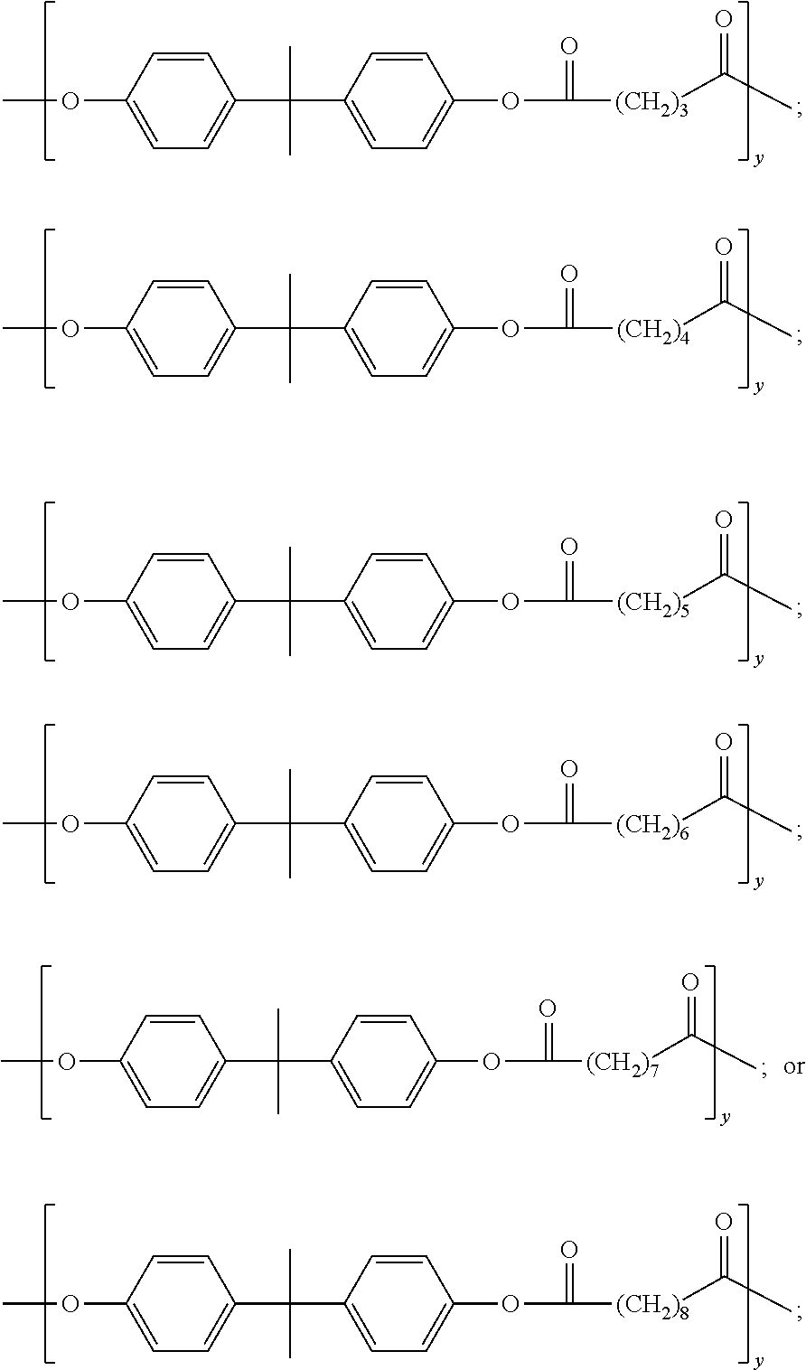
wherein y is 1 to 6.


wherein the Block A and Block B are independently selected from the above lists.

wherein the Block A and Block B are independently selected from the above lists. R1 to R5 and R7 to R10 are defined in the present embodiments discussed above.

wherein i, the degree of polymerization, is a positive integer of between 20 and about 80. While the A-B diblock copolymer is comprising of a bisphenol A polycarbonate segmental block (A) linearly linking to a phthalic acid containing segmental block (B) terminal; the A-B diblock copolymer is a film forming copolymer as represented by the molecular structures described in Formula (IA) and Formula (IB) below:

wherein z represents the number of bisphenol A repeating units in segmental block (A) of from about 9 to about 18, y is number of repeating phthalic acid segmental block (B) of from about 1 to about 2, and n is the degree of polymerization between about 20 and about 90 for the copolymer having a weight average molecular weight between about 100,000 and about 250,000 and mixtures thereof. The disclosed charge transport layer has a thickness of from about 20 to about 40 micrometers.

wherein j, the degree of polymerization, is a positive integer of between about 50 and about 200.


wherein x is an integer between about 40 and about 50 while y and z are integers representing a number of the respective repeating units; a modified bishpenol C polycarbonate derived from the modification of poly(4,4′-isopropylidene diphenyl carbonate) having a small fraction of polydimethyl siloxane in the polymer back bone and has the formula of:

wherein x is an integer between about 40 and about 50 while y and z are integers representing a number of the respective repeating units; and a modification of the modified bisphenol Z polycarbonate of poly(4,4′-diphenyl-1,1′-cyclohexane carbonate), it has a small fraction of a short polydimethyl siloxane segment homogeneously inserted in the polymer back bone, to give the following formula:

wherein x is an integer between about 40 and about 50 while y and z are integers representing a number of the respective repeating units, and mixtures thereof. In all the above formulas of the low surface energy random copolymer, the respective repeating units of y is between about 1 and about 6 and z is between about 9 and about 54. The weight average molecular weight of the low surface energy siloxane/bisphenol type random copolymers of the above formulas is between about 20,000 and about 200,000. Thus, the redesigned low surface energy polymer blended

wherein a, b, p and q are integers representing a number of repeating units;

wherein a, b, c, d, p and q are integers representing a number of repeating units;

wherein a, b and p are integers representing the number of repeating units;

wherein a, b, c, p and q are integers representing the number of repeating units;

wherein the polymer has an polyalkyl and polyaryl siloxane main chain, and wherein a, b and p are integers representing the number of repeating units;

wherein a, p and q are integers representing the number of repeating units; and

wherein a, b and p are integers representing the number of repeating units. The weight average molecular weight of the low surface energy polycarbonates of the above formulas is between about 20,000 and about 200,000.

wherein j, the degree of polymerization, is a positive integer of between about 50 and about 200.
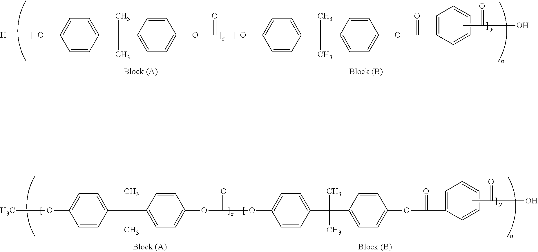
wherein z represents the number of bisphenol A repeating units in block A and is from about 9 to about 18, y represents the number of repeating phthalic acid in block B and is from about 1 to about 2, and n represents the degree of polymerization of di-block copolymer and is from about 20 to about 80, and mixtures thereof

wherein x is an integer between about 40 and about 50, while the respective repeating units of y is between about 1 and 6 and z is between about 9 and about 54.
| TABLE 1 | ||||||||
| Imaging | ||||||||
| Member | CTL BinderType | Vo | S | Vc | Vr | Ve=6.0 | Vdepl | Vdd |
| Control | STD FPC (PCA) | 799 | 350 | 161 | 26.2 | 44.7 | 56.0 | −34.1 |
| Disclosure II | Polymer Blend | 799 | 332 | 166 | 26.5 | 47.6 | 53.6 | −35.0 |
| after 10K cycles |
| Control | STD FPC (PCA) | 799 | 331 | 195 | 45.6 | 74.1 | 104.7 | −54.1 |
| Disclosure II | Polymer Blend | 799 | 324 | 183 | 32.3 | 59.2 | 105.0 | −37.2 |
| TABLE 2 | |||
| Coefficient of | Tape Peel off | ||
| Imaging Member | Surface Energy | Friction (against | Strength |
| (CTL type) | (dynes/cm) | blade) | (grams/cm) |
| Control | 32 | 1.21 | 246 |
| Disclosure II | 21 | 0.65 | 51 |
Claims (20)
R1


R1

R1


Priority Applications (1)
| Application Number | Priority Date | Filing Date | Title |
|---|---|---|---|
| US14/638,361 US9482969B2 (en) | 2013-08-16 | 2015-03-04 | Imaging members having electrically and mechanically tuned imaging layers |
Applications Claiming Priority (2)
| Application Number | Priority Date | Filing Date | Title |
|---|---|---|---|
| US13/969,371 US9046798B2 (en) | 2013-08-16 | 2013-08-16 | Imaging members having electrically and mechanically tuned imaging layers |
| US14/638,361 US9482969B2 (en) | 2013-08-16 | 2015-03-04 | Imaging members having electrically and mechanically tuned imaging layers |
Related Parent Applications (1)
| Application Number | Title | Priority Date | Filing Date |
|---|---|---|---|
| US13/969,371 Division US9046798B2 (en) | 2013-08-16 | 2013-08-16 | Imaging members having electrically and mechanically tuned imaging layers |
Publications (2)
| Publication Number | Publication Date |
|---|---|
| US20150177629A1 US20150177629A1 (en) | 2015-06-25 |
| US9482969B2 true US9482969B2 (en) | 2016-11-01 |
Family
ID=52467077
Family Applications (2)
| Application Number | Title | Priority Date | Filing Date |
|---|---|---|---|
| US13/969,371 Expired - Fee Related US9046798B2 (en) | 2013-08-16 | 2013-08-16 | Imaging members having electrically and mechanically tuned imaging layers |
| US14/638,361 Active US9482969B2 (en) | 2013-08-16 | 2015-03-04 | Imaging members having electrically and mechanically tuned imaging layers |
Family Applications Before (1)
| Application Number | Title | Priority Date | Filing Date |
|---|---|---|---|
| US13/969,371 Expired - Fee Related US9046798B2 (en) | 2013-08-16 | 2013-08-16 | Imaging members having electrically and mechanically tuned imaging layers |
Country Status (1)
| Country | Link |
|---|---|
| US (2) | US9046798B2 (en) |
Citations (41)
| Publication number | Priority date | Publication date | Assignee | Title |
|---|---|---|---|---|
| US3121006A (en) | 1957-06-26 | 1964-02-11 | Xerox Corp | Photo-active member for xerography |
| US3820989A (en) | 1969-09-30 | 1974-06-28 | Eastman Kodak Co | Tri-substituted methanes as organic photoconductors |
| US3837851A (en) | 1973-01-15 | 1974-09-24 | Ibm | Photoconductor overcoated with triarylpyrazoline charge transport layer |
| US3895944A (en) | 1972-08-14 | 1975-07-22 | Hoechst Ag | Electrophotographic recording material having a layered structure of charge generating and charge transport layers |
| US4150987A (en) | 1977-10-17 | 1979-04-24 | International Business Machines Corporation | Hydrazone containing charge transport element and photoconductive process of using same |
| US4245021A (en) | 1978-02-17 | 1981-01-13 | Ricoh Co., Ltd. | Electrophotographic element having charge transport layer |
| US4256821A (en) | 1978-12-21 | 1981-03-17 | Ricoh Company, Ltd. | Electrophotographic element with carbazole-phenyhydrazone charge transport layer |
| US4265990A (en) | 1977-05-04 | 1981-05-05 | Xerox Corporation | Imaging system with a diamine charge transport material in a polycarbonate resin |
| US4278746A (en) | 1978-06-21 | 1981-07-14 | Konishiroku Photo Industry Co., Ltd. | Photosensitive elements for electrophotography |
| US4286033A (en) | 1980-03-05 | 1981-08-25 | Xerox Corporation | Trapping layer overcoated inorganic photoresponsive device |
| US4291110A (en) | 1979-06-11 | 1981-09-22 | Xerox Corporation | Siloxane hole trapping layer for overcoated photoreceptors |
| US4297426A (en) | 1979-05-28 | 1981-10-27 | Ricoh Co., Ltd. | Electrophotographic element with carbazole hydrazone or anile charge transport compounds |
| US4315982A (en) | 1979-08-23 | 1982-02-16 | Copyer Co., Ltd. | Styryl pyrazoline compounds, process for production thereof, and electrophoto graphic material comprising said compounds |
| US4338388A (en) | 1978-10-13 | 1982-07-06 | Ricoh Company, Limited | Electrophotographic element with a phenyhydrazone charge transport layer |
| US4338387A (en) | 1981-03-02 | 1982-07-06 | Xerox Corporation | Overcoated photoreceptor containing inorganic electron trapping and hole trapping layers |
| US4385106A (en) | 1980-02-28 | 1983-05-24 | Ricoh Co., Ltd. | Charge transfer layer with styryl hydrazones |
| US4387147A (en) | 1979-12-08 | 1983-06-07 | Ricoh Co., Ltd. | Electrophotographic element containing hydrazone compounds in charge transport layers |
| US4399208A (en) | 1980-11-22 | 1983-08-16 | Canon Kabushiki Kaisha | Electrophotographic photosensitive member |
| US4399207A (en) | 1981-07-31 | 1983-08-16 | Canon Kabushiki Kaisha | Electrophotographic photosensitive member with hydrazone compound |
| US4587189A (en) | 1985-05-24 | 1986-05-06 | Xerox Corporation | Photoconductive imaging members with perylene pigment compositions |
| US4664995A (en) | 1985-10-24 | 1987-05-12 | Xerox Corporation | Electrostatographic imaging members |
| US4988597A (en) | 1989-12-29 | 1991-01-29 | Xerox Corporation | Conductive and blocking layers for electrophotographic imaging members |
| US5215839A (en) | 1991-12-23 | 1993-06-01 | Xerox Corporation | Method and system for reducing surface reflections from an electrophotographic imaging member |
| US5244762A (en) | 1992-01-03 | 1993-09-14 | Xerox Corporation | Electrophotographic imaging member with blocking layer containing uncrosslinked chemically modified copolymer |
| US5660961A (en) | 1996-01-11 | 1997-08-26 | Xerox Corporation | Electrophotographic imaging member having enhanced layer adhesion and freedom from reflection interference |
| US5697024A (en) | 1996-01-11 | 1997-12-09 | Xerox Corporation | Differential increase in dark decay comparison |
| US5703487A (en) | 1996-01-11 | 1997-12-30 | Xerox Corporation | Detection of charge deficient spot susceptibility |
| US5756245A (en) | 1997-06-05 | 1998-05-26 | Xerox Corporation | Photoconductive imaging members |
| US5958638A (en) | 1997-06-23 | 1999-09-28 | Sharp Kabushiki Kaisha | Electrophotographic photoconductor and method of producing same |
| US6008653A (en) | 1997-10-30 | 1999-12-28 | Xerox Corporation | Contactless system for detecting microdefects on electrostatographic members |
| US6119536A (en) | 1997-10-30 | 2000-09-19 | Xerox Corporation | Constant distance contactless device |
| US6124514A (en) | 1996-02-03 | 2000-09-26 | Krupp Uhde Gmbh | Process for generating pure benzene from reformed gasoline |
| US6150824A (en) | 1997-10-30 | 2000-11-21 | Xerox Corporation | Contactless system for detecting subtle surface potential charge patterns |
| US6214514B1 (en) | 1999-09-29 | 2001-04-10 | Xerox Corporation | Process for fabricating electrophotographic imaging member |
| US6326111B1 (en) | 2000-11-15 | 2001-12-04 | Xerox Corporation | Stable charge transport layer dispersion containing polytetrafluoroethylene particles and hydrophobic silica |
| US6756169B2 (en) | 2002-07-23 | 2004-06-29 | Xerox Corporation | Imaging members |
| US6933089B2 (en) | 2002-12-16 | 2005-08-23 | Xerox Corporation | Imaging member |
| US7018756B2 (en) | 2003-09-05 | 2006-03-28 | Xerox Corporation | Dual charge transport layer and photoconductive imaging member including the same |
| US7033714B2 (en) | 2002-12-16 | 2006-04-25 | Xerox Corporation | Imaging members |
| US7413835B2 (en) | 2005-07-14 | 2008-08-19 | Xerox Corporation | Imaging members |
| US7592111B2 (en) | 2004-11-05 | 2009-09-22 | Xerox Corporation | Imaging member |
Family Cites Families (3)
| Publication number | Priority date | Publication date | Assignee | Title |
|---|---|---|---|---|
| US8007970B2 (en) * | 2008-04-07 | 2011-08-30 | Xerox Corporation | Low friction electrostatographic imaging member |
| US8232030B2 (en) * | 2010-03-17 | 2012-07-31 | Xerox Corporation | Curl-free imaging members with a slippery surface |
| US8470505B2 (en) * | 2010-06-10 | 2013-06-25 | Xerox Corporation | Imaging members having improved imaging layers |
-
2013
- 2013-08-16 US US13/969,371 patent/US9046798B2/en not_active Expired - Fee Related
-
2015
- 2015-03-04 US US14/638,361 patent/US9482969B2/en active Active
Patent Citations (41)
| Publication number | Priority date | Publication date | Assignee | Title |
|---|---|---|---|---|
| US3121006A (en) | 1957-06-26 | 1964-02-11 | Xerox Corp | Photo-active member for xerography |
| US3820989A (en) | 1969-09-30 | 1974-06-28 | Eastman Kodak Co | Tri-substituted methanes as organic photoconductors |
| US3895944A (en) | 1972-08-14 | 1975-07-22 | Hoechst Ag | Electrophotographic recording material having a layered structure of charge generating and charge transport layers |
| US3837851A (en) | 1973-01-15 | 1974-09-24 | Ibm | Photoconductor overcoated with triarylpyrazoline charge transport layer |
| US4265990A (en) | 1977-05-04 | 1981-05-05 | Xerox Corporation | Imaging system with a diamine charge transport material in a polycarbonate resin |
| US4150987A (en) | 1977-10-17 | 1979-04-24 | International Business Machines Corporation | Hydrazone containing charge transport element and photoconductive process of using same |
| US4245021A (en) | 1978-02-17 | 1981-01-13 | Ricoh Co., Ltd. | Electrophotographic element having charge transport layer |
| US4278746A (en) | 1978-06-21 | 1981-07-14 | Konishiroku Photo Industry Co., Ltd. | Photosensitive elements for electrophotography |
| US4338388A (en) | 1978-10-13 | 1982-07-06 | Ricoh Company, Limited | Electrophotographic element with a phenyhydrazone charge transport layer |
| US4256821A (en) | 1978-12-21 | 1981-03-17 | Ricoh Company, Ltd. | Electrophotographic element with carbazole-phenyhydrazone charge transport layer |
| US4297426A (en) | 1979-05-28 | 1981-10-27 | Ricoh Co., Ltd. | Electrophotographic element with carbazole hydrazone or anile charge transport compounds |
| US4291110A (en) | 1979-06-11 | 1981-09-22 | Xerox Corporation | Siloxane hole trapping layer for overcoated photoreceptors |
| US4315982A (en) | 1979-08-23 | 1982-02-16 | Copyer Co., Ltd. | Styryl pyrazoline compounds, process for production thereof, and electrophoto graphic material comprising said compounds |
| US4387147A (en) | 1979-12-08 | 1983-06-07 | Ricoh Co., Ltd. | Electrophotographic element containing hydrazone compounds in charge transport layers |
| US4385106A (en) | 1980-02-28 | 1983-05-24 | Ricoh Co., Ltd. | Charge transfer layer with styryl hydrazones |
| US4286033A (en) | 1980-03-05 | 1981-08-25 | Xerox Corporation | Trapping layer overcoated inorganic photoresponsive device |
| US4399208A (en) | 1980-11-22 | 1983-08-16 | Canon Kabushiki Kaisha | Electrophotographic photosensitive member |
| US4338387A (en) | 1981-03-02 | 1982-07-06 | Xerox Corporation | Overcoated photoreceptor containing inorganic electron trapping and hole trapping layers |
| US4399207A (en) | 1981-07-31 | 1983-08-16 | Canon Kabushiki Kaisha | Electrophotographic photosensitive member with hydrazone compound |
| US4587189A (en) | 1985-05-24 | 1986-05-06 | Xerox Corporation | Photoconductive imaging members with perylene pigment compositions |
| US4664995A (en) | 1985-10-24 | 1987-05-12 | Xerox Corporation | Electrostatographic imaging members |
| US4988597A (en) | 1989-12-29 | 1991-01-29 | Xerox Corporation | Conductive and blocking layers for electrophotographic imaging members |
| US5215839A (en) | 1991-12-23 | 1993-06-01 | Xerox Corporation | Method and system for reducing surface reflections from an electrophotographic imaging member |
| US5244762A (en) | 1992-01-03 | 1993-09-14 | Xerox Corporation | Electrophotographic imaging member with blocking layer containing uncrosslinked chemically modified copolymer |
| US5660961A (en) | 1996-01-11 | 1997-08-26 | Xerox Corporation | Electrophotographic imaging member having enhanced layer adhesion and freedom from reflection interference |
| US5697024A (en) | 1996-01-11 | 1997-12-09 | Xerox Corporation | Differential increase in dark decay comparison |
| US5703487A (en) | 1996-01-11 | 1997-12-30 | Xerox Corporation | Detection of charge deficient spot susceptibility |
| US6124514A (en) | 1996-02-03 | 2000-09-26 | Krupp Uhde Gmbh | Process for generating pure benzene from reformed gasoline |
| US5756245A (en) | 1997-06-05 | 1998-05-26 | Xerox Corporation | Photoconductive imaging members |
| US5958638A (en) | 1997-06-23 | 1999-09-28 | Sharp Kabushiki Kaisha | Electrophotographic photoconductor and method of producing same |
| US6008653A (en) | 1997-10-30 | 1999-12-28 | Xerox Corporation | Contactless system for detecting microdefects on electrostatographic members |
| US6119536A (en) | 1997-10-30 | 2000-09-19 | Xerox Corporation | Constant distance contactless device |
| US6150824A (en) | 1997-10-30 | 2000-11-21 | Xerox Corporation | Contactless system for detecting subtle surface potential charge patterns |
| US6214514B1 (en) | 1999-09-29 | 2001-04-10 | Xerox Corporation | Process for fabricating electrophotographic imaging member |
| US6326111B1 (en) | 2000-11-15 | 2001-12-04 | Xerox Corporation | Stable charge transport layer dispersion containing polytetrafluoroethylene particles and hydrophobic silica |
| US6756169B2 (en) | 2002-07-23 | 2004-06-29 | Xerox Corporation | Imaging members |
| US6933089B2 (en) | 2002-12-16 | 2005-08-23 | Xerox Corporation | Imaging member |
| US7033714B2 (en) | 2002-12-16 | 2006-04-25 | Xerox Corporation | Imaging members |
| US7018756B2 (en) | 2003-09-05 | 2006-03-28 | Xerox Corporation | Dual charge transport layer and photoconductive imaging member including the same |
| US7592111B2 (en) | 2004-11-05 | 2009-09-22 | Xerox Corporation | Imaging member |
| US7413835B2 (en) | 2005-07-14 | 2008-08-19 | Xerox Corporation | Imaging members |
Also Published As
| Publication number | Publication date |
|---|---|
| US9046798B2 (en) | 2015-06-02 |
| US20150050588A1 (en) | 2015-02-19 |
| US20150177629A1 (en) | 2015-06-25 |
Similar Documents
| Publication | Publication Date | Title |
|---|---|---|
| US7455941B2 (en) | Imaging member with multilayer anti-curl back coating | |
| US7462434B2 (en) | Imaging member with low surface energy polymer in anti-curl back coating layer | |
| US8168356B2 (en) | Structurally simplified flexible imaging members | |
| US7422831B2 (en) | Anticurl back coating layer electrophotographic imaging members | |
| US8470505B2 (en) | Imaging members having improved imaging layers | |
| US8232030B2 (en) | Curl-free imaging members with a slippery surface | |
| US20100297544A1 (en) | Flexible imaging members having a plasticized imaging layer | |
| US20090253056A1 (en) | Low friction electrostatographic imaging member | |
| US8263301B2 (en) | Low friction electrostatographic imaging member | |
| US8124305B2 (en) | Flexible imaging members without anticurl layer | |
| US8263298B1 (en) | Electrically tunable and stable imaging members | |
| US8465892B2 (en) | Chemically resistive and lubricated overcoat | |
| US8003285B2 (en) | Flexible imaging member belts | |
| US8241825B2 (en) | Flexible imaging member belts | |
| US8475983B2 (en) | Imaging members having a chemical resistive overcoat layer | |
| US8173341B2 (en) | Flexible imaging members without anticurl layer | |
| US8007970B2 (en) | Low friction electrostatographic imaging member | |
| US9091949B2 (en) | Imaging members having electrically and mechanically tuned imaging layers | |
| US8232032B2 (en) | Low friction electrostatographic imaging member | |
| US8404413B2 (en) | Flexible imaging members having stress-free imaging layer(s) | |
| US9017908B2 (en) | Photoelectrical stable imaging members | |
| US9482969B2 (en) | Imaging members having electrically and mechanically tuned imaging layers | |
| US9075327B2 (en) | Imaging members and methods for making the same | |
| US9017907B2 (en) | Flexible imaging members having externally plasticized imaging layer(s) | |
| US20090253063A1 (en) | Low friction electrostatographic imaging member |
Legal Events
| Date | Code | Title | Description |
|---|---|---|---|
| STCF | Information on status: patent grant |
Free format text: PATENTED CASE |
|
| FEPP | Fee payment procedure |
Free format text: MAINTENANCE FEE REMINDER MAILED (ORIGINAL EVENT CODE: REM.); ENTITY STATUS OF PATENT OWNER: LARGE ENTITY |
|
| FEPP | Fee payment procedure |
Free format text: SURCHARGE FOR LATE PAYMENT, LARGE ENTITY (ORIGINAL EVENT CODE: M1554); ENTITY STATUS OF PATENT OWNER: LARGE ENTITY |
|
| MAFP | Maintenance fee payment |
Free format text: PAYMENT OF MAINTENANCE FEE, 4TH YEAR, LARGE ENTITY (ORIGINAL EVENT CODE: M1551); ENTITY STATUS OF PATENT OWNER: LARGE ENTITY Year of fee payment: 4 |
|
| AS | Assignment |
Owner name: CITIBANK, N.A., AS AGENT, DELAWARE Free format text: SECURITY INTEREST;ASSIGNOR:XEROX CORPORATION;REEL/FRAME:062740/0214 Effective date: 20221107 |
|
| AS | Assignment |
Owner name: XEROX CORPORATION, CONNECTICUT Free format text: RELEASE OF SECURITY INTEREST IN PATENTS AT R/F 062740/0214;ASSIGNOR:CITIBANK, N.A., AS AGENT;REEL/FRAME:063694/0122 Effective date: 20230517 |
|
| AS | Assignment |
Owner name: CITIBANK, N.A., AS COLLATERAL AGENT, NEW YORK Free format text: SECURITY INTEREST;ASSIGNOR:XEROX CORPORATION;REEL/FRAME:064760/0389 Effective date: 20230621 |
|
| AS | Assignment |
Owner name: JEFFERIES FINANCE LLC, AS COLLATERAL AGENT, NEW YORK Free format text: SECURITY INTEREST;ASSIGNOR:XEROX CORPORATION;REEL/FRAME:065628/0019 Effective date: 20231117 |
|
| AS | Assignment |
Owner name: CITIBANK, N.A., AS COLLATERAL AGENT, NEW YORK Free format text: SECURITY INTEREST;ASSIGNOR:XEROX CORPORATION;REEL/FRAME:066741/0001 Effective date: 20240206 |